KR20200032527A - Operating method of memory system and memory system - Google Patents
Operating method of memory system and memory system Download PDFInfo
- Publication number
- KR20200032527A KR20200032527A KR1020180111661A KR20180111661A KR20200032527A KR 20200032527 A KR20200032527 A KR 20200032527A KR 1020180111661 A KR1020180111661 A KR 1020180111661A KR 20180111661 A KR20180111661 A KR 20180111661A KR 20200032527 A KR20200032527 A KR 20200032527A
- Authority
- KR
- South Korea
- Prior art keywords
- logical address
- block
- valid data
- blocks
- memory
- Prior art date
Links
Images


Classifications
-
- G—PHYSICS
- G06—COMPUTING; CALCULATING OR COUNTING
- G06F—ELECTRIC DIGITAL DATA PROCESSING
- G06F3/00—Input arrangements for transferring data to be processed into a form capable of being handled by the computer; Output arrangements for transferring data from processing unit to output unit, e.g. interface arrangements
- G06F3/06—Digital input from, or digital output to, record carriers, e.g. RAID, emulated record carriers or networked record carriers
- G06F3/0601—Interfaces specially adapted for storage systems
- G06F3/0602—Interfaces specially adapted for storage systems specifically adapted to achieve a particular effect
- G06F3/0614—Improving the reliability of storage systems
- G06F3/0619—Improving the reliability of storage systems in relation to data integrity, e.g. data losses, bit errors
-
- G—PHYSICS
- G06—COMPUTING; CALCULATING OR COUNTING
- G06F—ELECTRIC DIGITAL DATA PROCESSING
- G06F12/00—Accessing, addressing or allocating within memory systems or architectures
- G06F12/02—Addressing or allocation; Relocation
- G06F12/0223—User address space allocation, e.g. contiguous or non contiguous base addressing
- G06F12/023—Free address space management
- G06F12/0238—Memory management in non-volatile memory, e.g. resistive RAM or ferroelectric memory
- G06F12/0246—Memory management in non-volatile memory, e.g. resistive RAM or ferroelectric memory in block erasable memory, e.g. flash memory
-
- G—PHYSICS
- G06—COMPUTING; CALCULATING OR COUNTING
- G06F—ELECTRIC DIGITAL DATA PROCESSING
- G06F11/00—Error detection; Error correction; Monitoring
- G06F11/07—Responding to the occurrence of a fault, e.g. fault tolerance
- G06F11/14—Error detection or correction of the data by redundancy in operation
- G06F11/1402—Saving, restoring, recovering or retrying
- G06F11/1446—Point-in-time backing up or restoration of persistent data
- G06F11/1448—Management of the data involved in backup or backup restore
-
- G—PHYSICS
- G06—COMPUTING; CALCULATING OR COUNTING
- G06F—ELECTRIC DIGITAL DATA PROCESSING
- G06F11/00—Error detection; Error correction; Monitoring
- G06F11/07—Responding to the occurrence of a fault, e.g. fault tolerance
- G06F11/14—Error detection or correction of the data by redundancy in operation
- G06F11/1402—Saving, restoring, recovering or retrying
- G06F11/1446—Point-in-time backing up or restoration of persistent data
- G06F11/1458—Management of the backup or restore process
- G06F11/1464—Management of the backup or restore process for networked environments
-
- G—PHYSICS
- G06—COMPUTING; CALCULATING OR COUNTING
- G06F—ELECTRIC DIGITAL DATA PROCESSING
- G06F12/00—Accessing, addressing or allocating within memory systems or architectures
- G06F12/02—Addressing or allocation; Relocation
- G06F12/0223—User address space allocation, e.g. contiguous or non contiguous base addressing
- G06F12/0292—User address space allocation, e.g. contiguous or non contiguous base addressing using tables or multilevel address translation means
-
- G—PHYSICS
- G06—COMPUTING; CALCULATING OR COUNTING
- G06F—ELECTRIC DIGITAL DATA PROCESSING
- G06F3/00—Input arrangements for transferring data to be processed into a form capable of being handled by the computer; Output arrangements for transferring data from processing unit to output unit, e.g. interface arrangements
- G06F3/06—Digital input from, or digital output to, record carriers, e.g. RAID, emulated record carriers or networked record carriers
- G06F3/0601—Interfaces specially adapted for storage systems
- G06F3/0602—Interfaces specially adapted for storage systems specifically adapted to achieve a particular effect
- G06F3/061—Improving I/O performance
-
- G—PHYSICS
- G06—COMPUTING; CALCULATING OR COUNTING
- G06F—ELECTRIC DIGITAL DATA PROCESSING
- G06F3/00—Input arrangements for transferring data to be processed into a form capable of being handled by the computer; Output arrangements for transferring data from processing unit to output unit, e.g. interface arrangements
- G06F3/06—Digital input from, or digital output to, record carriers, e.g. RAID, emulated record carriers or networked record carriers
- G06F3/0601—Interfaces specially adapted for storage systems
- G06F3/0628—Interfaces specially adapted for storage systems making use of a particular technique
- G06F3/0638—Organizing or formatting or addressing of data
- G06F3/064—Management of blocks
-
- G—PHYSICS
- G06—COMPUTING; CALCULATING OR COUNTING
- G06F—ELECTRIC DIGITAL DATA PROCESSING
- G06F3/00—Input arrangements for transferring data to be processed into a form capable of being handled by the computer; Output arrangements for transferring data from processing unit to output unit, e.g. interface arrangements
- G06F3/06—Digital input from, or digital output to, record carriers, e.g. RAID, emulated record carriers or networked record carriers
- G06F3/0601—Interfaces specially adapted for storage systems
- G06F3/0628—Interfaces specially adapted for storage systems making use of a particular technique
- G06F3/0646—Horizontal data movement in storage systems, i.e. moving data in between storage devices or systems
- G06F3/0647—Migration mechanisms
-
- G—PHYSICS
- G06—COMPUTING; CALCULATING OR COUNTING
- G06F—ELECTRIC DIGITAL DATA PROCESSING
- G06F3/00—Input arrangements for transferring data to be processed into a form capable of being handled by the computer; Output arrangements for transferring data from processing unit to output unit, e.g. interface arrangements
- G06F3/06—Digital input from, or digital output to, record carriers, e.g. RAID, emulated record carriers or networked record carriers
- G06F3/0601—Interfaces specially adapted for storage systems
- G06F3/0668—Interfaces specially adapted for storage systems adopting a particular infrastructure
- G06F3/0671—In-line storage system
- G06F3/0673—Single storage device
- G06F3/0679—Non-volatile semiconductor memory device, e.g. flash memory, one time programmable memory [OTP]
-
- G—PHYSICS
- G06—COMPUTING; CALCULATING OR COUNTING
- G06F—ELECTRIC DIGITAL DATA PROCESSING
- G06F2212/00—Indexing scheme relating to accessing, addressing or allocation within memory systems or architectures
- G06F2212/10—Providing a specific technical effect
- G06F2212/1008—Correctness of operation, e.g. memory ordering
-
- G—PHYSICS
- G06—COMPUTING; CALCULATING OR COUNTING
- G06F—ELECTRIC DIGITAL DATA PROCESSING
- G06F2212/00—Indexing scheme relating to accessing, addressing or allocation within memory systems or architectures
- G06F2212/10—Providing a specific technical effect
- G06F2212/1016—Performance improvement
-
- G—PHYSICS
- G06—COMPUTING; CALCULATING OR COUNTING
- G06F—ELECTRIC DIGITAL DATA PROCESSING
- G06F2212/00—Indexing scheme relating to accessing, addressing or allocation within memory systems or architectures
- G06F2212/20—Employing a main memory using a specific memory technology
- G06F2212/202—Non-volatile memory
- G06F2212/2022—Flash memory
-
- G—PHYSICS
- G06—COMPUTING; CALCULATING OR COUNTING
- G06F—ELECTRIC DIGITAL DATA PROCESSING
- G06F2212/00—Indexing scheme relating to accessing, addressing or allocation within memory systems or architectures
- G06F2212/72—Details relating to flash memory management
- G06F2212/7201—Logical to physical mapping or translation of blocks or pages
-
- G—PHYSICS
- G06—COMPUTING; CALCULATING OR COUNTING
- G06F—ELECTRIC DIGITAL DATA PROCESSING
- G06F2212/00—Indexing scheme relating to accessing, addressing or allocation within memory systems or architectures
- G06F2212/72—Details relating to flash memory management
- G06F2212/7205—Cleaning, compaction, garbage collection, erase control
-
- Y—GENERAL TAGGING OF NEW TECHNOLOGICAL DEVELOPMENTS; GENERAL TAGGING OF CROSS-SECTIONAL TECHNOLOGIES SPANNING OVER SEVERAL SECTIONS OF THE IPC; TECHNICAL SUBJECTS COVERED BY FORMER USPC CROSS-REFERENCE ART COLLECTIONS [XRACs] AND DIGESTS
- Y02—TECHNOLOGIES OR APPLICATIONS FOR MITIGATION OR ADAPTATION AGAINST CLIMATE CHANGE
- Y02D—CLIMATE CHANGE MITIGATION TECHNOLOGIES IN INFORMATION AND COMMUNICATION TECHNOLOGIES [ICT], I.E. INFORMATION AND COMMUNICATION TECHNOLOGIES AIMING AT THE REDUCTION OF THEIR OWN ENERGY USE
- Y02D10/00—Energy efficient computing, e.g. low power processors, power management or thermal management
Abstract
Description
본 발명은 메모리 시스템에 관한 것으로, 더욱 상세하게는 비휘발성 메모리 장치를 포함하는 메모리 시스템에 관한 것이다.The present invention relates to a memory system, and more particularly, to a memory system including a nonvolatile memory device.
메모리 시스템은 외부 장치의 라이트 요청에 응답하여, 외부 장치로부터 제공된 데이터를 저장하도록 구성될 수 있다. 또한, 메모리 시스템은 외부 장치의 리드 요청에 응답하여, 저장된 데이터를 외부 장치로 제공하도록 구성될 수 있다. 외부 장치는 데이터를 처리할 수 있는 전자 장치로서, 컴퓨터, 디지털 카메라 또는 휴대폰 등을 포함할 수 있다. 메모리 시스템은 외부 장치에 내장되어 동작하거나, 분리 가능한 형태로 제작되어 외부 장치에 연결됨으로써 동작할 수 있다.The memory system may be configured to store data provided from the external device in response to a write request from the external device. Further, the memory system may be configured to provide stored data to the external device in response to a read request from the external device. The external device is an electronic device capable of processing data, and may include a computer, a digital camera, or a mobile phone. The memory system may operate by being built in an external device or manufactured in a detachable form and connected to an external device.
메모리 장치를 이용한 메모리 시스템은 기계적인 구동부가 없어서 안정성 및 내구성이 뛰어나며 정보의 액세스 속도가 매우 빠르고 전력 소모가 적다는 장점이 있다. 이러한 장점을 갖는 메모리 시스템은 USB(Universal Serial Bus) 메모리 장치, 다양한 인터페이스를 갖는 메모리 카드, UFS(Universal Flash Storage) 장치, 솔리드 스테이트 드라이브(Solid State Drive, 이하, SSD라 칭함)를 포함한다.A memory system using a memory device has the advantages of excellent stability and durability, as there is no mechanical driving unit, and an information access speed is very fast and power consumption is low. A memory system having such an advantage includes a universal serial bus (USB) memory device, a memory card having various interfaces, a universal flash storage (UFS) device, and a solid state drive (hereinafter referred to as SSD).
본 발명의 실시 예는, 비휘발성 메모리 장치의 내부 백업 동작의 효율을 높일 수 있는 메모리 시스템을 제공하는 데 있다.An embodiment of the present invention is to provide a memory system capable of increasing the efficiency of an internal backup operation of a nonvolatile memory device.
본 발명의 실시 예에 따라 각각이 기설정된 논리 어드레스 범위를 갖는 복수의 논리 어드레스 그룹들이 적용되는 메모리 시스템의 동작 방법은, 희생(victim) 블록을 선택하는 단계; 빈 블록들 중에서 복수의 타겟 블록들을 선택하는 단계; 상기 타겟 블록들 각각에 상기 논리 어드레스 그룹들 중 적어도 하나의 논리 어드레스 그룹을 맵핑하는 단계; 상기 논리 어드레스 그룹들 중에서, 상기 희생 블록에 저장된 제1 유효 데이터의 논리 어드레스를 포함하는 제1 논리 어드레스 그룹을 판단하는 단계; 상기 제1 유효 데이터를 상기 타겟 블록들 중에서 상기 제1 논리 어드레스 그룹에 맵핑된 제1 타겟 블록에 백업하는 단계를 포함할 수 있다.According to an embodiment of the present invention, a method of operating a memory system to which a plurality of logical address groups, each having a predetermined logical address range, is applied, includes: selecting a victim block; Selecting a plurality of target blocks from among the empty blocks; Mapping at least one logical address group of the logical address groups to each of the target blocks; Determining, among the logical address groups, a first logical address group including a logical address of first valid data stored in the victim block; And backing up the first valid data to a first target block mapped to the first logical address group among the target blocks.
본 발명의 실시 예에 따라 각각이 기설정된 논리 어드레스 범위를 갖는 복수의 논리 어드레스 그룹들이 적용되는 메모리 시스템의 동작 방법은, 희생 블록을 선택하는 단계; 빈 블록들 중에서 상기 희생 블록에 저장된 유효 데이터가 백업되는 타겟 블록을 선택하는 단계; 상기 논리 어드레스 그룹들의 백업 순서를 결정하되, 상기 백업 순서는 상기 각각의 논리 어드레스 그룹들에 대응하는 유효 데이터가 상기 타겟 블록에 백업되는 순서인, 결정하는 단계; 및 상기 백업 순서에 기초하여 상기 유효 데이터 중 선택된 유효 데이터를 상기 타겟 블록으로 백업하는 단계를 포함할 수 있다.According to an embodiment of the present invention, a method of operating a memory system to which a plurality of logical address groups, each having a predetermined logical address range, is applied includes: selecting a victim block; Selecting a target block from which valid data stored in the victim block is backed up among empty blocks; Determining a backup order of the logical address groups, wherein the backup order is an order in which valid data corresponding to the respective logical address groups are backed up to the target block; And backing up the valid data selected from the valid data to the target block based on the backup order.
본 발명의 실시 예에 따라 각각이 기설정된 논리 어드레스 범위를 갖는 복수의 논리 어드레스 그룹들이 적용되는 메모리 시스템은, 복수의 메모리 블록들을 포함하는 비휘발성 메모리 장치들; 및 상기 메모리 블록들을 상기 비휘발성 메모리 장치들에 걸쳐 복수의 슈퍼 블록들로 그룹핑하고, 상기 슈퍼 블록들 중에서 희생(victim) 블록을 선택하고, 상기 희생 블록에 대한 내부 백업 동작을 제어하도록 구성된 컨트롤러를 포함하되, 상기 컨트롤러는, 상기 논리 어드레스 그룹들 중 상기 희생 블록에 저장된 유효 데이터의 논리 어드레스들을 포함하는 논리 어드레스 그룹들을 판단하고, 상기 판단된 논리 어드레스 그룹들에 맵핑된 위치들에 상기 유효 데이터를 백업할 수 있다.A memory system to which a plurality of logical address groups, each having a preset logical address range, according to an embodiment of the present invention is applied, includes: nonvolatile memory devices including a plurality of memory blocks; And a controller configured to group the memory blocks into a plurality of super blocks across the non-volatile memory devices, select a victim block from among the super blocks, and control an internal backup operation for the victim block. The controller may include logical address groups including logical addresses of valid data stored in the victim block among the logical address groups, and transmit the valid data to locations mapped to the determined logical address groups. You can back it up.
본 발명의 실시 예에 따른 메모리 시스템은 기설정된 논리 어드레스 범위에 대응하는 데이터를 동일한 타겟 블록에 저장함으로써, 비휘발성 메모리 장치의 내부 백업 동작의 효율을 높일 수 있다.The memory system according to an embodiment of the present invention can increase the efficiency of an internal backup operation of a nonvolatile memory device by storing data corresponding to a predetermined logical address range in the same target block.
도 1은 본 발명의 실시 예에 따른 메모리 시스템의 구성을 예시적으로 설명하기 위한 블록도이다.
도 2는 도 1의 랜덤 액세스 메모리에서 구동되는 소프트웨어를 예시적으로 설명하기 위한 도면이다.
도 3a는 각각의 논리 어드레스 그룹들에 포함되는 논리 어드레스 범위를 예시적으로 설명하기 위한 도면이다.
도 3b는 맵핑 테이블에 저장되는 정보를 예시적으로 설명하기 위한 도면이다.
도 4는 도 2의 가비지 컬렉션 모듈에 의해서 수행되는 가비지 컬렉션 동작을 설명하기 위한 도면이다.
도 5는 복수의 논리 어드레스 그룹들에 대응하는 유효 데이터가 저장된 희생 블록을 예시적으로 보여주는 도면이다.
도 6은 본 발명의 실시 예에 따라, 도 5의 희생 블록에 저장된 유효 데이터가 2개의 타겟 블록들에 백업되는 경우를 설명하기 위한 도면이다.
도 7은 도 6의 실시 예를 시계열적으로 설명하기 위한 순서도이다.
도 8은 본 발명의 실시 예에 따라, 도 5의 희생 블록에 저장된 유효 데이터가 1개의 타겟 블록에 백업되는 경우를 설명하기 위한 도면이다.
도 9는 도 8의 실시 예를 시계열적으로 설명하기 위한 순서도이다.
도 10은 본 발명의 실시 예에 따른 컨트롤러의 구성을 설명하기 위한 블록도이다.
도 11은 본 발명의 실시 예에 따른 SSD를 포함하는 데이터 처리 시스템을 예시적으로 보여주는 도면이다.
도 12는 본 발명의 실시 예에 따른 메모리 시스템을 포함하는 데이터 처리 시스템을 예시적으로 보여주는 도면이다.
도 13은 본 발명의 실시 예에 따른 메모리 시스템을 포함하는 데이터 처리 시스템을 예시적으로 보여주는 도면이다.
도 14는 본 발명의 실시 예에 따른 메모리 시스템을 포함하는 네트워크 시스템을 예시적으로 보여주는 도면이다.
도 15는 본 발명의 실시 예에 따른 메모리 시스템에 포함된 비휘발성 메모리 장치를 예시적으로 보여주는 블록도이다.1 is a block diagram illustrating an exemplary configuration of a memory system according to an embodiment of the present invention.
FIG. 2 is a diagram for exemplarily explaining software driven in the random access memory of FIG. 1.
3A is a diagram for illustratively explaining a logical address range included in each logical address group.
3B is a diagram for illustratively describing information stored in a mapping table.
FIG. 4 is a diagram illustrating a garbage collection operation performed by the garbage collection module of FIG. 2.
5 is a diagram exemplarily showing a victim block in which valid data corresponding to a plurality of logical address groups is stored.
6 is a diagram for explaining a case in which valid data stored in the sacrificial block of FIG. 5 is backed up to two target blocks according to an embodiment of the present invention.
7 is a flowchart illustrating the embodiment of FIG. 6 in time series.
8 is a diagram for explaining a case in which valid data stored in the sacrificial block of FIG. 5 is backed up to one target block according to an embodiment of the present invention.
9 is a flowchart illustrating the embodiment of FIG. 8 in time series.
10 is a block diagram illustrating the configuration of a controller according to an embodiment of the present invention.
11 is a diagram exemplarily showing a data processing system including an SSD according to an embodiment of the present invention.
12 is a diagram exemplarily showing a data processing system including a memory system according to an embodiment of the present invention.
13 is a diagram exemplarily showing a data processing system including a memory system according to an embodiment of the present invention.
14 is a diagram exemplarily showing a network system including a memory system according to an embodiment of the present invention.
15 is a block diagram exemplarily showing a nonvolatile memory device included in a memory system according to an embodiment of the present invention.
본 발명의 이점 및 특징, 그리고 그것을 달성하는 방법은 첨부되는 도면과 함께 상세하게 후술되어 있는 실시 예들을 통해 설명될 것이다. 그러나 본 발명은 여기에서 설명되는 실시 예들에 한정되지 않고 다른 형태로 구체화될 수도 있다. 단지, 본 실시 예들은 본 발명이 속하는 기술분야에서 통상의 지식을 가진 자에게 본 발명의 기술적 사상을 용이하게 실시할 수 있을 정도로 상세히 설명하기 위하여 제공되는 것이다.Advantages and features of the present invention and a method of achieving the same will be described through embodiments described below in detail with reference to the accompanying drawings. However, the present invention is not limited to the embodiments described herein and may be embodied in other forms. However, the present embodiments are provided to explain in detail that the technical spirit of the present invention can be easily carried out to a person having ordinary knowledge in the technical field to which the present invention pertains.
도면들에 있어서, 본 발명의 실시 예들은 도시된 특정 형태로 제한되는 것이 아니며 명확성을 기하기 위하여 과장된 것이다. 본 명세서에서 특정한 용어들이 사용되었으나. 이는 본 발명을 설명하기 위한 목적에서 사용된 것이며, 의미 한정이나 특허 청구 범위에 기재된 본 발명의 권리 범위를 제한하기 위하여 사용된 것은 아니다.In the drawings, embodiments of the present invention are not limited to the specific form shown and are exaggerated for clarity. Although specific terms are used herein. This is used for the purpose of explaining the present invention, and is not used to limit the scope of the present invention described in the meaning or the claims.
본 명세서에서 '및/또는'이란 표현은 전후에 나열된 구성요소들 중 적어도 하나를 포함하는 의미로 사용된다. 또한, '연결되는/결합되는'이란 표현은 다른 구성 요소와 직접적으로 연결되거나 다른 구성 요소를 통해서 간접적으로 연결되는 것을 포함하는 의미로 사용된다. 본 명세서에서 단수형은 문구에서 특별히 언급하지 않는 한 복수형도 포함한다. 또한, 명세서에서 사용되는 '포함한다' 또는 '포함하는'으로 언급된 구성 요소, 단계, 동작 및 소자는 하나 이상의 다른 구성 요소, 단계, 동작 및 소자의 존재 또는 추가를 의미한다.In this specification, the expression 'and / or' is used to mean including at least one of the components listed before and after. Also, the expression 'connected / combined' is used to mean that it is directly connected to another component or indirectly connected through another component. In the present specification, the singular form also includes the plural form unless otherwise specified in the phrase. Also, components, steps, operations and elements referred to as 'comprises' or 'comprising' as used in the specification mean the presence or addition of one or more other components, steps, operations and elements.
이하, 도면들을 참조하여 본 발명의 실시 예에 대해 상세히 설명하기로 한다.Hereinafter, embodiments of the present invention will be described in detail with reference to the drawings.
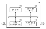
도 1은 본 발명의 실시 예에 따른 메모리 시스템의 구성을 예시적으로 설명하기 위한 블록도이다.1 is a block diagram illustrating an exemplary configuration of a memory system according to an embodiment of the present invention.
메모리 시스템(10)은 휴대폰, MP3 플레이어, 랩탑 컴퓨터, 데스크탑 컴퓨터, 게임기, TV, 차량용 인포테인먼트(in-vehicle infotainment) 시스템 등과 같은 호스트 장치에 의해서 액세스되는 데이터를 저장할 수 있다.The
메모리 시스템(10)은 호스트 장치와의 전송 프로토콜을 의미하는 호스트 인터페이스에 따라서 다양한 종류의 저장 장치들 중 어느 하나로 제조될 수 있다. 예를 들면, 메모리 시스템(10)은 SSD, MMC, eMMC, RS-MMC, micro-MMC 형태의 멀티 미디어 카드(multimedia card), SD, mini-SD, micro-SD 형태의 시큐어 디지털(secure digital) 카드, USB(universal storage bus) 저장 장치, UFS(universal flash storage) 장치, PCMCIA(personal computer memory card international association) 카드 형태의 저장 장치, PCI(peripheral component interconnection) 카드 형태의 저장 장치, PCI-E(PCI express) 카드 형태의 저장 장치, CF(compact flash) 카드, 스마트 미디어(smart media) 카드, 메모리 스틱(memory stick) 등과 같은 다양한 종류의 저장 장치들 중 어느 하나로 구성될 수 있다.The
메모리 시스템(10)은 다양한 종류의 패키지(package) 형태들 중 어느 하나로 제조될 수 있다. 예를 들면, 메모리 시스템(10)은 POP(package on package), SIP(system in package), SOC(system on chip), MCP(multi chip package), COB(chip on board), WFP(wafer-level fabricated package), WSP(wafer-level stack package) 등과 같은 다양한 종류의 패키지 형태들 중 어느 하나로 제조될 수 있다.The
메모리 시스템(10)은 컨트롤러(100) 및 비휘발성 메모리 장치(200)를 포함할 수 있다. 컨트롤러(100)는 컨트롤 유닛(110) 및 랜덤 액세스 메모리(120)를 포함할 수 있다.The
컨트롤 유닛(110)은 마이크로 컨트롤 유닛(micro control unit)(MCU), 중앙 처리 장치(central processing unit)(CPU)로 구성될 수 있다. 컨트롤 유닛(110)은 호스트 장치로부터 전송된 리퀘스트를 처리할 수 있다. 컨트롤 유닛(110)은, 리퀘스트를 처리하기 위해서, 랜덤 액세스 메모리(120)에 로딩된 코드 형태의 명령(instruction) 또는 알고리즘, 즉, 펌웨어(FW)를 구동하고, 내부의 기능 블록들 및 비휘발성 메모리 장치(200)를 제어할 수 있다.The
랜덤 액세스 메모리(120)는 동적 랜덤 액세스 메모리(DRAM) 또는 정적 랜덤 액세스 메모리(SRAM)와 같은 랜덤 액세스 메모리로 구성될 수 있다. 랜덤 액세스 메모리(120)는 컨트롤 유닛(110)에 의해서 구동되는 펌웨어(FW)를 저장할 수 있다. 또한, 랜덤 액세스 메모리(120)는 펌웨어(FW)의 구동에 필요한 데이터, 예를 들면, 메타 데이터를 저장할 수 있다. 즉, 랜덤 액세스 메모리(120)는 컨트롤 유닛(110)의 동작 메모리(working memory)로서 동작할 수 있다.The
비휘발성 메모리 장치(200)는 낸드(NAND) 플래시 메모리 장치, 노어(NOR) 플래시 메모리 장치, 강유전체 커패시터를 이용한 강유전체 램(ferroelectric random access memory: FRAM), 티엠알(tunneling magneto-resistive: TMR) 막을 이용한 마그네틱 램(magnetic random access memory: MRAM), 칼코겐 화합물(chalcogenide alloys)을 이용한 상 변화 램(phase change random access memory: PCRAM), 전이금속 산화물(transition metal oxide)을 이용한 저항성 램(resistive random access memory: RERAM) 등과 같은 다양한 형태의 비휘발성 메모리 장치들 중 어느 하나로 구성될 수 있다.The
비휘발성 메모리 장치(200)는 메모리 셀 어레이(도 15의 210)를 포함할 수 있다. 메모리 셀 어레이에 포함된 메모리 셀들은 동작의 관점에서 또는 물리적(또는 구조적) 관점에서 계층적인 메모리 셀 집합 또는 메모리 셀 단위로 구성될 수 있다. 예를 들면, 동일한 워드 라인에 연결되며, 동시에 읽혀지고 쓰여지는(또는 프로그램되는) 메모리 셀들은 페이지로 구성될 수 있다. 이하에서, 설명의 편의를 위해서, 페이지로 구성되는 메모리 셀들을 "페이지"라고 칭할 것이다. 또한, 동시에 삭제되는 메모리 셀들은 메모리 블록으로 구성될 수 있다. 메모리 셀 어레이는 복수의 메모리 블록들을 포함하고, 메모리 블록들 각각은 복수의 페이지들을 포함할 수 있다. 본 명세서에서, 복수의 메모리 블록들(Blk0 내지 Blkn)은 각각 4개의 페이지들을 포함한다고 가정한다.The
컨트롤러(100)는 호스트 장치의 리퀘스트에 대응하는 동작이 비휘발성 메모리 장치(200)에서 수행되도록 제어할 수 있다. 구체적으로, 리퀘스트에 대응하는 커맨드를 생성하여 비휘발성 메모리 장치(200)로 전송하고, 비휘발성 메모리 장치(200)에서 해당 동작이 수행되도록 제어할 수 있다. 리퀘스트에 대응하는 동작은 데이터의 쓰기 동작, 읽기 동작 등일 수 있다.The
실시 예에 따라, 하나의 메모리 시스템(10)은 서로 다른 논리적 영역을 갖는 복수의 공간으로 나누어 사용될 수 있다. 예시적으로, 복수개의 가상 시스템이 하나의 메모리 시스템(10)을 공유하여 사용할 수 있다. 복수의 가상 시스템은 물리적으로 분리된 시스템이거나, 워크로드의 성격에 따라 논리적으로 분리된 영역일 수 있다. 도시된 바와 같이, 하나의 메모리 시스템(10)을 공유하는 복수의 가상 시스템을 호스트 장치(20_0) 내지 호스트 장치(20_m)으로 예를 들어 설명한다. According to an embodiment, one
저장 매체를 포함하는 메모리 시스템(10)을 공유하는 복수의 호스트 장치들(20_0 내지 20_m) 각각은 서로 다른 성격의 워크로드를 가질 수 있다. 예를 들어, 호스트 장치(20_0)으로부터 출력된 요청에 대응하여 비휘발성 메모리 장치(200)에 저장된 데이터는 읽기 요청의 비율이 대다수이고, 호스트 장치(20_1)로부터 출력된 요청에 대응하여 저장된 데이터는 쓰기 요청의 비율이 대다수일 수 있다. 이러한 경우 호스트 장치(20_1)에 대응하는 데이터의 업데이트 횟수가 많을 수 있다. 이렇게 워크로드 특성이 다른 복수의 호스트 장치들(20_0 내지 20_m)이 하나의 메모리 시스템(10)을 사용하는 경우 저장된 데이터 또는 데이터가 저장된 메모리 블록에 대한 관리 역시 구분하여 적용할 필요성이 존재한다.Each of the plurality of host devices 20_0 to 20_m sharing the
도 2는 도 1의 랜덤 액세스 메모리에서 구동되는 소프트웨어를 예시적으로 설명하기 위한 도면이다. 도 1 및 도 2를 참조하여 플래시 변환 계층을 구동하는 예를 설명한다.FIG. 2 is a diagram for exemplarily explaining software driven in the random access memory of FIG. 1. An example of driving the flash conversion layer will be described with reference to FIGS. 1 and 2.
상술한 바와 같이, 컨트롤 유닛(110)은 메모리 블록 단위로 소거 동작을 제어하고, 페이지 단위로 읽기 또는 프로그램 동작을 제어할 수 있다. 비휘발성 메모리 장치(200)는 덮어쓰기(overwrite)가 불가능하기 때문에, 컨트롤 유닛(110)은 데이터가 저장된 메모리 셀에 새로운 데이터를 저장하기 위해서 소거 동작을 선행할 수 있다.As described above, the
컨트롤 유닛(110)은 이러한 비휘발성 메모리 장치(200) 고유의 동작을 제어하고, 호스트 장치들(20)에 장치 호환성을 제공하기 위해서 플래시 변환 계층(flash translation layer)(FTL)이라 불리는 펌웨어 또는 소프트웨어를 구동할 수 있다. 이러한 플래시 변환 계층(FTL)의 구동을 통해서, 데이터 저장 장치는 호스트 장치들(20)에 하드 디스크와 같은 일반적인 데이터 저장 장치로 인식될 수 있다.The
랜덤 액세스 메모리(120)에 로딩된 플래시 변환 계층(FTL)은 여러 기능을 수행하기 위한 모듈들과, 모듈의 구동에 필요한 메타 데이터로 구성될 수 있다. 도 2를 참조하여 예를 들면, 플래시 변환 계층(FTL)은 어드레스 맵핑 테이블(MPT), 가비지 컬렉션 모듈(GCM), 웨어-레벨링 모듈(미도시), 배드 블록 관리 모듈(미도시) 등을 포함할 수 있다.The flash translation layer (FTL) loaded in the
호스트 장치들(20)이 데이터 저장 장치를 액세스하는 경우(예를 들면, 읽기 또는 쓰기 동작을 요청하는 경우), 호스트 장치들(20)은 논리 어드레스(logical address)를 데이터 저장 장치로 제공할 수 있다. 플래시 변환 계층(FTL)은 제공된 논리 어드레스를 비휘발성 메모리 장치(200)의 물리 어드레스(physical address)로 변환하고, 변환된 물리 어드레스를 참조하여 요청된 동작을 수행할 수 있다. 이러한 어드레스 변환 동작을 위해서 어드레스 변환 데이터, 즉, 어드레스 맵핑 테이블(MPT)은 플래시 변환 계층(FTL)에 포함될 수 있다.When the
가비지 컬렉션 모듈(GCM)은 조각난 데이터들이 저장된 메모리 블록들을 관리할 수 있다. 앞서 설명된 바와 같이, 비휘발성 메모리 장치(200)는 덮어쓰기가 불가능하고, 프로그램 단위보다 소거 단위가 더 클 수 있다. 그러한 이유로, 비휘발성 메모리 장치(200)는 저장 공간이 일정한 한계에 다다르면 물리적으로 서로 상이한 위치에 분산되어 있는 유효 데이터를 한 곳으로 모으는 작업을 필요로 할 수 있다. 가비지 컬렉션 모듈(GCM)은 복수의 쓰기 동작들과 복수의 소거 동작들을 수행하여 조각난 유효 데이터를 수집 영역으로 모으는 작업을 수행할 수 있다. 본 발명의 실시 예에 따라 유효 데이터의 가비지 컬렉션 동작이 수행되는 과정은 도 4 내지 도 9b를 참조하여 자세히 설명한다.The garbage collection module (GCM) may manage memory blocks in which fragmented data is stored. As described above, the
웨어-레벨링 모듈은 비휘발성 메모리 장치(200)의 페이지들 또는 메모리 블록들에 대한 마모도(wear-level)를 관리할 수 있다. 프로그램 그리고 소거 동작에 의해서 비휘발성 메모리 장치(200)의 메모리 셀들은 노화(aging)될 수 있다. 노화된 메모리 셀, 즉, 마모된 메모리 셀은 결함을 야기할 수 있다. 웨어-레벨링 모듈은 특정 메모리 블록이 다른 메모리 블록들보다 빨리 마모되는 것을 방지하기 위해서 메모리 블록들 각각의 프로그램-소거 횟수(program-erase count)가 평준화되도록 관리할 수 있다.The wear-leveling module may manage wear-levels of pages or memory blocks of the
배드 블록 관리 모듈은 비휘발성 메모리 장치(200)의 메모리 블록들 중에서 결함이 발생된 메모리 블록을 관리할 수 있다. 앞서 설명된 바와 같이, 마모된 메모리 셀은 결함이 발생될 수 있다. 결함이 발생된 메모리 셀에 저장된 데이터는 정상적으로 읽혀질 수 없다. 또한, 결함이 발생된 메모리 셀에는 데이터가 정상적으로 저장되지 않을 수 있다. 배드 블록 관리 모듈은 결함이 발생된 메모리 셀을 포함하는 메모리 블록이 사용되지 않도록 관리할 수 있다.The bad block management module may manage a defective memory block among memory blocks of the
도 3a는 각각의 논리 어드레스 그룹들에 포함되는 논리 어드레스 범위를 예시적으로 설명하기 위한 도면이다. 이하에서, 도 1 및 도 3을 참조하여 메모리 시스템(10)에 적용되는 네임스페이스의 예를 설명한다.3A is a diagram for illustratively explaining a logical address range included in each logical address group. Hereinafter, an example of a namespace applied to the
기업의 저장 장치 시장에서, 다중 경로와 가상화(virtualization)는 저장 장치 내에서 복수의 호스트 개체에서 데이터를 공유 하기 위한 중요한 요소에 해당한다. 상기 데이터 공유의 요소는 필요 시 복수의 호스트에 데이터를 액세스하는 것을 가능하게 한다In the enterprise storage market, multipathing and virtualization are important factors for sharing data among multiple host objects within a storage device. The element of data sharing makes it possible to access data on multiple hosts when needed.
본 발명의 실시 예에 따른 메모리 시스템(10)은 네임스페이스 기능을 지원할 수 있다. 여기서, "네임스페이스"는 논리 블록들로 포맷될 수 있는 비휘발성 메모리 장치(200)의 양(quantity)으로 정의할 수 있고, 각각의 네임 스페이스는 서도 다른 논리 어드레스 그룹(LAG)에 대응할 수 있고, 각각의 논리 어드레스 그룹(LAG)은 서로 다른 논리 어드레스(Logical Address, LA) 범위를 갖는 논리 블록들의 컬렉션(collection)이다. "네임스페이스 기능"은 하나의 물리적 장치로부터 복수의 논리적 장치들(예를 들어, 호스트 장치들(20_0 내지 20_m))을 제공하는 기능을 나타낸다. 구체적으로, 네임스페이스 기능은 메모리 시스템(10)을 복수의 네임스페이스들로 나누고, 각 네임스페이스 별로 고유한 논리 어드레스를 할당하는 기법이다. The
메모리 시스템(10)은 멀티 네임스페이스를 관리할 수 있고, 이에 따라 멀티 네임스페이스 기능을 제공한다고 지칭할 수 있다. 구체적으로, 메모리 시스템(10)은 복수의 네임스페이스들(또는, 복수의 논리 어드레스 그룹)을 동적으로 생성할 수 있고, 또한, 생성된 복수의 네임스페이스들 중 일부 네임스페이스를 동적으로 삭제할 수 있다. 예를 들어, 메모리 시스템(10)은 NVMe SSD(Non-Volatile Memory Express Solid State Drive) 장치일 수 있다. 본 명세서에서, 복수의 논리 어드레스 그룹들(LAG0 내지 LAG3)은 멀티 네임스페이스를 의미할 수 있다.The
도시된 바와 같이, 메모리 시스템(10)은 4개의 논리 어드레스 그룹들(LAG0 내지 LAG3)을 관리할 수 있다. 각각의 논리 어드레스 그룹들(LAG0 내지 LAG3)은 서로 다른 논리 어드레스 범위를 포함할 수 있다. 예시적으로, 논리 어드레스 그룹(LAG0)은 논리 어드레스(LA0) 내지 논리 어드레스(LA499)의 범위의 논리 어드레스를 포함할 수 있다. 논리 어드레스 그룹(LAG1)은 논리 어드레스(LA500) 내지 논리 어드레스(LA749)의 범위의 논리 어드레스를 포함할 수 있다. 논리 어드레스 그룹(LAG2)는 논리 어드레스(LA750) 내지 논리 어드레스(LA999)의 범위의 논리 어드레스를 포함할 수 있다. 논리 어드레스 그룹(LAG3)은 논리 어드레스(LA1000) 내지 논리 어드레스(LA1999)의 범위의 논리 어드레스를 포함할 수 있다. 즉, 논리 어드레스 그룹들(LAG0 내지 LAG3)은 각각 500, 250, 250, 1000개의 논리 어드레스를 포함할 수 있다. 각각의 논리 어드레스 그룹들(LAG0 내지 LAG3)에 대응하는 논리 어드레스 범위는 호스트 장치들(20_0 내지 20_m)의 워크로드 특성에 따라서 가변적으로 설정될 수 있다.As shown, the
도 3b는 맵핑 테이블에 저장되는 정보를 예시적으로 설명하기 위한 도면이다.3B is a diagram for illustratively describing information stored in a mapping table.
상술한 바와 같이, 플래시 변환 계층(FTL)은 제공된 논리 어드레스를 비휘발성 메모리 장치(200)의 물리 어드레스(physical address)로 변환하고, 변환된 물리 어드레스를 참조하여 요청된 동작을 수행할 수 있다. 이러한 어드레스 변환 동작을 위해서 어드레스 변환 데이터, 즉, 어드레스 맵핑 테이블(MPT)은 플래시 변환 계층(FTL)에 포함될 수 있다.As described above, the flash translation layer (FTL) may convert the provided logical address to a physical address of the
실시 예에 따라, 맵핑 테이블(MPT)은 물리 어드레스(Physical Address, PA), 논리 어드레스(LA) 및 논리 어드레스 그룹(LAG)에 대한 정보를 포함할 수 있다. 물리 어드레스(PA)는 블록 어드레스(ADD_Blk) 및 페이지 어드레스(ADD_PG)를 포함할 수 있다. 예시적으로, 블록 어드레스(ADD_Blk) 0을 갖는 메모리 블록(이하, "Blk0") 및 블록 어드레스(ADD_Blk) 1을 갖는 메모리 블록(이하, "Blk1")에 대응하는 논리 어드레스(LA) 및 논리 어드레스 그룹(LAG)이 도시되었다.According to an embodiment, the mapping table MPT may include information about a physical address (PA), a logical address (LA), and a group of logical addresses (LAG). The physical address PA may include a block address ADD_Blk and a page address ADD_PG. For example, a logical address LA and a logical address corresponding to a memory block having a block address (ADD_Blk) 0 (hereinafter, "Blk0") and a memory block having a block address (ADD_Blk) 1 (hereinafter, "Blk1"). The group (LAG) is shown.
맵핑 테이블(MPT)에는 메모리 블록(Blk0)의 페이지 어드레스(ADD_PG) 0 내지 2을 갖는 페이지들에는 각각 400 내지 402의 논리 어드레스(LA)에 대응하는 데이터가 저장되었다는 정보와, 이를 포함하는 논리 어드레스 그룹(LAG)인 논리 어드레스 그룹(LAG0)에 대한 정보가 저장된다. 또한, 메모리 블록(Blk0)의 페이지 어드레스(ADD_PG) 3을 갖는 페이지에는 논리 어드레스(LA) 0에 대응하는 데이터가 저장되었다는 정보와, 이를 포함하는 논리 어드레스 그룹(LAG)인 논리 어드레스 그룹(LAG0)에 대한 정보가 저장된다. 마찬가지로, 메모리 블록(Blk1)의 페이지 어드레스(ADD_PG) 0 내지 3을 갖는 페이지들에는 각각 1000, 1001, 800 및 801의 논리 어드레스(LA)에 대응하는 데이터가 저장되었다는 정보와, 페이지들 각각에 대응하는 논리 어드레스 그룹들(LAG3, LAG3, LAG2, LAG2)에 대한 정보가 저장되었다.In the mapping table MPT, information corresponding to logical addresses LA of 400 to 402 is stored in
도시되지는 않았으나, 실시 예에 따라 맵핑 테이블(MPT)에는 비휘발성 메모리 장치(200)에 저장된 데이터가 유효 데이터인지 또는 무효 데이터인지 여부가 더 저장될 수 있다. 예를 들어, 메모리 블록(Blk0)의 페이지 어드레스(ADD_PG) 0을 갖는 비휘발성 메모리 장치(200) 내의 위치에 저장된 데이터가 유효 데이터, 즉 가장 최근에 업데이트된 데이터인지 또는 무효 데이터, 즉 논리 어드레스(LA) 400에 대응하는 새로운 데이터가 비휘발성 메모리 장치(200)의 다른 위치에 저장되었는지 여부를 포함할 수 있다.Although not illustrated, the mapping table MPT may further store whether the data stored in the
실시 예에 따라, 컨트롤러(100)는 맵핑 테이블(MPT)을 참조하여 데이터가 유효 데이터인지 또는 무효 데이터인지 여부를 판단할 수 있다. 예를 들어, 요구되는 데이터와 동일한 논리 어드레스를 갖는 데이터가 비휘발성 메모리 장치(200)의 다른 영역에 저장되어 있는지 여부를 맵핑 테이블(MPT)을 참조하여 판단할 수 있고, 이에 기초하여 해당 영역에 저장된 데이터가 유효 데이터인지 또는 무효 데이터인지 여부를 판단할 수 있다.According to an embodiment, the
도 4는 도 2의 가비지 컬렉션 모듈에 의해서 수행되는 가비지 컬렉션 동작을 설명하기 위한 도면이다.FIG. 4 is a diagram illustrating a garbage collection operation performed by the garbage collection module of FIG. 2.
데이터가 쓰여지지 않은 메모리 블록, 즉 소거된 메모리 블록은 빈(empty) 블록으로 정의될 수 있고, 소거된 상태인 빈 블록은 빈 페이지를 포함할 수 있다. 데이터가 쓰여진 메모리 블록은 사용된 블록으로 정의될 수 있다. 사용된 블록은 유효한(valid) 데이터가 저장된 페이지(이하, 유효 페이지라 칭함) 및 무효한(invalid) 데이터가 저장된 페이지(이하, 무효 페이지라 칭함) 중 적어도 하나를 포함할 수 있다. 사용된 메모리 블록들 중에서, 가비지 컬렉션 동작의 대상으로 선정된 메모리 블록, 즉, 가비지 컬렉션이 수행될 메모리 블록은 희생(victim) 블록으로 정의될 수 있다. 가비지 컬렉션의 수행으로 희생 블록의 유효 페이지에 저장된 데이터가 백업될 블록은 타겟(target) 블록(Blk_T)로 정의될 수 있다. A memory block in which data is not written, that is, an erased memory block may be defined as an empty block, and an empty block in an erased state may include an empty page. The memory block to which data is written can be defined as a used block. The used block may include at least one of a page in which valid data is stored (hereinafter referred to as a valid page) and a page in which invalid data is stored (hereinafter referred to as an invalid page). Among the used memory blocks, a memory block selected as a target of a garbage collection operation, that is, a memory block to be garbage collected may be defined as a victim block. A block in which data stored in the valid page of the victim block is to be backed up by performing garbage collection may be defined as a target block (Blk_T).
도 4를 참조하면, 희생 블록은 메모리 블록(Blk0) 및 메모리 블록(Blk1)로 설정되었다고 가정한다. 희생 블록인 메모리 블록(Blk0)의 페이지들(PG1~PG4) 중에서 유효 페이지(PG4)는 타겟 블록(Blk_T)의 빈 페이지(PG1)에 복사될 수 있다. 또한, 다른 희생 블록인 메모리 블록(Blk1)의 페이지들(PG1 내지 PG4) 중에서 무효 페이지들(PG2 및 PG3)을 제외한 유효 페이지들(PG0 및 PG1)은 타겟 블록(Blk_T)의 빈 페이지들(PG2 및 PG3)에 각각 복사될 수 있다. 유효 페이지가 복사된 이후에, 희생 블록들(Blk0 및 Blk1) 각각은 삭제되고, 빈 블록들로 변경될 수 있다.Referring to FIG. 4, it is assumed that the victim block is set as the memory block Blk0 and the memory block Blk1. Among the pages PG1 to PG4 of the memory block Blk0, which is the victim block, the valid page PG4 may be copied to an empty page PG1 of the target block Blk_T. In addition, valid pages PG0 and PG1 except invalid pages PG2 and PG3 among pages PG1 to PG4 of the memory block Blk1, which are other victim blocks, are empty pages PG2 of the target block Blk_T. And PG3). After the valid page is copied, each of the sacrificial blocks Blk0 and Blk1 is deleted and can be changed into empty blocks.
메모리 블록(Blk0)의 페이지들(PG0 내지 PG3)에는 모두 논리 어드레스 그룹(LAG0)에 포함되는 논리 어드레스에 대응되는 데이터가 저장되어 있고, 메모리 블록(Blk1)의 페이지들(PG0 내지 PG3)에는 각각 논리 어드레스 그룹(LAG3), 논리 어드레스 그룹(LAG3), 논리 어드레스 그룹(LAG2) 및 논리 어드레스 그룹(LAG2)에 포함되는 논리 어드레스들에 대응하는 데이터가 저장되어 있다. 이 때, 가비지 컬렉션(GC) 동작을 수행하게 되면, 메모리 블록(Blk0)의 페이지(PG3)에 저장된 유효 데이터와, 메모리 블록(Blk1)의 페이지들(PG0 및 PG1)에 저장된 유효 데이터가 타겟 블록(Blk_T)으로 백업 되고, 결과적으로 타겟 블록(Blk_T)의 각각의 페이지들(PG0 내지 PG2)에는 논리 어드레스 그룹(LAG0), 논리 어드레스 그룹(LAG3), 및 논리 어드레스 그룹(LAG3)에 포함되는 논리 어드레스에 대응하는 유효 데이터가 저장된다.Data corresponding to the logical address included in the logical address group LAG0 is stored in the pages PG0 to PG3 of the memory block Blk0, and the pages PG0 to PG3 of the memory block Blk1 are respectively Data corresponding to logical addresses included in the logical address group LAG3, the logical address group LAG3, the logical address group LAG2, and the logical address group LAG2 is stored. At this time, when the garbage collection (GC) operation is performed, valid data stored in pages PG3 of the memory block Blk0 and valid data stored in pages PG0 and PG1 of the memory block Blk1 are target blocks. Logical address group LAG0, logical address group LAG3, and logical address group LAG3 included in each page PG0 to PG2 of the target block Blk_T. Valid data corresponding to the address is stored.
가비지 컬렉션(GC) 동작은 유효 페이지를 희생 블록으로부터 타겟 블록(Blk_T)으로 복사하는 동작, 즉, 쓰기 동작과, 희생 블록을 소거하는 동작을 수반하기 때문에 컨트롤러의 리소스를 많이 소모하게 되고, 긴 동작 시간을 필요로 할 수 있다. 특히, 복수의 호스트 장치들이 메모리 시스템을 공유하는 경우, 서로 다른 워크로드 특성을 가진 데이터(예를 들어, 서로 다른 호스트 장치들로부터 요청된 데이터)가 동일한 메모리 블록에 저장되는 경우, 동일한 메모리 블록에 저장된 데이터의 업데이트 시점이 상이할 수 있고, 유효 데이터와 무효 데이터가 공존할 가능성이 높아질 수 있다. 따라서, 가비지 컬렉션(GC) 동작의 대상인 희생 블록의 수가 증가하거나, 가비지 컬렉션(GC) 동작의 수행 횟수가 증가하거나, 가비지 컬렉션(GC)의 수행 시간이 증가할 수 있고, 이에 따라 시스템의 성능이 하락할 수 있다.Since the garbage collection (GC) operation involves an operation of copying an effective page from the victim block to the target block (Blk_T), that is, a write operation and an operation of erasing the victim block, a controller consumes a lot of resources and has a long operation. It may take time. In particular, when a plurality of host devices share a memory system, data having different workload characteristics (for example, data requested from different host devices) is stored in the same memory block, in the same memory block The update time of the stored data may be different, and the possibility that valid data and invalid data can coexist may increase. Accordingly, the number of sacrificial blocks targeted for the garbage collection (GC) operation may increase, the number of times the garbage collection (GC) operation is performed may increase, or the execution time of the garbage collection (GC) operation may increase, and accordingly, the performance of the system may increase. It can fall.
가비지 컬렉션(GC) 동작이 발생되는 시기 또는 가비지 컬렉션(GC) 동작에 소요되는 시간을 최적화시키면, 메모리 시스템의 동작 속도는 향상될 수 있다. 또는, 가비지 컬렉션(GC) 동작이 수행되는 양, 즉, 가비지 컬렉션(GC) 수행량 또는 처리량(throughput)을 최적화시키면, 메모리 시스템의 동작 속도는 향상될 수 있다.When the garbage collection (GC) operation occurs or the time required for the garbage collection (GC) operation is optimized, the operation speed of the memory system may be improved. Alternatively, if the amount of garbage collection (GC) operation is performed, that is, the garbage collection (GC) throughput or throughput is optimized, the operation speed of the memory system may be improved.
도 5는 복수의 논리 어드레스 그룹들에 대응하는 유효 데이터가 저장된 희생 블록을 예시적으로 보여주는 도면이다.5 is a diagram exemplarily showing a victim block in which valid data corresponding to a plurality of logical address groups is stored.
실시 예에 따라, 내부 백업 동작의 대상인 희생 블록 및 희생 블록의 유효 데이터가 백업되는 타겟 블록은 복수의 메모리 블록들을 포함하는 슈퍼 블록 단위로 설정될 수 있다. 슈퍼 블록은 복수의 비휘발성 메모리 장치들에 걸쳐 형성될 수 있다. 슈퍼 블록은 복수의 비휘발성 메모리 장치들 각각에 포함된 하나 이상의 메모리 블록들로 구성될 수 있다.According to an embodiment, the target block to which the valid data of the victim block and the victim block that is the target of the internal backup operation are backed up may be set in units of super blocks including a plurality of memory blocks. The super block may be formed across a plurality of nonvolatile memory devices. The super block may be composed of one or more memory blocks included in each of the plurality of nonvolatile memory devices.
이하에서, 희생 블록 및 타겟 블록은 슈퍼 블록 단위로 설명되고, 각각의 희생 블록 및 타겟 블록은 4개의 메모리 블록들을 포함하고, 각각의 메모리 블록들은 4개의 페이지들(PG0 내지 PG3)을 포함한다고 가정한다.Hereinafter, it is assumed that the sacrificial block and the target block are described in units of super blocks, each sacrificial block and the target block include 4 memory blocks, and each memory block includes 4 pages PG0 to PG3. do.
도 1 및 도 5를 참조하면, 희생 블록(VSB_0)은 4개의 희생 메모리 블록들(VB_0 내지 VB_3)을 포함하고, 각각의 희생 메모리 블록들에 포함되는 페이지들(PG0 내지 PG3)에는 데이터가 모두 저장되어 있다. 유효 데이터는 논리 어드레스에 대응하는 최신의 데이터를 의미할 수 있다. 즉, 특정 논리 어드레스에 대응되는 복수의 데이터가 비휘발성 메모리 장치(200)에 저장된 경우, 가장 최근에 저장된 데이터가 유효 데이터가 되고, 유효 데이터를 제외한 데이터는 무효 데이터로 정의될 수 있다. 실시 예에 따라, 컨트롤러(100)는 랜덤 액세스 메모리(120) 또는 비휘발성 메모리 장치(200)에 저장된 맵핑 테이블을 참조하여, 희생 블록에 저장된 데이터가 유효 데이터인지 또는 무효 데이터인지 여부에 대한 정보를 획득할 수 있다.1 and 5, the sacrificial block VSB_0 includes four sacrificial memory blocks VB_0 to VB_3, and all of the pages PG0 to PG3 included in each sacrificial memory block have data. Is stored. The valid data may mean the latest data corresponding to the logical address. That is, when a plurality of data corresponding to a specific logical address is stored in the
희생 메모리 블록(VB_0)에는 논리 어드레스 그룹(LAG0)에 포함되는 논리 어드레스에 대응하는 유효 데이터가 3개의 페이지들(PG0, PG1, PG2)에 저장되어 있고, 희생 메모리 블록(VB_1)에는 논리 어드레스 그룹(LAG3)에 포함되는 논리 어드레스에 대응하는 유효 데이터가 2개의 페이지들(PG2, PG3)에 저장되어 있다. 또한, 희생 메모리 블록(VB_2)에는 논리 어드레스 그룹(LAG0)에 포함되는 논리 어드레스에 대응하는 유효 데이터가 2개의 페이지들(PG0, PG1)에 저장되어 있고, 논리 어드레스 그룹(LAG2)에 포함되는 논리 어드레스에 대응하는 유효 데이터가 페이지(PG2)에 저장되어 있다. 희생 메모리 블록(VB_3)에는 논리 어드레스 그룹(LAG1)에 포함되는 논리 어드레스에 대응하는 유효 데이터가 2개의 페이지들(PG0, PG1)에 저장되어 있다.In the victim memory block VB_0, valid data corresponding to the logical address included in the logical address group LAG0 is stored in three pages PG0, PG1, and PG2, and the logical address group is provided in the victim memory block VB_1. Valid data corresponding to the logical address included in (LAG3) is stored in two pages PG2 and PG3. Also, in the victim memory block VB_2, valid data corresponding to the logical address included in the logical address group LAG0 is stored in two pages PG0 and PG1, and the logic included in the logical address group LAG2 Valid data corresponding to the address is stored in the page PG2. In the sacrificial memory block VB_3, valid data corresponding to the logical address included in the logical address group LAG1 is stored in two pages PG0 and PG1.
내부 백업 동작의 대상인 희생 블록(VSB_0)에 포함되는 페이지들 중 10개의 페이지들에 유효 데이터가 저장되어 있고, 논리 어드레스 그룹(LAG0) 내지 논리 어드레스 그룹(LAG3) 각각에 포함되는 논리 어드레스에 대응하는 유효 데이터는 5개, 2개, 1개, 2개가 존재한다. 이후 진행되는 내부 백업 동작(예를 들어, 가비지 컬렉션)에서 10개의 유효 데이터는 타겟 블록의 특정 영역에 저장될 것이다.Valid data is stored in 10 pages among the pages included in the victim block VSB_0, which is the target of the internal backup operation, and corresponds to logical addresses included in each of the logical address group LAG0 to the logical address group LAG3. There are 5, 2, 1, and 2 valid data. In the subsequent internal backup operation (eg, garbage collection), 10 valid data will be stored in a specific area of the target block.
도 6은 본 발명의 실시 예에 따라, 도 5의 희생 블록(VSB_0)에 저장된 유효 데이터가 2개의 타겟 블록들(TSB_0, TSB_1)에 백업되는 경우를 설명하기 위한 도면이고, 도 7은 도 6의 실시 예를 시계열적으로 설명하기 위한 순서도이다. 이하에서, 도 1, 도 5 내지 도 7을 참조하여 본 발명의 실시 예에 따라 유효 데이터가 2개의 타겟 블록들(TSB_0, TSB_1)에 저장되는 과정을 설명한다.FIG. 6 is a diagram for explaining a case in which valid data stored in the victim block VSB_0 of FIG. 5 is backed up to two target blocks TSB_0 and TSB_1 according to an embodiment of the present invention. It is a flow chart for explaining an embodiment of the time series. Hereinafter, a process in which valid data is stored in two target blocks TSB_0 and TSB_1 according to an embodiment of the present invention will be described with reference to FIGS. 1 and 5 to 7.
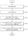
S110 단계에서, 컨트롤 유닛(110)은 도 5의 희생 블록(VSB_0)을 선택할 수 있다. 희생 블록(VSB_0)은 4개의 메모리 블록들을 포함하는 슈퍼 블록 단위로 설정될 수 있다. 희생 블록(VSB_0)의 10개의 페이지들에 유효 데이터가 저장되어 있다.In step S110, the
S120 단계에서, 컨트롤 유닛(110)은 도6의 타겟 블록들(TSB_0, TSB_1)을 선택할 수 있다. 타겟 블록들(TSB_0, TSB_1)은 각각이 4개의 메모리 블록들을 포함하는 슈퍼 블록 단위로 설정될 수 있다.In step S120, the
S130 단계에서, 컨트롤 유닛(110)은 타겟 블록들(TSB_0, TSB_1) 각각에 논리 어드레스 그룹들(LAG0~LAG3) 중 적어도 하나의 논리 어드레스 그룹을 맵핑할 수 있다.In step S130, the
예를 들어, 컨트롤 유닛(110)은 논리 어드레스 그룹들(LAG0~LAG3) 중, 희생 블록(VSB_0)에 저장된 유효 데이터의 논리 어드레스들을 가장 많이 포함하는 논리 어드레스 그룹(LAG0)을 결정할 수 있다. 컨트롤 유닛(110)은 타겟 블록들(TSB_0, TSB_1) 중 어느 하나의 타겟 블록, 예를 들어, 타겟 블록(TSB_0)에 논리 어드레스 그룹(LAG0)을 맵핑할 수 있다. 컨트롤 유닛(110)은 타겟 블록들(TSB_0, TSB_1) 중 다른 하나의 타겟 블록(TSB_1)에 논리 어드레스 그룹들(LAG0~LAG3) 중 논리 어드레스 그룹(LAG0)을 제외한 나머지 논리 어드레스 그룹들(LAG1~LAG3)을 맵핑할 수 있다.For example, the
S140 단계에서, 컨트롤 유닛(110)은 논리 어드레스 그룹들(LAG0~LAG3) 중에서, 희생 블록(VSB_0)에 저장된 제1 유효 데이터의 논리 어드레스를 포함하는 제1 논리 어드레스 그룹을 판단할 수 있다.In step S140, the
S150 단계에서, 컨트롤 유닛(110)은 제1 유효 데이터를 타겟 블록들(TSB_0, TSB_1) 중에서 제1 논리 어드레스 그룹에 맵핑된 제1 타겟 블록에 백업할 수 있다. 따라서, 컨트롤 유닛(110)은 논리 어드레스 그룹(LAG0)에 대응하는 유효 데이터를 타겟 블록(TSB_0)에 백업하고, 논리 어드레스 그룹들(LAG1~LAG3)에 대응하는 유효 데이터를 타겟 블록(TSB_1)에 백업할 수 있다.In step S150, the
S130 단계와 관련하여, 실시 예에 따라, 컨트롤 유닛(110)은 논리 어드레스 그룹들(LAG0~LAG3)이 가지는 오프셋 값들에 따라, 타겟 블록들(TSB_0, TSB_1) 각각에 적어도 하나의 논리 어드레스 그룹을 맵핑할 수 있다. 예를 들어, 컨트롤 유닛(110)은 논리 어드레스 그룹의 오프셋 값이 홀수인지 또는 짝수인지 여부에 따라 타겟 블록들(TSB_0, TSB_1) 각각에 적어도 하나의 논리 어드레스 그룹을 맵핑할 수 있다. 예를 들어, 컨트롤 유닛(110)은 타겟 블록(TSB_0)에 홀수 오프셋 값을 갖는 논리 어드레스 그룹(LAG1) 및 논리 어드레스 그룹(LAG3)을 맵핑하고, 타겟 블록(TSB_1)에 짝수 오프셋 값을 갖는 논리 어드레스 그룹(LAG0) 및 논리 어드레스 그룹(LAG2)을 맵핑할 수 있다.In relation to step S130, according to an embodiment, the
본 발명의 실시 예에 따르면 비휘발성 메모리 장치(200)의 내부 백업 동작의 효율이 향상될 수 있다. 특히, 복수의 호스트 장치들이 메모리 시스템(10)을 공유하는 경우, 동일한 논리 어드레스 그룹에 대응하는 데이터를 동일한 타겟 블록에 저장하게 되면 서로 다른 워크로드 특징을 가진 데이터가 동일한 메모리 블록에 저장되는 경우가 감소되고, 동일한 메모리 블록에 저장된 데이터에 대한 데이터의 업데이트 시점이 유사할 가능성이 높아진다. 따라서 메모리 블록에 유효 데이터와 무효 데이터가 공존할 가능성이 낮아지고, 결과적으로 내부 백업 동작(예를 들어, 가비지 컬렉션)의 수행 횟수가 감소하고, 수행 시간이 단축될 수 있다.According to an embodiment of the present invention, the efficiency of the internal backup operation of the
도 8은 본 발명의 실시 예에 따라, 도 5의 희생 블록(VSB_0)에 저장된 유효 데이터가 1개의 타겟 블록(TSB)에 백업되는 경우를 설명하기 위한 도면이고, 도 9는 도 8의 실시 예를 시계열적으로 설명하기 위한 순서도이다. 이하에서, 도 1, 도 5, 도 8 내지 도 9를 참조하여 본 발명의 실시 예에 따라 유효 데이터가 1개의 타겟 블록(TSB)에 저장되는 과정을 설명한다.8 is a diagram for explaining a case in which valid data stored in the victim block VSB_0 of FIG. 5 is backed up to one target block TSB according to an embodiment of the present invention, and FIG. 9 is an embodiment of FIG. 8 Is a flowchart for explaining time series. Hereinafter, a process in which valid data is stored in one target block (TSB) according to an embodiment of the present invention will be described with reference to FIGS. 1, 5, 8 to 9.
실시 예에 따라, 컨트롤 유닛(110)은 데이터의 내부 백업 동작 시에 1개의 슈퍼 블록(TSB)을 타겟 블록으로 설정할 수 있다. 즉, 4개의 메모리 블록들(TB_0, TB_1, TB_2, TB_3)을 포함하는 슈퍼 블록(TSB)을 타겟 블록으로 설정할 수 있다. 도시된 바와 같이, 타겟 블록(TSB)에 포함되는 4개의 타겟 메모리 블록들(TB_0, TB_1, TB_2, TB_3)은 서로 다른 비휘발성 메모리 장치에 위치한다고 가정한다. 타겟 메모리 블록(TB_0) 및 타겟 메모리 블록(TB_2)는 채널(CH0)에 의하여 커맨드와 데이터가 송수신되는 비휘발성 메모리 장치(MV0) 및 비휘발성 메모리 장치(MV2)에 위치하고, 타겟 메모리 블록(TB_1) 및 타겟 메모리 블록(TB_3)은 채널(CH1)에 의하여 구동되는 비휘발성 메모리 장치(MV1) 및 비휘발성 메모리 장치(MV3)에 위치한다. 또한, 비휘발성 메모리 장치(MV0) 및 비휘발성 메모리 장치(MV1)은 칩 인에이블 신호(CE0)에 의하여 구동되고, 비휘발성 메모리 장치(MV2) 및 비휘발성 메모리 장치(MV3)은 칩 인에이블 신호(CE1)에 의하여 구동된다고 가정한다. 이때, 칩 인에이블 신호(CE0)는 타겟 블록(TSB)을 구동하는 칩 인에이블 신호들(CE0, CE1) 중 가장 먼저 생성되는 칩 인에이블 신호일 수 있다.According to an embodiment, the
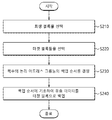
S210 단계에서, 컨트롤 유닛(110)은 희생 블록(VSB_0)을 선택할 수 있다.In step S210, the
S220 단계에서, 컨트롤 유닛(110)은 빈 블록들 중에서 희생 블록(VSB_0)에 저장된 유효 데이터가 백업되는 타겟 블록(TSB)을 선택할 수 있다.In step S220, the
S230 단계에서, 컨트롤 유닛(110)은 논리 어드레스 그룹들(LAG0~LAG3)의 백업 순서를 결정할 수 있다. 백업 순서는 각각의 논리 어드레스 그룹들(LAG0~LAG3)에 대응하는 유효 데이터가 타겟 블록(TSB)에 백업되는 순서일 수 있다. In step S230, the
구체적으로, 컨트롤 유닛(110)은 타겟 블록(TSB)을 구성하는 복수의 영역들 중 유효 데이터가 가장 먼저 백업될 제1 영역을 선택하고, 논리 어드레스 그룹들(LAG0~LAG3) 중 제1 영역에 맵핑될 제1 논리 어드레스 그룹을 선택할 수 있다. 즉, 제1 논리 어드레스 그룹은 백업 순서에서 가장 빠를 수 있다. 또한, 컨트롤 유닛(110)은 타겟 블록(TSB)을 구성하는 복수의 영역들 중 제2 영역을 선택하고, 제1 논리 어드레스 그룹을 제외한 논리 어드레스 그룹들 중 제2 영역에 맵핑될 제2 논리 어드레스 그룹을 선택할 수 있다. 즉, 제2 논리 어드레스 그룹은 백업 순서에서 제1 논리 어드레스 그룹보다 느릴 수 있다. 실시 예에 따라, 제2 논리 어드레스 그룹은 논리 어드레스 그룹들(LAG0~LAG3) 중 제1 논리 어드레스 그룹 이외의 논리 어드레스 그룹들일 수 있다.Specifically, the
실시 예에 따라, 제1 영역은 제1 칩 인에이블 신호에 의하여 구동되고, 제2 영역은 제2 칩 인에이블 신호에 의하여 구동될 수 있다. 즉, 제1 영역과 제2 영역은 서로 다른 칩 인에이블 신호들에 의하여 구동되도록 선택될 수 있다. 제1 칩 인에이블 신호는, 타겟 블록(TSB)을 구동하는 칩 인에이블 신호들 중 가장 먼저 생성되는 칩 인에이블 신호일 수 있다.According to an embodiment, the first region may be driven by the first chip enable signal, and the second region may be driven by the second chip enable signal. That is, the first region and the second region may be selected to be driven by different chip enable signals. The first chip enable signal may be a chip enable signal generated first among chip enable signals driving the target block TSB.
예를 들어, 컨트롤 유닛(110)은 타겟 블록(TSB)을 구성하는 타겟 메모리 블록들(TB_0~TB3) 중 유효 데이터가 가장 먼저 백업될 제1 영역으로 타겟 메모리 블록들(TB_0, TB_1)을 선택할 수 있다. 타겟 메모리 블록들(TB_0, TB_1)은 칩 인에이블 신호들(CE0, CE1) 중 가장 먼저 생성되는 칩 인에이블 신호(CE0)에 의해 구동되므로 제1 영역으로 선택될 수 있다. 그리고 컨트롤 유닛(110)은 논리 어드레스 그룹들(LAG0~LAG3) 중 타겟 메모리 블록들(TB_0, TB_1)에 맵핑될 제1 논리 어드레스 그룹으로 논리 어드레스 그룹(LAG0)을 선택할 수 있다. 논리 어드레스 그룹(LAG0)은 논리 어드레스 그룹들(LAG0~LAG3) 중 희생 블록(VSB_0)에 저장된 유효 데이터에 대응하는 논리 어드레스들을 가장 많이 포함하는 논리 어드레스 그룹일 수 있다. 그 결과 컨트롤 유닛(110)은 타겟 메모리 블록들(TB_0, TB_1)에 논리 어드레스 그룹(LAG0)을 맵핑할 수 있다.For example, the
다른 실시 예로서, 컨트롤 유닛(110)은 제1 논리 어드레스 그룹으로 논리 어드레스 그룹들(LAG0~LAG3) 중 기설정된 오프셋 값을 가지는 논리 어드레스 그룹을 선택할 수도 있다.As another embodiment, the
또한 컨트롤 유닛(110)은 타겟 메모리 블록들(TB_0~TB3) 중 타겟 메모리 블록들(TB_2, TB_3)을 백업 순서에서 제1 영역보다 느린 제2 영역으로 선택할 수 있다. 타겟 메모리 블록들(TB_2, TB_3)은 칩 인에이블 신호(CE1)에 의해 구동될 수 있다. 그리고 컨트롤 유닛(110)은 타겟 메모리 블록들(TB_2, TB_3)에 맵핑될 제2 논리 어드레스 그룹으로 논리 어드레스 그룹들(LAG1~LAG3)을 선택할 수 있다. 컨트롤 유닛(110)은 타겟 메모리 블록들(TB_2, TB_3)에 논리 어드레스 그룹들(LAG1~LAG3)을 맵핑할 수 있다.In addition, the
S240 단계에서, 컨트롤 유닛(110)은 백업 순서에 기초하여 희생 블록(VSB_0)에 저장된 유효 데이터 중 선택된 유효 데이터를 타겟 블록(TSB)으로 백업할 수 있다. 컨트롤 유닛(110)은 S230 단계에서 맵핑된 바에 따라, 타겟 메모리 블록들(TB_0, TB_1)에 논리 어드레스 그룹(LAG0)에 대응하는 유효 데이터를 백업하고, 타겟 메모리 블록들(TB_2, TB_3)에 논리 어드레스 그룹들(LAG1~LAG3)에 대응하는 유효 데이터를 백업할 수 있다.In step S240, the
본 발명의 실시 예에 따르면, 비휘발성 메모리 장치(200)의 내부 백업 동작의 효율이 향상될 수 있다. 특히, 복수의 호스트 장치들이 메모리 시스템(10)을 공유하는 경우, 동일한 논리 어드레스 그룹에 포함되는 논리 어드레스에 대응하는 데이터를 동일한 영역(예를 들어, 동일한 칩 인에이블 신호에 의하여 구동되는 영역)에 저장하게 되면 서로 다른 워크로드 특징을 가진 데이터가 동일한 메모리 블록에 저장되는 경우가 감소되고, 동일한 메모리 블록에 저장된 데이터에 대한 데이터의 업데이트 시점이 유사할 가능성이 높아진다. 따라서 메모리 블록에 유효 데이터와 무효 데이터가 공존할 가능성이 낮아지고, 결과적으로 내부 백업 동작의 수행 횟수가 감소하고, 수행 시간이 단축됨으로써 결과적으로 시스템의 성능이 향상될 수 있다.According to an embodiment of the present invention, the efficiency of the internal backup operation of the
도 10은 본 발명의 실시 예에 따른 컨트롤러의 구성을 설명하기 위한 블록도이다.10 is a block diagram illustrating the configuration of a controller according to an embodiment of the present invention.
도 1 및 도 10을 참조하면, 본 발명의 실시 예에 따른 컨트롤러(100)는 컨트롤 유닛(110), 랜덤 액세스 메모리(120), 호스트 인터페이스 유닛(130) 및 메모리 컨트롤 유닛(140)을 포함할 수 있다.1 and 10, the
호스트 인터페이스 유닛(130)은 호스트 장치들(20)과 메모리 시스템(10)을 인터페이싱할 수 있다. 예시적으로, 호스트 인터페이스 유닛(130)은 시큐어 디지털(secure digital), USB(universal serial bus), MMC(multi-media card), eMMC(embedded MMC), PCMCIA(personal computer memory card international association), PATA(parallel advanced technology attachment), SATA(serial advanced technology attachment), SCSI(small computer system interface), SAS(serial attached SCSI), PCI(peripheral component interconnection), PCI-E(PCI Express), UFS(universal flash storage)와 같은 표준 전송 프로토콜들 중 어느 하나, 즉, 호스트 인터페이스를 이용해서 호스트 장치들(20)과 통신할 수 있다.The
메모리 컨트롤 유닛(140)은 컨트롤 유닛(110)의 제어에 따라서 비휘발성 메모리 장치(200)를 제어할 수 있다. 메모리 컨트롤 유닛(140)은 메모리 인터페이스 유닛으로도 불릴 수 있다. 메모리 컨트롤 유닛(140)은 제어 신호들을 비휘발성 메모리 장치(200)로 제공할 수 있다. 제어 신호들은 비휘발성 메모리 장치(200)를 제어하기 위한 커맨드, 어드레스, 제어 신호 등을 포함할 수 있다. 메모리 컨트롤 유닛(140)은 데이터를 비휘발성 메모리 장치(200)로 제공하거나, 비휘발성 메모리 장치(200)로부터 데이터를 제공 받을 수 있다.The
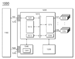
도 11은 본 발명의 실시 예에 따른 SSD를 포함하는 데이터 처리 시스템을 예시적으로 보여주는 도면이다. 도 11을 참조하면, 데이터 처리 시스템(1000)은 호스트 장치(1100)와 SSD(1200) 를 포함할 수 있다.11 is a diagram exemplarily showing a data processing system including an SSD according to an embodiment of the present invention. Referring to FIG. 11, the
SSD(1200)는 컨트롤러(1210), 버퍼 메모리 장치(1220), 비휘발성 메모리 장치들(1231~123n), 전원 공급기(1240), 신호 커넥터(1250) 및 전원 커넥터(1260)를 포함할 수 있다.The
컨트롤러(1210)는 SSD(1200)의 제반 동작을 제어할 수 있다. 컨트롤러(1210)는 호스트 인터페이스 유닛(1211), 컨트롤 유닛(1212), 랜덤 액세스 메모리(1213), 에러 정정 코드(ECC) 유닛(1214) 및 메모리 인터페이스 유닛(1215)을 포함할 수 있다.The
호스트 인터페이스 유닛(1211)은 신호 커넥터(1250)를 통해서 호스트 장치(1100)와 신호(SGL)를 주고 받을 수 있다. 여기에서, 신호(SGL)는 커맨드, 어드레스, 데이터 등을 포함할 수 있다. 호스트 인터페이스 유닛(1211)은, 호스트 장치(1100)의 프로토콜에 따라서, 호스트 장치(1100)와 SSD(1200)를 인터페이싱할 수 있다. 예를 들면, 호스트 인터페이스 유닛(1211)은, 시큐어 디지털(secure digital), USB(universal serial bus), MMC(multi-media card), eMMC(embedded MMC), PCMCIA(personal computer memory card international association), PATA(parallel advanced technology attachment), SATA(serial advanced technology attachment), SCSI(small computer system interface), SAS(serial attached SCSI), PCI(peripheral component interconnection), PCI-E(PCI Express), UFS(universal flash storage)와 같은 표준 인터페이스 프로토콜들 중 어느 하나를 통해서 호스트 장치(1100)와 통신할 수 있다.The
컨트롤 유닛(1212)은 호스트 장치(1100)로부터 입력된 신호(SGL)를 분석하고 처리할 수 있다. 컨트롤 유닛(1212)은 SSD(1200)를 구동하기 위한 펌웨어 또는 소프트웨어에 따라서 내부 기능 블록들의 동작을 제어할 수 있다. 랜덤 액세스 메모리(1213)는 이러한 펌웨어 또는 소프트웨어를 구동하기 위한 동작 메모리로서 사용될 수 있다.The
에러 정정 코드(ECC) 유닛(1214)은 비휘발성 메모리 장치들(1231~123n)로 전송될 데이터의 패리티 데이터를 생성할 수 있다. 생성된 패리티 데이터는 데이터와 함께 비휘발성 메모리 장치들(1231~123n)에 저장될 수 있다. 에러 정정 코드(ECC) 유닛(1214)은 패리티 데이터에 근거하여 비휘발성 메모리 장치들(1231~123n)로부터 독출된 데이터의 에러를 검출할 수 있다. 만약, 검출된 에러가 정정 범위 내이면, 에러 정정 코드(ECC) 유닛(1214)은 검출된 에러를 정정할 수 있다.The error correction code (ECC)
메모리 인터페이스 유닛(1215)은, 컨트롤 유닛(1212)의 제어에 따라서, 비휘발성 메모리 장치들(1231~123n)에 커맨드 및 어드레스와 같은 제어 신호를 제공할 수 있다. 그리고 메모리 인터페이스 유닛(1215)은, 컨트롤 유닛(1212)의 제어에 따라서, 비휘발성 메모리 장치들(1231~123n)과 데이터를 주고받을 수 있다. 예를 들면, 메모리 인터페이스 유닛(1215)은 버퍼 메모리 장치(1220)에 저장된 데이터를 비휘발성 메모리 장치들(1231~123n)로 제공하거나, 비휘발성 메모리 장치들(1231~123n)로부터 읽혀진 데이터를 버퍼 메모리 장치(1220)로 제공할 수 있다.The
버퍼 메모리 장치(1220)는 비휘발성 메모리 장치들(1231~123n)에 저장될 데이터를 임시 저장할 수 있다. 또한, 버퍼 메모리 장치(1220)는 비휘발성 메모리 장치들(1231~123n)로부터 읽혀진 데이터를 임시 저장할 수 있다. 버퍼 메모리 장치(1220)에 임시 저장된 데이터는 컨트롤러(1210)의 제어에 따라 호스트 장치(1100) 또는 비휘발성 메모리 장치들(1231~123n)로 전송될 수 있다.The
비휘발성 메모리 장치들(1231~123n)은 SSD(1200)의 저장 매체로 사용될 수 있다. 비휘발성 메모리 장치들(1231~123n) 각각은 복수의 채널들(CH1~CHn)을 통해 컨트롤러(1210)와 연결될 수 있다. 하나의 채널에는 하나 또는 그 이상의 비휘발성 메모리 장치가 연결될 수 있다. 하나의 채널에 연결되는 비휘발성 메모리 장치들은 동일한 신호 버스 및 데이터 버스에 연결될 수 있다.The
전원 공급기(1240)는 전원 커넥터(1260)를 통해 입력된 전원(PWR)을 SSD(1200) 내부에 제공할 수 있다. 전원 공급기(1240)는 보조 전원 공급기(1241)를 포함할 수 있다. 보조 전원 공급기(1241)는 서든 파워 오프(sudden power off)가 발생되는 경우, SSD(1200)가 정상적으로 종료될 수 있도록 전원을 공급할 수 있다. 보조 전원 공급기(1241)는 대용량 캐패시터들(capacitors)을 포함할 수 있다.The
신호 커넥터(1250)는 호스트 장치(1100)와 SSD(1200)의 인터페이스 방식에 따라서 다양한 형태의 커넥터로 구성될 수 있다.The
전원 커넥터(1260)는 호스트 장치(1100)의 전원 공급 방식에 따라서 다양한 형태의 커넥터로 구성될 수 있다.The
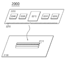
도 12는 본 발명의 실시 예에 따른 메모리 시스템을 포함하는 데이터 처리 시스템을 예시적으로 보여주는 도면이다. 도 12를 참조하면, 데이터 처리 시스템(2000)은 호스트 장치(2100)와 메모리 시스템(2200)을 포함할 수 있다.12 is a diagram exemplarily showing a data processing system including a memory system according to an embodiment of the present invention. Referring to FIG. 12, the
호스트 장치(2100)는 인쇄 회로 기판(printed circuit board)과 같은 기판(board) 형태로 구성될 수 있다. 비록 도시되지 않았지만, 호스트 장치(2100)는 호스트 장치의 기능을 수행하기 위한 내부 기능 블록들을 포함할 수 있다.The
호스트 장치(2100)는 소켓(socket), 슬롯(slot) 또는 커넥터(connector)와 같은 접속 터미널(2110)을 포함할 수 있다. 메모리 시스템(2200)은 접속 터미널(2110)에 마운트(mount)될 수 있다.The
메모리 시스템(2200)은 인쇄 회로 기판과 같은 기판 형태로 구성될 수 있다. 메모리 시스템(2200)은 메모리 모듈 또는 메모리 카드로 불릴 수 있다. 메모리 시스템(2200)은 컨트롤러(2210), 버퍼 메모리 장치(2220), 비휘발성 메모리 장치(2231~2232), PMIC(power management integrated circuit)(2240) 및 접속 터미널(2250)을 포함할 수 있다.The
컨트롤러(2210)는 메모리 시스템(2200)의 제반 동작을 제어할 수 있다. 컨트롤러(2210)는 도 11에 도시된 컨트롤러(1210)와 동일하게 구성될 수 있다.The
버퍼 메모리 장치(2220)는 비휘발성 메모리 장치들(2231~2232)에 저장될 데이터를 임시 저장할 수 있다. 또한, 버퍼 메모리 장치(2220)는 비휘발성 메모리 장치들(2231~2232)로부터 읽혀진 데이터를 임시 저장할 수 있다. 버퍼 메모리 장치(2220)에 임시 저장된 데이터는 컨트롤러(2210)의 제어에 따라 호스트 장치(2100) 또는 비휘발성 메모리 장치들(2231~2232)로 전송될 수 있다.The
비휘발성 메모리 장치들(2231~2232)은 메모리 시스템(2200)의 저장 매체로 사용될 수 있다.The nonvolatile memory devices 2231-2232 may be used as a storage medium of the
PMIC(2240)는 접속 터미널(2250)을 통해 입력된 전원을 메모리 시스템(2200) 내부에 제공할 수 있다. PMIC(2240)는, 컨트롤러(2210)의 제어에 따라서, 메모리 시스템(2200)의 전원을 관리할 수 있다.The
접속 터미널(2250)은 호스트 장치의 접속 터미널(2110)에 연결될 수 있다. 접속 터미널(2250)을 통해서, 호스트 장치(2100)와 메모리 시스템(2200) 간에 커맨드, 어드레스, 데이터 등과 같은 신호와, 전원이 전달될 수 있다. 접속 터미널(2250)은 호스트 장치(2100)와 메모리 시스템(2200)의 인터페이스 방식에 따라 다양한 형태로 구성될 수 있다. 접속 터미널(2250)은 메모리 시스템(2200)의 어느 한 변에 배치될 수 있다.The
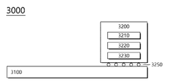
도 13은 본 발명의 실시 예에 따른 메모리 시스템을 포함하는 데이터 처리 시스템을 예시적으로 보여주는 도면이다. 도 13을 참조하면, 데이터 처리 시스템(2000)은 호스트 장치(2100)와 메모리 시스템(2200)을 포함할 수 있다.13 is a diagram exemplarily showing a data processing system including a memory system according to an embodiment of the present invention. Referring to FIG. 13, the
호스트 장치(2100)는 인쇄 회로 기판(printed circuit board)과 같은 기판(board) 형태로 구성될 수 있다. 비록 도시되지 않았지만, 호스트 장치(2100)는 호스트 장치의 기능을 수행하기 위한 내부 기능 블록들을 포함할 수 있다.The
메모리 시스템(2200)은 표면 실장형 패키지 형태로 구성될 수 있다. 메모리 시스템(2200)은 솔더 볼(solder ball)(3250)을 통해서 호스트 장치(2100)에 마운트될 수 있다. 메모리 시스템(2200)은 컨트롤러(3210), 버퍼 메모리 장치(3220) 및 비휘발성 메모리 장치(3230)를 포함할 수 있다.The
컨트롤러(3210)는 메모리 시스템(2200)의 제반 동작을 제어할 수 있다. 컨트롤러(3210)는 도 11에 도시된 컨트롤러(1210)와 동일하게 구성될 수 있다.The
버퍼 메모리 장치(3220)는 비휘발성 메모리 장치(3230)에 저장될 데이터를 임시 저장할 수 있다. 또한, 버퍼 메모리 장치(3220)는 비휘발성 메모리 장치들(3230)로부터 읽혀진 데이터를 임시 저장할 수 있다. 버퍼 메모리 장치(3220)에 임시 저장된 데이터는 컨트롤러(3210)의 제어에 따라 호스트 장치(2100) 또는 비휘발성 메모리 장치(3230)로 전송될 수 있다.The
비휘발성 메모리 장치(3230)는 메모리 시스템(2200)의 저장 매체로 사용될 수 있다.The
도 14는 본 발명의 실시 예에 따른 메모리 시스템을 포함하는 네트워크 시스템을 예시적으로 보여주는 도면이다. 도 14를 참조하면, 네트워크 시스템(4000)은 네트워크(4500)를 통해서 연결된 서버 시스템(4200) 및 복수의 클라이언트 시스템들(4410~4430)을 포함할 수 있다.14 is a diagram exemplarily showing a network system including a memory system according to an embodiment of the present invention. Referring to FIG. 14, the
서버 시스템(4200)은 복수의 클라이언트 시스템들(4410~4430)의 요청에 응답하여 데이터를 서비스할 수 있다. 예를 들면, 서버 시스템(4200)은 복수의 클라이언트 시스템들(4410~4430)로부터 제공된 데이터를 저장할 수 있다. 다른 예로서, 서버 시스템(4200)은 복수의 클라이언트 시스템들(4410~4430)로 데이터를 제공할 수 있다.The
서버 시스템(4200)은 호스트 장치(4100) 및 메모리 시스템(4200)을 포함할 수 있다. 메모리 시스템(4200)은 도 1의 메모리 시스템(10), 도 11의 SSD(1200), 도 12의 메모리 시스템(2200), 도 13의 메모리 시스템(2200)로 구성될 수 있다.The
도 15는 본 발명의 실시 예에 따른 메모리 시스템에 포함된 비휘발성 메모리 장치를 예시적으로 보여주는 블록도이다. 도 15를 참조하면, 비휘발성 메모리 장치는 메모리 셀 어레이(210), 행 디코더(220), 데이터 읽기/쓰기 블록(230), 열 디코더(240), 전압 발생기(250) 및 제어 로직(260)을 포함할 수 있다.15 is a block diagram exemplarily showing a nonvolatile memory device included in a memory system according to an embodiment of the present invention. 15, the nonvolatile memory device includes a
메모리 셀 어레이(210)는 워드 라인들(WL1~WLm)과 비트 라인들(BL1~BLn)이 서로 교차된 영역에 배열된 메모리 셀(MC)들을 포함할 수 있다.The
행 디코더(220)는 워드 라인들(WL1~WLm)을 통해서 메모리 셀 어레이(210)와 연결될 수 있다. 행 디코더(220)는 제어 로직(260)의 제어에 따라 동작할 수 있다. 행 디코더(220)는 외부 장치(도시되지 않음)로부터 제공된 어드레스를 디코딩할 수 있다. 행 디코더(220)는 디코딩 결과에 근거하여 워드 라인들(WL1~WLm)을 선택하고, 구동할 수 있다. 예시적으로, 행 디코더(220)는 전압 발생기(250)로부터 제공된 워드 라인 전압을 워드 라인들(WL1~WLm)에 제공할 수 있다.The
데이터 읽기/쓰기 블록(230)은 비트 라인들(BL1~BLn)을 통해서 메모리 셀 어레이(210)와 연결될 수 있다. 데이터 읽기/쓰기 블록(230)은 비트 라인들(BL1~BLn) 각각에 대응하는 읽기/쓰기 회로들(RW1~RWn)을 포함할 수 있다. 데이터 읽기/쓰기 블록(230)은 제어 로직(260)의 제어에 따라 동작할 수 있다. 데이터 읽기/쓰기 블록(230)은 동작 모드에 따라서 쓰기 드라이버로서 또는 감지 증폭기로서 동작할 수 있다. 예를 들면, 데이터 읽기/쓰기 블록(230)은 쓰기 동작 시 외부 장치로부터 제공된 데이터를 메모리 셀 어레이(210)에 저장하는 쓰기 드라이버로서 동작할 수 있다. 다른 예로서, 데이터 읽기/쓰기 블록(230)은 읽기 동작 시 메모리 셀 어레이(210)로부터 데이터를 독출하는 감지 증폭기로서 동작할 수 있다.The data read /
열 디코더(240)는 제어 로직(260)의 제어에 따라 동작할 수 있다. 열 디코더(240)는 외부 장치로부터 제공된 어드레스를 디코딩할 수 있다. 열 디코더(240)는 디코딩 결과에 근거하여 비트 라인들(BL1~BLn) 각각에 대응하는 데이터 읽기/쓰기 블록(230)의 읽기/쓰기 회로들(RW1~RWn)과 데이터 입출력 라인(또는 데이터 입출력 버퍼)을 연결할 수 있다.The
전압 발생기(250)는 비휘발성 메모리 장치의 내부 동작에 사용되는 전압을 생성할 수 있다. 전압 발생기(250)에 의해서 생성된 전압들은 메모리 셀 어레이(210)의 메모리 셀들에 인가될 수 있다. 예를 들면, 프로그램 동작 시 생성된 프로그램 전압은 프로그램 동작이 수행될 메모리 셀들의 워드 라인에 인가될 수 있다. 다른 예로서, 소거 동작 시 생성된 소거 전압은 소거 동작이 수행될 메모리 셀들의 웰-영역에 인가될 수 있다. 다른 예로서, 읽기 동작 시 생성된 읽기 전압은 읽기 동작이 수행될 메모리 셀들의 워드 라인에 인가될 수 있다.The
제어 로직(260)은 외부 장치로부터 제공된 제어 신호에 근거하여 비휘발성 메모리 장치의 제반 동작을 제어할 수 있다. 예를 들면, 제어 로직(260)은 비휘발성 메모리 장치의 읽기, 쓰기, 소거 동작을 제어할 수 있다.The
본 발명의 일 실시 예에 따른 방법과 관련하여서는 전술한 시스템에 대한 내용이 적용될 수 있다. 따라서, 방법과 관련하여, 전술한 시스템에 대한 내용과 동일한 내용에 대하여는 설명을 생략하였다.With respect to the method according to an embodiment of the present invention, the contents of the above-described system may be applied. Therefore, with respect to the method, descriptions of contents identical to those of the above-described system are omitted.
이상에서, 본 발명은 구체적인 실시 예를 통해 설명되고 있으나, 본 발명은 그 범위에서 벗어나지 않는 한도 내에서 여러 가지로 변형할 수 있음은 잘 이해될 것이다. 그러므로, 본 발명의 범위는 상술한 실시 예에 국한되어 정해져서는 안되며, 후술하는 특허청구범위 및 이와 균등한 것들에 의해 정해져야 한다. 본 발명의 범위 또는 기술적 사상을 벗어나지 않고 본 발명의 구조가 다양하게 수정되거나 변경될 수 있음은 잘 이해될 것이다.In the above, the present invention has been described through specific examples, but it will be understood that the present invention can be modified in various ways without departing from its scope. Therefore, the scope of the present invention should not be determined by being limited to the above-described embodiments, but should be defined by the following claims and equivalents thereto. It will be understood that the structure of the present invention may be variously modified or changed without departing from the scope or technical spirit of the present invention.
10 : 메모리 시스템
20 : 호스트 장치
100 : 컨트롤러
110 : 컨트롤 유닛
120 : 랜덤 액세스 메모리
200 : 비휘발성 메모리 장치10: memory system
20: host device
100: controller
110: control unit
120: random access memory
200: non-volatile memory device
Claims (20)
희생(victim) 블록을 선택하는 단계;
빈 블록들 중에서 복수의 타겟 블록들을 선택하는 단계;
상기 타겟 블록들 각각에 상기 논리 어드레스 그룹들 중 적어도 하나의 논리 어드레스 그룹을 맵핑하는 단계;
상기 논리 어드레스 그룹들 중에서, 상기 희생 블록에 저장된 제1 유효 데이터의 논리 어드레스를 포함하는 제1 논리 어드레스 그룹을 판단하는 단계;
상기 제1 유효 데이터를 상기 타겟 블록들 중에서 상기 제1 논리 어드레스 그룹에 맵핑된 제1 타겟 블록에 백업하는 단계를 포함하는, 방법.A method of operating a memory system to which a plurality of logical address groups, each having a predetermined logical address range, is applied,
Selecting a victim block;
Selecting a plurality of target blocks from among the empty blocks;
Mapping at least one logical address group of the logical address groups to each of the target blocks;
Determining, among the logical address groups, a first logical address group including a logical address of first valid data stored in the victim block;
And backing up the first valid data to a first target block mapped to the first logical address group among the target blocks.
상기 타겟 블록들 각각에 상기 적어도 하나의 논리 어드레스 그룹을 맵핑하는 단계는,
상기 논리 어드레스 그룹들 중, 상기 희생 블록에 저장된 유효 데이터의 논리 어드레스들을 가장 많이 포함하는 논리 어드레스 그룹을 결정하는 단계;
상기 타겟 블록들 중 어느 하나의 타겟 블록에 상기 결정된 논리 어드레스 그룹을 맵핑하는 단계; 및
상기 타겟 블록들 중 다른 하나의 타겟 블록에 상기 논리 어드레스 그룹들 중 상기 결정된 논리 어드레스 그룹을 제외한 나머지 논리 어드레스 그룹들을 맵핑하는 단계를 포함하는, 방법According to claim 1,
Mapping the at least one logical address group to each of the target blocks,
Determining, among the logical address groups, a logical address group that includes the most logical addresses of valid data stored in the victim block;
Mapping the determined logical address group to any one of the target blocks; And
And mapping the logical address groups other than the determined logical address group among the logical address groups to another target block of the target blocks.
상기 타겟 블록들 각각에 상기 적어도 하나의 논리 어드레스 그룹을 맵핑하는 단계는,
상기 논리 어드레스 그룹들이 가지는 오프셋 값들에 따라, 상기 타겟 블록들 각각에 상기 적어도 하나의 논리 어드레스 그룹을 맵핑하는 단계를 포함하는, 방법.According to claim 1,
Mapping the at least one logical address group to each of the target blocks,
And mapping the at least one logical address group to each of the target blocks according to the offset values of the logical address groups.
상기 희생 블록에 대한 맵핑 정보가 저장된 맵핑 테이블에 근거하여 상기 제1 유효 데이터를 선별하는 단계를 더 포함하는, 방법.According to claim 1,
And selecting the first valid data based on a mapping table in which mapping information for the victim block is stored.
상기 맵핑 테이블은, 상기 희생 블록에서 상기 제1 유효 데이터가 저장된 위치에 관한 물리 어드레스와 상기 제1 유효 데이터의 상기 논리 어드레스 사이의 맵핑 정보를 포함하는, 방법.According to claim 4,
And the mapping table includes mapping information between a physical address of a location where the first valid data is stored in the victim block and the logical address of the first valid data.
상기 희생 블록 및 상기 타겟 블록들 각각은, 상기 메모리 시스템에 포함된 복수의 비휘발성 메모리 장치들에 각각 포함된 복수의 메모리 블록들을 포함하는 슈퍼 블록 단위로 설정되는, 방법.According to claim 1,
Each of the sacrificial block and the target blocks is set in units of super blocks including a plurality of memory blocks respectively included in a plurality of nonvolatile memory devices included in the memory system.
희생 블록을 선택하는 단계;
빈 블록들 중에서 상기 희생 블록에 저장된 유효 데이터가 백업되는 타겟 블록을 선택하는 단계;
상기 논리 어드레스 그룹들의 백업 순서를 결정하되, 상기 백업 순서는 상기 각각의 논리 어드레스 그룹들에 대응하는 유효 데이터가 상기 타겟 블록에 백업되는 순서인, 결정하는 단계; 및
상기 백업 순서에 기초하여 상기 유효 데이터 중 선택된 유효 데이터를 상기 타겟 블록으로 백업하는 단계를 포함하는, 방법.A method of operating a memory system to which a plurality of logical address groups, each having a predetermined logical address range, is applied,
Selecting a sacrificial block;
Selecting a target block from which valid data stored in the victim block is backed up among empty blocks;
Determining a backup order of the logical address groups, wherein the backup order is an order in which valid data corresponding to the respective logical address groups are backed up to the target block; And
And backing up selected valid data among the valid data to the target block based on the backup order.
상기 백업 순서를 결정하는 단계는,
상기 타겟 블록을 구성하는 복수의 영역들 중 유효 데이터가 가장 먼저 백업될 제1 영역을 선택하는 단계;
상기 논리 어드레스 그룹들 중 상기 제1 영역에 맵핑될 제1 논리 어드레스 그룹을 선택하는 단계를 포함하는, 방법.The method of claim 7,
Determining the order of the backup,
Selecting a first region from which valid data is to be first backed up among a plurality of regions constituting the target block;
And selecting a first logical address group to be mapped to the first area among the logical address groups.
상기 선택된 유효 데이터를 상기 타겟 블록으로 백업하는 단계는,
상기 제1 영역에 상기 제1 논리 어드레스 그룹에 대응하는 유효 데이터를 백업하는 단계; 및
상기 복수의 영역들 중 제2 영역에 상기 논리 어드레스 그룹들 중 상기 제1 논리 어드레스 그룹 이외의 논리 어드레스 그룹들에 대응하는 유효 데이터를 백업하는 단계를 포함하는, 방법.The method of claim 8,
The step of backing up the selected valid data to the target block,
Backing up valid data corresponding to the first logical address group to the first area; And
And backing up valid data corresponding to logical address groups other than the first logical address group of the logical address groups to a second one of the plurality of areas.
상기 제1 영역은 제1 칩 인에이블 신호에 의하여 구동되고,
상기 제2 영역은 제2 칩 인에이블 신호에 의하여 구동되고,
상기 제1 칩 인에이블 신호는, 상기 타겟 블록을 구동하는 칩 인에이블 신호들 중 가장 먼저 생성되는 칩 인에이블 신호인, 방법.The method of claim 9,
The first region is driven by a first chip enable signal,
The second region is driven by a second chip enable signal,
The first chip enable signal is a chip enable signal generated first among chip enable signals driving the target block.
상기 제1 논리 어드레스 그룹을 선택하는 단계는,
상기 논리 어드레스 그룹들 중, 상기 희생 블록에 저장된 상기 유효 데이터에 대응하는 논리 어드레스들을 가장 많이 포함하는 논리 어드레스 그룹을 상기 제1 논리 어드레스 그룹으로 선택하는 단계를 포함하는, 방법.The method of claim 8,
The step of selecting the first logical address group may include:
And selecting, among the logical address groups, the logical address group including the most logical addresses corresponding to the valid data stored in the victim block as the first logical address group.
상기 제1 논리 어드레스 그룹을 선택하는 단계는,
상기 논리 어드레스 그룹들이 서로 다른 오프셋 값들을 가질 때, 상기 논리 어드레스 그룹들 중 기설정된 오프셋 값을 갖는 논리 어드레스 그룹을 상기 제1 논리 어드레스 그룹으로 선택하는 단계를 포함하는, 방법.The method of claim 8,
The step of selecting the first logical address group may include:
And when the logical address groups have different offset values, selecting a logical address group having a preset offset value among the logical address groups as the first logical address group.
상기 희생 블록에 대한 맵핑 정보가 저장된 맵핑 테이블에 근거하여 상기 유효 데이터를 선별하는 단계를 더 포함하는, 방법.The method of claim 7,
And selecting the valid data based on a mapping table in which mapping information for the victim block is stored.
상기 맵핑 테이블은, 상기 희생 블록에서 상기 유효 데이터가 저장된 위치에 관한 물리 어드레스와 상기 유효 데이터의 논리 어드레스 사이의 맵핑 정보를 포함하는, 방법.The method of claim 13,
The mapping table includes mapping information between a physical address of a location where the valid data is stored in the victim block and a logical address of the valid data.
상기 희생 블록 및 상기 타겟 블록 각각은, 상기 메모리 시스템에 포함된 복수의 비휘발성 메모리 장치들에 각각 포함된 복수의 메모리 블록들을 포함하는 슈퍼 블록 단위로 설정되는, 방법.The method of claim 7,
Each of the sacrificial block and the target block is set in units of super blocks including a plurality of memory blocks respectively included in a plurality of nonvolatile memory devices included in the memory system.
복수의 메모리 블록들을 포함하는 비휘발성 메모리 장치들; 및
상기 메모리 블록들을 상기 비휘발성 메모리 장치들에 걸쳐 복수의 슈퍼 블록들로 그룹핑하고, 상기 슈퍼 블록들 중에서 희생(victim) 블록을 선택하고, 상기 희생 블록에 대한 내부 백업 동작을 제어하도록 구성된 컨트롤러를 포함하되,
상기 컨트롤러는,
상기 논리 어드레스 그룹들 중 상기 희생 블록에 저장된 유효 데이터의 논리 어드레스들을 포함하는 논리 어드레스 그룹들을 판단하고, 상기 판단된 논리 어드레스 그룹들에 맵핑된 위치들에 상기 유효 데이터를 백업하는, 메모리 시스템.In a memory system to which a plurality of logical address groups, each having a predetermined logical address range, is applied,
Non-volatile memory devices including a plurality of memory blocks; And
And a controller configured to group the memory blocks into a plurality of super blocks across the non-volatile memory devices, select a victim block among the super blocks, and control an internal backup operation for the victim block. Ha,
The controller,
And determining logical address groups including logical addresses of valid data stored in the victim block among the logical address groups, and backing up the valid data to locations mapped to the determined logical address groups.
상기 컨트롤러는,
빈 슈퍼 블록들 중에서 복수의 타겟 블록들을 선택하고,
상기 타겟 블록들 각각에 상기 논리 어드레스 그룹들 중 적어도 하나의 논리 어드레스 그룹을 맵핑하고,
상기 논리 어드레스 그룹들 중에서, 상기 희생 블록에 저장된 제1 유효 데이터의 논리 어드레스를 포함하는 제1 논리 어드레스 그룹을 판단하고,
상기 제1 유효 데이터를 상기 타겟 블록들 중에서 상기 제1 논리 어드레스 그룹에 맵핑된 제1 타겟 블록에 백업하는, 메모리 시스템.The method of claim 16,
The controller,
Select a plurality of target blocks from the empty super blocks,
Mapping at least one logical address group among the logical address groups to each of the target blocks,
Among the logical address groups, a first logical address group including a logical address of the first valid data stored in the victim block is determined,
And backing up the first valid data to a first target block mapped to the first logical address group among the target blocks.
상기 컨트롤러는,
상기 논리 어드레스 그룹들 중, 상기 희생 블록에 저장된 유효 데이터의 논리 어드레스들을 가장 많이 포함하는 논리 어드레스 그룹을 결정하고,
상기 타겟 블록들 중 어느 하나의 타겟 블록에 상기 결정된 논리 어드레스 그룹을 맵핑하고,
상기 타겟 블록들 중 다른 하나의 타겟 블록에 상기 논리 어드레스 그룹들 중 상기 결정된 논리 어드레스 그룹을 제외한 나머지 논리 어드레스 그룹들을 맵핑하는, 메모리 시스템.The method of claim 17,
The controller,
Among the logical address groups, a logical address group that includes the most logical addresses of valid data stored in the victim block is determined,
Mapping the determined logical address group to any one of the target blocks,
And map the remaining logical address groups of the logical address groups excluding the determined logical address group among the logical address groups to another target block of the target blocks.
상기 컨트롤러는,
빈 슈퍼 블록들 중에서 타겟 블록을 선택하고,
상기 타겟 블록에 포함된 복수의 영역들 각각에 상기 논리 어드레스 그룹들 중 적어도 하나의 논리 어드레스 그룹을 맵핑하되, 상기 영역들은 서로 다른 칩 인에이블 신호들에 의하여 각각 구동되고,
상기 논리 어드레스 그룹들 중에서, 상기 희생 블록에 저장된 제1 유효 데이터의 논리 어드레스를 포함하는 제1 논리 어드레스 그룹을 판단하고,
상기 제1 유효 데이터를 상기 영역들 중에서 상기 제1 논리 어드레스 그룹에 맵핑된 제1 영역에 백업하는, 메모리 시스템.The method of claim 16,
The controller,
Select a target block from among empty super blocks,
Mapping at least one logical address group among the logical address groups to each of the plurality of regions included in the target block, wherein the regions are respectively driven by different chip enable signals,
Among the logical address groups, a first logical address group including a logical address of the first valid data stored in the victim block is determined,
A memory system for backing up the first valid data to a first area mapped to the first logical address group among the areas.
상기 컨트롤러는,
상기 제1 영역에 상기 제1 논리 어드레스 그룹을 맵핑하고, 상기 영역들 중 제2 영역에 상기 제1 논리 어드레스 그룹을 제외한 나머지 논리 어드레스 그룹들을 맵핑하고,
상기 제1 논리 어드레스 그룹은,
상기 논리 어드레스 그룹들 중, 상기 희생 블록에 저장된 유효 데이터의 논리 어드레스들을 가장 많이 포함하는 논리 어드레스 그룹이고,
상기 제1 영역은,
상기 칩 인에이블 신호들 중 가장 먼저 생성되는 칩 인에이블 신호에 의해 구동되는, 메모리 시스템.The method of claim 19,
The controller,
The first logical address group is mapped to the first region, and the remaining logical address groups other than the first logical address group are mapped to a second region of the regions,
The first logical address group,
Among the logical address groups, the logical address group includes the most logical addresses of valid data stored in the victim block,
The first region,
A memory system driven by a chip enable signal generated first among the chip enable signals.
Priority Applications (3)
| Application Number | Priority Date | Filing Date | Title |
|---|---|---|---|
| KR1020180111661A KR102585883B1 (en) | 2018-09-18 | 2018-09-18 | Operating method of memory system and memory system |
| US16/224,955 US11086772B2 (en) | 2018-09-18 | 2018-12-19 | Memory system performing garbage collection operation and operating method of memory system |
| CN201811636994.0A CN110908594B (en) | 2018-09-18 | 2018-12-29 | Memory system and operation method thereof |
Applications Claiming Priority (1)
| Application Number | Priority Date | Filing Date | Title |
|---|---|---|---|
| KR1020180111661A KR102585883B1 (en) | 2018-09-18 | 2018-09-18 | Operating method of memory system and memory system |
Publications (2)
| Publication Number | Publication Date |
|---|---|
| KR20200032527A true KR20200032527A (en) | 2020-03-26 |
| KR102585883B1 KR102585883B1 (en) | 2023-10-10 |
Family
ID=69774065
Family Applications (1)
| Application Number | Title | Priority Date | Filing Date |
|---|---|---|---|
| KR1020180111661A KR102585883B1 (en) | 2018-09-18 | 2018-09-18 | Operating method of memory system and memory system |
Country Status (3)
| Country | Link |
|---|---|
| US (1) | US11086772B2 (en) |
| KR (1) | KR102585883B1 (en) |
| CN (1) | CN110908594B (en) |
Families Citing this family (7)
| Publication number | Priority date | Publication date | Assignee | Title |
|---|---|---|---|---|
| TWI718492B (en) * | 2019-03-12 | 2021-02-11 | 群聯電子股份有限公司 | Data storing method, memory storage apparatus and memory control circuit unit |
| KR20200110859A (en) * | 2019-03-18 | 2020-09-28 | 에스케이하이닉스 주식회사 | Data Storage Apparatus, Computing Device Having the Same and Operation Method Thereof |
| KR20210012329A (en) * | 2019-07-24 | 2021-02-03 | 에스케이하이닉스 주식회사 | Memory system and operating method of the memory system |
| KR20220028332A (en) * | 2020-08-28 | 2022-03-08 | 에스케이하이닉스 주식회사 | Storage device and operating method thereof |
| US20220222008A1 (en) * | 2021-01-14 | 2022-07-14 | Silicon Motion, Inc. | Method for managing flash memory module and associated flash memory controller and memory device |
| TWI766582B (en) * | 2021-02-17 | 2022-06-01 | 群聯電子股份有限公司 | Valid data merging method, memory storage device and memory control circuit unit |
| CN115495287B (en) * | 2022-11-16 | 2024-04-09 | 珠海妙存科技有限公司 | Data backup method and device for MLC NAND and electronic equipment |
Citations (4)
| Publication number | Priority date | Publication date | Assignee | Title |
|---|---|---|---|---|
| KR20100078450A (en) * | 2008-12-30 | 2010-07-08 | 아주대학교산학협력단 | Flash memory device and memory management method therein |
| JP2015001908A (en) * | 2013-06-17 | 2015-01-05 | 富士通株式会社 | Information processing device, control circuit, control program, and control method |
| US20170286286A1 (en) * | 2016-03-29 | 2017-10-05 | Micron Technology, Inc. | Memory devices including dynamic superblocks, and related methods and electronic systems |
| KR20180064542A (en) * | 2015-10-30 | 2018-06-14 | 마이크론 테크놀로지, 인크. | Data transfer techniques for multiple devices on a shared bus |
Family Cites Families (12)
| Publication number | Priority date | Publication date | Assignee | Title |
|---|---|---|---|---|
| CN101176074B (en) * | 2005-12-09 | 2010-12-15 | 松下电器产业株式会社 | Nonvolatile memory device, method of writing data, and method of reading out data |
| CN101169762A (en) * | 2006-10-27 | 2008-04-30 | 北京中电华大电子设计有限责任公司 | Software and hard disk cooperated protection mechanism facing to intelligent card |
| US8166233B2 (en) * | 2009-07-24 | 2012-04-24 | Lsi Corporation | Garbage collection for solid state disks |
| US8463826B2 (en) * | 2009-09-03 | 2013-06-11 | Apple Inc. | Incremental garbage collection for non-volatile memories |
| CN102081576B (en) * | 2011-03-01 | 2012-07-11 | 华中科技大学 | Flash memory wear balance method |
| CN103150261B (en) * | 2013-03-11 | 2017-02-08 | 北京忆恒创源科技有限公司 | Method and device for simultaneously accessing multiple solid-state disks |
| US9753653B2 (en) * | 2015-04-14 | 2017-09-05 | Sandisk Technologies Llc | High-priority NAND operations management |
| KR102509540B1 (en) | 2015-06-30 | 2023-03-14 | 삼성전자주식회사 | Storage device and garbage collection method thereof |
| CN106445740A (en) * | 2016-09-22 | 2017-02-22 | 深圳市先天海量信息技术有限公司 | Control method and control system for NAND flash memory data in solid state disk |
| JP2018181213A (en) * | 2017-04-20 | 2018-11-15 | 富士通株式会社 | Device, method, and program for storage control |
| JP2018181207A (en) * | 2017-04-20 | 2018-11-15 | 富士通株式会社 | Device, method, and program for storage control |
| US10452536B2 (en) * | 2017-06-12 | 2019-10-22 | Western Digital Technologies, Inc. | Dynamic management of garbage collection and overprovisioning for host stream storage |
-
2018
- 2018-09-18 KR KR1020180111661A patent/KR102585883B1/en active IP Right Grant
- 2018-12-19 US US16/224,955 patent/US11086772B2/en active Active
- 2018-12-29 CN CN201811636994.0A patent/CN110908594B/en active Active
Patent Citations (4)
| Publication number | Priority date | Publication date | Assignee | Title |
|---|---|---|---|---|
| KR20100078450A (en) * | 2008-12-30 | 2010-07-08 | 아주대학교산학협력단 | Flash memory device and memory management method therein |
| JP2015001908A (en) * | 2013-06-17 | 2015-01-05 | 富士通株式会社 | Information processing device, control circuit, control program, and control method |
| KR20180064542A (en) * | 2015-10-30 | 2018-06-14 | 마이크론 테크놀로지, 인크. | Data transfer techniques for multiple devices on a shared bus |
| US20170286286A1 (en) * | 2016-03-29 | 2017-10-05 | Micron Technology, Inc. | Memory devices including dynamic superblocks, and related methods and electronic systems |
Also Published As
| Publication number | Publication date |
|---|---|
| CN110908594A (en) | 2020-03-24 |
| CN110908594B (en) | 2023-08-25 |
| US20200089603A1 (en) | 2020-03-19 |
| US11086772B2 (en) | 2021-08-10 |
| KR102585883B1 (en) | 2023-10-10 |
Similar Documents
| Publication | Publication Date | Title |
|---|---|---|
| KR102585883B1 (en) | Operating method of memory system and memory system | |
| US9208079B2 (en) | Solid state memory (SSM), computer system including an SSM, and method of operating an SSM | |
| CN107168886B (en) | Data storage device and operation method thereof | |
| US10802733B2 (en) | Methods and apparatus for configuring storage tiers within SSDs | |
| KR102233400B1 (en) | Data storage device and operating method thereof | |
| US10235069B2 (en) | Load balancing by dynamically transferring memory range assignments | |
| US20190317892A1 (en) | Memory system, data processing system, and operating method of memory system | |
| KR102544162B1 (en) | Data storage device and operating method thereof | |
| KR20200114212A (en) | Data storage device and operating method thereof | |
| KR20210144249A (en) | Storage device and operating method of the same | |
| US20220229775A1 (en) | Data storage device and operating method thereof | |
| US11249917B2 (en) | Data storage device and operating method thereof | |
| US20200241955A1 (en) | Data storage device and operating method thereof | |
| US20230126685A1 (en) | Storage device and electronic system | |
| US20190278703A1 (en) | Memory system, operating method thereof and electronic device | |
| CN115458013A (en) | Storage device and operation method thereof | |
| KR20210079894A (en) | Data storage device and operating method thereof | |
| KR20200015185A (en) | Data storage device and operating method thereof | |
| US20220164119A1 (en) | Controller, and memory system and data processing system including the same |
Legal Events
| Date | Code | Title | Description |
|---|---|---|---|
| E902 | Notification of reason for refusal | ||
| E701 | Decision to grant or registration of patent right |