KR20200031048A - Micro-electrical mechanical system sensor package and method of manufacture thereof - Google Patents
Micro-electrical mechanical system sensor package and method of manufacture thereof Download PDFInfo
- Publication number
- KR20200031048A KR20200031048A KR1020190111358A KR20190111358A KR20200031048A KR 20200031048 A KR20200031048 A KR 20200031048A KR 1020190111358 A KR1020190111358 A KR 1020190111358A KR 20190111358 A KR20190111358 A KR 20190111358A KR 20200031048 A KR20200031048 A KR 20200031048A
- Authority
- KR
- South Korea
- Prior art keywords
- mems microphone
- sidewall
- cover
- package
- trace
- Prior art date
Links
- 238000000034 method Methods 0.000 title claims description 39
- 238000004519 manufacturing process Methods 0.000 title description 19
- 239000000758 substrate Substances 0.000 claims description 84
- 238000000465 moulding Methods 0.000 claims description 28
- 150000001875 compounds Chemical class 0.000 claims description 24
- 230000008569 process Effects 0.000 claims description 10
- 239000004020 conductor Substances 0.000 claims description 8
- 238000004891 communication Methods 0.000 claims description 4
- 238000007747 plating Methods 0.000 claims description 4
- 230000008878 coupling Effects 0.000 claims 2
- 238000010168 coupling process Methods 0.000 claims 2
- 238000005859 coupling reaction Methods 0.000 claims 2
- 239000010410 layer Substances 0.000 description 34
- 229910052751 metal Inorganic materials 0.000 description 17
- 239000002184 metal Substances 0.000 description 17
- 239000000853 adhesive Substances 0.000 description 12
- 230000001070 adhesive effect Effects 0.000 description 12
- 230000008901 benefit Effects 0.000 description 9
- 239000000463 material Substances 0.000 description 9
- 230000006870 function Effects 0.000 description 5
- 239000000243 solution Substances 0.000 description 4
- RYGMFSIKBFXOCR-UHFFFAOYSA-N Copper Chemical compound [Cu] RYGMFSIKBFXOCR-UHFFFAOYSA-N 0.000 description 3
- 239000004593 Epoxy Substances 0.000 description 3
- 238000003491 array Methods 0.000 description 3
- 230000015572 biosynthetic process Effects 0.000 description 3
- 229910052802 copper Inorganic materials 0.000 description 3
- 239000010949 copper Substances 0.000 description 3
- 230000007246 mechanism Effects 0.000 description 3
- 238000000429 assembly Methods 0.000 description 2
- 238000005520 cutting process Methods 0.000 description 2
- 230000007423 decrease Effects 0.000 description 2
- 238000005538 encapsulation Methods 0.000 description 2
- 230000004048 modification Effects 0.000 description 2
- 238000012986 modification Methods 0.000 description 2
- 238000007789 sealing Methods 0.000 description 2
- 229910000679 solder Inorganic materials 0.000 description 2
- -1 sub-assemblies Substances 0.000 description 2
- 238000010146 3D printing Methods 0.000 description 1
- XUIMIQQOPSSXEZ-UHFFFAOYSA-N Silicon Chemical compound [Si] XUIMIQQOPSSXEZ-UHFFFAOYSA-N 0.000 description 1
- 239000000956 alloy Substances 0.000 description 1
- 229910045601 alloy Inorganic materials 0.000 description 1
- 229910052782 aluminium Inorganic materials 0.000 description 1
- XAGFODPZIPBFFR-UHFFFAOYSA-N aluminium Chemical compound [Al] XAGFODPZIPBFFR-UHFFFAOYSA-N 0.000 description 1
- 230000000712 assembly Effects 0.000 description 1
- 230000004888 barrier function Effects 0.000 description 1
- 239000000919 ceramic Substances 0.000 description 1
- 230000005465 channeling Effects 0.000 description 1
- 238000003486 chemical etching Methods 0.000 description 1
- 229920001940 conductive polymer Polymers 0.000 description 1
- 230000007613 environmental effect Effects 0.000 description 1
- 238000005530 etching Methods 0.000 description 1
- 239000003292 glue Substances 0.000 description 1
- PCHJSUWPFVWCPO-UHFFFAOYSA-N gold Chemical compound [Au] PCHJSUWPFVWCPO-UHFFFAOYSA-N 0.000 description 1
- 229910052737 gold Inorganic materials 0.000 description 1
- 239000010931 gold Substances 0.000 description 1
- 238000002347 injection Methods 0.000 description 1
- 239000007924 injection Substances 0.000 description 1
- 238000003698 laser cutting Methods 0.000 description 1
- 239000012528 membrane Substances 0.000 description 1
- 239000007769 metal material Substances 0.000 description 1
- 150000002739 metals Chemical class 0.000 description 1
- 238000003801 milling Methods 0.000 description 1
- 238000001020 plasma etching Methods 0.000 description 1
- 235000020004 porter Nutrition 0.000 description 1
- 238000007639 printing Methods 0.000 description 1
- 239000002994 raw material Substances 0.000 description 1
- 230000004044 response Effects 0.000 description 1
- 239000000565 sealant Substances 0.000 description 1
- 102000012498 secondary active transmembrane transporter activity proteins Human genes 0.000 description 1
- 108040003878 secondary active transmembrane transporter activity proteins Proteins 0.000 description 1
- 230000035945 sensitivity Effects 0.000 description 1
- 229910052710 silicon Inorganic materials 0.000 description 1
- 239000010703 silicon Substances 0.000 description 1
- 239000002356 single layer Substances 0.000 description 1
- 239000000126 substance Substances 0.000 description 1
- 230000001629 suppression Effects 0.000 description 1
- 229920001169 thermoplastic Polymers 0.000 description 1
- 239000004416 thermosoftening plastic Substances 0.000 description 1
Images


Classifications
-
- B—PERFORMING OPERATIONS; TRANSPORTING
- B81—MICROSTRUCTURAL TECHNOLOGY
- B81B—MICROSTRUCTURAL DEVICES OR SYSTEMS, e.g. MICROMECHANICAL DEVICES
- B81B7/00—Microstructural systems; Auxiliary parts of microstructural devices or systems
- B81B7/02—Microstructural systems; Auxiliary parts of microstructural devices or systems containing distinct electrical or optical devices of particular relevance for their function, e.g. microelectro-mechanical systems [MEMS]
-
- B—PERFORMING OPERATIONS; TRANSPORTING
- B81—MICROSTRUCTURAL TECHNOLOGY
- B81B—MICROSTRUCTURAL DEVICES OR SYSTEMS, e.g. MICROMECHANICAL DEVICES
- B81B7/00—Microstructural systems; Auxiliary parts of microstructural devices or systems
- B81B7/0032—Packages or encapsulation
- B81B7/0061—Packages or encapsulation suitable for fluid transfer from the MEMS out of the package or vice versa, e.g. transfer of liquid, gas, sound
-
- H—ELECTRICITY
- H04—ELECTRIC COMMUNICATION TECHNIQUE
- H04R—LOUDSPEAKERS, MICROPHONES, GRAMOPHONE PICK-UPS OR LIKE ACOUSTIC ELECTROMECHANICAL TRANSDUCERS; DEAF-AID SETS; PUBLIC ADDRESS SYSTEMS
- H04R19/00—Electrostatic transducers
- H04R19/04—Microphones
-
- B—PERFORMING OPERATIONS; TRANSPORTING
- B81—MICROSTRUCTURAL TECHNOLOGY
- B81B—MICROSTRUCTURAL DEVICES OR SYSTEMS, e.g. MICROMECHANICAL DEVICES
- B81B7/00—Microstructural systems; Auxiliary parts of microstructural devices or systems
- B81B7/0032—Packages or encapsulation
- B81B7/0064—Packages or encapsulation for protecting against electromagnetic or electrostatic interferences
-
- B—PERFORMING OPERATIONS; TRANSPORTING
- B81—MICROSTRUCTURAL TECHNOLOGY
- B81B—MICROSTRUCTURAL DEVICES OR SYSTEMS, e.g. MICROMECHANICAL DEVICES
- B81B7/00—Microstructural systems; Auxiliary parts of microstructural devices or systems
- B81B7/0032—Packages or encapsulation
- B81B7/007—Interconnections between the MEMS and external electrical signals
-
- B—PERFORMING OPERATIONS; TRANSPORTING
- B81—MICROSTRUCTURAL TECHNOLOGY
- B81B—MICROSTRUCTURAL DEVICES OR SYSTEMS, e.g. MICROMECHANICAL DEVICES
- B81B7/00—Microstructural systems; Auxiliary parts of microstructural devices or systems
- B81B7/0032—Packages or encapsulation
- B81B7/0074—3D packaging, i.e. encapsulation containing one or several MEMS devices arranged in planes non-parallel to the mounting board
-
- B—PERFORMING OPERATIONS; TRANSPORTING
- B81—MICROSTRUCTURAL TECHNOLOGY
- B81B—MICROSTRUCTURAL DEVICES OR SYSTEMS, e.g. MICROMECHANICAL DEVICES
- B81B7/00—Microstructural systems; Auxiliary parts of microstructural devices or systems
- B81B7/04—Networks or arrays of similar microstructural devices
-
- B—PERFORMING OPERATIONS; TRANSPORTING
- B81—MICROSTRUCTURAL TECHNOLOGY
- B81C—PROCESSES OR APPARATUS SPECIALLY ADAPTED FOR THE MANUFACTURE OR TREATMENT OF MICROSTRUCTURAL DEVICES OR SYSTEMS
- B81C1/00—Manufacture or treatment of devices or systems in or on a substrate
- B81C1/00015—Manufacture or treatment of devices or systems in or on a substrate for manufacturing microsystems
- B81C1/00214—Processes for the simultaneaous manufacturing of a network or an array of similar microstructural devices
-
- B—PERFORMING OPERATIONS; TRANSPORTING
- B81—MICROSTRUCTURAL TECHNOLOGY
- B81C—PROCESSES OR APPARATUS SPECIALLY ADAPTED FOR THE MANUFACTURE OR TREATMENT OF MICROSTRUCTURAL DEVICES OR SYSTEMS
- B81C1/00—Manufacture or treatment of devices or systems in or on a substrate
- B81C1/00015—Manufacture or treatment of devices or systems in or on a substrate for manufacturing microsystems
- B81C1/00222—Integrating an electronic processing unit with a micromechanical structure
- B81C1/0023—Packaging together an electronic processing unit die and a micromechanical structure die
-
- B—PERFORMING OPERATIONS; TRANSPORTING
- B81—MICROSTRUCTURAL TECHNOLOGY
- B81C—PROCESSES OR APPARATUS SPECIALLY ADAPTED FOR THE MANUFACTURE OR TREATMENT OF MICROSTRUCTURAL DEVICES OR SYSTEMS
- B81C1/00—Manufacture or treatment of devices or systems in or on a substrate
- B81C1/00015—Manufacture or treatment of devices or systems in or on a substrate for manufacturing microsystems
- B81C1/00261—Processes for packaging MEMS devices
- B81C1/00301—Connecting electric signal lines from the MEMS device with external electrical signal lines, e.g. through vias
-
- B—PERFORMING OPERATIONS; TRANSPORTING
- B81—MICROSTRUCTURAL TECHNOLOGY
- B81C—PROCESSES OR APPARATUS SPECIALLY ADAPTED FOR THE MANUFACTURE OR TREATMENT OF MICROSTRUCTURAL DEVICES OR SYSTEMS
- B81C1/00—Manufacture or treatment of devices or systems in or on a substrate
- B81C1/00642—Manufacture or treatment of devices or systems in or on a substrate for improving the physical properties of a device
-
- B—PERFORMING OPERATIONS; TRANSPORTING
- B81—MICROSTRUCTURAL TECHNOLOGY
- B81C—PROCESSES OR APPARATUS SPECIALLY ADAPTED FOR THE MANUFACTURE OR TREATMENT OF MICROSTRUCTURAL DEVICES OR SYSTEMS
- B81C3/00—Assembling of devices or systems from individually processed components
- B81C3/001—Bonding of two components
-
- H—ELECTRICITY
- H04—ELECTRIC COMMUNICATION TECHNIQUE
- H04R—LOUDSPEAKERS, MICROPHONES, GRAMOPHONE PICK-UPS OR LIKE ACOUSTIC ELECTROMECHANICAL TRANSDUCERS; DEAF-AID SETS; PUBLIC ADDRESS SYSTEMS
- H04R1/00—Details of transducers, loudspeakers or microphones
- H04R1/02—Casings; Cabinets ; Supports therefor; Mountings therein
- H04R1/04—Structural association of microphone with electric circuitry therefor
-
- H—ELECTRICITY
- H04—ELECTRIC COMMUNICATION TECHNIQUE
- H04R—LOUDSPEAKERS, MICROPHONES, GRAMOPHONE PICK-UPS OR LIKE ACOUSTIC ELECTROMECHANICAL TRANSDUCERS; DEAF-AID SETS; PUBLIC ADDRESS SYSTEMS
- H04R31/00—Apparatus or processes specially adapted for the manufacture of transducers or diaphragms therefor
- H04R31/003—Apparatus or processes specially adapted for the manufacture of transducers or diaphragms therefor for diaphragms or their outer suspension
-
- H—ELECTRICITY
- H04—ELECTRIC COMMUNICATION TECHNIQUE
- H04R—LOUDSPEAKERS, MICROPHONES, GRAMOPHONE PICK-UPS OR LIKE ACOUSTIC ELECTROMECHANICAL TRANSDUCERS; DEAF-AID SETS; PUBLIC ADDRESS SYSTEMS
- H04R31/00—Apparatus or processes specially adapted for the manufacture of transducers or diaphragms therefor
- H04R31/006—Interconnection of transducer parts
-
- B—PERFORMING OPERATIONS; TRANSPORTING
- B81—MICROSTRUCTURAL TECHNOLOGY
- B81B—MICROSTRUCTURAL DEVICES OR SYSTEMS, e.g. MICROMECHANICAL DEVICES
- B81B2201/00—Specific applications of microelectromechanical systems
- B81B2201/02—Sensors
- B81B2201/0257—Microphones or microspeakers
-
- B—PERFORMING OPERATIONS; TRANSPORTING
- B81—MICROSTRUCTURAL TECHNOLOGY
- B81B—MICROSTRUCTURAL DEVICES OR SYSTEMS, e.g. MICROMECHANICAL DEVICES
- B81B2207/00—Microstructural systems or auxiliary parts thereof
- B81B2207/01—Microstructural systems or auxiliary parts thereof comprising a micromechanical device connected to control or processing electronics, i.e. Smart-MEMS
- B81B2207/012—Microstructural systems or auxiliary parts thereof comprising a micromechanical device connected to control or processing electronics, i.e. Smart-MEMS the micromechanical device and the control or processing electronics being separate parts in the same package
-
- B—PERFORMING OPERATIONS; TRANSPORTING
- B81—MICROSTRUCTURAL TECHNOLOGY
- B81B—MICROSTRUCTURAL DEVICES OR SYSTEMS, e.g. MICROMECHANICAL DEVICES
- B81B2207/00—Microstructural systems or auxiliary parts thereof
- B81B2207/07—Interconnects
-
- B—PERFORMING OPERATIONS; TRANSPORTING
- B81—MICROSTRUCTURAL TECHNOLOGY
- B81B—MICROSTRUCTURAL DEVICES OR SYSTEMS, e.g. MICROMECHANICAL DEVICES
- B81B2207/00—Microstructural systems or auxiliary parts thereof
- B81B2207/09—Packages
- B81B2207/091—Arrangements for connecting external electrical signals to mechanical structures inside the package
- B81B2207/094—Feed-through, via
- B81B2207/096—Feed-through, via through the substrate
-
- B—PERFORMING OPERATIONS; TRANSPORTING
- B81—MICROSTRUCTURAL TECHNOLOGY
- B81C—PROCESSES OR APPARATUS SPECIALLY ADAPTED FOR THE MANUFACTURE OR TREATMENT OF MICROSTRUCTURAL DEVICES OR SYSTEMS
- B81C2203/00—Forming microstructural systems
- B81C2203/07—Integrating an electronic processing unit with a micromechanical structure
- B81C2203/0785—Transfer and j oin technology, i.e. forming the electronic processing unit and the micromechanical structure on separate substrates and joining the substrates
- B81C2203/0792—Forming interconnections between the electronic processing unit and the micromechanical structure
-
- H—ELECTRICITY
- H04—ELECTRIC COMMUNICATION TECHNIQUE
- H04R—LOUDSPEAKERS, MICROPHONES, GRAMOPHONE PICK-UPS OR LIKE ACOUSTIC ELECTROMECHANICAL TRANSDUCERS; DEAF-AID SETS; PUBLIC ADDRESS SYSTEMS
- H04R1/00—Details of transducers, loudspeakers or microphones
- H04R1/02—Casings; Cabinets ; Supports therefor; Mountings therein
- H04R1/021—Casings; Cabinets ; Supports therefor; Mountings therein incorporating only one transducer
-
- H—ELECTRICITY
- H04—ELECTRIC COMMUNICATION TECHNIQUE
- H04R—LOUDSPEAKERS, MICROPHONES, GRAMOPHONE PICK-UPS OR LIKE ACOUSTIC ELECTROMECHANICAL TRANSDUCERS; DEAF-AID SETS; PUBLIC ADDRESS SYSTEMS
- H04R19/00—Electrostatic transducers
- H04R19/005—Electrostatic transducers using semiconductor materials
-
- H—ELECTRICITY
- H04—ELECTRIC COMMUNICATION TECHNIQUE
- H04R—LOUDSPEAKERS, MICROPHONES, GRAMOPHONE PICK-UPS OR LIKE ACOUSTIC ELECTROMECHANICAL TRANSDUCERS; DEAF-AID SETS; PUBLIC ADDRESS SYSTEMS
- H04R2201/00—Details of transducers, loudspeakers or microphones covered by H04R1/00 but not provided for in any of its subgroups
- H04R2201/003—Mems transducers or their use
-
- H—ELECTRICITY
- H04—ELECTRIC COMMUNICATION TECHNIQUE
- H04R—LOUDSPEAKERS, MICROPHONES, GRAMOPHONE PICK-UPS OR LIKE ACOUSTIC ELECTROMECHANICAL TRANSDUCERS; DEAF-AID SETS; PUBLIC ADDRESS SYSTEMS
- H04R2201/00—Details of transducers, loudspeakers or microphones covered by H04R1/00 but not provided for in any of its subgroups
- H04R2201/02—Details casings, cabinets or mounting therein for transducers covered by H04R1/02 but not provided for in any of its subgroups
- H04R2201/029—Manufacturing aspects of enclosures transducers
-
- H—ELECTRICITY
- H04—ELECTRIC COMMUNICATION TECHNIQUE
- H04R—LOUDSPEAKERS, MICROPHONES, GRAMOPHONE PICK-UPS OR LIKE ACOUSTIC ELECTROMECHANICAL TRANSDUCERS; DEAF-AID SETS; PUBLIC ADDRESS SYSTEMS
- H04R2499/00—Aspects covered by H04R or H04S not otherwise provided for in their subgroups
- H04R2499/10—General applications
- H04R2499/11—Transducers incorporated or for use in hand-held devices, e.g. mobile phones, PDA's, camera's
Abstract
Description
본 개시는 일반적으로 센서에 관한 것으로, 구체적으로는 MEMS(micro-electrical mechanical system) 센서 패키지 및 그 제조 방법에 관한 것이다.The present disclosure relates generally to sensors, and specifically to a micro-electrical mechanical system (MEMS) sensor package and method of manufacturing the same.
일반적으로 MEMS(micro- electrical mechanical system) 센서 장치는 물리적으로 감지할 수 있는 환경 조건에서 작동한다. 예를 들어, MEMS 장치는 사운드, 기압, 모션 등을 감지할 수 있다. MEMS 장치는 일반적으로 미가공(raw) 전기 신호를 생성하는 단순한 센서 장치이다. MEMS 마이크로폰과 같은 MEMS 센서는 MEMS 마이크로폰의 내부 공동(cavity) 내 공기의 압력파에 반응하여 전기 신호를 생성하는 이동식 멤브레인을 갖고 있다. MEMS 마이크로폰 패키지는 흔히 MEMS 마이크로폰을 관리하고, MEMS 마이크로폰으로부터의 미가공 데이터 신호를 판독하고, 이 데이터 신호를 원하는 데이터 포맷으로 변환하기 위해 ASIC(application specific integrated circuit)과 같은 제어 칩을 포함한다. MEMS 마이크로폰 패키지에서, MEMS 마이크로폰 및 제어 칩은 장치 패키지의 공동 내에 배치된다.In general, micro-electrical mechanical system (MEMS) sensor devices operate under physically detectable environmental conditions. For example, the MEMS device can detect sound, air pressure, motion, and the like. MEMS devices are generally simple sensor devices that generate raw electrical signals. MEMS sensors, such as MEMS microphones, have a removable membrane that generates electrical signals in response to air pressure waves in the internal cavities of the MEMS microphone. MEMS microphone packages often include a control chip such as an application specific integrated circuit (ASIC) to manage the MEMS microphone, read raw data signals from the MEMS microphone, and convert the data signals to a desired data format. In the MEMS microphone package, the MEMS microphone and control chip are placed in the cavity of the device package.
실시예의 장치는, 제1 개구를 포함하는 제1 측벽 - 상기 제1 개구는 상기 제1 측벽을 통해 연장됨- 과, 상기 제1 측벽의 내부 면에 부착된 제1 센서 - 상기 제1 센서는 상기 제1 개구를 적어도 부분적으로 덮도록 정렬됨 - 와, 상기 제1 측벽과 대향하는 제2 측벽과, 상기 제1 측벽을 상기 제2 측벽에 부착하는 제3 측벽과, 상기 제3 측벽의 외부면에 위치하는 제1 접촉 패드 - 상기 제1 접촉 패드는 상기 제1 센서에 대해 전력 접속 또는 신호 접속 중 적어도 하나를 제공하도록 구성됨 -를 포함한다.The device of the embodiment comprises a first sidewall comprising a first opening, wherein the first opening extends through the first sidewall, and a first sensor attached to an inner surface of the first sidewall, wherein the first sensor is the Aligned to at least partially cover the first opening-and, a second sidewall facing the first sidewall, a third sidewall attaching the first sidewall to the second sidewall, and an outer surface of the third sidewall And a first contact pad located at the first contact pad configured to provide at least one of a power connection or a signal connection to the first sensor.
실시예의 MEMS 마이크로폰 패키지는, 상기 MEMS 마이크로폰 패키지의 제1 측벽을 형성하는 제1 덮개 - 상기 제1 덮개는 상기 제1 덮개를 통해 연장되는 제1 음향 입력 포트를 포함함 - 와, 상기 제1 덮개의 내부면에 부착된 제1 MEMS 마이크로폰 다이 - 상기 제1 MEMS 마이크로폰 다이는 상기 제1 음향 입력 포트를 적어도 부분적으로 덮도록 구성됨 - 와, 상기 제1 덮개와 대향하는 제2 측벽과, 제3 측벽을 형성하며 상기 제1 덮개를 상기 제2 측벽에 부착하는 몰딩 컴파운드와, 상기 몰딩 컴파운드의 외부면에 배치된 제1 입력/출력(I/O) 패드 - 상기 제1 I/O 패드는 상기 제1 MEMS 마이크로폰 다이에 대해 전력 접속 또는 신호 접속 중 적어도 하나를 제공하도록 구성됨 -를 포함한다.The MEMS microphone package of the embodiment includes: a first cover forming a first sidewall of the MEMS microphone package, the first cover including a first sound input port extending through the first cover-and the first cover A first MEMS microphone die attached to the inner surface of the first MEMS microphone die configured to at least partially cover the first acoustic input port, and a second sidewall facing the first cover, and a third sidewall And a molding compound that attaches the first cover to the second sidewall, and a first input / output (I / O) pad disposed on an outer surface of the molding compound-the first I / O pad is the first 1 configured to provide at least one of a power connection or a signal connection to a MEMS microphone die.
실시예의 방법은, 센서의 제1 면을 덮개의 제1 면에 부착하는 단계 - 상기 센서는 상기 제1 면 반대쪽의 상기 센서의 제2 면에 위치하는 접촉 패드를 가짐 - 와, 상기 접촉 패드에 상호접속부를 제공하는 단계 - 상기 상호접속부의 제1 단부는 상기 접촉 패드에 접촉하고, 상기 상호접속부는 상기 접촉 패드로부터 먼 쪽으로 연장됨 - 와, 기판의 제1 면에 제어 칩을 부착하고 상기 제어 칩을 상기 기판의 상기 제1 면에 위치하는 제1 랜딩 패드에 전기적으로 연결하는 단계 - 상기 기판은 상기 기판의 상기 제1 면에 위치하는 제2 랜딩 패드와 상기 기판의 본체 내에 위치하며 상기 제2 랜딩 패드에 전기적으로 결합되는 상호접속부를 더 포함함 - 와, 상기 기판 상에 덮개를 고정하는 단계 - 상기 고정은 상기 덮개와 상기 기판 사이에 몰딩 컴파운드로 경계지워지는 내부 공동을 형성하고, 상기 고정에 의해 상기 상호접속부의 제1 단부 반대쪽의 상기 상호접속부의 제2 단부가 상기 제2 랜딩 패드에 부착됨 - 와, 상기 몰딩 컴파운드의 노출된 면에 외부 접촉 패드 및 트레이스를 형성하는 단계 - 상기 트레이스의 제1 단부는 상기 외부 접촉 패드에 결합되고 상기 트레이스의 제2 단부는 상기 상호접속 구조에 결합됨 -를 포함한다.The method of the embodiment comprises attaching the first side of the sensor to the first side of the cover, wherein the sensor has a contact pad located on the second side of the sensor opposite the first side-and, on the contact pad Providing an interconnect-a first end of the interconnect contacts the contact pad, and the interconnect extends away from the contact pad-with a control chip attached to the first side of the substrate and the control chip Electrically connecting the first landing pad to the first landing pad located on the first surface of the substrate, wherein the substrate is located within the body of the second landing pad and the substrate located on the first surface of the substrate and the second Further comprising an interconnection electrically coupled to the landing pad-and, fixing the cover on the substrate-the fixing is bounded by a molding compound between the cover and the substrate Forming an inner cavity, and by fixing the second end of the interconnect opposite the first end of the interconnect is attached to the second landing pad-with an external contact pad on the exposed side of the molding compound and Forming a trace, wherein the first end of the trace is coupled to the external contact pad and the second end of the trace is coupled to the interconnect structure.
본 발명 및 그 장점에 대해 보다 완전히 이해하기 위해, 이하에서는 첨부 도면 및 관련 설명을 참조한다.
도 1a는 상단 포트형(top-ported) MEMS 마이크로폰 패키지의 상부 사시도를 개략적으로 도시한 것이다.
도 1b는 도 1a에 도시된 상단 포트형 MEMS 마이크로폰 패키지의 저면 사시도를 개략적으로 도시한 것이다.
도 1c 내지 도 1f는 도 1a의 상단 포트형 MEMS 마이크로폰 패키지의 다양한 단면도를 개략적으로 도시한 것이다.
도 2a는 하단 포트형(bottom-ported) MEMS 마이크로폰 패키지의 상부 사시도를 개략적으로 도시한 것이다.
도 2b는 도 2a에 도시된 하단 포트형 MEMS 마이크로폰 패키지의 저면 사시도를 개략적으로 도시한 것이다.
도 2c는 도 2a의 하단 포트형 MEMS 마이크로폰 패키지의 단면도를 개략적으로 도시한 것이다.
도 3은 메인 보드 및 메인 보드 상에 배치된 복수의 MEMS 마이크로폰 패키지를 포함하는 마이크로폰 어레이의 평면도를 도시한 것이다.
도 4a 내지 도 4c는 일부 실시예에 따른 MEMS 마이크로폰 패키지의 제1 부분을 형성하는 것을 도시한 것이다.
도 5a 내지 도 5f는 일부 실시예에 따른 MEMS 마이크로폰 패키지의 제2 부분을 형성하는 것을 도시한 것이다.
도 6a 내지 도 6e는 도 4a 내지 4c로부터 획득된 제1 부분 및 도 5a 내지 도 5f로부터 획득된 제2 부분을 사용하는 MEMS 마이크로폰 패키지의 조립체를 도시한 것이다.
도 7a 및 도 8a는 일부 실시예에 따른, 도 4a 내지 도 4c, 도 5a 내지 도 5f 및 도 6a 내지 도 6e에 도시된 공정을 사용하여 형성된 MEMS 마이크로폰 패키지의 상부 등각도를 개략적으로 도시한 것이다.
도 7b 및 8b는 일부 실시예들에 따른, 도 7a 및 도 8a에 각각 도시된 MEMS 마이크로폰 패키지의 하부 등각도를 개략적으로 도시한 것이다.
도 7c는 일부 실시예들에 따른, 도 7a의 MEMS 마이크로폰 패키지의 단면도를 개략적으로 도시한 것이다.
도 9a 내지 9e 및 도 10a 내지 10e는 일부 실시예에 따른 MEMS 마이크로폰 어레이의 다양한 도면을 개략적으로 도시한 것이다.
도 11은 일부 실시예에 따른, 금속 캡 덮개를 포함하는 MEMS 마이크로폰 패키지를 도시한 것이다.
상이한 도면에서 대응하는 숫자 및 기호는 달리 나타내지 않는 한 일반적으로 대응하는 부분을 지칭한다. 도면은 바람직한 실시예의 관련 양태를 명확하게 예시하도록 도시된 것이며 반드시 축척하여 도시한 것은 아니다. 특정 실시예를 보다 명확하게 설명하기 위해, 동일한 구조, 재료 또는 공정 단계의 변형을 나타내는 문자가 도면 번호 뒤에 올 수 있다.For a more complete understanding of the invention and its advantages, reference is made to the accompanying drawings and related descriptions below.
1A schematically illustrates a top perspective view of a top-ported MEMS microphone package.
FIG. 1B schematically illustrates a bottom perspective view of the top port type MEMS microphone package shown in FIG. 1A.
1C to 1F schematically illustrate various cross-sectional views of the top port type MEMS microphone package of FIG. 1A.
2A schematically illustrates an upper perspective view of a bottom-ported MEMS microphone package.
FIG. 2B schematically shows a bottom perspective view of the bottom port type MEMS microphone package shown in FIG. 2A.
FIG. 2C schematically illustrates a cross-sectional view of the lower port type MEMS microphone package of FIG. 2A.
3 shows a top view of a microphone array comprising a main board and a plurality of MEMS microphone packages disposed on the main board.
4A-4C illustrate forming a first portion of a MEMS microphone package in accordance with some embodiments.
5A-5F illustrate forming a second portion of a MEMS microphone package in accordance with some embodiments.
6A-6E show the assembly of a MEMS microphone package using the first portion obtained from FIGS. 4A-4C and the second portion obtained from FIGS. 5A-5F.
7A and 8A schematically illustrate top isometric views of MEMS microphone packages formed using the processes shown in FIGS. 4A-4C, 5A-5F, and 6A-6E, in accordance with some embodiments. .
7B and 8B schematically illustrate a bottom isometric view of the MEMS microphone package shown in FIGS. 7A and 8A, respectively, in accordance with some embodiments.
7C schematically illustrates a cross-sectional view of the MEMS microphone package of FIG. 7A, in accordance with some embodiments.
9A-9E and 10A-10E schematically illustrate various views of a MEMS microphone array in accordance with some embodiments.
11 shows a MEMS microphone package including a metal cap cover, according to some embodiments.
Corresponding numbers and symbols in different drawings generally refer to corresponding parts unless otherwise indicated. The drawings are shown to clearly illustrate the relevant aspects of the preferred embodiments and are not necessarily drawn to scale. To describe certain embodiments more clearly, letters that denote variations of the same structure, material, or process step may follow the drawing number.
현재 바람직한 실시예를 형성하고 사용하는 것을 아래에서 상세히 설명한다. 그러나, 본 개시는 매우 다양한 특정 상황에서 구현될 수 있는 수많은 적용 가능한 발명의 개념을 제공한다는 것을 이해해야 한다. 논의되는 특정 실시예는 단지 본 발명을 실시하고 사용하기 위한 특정 방법을 예시할 뿐, 본 발명의 범위를 제한하지는 않는다.The formation and use of the presently preferred embodiments are described in detail below. However, it should be understood that the present disclosure provides a number of applicable inventive concepts that can be implemented in a wide variety of specific situations. The specific embodiments discussed are merely illustrative of specific methods for practicing and using the invention, and do not limit the scope of the invention.
첨부된 도면에 도시되어 있는 장치로부터, 본 명세서에서 다양한 컴포넌트들 사이의 공간 관계 및 다양한 양태의 컴포넌트들의 공간 배향에 대해 참조할 수 있을 것이다. 그러나, 당업자가 본 개시를 전부 읽은 후에 알 수 있듯이, 본 명세서에서 설명하는 장치, 부재, 장비 등은 임의의 원하는 방향으로 배치될 수 있다. 따라서, 다양한 컴포넌트들 사이의 공간적 관계를 설명하거나 또는 그러한 구성 요소들의 측면의 공간적 배향을 설명하기 위해 "위", "아래", "상부", "하부" 등과 같은 용어가 사용되는 경우, 이는 본 명세서에 기술된 장치가 임의의 원하는 방향으로 배향될 수 있기 때문에, 컴포넌트들 사이의 상대적인 관계 또는 이러한 컴포넌트들의 양태들의 공간적 배향을 각각 설명하기 위한 것으로 이해해야 한다.From the apparatus shown in the accompanying drawings, reference may be made herein to spatial relationships between various components and spatial orientation of components of various aspects. However, as will be appreciated by those skilled in the art after reading the entire disclosure, the devices, members, equipment, and the like described herein can be placed in any desired direction. Thus, when terms such as "above", "below", "top", "bottom", etc. are used to describe the spatial relationship between the various components or to describe the spatial orientation of the sides of such components, this is the subject matter. It is to be understood that the apparatus described in the specification can be oriented in any desired direction, to describe the relative relationship between components or the spatial orientation of aspects of these components, respectively.
전자 시스템의 복잡도가 증가함에 따라 전자 시스템의 기능이 계속 증가할 것과 시스템에 사용되는 컴포넌트의 크기가 감소할 것이 요구되었다. 특히, 개인용 전자 장치는, 다양한 장치 방향에서 소리를 감지하기 위해 마이크로폰의 수가 증가하고 새로운 기능을 위한 추가 센서를 갖는다. 센서의 수가 증가함에 따라, 각 센서(및 결과적으로 마이크로폰)에 할당된 공간이 줄어든다. 실시예들은 패키지 크기를 줄이고 신뢰도 및 감도는 높이는 MEMS 마이크로폰 패키지 및 그 제조 방법을 제공한다. 구체적으로, 개시된 실시예들은 크기가 작고(예컨대, 작은 패키지 풋프린트를 가짐); 표준 재료 사양(standard bill of material)을 가지면서 상단 포트형 MEMS 마이크로폰 패키지, 하단 포트형 MEMS 마이크로폰 패키지 또는 측면 포트형 MEMS 마이크로폰 패키지가 되도록 쉽게 구성할 수 있으며; 패키지 수준에서 다른 유사한 MEMS 마이크로폰 패키지와 쉽게 결합되어 모바일 애플리케이션에 적합한 소형 마이크로폰 어레이를 형성하도록 모듈식으로 설계되고; 추가 기능부(예컨대, 사운드 가이드)를 사용하지 않고도 MEMS 마이크로폰 패키지로 측면으로(옆으로) 이동하는 음파에 민감하다.As the complexity of the electronic system increases, it is required that the functions of the electronic system continue to increase and the size of components used in the system decrease. In particular, personal electronic devices increase the number of microphones to detect sound in various device directions and have additional sensors for new functions. As the number of sensors increases, the space allocated to each sensor (and consequently a microphone) decreases. The embodiments provide a MEMS microphone package and a method of manufacturing the same, which reduces the package size and increases reliability and sensitivity. Specifically, the disclosed embodiments are small in size (eg, have a small package footprint); Easily configurable to have a standard port of material, top port type MEMS microphone package, bottom port type MEMS microphone package, or side port type MEMS microphone package; It is modularly designed to easily combine with other similar MEMS microphone packages at the package level to form a small microphone array suitable for mobile applications; It is sensitive to sound waves moving side to side (side to side) with a MEMS microphone package without the use of additional functions (eg, sound guides).
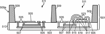
도 1a는 상단 포트형(top-ported) MEMS 마이크로폰 패키지(100)의 상부 사시도를 개략적으로 도시한 것이다. 도 1b는 도 1a에 도시된 상단 포트형 MEMS 마이크로폰 패키지(100)의 저면 사시도를 개략적으로 도시한 것이다. 도 1c, 1e 및 도 1f는 도 1a의 상단 포트형 MEMS 마이크로폰 패키지(100)의 라인 A-A를 따른 단면도의 다양한 예를 개략적으로 도시한 것이다. 도 1d는 도 1a의 상단 포트형 MEMS 마이크로폰 패키지(100)의 라인 B-B를 따른 단면도의 다양한 예를 개략적으로 도시한 것이다. MEMS 마이크로폰 패키지(100)는 다양한 응용예에 사용할 수 있다. 예를 들어, MEMS 마이크로폰 패키지(100)는 휴대 전화, 유선 전화, 컴퓨터 장치, 비디오 게임, 보청기, 청력 장치, 생체 보안 시스템, 양방향 무선기, 공개 발표 시스템 및 신호를 변환하는 기타 장치와 함께 사용될 수 있다. MEMS 마이크로폰 패키지(100)는 약 0.9mm와 2mm 사이의 제1 치수(D1)(예컨대, 두께), 약 2mm와 7mm 사이의 제2 치수(D2)(예컨대, 깊이) 및 약 3mm와 10mm 사이의 제3 치수(D3)(예컨대, 폭)를 가질 수 있다.1A schematically illustrates a top perspective view of a top-ported
도 1a를 참조하면, MEMS 마이크로폰 패키지(100)는 덮개(101) 및 덮개(101)를 통해 형성된 음향 입력 포트(103)를 포함한다. 덮개(101)는 아래에 더 상세히 설명되는 바와 같이 사출 성형된 열가소성 컴포넌트 또는 전자 회로 트레이스가 통합된 라미네이트 기판일 수 있다. 도 1c에 도시되어 있는 바와 같이, 덮개(101)는 내부에 속이 빈 공동이 형성되어 있다. 덮개(101)는 기판 층(105)에 결합되어 밀봉된 공동을 형성한다. 기판 층(105)은, 예를 들어 FR-4와 같은 인쇄 회로 기판(PCB) 재료를 포함하는 라미네이트 기판일 수 있다. 다른 예에서, 기판 층(105)은 프리몰딩된 리드프레임 타입 패키지("프리몰딩된 패키지"라고도 함)일 수 있다. 기판 층(105)의 다른 예는 세라믹 공동 패키지(ceramic cavity packages)를 포함한다.Referring to FIG. 1A, the
도 1c에 도시된 바와 같이, MEMS 마이크로폰 다이(107)는 음향 포트 개구(103)에 인접한 또는 이를 덮는 덮개(101)에 장착되어, 음향 입력 포트(103)를 통해 MEMS 마이크로폰 패키지(100)로 들어가는 음압(예컨대, 음파)이 MEMS 마이크로폰 다이(107)와 연관되거나 또는 상호작용하여 전기신호를 생성하고, 이 전기 신호는 추가적인(외부 및/또는 내부) 컴포넌트(예컨대, 스피커 및 수반 회로)에 의해 입력 음압에 대응하는 출력 가청 신호를 생성한다. MEMS 마이크로폰 다이(107)는 접착제나 당해 기술분야에서 공지되어 있는 다른 결합 메커니즘에 의해 덮개(101)에 장착될 수 있다.As shown in FIG. 1C, the MEMS microphone die 107 is mounted to a
전도성 트레이스(109)(예컨대, 금속 트레이스)가 덮개(101) 내부면의 적어도 일부분 상에 증착된다. 기판 층(105)이 (예컨대, 당해 분야에서 공지되어 있는 전도성 또는 비전도성 밀봉제를 통해) 덮개(101)에 밀봉될 때, 전도성 트레이스(109)는 기판 층(105) 상에 형성된 대응 트레이스(111)와 전기적으로 결합된다. 도 1c에 도시된 바와 같이, 기판 층(105) 상의 회로 트레이스(111)는 하나 이상의 전도성 비아(113)에 결합되고, 이 비아는 다시 기판 층(105) 하부 면 상의 하나 이상의 전기 접촉 패드(115)에 연결된다. 전기 접촉 패드(115)는 도 1b의 저면 사시도에 보다 상세히 도시되어 있다. 전기 접촉 패드(115)는 또한 패키지 입력/출력(I/O) 패드라고도 하며, 메인 보드, 인쇄 회로 기판, 또는 다른 전기적 상호접속 장치와 같은 다른 기판에 MEMS 마이크로폰 패키지(100)를 전기적으로 연결한다. 전기 접촉 패드(115)는 MEMS 마이크로폰 패키지(100)를 위한 전력 및 신호 연결을 제공할 수 있다.A conductive trace 109 (eg, metal trace) is deposited on at least a portion of the inner surface of the
도 1d는 덮개(101)의 내부면의 상세도이며, 상단 포트형 MEMS 마이크로폰 패키지(100)의 도 1a의 라인 B-B를 따른 단면도를 나타낸다. 전술한 바와 같이, 덮개(101)의 내벽에 증착된 전도성 트레이스(109)는 덮개(101)와 기판 층(105) 사이에 전기적 라우팅을 제공한다. 그러나, 이 예에서, 덮개(101)와 기판 층(105) 사이의 전기적 라우팅에 사용되지 않는 덮개(101)의 내부면은 기판 층(105)에 접지되는 전도성 층(119)으로 덮여있다. 전도성 층(119)은 기판 층(105)(전도성 접지판을 포함할 수도 있음)과 함께 MEMS 마이크로폰 패키지(100)의 개선된 전자기 차폐를 제공하는 패러데이 케이지(Faraday's cage)를 형성한다. 일부 예에서, 전도성 층(119)은 추가로 또는 대안적으로 덮개(101)의 외부면에 또는 그 주위에 위치할 수 있으며, 전도성 층(119)은 기판(105)의 접지에 결합되어 MEMS 마이크로폰 패키지(100)의 전자기 차폐를 제공한다. 이러한 예에서, 전도성 층(119)은 덮개(101)를 균일하게 코팅하는 단일 층일 수도 있고, 또는 덮개(101)의 소우 스트리트(saw-streets)를 따라 배열된 비아의 형태를 취할 수도 있다. 도 1c에 도시된 바와 같이, 와이어(117)는 MEMS 마이크로폰 다이(107)로부터 연장되어 MEMS 마이크로폰 다이(107)를 덮개(101)의 내부면 상에 형성된 전도성 트레이스(109)에 연결한다. 이와 같이, MEMS 마이크로폰 다이(107)는, 이 예에서 MEMS 마이크로폰 패키지(100)의 외부면에 전기 접촉 패드(115)를 포함하는 기판 층(105) 상에 장착된 하나 이상의 장치와 전자 통신한다.1D is a detailed view of the inner surface of the
도 1c의 예에서, MEMS 마이크로폰 다이(107)는 모놀리식 집적형 MEMS 다이이며, 이는 단일 다이 내에 ASIC(application specific integrated circuit) 컴포넌트 및 마이크로 기계식 전기 마이크로폰 다이어프램을 모두 포함한다. 그러나, 도 1e의 예에 도시된 바와 같이, 마이크로 기계식 전기 마이크로폰 다이어프램 및 ASIC 컴포넌트는 별도의 집적 회로로서 제공될 수도 있다. 예를 들어, 도 1e에 도시된 바와 같이, 덮개(101)가 MEMS 마이크로폰 다이(107')(마이크로 기계식 전기 마이크로폰 다이어프램을 포함함) 및 ASIC(121)을 모두 구비한다. 즉, MEMS 마이크로폰 다이(107')는 음향 입력 포트(103)에 인접한 또는 그 위에 있는 덮개(101)에 장착되고, ASIC(121) 또한 MEMS 마이크로폰 다이(107')에 인접한 덮개(101)의 내부면에 장착된다. 일부 예에서, ASIC(121)은 캡슐화(예컨대, 글로브 탑)로 커버될 수 있다. MEMS 마이크로폰 다이(107') 및 ASIC(121)은 접착제 또는 다른 결합 메커니즘에 의해 덮개(101)에 장착될 수 있다. 와이어(117)는 공동이 밀봉될 때 MEMS 마이크로폰 다이(107')와 ASIC(121)을 서로 전기접속하고, 또한 기판 층(105)(및 결과적으로 전기 접촉 패드(115))에 전기 접속한다.In the example of FIG. 1C, the MEMS microphone die 107 is a monolithic integrated MEMS die, which includes both application specific integrated circuit (ASIC) components and micromechanical electrical microphone diaphragms in a single die. However, as shown in the example of FIG. 1E, the micromechanical electric microphone diaphragm and ASIC components may be provided as separate integrated circuits. For example, as shown in FIG. 1E, the
도 1f는 상단 포트형 MEMS 마이크로폰 패키지(100)를 도 1a의 라인 A-A를 따라 절취한 다른 예의 단면도이다. 덮개(101) 및 기판 층(105)은 MEMS 마이크로폰 다이(107') 및 ASIC(121)(MEMS 마이크로폰 다이(107')를 제어하고 구동하는데 사용됨)을 수용하기 위한 내부 챔버를 형성한다. 다른 예들에서, ASIC(121) 및 MEMS 마이크로폰 다이(107')는 (예컨대,도 1c의 예에서와 같이) 단일 다이 내에 통합될 수 있다.1F is a cross-sectional view of another example of the top port type
도 1a 내지 도 1f는 상단 포트형 MEMS 마이크로폰 패키지(100)의 예를 도시하고 있지만, 일부 마이크로폰 패키지는 도 2a 내지 2c의 예에서와 같이 기판 층(105)을 통해 음향 입력 포트(103)를 위치시켜 하단 포트형 MEMS 마이크로폰 패키지(200)를 형성한다. 도 2a는 하단 포트형(bottom-ported) MEMS 마이크로폰 패키지(200)의 상부 사시도를 개략적으로 도시한 것이다. 마찬가지 방식으로, 도 2b는 도 2a에 도시된 하단 포트형 MEMS 마이크로폰 패키지(200)의 저면 사시도를 개략적으로 도시한 것이다. 도 2c는 도 2a의 하단 포트형 MEMS 마이크로폰 패키지(200)를 라인 C-C를 따라 절취한 단면도를 개략적으로 도시한 것이다. 도 2a에 도시된 바와 같이, MEMS 마이크로폰 패키지(200)는 제1 치수(D1)(예컨대, 두께), 제2 치수(D2)(예컨대, 깊이) 및 제3 치수(D3)를 가질 수 있으며, 이들은 제각기 도 1a에 도시된 MEMS 마이크로폰 패키지(100)의 제1 치수(D1), 제2 치수(D2) 및 제3 치수(D3)와 유사할 수 있다.1A-1F illustrate an example of a top ported
도 2a 및 2b를 참조하면, MEMS 마이크로폰 패키지(200)는 덮개 컴포넌트(201)뿐만 아니라 기판 층(205)을 통해 형성된 음향 입력 포트(203)를 포함한다. 덮개(201)는 기판 층(205)에 결합(예컨대, 접착)되어 밀봉된 공동을 형성한다. 기판 층(205)은 도 1a 내지 1f를 참조하여 전술한 기판 층(105)과 유사한 재료를 포함할 수 있다. 도 2c에 도시된 바와 같이, MEMS 마이크로폰 다이(207')(마이크로 기계식 전기 마이크로폰 다이어프램을 포함함)는 음향 포트 개구(203)에 인접한 또는 이를 덮는 기판 층(205)에 장착되어, 음향 입력 포트(203)를 통해 MEMS 마이크로폰 패키지(200)로 들어가는 음압(예컨대, 음파)이 MEMS 마이크로폰 다이(207)와 연관되거나 또는 상호작용하여 전기신호를 생성하고, 이 전기 신호는 추가적인(외부 및/또는 내부) 컴포넌트(예컨대, 스피커 및 수반 회로)에 의해 입력 음압에 대응하는 출력 가청 신호를 생성한다. MEMS 마이크로폰 다이(207')는 접착제나 당해 기술분야에서 공지되어 있는 다른 결합 메커니즘에 의해 기판 층(205)에 장착될 수 있다. 덮개(201)는 MEMS 마이크로폰 다이(207')를 전자기 간섭으로부터 차폐하기 위해 하나 이상의 금속 또는 다른 전도성 재료로 형성될 수 있다.2A and 2B, the
기판 층(205) 상의 회로 트레이스(211)는 하나 이상의 전도성 비아(213)에 결합되고, 이 비아는 다시 기판 층(205) 하부 면 상의 하나 이상의 전기 접촉 패드(215)에 연결된다. 기판(205)의 하부면 상의 전기 접촉 패드(215)는 또한 도 2b의 저면 사시도에 도시되어 있다. 전기 접촉 패드(215)는 메인 보드, 인쇄 회로 기판, 또는 다른 전기적 상호접속 장치와 같은 다른 기판에 MEMS 마이크로폰 패키지(200)를 전기적으로 연결한다. 전기 접촉 패드(215)는 또한 패키지 입력/출력(I/O) 패드라고도 하며, MEMS 마이크로폰 패키지(200)에 전력 및 신호 접속을 제공할 수 있다. 와이어(217)는 ASIC(221)(MEMS 마이크로폰 다이(207')를 제어하고 구동하는데 사용됨) 및 MEMS 마이크로폰 다이(207')를 서로 연결한다. 와이어(217)는 또한 ASIC(221)을 기판(205)상의 회로 트레이스(211)에 연결하는 역할을 한다. 일부 예에서, ASIC(221)은 캡슐화(예컨대, 글로브 탑)로 커버될 수 있다. 다른 예에서, ASIC(221) 및 MEMS 마이크로폰 다이(207')는 모놀리식 집적형 MEMS 다이(예컨대, 도 1a의 예에서와 같이)로서 제공될 수 있다.Circuit traces 211 on the
도 1a 내지 1f 및 도 2a 내지 2c와 관련하여 위에서 설명한 MEMS 마이크로폰 패키지(100 및 200)의 일반적인 구조로부터, 상단 포트형 MEMS 마이크로폰 패키지 및 하단 포트형 MEMS 마이크로폰 패키지는 제각기의 제조에 대해 상이한 BOM(bill of material) 및 공정 단계를 필요로 한다는 것을 알 수 있다. 즉, 상단 포트형 MEMS 마이크로폰 패키지(100) 및 하단 포트형 MEMS 마이크로폰 패키지(200)는 상이한 제조 단계를 가지며, 최종 MEMS 마이크 패키지를 제조하는데 필요한 원료, 서브 어셈블리, 중간 어셈블리, 서브 컴포넌트, 부품 및 수량도 각각 상이하다. 예를 들어, 상단 포트형 MEMS 마이크로폰 패키지(100)는 2개의 라미네이트 기판(예컨대, 기판 층(105)용의 하나의 라미네이트 기판과 덮개(101)용의 다른 하나의 라미네이트 기판)을 사용할 필요가 있는 반면에, 하단 포트형 MEMS 마이크로폰 패키지(200)는 하나의 라미네이트 기판(예컨대, 기판 층(205)용)과 하나의 금속 덮개(201)를 필요로 한다. 또한 현재 사용 가능한 MEMS 마이크로폰 패키지는 상단 포트형 또는 하단 포트형이다. 즉, 현재 시장은 상단 포트형 또는 하단 포트형의 단일 패키지 솔루션만 제공한다.From the general structure of the MEMS microphone packages 100 and 200 described above with respect to FIGS. 1A to 1F and 2A to 2C, the upper port type MEMS microphone package and the lower port type MEMS microphone package have different bills of bill (BOMs) for the manufacture of each. of materials) and process steps. That is, the upper port type
현재 이용 가능한 단일 패키지 솔루션은 마이크로폰 어레이의 제조를 복잡하게 할 수 있다. 도 3은 메인 보드(301)(예컨대, PCB) 및 메인 보드(301) 상에 배치된(예컨대, 장착되어 전기적으로 연결된) 복수의 MEMS 마이크로폰 패키지(303)를 포함하는 마이크로폰 어레이(300)의 평면도를 도시한 것이다. 마이크로폰 어레이(300)는, 예를 들어 스마트 소비자 제품 및/또는 음성 인식, 명령 캡처 및 인식, 또는 잡음 억제 중 적어도 하나에 사용될 수 있다. 도 3의 예는 MEMS 마이크로폰 패키지(303)의 원형 어레이를 도시하지만, MEMS 마이크로폰 패키지(303)의 다른 공간적 배열(예컨대, 선형 어레이 또는 매트릭스)도 가능할 수 있음에 유의하라. 복수의 MEMS 마이크로폰 패키지(303) 각각은 도 1a의 상단 포트형 MEMS 마이크로폰 패키지(100)나 도 2a의 하단 포트형 MEMS 마이크로폰 패키지(200)로 식별될 수 있다. 달리 말하면, 마이크로폰 어레이(300)의 복수의 MEMS 마이크로폰 패키지(303)는 전부 상단 포트형 MEMS 마이크로폰 패키지일 수도 있고 또는 전부 하단 포트 MEMS 마이크로폰 패키지일 수도 있으며, 또는 이들의 조합일 수도 있다. 마이크로폰 어레이(300)에서 상단 포트형 MEMS 마이크로폰 패키지 및/또는 하단 포트형 MEMS 마이크로폰 패키지(다른 BOM을 갖는)를 사용하면 제조 및 셋업이 복잡해져서 제조 비용이 증가할 수 있다. 이는 복수의 MEMS 마이크로폰 패키지(303)가 상단 포트형 MEMS 마이크로폰 패키지 및 하단 포트형 MEMS 마이크로폰 패키지의 조합을 포함하는 예에서(예컨대, 상이한 BOM이 요구되기 때문에) 특히 그러하다. 또한, 복수의 MEMS 마이크로폰 패키지(303)가 메인 보드(301)에 장착되기 때문에, 상단 포트형 MEMS 마이크로폰 패키지의 음향 입력 포트(103)는 메인 보드(301)의 주 표면(305)(예컨대, 상부 또는 위쪽 면)으로부터 멀어지는 쪽을 향하는 반면에, 하단 포트형 MEMS 마이크로폰 패키지의 음향 입력 포트(203)는 메인 보드(301)의 주 표면(305)을 향할 수 있다(그리고 메인 보드(301)의 두께를 통해 연장될 수 있다). 결과적으로, 도 3의 마이크로폰 어레이(300)는 복수의 MEMS 마이크로폰 패키지(303)에 측면으로(예컨대, 옆으로) 도달하는 음파(307)에 충분히 민감하지 않을 수 있다. 바꾸어 말하면, 도 3의 마이크로폰 어레이(300)는 복수의 MEMS 마이크로폰 패키지(303)의 덮개(101, 201)의 측벽에 입사하는 음파(307)를 적절하게 캡처하지 못할 수 있다. 이 시나리오에 대한 현재의 해결책은, 복수의 MEMS 마이크로폰 패키지(303)가 음파(307)를 검출할 수 있도록 하기 위해 복수의 MEMS 마이크로폰 패키지(303)의 상향 또는 하향 음향 입력 포트(103, 203)로 음파(307)를 안내하기 위해 음파(307)를 메인 보드(301)의 상부면 및/또는 하부면으로 채널링하는 추가 기능부(예컨대, 사운드 가이드)를 사용하는 것이다. 그러나, 이러한 해결책은 마이크로폰 어레이(300)의 제조와 관련된 비용 및 복잡성을 더욱 증가시킨다. 또한, 마이크로폰 어레이(300)는 일반적으로 패키지 수준이 아니라 보드 수준에서(예컨대, 복수의 MEMS 마이크로폰 패키지(303)를 메인 보드(301) 상에 장착함으로써) 생성되기 때문에, 마이크로폰 어레이(300)는 일반적으로 모바일 애플리케이션에서의 구현을 제한할 수 있는 면적을 차지한다. 이들 사항을 감안할 때, (1) 크기가 작고(예컨대, 작은 패키지 풋프린트를 가짐); (2) 표준 BOM을 가지면서 상단 포트형 MEMS 마이크로폰 패키지, 하단 포트형 MEMS 마이크로폰 패키지 또는 측면 포트형 MEMS 마이크로폰 패키지가 되도록 쉽게 구성할 수 있으며; (3) 패키지 수준에서 다른 유사한 MEMS 마이크로폰 패키지와 쉽게 결합되어 모바일 애플리케이션에 적합한 소형 마이크로폰 어레이를 형성하도록 모듈식으로 설계되고; (4) 추가 기능부(예컨대, 사운드 가이드)를 사용하지 않고도 MEMS 마이크로폰 패키지로 측면으로(옆으로) 이동하는 음파에 민감한 개선된 MEMS 마이크로폰 패키지에 대한 요구가 있을 수 있다.The single package solutions currently available can complicate the manufacture of microphone arrays. 3 is a top view of a
도 4a 내지 4c 및 도 5a 내지 5f는 일 실시예에 따른, MEMS 마이크로폰 패키지 제조 방법을 도시한 공정 흐름을 보여준다. 도 4a 내지 4c 및 도 5a 내지 5f의 공정 흐름을 이용하여 제조할 수 있는 예시적인 MEMS마이크로폰 패키지가 도 7a, 7b, 8a 및 8b에 도시되어 있다. MEMS 마이크로폰 패키지는 측면으로 이동하는 음파에 민감한 MEMS 마이크로폰 어레이를 (모듈식 방식으로 그리고 패키지 수준에서) 편리하고 저렴하게 제조하는데 사용될 수 있다. 도 7a, 7b, 8a 및 8b의 MEMS 마이크로폰 패키지를 사용하여 제조될 수 있는 예시적인 MEMS 마이크로폰 어레이가 도 9a 내지 9e 및 10a 내지 10e에 도시되어 있다.4A to 4C and 5A to 5F show a process flow showing a method of manufacturing a MEMS microphone package, according to an embodiment. Exemplary MEMS microphone packages that can be prepared using the process flows of FIGS. 4A-4C and 5A-5F are shown in FIGS. 7A, 7B, 8A, and 8B. The MEMS microphone package can be used to conveniently and inexpensively manufacture a modular array of MEMS microphones (modularly and at the package level) that are sensitive to sound waves traveling laterally. Exemplary MEMS microphone arrays that can be manufactured using the MEMS microphone packages of FIGS. 7A, 7B, 8A, and 8B are shown in FIGS. 9A-9E and 10A-10E.
일부 실시예에 따른 MEMS 마이크로폰 패키지의 제1 부분(413)의 형성을 도시한 도 4a 내지 도 4c를 먼저 참고하면, 도 4a는 MEMS 마이크로폰 패키지를 위한 프레임(401)을 도시한 것이다. 프레임(401)은 (예컨대, 후술하는 바와 같이 싱귤레이션 후에) 조립형 MEMS 마이크로폰 패키지에서 하나 이상의 덮개를 형성하는 부분을 포함한다. 프레임(401)은 프레임(401)을 통해 연장되는 하나 이상의 포트(405)(예컨대, 궁극적으로는 조립형 MEMS 마이크로폰 패키지의 음향 입력 포트를 형성함)를 가질 수 있다. 프레임(401)은 또한 프레임(401)의 한 쪽에 형성된 블리드 스톱 릿지(bleed stop ridge)(403)를 갖는다. 블리드 스톱 릿지(403)는 프레임(401)의 상부 표면 상의 융기부일 수 있고, 각각의 블리드 스톱 릿지(403)는 제각기의 포트(405)를 둘러싸도록 형성될 수 있으며, 프레임(401)의 상부 표면에 도포된 재료가 흘러내리지 않도록 또는 블리드 스톱 릿지(403) 외부로 흐르지 않도록 방지하는 물리적 장벽을 제공할 수 있다.Referring first to FIGS. 4A-4C showing the formation of the
일부 실시예들에서, 프레임(401)은 조립형 MEMS 마이크로폰 패키지에 대한 전자기 간섭(EMI)을 차폐하기 위해 전도성 재료로 형성될 수 있다. 일부 실시예에서, 프레임(401)은 구리, 금, 알루미늄 또는 다른 금속 또는 합금으로 제조될 수 있으며, 몰딩(molding), 화학 또는 플라즈마 에칭, 밀링, 스탬핑 또는 다른 제조 공정에 의해 형성될 수 있다. 다른 실시예에서, 프레임(401)은 내부에 전도성 재료가 있는 몰딩 컴파운드와 같은 전도성 재료, 또는 에폭시, 몰딩 컴파운드 등과 같은 전도성 중합체로 제조될 수 있다.In some embodiments, the
도 4b는 일부 실시예에 따라 프레임(401) 상에 MEMS 마이크로폰 다이(407)를 장착하여 MEMS 마이크로폰 패키지의 제1 부분(413)을 형성하는 것을 도시한 것이다. 아교, 에폭시, 다이 부착 필름(DAF) 등과 같은 접착제(411)를, 접착제(411)를 포함하는 블리드 스톱 릿지(403) 내의 프레임(401)의 상부 표면에 바른다. 블리드 스톱 릿지(403)는 접착제(411)가 상이한 덮개 또는 패키지에 대해 지정된 영역 사이로 흐르는 것을 방지한다. 일부 실시예에서, MEMS 마이크로폰 다이(407)가 접착제(411) 상에 장착되며(이후에 경화될 수 있음), 따라서 MEMS 마이크로폰 다이(407)는 프레임(401)의 상부 표면에 고정된다. 일부 실시예들에서, 각각의 MEMS 마이크로폰 다이(407)는 제각기의 포트(405)에 걸쳐있는 프레임(401)에 부착될 수 있다. MEMS 마이크로폰 다이들(407) 각각은 제각기의 MEMS 마이크로폰에 대한 프론트 챔버(front chamber) 또는 프론트 볼륨(front volume) 역할을 하는 센서 공동(415)을 가질 수 있다.4B illustrates mounting a MEMS microphone die 407 on a
도 4c는 일부 실시예에 따른 차폐된 MEMS 마이크로폰 패키지의 제1 부분(413) 상에 상호접속부(421 및 423)를 장착한 것을 도시한 것이다. 상호접속부(421 및 423)는, 프레임(401) 상에 장착되며 프레임(401)과 전기적으로 접촉하는 프레임 상호접속부(423)를 포함할 수 있다. 일부 실시예에서, 프레임 상호접속부(423)는 블리드 스톱 릿지(403) 또는 프레임(401)의 다른 노출된 부분 상에 장착되며, 프레임(401) 또는 덮개를 접지시킬 수 있다. 상호접속부(421 및 423)는 또한 MEMS 마이크로폰 다이(407)의 상부면 상에 배치된 다이 랜딩 패드(409) 상에 장착된 다이 상호접속부(421)를 포함할 수 있다. 상호접속부(421 및 423)는, 예를 들어 전기 불꽃(electric flame-off)을 사용하여 노출된 와이어의 단부에서 볼을 형성하는 와이어본드 머신을 이용하여 형성되는 와이어 본드 구조일 수 있으며, 예를 들어, 열, 압력 및/또는 초음파 진동을 이용하여 상호접속부의 볼 단부를 블리드 스톱 릿지(403) 및 다이 랜딩 패드(409)에 용접하거나, 용융하거나 또는 다른 방식으로 부착할 수 있다. 와이어의 볼 단부가 접촉 패드(115)에 부착된 후에, 와이어본딩 머신이 와이어를 절단하여 상호접속부(421 및 423)의 제2 단부를 형성할 수 있다. 상호접속부(421, 423)는 프레임(401) 또는 MEMS 마이크로폰 다이(407) 상에 위치하는 제1 단부를 가지며, 프레임(401)으로부터 멀어지도록 연장된다. 상호접속부(421 및 423)의 제2 단부는 상호접속부(421 및 423)의 제1 단부에 대향한다. 일부 실시예에서, 상호접속부(421 및 423)의 제2 단부는 제1 부분(413) 위에 기판의 후속 장착을 용이하게 하기 위해 높이가 실질적으로 같거나 또는 동일 평면에 있다. 다른 실시예에서, 상호접속부(421 및 423)는 솔더 볼, 지지 구조물을 갖는 솔더 볼, 접촉 패드 상에 위치하는 미리 형성된 구조물, 인쇄 구조물 또는 프레임(401) 상에 배치된 구조물 또는 다이 랜딩 패드(409)이다.FIG. 4C illustrates mounting of
이제 도 5a 내지 도 5f를 참조하며, 이들 도면은 일부 실시예에 따른 MEMS 마이크로폰 패키지의 제2 부분을 형성하는 것을 도시한 것이다. 도 5a는 차폐된 MEMS 마이크로폰 패키지의 제2 부분(501)을 나타내며, 제2 부분(501)은 기판(513)(예컨대, PCB)의 주 표면에 배치된 하나 이상의 패드(505)(예컨대, 랜딩 패드)를 갖는다. 하나 이상의 패드(505)는 기판(513) 또는 기판 본체(503)에 하나 이상의 금속 라인 및/또는 비아(507)에 의해 상호접속될 수 있다. 하나 이상의 금속 라인 및/또는 비아(507)는 조립형 MEMS 마이크로폰 패키지에 대한 전력 및 신호 접속을 제공하도록 구성될 수 있음에 유의하라.Reference is now made to FIGS. 5A-5F, which illustrate forming a second portion of a MEMS microphone package in accordance with some embodiments. 5A shows the
도 5b는 일부 실시예에 따른 제2 부분(501) 상에 측벽(509)을 형성한 것을 도시한 것이다. 일부 실시예에서, 측벽(509)은 기판 본체(503) 상에 형성되고, 다른 실시예에서, 측벽(509)은 기판(513)의 표면 상에 위치하는 스토퍼 패드, 산화물 또는 밀봉층 등에 형성될 수 있다. 일부 실시예에서, 측벽(509)은 도금 공정에 적합한 몰딩 컴파운드로 형성된다. 예를 들어, 측벽(509)은 엘라스토머 몰딩 컴파운드 재료를 포함할 수 있고, 측벽(509)의 외부 표면(509a)은 전도성 재료(예컨대, 구리)로 도금되어 전기 접촉 패드(패키지 입력/출력I/O) 패드라고도 함)를 형성할 수 있으며, 전기 접촉 패드는 조립형 MEMS 마이크로폰 패키지에 전력 및 신호 접속을 제공하고 기판 본체(503)에 배치된 하나 이상의 금속 라인 및/또는 비아(507)에 전기적으로 결합된다. 이 단계는 도 6d 및 6e에서 보다 상세하게 설명한다. 측벽(509)은 적절한 위치에 측벽을 몰딩하고, 3D 프린팅하며, 측벽(509)을 미리 형성하고, 측벽(509)을 기판(513)에 부착함으로써 또는 다른 제조 공정에 의해 형성될 수 있다. 측벽(509)은 다이 영역 및 하나 이상의 패드(505)를 연속적으로 둘러싸도록 형성되고, 기판(513)으로부터 멀어지도록 연장되어 내부 공동(511)을 제공한다.5B illustrates the formation of
도 5c는 일부 실시예에 따른 제어 칩(515)의 부착을 도시한 것이다. 제어 칩(515)은 ASIC, 통신 장치, 인터페이스 장치 등일 수 있고, MEMS 마이크로폰 다이(407)를 제어하거나 또는 판독하는 회로를 가질 수 있다. 제어 칩(515)은 DAF, 접착제, 테이프 등과 같은 다이 부착 구조(519)에 의해 기판(513)에 부착된다. 다른 실시예에서, 제어 칩(515)은 클립, 소켓, 스크류 등과 같은 기계적 리테이너로 기판(513)에 부착된다. 제어 칩(515)은 기판(513)에서 먼 쪽의 상부면에 배치된 하나 이상의 제어 칩 본드 패드(517)를 갖는다. 도 5d는 일부 실시예에 따른 제어 칩(515)을 하나 이상의 패드(505)에 와이어 본딩하는 것을 도시한 것이다. 일부 실시예에서, 제어 칩(515)은 와이어 본드 제어 칩이고 와이어본드 접속(523)을 이용하여 하나 이상의 패드(505)에 전기적으로 연결된다. 도 5c 및 5d는 제어 칩(515)이 기판(513)에 와이어본딩될 수 있음을 나타내지만, (도 5e의 예에서와 같이) 패드 장착 제어 칩도 가능하다.5C illustrates attachment of a
도 5e는 일부 실시예에 따른 패드 장착 제어 칩(529)을 부착한 것을 도시한 것이다. 전도성 커넥터(527)가 하나 이상의 패드(505)에 부착될 수 있다. 일부 실시예에서, 패키지는 제어 칩(529)의 하부면에 부착 패드(531)가 장착되는 제어 칩(529)을 포함한다. 패드 장착 제어 칩(529)은 전도성 커넥터(527)에 의해 패드(505)에 부착된다. 패드 장착 제어 칩(529)은 ASIC, 통신 장치, 인터페이스 장치 등일 수 있고, MEMS 마이크로폰 다이(407)를 제어하거나 또는 판독하는 회로를 가질 수 있다. 도 5e에 도시되어 있는 차폐 센서 패키지의 제2 부분(501)은 와이어본딩된 제어 칩(515) 및 패드 장착 제어 칩(529)과 함께 도시되어 있지만, 이들 상이한 유형의 제어 칩(515 및 529)은 단지 예시를 위한 것으로 제한적인 것은 아니다. 도 5f는 일부 실시예에 따른 덮개 커넥터(537)를 측벽(509)에 붙이는 것을 도시한 것이다. 덮개 커넥터는 측벽(509)의 제2 단부에 배치되며, 접착제, DAF, 에폭시 또는 다른 접착제 또는 부착 구조일 수 있다.5E illustrates attaching a pad mounting
도 6a 내지 도 6e는 일부 실시예에 따른, 차폐 MEMS 마이크로폰 패키지(600)의 조립체를 도시한 것이다. 도 6a는 도 4c의 제1 부분(413)을 도 5f의 제2 부분(501)에 부착한 것을 도시한 것이다. 제1 부분(413)은 뒤집어져서 내부 공동(511)을 둘러싸도록 덮개 커넥터(537)에 의해 제2 부분(501)에 부착된다. 또한, 상호접속부(421 및 423)는 제2 부분의 패드(505)에 부착되고 전도성 커넥터(527)에 의해 고정된다. 일부 실시예에서, 패드(505)의 상부 표면은 실질적으로 수평이며, 따라서 상호접속부(421 및 423)의 단부가 제각기의 패드(505)와 일제히 접촉한다. 일부 실시예에서, 각각의 상호접속부(421 및 423)는, 각각의 상호접속부(421 및 423)의 제2 단부가 기판(513)의 표면 상의 상이한 접촉 패드(505)와 전기적으로 접촉하도록, 차폐된 MEMS 마이크로폰 패키지(600)의 제1 부분(413)으로부터 연장된다. 다른 실시예에서, 하나 이상의 상호접속부(421 및 423)가 제어 칩 본드 패드(517) 또는 다른 랜딩 패드, 접촉 패드 등과 접촉한다. 따라서, MEMS 마이크로폰 다이(407)가 센서 상호접속부(421)를 통해 제각기의 제어 칩(515 및 529)에 연결될 수 있는 반면에, MEMS 마이크로폰 다이(407)와 제각기의 제어 칩(515 및 529)은 서로 이격되어 중첩된다. MEMS 마이크로폰 다이(407) 및 제각기의 제어 칩(515 및 529)의 공간적 중첩으로 패키지 풋프린트의 소형화를 달성할 수 있다. 도 6a에 도시된 바와 같이, 상호접속부(421)와 관련하여, 상호접속부(421)의 한 단부는 MEMS 마이크로폰 다이(407)의 다이 랜딩 패드(409)에 부착되고 다이 랜딩 패드(409)로부터 먼 쪽으로 연장된다. 상호접속부(421)의 다른 단부는 기판(513) 상의 랜딩 패드(505)와 접촉하고(예컨대, 전기적 접촉 및/또는 물리적 접촉), 랜딩 패드(505)는 기판 본체(503)에 배치된 하나 이상의 금속 라인 및/또는 비아(507)에 전기적으로 연결된다.6A-6E illustrate an assembly of a shielded
측벽(509) 및 프레임(401)은 제어 칩들(515 및 529) 및 MEMS 마이크로폰 다이(407)를 EMI 차폐하여 고립시키는 전도성 쉘을 형성한다. 일부 실시예들에서, 기판(513)은 또한 차폐 층(도시되지 않음)을 구비하여 MEMS 마이크로폰 패키지(600)의 EMI 차폐를 높인다. 또한, 도시된 구성에서, 내부 공동(511)은 MEMS 마이크로폰 다이(407)에 대한 백 볼륨(back volume)으로서 작용하는 반면, 센서 공동(415)은 프론트 볼륨으로서 작용한다. 제1 부분(413)이 제2 부분(501)에 장착된 후, 패키지(600)는 경화되거나 리플로우되거나 하여 덮개 커넥터(537) 및 전도성 커넥터(527)를 응고, 경화 또는 리플로우할 수 있다. MEMS 마이크로폰 패키지(600)는 또한 테이프 등과 같은 캐리어(539) 상에 장착될 수 있다.The
도 6b는 일부 실시예에 따른, MEMS 마이크로폰 패키지(600)의 싱귤레이션을 도시한 것이다. MEMS 마이크로폰 패키지(600)는 다이 절단, 레이저 절단 등에 의해 절단되어 절단 영역(541)을 형성하고, 상기 캐리어(539) 상에 MEMS 마이크로폰 패키지(600)를 유지하면서, 개개의 패키지(600)를 분리한다. 도 6b의 예는 개별 패키지(600)를 형성하기 위한 싱귤레이션을 도시한 것이며, 여기서 각각의 MEMS 마이크로폰 패키지(600)는 단일 MEMS 마이크로폰 다이(407)를 포함하고, 도 6b의 싱귤레이션 공정은 도 6b의 구조는 도 6a의 구조가 싱귤레이트되어 개별 패키지(602)(예컨대, 도 6c에 도시된 단일 패키지(602))를 형성하도록 조정되거나 수정될 수 있으며, 여기서 각각의 MEMS 마이크로폰 패키지(602)는 복수의 MEMS 마이크로폰 다이(407)(예컨대, 도 6c의 예에서 2개의 MEMS 마이크로폰 다이(407))를 포함한다.6B illustrates singulation of a
도 5b를 참조하여 위에서 설명한 바와 같이, 측벽(509)은 엘라스토머 몰딩 컴파운드 재료를 포함할 수 있고, 측벽(509)의 외부 표면(509a)은 전도성 재료(예컨대, 구리)로 도금되어 전기 접촉 패드(패키지 입력/출력I/O) 패드라고도 함)를 형성할 수 있으며, 전기 접촉 패드는 조립형 MEMS 마이크로폰 패키지(600)에 전력 및 신호 접속을 제공하고 기판 본체(503)에 배치된 하나 이상의 금속 라인 및/또는 비아(507)에 전기적으로 결합된다. 도 6d에 도시된 바와 같이, 도 6b의 각각의 싱귤레이션된 MEMS 마이크로폰 패키지(600)는 캐리어(539)로부터 선택되어 캐리어(539') 상으로 재배치되며, 이에 따라 각각의 싱귤레이션된 MEMS 마이크로폰 패키지(600)의 측벽(509)의 제1 외부 표면(509a1)이 캐리어(539')와 접촉(예컨대, 물리적 접촉)하여 부착되는 한편, 측벽(509)의 제2 외부 표면(509a2)은 상향이며 캐리어(539')로부터 먼쪽을 향한다. 간략화를 위해 하나의 MEMS 마이크로폰 패키지(600)만이 도 6d에 도시되어 있다.As described above with reference to FIG. 5B,
도 6e에 도시된 바와 같이, 당해 분야에 공지되어 있는 도금 및 에칭 공정을 측벽(509)의 제2 외부 표면(509a2)에 대해 수행하여, 전기 접촉 패드(543)(패키지 입력/출력(I/O) 패드라고도 함) 및 트레이스(545)를 측벽(509)의 제2 외부 표면(509a2)에 형성되도록 할 수 있다. 트레이스(545)는 전기 접촉 패드(543)에 전기 및/또는 물리적으로 결합되며, 트레이스(545)는 측벽(509)의 제2 외부 표면(509a2)에 인접한 기판(513)의 표면(513a)에 형성되는 단자 부분(545a)을 갖는다. 도 6e에 도시된 바와 같이, 트레이스(545)는 또한 전기 접촉 패드(543)와 하나 이상의 금속 라인 및/또는 비아(507)를 서로 전기적으로 연결시키기 위해 기판(513)의 적어도 일부로 연장된다. 일부 실시예들에서, 기판(513) 내로 연장되는 트레이스(545)의 부분과 기판(513)의 표면(513a)에 배치된 트레이스(545)의 부분 사이의 각도는 약 90 도일 수 있다. 이어서 각각의 싱귤레이션된 MEMS 마이크로폰 패키지(600)가 캐리어(539')로부터 제거될 수 있다.As shown in FIG. 6E, a plating and etching process known in the art is performed on the second outer surface 509a2 of the
도 7a는 일부 실시예에 따른, 도 4a 내지 도 4c, 도 5a 내지 도 5f 및 도 6a 내지 도 6e에 도시된 공정을 사용하여 형성된 조립형 MEMS 마이크로폰 패키지(600)의 상부 등각도를 개략적으로 도시한 것이다. 도 7b는 도 7a에 도시된 MEMS 마이크로폰 패키지(600)의 하부 등각도를 개략적으로 도시한 것으로, MEMS 마이크로폰 패키지(600)의 하부면에 형성된 전기 접촉 패드(543) 및 트레이스(545)를 보다 상세히 도시하고 있다. 도 7c는 도 7a의 MEMS 마이크로폰 패키지를 라인 D-D를 따라 절취한 단면도를 개략적으로 도시한 것이다. 도 7a 내지 7c의 MEMS 마이크로폰 패키지(600)는 MEMS 마이크로폰 패키지(600)의 제1 측면(L1)(예컨대, 측벽)에 위치하는 단일 음향 입력 포트(405) 및 덮개(401)를 갖는 단일 MEMS 마이크로폰을 포함한다. MEMS 마이크로폰 패키지(600)의 제2 측면(L2)(제1 측면(L1) 반대쪽)은 기판(513)의 노출된 표면에 의해 형성될 수 있다. MEMS 마이크로폰 패키지(600)의 제3 측면(L3) 및 제4 측면(L4)은 측벽(509)의 몰딩 컴파운드에 의해 형성될 수 있다. 결과적으로, 도 7a 및 7b에 도시되어 있는 MEMS 마이크로폰 패키지(600)는 패키지(600)의 일 측면(예컨대, 측면(L1)) 상에 위치하는 하나의 측면 포트를 갖는 단일 MEMS 마이크로폰을 형성한다. 즉, 도 7a 및 7b에 도시되어 있는 MEMS 마이크로폰 패키지(600)는 패키지(600)의 하나의 측벽에 위치하는 하나의 사운드 포트를 갖는 단일 실리콘 마이크로폰을 형성한다. 도 7a에 도시된 바와 같이, MEMS 마이크로폰 패키지(600)는 약 2mm의 제1 치수(D1)(예컨대, 두께), 약 1mm의 제2 치수(D2)(예컨대, 깊이), 및 약 2mm의 제3 치수(D3)(폭)를 가질 수 있으며, 따라서 패키지 풋프린트가 (예컨대, 도 1a 및 2a의 예에 비해) 작아진다. 그러므로, 조립형 MEMS 마이크로폰 패키지(600)(및 그 제조 방법)는 다음의 이점, 즉, (1) 크기가 작고(예컨대, 작은 패키지 풋프린트를 가짐); (2) 표준 BOM을 가지며, 상단 포트형 MEMS 마이크로폰 패키지, 하단 포트형 MEMS 마이크로폰 패키지, 또는 측면 포트형 MEMS 마이크로폰 패키지로 쉽게 구성 가능하고; (3) 추가적인 기능부(예컨대, 사운드 가이드)를 사용하지 않고 MEMS 마이크로폰 패키지로 측면으로(옆으로) 이동하는 음파에 민감하다는 이점을 달성한다.FIG. 7A schematically depicts a top isometric view of a prefabricated
위에서 논의한 바와 같이, 도 6b의 싱귤레이션 공정은 도 6a의 구조가 싱귤레이션되어 개별 패키지(602)(예컨대, 도 6c에 도시된 단일 패키지(602))를 형성하도록 조정되거나 수정될 수 있으며, 여기서, 각각의 MEMS 마이크로폰 패키지(602)는 복수의 MEMS 마이크로폰 다이(407)(예컨대, 도 6c의 예에서 2개의 MEMS 마이크로폰 다이(407))를 포함한다. 도 8a 및 8b는 이러한 예를 도시한 것으로, 여기서 도 8a는 2개의 마이크로폰을 갖는 조립형 MEMS 마이크로폰 패키지(800)의 상부 등각도를 개략적으로 도시한 것이고, 도 8b는 도 8a에 도시된 MEMS 마이크로폰 패키지(800)의 하부 등각도를 개략적으로 도시한 것이다. 도 8b는 또한 MEMS 마이크로폰 패키지(800)의 하부 표면에 형성된 전기 접촉 패드(543) 및 트레이스(545)를 보다 상세하게 도시하고 있다.As discussed above, the singulation process of FIG. 6B can be adjusted or modified such that the structure of FIG. 6A is singulated to form individual packages 602 (eg, a
도 8a 및 8b의 MEMS 마이크로폰 패키지(800)는 MEMS 마이크로폰 패키지(800)의 제1 측면(L1)에 위치한 2개의 MEMS 마이크로폰 및 2개의 음향 입력 포트(405)를 포함한다. MEMS 마이크로폰 패키지(800)의 제3 측면(L3) 및 제4 측면(L4)은 측벽(509)의 몰딩 컴파운드에 의해 형성될 수 있다. MEMS 마이크로폰 패키지(800)의 제2 측면(L2)(제1 측면(L1)과 반대임)은 기판(513)의 노출된 표면에 의해 형성될 수 있다(도 8a의 라인 E-E를 따라 절취한 단면도는 도 7c와 유사함에 유의하라). 결과적으로, 도 8a 및 도 8b에 도시된 MEMS 마이크로폰 패키지(800)는 2개의 MEMS 마이크로폰을 가지며 패키지(800)의 한 쪽(예컨대, 측면(L1))에 2개의 측면 포트가 위치하는 마이크로폰 어레이를 형성한다. 달리 말하면, 도 8a 및 8b에 도시된 MEMS 마이크로폰 패키지(800)는 마이크로폰 패키지(800)의 하나의 측벽에 위치한 2개의 사운드 포트를 갖는 마이크로폰 어레이(보드 수준이 아닌 패키지 수준)를 형성한다. 도 8a에 도시된 바와 같이, MEMS 마이크로폰 패키지(800)는 약 2mm의 제1 치수(D1)(예컨대, 두께), 약 1mm의 제2 치수(D2)(예컨대, 깊이) 및 약 4mm의 제3 치수(D3)(예컨대, 폭)를 가질 수 있으며, 따라서 (예컨대, 도 3의 예와 비교하여) 마이크로폰 어레이 풋프린트가 작아질 수 있다. 그러므로, 조립형 MEMS 마이크로폰 패키지(800)(및 그 제조 방법)는 다음의 이점, 즉, (1) 크기가 작고(예컨대, 작은 패키지 풋프린트를 가짐); (2) 표준 BOM을 가지면서 상단 포트형 MEMS 마이크로폰 패키지, 하단 포트형 MEMS 마이크로폰 패키지 또는 측면 포트형 MEMS 마이크로폰 패키지가 되도록 쉽게 구성할 수 있으며; (3) 패키지 수준에서 다른 유사한 MEMS 마이크로폰 패키지와 쉽게 결합되어 모바일 애플리케이션에 적합한 소형 마이크로폰 어레이를 형성하도록 모듈식으로 설계되고; (4) 추가 기능부(예컨대, 사운드 가이드)를 사용하지 않고도 MEMS 마이크로폰 패키지로 측면으로(옆으로) 이동하는 음파에 민감하다는 이점을 달성한다.The
도 9a 내지 9b에 도시되어 있는 바와 같이, 도 7a 및 7b의 단일 MEMS 마이크로폰 패키지(600)가 다른 MEMS 마이크로폰 패키지(600)와 결합되어 양면(dual-side) 사운드 포트 마이크로폰 어레이를 형성할 수 있다. 도 9a 및 9b는 2개의 마이크로폰을 갖는 MEMS 마이크로폰 패키지(900)의 상부 등각도를 개략적으로 보여주며, 도 9c 및 9d는 각각 도 9a 및 9b에 도시된 MEMS 마이크로폰 패키지(900)의 하부 등각도를 개략적으로 보여준다. 또한, 도 9e는 도 9a의 라인 F-F를 따라 절취한 MEMS 마이크로폰 패키지(900)의 단면도를 도시한 것이다. 도 9e에 도시된 바와 같이, MEMS 마이크로폰 패키지(900)는 2개의 MEMS 마이크로폰 패키지(600)의 기판(513)을 (예컨대, 접착제에 의해) 서로 결합하여 형성될 수 있으며, 이에 따라 양면 사운드 포트 마이크로폰 어레이를 형성할 수 있다. 즉, 도 9a 내지 9e에 도시된 마이크로폰 어레이는 스테레오 구성을 갖는다.9A-9B, the single
도 9a 내지 9e의 MEMS 마이크로폰 패키지(900)는 하나의 MEMS 마이크로폰 및 MEMS 마이크로폰 패키지(900)의 제1 측면(L1) 및 제2 측면(L2) 각각에 위치하는 하나의 음향 입력 포트(405)를 포함한다. MEMS 마이크로폰 패키지(800)의 제3 측면(L3) 및 제4 측면(L4)은 측벽(509)의 몰딩 컴파운드에 의해 형성될 수 있다. 결과적으로, 도 9a 내지 9e에 도시된 MEMS 마이크로폰 패키지(900)는 제2 MEMS 마이크로폰 및 측면 포트(903)에 대향하여 위치하는 제1 MEMS 마이크로폰 및 측면 포트(901)를 갖는 마이크로폰 어레이를 형성한다. 달리 말하면, 도 9a 내지 9e에 도시된 MEMS 마이크로폰 패키지(900)는 (보드 수준이 아니라 패키지 수준에서) 서로에 대해 패키지(900)의 대향 측면에 위치하는 2개의 사운드 포트(405)를 갖는 마이크로폰 어레이를 형성한다. 도 9a에 도시된 바와 같이, MEMS 마이크로폰 패키지(800)는 약 2mm의 제1 치수(D1)(예컨대, 두께), 약 2.5mm의 제2 치수(D2)(예컨대, 깊이) 및 약 2mm의 제3 치수(D3)(예컨대, 폭)를 가질 수 있으며, 따라서 (예컨대, 도 3의 예와 비교하여) 마이크로폰 어레이 풋프린트가 작아질 수 있다. 그러므로, 조립형 MEMS 마이크로폰 패키지(900)(및 그 제조 방법)는 다음의 이점, 즉, (1) 크기가 작고(예컨대, 작은 패키지 풋프린트를 가짐); (2) 표준 BOM을 가지면서 상단 포트형 MEMS 마이크로폰 패키지, 하단 포트형 MEMS 마이크로폰 패키지 또는 측면 포트형 MEMS 마이크로폰 패키지가 되도록 쉽게 구성할 수 있으며; (3) 패키지 수준에서 다른 유사한 MEMS 마이크로폰 패키지와 쉽게 결합되어 모바일 애플리케이션에 적합한 소형 마이크로폰 어레이를 형성하도록 모듈식으로 설계되고; (4) 추가 기능부(예컨대, 사운드 가이드)를 사용하지 않고도 MEMS 마이크로폰 패키지로 측면으로(옆으로) 이동하는 음파에 민감하다는 이점을 달성한다.The
도 10a 내지 10b에 도시되어 있는 바와 같이, 도 8a 내지 8b의 MEMS 마이크로폰 어레이(800)는 다른 MEMS 마이크로폰 패키지(800) 와 결합되어 양면(dual-side) 사운드 포트 마이크로폰 어레이를 형성할 수 있다. 도 10a 및 10b는 4개의 마이크로폰을 갖는 MEMS 마이크로폰 패키지(1000)의 상부 등각도를 개략적으로 보여주며, 도 10c 및 10d는 각각 도 10a 및 10b에 도시된 MEMS 마이크로폰 패키지(1000)의 하부 등각도를 개략적으로 보여준다. 또한, 도 10e는 도 10a의 라인 G-G를 따라 절취한 MEMS 마이크로폰 패키지(1000)의 단면도를 도시한 것이다. 도 10e에 도시된 바와 같이, MEMS 마이크로폰 패키지(1000)는 2개의 MEMS 마이크로폰 패키지(800)의 기판(513)을 (예컨대, 접착제에 의해) 서로 결합하여 형성될 수 있으며, 이에 따라 양면 사운드 포트 마이크로폰 어레이를 형성할 수 있다. 즉, 도 10a 내지 10e에 도시된 마이크로폰 어레이는 스테레오 구성을 갖는다.10A-10B, the
도 10a 내지 10e의 MEMS 마이크로폰 패키지(1000)는 2개의 MEMS 마이크로폰 및 MEMS 마이크로폰 패키지(1000)의 제1 측면(L1) 및 제2 측면(L2) 각각에 위치하는 2개의 음향 입력 포트(405)를 포함한다. MEMS 마이크로폰 패키지(1000)의 제3 측면(L3) 및 제4 측면(L4)은 측벽(509)의 몰딩 컴파운드에 의해 형성될 수 있다. 결과적으로, 도 10a 내지 10e에 도시된 MEMS 마이크로폰 패키지(1000)는 제2 MEMS 마이크로폰 어레이(1002)에 대향하여 위치하는 제1 MEMS 마이크로폰 어레이(1001)를 갖는 마이크로폰 어레이를 형성한다. 달리 말하면, 도 10a 내지 10e에 도시된 MEMS 마이크로폰 패키지(1000)는 (보드 수준이 아니라 패키지 수준에서) 패키지(1000)의 한 쪽에 위치하는 2개의 사운드 포터(405)와 패키지(1000)의 반대 쪽에 위치하는 다른 2개의 사운드 포트(405)를 갖는 마이크로폰 어레이를 형성한다. 도 10a에 도시된 바와 같이, MEMS 마이크로폰 패키지(1000)는 약 2mm의 제1 치수(D1)(예컨대, 두께), 약 2.5mm의 제2 치수(D2)(예컨대, 깊이) 및 약 4mm의 제3 치수(D3)(예컨대, 폭)를 가질 수 있으며, 따라서 (예컨대, 도 3의 예와 비교하여) 마이크로폰 어레이 풋프린트가 작아질 수 있다. 그러므로, 조립형 MEMS 마이크로폰 패키지(1000)(및 그 제조 방법)는 다음의 이점, 즉, (1) 크기가 작고(예컨대, 작은 패키지 풋프린트를 가짐); (2) 표준 BOM을 가지면서 상단 포트형 MEMS 마이크로폰 패키지, 하단 포트형 MEMS 마이크로폰 패키지 또는 측면 포트형 MEMS 마이크로폰 패키지가 되도록 쉽게 구성할 수 있으며; (3) 패키지 수준에서 다른 유사한 MEMS 마이크로폰 패키지와 쉽게 결합되어 모바일 애플리케이션에 적합한 소형 마이크로폰 어레이를 형성하도록 모듈식으로 설계되고; (4) 추가 기능부(예컨대, 사운드 가이드)를 사용하지 않고도 MEMS 마이크로폰 패키지로 측면으로(옆으로) 이동하는 음파에 민감하다는 이점을 달성한다.The
요약하면, 패키지 및 그 제조 방법을 제공한다. 제안된 방법은, 크기가 작고(예컨대, 작은 패키지 풋프린트를 가짐); 표준 BOM을 가지면서 상단 포트형 MEMS 마이크로폰 패키지, 하단 포트형 MEMS 마이크로폰 패키지 또는 측면 포트형 MEMS 마이크로폰 패키지가 되도록 쉽게 구성할 수 있으며; 패키지 수준에서 다른 유사한 MEMS 마이크로폰 패키지와 쉽게 결합되어 모바일 애플리케이션에 적합한 소형 마이크로폰 어레이를 형성하도록 모듈식으로 설계되고; 추가 기능부(예컨대, 사운드 가이드)를 사용하지 않고도 MEMS 마이크로폰 패키지로 측면으로(옆으로) 이동하는 음파에 민감한 MEMS 마이크로폰 패키지를 달성한다.In summary, a package and method of making the same are provided. The proposed method is small in size (eg, has a small package footprint); With standard BOM, it can be easily configured to be a top port type MEMS microphone package, a bottom port type MEMS microphone package or a side port type MEMS microphone package; It is modularly designed to easily combine with other similar MEMS microphone packages at the package level to form a small microphone array suitable for mobile applications; Achieve a MEMS microphone package that is sensitive to sound waves moving side to side (side to side) with a MEMS microphone package without the use of additional functions (eg, sound guides).
전술한 실시예에서, 조립형 MEMS 마이크로폰 패키지의 하나 이상의 덮개는 프레임(401)에 의해 형성되고, 이는 측벽(509)에 부착되거나 고정되는 평평한 금속 재료로 생각할 수 있으며, 몰딩 컴파운드, 스토퍼 패드, 산화물 또는 밀봉층과 같은 캡슐화 재료를 포함한다. 그러나, 제안된 조립형 MEMS 마이크로폰 패키지는 금속 캡 덮개로 형성될 수도 있다. 도 11은 일 실시예에 따른, 금속 캡 덮개(701)를 포함하는 조립형 MEMS 마이크로폰 패키지(700)의 단면도를 도시한 것이다. 도 11의 예는 금속 캡 덮개(701)가 몰딩 컴파운드(703)로 캡슐화되는 것을 나타낸다. 몰딩 컴파운드(703)의 표면(703a)은 MEMS 마이크로폰 패키지(700)의 상부면을 형성하고, 몰딩 컴파운드(703)의 반대쪽 표면(703b)은 MEMS 마이크로폰 패키지(700)의 하부면을 형성한다. 전기 접촉 패드(543) 및 트레이스(545)는 도 6e를 참조하여 위에서 설명한 방법(예컨대, 도금 공정)에 따라 MEMS 마이크로폰 패키지(700)의 하부면(703b)에서 형성된다. 금속 캡 덮개(701)는 기판(513) 상에 위치하는 접촉 패드(705)에 결합된다(예컨대, 전기적으로 및/또는 물리적으로 부착된다). 접촉 패드(705)는 비아(707)에 의해 트레이스(545) 및/또는 금속 라인(507)에 전기적으로 결합될 수 있다. 그 결과, 전기 접촉 패드(543) 및 트레이스(545)를 통해 금속 캡 덮개(701)가 접지될 수 있다. 도 11의 MEMS 마이크로폰 패키지(700)는 도 7a, 7b, 8a, 8b, 9a 내지 9d 및 10a 내지 10d에 도시된 MEMS 마이크로폰 패키지/어레이를 형성하는데 사용될 수 있다.In the above-described embodiment, one or more covers of the assembled MEMS microphone package are formed by the
실시예의 장치는, 제1 개구를 포함하는 제1 측벽 - 상기 제1 개구는 상기 제1 측벽을 통해 연장됨- 과, 상기 제1 측벽의 내부 면에 부착된 제1 센서 - 상기 제1 센서는 상기 제1 개구를 적어도 부분적으로 덮도록 정렬됨 - 와, 상기 제1 측벽과 대향하는 제2 측벽과, 상기 제1 측벽을 상기 제2 측벽에 부착하는 제3 측벽과, 상기 제3 측벽의 외부면에 위치하는 제1 접촉 패드 - 상기 제1 접촉 패드는 상기 제1 센서에 대해 전력 접속 또는 신호 접속 중 적어도 하나를 제공하도록 구성됨 -를 포함한다.The device of the embodiment comprises a first sidewall comprising a first opening, wherein the first opening extends through the first sidewall, and a first sensor attached to an inner surface of the first sidewall, wherein the first sensor is the Aligned to at least partially cover the first opening-and, a second sidewall facing the first sidewall, a third sidewall attaching the first sidewall to the second sidewall, and an outer surface of the third sidewall And a first contact pad located at the first contact pad configured to provide at least one of a power connection or a signal connection to the first sensor.
실시예의 MEMS 마이크로폰 패키지는, 상기 MEMS 마이크로폰 패키지의 제1 측벽을 형성하는 제1 덮개 - 상기 제1 덮개는 상기 제1 덮개를 통해 연장되는 제1 음향 입력 포트를 포함함 - 와, 상기 제1 덮개의 내부면에 부착된 제1 MEMS 마이크로폰 다이 - 상기 제1 MEMS 마이크로폰 다이는 상기 제1 음향 입력 포트를 적어도 부분적으로 덮도록 구성됨 - 와, 상기 제1 덮개와 대향하는 제2 측벽과, 제3 측벽을 형성하며 상기 제1 덮개를 상기 제2 측벽에 부착하는 몰딩 컴파운드와, 상기 몰딩 컴파운드의 외부면에 배치된 제1 입력/출력(I/O) 패드 - 상기 제1 I/O 패드는 상기 제1 MEMS 마이크로폰 다이에 대해 전력 접속 또는 신호 접속 중 적어도 하나를 제공하도록 구성됨 -를 포함한다.The MEMS microphone package of the embodiment includes: a first cover forming a first sidewall of the MEMS microphone package, the first cover including a first sound input port extending through the first cover-and the first cover A first MEMS microphone die attached to the inner surface of the first MEMS microphone die configured to at least partially cover the first acoustic input port, and a second sidewall facing the first cover, and a third sidewall And a molding compound that attaches the first cover to the second sidewall, and a first input / output (I / O) pad disposed on an outer surface of the molding compound-the first I / O pad is the first 1 configured to provide at least one of a power connection or a signal connection to a MEMS microphone die.
실시예의 방법은, 센서의 제1 면을 덮개의 제1 면에 부착하는 단계 - 상기 센서는 상기 제1 면 반대쪽의 상기 센서의 제2 면에 위치하는 접촉 패드를 가짐 - 와, 상기 접촉 패드에 상호접속부를 제공하는 단계 - 상기 상호접속부의 제1 단부는 상기 접촉 패드에 접촉하고, 상기 상호접속부는 상기 접촉 패드로부터 먼 쪽으로 연장됨 - 와, 기판의 제1 면에 제어 칩을 부착하고 상기 제어 칩을 상기 기판의 상기 제1 면에 위치하는 제1 랜딩 패드에 전기적으로 연결하는 단계 - 상기 기판은 상기 기판의 상기 제1 면에 위치하는 제2 랜딩 패드와 상기 기판의 본체 내에 위치하며 상기 제2 랜딩 패드에 전기적으로 결합되는 상호접속부를 더 포함함 - 와, 상기 기판 상에 덮개를 고정하는 단계 - 상기 고정은 상기 덮개와 상기 기판 사이에 몰딩 컴파운드로 경계지워지는 내부 공동을 형성하고, 상기 고정에 의해 상기 상호접속부의 제1 단부 반대쪽의 상기 상호접속부의 제2 단부가 상기 제2 랜딩 패드에 부착됨 - 와, 상기 몰딩 컴파운드의 노출된 면에 외부 접촉 패드 및 트레이스를 형성하는 단계 - 상기 트레이스의 제1 단부는 상기 외부 접촉 패드에 결합되고 상기 트레이스의 제2 단부는 상기 상호접속 구조에 결합됨 -를 포함한다.The method of the embodiment comprises attaching the first side of the sensor to the first side of the cover, wherein the sensor has a contact pad located on the second side of the sensor opposite the first side-and, on the contact pad Providing an interconnect-a first end of the interconnect contacts the contact pad, and the interconnect extends away from the contact pad-with a control chip attached to the first side of the substrate and the control chip Electrically connecting the first landing pad on the first surface of the substrate to the second landing pad located on the first surface of the substrate and the main body of the substrate. Further comprising an interconnection electrically coupled to the landing pad-and, fixing the cover on the substrate-the fixing is bounded by a molding compound between the cover and the substrate Forming an inner cavity, and by fixing the second end of the interconnect opposite the first end of the interconnect is attached to the second landing pad-with an external contact pad on the exposed side of the molding compound and Forming a trace, wherein the first end of the trace is coupled to the external contact pad and the second end of the trace is coupled to the interconnect structure.
본 개시는 예시적인 실시예를 참조하여 설명되었지만, 이 설명은 제한적인 의미로 해석되어서는 안 된다. 본 설명을 참조하면 본 개시의 다른 실시예들뿐만 아니라 예시적인 실시예들의 다양한 수정 및 조합이 당업자에게 명백할 것이다. 따라서, 첨부된 청구 범위는 이러한 수정 또는 실시예를 포함하고자 한다.Although this disclosure has been described with reference to exemplary embodiments, this description should not be construed in a limiting sense. With reference to this description, various modifications and combinations of exemplary embodiments as well as other embodiments of the present disclosure will be apparent to those skilled in the art. Accordingly, the appended claims are intended to cover such modifications or examples.
Claims (28)
제1 개구를 포함하는 제1 측벽 - 상기 제1 개구는 상기 제1 측벽을 통해 연장됨- 과,
상기 제1 측벽의 내부 면에 부착된 제1 센서 - 상기 제1 센서는 상기 제1 개구를 적어도 부분적으로 덮도록 정렬됨 - 와,
상기 제1 측벽과 대향하는 제2 측벽과,
상기 제1 측벽을 상기 제2 측벽에 부착하는 제3 측벽과,
상기 제3 측벽의 외부면에 위치하는 제1 접촉 패드 - 상기 제1 접촉 패드는 상기 제1 센서에 대해 전력 접속 또는 신호 접속 중 적어도 하나를 제공하도록 구성됨 -를 포함하는
장치.
As a device,
A first sidewall comprising a first opening, said first opening extending through said first sidewall-and,
A first sensor attached to the inner surface of the first sidewall, the first sensor being arranged to at least partially cover the first opening; and,
A second sidewall facing the first sidewall,
A third sidewall attaching the first sidewall to the second sidewall,
A first contact pad located on the outer surface of the third sidewall, the first contact pad configured to provide at least one of a power connection or a signal connection to the first sensor
Device.
상기 제1 센서는 제1 MEMS(micro-electrical mechanical system) 마이크로폰 다이를 포함하는
장치.
According to claim 1,
The first sensor comprises a first micro-electrical mechanical system (MEMS) microphone die
Device.
상기 제1 측벽을 형성하는 덮개를 더 포함하는
장치.
According to claim 1,
Further comprising a cover forming the first side wall
Device.
상기 덮개는 전도성 재료를 포함하고 상기 제1 센서에 대해 전자기 간섭(EMI) 차폐를 제공하는
장치.
According to claim 3,
The cover comprises a conductive material and provides electromagnetic interference (EMI) shielding for the first sensor.
Device.
기판을 더 포함하되, 상기 기판은 상기 기판 본체 내에 배치된 상호접속 구조를 포함하는
장치.
According to claim 1,
Further comprising a substrate, the substrate comprises an interconnect structure disposed in the substrate body
Device.
상기 제3 측벽의 상기 외부면에 배치되며 상기 상호접속 구조와 상기 제1 접촉 패드를 서로 전기적으로 결합하는 트레이스를 더 포함하되, 상기 트레이스의 제1 단부는 상기 제1 접촉 패드에 결합되고 상기 트레이스의 제2 단부는 상기 상호접속 구조에 결합되는
장치.
The method of claim 5,
A trace disposed on the outer surface of the third sidewall and electrically coupling the interconnect structure and the first contact pad to each other, wherein a first end of the trace is coupled to the first contact pad and the trace The second end of which is coupled to the interconnect structure
Device.
상기 트레이스의 제1 부분은 상기 제3 측벽의 상기 외부면에 배치되고, 상기 트레이스의 제2 부분은 상기 기판을 통해 연장되며, 상기 트레이스의 상기 제1 부분은 상기 트레이스의 상기 제2 부분에 직교하는
장치.
The method of claim 6,
The first portion of the trace is disposed on the outer surface of the third sidewall, the second portion of the trace extends through the substrate, and the first portion of the trace is orthogonal to the second portion of the trace. doing
Device.
상기 기판은 상기 제2 측벽을 형성하는
장치.
The method of claim 5,
The substrate forms the second sidewall
Device.
제2 개구 및 상기 제2 개구를 적어도 부분적으로 덮도록 정렬된 제2 센서를 더 포함하는
장치.
According to claim 1,
And a second sensor arranged to at least partially cover the second opening and the second opening.
Device.
상기 제2 개구는 상기 제1 측벽을 통해 연장되고 상기 제1 개구에 인접하며, 상기 제2 센서는 상기 제1 측벽의 상기 내부면에 부착되는
장치.
The method of claim 9,
The second opening extends through the first sidewall and is adjacent to the first opening, and the second sensor is attached to the inner surface of the first sidewall.
Device.
상기 제2 측벽을 통해 연장되는 제3 개구 및 제4 개구 - 상기 제3 개구는 상기 제4 개구에 인접함 - 와,
상기 제3 개구 및 상기 제4 개구를 제각기 적어도 부분적으로 덮도록 정렬된 제3 센서 및 제4 센서를 더 포함하는
장치.
The method of claim 10,
A third opening and a fourth opening extending through the second sidewall, wherein the third opening is adjacent to the fourth opening-and,
And a third sensor and a fourth sensor aligned to at least partially cover the third opening and the fourth opening, respectively.
Device.
상기 제2 개구는 상기 제2 측벽을 통해 연장되고 상기 제1 개구로부터 멀어지는 방향을 향하며, 상기 제2 센서는 상기 제2 측벽의 내부면에 부착되는
장치.
The method of claim 9,
The second opening extends through the second sidewall and faces away from the first opening, and the second sensor is attached to the inner surface of the second sidewall
Device.
상기 제3 측벽의 외부면에 배치된 제2 접촉 패드를 더 포함하고, 상기 제2 접촉 패드는 상기 제2 센서에 대해 전력 접속 또는 신호 접속 중 적어도 하나를 제공하도록 구성되는
장치.
The method of claim 9,
And a second contact pad disposed on an outer surface of the third sidewall, wherein the second contact pad is configured to provide at least one of a power connection or a signal connection to the second sensor.
Device.
내부 공동 및 상기 내부 공동 내에 배치된 제어 칩을 더 포함하되, 상기 제어 칩은 상기 제1 센서와 전기적으로 통신하도록 구성되는
장치.
The method of claim 9,
Further comprising an inner cavity and a control chip disposed within the inner cavity, the control chip being configured to be in electrical communication with the first sensor.
Device.
상기 MEMS 마이크로폰 패키지의 제1 측벽을 형성하는 제1 덮개 - 상기 제1 덮개는 상기 제1 덮개를 통해 연장되는 제1 음향 입력 포트를 포함함 - 와,
상기 제1 덮개의 내부면에 부착된 제1 MEMS 마이크로폰 다이 - 상기 제1 MEMS 마이크로폰 다이는 상기 제1 음향 입력 포트를 적어도 부분적으로 덮도록 구성됨 - 와,
상기 제1 덮개와 대향하는 제2 측벽과,
제3 측벽을 형성하며 상기 제1 덮개를 상기 제2 측벽에 부착하는 몰딩 컴파운드와,
상기 몰딩 컴파운드의 외부면에 배치된 제1 입력/출력(I/O) 패드 - 상기 제1 I/O 패드는 상기 제1 MEMS 마이크로폰 다이에 대해 전력 접속 또는 신호 접속 중 적어도 하나를 제공하도록 구성됨 -를 포함하는
MEMS 마이크로폰 패키지.
MEMS microphone package,
A first cover forming a first sidewall of the MEMS microphone package, the first cover comprising a first acoustic input port extending through the first cover; and,
A first MEMS microphone die attached to the inner surface of the first cover, wherein the first MEMS microphone die is configured to at least partially cover the first acoustic input port; and,
A second sidewall facing the first cover,
A molding compound forming a third sidewall and attaching the first cover to the second sidewall;
A first input / output (I / O) pad disposed on the outer surface of the molding compound, wherein the first I / O pad is configured to provide at least one of a power connection or a signal connection to the first MEMS microphone die- Containing
MEMS microphone package.
내부 공동 및 상기 내부 공동 내에 배치되며 상기 제1 MEMS 마이크로폰 다이에 전기적으로 결합된 ASIC(application specific integrated circuit) 다이를 더 포함하는
MEMS 마이크로폰 패키지.
The method of claim 15,
And an application specific integrated circuit (ASIC) die disposed within the interior cavity and electrically coupled to the first MEMS microphone die.
MEMS microphone package.
상기 제1 MEMS 마이크로폰 다이 및 상기 ASIC 다이는 적어도 부분적으로 공간적으로 중복되는
MEMS 마이크로폰 패키지.
The method of claim 16,
The first MEMS microphone die and the ASIC die are at least partially spatially overlapping
MEMS microphone package.
인쇄 회로 기판을 더 포함하되, 상기 인쇄 회로 기판은 상기 인쇄 회로 기판의 본체 내에 위치하는 상호접속 구조를 포함하는
MEMS 마이크로폰 패키지.
The method of claim 15,
Further comprising a printed circuit board, the printed circuit board comprises an interconnect structure located in the body of the printed circuit board
MEMS microphone package.
상기 제3 측벽의 상기 외부면에 위치하며 상기 상호접속 구조와 상기 제1 I/O 패드를 서로 전기적으로 결합하는 트레이스를 더 포함하되, 상기 트레이스의 제1 단부는 상기 제1 I/O 패드에 결합되고 상기 트레이스의 제2 단부는 상기 상호접속 구조에 결합되며, 상기 트레이스의 상기 제1 단부와 상기 트레이스의 상기 제2 단부 사이의 각도는 실질적으로 90도인
MEMS 마이크로폰 패키지.
The method of claim 18,
A trace located on the outer surface of the third sidewall and electrically coupling the interconnect structure and the first I / O pad to each other, wherein the first end of the trace is attached to the first I / O pad. Combined and the second end of the trace is coupled to the interconnect structure, the angle between the first end of the trace and the second end of the trace being substantially 90 degrees
MEMS microphone package.
상기 인쇄 회로 기판의 외부면은 상기 제2 측벽의 외부면을 형성하는
MEMS 마이크로폰 패키지.
The method of claim 18,
The outer surface of the printed circuit board forms the outer surface of the second sidewall
MEMS microphone package.
제2 음향 입력 포트 및 상기 제2 음향 입력 포트를 적어도 부분적으로 덮도록 정렬된 제2 MEMS 마이크로폰 다이를 더 포함하는
MEMS 마이크로폰 패키지.
The method of claim 15,
And a second MEMS microphone die arranged to at least partially cover the second acoustic input port and the second acoustic input port.
MEMS microphone package.
상기 제2 음향 입력 포트는 상기 제1 덮개를 통해 연장되고 상기 제1 음향 입력 포트에 인접하며, 상기 제2 MEMS 마이크로폰 다이는 상기 제1 덮개의 상기 내부면에 부착되는
MEMS 마이크로폰 패키지.
The method of claim 21,
The second sound input port extends through the first cover and is adjacent to the first sound input port, and the second MEMS microphone die is attached to the inner surface of the first cover.
MEMS microphone package.
상기 제2 측벽을 형성하는 제2 덮개를 더 포함하며, 상기 제2 음향 입력 포트는 상기 제1 음향 입력 포트로부터 멀어지는 방향을 향하고, 상기 제2 MEMS 마이크로폰 다이는 상기 제2 덮개의 내부면에 부착되는
MEMS 마이크로폰 패키지.
The method of claim 21,
Further comprising a second cover forming the second sidewall, the second sound input port is facing away from the first sound input port, the second MEMS microphone die is attached to the inner surface of the second cover felled
MEMS microphone package.
상기 제1 덮개 및 상기 제2 덮개는 전도성 재료를 포함하며 상기 제1 MEMS 마이크로폰 다이 및 상기 제2 MEMS 마이크로폰 다이에 대해 EMI(electromagnetic interference) 차폐를 각각 제공하는
MEMS 마이크로폰 패키지.
The method of claim 23,
The first cover and the second cover include a conductive material and provide electromagnetic interference (EMI) shielding for the first MEMS microphone die and the second MEMS microphone die, respectively.
MEMS microphone package.
센서의 제1 면을 덮개의 제1 면에 부착하는 단계 - 상기 센서는 상기 제1 면 반대쪽의 상기 센서의 제2 면에 위치하는 접촉 패드를 가짐 - 와,
상기 접촉 패드에 상호접속부를 제공하는 단계 - 상기 상호접속부의 제1 단부는 상기 접촉 패드에 접촉하고, 상기 상호접속부는 상기 접촉 패드로부터 먼 쪽으로 연장됨 - 와,
기판의 제1 면에 제어 칩을 부착하고 상기 제어 칩을 상기 기판의 상기 제1 면에 위치하는 제1 랜딩 패드에 전기적으로 연결하는 단계 - 상기 기판은 상기 기판의 상기 제1 면에 위치하는 제2 랜딩 패드와 상기 기판의 본체 내에 위치하며 상기 제2 랜딩 패드에 전기적으로 결합되는 상호접속부를 더 포함함 - 와,
상기 기판 상에 덮개를 고정하는 단계 - 상기 고정은 상기 덮개와 상기 기판 사이에 몰딩 컴파운드로 경계지워지는 내부 공동을 형성하고, 상기 고정에 의해 상기 상호접속부의 제1 단부 반대쪽의 상기 상호접속부의 제2 단부가 상기 제2 랜딩 패드에 부착됨 - 와,
상기 몰딩 컴파운드의 노출된 면에 외부 접촉 패드 및 트레이스를 형성하는 단계 - 상기 트레이스의 제1 단부는 상기 외부 접촉 패드에 결합되고 상기 트레이스의 제2 단부는 상기 상호접속 구조에 결합됨 -를 포함하는
방법.
As a method,
Attaching the first side of the sensor to the first side of the cover, the sensor having a contact pad located on the second side of the sensor opposite the first side-and,
Providing an interconnect to the contact pad, wherein a first end of the interconnect contacts the contact pad, and the interconnect extends away from the contact pad-and,
Attaching a control chip to a first surface of the substrate and electrically connecting the control chip to a first landing pad located on the first surface of the substrate, wherein the substrate is a product located on the first surface of the substrate 2 landing pads and an interconnection located in the body of the substrate and electrically coupled to the second landing pads are further included.-Wow,
Fixing a cover on the substrate-the fixation forms an inner cavity bounded by a molding compound between the cover and the substrate, and by fixing the second part of the interconnect opposite the first end of the interconnect 2 end is attached to the second landing pad-Wow,
Forming an external contact pad and trace on the exposed side of the molding compound, wherein the first end of the trace is coupled to the external contact pad and the second end of the trace is coupled to the interconnect structure.
Way.
상기 트레이스의 상기 제1 단부는 상기 트레이스의 상기 제2 단부와 직교하는
방법.
The method of claim 25,
The first end of the trace is orthogonal to the second end of the trace
Way.
상기 몰딩 컴파운드의 노출된 면에 외부 접촉 패드 및 트레이스를 형성하는 단계는 도금 공정을 포함하는
방법.
The method of claim 25,
The step of forming an external contact pad and trace on the exposed surface of the molding compound includes a plating process.
Way.
상기 상호접속부를 제공하는 단계는 볼 단부로 상기 상호접속부의 상기 제1 단부와 와이어본드 상호접속부를 형성하는 단계를 포함하는
방법.The method of claim 25,
Providing the interconnect comprises forming a wirebond interconnect with the first end of the interconnect with a ball end.
Way.
Applications Claiming Priority (2)
| Application Number | Priority Date | Filing Date | Title |
|---|---|---|---|
| US16/129,419 | 2018-09-12 | ||
| US16/129,419 US10631100B2 (en) | 2018-09-12 | 2018-09-12 | Micro-electrical mechanical system sensor package and method of manufacture thereof |
Publications (1)
| Publication Number | Publication Date |
|---|---|
| KR20200031048A true KR20200031048A (en) | 2020-03-23 |
Family
ID=67953565
Family Applications (1)
| Application Number | Title | Priority Date | Filing Date |
|---|---|---|---|
| KR1020190111358A KR20200031048A (en) | 2018-09-12 | 2019-09-09 | Micro-electrical mechanical system sensor package and method of manufacture thereof |
Country Status (4)
| Country | Link |
|---|---|
| US (1) | US10631100B2 (en) |
| EP (1) | EP3624468B1 (en) |
| KR (1) | KR20200031048A (en) |
| CN (1) | CN110894059A (en) |
Families Citing this family (3)
| Publication number | Priority date | Publication date | Assignee | Title |
|---|---|---|---|---|
| WO2019190559A1 (en) * | 2018-03-30 | 2019-10-03 | Hewlett-Packard Development Company, L.P. | Microphone units with multiple openings |
| CN212324360U (en) * | 2020-06-30 | 2021-01-08 | 瑞声声学科技(深圳)有限公司 | Microphone (CN) |
| US11702335B2 (en) | 2020-12-04 | 2023-07-18 | Analog Devices, Inc. | Low stress integrated device package |
Family Cites Families (17)
| Publication number | Priority date | Publication date | Assignee | Title |
|---|---|---|---|---|
| US20070071268A1 (en) * | 2005-08-16 | 2007-03-29 | Analog Devices, Inc. | Packaged microphone with electrically coupled lid |
| TWI333264B (en) | 2007-01-10 | 2010-11-11 | Advanced Semiconductor Eng | Packaging structure and method of mems microphone |
| US8767983B2 (en) * | 2007-06-01 | 2014-07-01 | Infineon Technologies Ag | Module including a micro-electro-mechanical microphone |
| US7843021B2 (en) * | 2008-02-28 | 2010-11-30 | Shandong Gettop Acoustic Co. Ltd. | Double-side mountable MEMS package |
| US8115283B1 (en) | 2009-07-14 | 2012-02-14 | Amkor Technology, Inc. | Reversible top/bottom MEMS package |
| CN201499272U (en) | 2009-09-18 | 2010-06-02 | 山东共达电声股份有限公司 | Array type microphone |
| CN101765047A (en) * | 2009-09-28 | 2010-06-30 | 瑞声声学科技(深圳)有限公司 | Capacitance microphone and manufacturing method thereof |
| CN103097282B (en) | 2010-04-30 | 2016-01-13 | 优博创新科技产权有限公司 | Be configured for and be connected electrically to air cavity package body on printed circuit board (PCB) and its supplying method |
| JP2012080165A (en) | 2010-09-30 | 2012-04-19 | Yamaha Corp | Capacitor microphone array chip |
| US8842858B2 (en) * | 2012-06-21 | 2014-09-23 | Invensense, Inc. | Electret condenser microphone |
| TWI606731B (en) * | 2012-09-10 | 2017-11-21 | 博世股份有限公司 | Microphone package and method of manufacturing the microphone package |
| US8999757B2 (en) * | 2013-03-04 | 2015-04-07 | Unisem (M) Berhad | Top port MEMS cavity package and method of manufacture thereof |
| US9082883B2 (en) * | 2013-03-04 | 2015-07-14 | Unisem (M) Berhad | Top port MEMS cavity package and method of manufacture thereof |
| US9432759B2 (en) * | 2013-07-22 | 2016-08-30 | Infineon Technologies Ag | Surface mountable microphone package, a microphone arrangement, a mobile phone and a method for recording microphone signals |
| US9613877B2 (en) * | 2013-10-10 | 2017-04-04 | UTAC Headquarters Pte. Ltd. | Semiconductor packages and methods for forming semiconductor package |
| US9701534B2 (en) * | 2015-01-28 | 2017-07-11 | STATS ChipPAC Pte. Ltd. | Semiconductor device and method of forming MEMS package |
| US10501312B2 (en) * | 2017-07-18 | 2019-12-10 | Infineon Technologies Ag | Over-under sensor packaging with sensor spaced apart from control chip |
-
2018
- 2018-09-12 US US16/129,419 patent/US10631100B2/en active Active
-
2019
- 2019-09-09 KR KR1020190111358A patent/KR20200031048A/en unknown
- 2019-09-11 CN CN201910860268.5A patent/CN110894059A/en active Pending
- 2019-09-11 EP EP19196780.1A patent/EP3624468B1/en active Active
Also Published As
| Publication number | Publication date |
|---|---|
| US20200084550A1 (en) | 2020-03-12 |
| EP3624468A3 (en) | 2020-04-01 |
| CN110894059A (en) | 2020-03-20 |
| US10631100B2 (en) | 2020-04-21 |
| EP3624468A2 (en) | 2020-03-18 |
| EP3624468B1 (en) | 2023-04-12 |
Similar Documents
| Publication | Publication Date | Title |
|---|---|---|
| US9998812B2 (en) | Surface mountable microphone package, a microphone arrangement, a mobile phone and a method for recording microphone signals | |
| US7439616B2 (en) | Miniature silicon condenser microphone | |
| US10329143B2 (en) | Package with chambers for dies and manufacturing process thereof | |
| US7242089B2 (en) | Miniature silicon condenser microphone | |
| US9133020B1 (en) | Methods of manufacture of bottom port surface mount MEMS microphones | |
| US9156684B1 (en) | Methods of manufacture of top port surface mount MEMS microphones | |
| US7557417B2 (en) | Module comprising a semiconductor chip comprising a movable element | |
| CN109264662B (en) | System and method for overlapping sensor packages | |
| US20160100256A1 (en) | Acoustic Assembly and Method of Manufacturing The Same | |
| US9854350B2 (en) | Microphone having increased rear volume, and method for production thereof | |
| EP3624468B1 (en) | Micro-electrical mechanical system sensor package and method of manufacture thereof | |
| CN109292725A (en) | Sensor component and method for manufacturing sensor component | |
| EP1821570B1 (en) | Miniature silicon condenser microphone and method for producing same |