KR20200000856A - Method for manufacturing organic light emitting display - Google Patents
Method for manufacturing organic light emitting display Download PDFInfo
- Publication number
- KR20200000856A KR20200000856A KR1020180072844A KR20180072844A KR20200000856A KR 20200000856 A KR20200000856 A KR 20200000856A KR 1020180072844 A KR1020180072844 A KR 1020180072844A KR 20180072844 A KR20180072844 A KR 20180072844A KR 20200000856 A KR20200000856 A KR 20200000856A
- Authority
- KR
- South Korea
- Prior art keywords
- interlayer insulating
- pattern
- contact hole
- forming
- layer
- Prior art date
Links
- 238000000034 method Methods 0.000 title claims abstract description 52
- 238000004519 manufacturing process Methods 0.000 title claims abstract description 26
- 239000010410 layer Substances 0.000 claims abstract description 268
- 239000011229 interlayer Substances 0.000 claims abstract description 118
- 229920002120 photoresistant polymer Polymers 0.000 claims abstract description 82
- 239000010408 film Substances 0.000 claims abstract description 77
- 239000004065 semiconductor Substances 0.000 claims abstract description 56
- 239000000758 substrate Substances 0.000 claims abstract description 32
- 239000010409 thin film Substances 0.000 claims abstract description 27
- 239000003990 capacitor Substances 0.000 claims abstract description 26
- 238000005530 etching Methods 0.000 claims description 68
- 239000000463 material Substances 0.000 claims description 34
- 230000000903 blocking effect Effects 0.000 claims description 22
- VYPSYNLAJGMNEJ-UHFFFAOYSA-N Silicium dioxide Chemical compound O=[Si]=O VYPSYNLAJGMNEJ-UHFFFAOYSA-N 0.000 claims description 19
- 229910052814 silicon oxide Inorganic materials 0.000 claims description 18
- 238000009413 insulation Methods 0.000 abstract 2
- 101000685663 Homo sapiens Sodium/nucleoside cotransporter 1 Proteins 0.000 description 22
- 102100023116 Sodium/nucleoside cotransporter 1 Human genes 0.000 description 22
- 101000821827 Homo sapiens Sodium/nucleoside cotransporter 2 Proteins 0.000 description 21
- 102100021541 Sodium/nucleoside cotransporter 2 Human genes 0.000 description 21
- 239000007789 gas Substances 0.000 description 21
- 238000002161 passivation Methods 0.000 description 21
- 101000822028 Homo sapiens Solute carrier family 28 member 3 Proteins 0.000 description 8
- 102100021470 Solute carrier family 28 member 3 Human genes 0.000 description 8
- 229910052750 molybdenum Inorganic materials 0.000 description 8
- 239000010936 titanium Substances 0.000 description 8
- 229910004298 SiO 2 Inorganic materials 0.000 description 7
- 239000007769 metal material Substances 0.000 description 7
- 229920000642 polymer Polymers 0.000 description 7
- 229910052581 Si3N4 Inorganic materials 0.000 description 6
- 229910052782 aluminium Inorganic materials 0.000 description 6
- 230000005540 biological transmission Effects 0.000 description 6
- HQVNEWCFYHHQES-UHFFFAOYSA-N silicon nitride Chemical compound N12[Si]34N5[Si]62N3[Si]51N64 HQVNEWCFYHHQES-UHFFFAOYSA-N 0.000 description 6
- 229910052719 titanium Inorganic materials 0.000 description 6
- 239000000203 mixture Substances 0.000 description 5
- UFHFLCQGNIYNRP-UHFFFAOYSA-N Hydrogen Chemical compound [H][H] UFHFLCQGNIYNRP-UHFFFAOYSA-N 0.000 description 4
- 101150000378 IML1 gene Proteins 0.000 description 4
- 229910001182 Mo alloy Inorganic materials 0.000 description 4
- -1 Ta 2 O 5 Inorganic materials 0.000 description 4
- XAGFODPZIPBFFR-UHFFFAOYSA-N aluminium Chemical compound [Al] XAGFODPZIPBFFR-UHFFFAOYSA-N 0.000 description 4
- UBSJOWMHLJZVDJ-UHFFFAOYSA-N aluminum neodymium Chemical compound [Al].[Nd] UBSJOWMHLJZVDJ-UHFFFAOYSA-N 0.000 description 4
- 239000001257 hydrogen Substances 0.000 description 4
- 229910052739 hydrogen Inorganic materials 0.000 description 4
- 239000011810 insulating material Substances 0.000 description 4
- 230000001678 irradiating effect Effects 0.000 description 4
- PXHVJJICTQNCMI-UHFFFAOYSA-N nickel Substances [Ni] PXHVJJICTQNCMI-UHFFFAOYSA-N 0.000 description 4
- 239000012044 organic layer Substances 0.000 description 4
- 238000000206 photolithography Methods 0.000 description 4
- BASFCYQUMIYNBI-UHFFFAOYSA-N platinum Substances [Pt] BASFCYQUMIYNBI-UHFFFAOYSA-N 0.000 description 4
- 229910052709 silver Inorganic materials 0.000 description 4
- 229910052721 tungsten Inorganic materials 0.000 description 4
- ZOKXTWBITQBERF-UHFFFAOYSA-N Molybdenum Chemical compound [Mo] ZOKXTWBITQBERF-UHFFFAOYSA-N 0.000 description 3
- BQCADISMDOOEFD-UHFFFAOYSA-N Silver Chemical compound [Ag] BQCADISMDOOEFD-UHFFFAOYSA-N 0.000 description 3
- 239000011575 calcium Substances 0.000 description 3
- 238000005229 chemical vapour deposition Methods 0.000 description 3
- 239000011651 chromium Substances 0.000 description 3
- 239000010931 gold Substances 0.000 description 3
- 239000011777 magnesium Substances 0.000 description 3
- 238000001465 metallisation Methods 0.000 description 3
- 239000011733 molybdenum Substances 0.000 description 3
- 239000004332 silver Substances 0.000 description 3
- 238000004544 sputter deposition Methods 0.000 description 3
- WFKWXMTUELFFGS-UHFFFAOYSA-N tungsten Chemical compound [W] WFKWXMTUELFFGS-UHFFFAOYSA-N 0.000 description 3
- 239000010937 tungsten Substances 0.000 description 3
- 238000007740 vapor deposition Methods 0.000 description 3
- 229910001316 Ag alloy Inorganic materials 0.000 description 2
- 229910018072 Al 2 O 3 Inorganic materials 0.000 description 2
- 229910052779 Neodymium Inorganic materials 0.000 description 2
- URLKBWYHVLBVBO-UHFFFAOYSA-N Para-Xylene Chemical group CC1=CC=C(C)C=C1 URLKBWYHVLBVBO-UHFFFAOYSA-N 0.000 description 2
- XUIMIQQOPSSXEZ-UHFFFAOYSA-N Silicon Chemical compound [Si] XUIMIQQOPSSXEZ-UHFFFAOYSA-N 0.000 description 2
- 229910010413 TiO 2 Inorganic materials 0.000 description 2
- GWEVSGVZZGPLCZ-UHFFFAOYSA-N Titan oxide Chemical compound O=[Ti]=O GWEVSGVZZGPLCZ-UHFFFAOYSA-N 0.000 description 2
- RTAQQCXQSZGOHL-UHFFFAOYSA-N Titanium Chemical compound [Ti] RTAQQCXQSZGOHL-UHFFFAOYSA-N 0.000 description 2
- MCMNRKCIXSYSNV-UHFFFAOYSA-N Zirconium dioxide Chemical compound O=[Zr]=O MCMNRKCIXSYSNV-UHFFFAOYSA-N 0.000 description 2
- 229910045601 alloy Inorganic materials 0.000 description 2
- 239000000956 alloy Substances 0.000 description 2
- QVGXLLKOCUKJST-UHFFFAOYSA-N atomic oxygen Chemical compound [O] QVGXLLKOCUKJST-UHFFFAOYSA-N 0.000 description 2
- 229910052791 calcium Inorganic materials 0.000 description 2
- 229910052804 chromium Inorganic materials 0.000 description 2
- 230000000694 effects Effects 0.000 description 2
- 229910052737 gold Inorganic materials 0.000 description 2
- 229910010272 inorganic material Inorganic materials 0.000 description 2
- 239000011147 inorganic material Substances 0.000 description 2
- 229910052741 iridium Inorganic materials 0.000 description 2
- 229910052744 lithium Inorganic materials 0.000 description 2
- 229910052749 magnesium Inorganic materials 0.000 description 2
- 229910052759 nickel Inorganic materials 0.000 description 2
- 239000001301 oxygen Substances 0.000 description 2
- 229910052760 oxygen Inorganic materials 0.000 description 2
- 239000004033 plastic Substances 0.000 description 2
- 229920003023 plastic Polymers 0.000 description 2
- 229910052697 platinum Inorganic materials 0.000 description 2
- 239000011347 resin Substances 0.000 description 2
- 229920005989 resin Polymers 0.000 description 2
- 229910052710 silicon Inorganic materials 0.000 description 2
- 239000010703 silicon Substances 0.000 description 2
- 239000002356 single layer Substances 0.000 description 2
- YVTHLONGBIQYBO-UHFFFAOYSA-N zinc indium(3+) oxygen(2-) Chemical compound [O--].[Zn++].[In+3] YVTHLONGBIQYBO-UHFFFAOYSA-N 0.000 description 2
- XLOMVQKBTHCTTD-UHFFFAOYSA-N zinc oxide Inorganic materials [Zn]=O XLOMVQKBTHCTTD-UHFFFAOYSA-N 0.000 description 2
- 239000004925 Acrylic resin Substances 0.000 description 1
- OYPRJOBELJOOCE-UHFFFAOYSA-N Calcium Chemical compound [Ca] OYPRJOBELJOOCE-UHFFFAOYSA-N 0.000 description 1
- VYZAMTAEIAYCRO-UHFFFAOYSA-N Chromium Chemical compound [Cr] VYZAMTAEIAYCRO-UHFFFAOYSA-N 0.000 description 1
- YCKRFDGAMUMZLT-UHFFFAOYSA-N Fluorine atom Chemical compound [F] YCKRFDGAMUMZLT-UHFFFAOYSA-N 0.000 description 1
- DGAQECJNVWCQMB-PUAWFVPOSA-M Ilexoside XXIX Chemical compound C[C@@H]1CC[C@@]2(CC[C@@]3(C(=CC[C@H]4[C@]3(CC[C@@H]5[C@@]4(CC[C@@H](C5(C)C)OS(=O)(=O)[O-])C)C)[C@@H]2[C@]1(C)O)C)C(=O)O[C@H]6[C@@H]([C@H]([C@@H]([C@H](O6)CO)O)O)O.[Na+] DGAQECJNVWCQMB-PUAWFVPOSA-M 0.000 description 1
- WHXSMMKQMYFTQS-UHFFFAOYSA-N Lithium Chemical compound [Li] WHXSMMKQMYFTQS-UHFFFAOYSA-N 0.000 description 1
- FYYHWMGAXLPEAU-UHFFFAOYSA-N Magnesium Chemical compound [Mg] FYYHWMGAXLPEAU-UHFFFAOYSA-N 0.000 description 1
- 229910016048 MoW Inorganic materials 0.000 description 1
- 229920000265 Polyparaphenylene Polymers 0.000 description 1
- 239000004734 Polyphenylene sulfide Substances 0.000 description 1
- 239000003513 alkali Substances 0.000 description 1
- PNEYBMLMFCGWSK-UHFFFAOYSA-N aluminium oxide Inorganic materials [O-2].[O-2].[O-2].[Al+3].[Al+3] PNEYBMLMFCGWSK-UHFFFAOYSA-N 0.000 description 1
- 150000001408 amides Chemical class 0.000 description 1
- 229910021417 amorphous silicon Inorganic materials 0.000 description 1
- 150000008378 aryl ethers Chemical class 0.000 description 1
- 238000004380 ashing Methods 0.000 description 1
- 229910052454 barium strontium titanate Inorganic materials 0.000 description 1
- UMIVXZPTRXBADB-UHFFFAOYSA-N benzocyclobutene Chemical compound C1=CC=C2CCC2=C1 UMIVXZPTRXBADB-UHFFFAOYSA-N 0.000 description 1
- 230000015572 biosynthetic process Effects 0.000 description 1
- 239000000919 ceramic Substances 0.000 description 1
- 239000011248 coating agent Substances 0.000 description 1
- 238000000576 coating method Methods 0.000 description 1
- 239000002131 composite material Substances 0.000 description 1
- 150000001875 compounds Chemical class 0.000 description 1
- 229910052593 corundum Inorganic materials 0.000 description 1
- 230000007547 defect Effects 0.000 description 1
- 238000000151 deposition Methods 0.000 description 1
- 230000008021 deposition Effects 0.000 description 1
- 238000001312 dry etching Methods 0.000 description 1
- 239000003822 epoxy resin Substances 0.000 description 1
- 230000005281 excited state Effects 0.000 description 1
- 239000011737 fluorine Substances 0.000 description 1
- 229910052731 fluorine Inorganic materials 0.000 description 1
- 229910001195 gallium oxide Inorganic materials 0.000 description 1
- 239000011521 glass Substances 0.000 description 1
- PCHJSUWPFVWCPO-UHFFFAOYSA-N gold Chemical compound [Au] PCHJSUWPFVWCPO-UHFFFAOYSA-N 0.000 description 1
- 230000005283 ground state Effects 0.000 description 1
- CJNBYAVZURUTKZ-UHFFFAOYSA-N hafnium(IV) oxide Inorganic materials O=[Hf]=O CJNBYAVZURUTKZ-UHFFFAOYSA-N 0.000 description 1
- 150000003949 imides Chemical class 0.000 description 1
- 239000012535 impurity Substances 0.000 description 1
- 229910003437 indium oxide Inorganic materials 0.000 description 1
- PJXISJQVUVHSOJ-UHFFFAOYSA-N indium(iii) oxide Chemical compound [O-2].[O-2].[O-2].[In+3].[In+3] PJXISJQVUVHSOJ-UHFFFAOYSA-N 0.000 description 1
- AMGQUBHHOARCQH-UHFFFAOYSA-N indium;oxotin Chemical compound [In].[Sn]=O AMGQUBHHOARCQH-UHFFFAOYSA-N 0.000 description 1
- 230000008595 infiltration Effects 0.000 description 1
- 238000001764 infiltration Methods 0.000 description 1
- 238000002347 injection Methods 0.000 description 1
- 239000007924 injection Substances 0.000 description 1
- 150000002500 ions Chemical class 0.000 description 1
- GKOZUEZYRPOHIO-UHFFFAOYSA-N iridium atom Chemical compound [Ir] GKOZUEZYRPOHIO-UHFFFAOYSA-N 0.000 description 1
- 229910052451 lead zirconate titanate Inorganic materials 0.000 description 1
- 239000012528 membrane Substances 0.000 description 1
- QKCGXXHCELUCKW-UHFFFAOYSA-N n-[4-[4-(dinaphthalen-2-ylamino)phenyl]phenyl]-n-naphthalen-2-ylnaphthalen-2-amine Chemical compound C1=CC=CC2=CC(N(C=3C=CC(=CC=3)C=3C=CC(=CC=3)N(C=3C=C4C=CC=CC4=CC=3)C=3C=C4C=CC=CC4=CC=3)C3=CC4=CC=CC=C4C=C3)=CC=C21 QKCGXXHCELUCKW-UHFFFAOYSA-N 0.000 description 1
- QEFYFXOXNSNQGX-UHFFFAOYSA-N neodymium atom Chemical compound [Nd] QEFYFXOXNSNQGX-UHFFFAOYSA-N 0.000 description 1
- 150000002894 organic compounds Chemical class 0.000 description 1
- 239000011368 organic material Substances 0.000 description 1
- 229910052763 palladium Inorganic materials 0.000 description 1
- KDLHZDBZIXYQEI-UHFFFAOYSA-N palladium Substances [Pd] KDLHZDBZIXYQEI-UHFFFAOYSA-N 0.000 description 1
- 238000000059 patterning Methods 0.000 description 1
- ISWSIDIOOBJBQZ-UHFFFAOYSA-N phenol group Chemical group C1(=CC=CC=C1)O ISWSIDIOOBJBQZ-UHFFFAOYSA-N 0.000 description 1
- 239000005011 phenolic resin Substances 0.000 description 1
- 238000000623 plasma-assisted chemical vapour deposition Methods 0.000 description 1
- 229920003229 poly(methyl methacrylate) Polymers 0.000 description 1
- 229920000058 polyacrylate Polymers 0.000 description 1
- 229920006122 polyamide resin Polymers 0.000 description 1
- 229920000647 polyepoxide Polymers 0.000 description 1
- 229920001721 polyimide Polymers 0.000 description 1
- 239000009719 polyimide resin Substances 0.000 description 1
- 239000004926 polymethyl methacrylate Substances 0.000 description 1
- 229920000069 polyphenylene sulfide Polymers 0.000 description 1
- 229920002451 polyvinyl alcohol Polymers 0.000 description 1
- 108090000623 proteins and genes Proteins 0.000 description 1
- 239000010453 quartz Substances 0.000 description 1
- 230000027756 respiratory electron transport chain Effects 0.000 description 1
- LIVNPJMFVYWSIS-UHFFFAOYSA-N silicon monoxide Chemical compound [Si-]#[O+] LIVNPJMFVYWSIS-UHFFFAOYSA-N 0.000 description 1
- 229910052708 sodium Inorganic materials 0.000 description 1
- 239000011734 sodium Substances 0.000 description 1
- PBCFLUZVCVVTBY-UHFFFAOYSA-N tantalum pentoxide Inorganic materials O=[Ta](=O)O[Ta](=O)=O PBCFLUZVCVVTBY-UHFFFAOYSA-N 0.000 description 1
- 229920006337 unsaturated polyester resin Polymers 0.000 description 1
- 229910001845 yogo sapphire Inorganic materials 0.000 description 1
- TYHJXGDMRRJCRY-UHFFFAOYSA-N zinc indium(3+) oxygen(2-) tin(4+) Chemical compound [O-2].[Zn+2].[Sn+4].[In+3] TYHJXGDMRRJCRY-UHFFFAOYSA-N 0.000 description 1
- 229960001296 zinc oxide Drugs 0.000 description 1
- 239000011787 zinc oxide Substances 0.000 description 1
Images


Classifications
-
- H—ELECTRICITY
- H10—SEMICONDUCTOR DEVICES; ELECTRIC SOLID-STATE DEVICES NOT OTHERWISE PROVIDED FOR
- H10K—ORGANIC ELECTRIC SOLID-STATE DEVICES
- H10K71/00—Manufacture or treatment specially adapted for the organic devices covered by this subclass
- H10K71/20—Changing the shape of the active layer in the devices, e.g. patterning
- H10K71/231—Changing the shape of the active layer in the devices, e.g. patterning by etching of existing layers
- H10K71/233—Changing the shape of the active layer in the devices, e.g. patterning by etching of existing layers by photolithographic etching
-
- H—ELECTRICITY
- H10—SEMICONDUCTOR DEVICES; ELECTRIC SOLID-STATE DEVICES NOT OTHERWISE PROVIDED FOR
- H10K—ORGANIC ELECTRIC SOLID-STATE DEVICES
- H10K59/00—Integrated devices, or assemblies of multiple devices, comprising at least one organic light-emitting element covered by group H10K50/00
- H10K59/10—OLED displays
- H10K59/12—Active-matrix OLED [AMOLED] displays
- H10K59/124—Insulating layers formed between TFT elements and OLED elements
-
- H01L51/56—
-
- H01L27/3244—
-
- H01L51/0018—
-
- H—ELECTRICITY
- H10—SEMICONDUCTOR DEVICES; ELECTRIC SOLID-STATE DEVICES NOT OTHERWISE PROVIDED FOR
- H10K—ORGANIC ELECTRIC SOLID-STATE DEVICES
- H10K59/00—Integrated devices, or assemblies of multiple devices, comprising at least one organic light-emitting element covered by group H10K50/00
- H10K59/10—OLED displays
- H10K59/12—Active-matrix OLED [AMOLED] displays
- H10K59/121—Active-matrix OLED [AMOLED] displays characterised by the geometry or disposition of pixel elements
- H10K59/1216—Active-matrix OLED [AMOLED] displays characterised by the geometry or disposition of pixel elements the pixel elements being capacitors
-
- H—ELECTRICITY
- H10—SEMICONDUCTOR DEVICES; ELECTRIC SOLID-STATE DEVICES NOT OTHERWISE PROVIDED FOR
- H10K—ORGANIC ELECTRIC SOLID-STATE DEVICES
- H10K71/00—Manufacture or treatment specially adapted for the organic devices covered by this subclass
- H10K71/10—Deposition of organic active material
- H10K71/16—Deposition of organic active material using physical vapour deposition [PVD], e.g. vacuum deposition or sputtering
- H10K71/166—Deposition of organic active material using physical vapour deposition [PVD], e.g. vacuum deposition or sputtering using selective deposition, e.g. using a mask
-
- H01L2251/56—
-
- H—ELECTRICITY
- H10—SEMICONDUCTOR DEVICES; ELECTRIC SOLID-STATE DEVICES NOT OTHERWISE PROVIDED FOR
- H10K—ORGANIC ELECTRIC SOLID-STATE DEVICES
- H10K2102/00—Constructional details relating to the organic devices covered by this subclass
-
- H—ELECTRICITY
- H10—SEMICONDUCTOR DEVICES; ELECTRIC SOLID-STATE DEVICES NOT OTHERWISE PROVIDED FOR
- H10K—ORGANIC ELECTRIC SOLID-STATE DEVICES
- H10K2102/00—Constructional details relating to the organic devices covered by this subclass
- H10K2102/301—Details of OLEDs
- H10K2102/351—Thickness
-
- H—ELECTRICITY
- H10—SEMICONDUCTOR DEVICES; ELECTRIC SOLID-STATE DEVICES NOT OTHERWISE PROVIDED FOR
- H10K—ORGANIC ELECTRIC SOLID-STATE DEVICES
- H10K71/00—Manufacture or treatment specially adapted for the organic devices covered by this subclass
Abstract
Description
본 발명은 유기발광 표시장치의 제조방법에 관한 것이다.The present invention relates to a method of manufacturing an organic light emitting display device.
유기 발광 표시 장치는 유기 화합물을 전기적으로 여기시켜 발광시키는 자발광형 디스플레이로 낮은 전압에서 구동이 가능하고, 박형화가 용이하며, 광시야각, 빠른 응답속도 등으로 차세대 디스플레이로 주목받고 있다.The organic light emitting diode display is a self-luminous display that electrically excites an organic compound to emit light, and thus, the organic light emitting display can be driven at a low voltage, is easily thinned, and is attracting attention as a next generation display due to a wide viewing angle and a fast response speed.
유기 발광 표시 장치는 애노드 전극과 캐소드 전극 사이에 유기발광층을 포함하고 있어 애노드 전극으로부터 공급받는 정공과 캐소드 전극으로부터 받은 전자가 유기 발광층 내에서 결합하여 정공-전자쌍인 여기자(exiton)를 형성하고 상기 여기자가 다시 바닥상태로 돌아오면서 발생하는 에너지에 의해 발광하게 된다. The organic light emitting diode display includes an organic light emitting layer between an anode electrode and a cathode electrode, so that holes supplied from the anode electrode and electrons received from the cathode electrode combine in the organic emission layer to form an exciton, a hole-electron pair, and the exciton Is emitted back to the ground by the energy generated.
일반적으로 유기 발광 표시 장치는 빛이 발광되는 면에 따라 유기 발광 소자가 성막되는 기판의 방향으로 화상이 구현되는 배면 발광형과 기판의 반대 방향으로 화상이 구현되는 전면 발광형으로 구분된다. In general, an organic light emitting diode display is classified into a bottom emission type in which an image is implemented in a direction of a substrate on which an organic light emitting element is formed according to a surface from which light is emitted, and a top emission type in which an image is implemented in a direction opposite to the substrate.
이와 같은 유기발광 표시장치의 제조방법에는 다수회의 포토리소그래피 (photolithography)공정을 필요로 한다. 포토리소그래피공정은 마스크에 그려진 패턴을 박막이 증착된 기판 위에 전사시켜 원하는 패턴을 형성하는 일련의 공정으로 감광액 도포, 노광, 현상공정 등 다수의 공정으로 이루어져 있다.Such a method of manufacturing an organic light emitting display device requires a plurality of photolithography processes. The photolithography process is a series of processes in which a pattern drawn on a mask is transferred onto a substrate on which a thin film is deposited to form a desired pattern. The photolithography process includes a plurality of processes such as photoresist coating, exposure, and development.
여기서, 패턴을 형성하기 위하여 설계된 마스크는 매우 고가이므로, 공정에 적용되는 마스크수가 증가하면 유기발광 표시장치의 제조비용이 증가함과 동시에 생산 수율이 저감될 수 있다 Here, since the mask designed to form the pattern is very expensive, an increase in the number of masks applied to the process may increase the manufacturing cost of the organic light emitting display device and at the same time reduce the production yield.
본 발명이 해결하고자 하는 과제는 마스크 수를 저감시킬 수 있는 유기발광 표시장치의 제조방법을 제공하고자 하는 것이다. An object of the present invention is to provide a method of manufacturing an organic light emitting display device capable of reducing the number of masks.
본 발명의 과제들은 이상에서 언급한 과제로 제한되지 않으며, 언급되지 않은 또 다른 과제들은 아래의 기재로부터 당업자에게 명확하게 이해될 수 있을 것이다The objects of the present invention are not limited to the above-mentioned objects, and other objects not mentioned will be clearly understood by those skilled in the art from the following description.
상기 과제를 해결하기 위한 일 실시예에 따른 유기발광 표시장치의 제조방법은, 트랜지스터 영역 및 캐패시터 영역을 포함하는 기판 상부에 상기 트랜지스터 영역에 대응하여 하부 전극패턴을 형성하고, 상기 하부 전극패턴을 포함하는 기판 상에 버퍼층을 형성하는 단계와, 상기 버퍼층 상에 산화물 반도체층을 포함하는 박막 트랜지스터를 형성하는 단계와, 상기 박막 트랜지스터 상에 층간 절연막을 형성하는 단계와, 상기 층간 절연막 상에 서로 깊이가 다른 제1 홀과 제2 홀을 포함하는 감광막 패턴을 형성하는 단계 및 상기 감광막 패턴을 이용하여 상기 하부 전극패턴을 노출시키는 제1 컨택홀과 상기 산화물 반도체층을 노출시키는 제2 컨택홀을 동시에 형성하는 단계를 포함한다.According to one or more exemplary embodiments, a method of manufacturing an organic light emitting display device includes forming a lower electrode pattern on a substrate including a transistor region and a capacitor region corresponding to the transistor region, and including the lower electrode pattern. Forming a buffer layer on the substrate, forming a thin film transistor including an oxide semiconductor layer on the buffer layer, forming an interlayer insulating film on the thin film transistor, and forming a depth on the interlayer insulating film. Forming a photoresist pattern including another first hole and a second hole, and simultaneously forming a first contact hole exposing the lower electrode pattern and a second contact hole exposing the oxide semiconductor layer by using the photoresist pattern It includes a step.
상기 산화물 반도체층은 소스 영역, 채널 영역 및 드레인 영역을 포함하며 상기 제2 컨택홀은 상기 소스 영역과 상기 드레인 영역을 각각 노출시킬 수 있다.The oxide semiconductor layer may include a source region, a channel region, and a drain region, and the second contact hole may expose the source region and the drain region, respectively.
상기 층간 절연막은, 상기 버퍼층 상부에 제2 층간 절연막과, 상기 제2 층간 절연막과 상기 버퍼층 사이에 배치되는 제1 층간 절연막을 포함하며, 상기 제2 층간 절연막보다 상기 제1 층간 절연막이 더 두꺼울 수 있다 The interlayer insulating layer may include a second interlayer insulating layer on the buffer layer and a first interlayer insulating layer disposed between the second interlayer insulating layer and the buffer layer, and the first interlayer insulating layer may be thicker than the second interlayer insulating layer. have
상기 감광막 패턴은 광투과부, 광차단부 및 반투과부를 포함하는 하프톤 마스크를 이용하여 형성되며, 상기 감광막 패턴을 형성하는 단계는, 상기 광투과부에 대응하여 상기 제1 홀을 형성하고 상기 반투과부에 대응하여 상기 제2 홀을 형성하는 단계를 더 포함할 수 있다. The photosensitive film pattern is formed using a halftone mask including a light transmitting part, a light blocking part, and a semi-transmissive part, and the forming of the photosensitive film pattern includes forming the first hole corresponding to the light transmitting part and forming the semi-transmissive part. The method may further include forming the second hole corresponding to the second hole.
상기 제1 홀은 상기 제1 컨택홀에 대응하여 상기 제2 층간 절연막을 노출시키고, 상기 제2 홀은 상기 제2 컨택홀에 대응하여 잔여 감광물을 노출킬 수 있다.The first hole may expose the second interlayer insulating layer corresponding to the first contact hole, and the second hole may expose the remaining photosensitive material corresponding to the second contact hole.
상기 잔여 감광물의 두께는 상기 버퍼층의 두께보다 두꺼울 수 있다.The thickness of the residual photoresist may be thicker than the thickness of the buffer layer.
상기 제2 층간 절연막의 에칭 레이트(etching rate)는 상기 제1 층간 절연막 및 상기 버퍼층의 에칭 레이트(etching rate)보다 클 수 있다.An etching rate of the second interlayer insulating layer may be greater than an etching rate of the first interlayer insulating layer and the buffer layer.
상기 제1 층간 절연막과 상기 버퍼층은 에칭 레이트(etching rate)가 동일할 수 있다.The first interlayer insulating layer and the buffer layer may have the same etching rate.
상기 잔여 감광물의 에칭 레이트(etching rate)는 상기 버퍼층의 에칭 레이트(etching rate)보다 클 수 있다.An etching rate of the residual photoresist may be greater than an etching rate of the buffer layer.
상기 제1 컨택홀과 상기 제2 컨택홀을 형성하는 단계는, NF3 및 O2의 혼합가스를 이용하여 상기 제1 컨택홀에 대응하여 상기 제1, 제2 층간 절연막 및 상기 버퍼층을 식각하고, 상기 제2 컨택홀에 대응하여 상기 잔여 감광물 및 상기 제1, 제2 층간 절연막을 식각하는 단계를 더 포함할 수 있다.The forming of the first contact hole and the second contact hole may include etching the first and second interlayer insulating layers and the buffer layer corresponding to the first contact hole by using a mixed gas of NF 3 and O 2. The method may further include etching the residual photoresist and the first and second interlayer insulating layers corresponding to the second contact hole.
상기 제1 층간 절연막 및 상기 버퍼층의 에칭 레이트(etching rate)는 2185Å/min이며, 상기 잔여 감광물의 에칭 레이트(etching rate)는 3825Å/min일 수 있다.An etching rate of the first interlayer insulating layer and the buffer layer may be 2185 GPa / min, and an etching rate of the remaining photosensitive material may be 3825 GPa / min.
상기 산화물 반도체층은 IGZO로 이루어지며, 상기 산화물 반도체층의 에칭 레이트(etching rate)는 190Å/min일 수 있다.The oxide semiconductor layer may be made of IGZO, and an etching rate of the oxide semiconductor layer may be 190 μs / min.
상기 제1 컨택홀을 통하여 소스 전극과 상기 하부 전극패턴이 전기적으로 연결되고, 상기 소스 영역에 형성된 제2 컨택홀을 통하여 상기 소스 전극과 상기 산화물 반도체층의 소스 영역이 전기적으로 연결될 수 있다.The source electrode and the lower electrode pattern may be electrically connected through the first contact hole, and the source electrode and the source region of the oxide semiconductor layer may be electrically connected through the second contact hole formed in the source region.
상기 과제를 해결하기 위한 다른 실시예에 따른 유기발광 표시장치의 제조방법은, 트랜지스터 영역 및 캐패시터 영역을 포함하는 기판 상부에 상기 트랜지스터 영역에 대응하여 하부 전극패턴을 형성하고, 상기 하부 전극패턴을 포함하는 기판 상에 버퍼층을 형성하는 단계와, 상기 버퍼층 상에 산화물 반도체층을 포함하는 박막 트랜지스터를 형성하는 단계와, 상기 박막 트랜지스터 상에 층간 절연막을 형성하는 단계와, 상기 층간 절연막 상에 마스크를 이용하여 상기 층간 절연막을 각각 노출시키는 제1 홀 및 제2 홀을 포함하는 감광막 패턴을 형성하는 단계 및 상기 감광막 패턴을 이용하여 상기 하부 전극패턴을 노출시키는 제1 컨택홀과 상기 산화물 반도체층을 노출시키는 제2 컨택홀을 동시에 형성하는 단계를 포함한다.According to another aspect of the present invention, a method of manufacturing an organic light emitting display device includes forming a lower electrode pattern on a substrate including a transistor region and a capacitor region corresponding to the transistor region, and including the lower electrode pattern. Forming a buffer layer on the substrate, forming a thin film transistor including an oxide semiconductor layer on the buffer layer, forming an interlayer insulating film on the thin film transistor, and using a mask on the interlayer insulating film. Forming a photoresist pattern including a first hole and a second hole to expose the interlayer insulating layer; and exposing the first contact hole and the oxide semiconductor layer to expose the lower electrode pattern using the photoresist pattern. Simultaneously forming a second contact hole.
상기 제1 홀은 상기 제1 컨택홀에 대응하여 상기 층간 절연막을 노출시키고, 상기 제2 홀은 상기 제2 컨택홀에 대응하여 상기 층간 절연막을 노출시킬 수 있다.The first hole may expose the interlayer insulating layer corresponding to the first contact hole, and the second hole may expose the interlayer insulating layer corresponding to the second contact hole.
상기 산화물 반도체층은 소스 영역, 채널 영역 및 드레인 영역을 포함하며 상기 제2 컨택홀은 상기 소스 영역과 상기 드레인 영역을 각각 노출시킬 수 있다The oxide semiconductor layer may include a source region, a channel region, and a drain region, and the second contact hole may expose the source region and the drain region, respectively.
상기 층간 절연막 및 상기 버퍼층은 SiOx로 이루어지며, 상기 산화물 반도체층은 IGZO로 이루어지고, 상기 제1 컨택홀과 상기 제2 컨택홀을 형성하는 단계는, SiOx / IGZO 식각 선택비가 40보다 큰 혼합가스를 이용하여 식각하는 단계를 더 포함할 수 있다. The interlayer insulating layer and the buffer layer are made of SiOx, the oxide semiconductor layer is made of IGZO, and the forming of the first contact hole and the second contact hole includes a mixed gas having a SiOx / IGZO etching selectivity greater than 40. Etching may be further included.
상기 혼합가스는 C4F8과 Ar의 혼합가스일 수 있다.The mixed gas may be a mixed gas of C 4 F 8 and Ar.
상기 혼합가스는 CHF3와 Ar의 혼합가스일 수 있다.The mixed gas may be a mixed gas of CHF 3 and Ar.
상기 제1 컨택홀을 통하여 소스 전극과 상기 하부 전극패턴이 전기적으로 연결되고, 상기 소스 영역에 형성된 상기 제2 컨택홀을 통하여 상기 소스 전극과 상기 산화물 반도체층의 소스 영역이 전기적으로 연결될 수 있다.The source electrode and the lower electrode pattern may be electrically connected through the first contact hole, and the source electrode and the source region of the oxide semiconductor layer may be electrically connected through the second contact hole formed in the source region.
상기 과제를 해결하기 위한 또 다른 실시예에 따른 유기발광 표시장치의 제조방법은, 제1 패턴, 상기 제1 패턴을 덮는 제1 절연층, 및 상기 제1 절연층 상의 제2 패턴 및 상기2 패턴 상의 제2 절연층이 순차 배치된 기판을 준비하는 단계와, 상기 제2 절연층 상에 서로 깊이가 다른 제1 홀과 제2 홀을 포함하는 마스크 패턴을 형성하는 단계 및 상기 마스크 패턴의 상기 제1 홀의 하부 구조물 및 상기 제2 홀의 하부 구조물을 동시에 식각하여 상기 제1 패턴을 노출하는 제1 컨택홀 및 상기 제2 패턴을 노출하는 제2 컨택홀을 형성하는 단계를 포함한다.According to another aspect of the present invention, there is provided a method of manufacturing an organic light emitting display device, including a first pattern, a first insulating layer covering the first pattern, and a second pattern and the second pattern on the first insulating layer. Preparing a substrate having a second insulating layer on the substrate; forming a mask pattern including first and second holes having different depths from each other on the second insulating layer; And simultaneously etching the lower structure of the first hole and the lower structure of the second hole to form a first contact hole exposing the first pattern and a second contact hole exposing the second pattern.
상기 제1 패턴은 하부 전극패턴이고, 상기 제2 패턴은 산화물 반도체층일 수 있다.The first pattern may be a lower electrode pattern, and the second pattern may be an oxide semiconductor layer.
상기 마스크 패턴은 광투과부, 광차단부 및 반투과부를 포함하는 하프톤 마스크를 이용하여 형성되는 감광막 패턴이며, 상기 감광막 패턴은 상기 광투과부에 대응하여 상기 제1 홀을 형성하고 상기 반투과부에 대응하여 상기 제2 홀을 형성하는 단계를 더 포함할 수 있다. The mask pattern is a photoresist pattern formed using a halftone mask including a light transmission part, a light blocking part, and a transflective part, and the photoresist pattern forms the first hole corresponding to the light transmission part, and corresponds to the transflective part. The method may further include forming the second hole.
일 실시예에 따른 유기발광 표시장치의 제조방법에 의하면, 마스크 수를 저감할 수 있게 된다. 이에 따라, 제조비용을 저감시킬 수 있음과 동시에 공정 단순화에 따라 생산성을 향상 시킬 수 있다.According to the method of manufacturing the organic light emitting display device according to the embodiment, the number of masks can be reduced. Accordingly, the manufacturing cost can be reduced and productivity can be improved by simplifying the process.
실시예들에 따른 효과는 이상에서 예시된 내용에 의해 제한되지 않으며, 더욱 다양한 효과들이 본 명세서 내에 포함되어 있다.Effects according to the embodiments are not limited by the contents illustrated above, more various effects are included in the present specification.
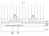
도 1은 본 발명의 일 실시예에 따른 유기발광 표시 장치의 단면도이다.
도 2 내지 도 28은 본 발명의 일 실시예에 따른 유기발광 표시장치의 제조 방법을 개략적으로 나타낸 단면도이다.
도 29 내지 도 32는 본 발명의 다른 실시예에 따른 유기 발광 표시 장치의 제조 방법을 개략적으로 나타낸 단면도이다.1 is a cross-sectional view of an organic light emitting display device according to an exemplary embodiment of the present invention.
2 to 28 are cross-sectional views schematically illustrating a method of manufacturing an organic light emitting display device according to an embodiment of the present invention.
29 to 32 are cross-sectional views schematically illustrating a method of manufacturing an organic light emitting display device according to another exemplary embodiment of the present invention.
본 발명의 이점 및 특징, 그리고 그것들을 달성하는 방법은 첨부되는 도면과 함께 상세하게 후술되어 있는 실시예들을 참조하면 명확해질 것이다. 그러나 본 발명은 이하에서 개시되는 실시예들에 한정되는 것이 아니라 서로 다른 다양한 형태로 구현될 것이며, 단지 본 실시예들은 본 발명의 개시가 완전하도록 하며, 본 발명이 속하는 기술분야에서 통상의 지식을 가진 자에게 발명의 범주를 완전하게 알려주기 위해 제공되는 것이며, 본 발명은 청구항의 범주에 의해 정의될 뿐이다. Advantages and features of the present invention, and methods for achieving them will become apparent with reference to the embodiments described below in detail in conjunction with the accompanying drawings. However, the present invention is not limited to the embodiments disclosed below, but will be implemented in various forms, and only the present embodiments are intended to complete the disclosure of the present invention, and the general knowledge in the art to which the present invention pertains. It is provided to fully convey the scope of the invention to those skilled in the art, and the present invention is defined only by the scope of the claims.
소자(elements) 또는 층이 다른 소자 또는 층의 "상(on)"으로 지칭되는 것은 다른 소자 바로 위에 또는 중간에 다른 층 또는 다른 소자를 개재한 경우를 모두 포함한다. 명세서 전체에 걸쳐 동일 참조 부호는 동일 구성 요소를 지칭한다.References to elements or layers as "on" of another element or layer include all instances where another layer or other element is interposed over or in the middle of another element. Like reference numerals refer to like elements throughout.
비록 제1, 제2 등이 다양한 구성요소들을 서술하기 위해서 사용되나, 이들 구성요소들은 이들 용어에 의해 제한되지 않음은 물론이다. 이들 용어들은 단지 하나의 구성요소를 다른 구성요소와 구별하기 위하여 사용하는 것이다. 따라서, 이하에서 언급되는 제1 구성요소는 본 발명의 기술적 사상 내에서 제2 구성요소일 수도 있음은 물론이다.Although the first, second, etc. are used to describe various components, these components are of course not limited by these terms. These terms are only used to distinguish one component from another. Therefore, of course, the first component mentioned below may be a second component within the technical spirit of the present invention.
이하, 첨부된 도면을 참조하여 본 발명의 실시예들에 대하여 설명한다. 도 1은 본 발명의 일 실시예에 따른 유기발광 표시 장치의 단면도이다.Hereinafter, with reference to the accompanying drawings will be described embodiments of the present invention. 1 is a cross-sectional view of an organic light emitting display device according to an exemplary embodiment of the present invention.
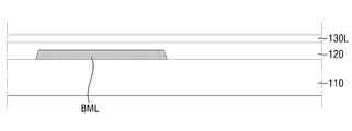
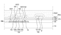
도 1을 참조하면, 본 발명의 일 실시예에 따른 유기 발광 표시 장치(100)는 기판(110) 상에 배치된 버퍼층(120), 버퍼층 상에 배치된 박막 트랜지스터(TR), 버퍼층 하부에 박막 트랜지스터에 대응하여 형성된 하부 전극패턴(BML), 박막 트랜지스터(TR) 상부에 배치된 화소 전극(181)을 포함할 수 있다.Referring to FIG. 1, the organic light
기판(110)은 유리와 같은 투명 기판, 석영, 세라믹, 실리콘 기판, 플라스틱 등의 플렉시블 기판 등 당업자의 필요에 따라 적절히 선택할 수 있다.The
기판(110)은 그 위에 박막 트랜지스터(TR)가 형성되는 영역인 박막 트랜지스터 영역(TRA)과 그 위에 커패시터가 형성되는 영역인 커패시터 영역(SA)을 포함할 수 있다.The
기판(110) 상에는 하부 전극패턴(BML)이 배치된다. 하부 전극패턴(BML)은 기판(110)의 박막 트랜지스터 영역(TRA) 상에 배치될 수 있다. 하부 전극패턴(BML)은 박막 트랜지스터(TR)의 반도체층(130)과 중첩하도록 배치되어 반도체층(130)으로 광이 입사하는 것을 방지하는 한편, 박막 트랜지스터(TR)의 제1 전극(191)과 전기적으로 연결되어 해당 전압을 인가받음으로써, 주변의 전극으로부터 박막 트랜지스터(TR)가 영향을 받는 것을 차폐할 수 있다. The lower electrode pattern BML is disposed on the
하부 전극패턴(BML)은 Ag, Mg, Al, Pt, Pd, Au, Ni, Nd, Ir, Cr, Li,Ca, Mo, Ti, W, MoW 및 Cu 가운데 선택된 하나 이상의 물질로 형성될 수 있으나, 이에 제한되는 것은 아니다.The lower electrode pattern BML may be formed of one or more materials selected from Ag, Mg, Al, Pt, Pd, Au, Ni, Nd, Ir, Cr, Li, Ca, Mo, Ti, W, MoW, and Cu. However, the present invention is not limited thereto.
하부 전극패턴(BML)이 배치된 기판(110)의 상부에는 버퍼층(120)이 배치될 수 있다. 버퍼층(120)은 기판(110)의 전면 상에 배치되어 하부 전극패턴(BML)을 덮을 수 있다. 버퍼층(120)은 기판(110)에서 유출되는 알칼리 이온 등 불순물의 침투로부터 후속 공정으로 형성되는 박막 트랜지스터(TR)를 보호하고 표면을 평탄화하는 역할을 할 수 있다. The
버퍼층(120) 상부의 박막 트랜지스터 영역(TRA)에는 박막 트랜지스터(TR)가 배치될 수 있다. 박막 트랜지스터(TR)는 버퍼층(120) 상에 순차적으로 적층된 반도체층(130), 게이트 절연막(150) 및 게이트 전극(160) 그리고 반도체층(130)과 연결되는 제1 전극(191)과 제2 전극(192)을 포함할 수 있다. 제1 전극(191)과 제2 전극(192) 중 어느 하나는 소스 전극이고, 다른 하나는 드레인 전극일 수 있다. The thin film transistor TR may be disposed in the thin film transistor region TRA on the
반도체층(130)은 산화물 반도체를 포함할 수 있다. 반도체층(130)은 예를 들어, 인듐-갈륨-아연-산화물(IGZO), 인듐-아연-산화물(a-IZO), 인듐-주석-아연-산화물(ITZO) 및 인듐-갈륨-산화물(IGO) 등으로부터 선택된 어느 한 화합물을 이용하여 형성될 수 있으나, 이에 한정되는 것은 아니다.The
이러한 산화물로 이루어진 반도체층(1130)은 비교적 저온에서 형성가능하고, 플라스틱판이나 필름 등의 기판 위에 박막을 형성하는 것이 가능하며, 비정질 실리콘보다 전자 이동속도가 10배 이상 빨라 최근 UD(Ultra Definition) 이상의 고해상도 및 240Hz이상의 고속구동에 적합한 이점이 있다. The semiconductor layer 1130 made of such an oxide can be formed at a relatively low temperature, and a thin film can be formed on a substrate such as a plastic plate or a film, and the electron transfer speed is 10 times faster than that of amorphous silicon. There is an advantage that is suitable for high resolution of more than 240Hz and high speed drive.
반도체층(130)은 채널 영역(130b)과 그 양측에 배치된 제1 영역(130a) 및 제2 영역(130c)을 포함할 수 있다. 채널 영역(130b)은 상부의 게이트 전극(160)과 중첩할 수 있다. 제1 영역(130a)은 제1 전극(191)과 전기적으로 연결되고, 제2 영역(130c)은 제2 전극(192)과 전기적으로 연결될 수 있다. 제1 영역(130a)은 제1 소스/드레인 영역이고 제2 영역(130c)은 제2 소스/드레인 영역일 수 있다. 제1 전극(191)이 소스 전극이고 제2 전극(192)이 드레인 전극일 경우, 제1 영역(130a)은 소스 영역이 되고 제2 영역(130c)은 드레인 영역이 될 수 있다. 제1 영역 및 제2 영역(130a, 130c)은 금속화 공정을 통해 금속화되어 있을 수 있지만, 이에 제한되는 것은 아니다. The
게이트 절연막(150)은 반도체층(130) 상에 형성될 수 있다. 게이트 절연막(150)의 너비는 반도체층(130)의 채널 영역(130b)의 너비와 실질적으로 동일하거나 그보다는 좁고, 게이트 전극(160)의 너비와 실질적으로 동일하거나 그보다 넓게 형성될 수 있다. 게이트 절연막(150)의 너비를 위와 같은 범위 내에서 조절하면, 별도의 마스크 공정 없이 게이트 절연막(150)을 이용하여 반도체층(130)의 금속화 공정을 진행할 수 있는 이점이 있다, The
게이트 절연막(150)은 실리콘 옥사이드(SiO2), 실리콘 나이트라이드(SiNx) 및 실리콘 옥시나이트라이드(SiON) 등으로 이루어질 수 있으나, 이에 한정되는 것은 아니다. The
게이트 전극(160)은 게이트 절연막(150) 상에 게이트 절연막(150)과 실질적으로 동일하거나 그보다 좁은 너비로 배치될 수 있다. 그리고, 게이트 전극(160)은 반도체층(130)의 채널 영역(130b)과 중첩될 수 있다. 게이트 전극(160)은 몰리브덴(Mo), 텅스텐(W), 알루미늄 네오디뮴(AlNd), 티타늄(Ti), 알루미늄(Al), 은(Ag) 및 이들의 합금으로 이루어진 군에서 선택된 단독 또는 이들의 혼합물로 단일층을 형성하거나 배선 저항을 줄이기 위해 저저항 물질인 Mo, Al 또는 Ag의 이중층 또는 다중층 구조로 형성할 수도 있다. 즉, 배선 저항을 줄이기 위해 다중층의 도전막을 순차적으로 적층하여 형성할 수 있으며, 구체적으로, Mo/Al/Mo, MoW/AlNd/MoW, Mo/Ag/Mo, Mo/Ag합금/Mo 또는 Ti/Al/Mo 로 이루어진 다중층 구조를 취할 수도 있다.The
버퍼층(120) 상부의 커패시터 영역(SA)에는 게이트 절연막(150)과 동일한 물질로 이루어진 절연패턴(IP)이 형성되고, 절연패턴(IP) 상부에는 게이트 전극(160)과 동일한 물질로 이루어진 제1 커패시터 전극(141)이 배치될 수 있다. An insulating pattern IP made of the same material as the
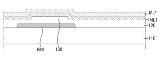
게이트 전극(160) 및 제1 커패시터 전극(141)이 형성된 기판(110) 전면에 층간 절연막(170)이 배치될 수 있다. An interlayer insulating
층간 절연막(170)은 기판(110)의 전면 상에 게이트 전극(160) 및 제1 커패시터 전극(141)을 덮도록 소정의 두께로 형성될 수 있다. 층간 절연막(170)은 게이트 전극(160)과 제1 및 제2 전극(191, 192)을 절연시키는 역할을 하고, 제2 커패시터 전극(142)과 제1 캐패시터 전극(141) 사이에 배치되어 유전막 역할을 할 수 있다.The interlayer insulating
층간 절연막(170)은 2층 이상의 다중층으로 형성될 수 있으며, 층간 절연막(170)이 제1 층간 절연막(171) 및 제2 층간 절연막(172)의 이중층으로 형성된 경우를 일례로 설명한다. The interlayer insulating
제1 층간 절연막(170a) 및 제2 층간 절연막(170b)은 각각 무기 절연막으로 형성될 수 있다. 예를 들어, 제1 층간 절연막(170a) 및 제2 층간 절연막(170b)은 각각 SiO2, SiNx, SiON, Al2O3, TiO2, Ta2O5, HfO2, ZrO2, BST 또는 PZT 등으로 이루어질 수 있으나, 이에 한정되는 것은 아니다. The first
제1 층간 절연막(170a) 및 제2 층간 절연막(170b)은 동일한 물질로 이루어질 수도 있지만, 서로 다른 물질을 포함하여 이루어질 수도 있다. 이하에서는 제1 층간 절연막(170a)이 실리콘 옥사이드(SiO2)로 이루어지고, 제2 층간 절연막(170b)이 실리콘 나이트라이드(SiNx)로 이루어진 경우를 일례로 설명한다. The first
층간 절연막(170) 상의 박막 트랜지스터 영역(TRA)에는 박막 트랜지스터(TR)의 제1 및 제2 전극(191, 192)이 배치될 수 있고, 층간 절연막(170) 상의 커패시터 영역(CA)에는 제1 및 제2 전극(191, 192)과 동일한 물질로 이루어진 제2 커패시터 전극(142)이 배치될 수 있다.First and
제1 및 제2 전극(191, 192)과 제2 커패시터 전극(142)은 알루미늄, 티타늄, 네오디뮴, 알루미늄, 은, 몰리브덴, 텅스텐, 몰리브덴, 텅스텐 및 이들의 합금으로 이루어진 군에서 선택된 단독 또는 이들의 혼합물로 단일층을 형성하거나 이중층 또는 다중층 구조로 형성할 수 있다. 예를 들어, 제1 및 제2 전극(191, 192)과 제2 커패시터 전극(142)은 Ti/Al/Ti, Mo/Al/Mo, MoW/AlNd/MoW, Mo/Ag/Mo, Mo/Ag합금/Mo 또는 Ti/Al/Mo 등이 순차적으로 적층된 구조를 취할 수도 있다.The first and
상술한 바와 같이 제1 및 제2 전극(191, 192)은 반도체층(130)의 제1 및 제2 영역(130a, 130c)과 전기적으로 연결된다. 즉, 층간 절연막(170)은 제1 및 제2 영역(130a, 130c) 각각에 대응하여 형성된 제2 컨택홀(CNT2)을 포함할 수 있으며, 제2 컨택홀(CNT2)을 통하여 제1 및 제2 전극(191, 192)은 반도체층(130)의 제1 및 제2 영역(130a, 130c)과 각각 연결될 수 있다.As described above, the first and
또한, 제1 및 제2 전극(191, 192) 중 하나는 버퍼층(120) 하부에 배치된 하부 전극패턴(BML)과 연결될 수 있다. 즉, 층간 절연막 (170) 및 버퍼층(120)은 하부 전극패턴(BML)을 노출시키는 제1 컨택홀(CNT1)을 포함할 수 있으며, 제1 및 제2 전극(191, 192) 중 하나는 제1 컨택홀(CNT1)을 통하여 하부 전극패턴(BML)과 연결되어 하부 전극패턴(BML)이 다른 전극에 영향을 미치는 것을 방지할 수 있게 한다. 제1 전극(191)이 하부 전극패턴(BML)과 연결되는 것을 일례로 설명하면, 제1 전극(191)은 제1 컨택홀(CNT1)을 통하여 하부 전극패턴(BML)과 연결되고 제2 컨택홀(CNT2)을 통하여 제1 영역(130a)과 연결될 수 있게 된다. In addition, one of the first and
층간 절연막(170) 상에는 패시베이션층(PAS)이 배치될 수 있다. 패시베이션층(PAS)은 순차 적층된 제1 패시베이션층(PAS1)과 제2 패시베이션층(PAS2)을 포함할 수 있다. The passivation layer PAS may be disposed on the
제1, 제2 패시베이션층(PAS1, PAS2)은 각각 유기막 또는 무기막으로 이루어질 수 있다. 제1 패시베이션층(PAS1)은 무기막으로 이루어지고, 제2 패시베이션층(PAS2)은 유기막으로 이루어진 경우를 일례로 설명하면, 제1 패시베이션층(PAS1)은 SiO2, SiNx, SiON, Al2O3, TiO2, Ta2O5, HfO2, ZrO2, BST, PZT 등의 무기막으로 이루어질 수 있으며, 제2 패시베이션층(PAS2)은 일반 범용고분자(PMMA, PS), phenol 그룹을 갖는 고분자 유도체, 아크릴계 고분자, 이미드계 고분자, 아릴에 테르계 고분자, 아미드계 고분자, 불소계 고분자, p-자일렌계 고분자, 비닐알콜계 고분자 및 이들의 블렌드 등의 유기막으로 이루어질 수 있으나, 이에 한정되는 것은 아니다.The first and second passivation layers PAS1 and PAS2 may be formed of organic layers or inorganic layers, respectively. Referring to the case where the first passivation layer (PAS1) is made of an inorganic film, the second passivation layer (PAS2) is made of an organic film as an example, the first passivation layer (PAS1) is SiO2, SiNx, SiON, Al2O3, TiO2 , Ta2O5, HfO2, ZrO2, BST, PZT, etc., the second passivation layer (PAS2) is a general purpose polymer (PMMA, PS), a polymer derivative having a phenol group, acrylic polymer, imide polymer, An aryl ether polymer, an amide polymer, a fluorine polymer, a p-xylene polymer, a vinyl alcohol polymer and blends thereof may be formed of organic membranes, but is not limited thereto.
패시베이션층(PAS)은 층간 절연막(170) 상부를 평탄화할 수 있으며, 상부에는 화소 전극(181)이 배치될 수 있다. 화소 전극(181)은 인듐-주석-산화물(Indium-Tin-Oxide: ITO), 인듐-아연-산화물(Indium-Zinc-Oxide: IZO), 산화아연(Zinc Oxide: ZnO), 산화인듐(Induim Oxide: In2O3)의 일함수가 높은 물질층과 은(Ag), 마그네슘(Mg), 알루미늄(Al), 백금(Pt), 납(Pd), 금(Au), 니켈(Ni), 네오듐(Nd), 이리듐(Ir), 크롬(Cr), 리튬(Li), 칼슘(Ca) 또는 이들의 혼합물 등과 같은 반사성 물질층이 적층된 적층막 구조를 가질 수 있다. 화소 전극(181)은 ITO/Mg, ITO/MgF, ITO/Ag, ITO/Ag/ITO의 복수층 구조를 가질 수 있으나, 이에 한정되는 것은 아니다. The passivation layer PAS may planarize the upper portion of the interlayer insulating
화소 전극(181)은 발광 다이오드의 전공 주입 전극인 애노드 전극이 될 수 있다. The
화소 전극(181)은 제1 전극(191) 또는 제2 전극(192) 중 어느 하나와 연결될 수 있다. 화소 전극(181)이 제1 전극(191)과 연결된 경우를 일례로 설명하면, 제1, 2 패시베이션층(PAS1, PAS2)은 제3 컨택홀(CNT3)을 포함할 수 있으며, 제3 컨택홀(CNT3)을 통하여 화소 전극(181)과 제1 전극(191)이 연결될 수 있다. The
패시베이션층(PAS) 상부에 화소 전극(181)을 노출시키는 화소정의막(182)(Pixel Difined Layer)이 배치될 수 있다. 즉, 패시베이션층(PAS) 상부에 화소 전극(181)의 가장자리를 둘러싸는 형태로 화소 정의막(182)이 배치될 수 있다. 화소 정의막(182)은 폴리아크릴계 수지, 에폭시 수지, 페놀 수지, 폴리아미드계 수지, 폴리이미드계 수지, 불포화 폴리에스테르계 수지, 폴리페닐렌계 수지, 폴리페닐렌설파이드계 수지 및 벤조사이클로부텐으로 이루어 진 군으로부터 선택된 단독 또는 이들의 혼합물로 형성될 수 있다.A pixel defined
도면으로 도시하지는 않았지만, 화소 정의막(182)에 의해 노출된 화소 전극(181) 상에는 유기 발광층(미도시) 및 전자 주입 전극으로서 공통 전극인 캐소드 전극(미도시)이 배치될 수 있다. 이와 같은 구조에 의해 전공과 전자가 유기 발광층 내부로 주입되고 주입된 전공과 전자가 결합한 엑시톤(exiton)이 여기상태로부터 기저상태로 떨어질때 발광이 이루어질 수 있다.Although not illustrated in the drawing, an organic emission layer (not shown) and a cathode electrode (not shown), which is a common electrode, may be disposed on the
이하, 상술한 유기발광 표시 장치의 제조 방법에 대해 설명한다. Hereinafter, the method of manufacturing the organic light emitting display device described above will be described.
도 2 내지 도 28은 본 발명의 일 실시예에 따른 유기발광 표시장치의 제조 방법을 공정순서에 따라 순차적으로 나타낸 단면도들이다. 도 1과 실질적으로 동일한 구성요소에 대해서는 동일한 부호로 나타내고 자세한 설명을 생략한다.2 to 28 are cross-sectional views sequentially illustrating a method of manufacturing an organic light emitting display device according to an embodiment of the present invention according to a process sequence. Components substantially the same as in Fig. 1 are denoted by the same reference numerals and detailed description thereof will be omitted.
도 2를 참조하면, 기판(110) 상에 하부 전극패턴 물질층(BMLL)을 형성하고, 제1 마스크(M1)를 통하여 제 1 감광막 패턴(PR1)을 형성한다. Referring to FIG. 2, a lower electrode pattern material layer BMLL is formed on the
설명의 편의를 위하여 감광막이 포지티브(positive) 감광막인 경우를 설명하나, 본 발명은 이에 한정되지 않으며 감광막으로 네거티브(negative) 감광막이 사용될 수도 있다.For convenience of description, a case in which the photoresist film is a positive photoresist film will be described. However, the present invention is not limited thereto, and a negative photoresist film may be used as the photoresist film.
제1 마스크(M1)는 광투과부(TA) 및 광차단부(PA)를 포함할 수 있다. 광투과부(TA)는 조사되는 광을 투과시키고, 광차단부(PA)는 조사되는 광을 차단시킬 수 있다. 제1 마스크(MA1)의 광차단부(PA)가 하부 전극패턴(BML)이 형성될 영역에 대응하도록 배치된다. 이어, 제1 마스크(MA1)를 통하여 감광막에 광을 조사한 후 감광막을 현상하면 광투과부(TA)에 대응하는 감광막 영역이 제거되고 광차단부(PA)에 대응하는 감광막 영역이 남아서 제1 감광막 패턴(PR1)이 형성된다.The first mask M1 may include a light transmitting part TA and a light blocking part PA. The light transmitting part TA may transmit light to be irradiated, and the light blocking part PA may block light to be irradiated. The light blocking part PA of the first mask MA1 is disposed to correspond to the region where the lower electrode pattern BML is to be formed. Subsequently, when the photoresist film is irradiated with light through the first mask MA1 and the photoresist film is developed, the photoresist area corresponding to the light transmission part TA is removed and the photoresist area corresponding to the light shielding part PA remains to leave the first photoresist pattern. PR1 is formed.
도 3 및 도 4를 참조하면, 제1 감광막 패턴(PR1)을 식각 마스크로 하여 하부 전극패턴 물질층(BMLL)을 식각한 후, 상기 제1 감광막 패턴(PR1)을 제거하여 하부 전극패턴(BML)을 형성할 수 있다. 제1 감광막 패턴(PR1)을 제거하는 방법은 산소를 사용하는 애싱(ashing) 공정 등이 이용될 수 있으나, 이에 제한되는 것은 아니다3 and 4, after etching the lower electrode pattern material layer BMLL using the first photoresist pattern PR1 as an etching mask, the first photoresist pattern PR1 is removed to remove the lower electrode pattern BML. ) Can be formed. The ashing process using oxygen may be used as the method of removing the first photoresist layer pattern PR1, but is not limited thereto.
도 5를 참조하면, 하부 전극패턴(BML)이 형성된 기판(110) 상에 버퍼층(120)을 형성한다.Referring to FIG. 5, the
버퍼층(120)은 화학 기상 증착 또는 플라즈마 화학 기상 증착(Plasma Enhanced Chemical Vapor Deposition)등으로 형성될 수 있다. 버퍼층(120)은 실리콘 옥사이드(SiO2)로 형성될 수 있으나, 이에 한정되는 것은 아니다.The
도 6을 참조하면, 버퍼층(120) 상부에 반도체 물질층(130L)을 형성한다.Referring to FIG. 6, a
반도체 물질층(130L)은 기상 성막법 및 포토리소그래피법을 이용하여 형성할 수 있다. 예를 들면, 기상 성막법으로 IGZO 등으로 이루어진 반도체 물질층(130L)을 형성할 수 있으며, 기상 성막법 중에서 스퍼터링법 및 펄스 레이저 증착법 (PLD 법)을 이용할 수 있으나, 이에 한정되는 것은 아니다. The
도 7을 참조하면, 제2 마스크(M2)를 통하여 제2 감광막 패턴(PR2)을 형성한다. 제2 마스크(M2)는 광투과부(TA) 및 광차단부(PA)를 포함할 수 있으며, 제2 마스크(MA2)의 광차단부(PA)가 반도체층(130)이 형성될 영역에 대응하도록 배치한다. 이어, 제2 마스크(MA2)를 통하여 감광막에 광을 조사한 후 감광막을 현상하면 광투과부(TA)에 대응하는 감광막 영역이 제거되고 광차단부(PA)에 대응하는 감광막 영역이 남아서 제2 감광막 패턴(PR2)이 형성된다.Referring to FIG. 7, a second photosensitive film pattern PR2 is formed through the second mask M2. The second mask M2 may include a light transmitting part TA and a light blocking part PA, and the light blocking part PA of the second mask MA2 corresponds to a region where the
도 8 및 도 9를 참조하면, 제2 감광막 패턴(PR2)을 식각 마스크로 하여 반도체 물질층(130L)을 식각한 후, 상기 제2 감광막 패턴(PR2)을 제거하여 반도체층(130)을 형성한다.8 and 9, after etching the
도 10을 참조하면, 반도체층(130)이 형성된 버퍼층(120) 상부에 제1 절연물질층(IML1)을 형성한다. 제1 절연물질층(IML1)은 SiNx, SiO2, SiON 등의 무기물을 이용하여 화학 기상 증착으로 형성할 수 있으나, 이에 한정되는 것은 아니고, 무기물과 유기물의 복합체로 형성될 수도 있다.Referring to FIG. 10, a first insulating material layer IML1 is formed on the
도 11을 참조하면, 제1 절연물질층(IML1) 상에 제1 금속물질층(ML1)을 스퍼터링(sputtering) 등의 방법으로 형성한다. Referring to FIG. 11, the first metal material layer ML1 is formed on the first insulating material layer IML1 by sputtering or the like.
도 12를 참조하면, 제3 마스크(M3)를 통하여 제3 감광막 패턴(PR3)을 형성한다. 제3 마스크(M3)는 광투과부(TA) 및 광차단부(PA)를 포함할 수 있으며, 제3 마스크(MA3)의 광차단부(PA)가 게이트 전극(160) 및 제1 커패시터 전극(141)이 형성될 영역에 대응하도록 배치한다. 이어, 제3 마스크(MA3)를 통하여 감광막에 광을 조사한 후 감광막을 현상하면 광투과부(TA)에 대응하는 감광막 영역이 제거되고 광차단부(PA)에 대응하는 감광막 영역이 남아서 제3 감광막 패턴(PR3)이 형성된다.Referring to FIG. 12, a third photoresist pattern PR3 is formed through the third mask M3. The third mask M3 may include a light transmitting part TA and a light blocking part PA, and the light blocking part PA of the third mask MA3 includes the
도 13 및 도 14를 참조하면, 제3 감광막 패턴(PR3)을 식각 마스크로 하여 제1 금속물질층(ML1) 및 제1 절연물질층(IML1)을 식각한 후, 상기 제3 감광막 패턴(PR3)을 제거하여 게이트 절연막(150)과 게이트 절연막(150) 상부의 게이트 전극(160) 및 절연패턴(IP)과 절연패턴(IP) 상부에 제1 커패시터 전극(141)을 형성할 수 있다.Referring to FIGS. 13 and 14, after etching the first metal material layer ML1 and the first insulating material layer IML1 using the third photoresist pattern PR3 as an etching mask, the third photoresist pattern PR3 is formed. ) May be removed to form the
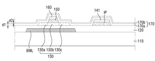
도 15를 참조하면, 게이트 절연막(150)을 마스크로 반도체층(130)의 금속화 공정을 진행하여 반도체층(130)의 제1 영역(130a)과 제2 영역(130c)을 형성할 수 있다. 이하, 제1 영역(130a)은 소스 영역이고, 제2 영역(130c)은 드레인 영역을 경우를 일례로 설명한다. 이에 따라, 반도체층(130)은 소스 영역(130a), 채널 영역(130b) 및 드레인 영역(130c)로 구분될 수 있게 된다.Referring to FIG. 15, the metallization process of the
도 16을 참조하면, 게이트 전극(160) 및 제1 커패시터 전극(141)이 형성된 버퍼층(120) 상부로 제1 층간 절연막(170a)과 제2 층간 절연막(170b)이 순차적으로 형성될 수 있다. 구체적으로, 제1 층간 절연막(170a)의 두께가 제2 층간 절연막(170a)의 두께보다 두껍게 형성될 수 있다. 예를 들어 제1 층간 절연막(170a)의 두께(d1)는 3000Å일 수 있으며, 제2 층간 절연막(170b)의 두께(d2)는 2000Å일 수 있다. Referring to FIG. 16, a first
식각시 사용되는 혼합가스에 대하여 제1 층간 절연막(170a)의 에칭 레이트(etching rate)가 제2 층간 절연막(170a)의 에칭 레이트(etching rate)보다 작은 물질로 이루어질 수 있다. The etching rate of the first
제1 층간 절연막(170a) 및 제2 층간 절연막(170b)은 무기 절연막으로 형성될 수 있다. 예를 들어, SiO2, SiNx, SiON, Al2O3, TiO2, Ta2O5, HfO2, ZrO2, BST 또는 PZT 등으로 이루어질 수 있으나, 이에 한정되는 것은 아니다.The first
산화물 반도체의 동작 불안정성을 야기시키는 원인은 여러 가지가 있으며 그 중 제1 층간 절연막(170a)의 특성은 무엇보다도 중요한 요인으로 작용한다. 특히 산화물 반도체의 전기적 특성이 쉘로우 도너(shallow donor)인 수소(H)의 도핑 정도에 따라 크게 변하는 것을 고려할 때, 제1 층간 절연막(170a) 내에 포함된 수소의 양에 따라 산화물 반도체의 특성이 변화 될 수 있다. 일반적으로 실리콘 나이트라이드(SiNx)가 실리콘 옥사이드(SiO2)보다 더 많은 수소를 포함하는데, 실리콘 나이트라이드(SiNx)를 절연막으로 사용할 때 실리콘 옥사이드(SiO2)를 사용하는 경우에 비해 바이어스 스트레스(bias stress) 특성이 더 좋지 않다. 이는 인터페이스에 존재하는 수소와 관련된 결함에 의한 것으로 해석될 수 있다. 따라서, 제1 층간 절연막(170a)을 실리콘 옥사이드(SiO2)로 형성하고, 제2 층간 절연막(170b)을 실리콘 나이트라이드(SiNx)로 형성하는 것이 바람직하다.There are many causes of the operation instability of the oxide semiconductor, among which the characteristics of the first
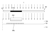
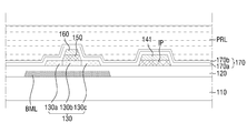
도 17 및 도 18을 참조하면, 제2 층간 절연막(170b) 상부에 감광막 물질층(PRL)을 도포하고, 제4 마스크(M4)를 통하여 제4 감광막 패턴(PR4)을 형성한다.17 and 18, the photoresist material layer PRL is coated on the second
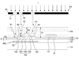
제4 마스크(M4)는 하프톤 마스크 또는 슬릿 마스크일 수 있으며, 광을 투과시키는 광투과부(TA), 광을 차단하는 광차단부(PA), 광을 부분적으로 투과시키는 반투과부(HA)를 포함할 수 있다. 광투과부(TA)가 제1 컨택홀(CNT1)이 형성될 영역에 대응하고 반투과부(HA)는 제2 컨택홀(CNT2)이 형성될 영역에 대응하도록 제4 마스크(MA4)를 배치하고, 제4 마스크(MA4)를 통하여 감광막에 광을 조사한 후(노광), 감광막을 현상(develop)하면 광투과부(TA) 및 반투과부(HA)에 대응하는 감광막 영역이 서로 다른 두께로 제거되고, 광차단부(PA)에 대응하는 감광막 영역이 남게 된다. The fourth mask M4 may be a halftone mask or a slit mask, and includes a light transmitting part TA for transmitting light, a light blocking part PA for blocking light, and a semi-transmitting part HA for partially transmitting light. It may include. The light transmissive part TA corresponds to the area where the first contact hole CNT1 is to be formed, and the transflective part HA arranges the fourth mask MA4 to correspond to the area where the second contact hole CNT2 is to be formed, After irradiating light to the photoresist film through the fourth mask MA4 (exposure), developing the photoresist film removes the photoresist areas corresponding to the light transmissive part TA and the transflective part HA to different thicknesses. The photoresist area corresponding to the blocking part PA remains.
구체적으로, 광투과부(TA)에 대응되는 영역에는 제1 홀(H1)이 형성되고, 반투과부(HA)에 대응되는 영역에는 제1 홀(H1)보다 깊이가 낮은 제2 홀(H2) 및 제3 홀(H3)이 형성된다. 즉, 제4 감광막 패턴(PR4)은 제1 컨택홀(CNT1)이 형성될 영역에 대응하는 제2 층간 절연막(170b)을 노출하는 제1 홀(H1)이 형성되고, 제2 컨택홀(CNT2)이 형성될 영역에 각각 대응하여 제2 층간 절연막(170b) 상부에 잔여 감광물(RP)이 배치된 제2, 제3 홀(H2, H3)이 형성될 수 있다.In detail, a first hole H1 is formed in an area corresponding to the light transmitting part TA, and a second hole H2 having a depth lower than that of the first hole H1 is formed in an area corresponding to the transflective part HA, and The third hole H3 is formed. That is, in the fourth photoresist pattern PR4, the first hole H1 exposing the second
예시적인 실시예에서 광차단부 (PA)에 대응하는 제4 감광막 패턴(PR4)의 두께(D1)는 24000Å일 수 있으며, 잔여 감광물(RP)의 두께(D2)는 7000Å일 수 있고, 제1 홀(H1)의 깊이는 24000Å 일 수 있으며, 제2 홀(H2) 및 제3 홀(H3)의 각각의 깊이는 17000Å일 수 있고, 게이트 전극(160)에 대응되는 제2 층간 절역막(170b) 상에 형성되는 제4 감광막 패턴(PR4)의 두께(D3)는 17000Å일 수 있다. 다만, 이에 한정되는 것은 아니며, 제1, 제2 층간 절연막(170a, 170b) 및 버퍼층(120)의 물질, 두께, 에칭시 사용되는 혼합가스 등에 따라 다양하게 변형될 수 있다.In an exemplary embodiment, the thickness D1 of the fourth photoresist pattern PR4 corresponding to the light blocking part PA may be 24000 μs, and the thickness D2 of the remaining photosensitive material RP may be 7000 μs, The depth of the first hole H1 may be 24000 μm, the depth of each of the second hole H2 and the third hole H3 may be 17000 μm, and a second interlayer blocking film corresponding to the
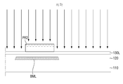
도 19 및 도 20을 참조하면, 이어, 상기 결과물을 식각한다. 즉, 제4 감광막 패턴(PR4)이 형성된 구조물에 대해 예컨대 건식 식각을 진행할 수 있다. 본 단계는 제4 감광막 패턴(PR4)이 노출하는 부분에 대한 식각 뿐만 아니라 제4 감광막 패턴(PR4) 자체의 식각도 포함한다. 구체적으로 설명하면, 식각 가스에 의하여 제1 홀(H1)에 의하여 노출된 제2 층간 절연막(170b), 제1 층간 절연막(170a) 및 버퍼층(120)을 식각 동안에, 제2 홀(H2)에 의하여 노출된 잔여 감광물(RP), 제2 층간 절연막(170b), 제1 층간 절연막(170a)이 식각된다. 따라서, 잔여 감광물(RP)은 제1 컨택홀(CNT1)이 형성되는 동안 산화물 반도체층이 노출되는 시간을 지연시킬 수 있게 한다. 19 and 20, the resultant is etched. That is, for example, dry etching may be performed on the structure on which the fourth photoresist pattern PR4 is formed. This step includes not only the etching of the portion exposed by the fourth photoresist pattern PR4, but also the etching of the fourth photoresist pattern PR4 itself. Specifically, the second
그 다음으로, 식각되고 남은 제4 감광막 패턴(PR4)을 제거하여, 하부 전극패턴(BML)을 노출하는 제1 컨택홀(CNT1)과 소스 영역(130a) 및 드레인 영역(130c)을 각각 노출하는 제2 컨택홀(CNT2)을 형성할 수 있다.Next, the fourth photoresist pattern PR4 remaining after etching is removed to expose the first contact hole CNT1 exposing the lower electrode pattern BML, the
제1 층간 절연막(170a)의 두께(d1)가 제2 층간 절연막(170a)의 두께(d2)보다 두껍게 형성될 수 있으며, 버퍼층(120)이 두께(d3)는 잔여 감광물(RP)의 두께(D2)보다 얇게 형성될 수 있다. 예시적인 실시예에서, 잔여 감광물(RP)의 두께(D2)는 7000Å인 경우, 버퍼층(120)의 두께(d3)는 7000Å이하로 형성될 수 있다. The thickness d1 of the first
그리고, 식각시 사용되는 혼합가스에 대하여 제2 층간 절연막(170a)의 에칭 레이트(etching rate)는 제1 층간 절연막(170a) 및 버퍼층(120)의 에칭 레이트(etching rate)보다 클 수 있다. In addition, an etching rate of the second
제1 층간 절연막(170a)의 에칭 레이트(etching rate)와 버퍼층(120)의 에칭 레이트(etching rate)는 동일할 수 있다. An etching rate of the first
잔여 감광물(RP)의 에칭 레이트(etching rate)는 제2 층간 절연막(170a)의 에칭 레이트(etching rate)보다 작고, 제1 층간 절연막(170a) 및 버퍼층(120)의 에칭 레이트(etching rate)보다 클 수 있다.The etching rate of the remaining photosensitive material RP is smaller than the etching rate of the second
예시적인 실시예에서, 제2 층간 절연막(170a)은 실리콘 나이트라이드(SiNx)로 이루어지고, 제1 층간 절연막(170a) 및 버퍼층(120)은 실리콘 옥사이드(SiO2)로 이루어지며, 소스 및 드레인 영역(130a, 130b)은 IGZO로 이루어 질 수 있으며, 삼불화질소(NF3) 및 산소(O2)의 혼합가스를 이용하여 식각을 진행하는 경우 제2 층간 절연막(170a)의 에칭 레이트(etching rate)는 4425Å/min일 수 있으며, 제1 층간 절연막(170a) 및 버퍼층(120) 에칭 레이트(etching rate)는 2185Å/min일 수 있고, 잔여 감광물(RP)의 에칭 레이트(etching rate)는 3825Å/min일 수 있으며, 소스 및 드레인 영역(130a, 130b)을 이루는 IGZO의 에칭 레이트(etching rate)는 190Å/min일 수 있다.In an exemplary embodiment, the second
따라서, 제1 컨택홀(CNT1)과 제2 컨택홀(CNT2)을 하나의 마스크로 동시에 형성하는 경우에도 제1 컨택홀(CNT1)을 형성하기 위하여 제1, 제2 층간 절연막(170a, 170b) 및 버퍼층(120)을 식각하는 동안에 제2 컨택홀(CNT2) 형성 영역에 잔여 감광물(RP) 및 제1, 제2 층간 절연막(170a, 170b) 이 식각되므로, 제2 컨택홀(CNT2) 형성 과정에서 IGZO로 이루어진 소스 및 드레인 영역(130a, 130b)이 손상되는 것을 방지할 수 있게 되므로, 서로 깊이가 다르게 형성되는 하부 전극패턴(BML)을 노출하는 제1 컨택홀(CNT1)과 소스 영역 및 드레인 영역(130a, 130b) 각각을 노출하는 제2 컨택홀(CNT2)을 하나의 마스크로 형성할 수 있게 된다. Therefore, even when the first contact hole CNT1 and the second contact hole CNT2 are simultaneously formed with one mask, the first and second
즉, 본 실시예에 따를 경우, 하부 전극패턴(BML)을 연결하는 제1 컨택홀(CNT1)과 소스 영역 및 드레인 영역(130a, 130b)을 노출하는 제2 컨택홀(CNT2)을 형성하기 위하여 별도의 마스크 공정을 이용할 필요 없이 하나의 마스크 공정으로 진행할 수 있으므로, 제조비용을 절감시키고 생산성을 향상시킬 수 있다.That is, according to the present embodiment, to form the first contact hole CNT1 connecting the lower electrode pattern BML and the second contact hole CNT2 exposing the source region and the
도 21 및 도 22를 참조하면, 제1 컨택홀(CNT1)과 제2 컨택홀(CNT2)이 형성된 제2 층간 절연막(170b) 상에 제2 금속 물질층(ML2)을 형성하고 이를 패터닝하여 제1 전극(191) 및 제2 전극(192)과 제2 커패시터 전극(142)을 형성한다. 이하, 제1 전극(191)이 소스 전극이고, 제2 전극(192)이 드레인 전극인 경우를 일례로 설명한다.Referring to FIGS. 21 and 22, a second metal material layer ML2 is formed and patterned on the second
구체적으로, 제1 컨택홀(CNT1)과 제2 컨택홀(CNT2)이 형성된 제2 층간 절연막(170b) 상에 스퍼터링 등의 방법으로 제2 금속 물질층(ML2)을 형성하고, 마스크를 이용하여 소스 및 드레인 전극(191, 192)과 제2 커패시터 전극(142)이 형성될 영역에 대응하여 광차단부(PA)를 배치하고 광을 조사하여 감광막 패턴을 형성하고, 감광막 패턴을 식각 마스크로 하여 제2 금속 물질층(ML2)을 식각하여 소스 및 드레인 전극(191, 192)과 제2 커패시터 전극(142)을 형성할 수 있다Specifically, the second metal material layer ML2 is formed on the second
도 23 및 도 24를 참조하면, 소스 및 드레인 전극(191, 192)과 제2 커패시터 전극(142)이 형성된 제2 층간 절연막(170b) 상에 패시베이션층(PAS)이 형성될 수 있다.Referring to FIGS. 23 and 24, a passivation layer PAS may be formed on the second
패시베이션층(PAS)은 제1, 제2 패시베이션층(PAS1, PAS2)을 포함할 수 있다. The passivation layer PAS may include first and second passivation layers PAS1 and PAS2.
도 25를 참조하면, 제1, 제2 패시베이션층(PAS1, PAS2)에 소스 전극(191)을 노출시키는 제3 컨택홀(CNT3)을 형성할 수 있다. 구체적으로, 마스크(MA4) 광투과부(TA)를 제3 컨택홀(CNT3)이 형성될 영역에 대응되도록 배치하고, 광을 조사하여 감광막 패턴 형성하고 감광막 패턴을 식각 마스크로 하여 제1, 제2 패시베이션층(PAS1, PAS2)을 식각하여 제3 컨택홀(CNT3)을 형성할 수 있다.Referring to FIG. 25, a third contact hole CNT3 exposing the
도 26 및 도 27을 참조하면, 제3 컨택홀(CNT3)이 형성된 패시베이션층(PAS) 상부에는 화소 전극(181)이 배치될 수 있다. 제3 금속 물질층(ML3)를 증착하고, 마스크를 이용하여 화소 전극(181)이 형성될 영역에 대응하여 광차단부(PA)를 배치하고 광을 조사하여 감광막 패턴을 형성하고, 감광막 패턴을 식각 마스크로 하여 제3 금속 물질층(ML3)을 식각하여 제3 컨택홀(CNT3)을 통하여 소소 전극(191)과 연결된 화소 전극(181)을 형성할 수 있다 26 and 27, the
도 28을 참조하면, 패시베이션층(PAS), 화소 전극(181) 상에 화소정의막용 유기막을 적층하고 패터닝하여 화소 전극(181)을 노출시키는 화소정의막(182)을 형성한다. 구체적으로, 화소정의막용 유기막을 화학 기상 증착 등의 방법으로 적층하고, 마스크를 이용하여 화소정의막(182)이 형성될 영역에 대응하여 광차단부(PA)를 배치하고 광을 조사하여 감광막 패턴을 형성하고, 감광막 패턴을 식각 마스크로 하여 화소정의막용 유기막을 식각하여 화소 전극(181)을 노출시키는 화소정의막(182)을 형성할 수 있다Referring to FIG. 28, a
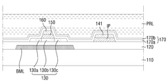
도 29를 참조하면, 제2 층간 절연막(170b) 상부에 감광막 물질층(PRL)을 도포하는 단계까지는 상술한 도 2 내지 도 17의 실시예와 실질적으로 동일하다. Referring to FIG. 29, the step of applying the photoresist material layer PRL on the second
이어, 도 30을 참조하면, 제2 층간 절연막(170b) 상부에 감광막 물질층(PRL)을 도포하고, 제4 마스크(M4)를 통하여 제4 감광막 패턴(PR4)을 형성한다. Next, referring to FIG. 30, the photoresist material layer PRL is coated on the second
제4 마스크(M4)는 광을 투과시키는 광투과부(TA), 광을 차단하는 광차단부(PA)를 포함할 수 있다. 제4 마스크(MA4)의 광 투과부(TA)는 제1 컨택홀(CNT1) 및 제2 컨택홀(CNT2)이 형성될 영역에 대응되도록 배치하고, 제4 마스크(MA4)를 통하여 감광막에 광을 조사한 후(노광), 감광막을 현상(develop)하면 광투과부(TA)에 대응하는 감광막 영역이 제거되고, 광차단부(PA)에 대응하는 감광막 영역이 남게 된다. The fourth mask M4 may include a light transmission part TA for transmitting light and a light blocking part PA for blocking light. The light transmitting part TA of the fourth mask MA4 is disposed so as to correspond to a region where the first contact hole CNT1 and the second contact hole CNT2 are to be formed, and emits light to the photosensitive film through the fourth mask MA4. After irradiation (exposure), when the photosensitive film is developed, the photosensitive film area corresponding to the light transmitting part TA is removed, and the photosensitive film area corresponding to the light blocking part PA remains.
구체적으로, 광투과부(TA)에 대응되는 영역에는 제1 홀(H1), 제2 홀(H2) 및 제3 홀(H3)이 형성된다. 일 실시예와 달리 본 발명의 다른 실시예에서는 잔여 감광물(도 18의 RP) 없이 제1 홀(H1), 제2 홀(H2) 및 제3 홀(H3) 각각이 제2 층간 절연막(170b)을 노출시키게 된다.In detail, the first hole H1, the second hole H2, and the third hole H3 are formed in an area corresponding to the light transmitting part TA. Unlike one embodiment, in another embodiment of the present invention, each of the first hole H1, the second hole H2, and the third hole H3 without the remaining photoresist (RP of FIG. 18) is the second interlayer insulating layer 170b. ) Will be exposed.
예시적인 실시예에서, 게이트 전극(160)에 대응되는 제2 층간 절역막(170b) 상에 형성되는 제4 감광막 패턴(PR4)의 두께는 17000Å일 수 있다. 다만, 이에 한정되는 것은 아니며, 제1, 제2 층간 절연막(170a, 170b) 및 버퍼층(120)의 물질, 두께, 에칭시 사용되는 혼합가스 등에 따라 다양하게 변형될 수 있다.In an exemplary embodiment, the thickness of the fourth photoresist pattern PR4 formed on the second
도 30 및 도 31을 참조하면, 제4 감광막 패턴(PR4)을 식각 마스크로 하여 제2 층간 절연막(170b), 제1 층간 절연막(170a) 및 버퍼층(120)을 식각한 후, 제4 감광막 패턴(PR4)을 제거하여, 하부 전극패턴(BML)을 노출하는 제1 컨택홀(CNT1)과 소스 영역(130a) 및 드레인 영역(130c)을 각각 노출하는 제2 컨택홀(CNT2)을 형성할 수 있다.30 and 31, after etching the second
제1 층간 절연막(170a)의 두께(d1)가 제2 층간 절연막(170a)의 두께(d2)보다 두껍게 형성될 수 있으며, 버퍼층(120)이 두께(d3)는 잔여 감광물(RP)의 두께(D2)보다 얇게 형성될 수 있다. 예시적인 실시예에서, 잔여 감광물(RP)의 두께(D2)는 7000Å인 경우, 버퍼층(120)의 두께(d3)은 7000Å이하로 형성될 수 있다. 그리고, 제2 층간 절연막(170b), 제1 층간 절연막(170a) 및 버퍼층(120)을 SiOx물질로 형성될 수 있다.The thickness d1 of the first
그리고, 식각시 사용되는 혼합가스는 SiOx/IGZO 식각 선택비가 40(40:1)보다 클 수 있다. 예를 들어, 식각시 사용되는 혼합가스는 C4F8과 Ar의 혼합가스이거나, CHF3와 Ar의 혼합가스일 수 있으나, 이에 한정되는 것은 아니다.In addition, the mixed gas used for etching may have a SiOx / IGZO etching selectivity greater than 40 (40: 1). For example, the mixed gas used for etching may be a mixed gas of C 4 F 8 and Ar, or a mixed gas of CHF 3 and Ar, but is not limited thereto.
식각시 사용되는 혼합가스가 CHF3와 Ar의 혼합가스인 경우 SiOx/IGZO 식각 선택비가 50(50:1)보다 크게 나타나며, C4F8 와 Ar의 혼합가스인 경우 SiOx / IGZO 식각 선택비가 100(100:1)보다 크게 나타난다. When the mixed gas used for etching is a mixed gas of CHF 3 and Ar, the SiOx / IGZO etching selectivity is greater than 50 (50: 1), and when the mixed gas of C 4 F 8 and Ar is SiOx / IGZO etching selectivity of 100 Greater than (100: 1).
따라서, 제1 컨택홀(CNT1)과 제2 컨택홀(CNT2)을 하나의 마스크로 동시에 형성하는 경우에도 제1 컨택홀(CNT1)을 형성하기 위하여 제1, 제2 층간 절연막(170a, 170b) 및 버퍼층(120)을 식각하는 동안에 제2 컨택홀(CNT2) 형성 영역에 제1, 제2 층간 절연막(170a, 170b)이 식각되고, IGZO로 이루어진 소스 및 드레인 영역(130a, 130b)이 노출되어도, IGZO로 이루어진 소스 및 드레인 영역(130a, 130b)이 손상을 최소화할 수 있게 된다. 이에 따라, 서로 깊이가 다르게 형성되는 하부 전극패턴(BML)을 노출하는 제1 컨택홀(CNT1)과 소스 영역 및 드레인 영역(130a, 130b) 각각을 노출하는 제2 컨택홀(CNT2)을 C4F8과 Ar의 혼합가스 또는 CHF3와 Ar의 혼합가스를 이용하여 동시에 식각할 수 있게 된다. Therefore, even when the first contact hole CNT1 and the second contact hole CNT2 are simultaneously formed with one mask, the first and second
이에 따라, 종래 하부 전극패턴(BML)을 연결하는 제1 컨택홀(CNT1)과 소스 영역 및 드레인 영역(130a, 130b)을 노출하는 제2 컨택홀(CNT2)을 형성하기 위하여 5개의 마스크를 이용하였던 공정에 비하여 4개의 마스크(M1, M2, M3, M4)를 이용하여, 하부 전극패턴(BML)을 노출하는 제1 컨택홀(CNT1)과 소스 영역 및 드레인 영역(130a, 130b)을 노출하는 제2 컨택홀(CNT2)을 형성할 수 있게 되어 제조비용을 절감시킴과 동시에 생산성을 향상시킬 수 있게 된다.Accordingly, five masks are used to form the first contact hole CNT1 connecting the lower electrode pattern BML and the second contact hole CNT2 exposing the source and
이후 공정은 전술한 실시예와 실질적으로 동일하므로 중복 설명은 생략하기로 한다. Since the process is substantially the same as the above-described embodiment, duplicate description will be omitted.
이상 첨부된 도면을 참조하여 본 발명의 실시예들을 설명하였지만, 본 발명이 속하는 기술분야에서 통상의 지식을 가진 자는 본 발명의 그 기술적 사상이나 필수적인 특징을 변경하지 않고서 다른 구체적인 형태로 실시될 수 있다는 것을 이해할 수 있을 것이다. 그러므로 이상에서 기술한 실시예들은 모든 면에서 예시적인 것이며 한정적이 아닌 것으로 이해해야만 한다.Although embodiments of the present invention have been described above with reference to the accompanying drawings, those skilled in the art to which the present invention pertains may be embodied in other specific forms without changing the technical spirit or essential features of the present invention. I can understand that. Therefore, it should be understood that the embodiments described above are exemplary in all respects and not restrictive.
100: 유기발광 표시장치 120: 버퍼층
130: 반도체층 141: 제1 커패시터 전극
142: 제2 커패시터 전극 150: 게이트 절연막
160: 게이트 전극 170: 층간 절연막
181: 화소 전극 182: 화소정의막
191: 제1 전극 192: 제2 전극
BML: 하부 전극패턴 CNT1: 제1 컨택홀
CNT2: 제2 컨택홀 CNT3: 제3 컨택홀 100: organic light emitting display 120: buffer layer
130: semiconductor layer 141: first capacitor electrode
142: second capacitor electrode 150: gate insulating film
160: gate electrode 170: interlayer insulating film
181: pixel electrode 182: pixel defining film
191: first electrode 192: second electrode
BML: Lower electrode pattern CNT1: First contact hole
CNT2: second contact hole CNT3: third contact hole
Claims (23)
상기 버퍼층 상에 산화물 반도체층을 포함하는 박막 트랜지스터를 형성하는 단계;
상기 박막 트랜지스터 상에 층간 절연막을 형성하는 단계;
상기 층간 절연막 상에 서로 깊이가 다른 제1 홀과 제2 홀을 포함하는 감광막 패턴을 형성하는 단계; 및
상기 감광막 패턴을 이용하여 상기 하부 전극패턴을 노출시키는 제1 컨택홀과 상기 산화물 반도체층을 노출시키는 제2 컨택홀을 동시에 형성하는 단계를 포함하는 유기발광 표시장치의 제조방법.
Forming a lower electrode pattern on the substrate including the transistor region and the capacitor region corresponding to the transistor region, and forming a buffer layer on the substrate including the lower electrode pattern;
Forming a thin film transistor including an oxide semiconductor layer on the buffer layer;
Forming an interlayer insulating film on the thin film transistor;
Forming a photoresist pattern including a first hole and a second hole having a different depth from each other on the interlayer insulating film; And
And simultaneously forming a first contact hole exposing the lower electrode pattern and a second contact hole exposing the oxide semiconductor layer using the photoresist pattern.
상기 산화물 반도체층은 소스 영역, 채널 영역 및 드레인 영역을 포함하며, 상기 제2 컨택홀은 상기 소스 영역과 상기 드레인 영역을 각각 노출시키는 유기발광 표시장치의 제조방법.
The method of claim 1,
The oxide semiconductor layer includes a source region, a channel region, and a drain region, and the second contact hole exposes the source region and the drain region, respectively.
상기 층간 절연막은, 상기 버퍼층 상부에 제2 층간 절연막과, 상기 제2 층간 절연막과 상기 버퍼층 사이에 배치되는 제1 층간 절연막을 포함하며, 상기 제2 층간 절연막보다 상기 제1 층간 절연막이 더 두꺼운 유기발광 표시장치의 제조방법.The method of claim 2,
The interlayer insulating film includes a second interlayer insulating film on the buffer layer, and a first interlayer insulating film disposed between the second interlayer insulating film and the buffer layer, wherein the first interlayer insulating film is thicker than the second interlayer insulating film. Method of manufacturing a light emitting display device.
상기 감광막 패턴은 광투과부, 광차단부 및 반투과부를 포함하는 하프톤 마스크를 이용하여 형성되며,
상기 감광막 패턴을 형성하는 단계는, 상기 광투과부에 대응하여 상기 제1 홀을 형성하고 상기 반투과부에 대응하여 상기 제2 홀을 형성하는 단계를 더 포함하는 유기발광 표시장치의 제조방법.
The method of claim 3, wherein
The photoresist pattern is formed using a halftone mask including a light transmitting portion, a light blocking portion, and a semitransmissive portion,
The forming of the photoresist pattern may further include forming the first hole corresponding to the light transmitting part and forming the second hole corresponding to the transflective part.
상기 제1 홀은 상기 제1 컨택홀에 대응하여 상기 제2 층간 절연막을 노출시키고, 상기 제2 홀은 상기 제2 컨택홀에 대응하여 잔여 감광물을 노출시키는 유기발광 표시장치의 제조방법.
The method of claim 4, wherein
And the first hole exposes the second interlayer insulating layer corresponding to the first contact hole, and the second hole exposes the remaining photosensitive material corresponding to the second contact hole.
상기 잔여 감광물의 두께는 상기 버퍼층의 두께보다 두꺼운 유기발광 표시장치의 제조방법.
The method of claim 5,
And a thickness of the remaining photoresist is thicker than a thickness of the buffer layer.
상기 제2 층간 절연막의 에칭 레이트(etching rate)는 상기 제1 층간 절연막 및 상기 버퍼층의 에칭 레이트(etching rate)보다 큰 유기발광 표시장치의 제조방법.
The method of claim 5,
The etching rate of the second interlayer insulating layer is greater than the etching rate of the first interlayer insulating layer and the buffer layer.
상기 제1 층간 절연막과 상기 버퍼층은 에칭 레이트(etching rate)가 동일한 유기발광 표시장치의 제조방법.
The method of claim 5,
The first interlayer insulating layer and the buffer layer have the same etching rate.
상기 잔여 감광물의 에칭 레이트(etching rate)는 상기 버퍼층의 에칭 레이트(etching rate)보다 큰 유기발광 표시장치의 제조방법.
The method of claim 5,
The etching rate of the remaining photoresist is greater than the etching rate of the buffer layer.
상기 제1 컨택홀과 상기 제2 컨택홀을 형성하는 단계는,
NF3 및 O2의 혼합가스를 이용하여 상기 제1 컨택홀에 대응하여 상기 제1, 제2 층간 절연막 및 상기 버퍼층을 식각하고, 상기 제2 컨택홀에 대응하여 상기 잔여 감광물 및 상기 제1, 제2 층간 절연막을 식각하는 단계를 더 포함하는 유기발광 표시장치의 제조방법.
The method of claim 9,
Forming the first contact hole and the second contact hole,
The first and second interlayer insulating layers and the buffer layer are etched in correspondence with the first contact holes using a mixed gas of NF 3 and O 2, and the residual photoresist and the first and second parts corresponding to the second contact holes are etched. A method of manufacturing an organic light emitting display device, the method comprising: etching the interlayer insulating film.
상기 제1 층간 절연막 및 상기 버퍼층의 에칭 레이트(etching rate)는 2185Å/min이며, 상기 잔여 감광물의 에칭 레이트(etching rate)는 3825Å/min인 유기발광 표시장치의 제조방법.
The method of claim 10,
An etching rate of the first interlayer insulating layer and the buffer layer is 2185 Å / min, and an etching rate of the remaining photosensitive material is 3825 Å / min.
상기 산화물 반도체층은 IGZO로 이루어지며, 상기 산화물 반도체층의 에칭 레이트(etching rate)는 190Å/min인 유기발광 표시장치의 제조방법.
The method of claim 11,
The oxide semiconductor layer is made of IGZO, and the etching rate of the oxide semiconductor layer is 190 kW / min.
상기 제1 컨택홀을 통하여 소스 전극과 상기 하부 전극패턴이 전기적으로 연결되고, 상기 소스 영역에 형성된 제2 컨택홀을 통하여 상기 소스 전극과 상기 산화물 반도체층의 소스 영역이 전기적으로 연결되는 유기발광 표시장치의 제조방법.
The method of claim 12,
An organic light emitting display in which a source electrode and the lower electrode pattern are electrically connected through the first contact hole, and the source electrode and the source region of the oxide semiconductor layer are electrically connected through a second contact hole formed in the source region Method of manufacturing the device.
상기 버퍼층 상에 산화물 반도체층을 포함하는 박막 트랜지스터를 형성하는 단계;
상기 박막 트랜지스터 상에 층간 절연막을 형성하는 단계;
상기 층간 절연막 상에 마스크를 이용하여 상기 층간 절연막을 각각 노출시키는 제1 홀 및 제2 홀을 포함하는 감광막 패턴을 형성하는 단계; 및
상기 감광막 패턴을 이용하여 상기 하부 전극패턴을 노출시키는 제1 컨택홀과 상기 산화물 반도체층을 노출시키는 제2 컨택홀을 동시에 형성하는 단계를 포함하는 유기발광 표시장치의 제조방법.
Forming a lower electrode pattern on the substrate including the transistor region and the capacitor region corresponding to the transistor region, and forming a buffer layer on the substrate including the lower electrode pattern;
Forming a thin film transistor including an oxide semiconductor layer on the buffer layer;
Forming an interlayer insulating film on the thin film transistor;
Forming a photoresist pattern on the interlayer insulating layer, the photoresist pattern including a first hole and a second hole exposing the interlayer insulating layer, respectively, using a mask; And
And simultaneously forming a first contact hole exposing the lower electrode pattern and a second contact hole exposing the oxide semiconductor layer using the photoresist pattern.
상기 제1 홀은 상기 제1 컨택홀에 대응하여 상기 층간 절연막을 노출시키고, 상기 제2 홀은 상기 제2 컨택홀에 대응하여 상기 층간 절연막을 노출시키는 유기발광 표시장치의 제조방법.
The method of claim 14,
And the first hole exposes the interlayer insulating layer corresponding to the first contact hole, and the second hole exposes the interlayer insulating layer corresponding to the second contact hole.
상기 산화물 반도체층은 소스 영역, 채널 영역 및 드레인 영역을 포함하며 상기 제2 컨택홀은 상기 소스 영역과 상기 드레인 영역을 각각 노출시키는 유기발광 표시장치의 제조방법.
The method of claim 15,
The oxide semiconductor layer includes a source region, a channel region, and a drain region, and the second contact hole exposes the source region and the drain region, respectively.
상기 층간 절연막 및 상기 버퍼층은 SiOx로 이루어지며, 상기 산화물 반도체층은 IGZO로 이루어지고,
상기 제1 컨택홀과 상기 제2 컨택홀을 형성하는 단계는,
SiOx / IGZO 식각 선택비가 40보다 큰 혼합가스를 이용하여 식각하는 단계를 더 포함하는 유기발광 표시장치의 제조방법.
The method of claim 16,
The interlayer insulating layer and the buffer layer is made of SiOx, the oxide semiconductor layer is made of IGZO,
Forming the first contact hole and the second contact hole,
A method of manufacturing an organic light emitting display device, the method comprising: etching using a mixed gas having a SiOx / IGZO etching selectivity greater than 40.
상기 혼합가스는 C4F8과 Ar의 혼합가스인 유기발광 표시장치의 제조방법.
The method of claim 17,
And the mixed gas is a mixed gas of C 4 F 8 and Ar.
상기 혼합가스는 CHF3와 Ar의 혼합가스인 유기발광 표시장치의 제조방법.
The method of claim 17,
And the mixed gas is a mixed gas of CHF 3 and Ar.
상기 제1 컨택홀을 통하여 소스 전극과 상기 하부 전극패턴이 전기적으로 연결되고, 상기 소스 영역에 형성된 상기 제2 컨택홀을 통하여 상기 소스 전극과 상기 산화물 반도체층의 소스 영역이 전기적으로 연결되는 유기발광 표시장치의 제조방법.
The method of claim 17,
An organic light emitting diode in which a source electrode and the lower electrode pattern are electrically connected through the first contact hole, and the source electrode and the source region of the oxide semiconductor layer are electrically connected through the second contact hole formed in the source region Method for manufacturing a display device.
상기 제2 절연층 상에 서로 깊이가 다른 제1 홀과 제2 홀을 포함하는 마스크 패턴을 형성하는 단계; 및
상기 마스크 패턴의 상기 제1 홀의 하부 구조물 및 상기 제2 홀의 하부 구조물을 동시에 식각하여 상기 제1 패턴을 노출하는 제1 컨택홀 및 상기 제2 패턴을 노출하는 제2 컨택홀을 형성하는 단계를 포함하는 유기발광 표시장치의 제조방법.
Preparing a substrate on which a first pattern, a first insulating layer covering the first pattern, and a second pattern on the first insulating layer and a second insulating layer on the second pattern are sequentially disposed;
Forming a mask pattern on the second insulating layer, the mask pattern including first and second holes having different depths; And
Simultaneously etching the lower structure of the first hole and the lower structure of the second hole of the mask pattern to form a first contact hole exposing the first pattern and a second contact hole exposing the second pattern A method of manufacturing an organic light emitting display device.
상기 제1 패턴은 하부 전극패턴이고, 상기 제2 패턴은 산화물 반도체층인 유기발광 표시장치의 제조방법.
The method of claim 21,
The first pattern is a lower electrode pattern, and the second pattern is an oxide semiconductor layer.
상기 마스크 패턴은 광투과부, 광차단부 및 반투과부를 포함하는 하프톤 마스크를 이용하여 형성되는 감광막 패턴이며,
상기 감광막 패턴은 상기 광투과부에 대응하여 상기 제1 홀을 형성하고 상기 반투과부에 대응하여 상기 제2 홀을 형성하는 단계를 더 포함하는 유기발광 표시장치의 제조방법.
The method of claim 22,
The mask pattern is a photosensitive film pattern formed using a halftone mask including a light transmitting portion, a light blocking portion, and a semi-transmissive portion.
The photoresist pattern may further include forming the first hole corresponding to the light transmitting part and forming the second hole corresponding to the transflective part.
Priority Applications (4)
| Application Number | Priority Date | Filing Date | Title |
|---|---|---|---|
| KR1020180072844A KR102635447B1 (en) | 2018-06-25 | 2018-06-25 | Method for manufacturing organic light emitting display |
| US17/255,406 US20210376243A1 (en) | 2018-06-25 | 2018-12-21 | Method of manufacturing organic light-emitting display device |
| CN201880095019.5A CN112352332A (en) | 2018-06-25 | 2018-12-21 | Method of manufacturing organic light emitting display device |
| PCT/KR2018/016441 WO2020004747A1 (en) | 2018-06-25 | 2018-12-21 | Method of manufacturing organic light-emitting display device |
Applications Claiming Priority (1)
| Application Number | Priority Date | Filing Date | Title |
|---|---|---|---|
| KR1020180072844A KR102635447B1 (en) | 2018-06-25 | 2018-06-25 | Method for manufacturing organic light emitting display |
Publications (2)
| Publication Number | Publication Date |
|---|---|
| KR20200000856A true KR20200000856A (en) | 2020-01-06 |
| KR102635447B1 KR102635447B1 (en) | 2024-02-08 |
Family
ID=68987152
Family Applications (1)
| Application Number | Title | Priority Date | Filing Date |
|---|---|---|---|
| KR1020180072844A KR102635447B1 (en) | 2018-06-25 | 2018-06-25 | Method for manufacturing organic light emitting display |
Country Status (4)
| Country | Link |
|---|---|
| US (1) | US20210376243A1 (en) |
| KR (1) | KR102635447B1 (en) |
| CN (1) | CN112352332A (en) |
| WO (1) | WO2020004747A1 (en) |
Cited By (2)
| Publication number | Priority date | Publication date | Assignee | Title |
|---|---|---|---|---|
| US11825706B2 (en) | 2020-05-12 | 2023-11-21 | Samsung Display Co., Ltd. | Display apparatus having bridge electrode electrically connecting lower electrode pattern layer and semiconductor layer of transistor |
| US11844256B2 (en) | 2020-11-12 | 2023-12-12 | Samsung Display Co., Ltd. | Display device including third conductive layer directly contacting first conductive layer and second conductive layer |
Citations (1)
| Publication number | Priority date | Publication date | Assignee | Title |
|---|---|---|---|---|
| KR20170124151A (en) * | 2016-04-29 | 2017-11-10 | 삼성디스플레이 주식회사 | Transistor array panel and manufacturing method thereof |
Family Cites Families (8)
| Publication number | Priority date | Publication date | Assignee | Title |
|---|---|---|---|---|
| US6380559B1 (en) * | 1999-06-03 | 2002-04-30 | Samsung Electronics Co., Ltd. | Thin film transistor array substrate for a liquid crystal display |
| TWI621270B (en) * | 2013-02-07 | 2018-04-11 | 群創光電股份有限公司 | Thin-film transistor device and thin-film transistor display apparatus |
| KR102094847B1 (en) * | 2013-07-03 | 2020-03-31 | 삼성디스플레이 주식회사 | Display substrate having a thin film transistor and method of manufacturing the same |
| CN103715141B (en) * | 2013-12-27 | 2015-02-18 | 京东方科技集团股份有限公司 | Array substrate and preparation method thereof |
| KR102188067B1 (en) * | 2014-05-27 | 2020-12-07 | 엘지디스플레이 주식회사 | Thin Film Transistor Array Substrate and Method for Manufacturing the Same |
| CN104022126B (en) * | 2014-05-28 | 2017-04-12 | 京东方科技集团股份有限公司 | Array substrate and manufacturing method thereof, and display apparatus |
| KR102649257B1 (en) * | 2016-09-30 | 2024-03-19 | 엘지디스플레이 주식회사 | Organic light emitting display device and method of manufacturing the same |
| CN107946196B (en) * | 2017-11-28 | 2021-12-28 | 合肥鑫晟光电科技有限公司 | Oxide thin film transistor, preparation method thereof, array substrate and display device |
-
2018
- 2018-06-25 KR KR1020180072844A patent/KR102635447B1/en active IP Right Grant
- 2018-12-21 US US17/255,406 patent/US20210376243A1/en active Pending
- 2018-12-21 WO PCT/KR2018/016441 patent/WO2020004747A1/en active Application Filing
- 2018-12-21 CN CN201880095019.5A patent/CN112352332A/en active Pending
Patent Citations (1)
| Publication number | Priority date | Publication date | Assignee | Title |
|---|---|---|---|---|
| KR20170124151A (en) * | 2016-04-29 | 2017-11-10 | 삼성디스플레이 주식회사 | Transistor array panel and manufacturing method thereof |
Cited By (2)
| Publication number | Priority date | Publication date | Assignee | Title |
|---|---|---|---|---|
| US11825706B2 (en) | 2020-05-12 | 2023-11-21 | Samsung Display Co., Ltd. | Display apparatus having bridge electrode electrically connecting lower electrode pattern layer and semiconductor layer of transistor |
| US11844256B2 (en) | 2020-11-12 | 2023-12-12 | Samsung Display Co., Ltd. | Display device including third conductive layer directly contacting first conductive layer and second conductive layer |
Also Published As
| Publication number | Publication date |
|---|---|
| CN112352332A (en) | 2021-02-09 |
| WO2020004747A1 (en) | 2020-01-02 |
| US20210376243A1 (en) | 2021-12-02 |
| KR102635447B1 (en) | 2024-02-08 |
Similar Documents
| Publication | Publication Date | Title |
|---|---|---|
| KR100964229B1 (en) | Organic light emitting display apparatus and method of manufacturing thereof | |
| US9548321B2 (en) | Method of manufacturing thin film transistor (TFT) array substrate | |
| JP5851192B2 (en) | Organic light emitting display device and method for manufacturing the same | |
| JP6054629B2 (en) | Backplane for flat panel display, flat panel display including the same, and manufacturing method thereof | |
| US8835203B2 (en) | Organic light emitting diode display and method for manufacturing the same | |
| TWI580023B (en) | Organic light-emitting display apparatus and method of manufacturing the same | |
| US9761651B2 (en) | Transparent organic light emitting display apparatus and method of manufacturing the same | |
| US8614462B2 (en) | Array substrate for organic electroluminescent device and method of fabricating the same | |
| US8716702B2 (en) | Organic light-emitting display device and method of manufacturing the same | |
| US9577114B2 (en) | Transistors, methods of forming transistors and display devices having transistors | |
| KR20120080887A (en) | Organic light emitting display and method for manufacturing thereof | |
| TWI629767B (en) | Organic light-emitting display apparatus | |
| US20150357356A1 (en) | Thin film transistor array substrate and method of manufacturing the same | |
| KR101777247B1 (en) | Organic light emitting display device and manufacturing method of the same | |
| KR20150040668A (en) | Organic light-emitting display apparatus and method for manufacturing the same | |
| KR20120061312A (en) | Organic light emitting display device and method of manufacturing the same | |
| KR20150030034A (en) | display apparatus and manufacturing method for the same | |
| KR102635447B1 (en) | Method for manufacturing organic light emitting display | |
| KR20150070839A (en) | Method of manufacturing display apparatus | |
| KR20150084142A (en) | Thin film transistor, method of manufacturing the thin film transistor and falt panel display device having the thin film transistor | |
| KR102437165B1 (en) | Organic light emitting display device and method of manufacturing the same | |
| KR20240022051A (en) | Deposition device and manufacturing method for display device by using the same | |
| KR20200019163A (en) | Organic light emitting display apparatus and manufacturing method thereof | |
| KR20070120343A (en) | Organic electro-luminescence display and fabricating method thereof |
Legal Events
| Date | Code | Title | Description |
|---|---|---|---|
| A201 | Request for examination | ||
| E902 | Notification of reason for refusal | ||
| E90F | Notification of reason for final refusal | ||
| E701 | Decision to grant or registration of patent right | ||
| GRNT | Written decision to grant |