KR20180108918A - Enhanced bulk heterojunction devices prepared by thermal and solvent vapor annealing processes - Google Patents
Enhanced bulk heterojunction devices prepared by thermal and solvent vapor annealing processes Download PDFInfo
- Publication number
- KR20180108918A KR20180108918A KR1020187027845A KR20187027845A KR20180108918A KR 20180108918 A KR20180108918 A KR 20180108918A KR 1020187027845 A KR1020187027845 A KR 1020187027845A KR 20187027845 A KR20187027845 A KR 20187027845A KR 20180108918 A KR20180108918 A KR 20180108918A
- Authority
- KR
- South Korea
- Prior art keywords
- solvent
- annealing
- annealed
- bulk
- organic
- Prior art date
Links
- 238000000034 method Methods 0.000 title claims abstract description 39
- 238000000654 solvent vapour annealing Methods 0.000 title abstract description 16
- 230000008569 process Effects 0.000 title description 21
- 239000002904 solvent Substances 0.000 claims abstract description 100
- 239000000463 material Substances 0.000 claims abstract description 68
- 238000004519 manufacturing process Methods 0.000 claims abstract description 13
- 230000008016 vaporization Effects 0.000 claims description 4
- 238000000137 annealing Methods 0.000 abstract description 86
- 238000004528 spin coating Methods 0.000 abstract description 7
- 238000013086 organic photovoltaic Methods 0.000 abstract description 6
- YMWUJEATGCHHMB-UHFFFAOYSA-N Dichloromethane Chemical compound ClCCl YMWUJEATGCHHMB-UHFFFAOYSA-N 0.000 description 180
- IHXWECHPYNPJRR-UHFFFAOYSA-N 3-hydroxycyclobut-2-en-1-one Chemical compound OC1=CC(=O)C1 IHXWECHPYNPJRR-UHFFFAOYSA-N 0.000 description 115
- 239000010408 film Substances 0.000 description 24
- 239000000203 mixture Substances 0.000 description 22
- HEDRZPFGACZZDS-UHFFFAOYSA-N Chloroform Chemical compound ClC(Cl)Cl HEDRZPFGACZZDS-UHFFFAOYSA-N 0.000 description 20
- 230000001965 increasing effect Effects 0.000 description 20
- 239000010410 layer Substances 0.000 description 20
- RFFLAFLAYFXFSW-UHFFFAOYSA-N 1,2-dichlorobenzene Chemical compound ClC1=CC=CC=C1Cl RFFLAFLAYFXFSW-UHFFFAOYSA-N 0.000 description 18
- 238000002441 X-ray diffraction Methods 0.000 description 18
- 150000003384 small molecules Chemical class 0.000 description 12
- 238000005266 casting Methods 0.000 description 11
- 239000011368 organic material Substances 0.000 description 11
- 238000010521 absorption reaction Methods 0.000 description 10
- 238000005191 phase separation Methods 0.000 description 10
- 239000004065 semiconductor Substances 0.000 description 10
- 229910052751 metal Inorganic materials 0.000 description 9
- 239000002184 metal Substances 0.000 description 9
- 238000005424 photoluminescence Methods 0.000 description 9
- 238000009835 boiling Methods 0.000 description 8
- 238000001514 detection method Methods 0.000 description 8
- 230000005670 electromagnetic radiation Effects 0.000 description 8
- 238000005286 illumination Methods 0.000 description 8
- 238000005259 measurement Methods 0.000 description 8
- 230000003287 optical effect Effects 0.000 description 8
- 230000005693 optoelectronics Effects 0.000 description 8
- 238000010494 dissociation reaction Methods 0.000 description 7
- 230000005593 dissociations Effects 0.000 description 7
- 239000012528 membrane Substances 0.000 description 7
- 239000000758 substrate Substances 0.000 description 7
- 239000010409 thin film Substances 0.000 description 7
- 230000008859 change Effects 0.000 description 6
- 239000002800 charge carrier Substances 0.000 description 6
- 230000005855 radiation Effects 0.000 description 6
- 238000004833 X-ray photoelectron spectroscopy Methods 0.000 description 5
- 239000013078 crystal Substances 0.000 description 5
- 238000009792 diffusion process Methods 0.000 description 5
- 230000005284 excitation Effects 0.000 description 5
- 239000011521 glass Substances 0.000 description 5
- 229920000642 polymer Polymers 0.000 description 5
- 230000004044 response Effects 0.000 description 5
- 230000003595 spectral effect Effects 0.000 description 5
- XLOMVQKBTHCTTD-UHFFFAOYSA-N Zinc monoxide Chemical compound [Zn]=O XLOMVQKBTHCTTD-UHFFFAOYSA-N 0.000 description 4
- 238000004220 aggregation Methods 0.000 description 4
- 230000002776 aggregation Effects 0.000 description 4
- 229910021417 amorphous silicon Inorganic materials 0.000 description 4
- 230000008033 biological extinction Effects 0.000 description 4
- 238000006243 chemical reaction Methods 0.000 description 4
- 230000000694 effects Effects 0.000 description 4
- 230000005684 electric field Effects 0.000 description 4
- 230000005611 electricity Effects 0.000 description 4
- 238000001704 evaporation Methods 0.000 description 4
- AMGQUBHHOARCQH-UHFFFAOYSA-N indium;oxotin Chemical compound [In].[Sn]=O AMGQUBHHOARCQH-UHFFFAOYSA-N 0.000 description 4
- 239000012044 organic layer Substances 0.000 description 4
- 238000007788 roughening Methods 0.000 description 4
- 238000000089 atomic force micrograph Methods 0.000 description 3
- 230000007423 decrease Effects 0.000 description 3
- 239000000412 dendrimer Substances 0.000 description 3
- 229920000736 dendritic polymer Polymers 0.000 description 3
- 238000000151 deposition Methods 0.000 description 3
- 229910000476 molybdenum oxide Inorganic materials 0.000 description 3
- 239000000243 solution Substances 0.000 description 3
- 229910052720 vanadium Inorganic materials 0.000 description 3
- XLYOFNOQVPJJNP-UHFFFAOYSA-N water Substances O XLYOFNOQVPJJNP-UHFFFAOYSA-N 0.000 description 3
- XQNMSKCVXVXEJT-UHFFFAOYSA-N 7,14,25,32-tetrazaundecacyclo[21.13.2.22,5.03,19.04,16.06,14.08,13.020,37.024,32.026,31.034,38]tetraconta-1(36),2,4,6,8,10,12,16,18,20(37),21,23(38),24,26,28,30,34,39-octadecaene-15,33-dione 7,14,25,32-tetrazaundecacyclo[21.13.2.22,5.03,19.04,16.06,14.08,13.020,37.025,33.026,31.034,38]tetraconta-1(37),2,4,6,8,10,12,16,18,20,22,26,28,30,32,34(38),35,39-octadecaene-15,24-dione Chemical compound O=c1c2ccc3c4ccc5c6nc7ccccc7n6c(=O)c6ccc(c7ccc(c8nc9ccccc9n18)c2c37)c4c56.O=c1c2ccc3c4ccc5c6c(ccc(c7ccc(c8nc9ccccc9n18)c2c37)c46)c1nc2ccccc2n1c5=O XQNMSKCVXVXEJT-UHFFFAOYSA-N 0.000 description 2
- IJGRMHOSHXDMSA-UHFFFAOYSA-N Atomic nitrogen Chemical compound N#N IJGRMHOSHXDMSA-UHFFFAOYSA-N 0.000 description 2
- 238000000862 absorption spectrum Methods 0.000 description 2
- 238000004630 atomic force microscopy Methods 0.000 description 2
- 230000004888 barrier function Effects 0.000 description 2
- 239000000969 carrier Substances 0.000 description 2
- 229920001940 conductive polymer Polymers 0.000 description 2
- 230000001276 controlling effect Effects 0.000 description 2
- XCJYREBRNVKWGJ-UHFFFAOYSA-N copper(II) phthalocyanine Chemical compound [Cu+2].C12=CC=CC=C2C(N=C2[N-]C(C3=CC=CC=C32)=N2)=NC1=NC([C]1C=CC=CC1=1)=NC=1N=C1[C]3C=CC=CC3=C2[N-]1 XCJYREBRNVKWGJ-UHFFFAOYSA-N 0.000 description 2
- 238000012937 correction Methods 0.000 description 2
- 229910021419 crystalline silicon Inorganic materials 0.000 description 2
- 230000003247 decreasing effect Effects 0.000 description 2
- 230000007547 defect Effects 0.000 description 2
- 230000008021 deposition Effects 0.000 description 2
- 230000002708 enhancing effect Effects 0.000 description 2
- 230000008020 evaporation Effects 0.000 description 2
- 238000000605 extraction Methods 0.000 description 2
- 238000011049 filling Methods 0.000 description 2
- 230000006870 function Effects 0.000 description 2
- 125000001183 hydrocarbyl group Chemical group 0.000 description 2
- 230000006872 improvement Effects 0.000 description 2
- 239000012535 impurity Substances 0.000 description 2
- 239000007769 metal material Substances 0.000 description 2
- 229920000767 polyaniline Polymers 0.000 description 2
- 239000010453 quartz Substances 0.000 description 2
- 230000009467 reduction Effects 0.000 description 2
- 238000011160 research Methods 0.000 description 2
- 238000010079 rubber tapping Methods 0.000 description 2
- 229920006395 saturated elastomer Polymers 0.000 description 2
- 238000000926 separation method Methods 0.000 description 2
- VYPSYNLAJGMNEJ-UHFFFAOYSA-N silicon dioxide Inorganic materials O=[Si]=O VYPSYNLAJGMNEJ-UHFFFAOYSA-N 0.000 description 2
- 238000010561 standard procedure Methods 0.000 description 2
- PMJMHCXAGMRGBZ-UHFFFAOYSA-N subphthalocyanine Chemical compound N1C(N=C2C3=CC=CC=C3C(=N3)N2)=C(C=CC=C2)C2=C1N=C1C2=CC=CC=C2C3=N1 PMJMHCXAGMRGBZ-UHFFFAOYSA-N 0.000 description 2
- 238000012360 testing method Methods 0.000 description 2
- 238000002207 thermal evaporation Methods 0.000 description 2
- XOLBLPGZBRYERU-UHFFFAOYSA-N tin dioxide Chemical compound O=[Sn]=O XOLBLPGZBRYERU-UHFFFAOYSA-N 0.000 description 2
- 229910001887 tin oxide Inorganic materials 0.000 description 2
- 238000012546 transfer Methods 0.000 description 2
- 238000004627 transmission electron microscopy Methods 0.000 description 2
- 238000001947 vapour-phase growth Methods 0.000 description 2
- 239000011787 zinc oxide Substances 0.000 description 2
- RTZYCRSRNSTRGC-LNTINUHCSA-K (z)-4-oxopent-2-en-2-olate;ruthenium(3+) Chemical compound [Ru+3].C\C([O-])=C\C(C)=O.C\C([O-])=C\C(C)=O.C\C([O-])=C\C(C)=O RTZYCRSRNSTRGC-LNTINUHCSA-K 0.000 description 1
- GEQBRULPNIVQPP-UHFFFAOYSA-N 2-[3,5-bis(1-phenylbenzimidazol-2-yl)phenyl]-1-phenylbenzimidazole Chemical compound C1=CC=CC=C1N1C2=CC=CC=C2N=C1C1=CC(C=2N(C3=CC=CC=C3N=2)C=2C=CC=CC=2)=CC(C=2N(C3=CC=CC=C3N=2)C=2C=CC=CC=2)=C1 GEQBRULPNIVQPP-UHFFFAOYSA-N 0.000 description 1
- ZCAPDAJQDNCVAE-UHFFFAOYSA-N 5,6,7,8,14,15,16,17,23,24,25,26,32,33,34,35-hexadecafluoro-2,11,20,29,37,38,39,40-octazanonacyclo[28.6.1.13,10.112,19.121,28.04,9.013,18.022,27.031,36]tetraconta-1,3,5,7,9,11,13(18),14,16,19,21(38),22(27),23,25,28,30(37),31(36),32,34-nonadecaene Chemical compound C12=C(F)C(F)=C(F)C(F)=C2C(N=C2NC(C3=C(F)C(F)=C(F)C(F)=C32)=N2)=NC1=NC([C]1C(F)=C(F)C(F)=C(F)C1=1)=NC=1N=C1[C]3C(F)=C(F)C(F)=C(F)C3=C2N1 ZCAPDAJQDNCVAE-UHFFFAOYSA-N 0.000 description 1
- MARUHZGHZWCEQU-UHFFFAOYSA-N 5-phenyl-2h-tetrazole Chemical compound C1=CC=CC=C1C1=NNN=N1 MARUHZGHZWCEQU-UHFFFAOYSA-N 0.000 description 1
- JBRZTFJDHDCESZ-UHFFFAOYSA-N AsGa Chemical compound [As]#[Ga] JBRZTFJDHDCESZ-UHFFFAOYSA-N 0.000 description 1
- 239000002028 Biomass Substances 0.000 description 1
- OKTJSMMVPCPJKN-UHFFFAOYSA-N Carbon Chemical compound [C] OKTJSMMVPCPJKN-UHFFFAOYSA-N 0.000 description 1
- 238000005169 Debye-Scherrer Methods 0.000 description 1
- GYHNNYVSQQEPJS-UHFFFAOYSA-N Gallium Chemical compound [Ga] GYHNNYVSQQEPJS-UHFFFAOYSA-N 0.000 description 1
- 229910001218 Gallium arsenide Inorganic materials 0.000 description 1
- UUIQMZJEGPQKFD-UHFFFAOYSA-N Methyl butyrate Chemical compound CCCC(=O)OC UUIQMZJEGPQKFD-UHFFFAOYSA-N 0.000 description 1
- XUIMIQQOPSSXEZ-UHFFFAOYSA-N Silicon Chemical compound [Si] XUIMIQQOPSSXEZ-UHFFFAOYSA-N 0.000 description 1
- 238000003917 TEM image Methods 0.000 description 1
- XBDYBAVJXHJMNQ-UHFFFAOYSA-N Tetrahydroanthracene Natural products C1=CC=C2C=C(CCCC3)C3=CC2=C1 XBDYBAVJXHJMNQ-UHFFFAOYSA-N 0.000 description 1
- ATJFFYVFTNAWJD-UHFFFAOYSA-N Tin Chemical compound [Sn] ATJFFYVFTNAWJD-UHFFFAOYSA-N 0.000 description 1
- LBGCRGLFTKVXDZ-UHFFFAOYSA-M ac1mc2aw Chemical compound [Al+3].[Cl-].C12=CC=CC=C2C(N=C2[N-]C(C3=CC=CC=C32)=N2)=NC1=NC([C]1C=CC=CC1=1)=NC=1N=C1[C]3C=CC=CC3=C2[N-]1 LBGCRGLFTKVXDZ-UHFFFAOYSA-M 0.000 description 1
- 125000000217 alkyl group Chemical group 0.000 description 1
- 229910052782 aluminium Inorganic materials 0.000 description 1
- 238000004458 analytical method Methods 0.000 description 1
- 238000013459 approach Methods 0.000 description 1
- 239000012298 atmosphere Substances 0.000 description 1
- 230000009286 beneficial effect Effects 0.000 description 1
- 230000008901 benefit Effects 0.000 description 1
- 239000012620 biological material Substances 0.000 description 1
- 230000015572 biosynthetic process Effects 0.000 description 1
- 230000000903 blocking effect Effects 0.000 description 1
- 229910052799 carbon Inorganic materials 0.000 description 1
- 239000012159 carrier gas Substances 0.000 description 1
- 238000004891 communication Methods 0.000 description 1
- 150000001875 compounds Chemical class 0.000 description 1
- 239000002322 conducting polymer Substances 0.000 description 1
- -1 conductive oxides Substances 0.000 description 1
- 238000012790 confirmation Methods 0.000 description 1
- 239000000470 constituent Substances 0.000 description 1
- 150000004696 coordination complex Chemical class 0.000 description 1
- 239000010949 copper Substances 0.000 description 1
- 239000002181 crystalline organic material Substances 0.000 description 1
- 238000000280 densification Methods 0.000 description 1
- 230000001419 dependent effect Effects 0.000 description 1
- 238000005137 deposition process Methods 0.000 description 1
- 238000006471 dimerization reaction Methods 0.000 description 1
- 238000009826 distribution Methods 0.000 description 1
- 239000007772 electrode material Substances 0.000 description 1
- 238000004146 energy storage Methods 0.000 description 1
- 229920002457 flexible plastic Polymers 0.000 description 1
- 239000011888 foil Substances 0.000 description 1
- 239000003574 free electron Substances 0.000 description 1
- 229910052733 gallium Inorganic materials 0.000 description 1
- 229910052737 gold Inorganic materials 0.000 description 1
- 238000003306 harvesting Methods 0.000 description 1
- 238000010438 heat treatment Methods 0.000 description 1
- RBTKNAXYKSUFRK-UHFFFAOYSA-N heliogen blue Chemical compound [Cu].[N-]1C2=C(C=CC=C3)C3=C1N=C([N-]1)C3=CC=CC=C3C1=NC([N-]1)=C(C=CC=C3)C3=C1N=C([N-]1)C3=CC=CC=C3C1=N2 RBTKNAXYKSUFRK-UHFFFAOYSA-N 0.000 description 1
- 125000005842 heteroatom Chemical group 0.000 description 1
- 239000004615 ingredient Substances 0.000 description 1
- 230000000977 initiatory effect Effects 0.000 description 1
- 239000003446 ligand Substances 0.000 description 1
- 230000031700 light absorption Effects 0.000 description 1
- 229910001092 metal group alloy Inorganic materials 0.000 description 1
- 150000002739 metals Chemical class 0.000 description 1
- 238000012544 monitoring process Methods 0.000 description 1
- 239000000178 monomer Substances 0.000 description 1
- 230000004660 morphological change Effects 0.000 description 1
- 239000002086 nanomaterial Substances 0.000 description 1
- 239000002105 nanoparticle Substances 0.000 description 1
- 229910052757 nitrogen Inorganic materials 0.000 description 1
- 239000012299 nitrogen atmosphere Substances 0.000 description 1
- 125000004433 nitrogen atom Chemical group N* 0.000 description 1
- 238000005457 optimization Methods 0.000 description 1
- PQQKPALAQIIWST-UHFFFAOYSA-N oxomolybdenum Chemical compound [Mo]=O PQQKPALAQIIWST-UHFFFAOYSA-N 0.000 description 1
- 238000012856 packing Methods 0.000 description 1
- SLIUAWYAILUBJU-UHFFFAOYSA-N pentacene Chemical compound C1=CC=CC2=CC3=CC4=CC5=CC=CC=C5C=C4C=C3C=C21 SLIUAWYAILUBJU-UHFFFAOYSA-N 0.000 description 1
- 239000012071 phase Substances 0.000 description 1
- IEQIEDJGQAUEQZ-UHFFFAOYSA-N phthalocyanine Chemical compound N1C(N=C2C3=CC=CC=C3C(N=C3C4=CC=CC=C4C(=N4)N3)=N2)=C(C=CC=C2)C2=C1N=C1C2=CC=CC=C2C4=N1 IEQIEDJGQAUEQZ-UHFFFAOYSA-N 0.000 description 1
- 229910021420 polycrystalline silicon Inorganic materials 0.000 description 1
- 238000002360 preparation method Methods 0.000 description 1
- 238000012545 processing Methods 0.000 description 1
- 230000002035 prolonged effect Effects 0.000 description 1
- 238000010791 quenching Methods 0.000 description 1
- 230000000171 quenching effect Effects 0.000 description 1
- 230000001105 regulatory effect Effects 0.000 description 1
- 230000008521 reorganization Effects 0.000 description 1
- 229910052710 silicon Inorganic materials 0.000 description 1
- 239000010703 silicon Substances 0.000 description 1
- 229910052709 silver Inorganic materials 0.000 description 1
- 239000002356 single layer Substances 0.000 description 1
- 238000001228 spectrum Methods 0.000 description 1
- 238000003860 storage Methods 0.000 description 1
- 239000000126 substance Substances 0.000 description 1
- 125000001424 substituent group Chemical group 0.000 description 1
- IFLREYGFSNHWGE-UHFFFAOYSA-N tetracene Chemical compound C1=CC=CC2=CC3=CC4=CC=CC=C4C=C3C=C21 IFLREYGFSNHWGE-UHFFFAOYSA-N 0.000 description 1
- 238000007669 thermal treatment Methods 0.000 description 1
- 239000012808 vapor phase Substances 0.000 description 1
- 238000009834 vaporization Methods 0.000 description 1
- TYHJXGDMRRJCRY-UHFFFAOYSA-N zinc indium(3+) oxygen(2-) tin(4+) Chemical compound [O-2].[Zn+2].[Sn+4].[In+3] TYHJXGDMRRJCRY-UHFFFAOYSA-N 0.000 description 1
Images


Classifications
-
- H—ELECTRICITY
- H10—SEMICONDUCTOR DEVICES; ELECTRIC SOLID-STATE DEVICES NOT OTHERWISE PROVIDED FOR
- H10K—ORGANIC ELECTRIC SOLID-STATE DEVICES
- H10K30/00—Organic devices sensitive to infrared radiation, light, electromagnetic radiation of shorter wavelength or corpuscular radiation
- H10K30/30—Organic devices sensitive to infrared radiation, light, electromagnetic radiation of shorter wavelength or corpuscular radiation comprising bulk heterojunctions, e.g. interpenetrating networks of donor and acceptor material domains
-
- H—ELECTRICITY
- H10—SEMICONDUCTOR DEVICES; ELECTRIC SOLID-STATE DEVICES NOT OTHERWISE PROVIDED FOR
- H10K—ORGANIC ELECTRIC SOLID-STATE DEVICES
- H10K71/00—Manufacture or treatment specially adapted for the organic devices covered by this subclass
- H10K71/40—Thermal treatment, e.g. annealing in the presence of a solvent vapour
- H10K71/441—Thermal treatment, e.g. annealing in the presence of a solvent vapour in the presence of solvent vapors, e.g. solvent vapour annealing
-
- H01L51/4253—
-
- H01L51/0028—
-
- H01L51/4273—
-
- H—ELECTRICITY
- H10—SEMICONDUCTOR DEVICES; ELECTRIC SOLID-STATE DEVICES NOT OTHERWISE PROVIDED FOR
- H10K—ORGANIC ELECTRIC SOLID-STATE DEVICES
- H10K30/00—Organic devices sensitive to infrared radiation, light, electromagnetic radiation of shorter wavelength or corpuscular radiation
- H10K30/30—Organic devices sensitive to infrared radiation, light, electromagnetic radiation of shorter wavelength or corpuscular radiation comprising bulk heterojunctions, e.g. interpenetrating networks of donor and acceptor material domains
- H10K30/353—Organic devices sensitive to infrared radiation, light, electromagnetic radiation of shorter wavelength or corpuscular radiation comprising bulk heterojunctions, e.g. interpenetrating networks of donor and acceptor material domains comprising blocking layers, e.g. exciton blocking layers
-
- H—ELECTRICITY
- H10—SEMICONDUCTOR DEVICES; ELECTRIC SOLID-STATE DEVICES NOT OTHERWISE PROVIDED FOR
- H10K—ORGANIC ELECTRIC SOLID-STATE DEVICES
- H10K30/00—Organic devices sensitive to infrared radiation, light, electromagnetic radiation of shorter wavelength or corpuscular radiation
- H10K30/50—Photovoltaic [PV] devices
-
- Y—GENERAL TAGGING OF NEW TECHNOLOGICAL DEVELOPMENTS; GENERAL TAGGING OF CROSS-SECTIONAL TECHNOLOGIES SPANNING OVER SEVERAL SECTIONS OF THE IPC; TECHNICAL SUBJECTS COVERED BY FORMER USPC CROSS-REFERENCE ART COLLECTIONS [XRACs] AND DIGESTS
- Y02—TECHNOLOGIES OR APPLICATIONS FOR MITIGATION OR ADAPTATION AGAINST CLIMATE CHANGE
- Y02E—REDUCTION OF GREENHOUSE GAS [GHG] EMISSIONS, RELATED TO ENERGY GENERATION, TRANSMISSION OR DISTRIBUTION
- Y02E10/00—Energy generation through renewable energy sources
- Y02E10/50—Photovoltaic [PV] energy
- Y02E10/549—Organic PV cells
Abstract
열적 어닐링 및 용매 증기 어닐링의 조합을 통해 벌크 이종접합(bulk heterojunction) 유기 광기전 전지를 제조하는 방법이 기재된다. 광활성 물질의 결정질 성질을 향상시키기 위한 노력으로 벌크 이종접합 막을 공지된 방법, 예컨대, 회전 코팅으로 제조한 후, 하나 이상의 증기화된 용매에 노출시키고 열적으로 어닐링할 수 있다. A method of making a bulk heterojunction organic photovoltaic cell through a combination of thermal annealing and solvent vapor annealing is described. In an effort to improve the crystalline nature of the photoactive material, the bulk heterojunction films can be made by known methods, such as spin coating, and then exposed to one or more vaporized solvents and thermally annealed.
Description
관련 출원에 대한 교차참조Cross-reference to related application
본원은 2010년 4월 8일자로 출원된 미국 가출원 제61/322,039호, 및 2010년 10월 15일자로 출원된 미국 가출원 제61/393,646호(이들 둘다가 온전히 그대로 본원에 참고로 도입됨)에 대한 우선권을 주장한다.This application is a continuation-in-part of U.S. Provisional Application No. 61 / 322,039, filed April 8, 2010, and U.S. Provisional Application No. 61 / 393,646, filed October 15, 2010, both of which are incorporated herein by reference in their entirety. I claim the priority.
연방 지원 연구에 대한 선언Declaration on Federal Support Research
본원의 보호대상은 미국 에너지부 산하 국립 신재생 에너지 연구소에 의해 수여된 계약 번호 DE-FG36-08GO18022 하에서 미국 정부 지원으로 만들어졌다. 상기 정부는 본원의 보호대상에서 일정한 권리를 갖는다.The object of protection is made by the US government under Contract No. DE-FG36-08GO18022 awarded by the National Renewable Energy Laboratory of the US Department of Energy. The government has certain rights in the subject matter of this protection.
공동연구 협약Joint research agreement
본원의 보호대상은 산학공동연구 협약에 따라 하나 이상의 하기 단체에 의해, 하나 이상의 하기 단체를 대표하여, 및/또는 하나 이상의 하기 단체와 관련하여 만들어졌다: 미시간대학 및 글로발 포토닉 에너지 코포레이션(Global Photonic Energy Corporation). 상기 협약은 청구된 본 발명이 만들어진 날 및 그 이전부터 유효하였고, 청구된 본 발명은 상기 협약의 범위 내에서 착수된 활동의 결과로서 만들어졌다.Protected objects of the present invention are made in accordance with one or more of the following groups, on behalf of one or more of the following groups, and / or in relation to one or more of the following groups: the University of Michigan and the Global Photonic Energy Corporation Energy Corporation). The Convention has been in force since the date on which the claimed invention was made and earlier, and the claimed invention was made as a result of activities undertaken within the scope of the Convention.
개시내용의 분야Field of disclosure
본 개시내용은 일반적으로 열적 어닐링 과정 및 용매 증기 어닐링 과정으로 벌크 이종접합 유기 광기전 전지를 제조하는 방법에 관한 것이다. 보다 구체적으로, 본 개시내용은 벌크 이종접합부를 증기화된 용매뿐만 아니라 열적 어닐링과 용매 증기 어닐링의 조합에 노출시킴으로써 유기 박막의 중시적(mesoscopic) 질서(order) 및 결정도(crystallinity)를 증가시키는 것에 관한 것이다. The present disclosure relates generally to methods of making bulk heterojunction organic photovoltaic cells by a thermal annealing process and a solvent vapor annealing process. More particularly, the present disclosure relates to a method of increasing the mesoscopic order and crystallinity of an organic thin film by exposing the bulk heterojunction to a combination of thermal annealing and solvent vapor annealing, as well as the vaporized solvent .
광전자 소자(device)는 물질의 광학적 성질 및 전자적 성질에 의존하여 전자기적 방사선을 전자적으로 생성하거나 검출하거나, 또는 주위 전자기적 방사선으로부터 전기를 발생시킨다.The optoelectronic device electronically generates or detects electromagnetic radiation, or generates electricity from ambient electromagnetic radiation, depending on the optical properties and electronic properties of the material.
감광성 광전자 소자는 전자기적 방사선을 전기로 전환시킨다. 광기전(PV) 소자로도 지칭되는 태양 전지는 구체적으로 전력을 발생시키는 데에 사용되는 감광성 광전자 소자의 한 유형이다. 태양광 이외의 광원으로부터 전기적 에너지를 발생시킬 수 있는 PV 소자는 예를 들면, 조명 또는 난방을 제공하기 위해 전력 소모 부하(load)를 구동시키거나, 전자 회로망 또는 소자, 예컨대, 계산기, 라디오, 컴퓨터 또는 원격 모니터링 또는 통신 장치에 전력을 공급하는 데에 사용될 수 있다. 이들 발전 분야(applications)는 태양 또는 다른 광원으로부터의 직접적인 조명이 이용될 수 없을 때 작동이 계속될 수 있도록 하기 위해, 또는 PV 소자의 전력 출력과 특정 분야의 요건 사이에 균형을 이루기 위해 건전지 또는 다른 에너지 저장 소자의 충전도 종종 수반한다. 본원에서 사용된 바와 같이, 용어 "저항 부하"는 임의의 전력 소모 또는 저장 회로, 소자, 장치 또는 시스템을 지칭한다. Photosensitive optoelectronic devices convert electromagnetic radiation into electricity. Solar cells, also referred to as photovoltaic (PV) devices, are a type of photosensitive optoelectronic devices that are used specifically to generate power. A PV element capable of generating electrical energy from a light source other than sunlight can be used to drive a power-consuming load to provide, for example, illumination or heating, or to drive an electrical network or device, such as a computer, Or may be used to power remote monitoring or communication devices. These power applications are designed to allow operation to continue when direct illumination from the sun or other light source can not be used or to provide a balance between the power output of the PV element and the requirements of a particular application. Charging of energy storage elements is also often accompanied. As used herein, the term "resistive load" refers to any power consumption or storage circuit, element, device or system.
감광성 광전자 소자의 또 다른 유형은 광전도체 전지이다. 이 기능에서, 신호 검출 회로망은 광의 흡수로 인한 변화를 검출하기 위해 상기 소자의 저항을 모니터링한다. Another type of photosensitive optoelectronic device is a photoconductor battery. In this function, the signal detection network monitors the resistance of the device to detect changes due to absorption of light.
감광성 광전자 소자의 또 다른 유형은 광검출기이다. 작동 시, 광검출기는 이 광검출기가 전자기적 방사선에 노출될 때 발생된 전류를 측정하고 인가된 바이어스(bias) 전압을 가질 수 있는 전류 검출 회로와 함께 사용된다. 본원에 기재된 검출 회로는 바이어스 전압을 광검출기에 제공할 수 있고 전자기적 방사선에 대한 광검출기의 전자적 반응을 측정할 수 있다.Another type of photosensitive optoelectronic device is a photodetector. In operation, the photodetector is used in conjunction with a current detection circuit capable of measuring the current generated when the photodetector is exposed to electromagnetic radiation and having an applied bias voltage. The detection circuit described herein can provide a bias voltage to the photodetector and measure the electronic response of the photodetector to electromagnetic radiation.
감광성 광전자 소자의 이들 3가지 부류는 하기 정의된 바와 같은 정류 접합부(rectifying junction)가 존재하는지에 따라, 또한 상기 소자가 바이어스 또는 바이어스 전압으로도 공지되어 있는 외부 인가된 전압에 의해 작동되는지에 따라 특징규명될 수 있다. 광전도체 전지는 정류 접합부를 갖지 않고 정상적으로 바이어스에 의해 작동된다. PV 소자는 하나 이상의 정류 접합부를 갖고 바이어스에 의해 작동되지 않는다. 광검출기는 하나 이상의 정류 접합부를 갖고 통상적으로 바이어스에 의해 작동되나 항상 바이어스에 의해 작동되는 것은 아니다. 일반적으로, 광기전 전지는 회로, 소자 또는 장치에 전력을 제공하지만, 검출 회로망을 조절하기 위한 신호 또는 전류, 또는 상기 검출 회로망으로부터의 정보의 출력을 제공하지는 않는다. 대조적으로, 광검출기 또는 광전도체는 검출 회로망을 조절하기 위한 신호 또는 전류, 또는 상기 검출 회로망으로부터의 정보의 출력을 제공하지만, 회로망, 소자 또는 장치에 전력을 제공하지는 않는다.These three classes of photosensitive optoelectronic devices are characterized by the presence of a rectifying junction as defined below and also by whether the device is operated by an externally applied voltage, also known as a bias or a bias voltage Can be identified. The photoconductor battery does not have a rectifying junction and is normally operated by a bias. The PV element has at least one rectifying junction and is not actuated by a bias. The photodetector has one or more rectified junctions and is typically operated by a bias but not always by a bias. In general, a photovoltaic cell provides power to a circuit, element or device, but does not provide a signal or current to control the detection network, or an output of information from the detection network. In contrast, a photodetector or photoconductor provides a signal or current for adjusting the detection network, or an output of information from the detection network, but does not provide power to the network, element or device.
전통적으로, 감광성 광전자 소자는 다수의 무기 반도체, 예를 들면, 결정질, 다결정질 및 비결정질 규소, 갈륨 아르세나이드, 카드뮴 텔루라이드 등으로 구축되었다. 여기서, 용어 "반도체"는 전하 운반체가 열적 또는 전자기적 여기에 의해 유도될 때 전기를 전도할 수 있는 물질을 의미한다. 용어 "광전도성"은 일반적으로 전자기적 방사 에너지가 흡수되어 전기 전하 운반체의 여기 에너지로 전환됨으로써 상기 운반체가 물질 내의 전기 전하를 전도(즉, 수송)할 수 있는 과정에 관한 것이다. 용어 "광전도체" 및 "광전도성 물질"은 전자기적 방사선을 흡수하여 전기 전하 운반체를 발생시키는 그들의 성질에 대해 선택된 반도체 물질을 지칭하기 위해 본원에서 사용된다. Traditionally, photosensitive optoelectronic devices have been constructed with a large number of inorganic semiconductors, such as crystalline, polycrystalline and amorphous silicon, gallium arsenide, cadmium telluride, and the like. The term "semiconductor" as used herein means a material capable of conducting electricity when the charge carrier is induced by thermal or electromagnetic excitation. The term "photoconductive" relates generally to the process by which the carrier can conduct (i.e., transport) electrical charge within a material by absorbing electromagnetic radiant energy and converting it to the excitation energy of an electrical charge carrier. The terms "photoconductor" and "photoconductive material" are used herein to refer to a semiconductor material selected for their properties of absorbing electromagnetic radiation to generate an electrical charge carrier.
PV 소자는 입사 태양 전력을 유용한 전기 전력으로 전환시킬 수 있는 효율을 특징으로 할 수 있다. 결정질 또는 비결정질 규소를 사용하는 소자는 가장 많이 상업적으로 적용되어 왔고, 몇몇은 23% 이상의 효율을 달성하였다. 그러나, 효율적인 결정질 기제(based) 소자, 특히 큰 표면적을 갖는 효율적인 결정질 기제 소자는 상당한 효율 저하 결함을 갖지 않는 큰 결정의 제조에 내재하는 문제점으로 인해 제조하기 어렵고 비싸다. 다른 한편으로, 고효율 비결정질 규소 소자는 여전히 안정성 문제점을 갖고 있다. 현재 상업적으로 입수가능한 비결정질 규소 전지는 4% 내지 8%의 효율로 안정화된다. PV devices can be characterized by the efficiency of converting incident solar power into useful electrical power. Devices using crystalline or amorphous silicon have been the most commercially applied and some have achieved efficiencies of more than 23%. However, an efficient crystalline base element, especially an efficient crystalline base element with a large surface area, is difficult and expensive to manufacture due to the inherent problems of manufacturing large crystals that do not have significant efficiency reduction defects. On the other hand, high-efficiency amorphous silicon devices still have stability problems. Currently commercially available amorphous silicon cells are stabilized at efficiencies of 4% to 8%.
PV 소자는 광전류 곱하기 광전압의 최대 값을 위해 표준 조명 조건(즉, 1000 W/㎡, AM1.5 분광 조명도의 표준 시험 조건) 하에서 최대 전력을 발생시키도록 최적화될 수 있다. 표준 조명 조건 하에서 이러한 전지의 전력 전환 효율은 하기 3가지 파라미터에 의존한다: (1) 0 바이어스 하에서의 전류, 즉 단락(short-circuit) 전류 ISC, 암페어 단위 (2) 개방 회로 조건 하에서의 광전압, 즉 개방 회로 전압 VOC, 볼트 단위, 및 (3) 충전율(fill factor), 즉 ff이다. The PV device can be optimized to generate maximum power under standard lighting conditions (i.e., standard test conditions of 1000 W / m < 2 >, AM1.5 spectral illumination) for maximum value of photocurrent multiplication and optical voltage. Under standard lighting conditions, the power conversion efficiency of these cells depends on three parameters: (1) current under zero bias, short-circuit current I SC , in ampere units (2) optical voltage under open circuit conditions, The open circuit voltage V OC , in volts, and (3) the fill factor, f f.
PV 소자는 이 소자가 부하를 가로질러 연결되어 있고 광에 의해 방사선조사를 받을 때 광에 의해 발생된 전류를 생성한다. PV 소자는 무한한 부하 하에서 방사선조사를 받을 때 그의 최대 가능한 전압인 V 개방 회로 또는 VOC를 발생시킨다. PV 소자는 단락된 그의 전기적 접촉에 의해 방사선조사를 받을 때 그의 최대 가능한 전류, 즉 I 단락 또는 ISC를 발생시킨다. PV 소자는 전력을 발생시키는 데에 실제로 사용될 때 유한한 저항 부하에 연결되고, 전력 출력은 전류와 전압의 곱, 즉 I x V에 의해 주어진다. PV 소자에 의해 발생된 최대 총 전력은 ISC와 VOC의 곱, 즉 ISC x VOC를 본질적으로 초과할 수 없다. 부하 값이 최대 전력 추출을 위해 최적화되는 경우, 전류 및 전압은 각각 I최대 및 V최대 값을 갖는다.A PV device generates a current generated by light when the device is connected across a load and is irradiated by light. The PV element generates its maximum possible voltage, V open circuit, or V OC , when subjected to radiation under an infinite load. The PV element generates its maximum possible current, I short or I SC , when it is irradiated by its electrical contact which is short-circuited. The PV element is connected to a finite resistive load when actually used to generate power, and the power output is given by the product of the current and voltage, I x V. The maximum total power generated by the PV device can not in essence exceed the product of I SC and V OC , i.e., I SC x V OC . When the load value is optimized for maximum power extraction, the current and voltage have I max and V max, respectively.
PV 소자에 대한 장점의 수치는 하기 정의된 충전율, 즉 ff이다:The figure of merit for the PV element is the charge rate defined as ff, defined below:
[수학식 1][Equation 1]
ff = {I최대V최대}/{ISCVOC}ff = {I max V max } / {I SC V OC }
상기 식에서, ISC 및 VOC가 실제 사용 시 결코 동시에 수득되지 않기 때문에 ff는 항상 1 미만이다. 그럼에도 불구하고, ff가 1에 근접함에 따라, 상기 소자는 보다 낮은 직렬 또는 내부 저항을 가짐으로써 최적 조건 하에서 보다 높은 백분율의 ISC와 VOC의 곱을 부하에 전달한다. Pinc가 소자에 입사되는 전력인 경우, 상기 소자의 전력 효율인 ηP는 하기 수학식에 의해 계산될 수 있다:In the above equation, ff is always less than 1, since I SC and V OC are never obtained at the same time in actual use. Nevertheless, as ff approaches 1, the device has a lower series or internal resistance, thereby delivering a higher percentage of the product of I SC and V OC to the load under optimum conditions. If P inc is the power incident on the device, the power efficiency? P of the device can be calculated by the following equation:
[수학식 2]&Quot; (2) "
ηP = ff*(ISC*VOC)/Pinc η P = ff * (I SC * V OC ) / P inc
반도체의 상당한 부피를 점유하는 내부적으로 발생된 전기장을 생성하기 위한 통상의 방법은 적절하게 선택된 전도성을 갖는 2개의 물질 층을 특히, 그들의 분자 양자 에너지 상태 분포에 대하여 병치하는 것이다. 이들 2개의 물질의 계면은 광기전 접합부로 지칭된다. 전통적인 반도체 이론에서, PV 접합부를 형성하기 위한 물질은 일반적으로 n형 또는 p형의 물질로서 표시되어 왔다. 여기서, n형은 대부분의 운반체 유형이 전자라는 것을 표시한다. 이것은 많은 전자를 상대적으로 자유 에너지 상태로 갖는 물질로서 간주될 수 있다. p형은 대부분의 운반체 유형이 정공(hole)이라는 것을 표시한다. 이러한 물질은 많은 정공을 상대적으로 자유 에너지 상태로 갖는다. 배경(background) 유형의, 즉 광에 의해 발생되지 않은 대다수의 운반체의 농도는 주로 결함 또는 불순물에 의한 우발적인 도핑(doping)에 의존한다. 불순물의 유형 및 농도는 전도 밴드 최소 에너지와 원자가 밴드 최대 에너지 사이의 차이 이내에 있는 페르미(Fermi) 에너지 또는 준위의 값을 결정한다. 페르미 에너지는 점유 확률이 1/2인 에너지의 값에 의해 표시된 분자 양자 에너지 상태의 통계학적 점유의 특징이 된다. 전도 밴드 최소 에너지에 가까운 페르미 에너지는 전자가 우세한 운반체라는 것을 암시한다. 원자가 밴드 최대 에너지에 가까운 페르미 에너지는 정공이 우세한 운반체라는 것을 암시한다. 따라서, 페르미 에너지는 전통적인 반도체의 일차 특성이고, 원형 PV 접합부는 전통적으로 p-n 계면이다.A common method for creating an internally generated electric field that occupies a considerable volume of semiconductors is to juxtapose two material layers with appropriately selected conductivities, especially for their molecular quantum energy state distribution. The interface between these two materials is referred to as the photovoltaic junction. In conventional semiconductor theories, materials for forming PV junctions have generally been represented as n-type or p-type materials. Here, the n type indicates that most carrier types are electrons. This can be regarded as a material with many electrons in a relatively free energy state. The p-type indicates that most carrier types are holes. These materials have many holes in a relatively free energy state. The background type, i.e. the concentration of the majority of carriers not generated by light, is mainly dependent on accidental doping by defects or impurities. The type and concentration of the impurity determine the value of the Fermi energy or level within the difference between the conduction band minimum energy and the valence band maximum energy. The Fermi energy is characterized by the statistical occupancy of the molecular quantum energy state represented by the value of the energy with an occupancy probability of 1/2. The Fermi energy close to the conduction band minimum energy implies that the electron is the dominant carrier. Fermi energy close to the valence band maximum energy implies that the hole is the predominant carrier. Thus, Fermi energy is a primary characteristic of traditional semiconductors, and circular PV junctions are traditionally p-n interfaces.
용어 "정류"는 특히, 계면이 비대칭 전도 특성을 나타낸다는 것, 즉 계면이 바람직하게는 한 방향으로 전자 전하 수송을 지지한다는 것을 표시한다. 정류는 적절하게 선택된 물질들 사이의 접합부에서 일어나는 고유 전기장과 정상적으로 관련되어 있다.The term "rectification" specifically indicates that the interface exhibits an asymmetric conduction characteristic, i.e., the interface preferably supports electron charge transport in one direction. The rectification is normally associated with the inherent electric field occurring at the junction between properly selected materials.
통상적인 무기 반도체 PV 전지는 내부 장을 확립하기 위해 p-n 접합부를 사용한다. 초기 유기 박막 전지, 예컨대, 문헌(Tang, Appl. Phys Lett. 48, 183 (1986))에 의해 보고된 바와 같은 유기 박막 전지는 통상적인 무기 PV 전지에서 사용된 이종접합부와 유사한 이종접합부를 함유한다. 그러나, p-n형 접합부의 확립 이외에, 이종접합부의 에너지 준위 오프셋(offset)도 중요한 역할을 수행하는 것으로 현재 인식되어 있다. Conventional inorganic semiconductor PV cells use p-n junctions to establish an internal field. Organic thin film cells, such as those reported by Tang, Appl. Phys Lett. 48, 183 (1986), contain heterogeneous junctions similar to the heterogeneous junctions used in conventional inorganic PV cells . However, in addition to establishing a p-n type junction, the energy level offset of a heterojunction is also now recognized to play an important role.
유기 D-A 접합부에서의 에너지 준위 오프셋은 유기 물질에서의 광-발생 과정의 기본적인 성질로 인해 유기 PV 소자의 작동에 있어서 중요한 것으로 생각된다. 유기 물질의 광학적 여기 시, 편재화된 프렌켈(Frenkel) 또는 전하 전달 여기자(exciton)가 발생된다. 전기적 검출 또는 전류 발생이 일어나기 위해, 결합된 여기자가 그들의 구성성분인 전자와 정공으로 해리되어야 한다. 이러한 과정은 고유 전기장에 의해 유도될 수 있으나, 유기 소자에서 전형적으로 발견되는 전기장에서의 효율(F ~ 106 V/cm)은 낮다. 유기 물질에서의 가장 효율적인 여기자 해리는 공여체-수용체(D-A) 계면에서 일어난다. 이러한 계면에서, 낮은 이온화 전위를 갖는 공여체 물질은 높은 전자 친화성을 갖는 수용체 물질과 함께 이종접합부를 형성한다. 공여체 물질과 수용체 물질의 에너지 준위의 정렬에 따라, 여기자의 해리는 이러한 계면에서 에너지적으로 유리하게 되어 수용체 물질에서 자유 전자 폴라론(polaron)을 발생시킬 수 있고 공여체 물질에서 자유 정공 폴라론을 발생시킬 수 있다. The energy level offset in the organic DA junction is believed to be important in the operation of organic photovoltaic devices due to the basic nature of the photo-generating process in the organic material. Upon optical excitation of the organic material, a frenked Frenkel or charge transfer exciton is generated. In order for electrical detection or current generation to take place, the bound excitons must be dissociated into their constituent electrons and holes. This process can be induced by the intrinsic electric field, but the efficiency (F ~ 10 6 V / cm) in the electric field typically found in organic devices is low. The most efficient exciton dissociation in organic materials occurs at the donor-acceptor (DA) interface. At this interface, the donor material with a low ionization potential forms a heterojunction with the acceptor material having a high electron affinity. Depending on the alignment of the energy levels of the donor material and the acceptor material, dissociation of the excitons may be energetically beneficial at this interface, resulting in the generation of free electron polarons in the acceptor material and free plasma polaron generation in the donor material .
유기 PV 전지는 전통적인 규소 기제 소자에 비해 많은 잠재적인 이점을 갖는다. 유기 PV 전지는 중량이 가볍고 물질 사용에 있어서 경제적이고 저렴한 기판, 예컨대, 유연성 플라스틱 포일 상에서 증착될 수 있다. 그러나, 유기 PV 소자는 전형적으로 대략 1% 이하의 상대적으로 낮은 외부 양자 효율(전자기 방사선을 전기로 전환시키는 효율)을 갖는다. 이것은 부분적으로 고유 광전도 과정의 이차 성질에 기인하는 것으로 생각된다. 즉, 운반체 발생은 여기자 발생, 확산 및 이온화 또는 수집(collection)을 필요로 한다. 이들 과정 각각과 관련된 효율 η이 존재한다. 아래첨자는 다음과 같이 사용될 수 있다: P는 전력 효율이고, EXT는 외부 양자 효율이고, A는 광 흡수이고, ED는 확산이고, CC는 수집이고, INT는 내부 양자 효율이다. 이 표기법의 이용은 다음과 같다:Organic PV cells have many potential advantages over traditional silicon-based devices. Organic PV cells can be deposited on an economical and inexpensive substrate, for example a flexible plastic foil, which is light in weight and easy to use for material use. However, organic photovoltaic devices typically have a relatively low external quantum efficiency (efficiency of converting electromagnetic radiation into electricity) of about 1% or less. This is thought to be due in part to the secondary nature of the intrinsic photoconduction process. That is, carrier generation requires excitation, diffusion and ionization or collection. There is an efficiency η associated with each of these processes. The subscripts can be used as follows: P is power efficiency, EXT is external quantum efficiency, A is optical absorption, ED is diffusion, CC is collection, and INT is internal quantum efficiency. The use of this notation is as follows:
ηP~ηEXT = ηA*ηED*ηCC η P ~ η EXT = η A * η ED * η CC
ηEXT = ηA*ηINT η EXT = η A * η INT
여기자의 확산 길이(LD)는 전형적으로 광학적 흡수 길이(~500Δ)보다 훨씬 더 짧으므로(LD ~50Δ), 다중으로 또는 고도로 접혀진 계면을 갖는 두꺼운(따라서, 저항성) 전지의 사용과 낮은 광학 흡수 효율을 갖는 얇은 전지의 사용 사이의 균형을 필요로 한다.The diffusion length (L D ) of the excitons is typically much shorter than the optical absorption length (~ 500 A) (L D ~ 50 A), so the use of thick (and therefore resistive) cells with multiple or highly folded interfaces, A balance between the use of thin cells with absorption efficiency is required.
벌크 이종접합(BHJ) 소자를 제조하는 여러 방법은 중합체의 회전 코팅 동안의 상(phase) 분리, 소분자량 유기 층의 고온 어닐링에 의해 유도된 공여체-수용체 혼합물로부터의 상 분리, 및 유기 증기 상 증착에 의한 소분자량 유기 층의 조절된 성장을 포함한다. Several methods of producing bulk heterojunction (BHJ) devices include phase separation during spin coating of the polymer, phase separation from the donor-acceptor mixture induced by high temperature annealing of the small molecular weight organic layer, and organic vapor phase deposition Lt; RTI ID = 0.0 > organic < / RTI >
효율적인 벌크 이종접합 태양 전지를 위한 하나의 과제는 상 분리의 전형적인 치수가 여기자 확산 범위 및 전극으로의 전하 운반체의 수송을 위한 연속 경로 이내에 있게 하면서 여기자의 효율적인 해리를 보장하기 위해 광활성 층 내의 공여체 물질과 수용체 물질 사이의 최대화된 계면을 발생시키는 것이다. 효율적인 태양 전지를 위한 이상적인 물질 시스템 및 블렌드 구조체를 실현하기 위해, 하나 이상의 어닐링 과정, 예컨대, 열적 어닐링 및 용매 증기 어닐링을 통해 공여체-수용체 블렌드 형태 및 결정도를 조작하는 것이 바람직할 수 있다.One challenge for efficient bulk heterojunction solar cells is that the typical dimensions of phase separation are within the continuous path for the transport of the charge carriers to the electrode and the exciton diffusion range and the donor material in the photoactive layer to ensure efficient dissociation of the exciton. To create a maximized interface between the receptor materials. In order to realize an ideal material system and blend structure for an efficient solar cell, it may be desirable to manipulate the donor-acceptor blend geometry and crystallinity through one or more annealing processes, such as thermal annealing and solvent vapor annealing.
회전-주조(spin-cast) 과정은 균질한 박막을 제조하는 단순하고 편리한 방법을 제공하지만, 용매가 그의 과정 동안 신속히 증발될 수 있고, 친밀히 혼합된 공여체 물질과 수용체 물질의 상 분리가 억제될 수 있다. 유기 물질은 용액으로부터의 주조 동안에 비결정질 구조, 결정질 구조 또는 반결정질 구조를 형성할 수 있기 때문에, 상이한 용매에 대한 상이한 증발 시간은 유기 분자의 동적 조립 과정에 영향을 미칠 수 있다. 결과적으로, 이것은 활성 층의 미세구조 및 형태, 및 운반체 수송 성질 및 소자 성능에서의 결과적인 변경가능성을 결정할 수 있다. 따라서, 회전 코팅으로부터 수득된 박막은 전형적으로 그들의 열역학적 평형 상태로 존재하지 않으므로, 열역학적 힘은 상기 박막이 안정한 평형 상태를 향하여 재조직화되게 한다. 이 진전(evolution)은 승온 또는 용매 증기압에서 가속화될 수 있다.The spin-cast process provides a simple and convenient method of producing a homogeneous thin film, but the solvent can be evaporated rapidly during its course and phase separation of the intimately mixed donor and acceptor materials is inhibited . Since organic materials can form amorphous, crystalline or semi-crystalline structures during casting from solution, different evaporation times for different solvents can affect the dynamic assembly process of organic molecules. As a result, this can determine the microstructure and morphology of the active layer, and the resulting alterability in carrier transport properties and device performance. Thus, since the thin films obtained from the spin coating typically do not exist in their thermodynamic equilibrium state, the thermodynamic forces cause the thin film to reorganize towards a stable equilibrium state. This evolution can be accelerated at elevated temperatures or solvent vapor pressures.
유기 반도체 물질에서, 후속 어닐링(post-annealing)은 분자간 π-π 적층의 최대화에서 저절로 나타날 수 있는 중시적 질서 및 결정도를 증가시킴으로써 전하 운반체 수송을 향상시킬 수 있다. 일반적으로, 벌크 태양 전지의 성능은 활성 층의 나노미터 형태의 조절에 의해 최적화될 수 있다. 소분자 벌크 태양 전지의 경우, 전하-운반체 이동을 증가시키고 운반체 수집을 개선하기 위해 열적 어닐링 과정이 DPP(TBFu)2/PC70BM 시스템에서 조사될 수 있다.In organic semiconducting materials, post-annealing can improve charge carrier transport by increasing critical order and crystallinity that can spontaneously appear at the maximization of intermolecular pi-pi stacks. In general, the performance of bulk solar cells can be optimized by controlling the nanometer form of the active layer. In the case of small molecule bulk solar cells, a thermal annealing process can be investigated in the DPP (TBFu) 2 / PC 70 BM system to increase charge-carrier mobility and improve carrier collection.
대안적으로, 용매 증기 어닐링은 활성 층 형태 조절 및 최적화에 유용할 수 있다. 여기서, 대기는 용매로 신속히 포화되고 막 형성 반응이 더 연장되게 한다. 이러한 추가 막 형성은 열적 어닐링처럼 공여체/수용체 도메인의 개선된 상호침투 및 공여체 도메인 내의 증가된 질서를 유발할 수 있다. 따라서, 활성 층 형태 조절 및 최적화를 더 개발할 필요성이 남아있다. 본 출원인은 본원에서 이러한 필요성을 충족시킬 뿐만 아니라 향상된 성능 특성을 갖는 벌크 이종접합 소자를 제조하는 데에 이용될 수 있는 용매 증기 어닐링 과정을 기술한다. 또한, 본 출원인은 최적화된 활성 층 형태, 및 향상된 성능 특성을 갖는 벌크 이종접합 소자를 발생시키는, 열적 어닐링과 용매 증기 어닐링의 조합을 제공한다. Alternatively, solvent vapor annealing may be useful for controlling and optimizing the active layer morphology. Here, the atmosphere is rapidly saturated with the solvent and the film forming reaction is further prolonged. This additional film formation can lead to improved interpenetration of the donor / acceptor domain and increased order within the donor domain, such as thermal annealing. Thus, there remains a need to further develop active layer morphology control and optimization. Applicants describe herein a solvent vapor annealing process that can be used to produce bulk heterojunction devices that meet this need as well as have improved performance characteristics. In addition, Applicants provide a combination of thermal annealing and solvent vapor annealing that produces bulk heterojunction devices with optimized active layer morphology and improved performance characteristics.
개요summary
일부 열적 어닐링 과정 및/또는 용매 증기 어닐링 과정에 노출시키는 단계를 포함하는, 벌크 이종접합 유기 감광성 소자의 제조 방법이 개시된다. 한 실시양태에서, 감광성 소자의 제조 방법은 하기 단계를 포함한다:A method of making a bulk heterojunction organic photosensitive device comprising the steps of exposing a substrate to a thermal annealing process and / or a solvent vapor annealing process. In one embodiment, a method of making a photosensitive element comprises the steps of:
하나 이상의 전극 및 벌크 이종접합부를 포함하는 구조체를 제공하는 단계로서, 이때 상기 벌크 이종접합부가 하나 이상의 제1 광활성 물질 및 하나 이상의 제2 광활성 물질을 포함하는 것인 단계;Providing a structure comprising at least one electrode and a bulk heterojunction, wherein the bulk heterojunction comprises at least one first photoactive material and at least one second photoactive material;
하나 이상의 용매를 제공하는 단계;Providing at least one solvent;
상기 용매의 적어도 일부를 증기화시키는 단계; 및Vaporizing at least a portion of the solvent; And
상기 구조체의 적어도 일부를 증기화된 용매에 노출시키는 단계로서, 이때 상기 증기화된 용매에의 노출이 상기 제1 광활성 물질 및 제2 광활성 물질 중 하나 이상의 광활성 물질의 결정도를 증가시키는 것인 단계.Exposing at least a portion of the structure to a vaporized solvent wherein exposure to the vaporized solvent increases the crystallinity of the at least one photoactive material of the first photoactive material and the second photoactive material.
몇몇 실시양태에서, 상기 방법은 상기 구조체를 열적으로 어닐링하는 단계를 더 포함한다. 몇몇 실시양태에서, 열적 어닐링 단계는 상기 구조체의 적어도 일부가 증기화된 용매에 노출된 후 일어난다. In some embodiments, the method further comprises thermally annealing the structure. In some embodiments, the thermal annealing step occurs after at least a portion of the structure is exposed to the vaporized solvent.
또 다른 실시양태에서, 감광성 소자에서 하나 이상의 제1 유기 광활성 물질 및 하나 이상의 제2 유기 광활성 물질을 포함하는 벌크 이종접합부의 결정도를 향상시키는 방법이 기재된다. 한 실시양태에서, 상기 방법은 상기 벌크 이종접합부의 적어도 일부를 증기화된 용매에 노출시키는 단계를 포함하고, 이때 상기 감광성 소자가 상기 증기화된 용매에 노출되지 않은 소자에 비해 하나 이상의 하기 특성을 나타낸다:In another embodiment, a method of enhancing the crystallinity of a bulk heterogeneous junction comprising at least one first organic photoactive material and at least one second organic photoactive material in a photosensitive element is described. In one embodiment, the method comprises exposing at least a portion of the bulk heterojunction to a vaporized solvent, wherein the photosensitive element has one or more of the following characteristics compared to a device that is not exposed to the vaporized solvent: Indicates:
증가된 충전율(FF); Increased charge rate (FF);
증가된 외부 양자 효율(EQE); 및Increased external quantum efficiency (EQE); And
증가된 전류 밀도 대 전압(J-V).Increased current density vs. voltage (J-V).
몇몇 실시양태에서, 상기 방법은 상기 구조체를 열적으로 어닐링하는 단계를 더 포함한다. 몇몇 실시양태에서, 열적 어닐링 단계는 상기 구조체의 적어도 일부가 증기화된 용매에 노출된 후 일어난다. In some embodiments, the method further comprises thermally annealing the structure. In some embodiments, the thermal annealing step occurs after at least a portion of the structure is exposed to the vaporized solvent.
본 명세서 내에 도입되고 본 명세서의 일부를 구성하는 첨부된 도면은 본 명세서에 기재된 여러 실시양태를 예시하고 상세한 설명과 함께 본원의 원리를 설명하는 데에 기여한다. 도면은 반드시 일정한 비율로 도시될 필요는 없다.
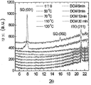
도 1a는 클로로포름으로부터 주조되고 다양한 온도에서 10분 동안 열적으로 어닐링된 SQ:PC70BM(1:6) 벌크 태양 전지, 및 클로로포름으로부터 주조되고 다양한 노출 시간 동안 디클로로메탄으로 용매 어닐링된 SQ:PC70BM(1:6) 벌크 태양 전지에 대한 XRD(X-선 회절 데이터)를 보여준다.
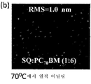
도 1b 내지 1d는 각각 클로로포름으로부터의 SQ:PC70BM(1:6) 벌크 태양 전지 생주물, 70℃에서 10분 동안 열적으로 어닐링된 SQ:PC70BM(1:6) 벌크 태양 전지, 및 12분 동안 디클로로메탄으로 용매 어닐링된 SQ:PC70BM(1:6) 벌크 태양 전지에 대한 RMS(제곱평균제곱근) 조도(roughness)를 보여준다.
도 2a는 클로로포름으로부터 주조되고 다양한 온도에서 열적으로 어닐링된 SQ:PC70BM(1:6) 벌크 태양 전지에 대한 FF 대 전력 강도를 보여준다.
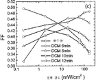
도 2b는 클로로포름으로부터 주조되고 다양한 노출 시간 동안 디클로로메탄으로 용매 어닐링된 SQ:PC70BM(1:6) 벌크 태양 전지에 대한 FF 대 전력 강도를 보여준다.
도 2c는 1,2-디클로로벤젠으로부터 주조되고 다양한 노출 시간 동안 디클로로메탄으로 용매 어닐링된 SQ:PC70BM(1:6) 벌크 태양 전지에 대한 FF 대 전력 강도를 보여준다.
도 3a는 1,2-디클로로벤젠으로부터 주조되고 다양한 노출 시간 동안 디클로로메탄으로 용매 어닐링된 SQ:PC70BM(1:6) 벌크 태양 전지에 대한 EQE를 보여준다.
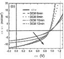
도 3b는 1,2-디클로로벤젠으로부터 주조되고 다양한 노출 시간 동안 디클로로메탄으로 용매 어닐링된 벌크 이종접합 소자에 대한 J-V를 보여준다.
도 3c는 1,2-디클로로벤젠으로부터 주조되고 다양한 노출 시간 동안 디클로로메탄으로 용매 어닐링된 벌크 이종접합 소자에 대한 ηΡ 대 전력 강도를 보여준다.
도 4는 DCB로부터 주조되고 다양한 노출 시간 동안 디클로로메탄으로 용매 어닐링된 SQ:PC70BM(1:6) 벌크 태양 전지에 대한 XRD를 보여준다.
도 5a 내지 5c는 각각 DCB로부터의 벌크 이종접합 소자 생주물, 12분 동안 디클로로메탄으로 용매 어닐링된 벌크 이종접합 소자, 및 30분 동안 디클로로메탄으로 용매 어닐링된 벌크 이종접합 소자의 RMS를 보여준다.
도 6a는 DCB로부터 주조되고 다양한 노출 시간 동안 디클로로메탄으로 용매 어닐링된 SQ:PC70BM(1:6) 벌크 태양 전지에 대한 흡수 계수를 보여준다.
도 6b는 DCB로부터 주조되고 다양한 노출 시간 동안 디클로로메탄으로 용매 어닐링된 SQ:PC70BM(1:6) 벌크 태양 전지에 대한 PL(광발광) 강도를 보여준다(도 6a 범례 참조).
도 6c는 DCB로부터 주조되고 다양한 노출 시간 동안 디클로로메탄으로 용매 어닐링된 SQ:PC70BM(1:6) 벌크 태양 전지에 대한 EQE를 보여준다(도 6a 범례 참조).
도 6d는 DCB로부터 주조되고 다양한 노출 시간 동안 디클로로메탄으로 용매 어닐링된 SQ:PC70BM(1:6) 벌크 태양 전지에 대한 전류 밀도 대 V(전압)를 보여준다(도 6a 범례 참조).
도 7a는 DCB로부터 주조되고 다양한 노출 시간 동안 디클로로메탄으로 용매 어닐링된 SQ:PC70BM(1:6) 벌크 태양 전지에 대한 ηΡ 대 전력 강도를 보여준다.
도 7b는 DCB로부터 주조되고 다양한 노출 시간 동안 디클로로메탄으로 용매 어닐링된 SQ:PC70BM(1:6) 벌크 태양 전지에 대한 FF 대 전력 강도를 보여준다.
도 8a는 다양한 온도에서 20분 동안 열적으로 어닐링된 여러 SQ:C60 평면 전지에 대한 XRD(X-선 회절) 데이터를 보여준다.
도 8b는 도 8a에서 시험된 평면 SQ:C60 소자에 대한 EQE를 보여준다.
도 9a는 도 8a에서 시험된 평면 SQ:C60 소자에 대한 ηΡ 대 전력 강도를 보여준다.
도 9b는 도 8에서 시험된 평면 SQ:C60 소자에 대한 FF 대 전력 강도를 보여준다.
도 10a는 DCB로부터 주조되고 다양한 온도에서 10분 동안 열적으로 어닐링된 여러 SQ:PC70BM(1:6) 벌크 이종접합 소자에 대한 XPS(X-선 광전자 분광법) 측정을 보여준다.
도 10b는 도 10a에 기재된 SQ:PC70BM(1:6) 벌크 이종접합 소자의 AFM(원자력 현미경) 측정을 보여준다.
도 11a는 도 10a에서 시험된 SQ:PC70BM(1:6) 벌크 이종접합 소자에 대한 ηΡ 대 전력 강도를 보여준다.
도 11b는 도 10a에서 시험된 SQ:PC70BM(1:6) 벌크 이종접합 소자에 대한 FF 대 전력 강도를 보여준다.
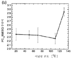
도 12a는 DCB로부터의 SQ:PC70BM(1:6) 벌크 이종접합 소자 생주물의 RMS(조도 측정 시스템)를 보여준다.
도 12b는 DCB로부터 주조된 후, 70℃에서 열적으로 어닐링된 SQ:PC70BM(1:6) 벌크 이종접합 소자의 RMS 조도를 보여준다.
도 12c는 DCB로부터 주조된 후, 30분 동안 디클로로메탄으로 용매 증기 어닐링되고 50℃에서 열적으로 어닐링된 SQ:PC70BM(1:6) 벌크 이종접합 소자의 RMS 조도를 보여준다.
도 12d는 DCB로부터 주조된 후, 110℃에서 열적으로 어닐링된 SQ:PC70BM(1:6) 벌크 이종접합 소자의 RMS 조도를 보여준다.
도 12e는 DCB로부터 주조된 후, 다양한 시간 동안 디클로로메탄으로 용매 증기 어닐링되고 50℃에서 열적으로 어닐링된 SQ:PC70BM(1:6) 벌크 이종접합 소자의 XRD 데이터를 보여준다.
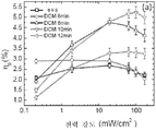
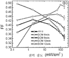
도 13a는 DCB로부터 주조된 후, 다양한 시간 동안 디클로로메탄으로 용매 증기 어닐링되고 50℃에서 열적으로 어닐링된 SQ:PC70BM(1:6) 벌크 이종접합 소자에 대한 ηΡ 대 전력 강도를 보여준다.
도 13b는 도 13a에서 시험된 SQ:PC70BM(1:6) 벌크 이종접합 소자에 대한 FF 대 전력 강도를 보여준다.
도 14는 도 13a에서 시험된 SQ:PC70BM(1:6) 벌크 이종접합 소자에 대한 EQE를 보여준다.
도 15는 주조되고 다양한 온도에서 열적으로 어닐링된 SQ/C60 평면 전지, 주조되고 다양한 온도에서 열적으로 어닐링된 SQ:PC70BM(1:6) 벌크 전지, 및 주조되고 1 태양 조명도(sun illumination)에서 2분, 6분, 8분 및 12분 동안 DCM 용매 어닐링된 SQ:PC70BM(1:6) 벌크 전지의 ηΡ 개요를 보여준다. BRIEF DESCRIPTION OF THE DRAWINGS The accompanying drawings, which are incorporated in and constitute a part of this specification, illustrate various embodiments of the invention and contribute to the description of the principles herein, as well as the detailed description. The drawings are not necessarily drawn to scale.
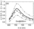
Figure 1a is cast from chloroform thermal annealing for 10 minutes at various temperatures SQ: PC 70 BM (1: 6) the bulk of the solar cell, and being cast from a chloroform solvent annealed with dichloromethane for various exposure times SQ: PC 70 XRD (X-ray diffraction data) for a BM (1: 6) bulk solar cell.
Figure 1b to 1d is SQ from each chloroform: PC 70 BM (1: 6 ) bulk solar cell production cast, annealed and thermally during the 70
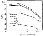
Figure 2a shows the FF versus power intensity for a SQ: PC 70 BM (1: 6) bulk solar cell cast from chloroform and thermally annealed at various temperatures.
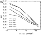
Figure 2b shows the FF versus power intensity for a SQ: PC 70 BM (1: 6) bulk solar cell cast from chloroform and solvent annealed with dichloromethane for various exposure times.
Figure 2c shows the FF versus power intensity for a SQ: PC 70 BM (1: 6) bulk solar cell cast from 1,2-dichlorobenzene and solvent annealed with dichloromethane for various exposure times.
Figure 3a shows the EQE for a SQ: PC 70 BM (1: 6) bulk solar cell cast from 1,2-dichlorobenzene and solvent annealed with dichloromethane for various exposure times.
Figure 3b shows the JV for a bulk heterojunction device cast from 1,2-dichlorobenzene and solvent annealed with dichloromethane for various exposure times.
Figure 3c shows the eta P vs. power intensity for a bulk heterojunction device cast from 1,2-dichlorobenzene and solvent annealed with dichloromethane for various exposure times.
Figure 4 shows the XRD for a SQ: PC 70 BM (1: 6) bulk solar cell cast from DCB and solvent annealed with dichloromethane for various exposure times.
5A-5C show the RMS of the bulk heterojunction element raw cast from DCB, the bulk heterojunction element solvent annealed with dichloromethane for 12 minutes, and the bulk heterojunction element solvent annealed with dichloromethane for 30 minutes.
Figure 6a shows the absorption coefficients for a SQ: PC 70 BM (1: 6) bulk solar cell cast from DCB and solvent annealed with dichloromethane for various exposure times.
Figure 6b shows the PL (photoluminescence) intensity for SQ: PC 70 BM (1: 6) bulk solar cell cast from DCB and solvent annealed with dichloromethane for various exposure times (see Figure 6a legend).
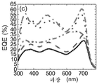
Figure 6c shows the EQE for a SQ: PC 70 BM (1: 6) bulk solar cell cast from DCB and solvent annealed with dichloromethane for various exposure times (see Figure 6a legend).
Figure 6d shows the current density versus V (voltage) for a SQ: PC 70 BM (1: 6) bulk solar cell cast from DCB and solvent annealed with dichloromethane for various exposure times (see Figure 6a legend).
Figure 7a shows the η Ρ power intensity for a SQ: PC 70 BM (1: 6) bulk solar cell cast from DCB and solvent annealed with dichloromethane for various exposure times.
Figure 7b shows the FF versus power intensity for a SQ: PC 70 BM (1: 6) bulk solar cell cast from DCB and solvent annealed with dichloromethane for various exposure times.
Figure 8a shows XRD (X-ray diffraction) data for several SQ: C 60 plane cells thermally annealed at various temperatures for 20 minutes.
Figure 8b is a plane SQ tested in Figure 8a: shows the EQE for C 60 element.
Figure 9a is a plane SQ tested in Figure 8a: shows an η Ρ high power intensity on the element C 60.
FIG. 9B shows the FF versus power intensity for the planar SQ: C 60 device tested in FIG.
Figure 10a shows XPS (X-ray photoelectron spectroscopy) measurements on various SQ: PC 70 BM (1: 6) bulk heterojunction devices cast from DCB and thermally annealed at various temperatures for 10 minutes.
Figure 10B shows AFM (atomic force microscope) measurements of the SQ: PC 70 BM (1: 6) bulk heterojunction device described in Figure 10a.
Figure 11a shows the η Ρ vs. power intensity for the SQ: PC 70 BM (1: 6) bulk heterojunction device tested in Figure 10a.
Figure 11B shows the FF versus power intensity for the SQ: PC 70 BM (1: 6) bulk heterojunction device tested in Figure 10a.
12A shows the RMS (illuminance measurement system) of a SQ: PC 70 BM (1: 6) bulk heterogeneous junction die cast from DCB.
Figure 12b shows the RMS illumination of the SQ: PC 70 BM (1: 6) bulk heterojunction device thermally annealed at 70 ° C after casting from DCB.
FIG. 12C shows the RMS illuminance of a SQ: PC 70 BM (1: 6) bulk heterojunction device solvent-vapor-annealed with dichloromethane for 30 minutes after being cast from DCB and thermally annealed at 50 ° C.
12D shows the RMS roughness of a SQ: PC 70 BM (1: 6) bulk heterojunction device thermally annealed at 110 ° C after being cast from DCB.
FIG. 12E shows XRD data of a SQ: PC 70 BM (1: 6) bulk heterojunction device solvent-vapor-annealed with dichloromethane for various times after being cast from DCB and thermally annealed at 50 ° C.
Figure 13a shows the eta P vs. power intensity for a SQ: PC 70 BM (1: 6) bulk heterojunction device solvent-vapor annealed with dichloromethane for various times after being cast from DCB and thermally annealed at 50 ° C.
Figure 13b shows the FF versus power strength for the SQ: PC 70 BM (1: 6) bulk heterojunction device tested in Figure 13a.
Figure 14 shows the EQE for the SQ: PC 70 BM (1: 6) bulk heterojunction device tested in Figure 13a.
Figure 15 shows a SQ / C 60 flat cell that is cast and thermally annealed at various temperatures, a SQ: PC 70 BM (1: 6) bulk cell that is cast and thermally annealed at various temperatures, illumination) in 2 minutes, 6 minutes, 8 minutes, and for 12 minutes, DCM solvent annealed SQ: PC 70 BM (1: 6) shows the outline of the bulk η Ρ cell.
정의Justice
본원에서 사용된 바와 같이, 용어 "유기"는 유기 광전자 소자의 제작에 사용될 수 있는 중합체 물질 및 소분자 유기 물질을 포함한다. "소분자"는 중합체가 아닌 임의의 유기 물질을 지칭하고, "소분자"는 실제로 꽤 클 수 있다. 소분자는 일부 환경 하에서 반복 유닛(unit)을 포함할 수 있다. 예를 들면, 장쇄 알킬 기를 치환기로서 사용하는 것은 "소분자" 부류로부터 분자를 배제하지 않는다. 소분자는 예를 들면, 중합체 골격 상의 펜던트(pendent) 기로서 또는 상기 골격의 일부로서 중합체 내로 도입될 수도 있다. 소분자는 코어 부분(moiety) 상에 구축된 일련의 화학적 외피(shell)로 구성된 덴드리머(dendrimer)의 코어 부분으로서 작용할 수도 있다. 덴드리머의 코어 부분은 형광 또는 인광 소분자 발광제(emitter)일 수 있다. 덴드리머는 "소분자"일 수 있다. 일반적으로, 소분자는 분자마다 동일한 분자량을 갖는 정의된 화학식을 갖는 반면, 중합체는 분자마다 상이할 수 있는 분자량을 갖는 정의된 화학식을 갖는다. 본원에서 사용된 바와 같이, "유기"는 하이드로카르빌과 헤테로원자로 치환된 하이드로카르빌 리간드의 금속 착물을 포함하나 이것으로 한정되지 않는다.As used herein, the term "organic" includes polymeric materials and small molecule organic materials that can be used in the fabrication of organic optoelectronic devices. "Small molecule" refers to any organic material that is not a polymer, and "small molecule" may actually be quite large. The small molecule may include a repeating unit under some circumstances. For example, using a long chain alkyl group as a substituent does not exclude molecules from the "small molecule" class. The small molecule may be introduced into the polymer, for example, as a pendent group on the polymer backbone or as part of the backbone. The small molecule may act as a core part of a dendrimer composed of a series of chemical shells built on a core moiety. The core portion of the dendrimer may be a fluorescent or phosphorescent small molecule emitter. The dendrimer may be a "small molecule ". Generally, a small molecule has a defined formula with the same molecular weight per molecule, while a polymer has a defined formula with a molecular weight that can vary from molecule to molecule. As used herein, "organic" includes, but is not limited to, a metal complex of a hydrocarbyl and a hydrocarbyl ligand substituted with a heteroatom.
벌크 이종접합 유기 광기전 전지의 제조 동안에 용매 어닐링, 구체적으로 용매 증기 어닐링 및 열적 어닐링을 이용하는 방법들 및 과정들이 본원에 기재되어 있다. 유기 물질의 형태 및 상 분리는 이들이 전하 분리 및 수집 둘다를 가능하게 한다는 점에서 중요할 수 있다. 본원에 기재된 용매 증기 어닐링 과정은 벌크 이종접합부를 포함하는 하나 이상의 유기 광활성 물질에 대한 템플레이팅(templating) 효과(이 효과는 정돈된 응집체를 형성하도록 유기 물질을 자가 조립시킴)를 나타내는 데에 유용할 수 있다. 유기 물질의 나노형태 및 결정도는 용매 종류 및 지속기간에 의존할 수 있다. 몇몇 실시양태에서, 본원에 기재된 용매 증기 어닐링 및/또는 열적 어닐링 과정은 성질 면에서 주로 비결정질 성질을 나타내는 생주물인 벌크 이종접합 블렌드를 포함하는 하나 이상의 유기 물질의 결정질 특징을 증가시킬 수 있다. Methods and processes for using solvent annealing, specifically solvent vapor annealing and thermal annealing, during the fabrication of bulk heterojunction organic photovoltaic cells are described herein. The morphology and phase separation of the organic material may be important in that they enable both charge separation and collection. The solvent vapor annealing process described herein is useful for indicating a templating effect on one or more organic photoactive materials comprising a bulk heterojunction (this effect self-assembling organic material to form ordered aggregates) . The nanostructure and crystallinity of the organic material may depend on the solvent type and duration. In some embodiments, the solvent vapor annealing and / or thermal annealing processes described herein can increase the crystalline character of one or more organic materials, including bulk heterogeneous blends, which are biomaterials that are predominantly amorphous in nature.
한 실시양태에서, 하기 단계를 포함하는, 감광성 소자의 제조 방법이 기재된다:In one embodiment, a method of making a photosensitive element is described comprising the steps of:
하나 이상의 전극 및 벌크 이종접합부를 포함하는 구조체를 제공하는 단계로서, 이때 상기 벌크 이종접합부가 하나 이상의 제1 유기 광활성 물질 및 하나 이상의 제2 유기 광활성 물질을 포함하는 것인 단계;Providing a structure comprising at least one electrode and a bulk heterojunction, wherein the bulk heterojunction comprises at least one first organic photoactive material and at least one second organic photoactive material;
하나 이상의 용매를 제공하는 단계;Providing at least one solvent;
상기 용매의 적어도 일부를 증기화시키는 단계; 및Vaporizing at least a portion of the solvent; And
상기 구조체의 적어도 일부를 증기화된 용매에 노출시키는 단계로서, 이때 상기 노출이 상기 제1 유기 광활성 물질 및 제2 유기 광활성 물질 중 하나 이상의 유기 광활성 물질의 결정도를 증가시키는 것인 단계. Exposing at least a portion of the structure to a vaporized solvent wherein the exposure increases the crystallinity of the at least one organic photoactive material of the first organic photoactive material and the second organic photoactive material.
몇몇 실시양태에서, 상기 방법은 상기 구조체를 열적으로 어닐링하는 단계를 더 포함한다. 몇몇 실시양태에서, 열적 어닐링 단계는 상기 구조체의 적어도 일부가 증기화된 용매에 노출된 후 일어난다. In some embodiments, the method further comprises thermally annealing the structure. In some embodiments, the thermal annealing step occurs after at least a portion of the structure is exposed to the vaporized solvent.
몇몇 실시양태에서, 상기 구조체는 하나 이상의 제1 유기 광활성 물질 및 하나 이상의 제2 유기 광활성 물질을 제1 전극 상에 증착시킴으로써 제조될 수 있다. 어닐링 과정이 완결된 후, 제2 전극은 벌크 이종접합부 상에서 패턴화될 수 있다.In some embodiments, the structure can be made by depositing one or more first organic photoactive material and at least one second organic photoactive material onto the first electrode. After the annealing process is complete, the second electrode may be patterned on the bulk heterojunction.
전극, 예컨대, 애노드(anode) 및 캐쏘드(cathode)는 금속 또는 "금속 대체물"로 구성될 수 있다. 여기서, 용어 "금속"은 원소적으로 순수한 금속으로 구성된 물질, 및 2개 이상의 원소적으로 순수한 금속으로 구성된 물질인 금속 합금 둘다를 포괄하기 위해 사용된다. 용어 "금속 대체물"은 통상의 정의 내에 있는 금속이 아니지만 금속 유사 성질, 예컨대, 전도성을 나타내는 물질을 지칭한다. 금속 대체물은 예를 들면, 도핑된 넓은 밴드갭(wide-bandgap) 반도체, 축퇴 반도체, 전도성 산화물 및 전도성 중합체를 포함한다. The electrodes, such as the anode and the cathode, may be composed of a metal or "metal substitute ". Here, the term "metal" is used to encompass both a material composed of an elementally pure metal and a metal alloy that is a material composed of two or more elementally pure metals. The term "metal substitute" refers to a material that is not a metal within the conventional definition, but exhibits metal-like properties, e.g., conductivity. Metal substitutes include, for example, doped wide-bandgap semiconductors, shrunken semiconductors, conductive oxides, and conducting polymers.
용어 "캐쏘드"는 하기 방식으로 사용된다. 주위 방사선조사 하에서 존재하고 저항 부하와 연결되어 있고 외부 인가된 전압, 예를 들면, PV 소자를 갖지 않은 비적층된 PV 소자 또는 적층된 PV 소자의 단일 유닛에서, 전자는 광전도성 물질로부터 캐쏘드로 이동한다. 유사하게, 용어 "애노드"는 조명 하에서 존재하는 PV 소자에서 정공이 반대 방식으로 이동하는 전자에 상응하여 광전도성 물질로부터 애노드로 이동하도록 본원에서 사용된다. 상기 용어들이 본원에서 사용된 바와 같이, 애노드 및 캐쏘드가 전극 또는 전하 전달 층일 수 있다는 것이 인식될 것이다.The term "cathode" is used in the following manner. In a single unit of a non-stacked PV element or stacked PV element that is present under ambient radiation and is connected to a resistive load and has no externally applied voltage, for example a PV element, the electrons move from the photoconductive material to the cathode do. Similarly, the term "anode" is used herein to move the photoconductive material from the photoconductive material to the anode corresponding to electrons moving in the opposite manner in the PV device present under illumination. It will be appreciated that, as the terms are used herein, the anode and cathode may be electrodes or charge transport layers.
전극은 단일 층 또는 다중 층("화합물" 전극)을 포함할 수 있고, 투명, 반투명 또는 불투명할 수 있다. 전극 및 전극 물질의 예로는 미국 특허 제6,352,777호(Bulovic et al.) 및 미국 특허 제6,420,031호(Parthasarathy, et al.)(이들 각각은 이들 각각의 특징의 개시내용에 대해 본원에 참고로 도입됨)에 개시된 전극 및 전극 물질이 있으나 이들로 한정되지 않는다. 본원에서 사용된 바와 같이, 층은 관련 파장에서 주위 전자기 방사선의 50% 이상을 투과시키는 경우 "투명"하다고 언급된다. The electrodes may comprise a single layer or multiple layers ("compound" electrodes) and may be transparent, translucent or opaque. Examples of electrodes and electrode materials are described in U.S. Patent No. 6,352,777 (Bulovic et al.) And U.S. Patent No. 6,420,031 (Parthasarathy, et al.), Each of which is incorporated herein by reference for the disclosure of their respective features , But are not limited thereto. As used herein, a layer is said to be "transparent" when transmitting at least 50% of ambient electromagnetic radiation at the wavelength of interest.
한 실시양태에서, 제1 전극은 산화몰리브데늄(MoOx)을 포함하는 계면 층을 포함할 수 있다. MoOx는 암전류를 감소시키고 개방 회로 전압을 증가시키는 데에 기여하는 것으로 생각되는, 유기 PV 전지 내의 예시적인 계면 층이다(Li, N. et al,. Open circuit voltage enhancement due to reduced dark current in small molecule photovoltaic cells, Appl. Phys. Lett., 94, 023307, Jan. 2009). In one embodiment, the first electrode may comprise an interfacial layer comprising molybdenum oxide (MoOx). MoOx is an exemplary interfacial layer in an organic PV cell that is believed to contribute to reducing dark current and increasing open circuit voltage (Li, N. et al., Open circuit voltage enhancement due to reduced dark current in small molecule photovoltaic cells, Appl. Phys. Lett., 94, 023307, Jan. 2009).
몇몇 실시양태에서, 제1 유기 광활성 물질은 공여체형 물질을 포함할 수 있다. 본원에서 사용될 수 있는 제1 유기 광활성 물질의 비한정적인 예로는 서브프탈로시아닌(SubPc), 구리 프탈로시아닌(CuPc), 클로로알루미늄 프탈로시아닌(CIAIPc), 주석 프탈로시아닌(SnPc), 펜타센, 테트라센, 디인데노페릴렌(DIP) 및 스쿠아레인(squaraine)(SQ)이 있다. In some embodiments, the first organic photoactive material may comprise a donor-type material. Non-limiting examples of the first organic photoactive material that can be used herein include, but are not limited to, subphthalocyanine (SubPc), copper phthalocyanine (CuPc), chloroaluminum phthalocyanine (CIAIPc), tin phthalocyanine (SnPc), pentacene, tetracene, Lilian (DIP) and squaraine (SQ).
몇몇 실시양태에서, 제2 유기 광활성 물질은 수용체형 물질을 포함할 수 있다. 본원에서 사용될 수 있는 제2 유기 광활성 물질의 비한정적인 예로는 C60, C70, [6,6]-페닐 C70 부티르산 메틸 에스테르(PC70BM), 3,4,9,10-페릴렌테트라카르복실릭비스-벤즈이미다졸(PTCBI) 및 헥사데카플루오로프탈로시아닌(F16CuPc)이 있다.In some embodiments, the second organic photoactive material may comprise a receptive material. Non-limiting examples of secondary organic photoactive materials that may be used herein include C 60 , C 70 , [6,6] -phenyl C 70 butyrate methyl ester (PC 70 BM), 3,4,9,10-perylene Tetracarboxylic bis-benzimidazole (PTCBI) and hexadecafluorophthalocyanine (F 16 CuPc).
또 다른 실시양태에서, 차단 층이 예컨대, 벌크 이종접합부와 제2 전극 사이에 포함될 수 있다. 여기자 차단 층(EBL)의 예는 미국 특허 제6,451,415호 및 제7,230,269호(Forrest et al.)(이들은 EBL에 관한 그들의 개시내용에 대해 본원에 참고로 도입됨)에 기재되어 있다. EBL의 추가 배경 설명은 문헌(Peumans et al., "Efficient photon harvesting at high optical intensities in ultrathin organic double-heterostructure photovoltaic diodes," Applied Physics Letters 76, 2650-52 (2000))(이 문헌도 본원에 참고로 도입됨)에서 찾을 수도 있다. EBL은 여기자가 공여체 및/또는 수용체 물질로부터 이동하여 나오는 것을 방지함으로써 소광(quenching)을 감소시키는 것으로 생각된다. 본원에서 사용될 수 있는 여기자 차단 층의 비한정적인 예로는 바쏘쿠프로인(BCP), 바쏘펜안쓰롤린(BPhen), 3,4,9,10-페릴렌테트라카르복실릭비스-벤즈이미다졸(PTCBI), 1,3,5-트리스(N-페닐벤즈이미다졸-2-일)벤젠((TPBi), 트리스(아세틸아세토네이토)루테늄(III)(RuAcaca3) 및 알루미늄(III)페놀레이트(Alq2 OPH)가 있다. In another embodiment, a barrier layer may be included, for example, between the bulk heterojunction and the second electrode. Examples of exciton barrier layers (EBL) are described in U.S. Patent Nos. 6,451,415 and 7,230,269 (Forrest et al.), Which are incorporated herein by reference for their disclosure of EBL. Further background information on EBL can be found in Peumans et al., "Efficient photon harvesting at high optical intensities in ultrathin organic double-heterostructure photovoltaic diodes," Applied Physics Letters 76, 2650-52 (2000) ). ≪ / RTI > The EBL is believed to reduce quenching by preventing excitons from migrating out of the donor and / or receptor material. Non-limiting examples of exciton blocking layers that may be used herein include, but are not limited to, bassocuproin (BCP), bassophene anthroline (BPhen), 3,4,9,10-perylenetetracarboxylic bis-benzimidazole PTCBI), 1,3,5-tris (N-phenylbenzimidazol-2-yl) benzene (TPBi), tris (acetylacetonato) ruthenium (III) Alq 2 OPH).
본원에서 사용될 수 있는 제2 전극의 예로는 금속 대체물, 비금속성 물질, 또는 예를 들면, Ag, Au 및 Al로부터 선택된 금속성 물질이 있다.Examples of second electrodes that can be used herein include metal substitutes, non-metallic materials, or metallic materials selected from, for example, Ag, Au and Al.
제1 전극이 전도성 산화물, 예컨대, 산화인듐주석(ITO), 산화주석(TO), 산화갈륨인듐주석(GITO), 산화아연(ZO) 및 산화아연인듐주석(ZITO)으로부터 선택된 전도성 산화물을 포함할 수 있고, 투명 전도성 중합체가 폴리아날린(PANI)을 포함한다는 것이 인식된다. 한 실시양태에서, 벌크 이종접합 유기 광기전 전지는 ITO/Mo03/SQ:PC70BM/LiF/Al; 및 ITO/Mo03/SQ:PC70BM/C60/BCP/LiF/Al를 포함한다. The first electrode comprises a conductive oxide selected from a conductive oxide such as indium tin oxide (ITO), tin oxide (TO), gallium indium tin oxide (GITO), zinc oxide (ZO) and zinc oxide indium tin , And that the transparent conductive polymer comprises polyaniline (PANI). In one embodiment, the bulk heterojunction organic photovoltaic cell comprises ITO / MoO 3 / SQ: PC 70 BM / LiF / Al; And ITO / MoO 3 / SQ: PC 70 BM / C 60 / BCP / LiF / Al.
본원에 기재된 유기 층의 두께는 25 내지 1200 Å, 예컨대, 50 내지 950 Å 또는 심지어 100 내지 700 Å일 수 있다.The thickness of the organic layer described herein may be from 25 to 1200 ANGSTROM, such as from 50 to 950 ANGSTROM or even from 100 to 700 ANGSTROM.
몇몇 실시양태에서, 벌크 이종접합부는 예를 들면, 진공 열적 증발(VTE), 회전 코팅 또는 유기 증기 상 증착(OVPD)에 의해 제조될 수 있다. OVPD는 OVPD가 운반체 기체를 사용하여 증기를 증착 챔버 내로 수송한다는 점에서 진공 열적 증발(VTE)과 상이하다. 증발 기능과 수송 기능의 공간적 분리는 증착 공정에 대한 정확한 조절, 및 유기 표면 형태, 예를 들면, 매끄러운 표면을 갖는 평면 또는 돌출부를 갖는 층에 대한 조절을 가능하게 한다.In some embodiments, the bulk heterojunction can be made, for example, by vacuum thermal evaporation (VTE), spin coating or organic vapor phase deposition (OVPD). OVPD differs from vacuum thermal evaporation (VTE) in that OVPD uses carrier gas to transport the vapor into the deposition chamber. Spatially separating the evaporative and transport functions enables precise control over the deposition process and control over layers with organic surface morphologies, such as planar or protruding portions, with smooth surfaces.
한 실시양태에서, 벌크 이종접합부는 회전 코팅에 의해 제조된다. 벌크 이종접합부를 회전 코팅을 통해 제조하는 경우, 상이한 용매 시스템의 사용은 완결 시 감광성 소자의 최종 효율에 영향을 미칠 수 있다. 예를 들면, 소자는 저비등점 온도를 갖는 용매 또는 고비등점을 갖는 용매에 의해 제조될 수 있다. 저비등점 용매는 신속히 증발되기 때문에, 고비등점 용매를 사용하여 형태를 더 조절하는 것이 바람직할 수 있다. 몇몇 실시양태에서, 벌크 이종접합부의 초기 제조에서 1,2-디클로로벤젠(DCB)과 같은 용매의 사용은 궁극적으로 저비등점 용매에 의해 제조된 PV 소자에 비해 용매 증기 어닐링 후 개선된 성능 성질을 나타내는 PV 소자를 발생시킬 수 있다.In one embodiment, the bulk heterojunction is made by spin coating. When bulk heterogeneous junctions are produced through spin coating, the use of different solvent systems can affect the final efficiency of the photosensitive element upon completion. For example, the device can be made with a solvent having a low boiling point temperature or a solvent having a high boiling point. Because the low boiling point solvent evaporates rapidly, it may be desirable to further regulate the form using a high boiling point solvent. In some embodiments, the use of a solvent such as 1,2-dichlorobenzene (DCB) in the initial preparation of bulk heterojunctions ultimately leads to improved performance properties after solvent vapor annealing compared to PV devices made by low boiling solvents A PV device can be generated.
몇몇 실시양태에서, 하나 이상의 제1 유기 광활성 물질 및 하나 이상의 제2 유기 광활성 물질은 1 atm에서 약 70℃ 이하의 비등점을 갖는 주조 용매로부터 주조된다. 예시적인 용매는 클로로포름을 포함할 수 있다. 또 다른 실시양태에서, 하나 이상의 제1 유기 광활성 물질 및 하나 이상의 제2 유기 광활성 물질은 1 atm에서 약 130℃ 보다 큰 비등점을 갖는 주조 용매로부터 주조된다. 또 다른 실시양태에서, 하나 이상의 제1 유기 광활성 물질 및 하나 이상의 제2 유기 광활성 물질은 1 atm에서 약 175℃ 보다 큰 비등점을 갖는 주조 용매로부터 주조된다. 예시적인 용매는 DCB를 포함할 수 있다.In some embodiments, the at least one first organic photoactive material and the at least one second organic photoactive material are cast from a casting solvent having a boiling point of less than about 70 占 폚 at 1 atm. Exemplary solvents may include chloroform. In another embodiment, the at least one first organic photoactive material and the at least one second organic photoactive material are cast from a casting solvent having a boiling point greater than about 130 캜 at 1 atm. In another embodiment, the at least one first organic photoactive material and the at least one second organic photoactive material are cast from a casting solvent having a boiling point greater than about 175 캜 at 1 atm. Exemplary solvents may include DCB.
벌크 이종접합 PV 전지의 특성을 개선하기 위해, 하나 이상의 유기 광활성 물질을 용매 증기 어닐링에 노출시킴으로써 증착된 유기 층의 막 형태를 더 최적화할 수 있다. 몇몇 실시양태에서, 하나 이상의 용매를 사용하여 최적 어닐링을 달성할 수 있다. 노출 시간은 유기 물질의 최종 형태에도 영향을 미칠 수 있다.In order to improve the properties of bulk heterojunction PV cells, the film morphology of the deposited organic layers can be further optimized by exposing one or more organic photoactive materials to solvent vapor annealing. In some embodiments, one or more solvents can be used to achieve optimal annealing. The exposure time can also affect the final form of the organic material.
예시적인 증기화 용매는 디클로로메탄이다. 몇몇 실시양태에서, 상기 구조체를 밀폐된 용기 내에서 증기화된 용매에 노출시키는 것이 바람직할 수 있다. 몇몇 실시양태에서, 상기 구조체를 약 5분 내지 약 30분 이상, 예컨대, 6분 내지 약 15분 또는 심지어 약 10분 내지 약 12분의 시간 동안 증기화된 용매에 노출시킬 수 있다.An exemplary vaporization solvent is dichloromethane. In some embodiments, it may be desirable to expose the structure to a vaporized solvent in a closed vessel. In some embodiments, the structure may be exposed to the vaporized solvent for a time of from about 5 minutes to about 30 minutes or more, such as from 6 minutes to about 15 minutes, or even from about 10 minutes to about 12 minutes.
몇몇 실시양태에서, 이종접합부를 열적 어닐링에 더 노출시키는 것도 바람직할 수 있다. 열적 어닐링 단계는 제조된 소자의 형태, 결정도 및/또는 향상된 성능을 더 조절하는 데에 도움이 될 수 있다. 예를 들면, 생주물 소자를 용매 증기 어닐링에 노출시킨 후 구조체를 열적으로 어닐링하는 것이 바람직할 수 있다. 열적 어닐링은 증기 어닐링 단계로부터 임의의 남아있는 용매를 제거하기에 충분한 온도에서 일어날 수 있다. 예를 들면, 상기 구조체를 디클로로메탄에 의한 용매 증기 어닐링에 노출시킨 후, 열을 상기 구조체에 직접적으로 인가함으로써 소자를 열적으로 어닐링하는 것이 바람직할 수 있다. 이것은 상기 구조체를 N2 대기 하에서 50℃까지 가열된 열판(hotplate) 상에 배치함으로써 달성될 수 있다. In some embodiments, it may be desirable to further expose the heterogeneous junction to thermal annealing. The thermal annealing step may help further control the shape, crystallinity and / or improved performance of the fabricated device. For example, it may be desirable to thermally anneal the structure after exposing the raw cast element to solvent vapor annealing. Thermal annealing may occur at a temperature sufficient to remove any remaining solvent from the vapor annealing step. For example, it may be desirable to thermally anneal the device by exposing the structure to solvent vapor annealing with dichloromethane followed by direct application of heat to the structure. This can be achieved by placing the structures on a heated hotplate (hotplate) under N 2 atmosphere to 50 ℃.
감광성 소자에서 하나 이상의 제1 유기 광활성 물질 및 하나 이상의 제2 유기 광활성 물질을 포함하는 벌크 이종접합부의 결정도를 향상시키는 방법도 본원에 기재된다. 이 실시양태에서, 상기 방법은 상기 벌크 이종접합부의 적어도 일부를 증기화된 용매에 노출시키는 단계를 포함하고, 이때 상기 감광성 소자는 상기 증기화된 용매에 노출되지 않은 소자에 비해 하나 이상의 하기 특성을 나타낸다:Methods of enhancing the crystallinity of bulk heterojoints comprising at least one first organic photoactive material and at least one second organic photoactive material in a photosensitive device are also described herein. In this embodiment, the method comprises exposing at least a portion of the bulk heterojunction to a vaporized solvent, wherein the photosensitive element has one or more of the following characteristics in comparison to an element that is not exposed to the vaporized solvent: Indicates:
증가된 충전율(FF); Increased charge rate (FF);
증가된 외부 양자 효율(EQE); 및Increased external quantum efficiency (EQE); And
증가된 전류 밀도 대 전압(J-V).Increased current density vs. voltage (J-V).
몇몇 실시양태에서, 상기 방법은 상기 구조체를 열적으로 어닐링하는 단계를 더 포함한다. 몇몇 실시양태에서, 열적 어닐링 단계는 상기 구조체의 적어도 일부가 상기 증기화된 용매에 노출된 후 일어난다. In some embodiments, the method further comprises thermally annealing the structure. In some embodiments, the thermal annealing step occurs after at least a portion of the structure is exposed to the vaporized solvent.
적합한 방법 및 물질은 하기에 상세히 논의된 방법 및 물질을 포함하나 이들로 한정되지 않는다.Suitable methods and materials include, but are not limited to, the methods and materials discussed in detail below.
실시예Example
본 개시내용은 예시적인 실시양태 및 실시예의 하기 상세한 설명을 참조함으로써 보다 용이하게 이해될 수 있다. 본 명세서에 개시된 설명 및 실시예에 비추어 볼 때 다른 실시양태들이 당업자에게 자명해질 것이라는 것이 이해된다. The present disclosure may be more readily understood by reference to the following detailed description of exemplary embodiments and examples. It is to be understood that other embodiments will become apparent to those skilled in the art in light of the description and embodiments disclosed herein.
실시예Example 1 One
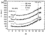
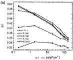
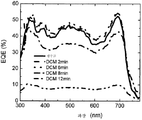
80 Å MoO3에 의해 예비코팅된 산화인듐주석(ITO) 기판 상에서 6000 RPM(분당 회전)의 속도로 회전 코팅된 SQ:PC70BM(1:6의 중량 농도) 박막의 X-선 회절(XRD) 패턴을, 40 kV Cu Kα 방사선 공급원을 이용하는 리가쿠(Rigaku) 회절계를 이용하여 θ-2θ 기하학적 구조로 수득하였다. 울람(Woolam) VASE 타원편광분석기(ellipsometer)를 이용하여 측정하였을 때, 클로로포름 중의 20 mg/㎖ 용액으로부터 주조된 SQ:PC70BM(1:6) 블렌드의 두께는 680 Å이었다.X-ray diffraction (XRD) of SQ: PC 70 BM (weight concentration of 1: 6) thin film spin coated on indium tin oxide (ITO) substrate pre-coated with 80 Å MoO 3 at a rate of 6000 RPM ) Pattern was obtained with a? -2? Geometry using a Rigaku diffractometer using a 40 kV Cu K ? Radiation source. When measured using a Woolam VASE ellipsometer, the thickness of the SQ: PC 70 BM (1: 6) blend cast from a 20 mg / ml solution in chloroform was 680 Å.
원자력 현미경(AFM) 이미지를 나노스코프(Noanoscope) III AFM에서 탭핑(tapping) 모드로 수집하였다. 용매 어닐링 샘플을 위해, SQ:PC70BM(1:6) 벌크 막을 1 ㎖의 디클로로메탄(DCM)으로 충전된 밀폐된 유리 바이알 내에서 6분 내지 30분의 시간 동안 후속 어닐링하였다. 열적 어닐링 샘플을 위해, SQ:PC70BM(1:6) 막을 50℃, 70℃, 110℃ 및 130℃에서 N2 장갑상자 내의 열판 상에서 10분 동안 어닐링하였다.Atomic Force Microscopy (AFM) images were collected in tapping mode on a Noanoscope III AFM. For the solvent annealing sample, the SQ: PC 70 BM (1: 6) bulk membrane was subsequently annealed in a sealed glass vial filled with 1 ml of dichloromethane (DCM) for a period of 6 minutes to 30 minutes. For the thermal annealing samples, SQ: PC 70 BM (1: 6) films were annealed for 10 minutes on hot plates in N 2 gloves at 50 캜, 70 캜, 110 캜 and 130 캜.
그 다음, (클로로포름 용매로부터의) 생주물 SQ:PC70BM(1:6) 막의 DCM 용매 어닐링을 하기 구조체를 갖는 태양 전지에 대해 수행하였다: ITO/MoO3(80 Å) /SQ:PC70BM(1:6 680 Å)/LiF(8 Å)/Al(1000 Å). 그 다음, 소자를 ITO/MoO3(80 Å)/SQ:PC70BM(1:6 680 Å)/C60(40 Å)/BCP(10 Å)/LiF(8 Å)/Al(1000 Å)로 구성된 구조체를 갖는 열적으로 증발된 C60 층으로 캡핑하였다. 그 다음, 10-7 토르의 기본 압력을 이용하여 MoO3을 진공 시스템 내에서 ITO 표면 상으로 열적으로 증발시켰다. 섀도 마스크(shadow mask)를 통해 8 Å LiF 및 1000 Å 두께의 Al 캐쏘드를 열적으로 증발시켜 7.9x10⁻³ ㎠의 소자 면적을 발생시킴으로써 소자 제조를 완결하였다. AM1.5G 필터 및 NREL 보정된 표준 Si 검출기를 갖는 Xe 아크 램프로부터의 오리엘(Oriel) 150 W 인공 태양(solar simulator) 방사선조사를 이용하여 상기 소자의 전류 밀도-전압(J-V) 특성 및 ηρ를 측정하였다. 표준 방법을 이용하여 측정 및 태양 분광 보정을 수행하였다. 400 Hz에서 단시간 차단되고 소자 활성 영역으로 집중되는 Xe 램프로부터의 단색 광을 이용하여 EQE를 측정하였다. DCM solvent annealing of the green cast SQ: PC 70 BM (1: 6) membrane (from chloroform solvent) was then performed on the solar cell with the following structure: ITO / MoO 3 (80 Å) / SQ: PC 70 BM (1: 6 680 Å) / LiF (8 Å) / Al (1000 Å). Next, the device was subjected to a thermal treatment using ITO / MoO 3 (80 Å) / SQ: PC 70 BM (1: 6 680 Å) / C 60 (40 Å) / BCP (10 Å) / LiF (8 Å) / Al ) it was in thermal capped with a C 60 evaporated layer having a structure configured. The MoO 3 was then thermally evaporated onto the ITO surface in a vacuum system using a base pressure of 10 -7 Torr. Device fabrication was completed by thermally evaporating 8 Å LiF and 1000 Å thick Al cathode through a shadow mask to generate a device area of 7.9 × 10 -3 ㎠. The current density-voltage (JV) characteristics and η ρ of the device using an Oriel 150 W solar simulator radiation from an Xe arc lamp with an AM1.5G filter and a NREL calibrated standard Si detector Were measured. Measurement and solar spectral correction were performed using standard methods. EQE was measured using monochromatic light from a Xe lamp, which was briefly blocked at 400 Hz and concentrated in the active area of the device.
도 1a에 나타낸 바와 같이, 50℃, 70℃, 110℃ 및 130℃에서 10분 동안 열적으로 어닐링된 SQ:PC70BM(1:6) 벌크 태양 전지에 대한 임의의 XRD 피크가 존재하는 것으로 보이지 않았는데, 이것은 비결정질 특징을 암시한다. 대조적으로, 12분보다 더 오랫동안 DCM 용매 어닐링을 수행한 후 (001) 및 (002) 피크로 잘 색인표시될 수 있는 SQ의 2개의 XRD 피크가 존재하는 것으로 보인다. 임의의 특정 이론에 구속받고자 하는 것은 아니지만, 용매 어닐링 후 SQ:PC70BM(1:6) 혼합물에서 SQ 피크는 상대적으로 약한 것으로 보이기 때문에, SQ가 정렬된/결정질 도메인을 형성하고, 이들 도메인 사이에 SQ 및 PC70BM의 비결정질 절편이 존재하는 것으로 생각된다. 생주물(도 1b) 및 4개의 열적으로 어닐링된 샘플들에 대한 AFM 이미지의 조도의 평균은 약 0.58 ± 0.12 nm이었고, SQ 상과 PC70BM 상의 명확한 상 분리 명암대조는 없는데, 이것은 XRD 측정 결과와 일치하는 것으로 보였다. PC70BM이 SQ 분자의 응집을 파괴할 수 있고 생주물 SQ:PC70BM 막에 대한 그의 결정도를 손상시킨다고 생각된다(도 1a). 대조적으로, 용매 어닐링 후 SQ:PC70BM 막의 조도는 약 0.58 ± 0.12 nm(생주물)부터 약 5.6 ± 1.2 nm까지 한 자릿수의 크기로 증가하는 것으로 보였다(8분 동안 DCM 어닐링 - 도 1c). 12분이라는 보다 긴 DCM 어닐링 시간은 SQ:PC70BM(1:6) 블렌드의 조도를 2배로 증가시키는 것으로 보였는데(도 1d), 이것은 보다 많은 SQ 덩어리(cluster)가 다결정으로 성장하기 시작할 때 발생된 보다 강한 상 분리를 암시한다. 따라서, 비결정질 생주물 SQ:PC70BM(1:6) 막의 DCM 어닐링이 SQ 상의 나노결정질 형태를 제공하였다고 생각된다. As shown in FIG. 1A, it appears that there is an arbitrary XRD peak for a SQ: PC 70 BM (1: 6) bulk solar cell thermally annealed at 50 ° C, 70 ° C, 110 ° C and 130 ° C for 10 minutes , Which suggests an amorphous character. In contrast, it appears that there are two XRD peaks of SQ that can be indexed well with the (001) and (002) peaks after DCM solvent annealing for longer than 12 minutes. While not wishing to be bound by any particular theory, it is believed that since the SQ peak appears to be relatively weak in the SQ: PC 70 BM (1: 6) mixture after solvent annealing, SQ forms an ordered / crystalline domain, It is believed that amorphous sections of SQ and PC 70 BM are present. The average of the roughness of the AFM image for the raw castings (FIG. 1 b) and the four thermally annealed samples was about 0.58 ± 0.12 nm, and there is no clear phase-contrast contrast contrast on the SQ and PC 70 BM, Respectively. It is believed that PC 70 BM is capable of destroying the aggregation of SQ molecules and impairing its crystallinity to the biomass SQ: PC 70 BM membrane (FIG. 1A). In contrast, after solvent annealing, the roughness of the SQ: PC 70 BM film appeared to increase by one order of magnitude from about 0.58 +/- 0.12 nm (raw cast) to about 5.6 +/- 1.2 nm (DCM annealing for 8 minutes - Figure 1c). The longer DCM annealing time of 12 min was seen to double the roughness of the SQ: PC 70 BM (1: 6) blend (Fig. 1d), which is the case when more SQ clusters begin to grow into polycrystals Suggesting stronger phase separation that occurred. Thus, it is believed that DCM annealing of the amorphous raw cast SQ: PC 70 BM (1: 6) film provided a nanocrystalline morphology on the SQ.
클로로포름 용매로부터의 SQ:PC70BM(1:6) 벌크 전지 생주물, 및 50℃ 내지 130℃의 온도에서 열적으로 어닐링된 SQ:PC70BM(1:6) 벌크 전지의 충전율은 도 2a에 나타나 있다. 열적 어닐링 과정은 충전율을 개선하는 것으로 보이지 않았는데, 이것은 도 1a의 XRD 데이터와 일치하였고, 열적 어닐링이 인지가능한 결정도 증가를 발생시킨다는 것을 암시하였다. DCM 용매 어닐링 과정 후, 클로로포름 용매로부터 주조된 SQ:PC70BM(1:6) 소자에 대한 결과는 도 2b에 나타나 있다. 나타낸 바와 같이, 1 태양 조명도에서 6분의 DCM 어닐링 시간을 이용하였을 때, 충전율의 개선이 있는 것으로 보인다. DCB 용매로부터 주조된 SQ:PC70BM(1:6) 소자(도 2c)에서, 충전율은 신속히 떨어지는 것으로 보인다. 대조적으로, 10분의 시간을 이용하였을 때, DCM 어닐링된 소자의 충전율은 1 태양 조명도에서 점진적으로 증가하는 것으로 보인다. 도 1a에 나타낸 바와 같이, DCM 용매 어닐링 시간의 보다 긴 지속은 블렌드에서 SQ 상의 결정도를 증가시키고, SQ:PC70BM(1:6) 블렌드에서 연장된 DCM 어닐링 시간은 충전율을 개선하는 것으로 보이는데, 이것은 적어도 부분적으로 SQ 상의 증가된 응집/결정질 함량에 기인하는 것으로 생각된다.From a chloroform solvent, SQ: in: (1-6) Fig. 2a the filling factor is the bulk cell PC 70 BM (1:: 6 ) Bulk cell production castings, and 50 ℃ is thermally annealed at a temperature of to 130 ℃ SQ PC 70 BM Is shown. The thermal annealing process did not appear to improve the fill rate, which was consistent with the XRD data in Figure 1A, suggesting that thermal annealing results in an increase in perceptible crystallinity. After DCM solvent annealing, the results for the SQ: PC 70 BM (1: 6) device cast from chloroform solvent are shown in FIG. 2b. As shown, there appears to be an improvement in the filling rate when using a DCM annealing time of 6 minutes in one solar light. In the SQ: PC 70 BM (1: 6) device (FIG. 2c) cast from DCB solvent, the charge rate appears to drop rapidly. In contrast, when using a time of 10 minutes, the charge rate of the DCM annealed device appears to increase gradually in 1 solar light. As shown in Figure 1A, a longer duration of DCM solvent annealing time increases the crystallinity on SQ in the blend, and the extended DCM annealing time in the SQ: PC 70 BM (1: 6) blend appears to improve the fill rate, This is believed to be due, at least in part, to increased aggregation / crystalline content on the SQ.
도 3a에서 DCB 용매로부터 주조된 생주물 및 용매 어닐링된 SQ:PC70BM(1:6) 벌크 전지의 외부 양자 효율(EQE)은 300 nm 내지 750 nm의 넓고 우수한 분광 반응을 암시한다. 약 λ=690 nm에서 존재하는 EQE 피크는 SQ 흡수에 기인하는 것으로 생각되는데, 이때 약 λ=350 nm 및 500 nm에서 집중된 피크는 PC70BM 흡수로부터 발생된 것으로 보인다. 10분의 DCM 용매 어닐링 시간을 이용하였을 때, 생성된 EQE 피크는 증가하고, 곡선 변동은 후속 DCM 용매 어닐링 과정 후 보다 더 균형을 이룬 여기자 해리 및 전하 수집을 암시한다. The external quantum efficiency (EQE) of the green cast and solvent annealed SQ: PC 70 BM (1: 6) bulk cell cast from DCB solvent in Figure 3a suggests a broad and excellent spectral response of 300 nm to 750 nm. The EQE peaks present at about lambda = 690 nm are believed to be due to SQ absorption, with peaks concentrated at about lambda = 350 nm and 500 nm appear to have originated from PC 70 BM absorption. When using a DCM solvent annealing time of 10 min, the resulting EQE peak is increased, and the curve variation implies more well-balanced exciton dissociation and charge collection after the subsequent DCM solvent annealing process.
1 태양 조명도에서 조명된, DCM 용매로부터 주조된 SQ:PC70BM(1:6) 벌크 전지의 J-V 특성은 도 3b에 나타나 있다. 후속 DCM 용매 어닐링은 단락 전류 밀도를 증가시키고 J-V 곡선의 형태를 변화시키는 것으로 보이는데, 이것은 상기 소자가 보다 높은 전도성을 나타내게 된다는 것을 암시한다. 10분의 DCM 어닐링을 이용하였을 때, SQ:PC70BM(1:6) 벌크 소자의 FF는 생주물 소자에 비해 보다 높은 전력 강도에서 상대적으로 보다 높은 값을 나타내는 것으로 보이는데, 이것은 벌크 막의 내부에서의 보다 우수한 운반체 전하 수송을 암시한다. 또한, 도 3c는 DCM 용매 어닐링된 소자가 ηP 대 전력 강도에서의 현저한 향상을 나타낸다는 것을 보여준다. 이들 결과는 도 2a 및 2b에 나타낸 열적 어닐링된 소자 및 용매 어닐링된 소자의 거동과 일치하는 것으로 보인다.The JV characteristics of a SQ: PC 70 BM (1: 6) bulk cell cast from a DCM solvent illuminated at 1 solar light are shown in FIG. 3b. Subsequent DCM solvent annealing appears to increase the short circuit current density and change the shape of the JV curve, suggesting that the device exhibits higher conductivity. The FF of the SQ: PC 70 BM (1: 6) bulk device appears to have a relatively higher value at higher power intensities compared to the biomedical device when using 10 min of DCM annealing, Lt; RTI ID = 0.0 > carrier < / RTI > Figure 3c also shows that the DCM solvent annealed element exhibits a significant improvement in < RTI ID = 0.0 > eta < / RTI > These results appear consistent with the behavior of the thermally annealed element and the solvent annealed element shown in Figs. 2A and 2B.
실시예Example 2 2
80 Å MoO3에 의해 예비코팅된 산화인듐주석(ITO) 코팅된 유리 기판 상에서 1000 RPM(분당 회전)의 낮은 속도로 30초 동안 회전 코팅된 SQ:PC70BM(1:6의 상대적 중량 농도) 박막의 X-선 회절(XRD) 패턴을, 40 kV Cu Kα 방사선 공급원을 이용하는 리가쿠 회절계를 이용하여 θ-2θ 기하학적 구조로 수득하였다. 울람 VASE 타원편광분석기를 이용하여 측정하였을 때, 열판 상에서 12시간 동안 가열된 1,2-디클로로벤젠(DCM) 중의 42 mg/㎖ 용액으로부터 주조된 SQ:PC70BM(1:6) 블렌드의 두께는 780 Å이었다.SQ: PC 70 BM (relative weight concentration of 1: 6) coated on the indium tin oxide (ITO) coated glass substrate preliminarily coated with 80 Å MoO 3 for 30 seconds at a low speed of 1000 RPM (rotation per minute) The X-ray diffraction (XRD) pattern of the thin film was obtained with a θ-2θ geometry using a Rigaku diffractometer using a 40 kV Cu K α radiation source. The thickness of the SQ: PC 70 BM (1: 6) blend cast from a 42 mg / ml solution in 1,2-dichlorobenzene (DCM) heated on a hot plate for 12 hours when measured using an Ullam VASE ellipsometer Was 780 Å.
원자력 현미경(AFM) 이미지를 나노스코프 III AFM에서 탭핑 모드로 수집하였다. SQ:PC70BM(1:6) 증착된 막의 용매 어닐링을 1 ㎖의 디클로로메탄(DCM)으로 충전된 밀폐된 유리 바이알 내에서 6분 내지 30분의 시간 동안 수행하였다. 투과 전자 현미경(TEM) 연구를 위해, 80 Å MoO3에 의해 코팅된 ITO 기판 상의 SQ:PC70BM(1:6) 막을 탈이온화된(DI) 물에 1시간 동안 침지시켰다. 그 다음, MoO3을 물에 용해시키고, 유기 층을 DI 물의 표면 상에 부유시켰다. 그 다음, 생주물 및 용매 어닐링된 SQ:PC70BM(1:6) 막을 홀리(holy) 탄소 막에 의해 코팅된 Cu 격자 상으로 옮겼다. TEM 이미지를 200 kV JEOL 2010F 분석 전자 현미경을 이용하여 촬영하였다. Atomic Force Microscopy (AFM) images were collected in tapping mode in a NanoScope III AFM. Solvent annealing of SQ: PC 70 BM (1: 6) deposited films was carried out in a sealed glass vial filled with 1 ml of dichloromethane (DCM) for a period of 6 to 30 minutes. For transmission electron microscopy (TEM) studies, SQ: PC 70 BM (1: 6) membranes on ITO substrates coated with 80 Å MoO 3 were immersed in deionized (DI) water for 1 hour. The MoO 3 was then dissolved in water and the organic layer was floated on the surface of the DI water. The raw cast and solvent annealed SQ: PC 70 BM (1: 6) film was then transferred to a Cu lattice coated with a holy carbon film. TEM images were taken using a 200 kV JEOL 2010F analytical electron microscope.
석영 기판 상의 생주물 및 4개의 DCM 어닐링된 막의 흡수 스펙트럼을 퍼킨-엘머(Perkin-Elmer) 람다 1500 UV-NIR 분광계를 이용하여 측정하였다. 광발광(PL)을 λ=600 nm의 여기 파장을 이용하여 측정하였다. 태양 전지 구조체는 하기 구조체를 이용하였다: ITO/MoO3(80 Å)/SQ:PC70BM(1:6 780 Å)/C60(40 Å)/BCP(10 Å)/Al(1000 Å). 여기서, 10-7 토르의 기본 압력을 이용하여 MoO3을 진공 시스템 내에서 ITO 표면 상으로 열적으로 증발시켰다. 회전 주조 증착 및 용매 어닐링 후, 섀도 마스크를 통해 8 Å LiF 및 1000 Å 두께의 Al 캐쏘드를 열적으로 증발시켜 8x10⁻³ ㎠의 소자 면적을 발생시킴으로써 소자 제조를 완결하였다. AM1.5G 필터 및 NREL 보정된 표준 Si 검출기를 갖는 Xe 아크 램프로부터의 오리엘 150 W 인공 태양 방사선조사를 이용하여 상기 소자의 전류 밀도-전압(J-V) 특성 및 전력 전환 효율(ηρ)을 측정하였다. 표준 방법을 이용하여 측정 및 태양 분광 보정을 수행하였다. 200 Hz에서 단시간 차단되고 소자 활성 영역으로 집중되는 Xe 램프로부터의 단색 광을 이용하여 EQE를 측정하였다.The absorption spectra of the raw castings on the quartz substrate and the four DCM annealed films were measured using a Perkin-Elmer Lambda 1500 UV-NIR spectrometer. Photoluminescence (PL) was measured using an excitation wavelength of? = 600 nm. The solar cell structure used was the following structure: ITO / MoO 3 (80 Å) / SQ: PC 70 BM (1: 6 780 Å) / C 60 (40 Å) / BCP (10 Å) . Here, MoO 3 was thermally evaporated onto the ITO surface in a vacuum system using a base pressure of 10 -7 Torr. After spin cast deposition and solvent annealing, device fabrication was completed by thermally evaporating 8 Å LiF and 1000 Å thick Al cathodes through a shadow mask to generate a device area of 8 × 10 -3 ㎠. Measure the current density-voltage (JV) characteristics and power conversion efficiency (η ρ ) of the device using Oriel 150 W artificial solar radiation from an Xe arc lamp with AM1.5G filter and NREL calibrated standard Si detector Respectively. Measurement and solar spectral correction were performed using standard methods. EQE was measured using monochromatic light from a Xe lamp that was briefly shut off at 200 Hz and concentrated in the active area of the device.
SQ:PC70BM(1:6) 블렌드의 후속 어닐링은 실온에서 초고 순도의 질소로 충전된 장갑상자 내에 봉입된 밀폐된 유리 바이알 내에서 상기 막을 DCM 증기에 6분 내지 30분 동안 노출시키는 것을 필요로 하였다. 도 4에 나타낸 바와 같이, 증착된 SQ:PC70BM 막에 대한 X-선 회절(XRD) 피크의 결여는 비결정질 구조를 암시한다. 대조적으로, 10분 동안의 어닐링 후, 어닐링 시간이 30분까지 연장되었을 때 강도에서 증가하는 피크가 약 2θ=7.80 ± 0.08o에서 나타난다. 이 피크는 약 11.26 ± 0.16 Å의 분자간 간격에 상응하는 SQ의 (001) 반사이다. DCM에 30분 동안 노출된 후, (002) 반사에 상응하는 제2 피크가 나타나는데, 이것은 질서에서의 계속된 증가를 암시한다. 12분 및 30분 동안 어닐링된 블렌드에서 SQ의 평균 결정 크기는 쉐러(Scherrer) 방법을 이용하여 XRD 피크 확장으로부터 추론하였을 때 각각 2.0 ± 0.2 nm 및 51 ± 4 nm인 것으로 평가된다. Subsequent annealing of the SQ: PC 70 BM (1: 6) blend requires the film to be exposed to the DCM vapor for 6 to 30 minutes in a sealed glass vial enclosed in ultra-high purity nitrogen filled glove box at room temperature Respectively. As shown in Figure 4, the lack of X-ray diffraction (XRD) peaks for the deposited SQ: PC 70 BM film suggests an amorphous structure. In contrast, after annealing for 10 minutes, an increasing peak in intensity when the annealing time was extended to 30 minutes appears at about 2? = 7.80 + 0.08 o . This peak is a (001) reflection of SQ corresponding to an intermolecular spacing of about 11.26 +/- 0.16 Angstroms. After exposure to DCM for 30 minutes, a second peak corresponding to the (002) reflection appears, suggesting a continued increase in order. The average crystal size of the SQ in the annealed blends for 12 and 30 minutes was estimated to be 2.0 0.2 nm and 51 4 nm, respectively, when deduced from the XRD peak expansion using the Scherrer method.
생주물 막의 AFM 이미지(도 5a)로부터 수득된 제곱평균제곱근 조도는 약 0.8 ± 0.1 nm이다. 대조적으로, 12분 동안의 용매 어닐링 후 상기 블렌드의 조도는 약 8.4 ± 1.2 nm까지 증가하는데(도 5b), 이것은 혼합물에서의 SQ의 다결정질 성장으로 인한 상당한 조면화(roughening)를 암시한다. 30분이라는 훨씬 더 긴 어닐링 시간을 이용하였을 때, 12.0 ± 1.4 nm까지의 추가 조면화(도 5c)에 의해 암시되는 바와 같이 SQ와 PC70BM의 상 분리는 계속된다. 부분적으로 상 분리에 기인하는 것으로 생각되는 조면화는 투사 전자 현미경(TEM) 이미지(도 5c) 및 AFM에 의해 측정된 표면 상 이미지(도 5c의 삽입도)에서도 관찰되었다. XRD 선 확장으로부터 상기 인식되는 바와 같이, 평균 결정 도메인 크기도 조면화와 동시에 증가하는 것으로 보인다.The root mean square roughness obtained from the AFM image (FIG. 5A) of the green mold film is about 0.8 0.1 nm. In contrast, after solvent annealing for 12 minutes, the intensity of the blend increases to about 8.4 + 1.2 nm (Fig. 5b), suggesting considerable roughening due to polycrystalline growth of SQ in the mixture. When using a much longer annealing time of 30 minutes, phase separation of SQ and PC 70 BM continues, as suggested by additional roughening up to 12.0 ± 1.4 nm (FIG. 5c). The roughening thought to be due in part to phase separation was also observed in a projection electron microscope (TEM) image (Fig. 5C) and also in a superficial image measured by AFM (Fig. As seen from the XRD line expansion, the average crystal domain size also appears to increase at the same time as roughening.
석영 기판 상의 생주물 및 4개의 DCM 용매 어닐링된 SQ:PC70BM 블렌드 막에 대한 가시광선에서의 분광이 도 6a에 나타나 있다. 전체 관찰된 분광 범위 전체에서 SQ의 흡수 계수는 8분까지 어닐링 시간과 함께 증가하지만, 시간이 더 증가하였을 때, 상기 변화는 포화되게 되는 것으로 보인다. 또한, 결정질 블렌드 막(DCM 12분)이 λ=680 nm에서 비결정질 막의 흡수 피크보다 덜 현저한 흡수 피크를 갖는 것으로 보인다.The spectra in the visible light for the raw castings on the quartz substrate and the four DCM solvent annealed SQ: PC 70 BM blend membranes are shown in Figure 6a. The absorption coefficient of SQ throughout the entire observed spectral range increases with annealing time to 8 minutes, but it appears that this change is saturated when the time is further increased. Also, the crystalline blend film (
막의 광발광(PL) 강도는 광발생된 공여체 여기자로부터 수용체 분자로의 전하 전달의 존재 하에서 소광된다(도 6b). 따라서, SQ:PC70BM 블렌드에서의 효율적인 PL 소광은 계면의 거리, 즉 LD 내에서의 광발생으로 인한 효율적인 여기자 해리를 암시하다. 전술된 바와 같이, 관련 길이 크기는 SQ의 경우 1.6 nm이고 PC70BM의 경우 20 nm 내지 40 nm이다. 10분은 최대 PL 강도 소광을 발생시키는 것으로 보이고, 그 후 어닐링 시간이 더 증가하였을 때 소광이 감소한다. 임의의 특정 이론에 구속받고자 하는 것은 아니지만, 이것은 본 발명자들의 LD 및 평균 미소결정(crystallite) 크기 δ 값의 관점에서 이해될 수 있다. PL 소광은 대략 10분 내지 12분의 어닐링 후 LD~δ~2 nm일 때 가장 강한 것으로 보인다. 추가 어닐링은 δ>>LD인 어느 시점에서 결정으로서의 추가 상 분리의 개시를 유발시키는 것으로 보이므로, 여기자는 해리 이종계면으로 더 이상 효율적으로 수송되지 않는다.The photoluminescence (PL) intensity of the film is quenched in the presence of charge transfer from the photogenerated donor excitons to the acceptor molecule (Figure 6b). Thus, efficient PL extinction in the SQ: PC 70 BM blend suggests efficient exciton dissociation due to light generation at the interface distance, L D. As described above, the associated length size is 1.6 nm for SQ and 20 nm to 40 nm for PC 70 BM. 10 minutes appears to cause maximum PL intensity extinction, and then the extinction decreases when the annealing time is further increased. Without wishing to be bound by any particular theory, this can be understood in view of the inventors' L D and the average crystallite size delta value. PL extinction appears to be strongest at L D ~ δ ~ 2 nm after approximately 10 to 12 min of annealing. Since the additional annealing appears to induce the initiation of further phase separation as crystals at some point < RTI ID = 0.0 >#< / RTI > L D , the excitons are no longer efficiently transported to the dissociation interface.
도 6c에서 생주물 및 용매 어닐링된 태양 전지의 EQE는 λ=300 nm의 파장부터 λ=750 nm까지 걸쳐 있는 흡수 분광으로서 유사하게 넓은 분광 반응을 암시한다. SQ의 EQE 피크는 약 26 ± 2%(생주물)부터 약 60 ± 1%(10분 동안 어닐링됨)까지 증가한다. 12분 동안의 어닐링 후, 피크 EQE는 전체 파장 범위에 걸쳐 40% 미만까지 감소한다. 흡수에서 수득된 결과와 유사한 이들 결과는 전지 효율이 LD에 필적할만한 최적 크기를 갖는 미소결정 크기에 강하게 의존하므로 SQ와 PC70BM 사이의 해리 공여체/수용체 계면으로의 최대 여기자 확산을 유발한다는 것을 더 암시한다.The EQE of the green mold and solvent annealed solar cell in FIG. 6c suggests a similarly broad spectroscopic response as absorption spectra ranging from a wavelength of? = 300 nm to? = 750 nm. The EQE peak of SQ increases from about 26 2% (raw cast) to about 60 1% (annealed for 10 minutes). After annealing for 12 minutes, the peak EQE decreases to less than 40% over the entire wavelength range. These results, similar to those obtained with absorption, indicate that cell efficiency strongly depends on the size of the crystallites having an optimal size comparable to L D , leading to maximum exciton diffusion to the dissociation donor / acceptor interface between SQ and PC 70 BM More hints.
1 태양 조명도의 AM1.5G 인공 태양 방사 하에서 측정된 도 6d의 J-V 특성은은 단락 전류 밀도(JSC)가 약 6.9 mA/㎠(생주물)부터 약 12.0 mA/㎠(10분 동안의 용매 어닐링)까지 향상된 다음, DCM에 12분 동안 노출된 후 약 8.3 mA/㎠까지 감소한다는 것을 암시한다. FF 결과는 어닐링 시간에 대한 유사한 의존성을 나타내는데, 이것은 개선된 분자 팩킹을 갖는 결정질 유기 물질에 대해 예측되는 바와 같이, 연장된 질서가 직렬 저항을 감소시킨다는 것을 암시한다. 변형된 다이오드 방정식을 이용하여 정방향 J-V 곡선을 피팅하여 직렬 비저항 RSA를 수득하였다. 생주물 전지는 약 35.2 ± 1.0 Ω·㎠의 RSA를 갖고, 그 후 상기 RSA는 어닐링 시간이 12분일 때 약 5.0 ± 0.5 Ω·㎠까지 점진적으로 감소한다. 그러나, DCM 어닐링 시간의 추가 증가는 활성 층과 접촉부 사이의 핀홀(pinhole)의 밀도를 증가시켜 단축된 다이오드를 유발할 수 있는 것으로 생각된다.JV characteristics of the first aspect jomyeongdo AM1.5G Figure 6d measured under irradiation of artificial sun is the short circuit current density (J SC) is about 6.9 mA / ㎠ (raw casting) from a solvent anneal for about 12.0 mA / ㎠ (10 bun ) And then decreased to about 8.3 mA / cm < 2 > after exposure to DCM for 12 minutes. The FF result shows a similar dependence on the annealing time, which implies that the extended order reduces the series resistance, as expected for crystalline organic materials with improved molecular packing. A series resistivity R SA was obtained by fitting a forward JV curve using a modified diode equation. The green cell has an R SA of about 35.2 ± 1.0 Ω ·
도 7a에 나타낸 바와 같이, 어닐링에 대한 광학적 변화 및 전기적 변화는 ηP를 증가시키는 것으로 보인다. 여기서, 생주물 전지의 ηP는 전력 강도와 함께 약간 증가하는 것으로 보인 후, 1 태양 조명도에서 약 2.4 ± 0.1%까지 차츰 감소하는 것으로 보이고, 이와 동시에 FF는 약 0.40 ± 0.02(0.002 태양 조명도)부터 약 0.36 ± 0.01(1 태양 조명도)까지 감소한다(도 7b 참조). 대조적으로, 10분 동안 어닐링된 전지의 경우, FF는 약 0.42 ± 0.01(0.002 태양 조명도)부터 약 0.50 ± 0.01(1 태양 조명도)까지 증가하고, 이 증가 동안 ηP는 1.5 ± 0.1%부터 5.2 ± 0.3%(1 태양 조명도)까지 상응하게 증가하는 것으로 보이고, 이때 이 집단 내의 전지에 대한 피크 측정된 값은 5.5%이다(JSC=2.0 mA/㎠, FF=0.5 및 VOC=0.92 V). 마지막으로, 12분 동안 어닐링된 전지는 ηP에서의 약 3.2 ± 0.1%의 감소를 보이는데, 이것은 감소된 EQE 및 FF에 기인할 수 있다.As shown in FIG. 7A, the optical change and the electrical change for annealing seem to increase? P. Here, the η P of the green cell showed a slight increase with the power intensity, then decreased gradually to about 2.4 ± 0.1% in 1 solar light, while at the same time the FF was about 0.40 ± 0.02 (0.002 solar light) To about 0.36 + -0.01 (1 solar illumination degree) (see Fig. 7B). In contrast, in the case of the annealing for 10 minutes, cells, FF is increased to about 0.42 ± 0.01 (0.002 lighting, road sun) of about 0.50 ± 0.01 from (1 sun lighting degrees) and for the increasing η P is from 1.5 ± 0.1% (J SC = 2.0 mA / cm < 2 >, FF = 0.5 and V OC = 0.92) for the cells in this population, V). Finally, the annealed cell for 12 minutes shows a reduction of about 3.2 +/- 0.1% at? P , which can be attributed to reduced EQE and FF.
실시예Example 3 3
이중층 구조체를 벌크 태양 전지와 비교하기 위해, SQ/C60 평면 전지를 대조군 전지로서 제작하였다. 소자 성능에 대한 결정도의 영향을 조사하기 위해, 생주물 SQ 박층을 50℃ 내지 130℃에서 어닐링하였다. 도 8a에 나타낸 바와 같이, 110℃ 및 130℃에서 어닐링된 SQ 막은 결정 특징을 암시하는 (001) 및 (002) 피크를 보인다. 평면 전지의 EQE(도 8b)는 110℃까지 증가된 어닐링 온도를 이용하였을 때 광반응이 개선된다는 것을 암시한다. 130℃의 어닐링 온도에서, SQ 막에 속하는 약 650 nm 및 약 750 nm의 2개 피크가 존재하는데, 이것은 단량체 SQ가 증가된 어닐링 온도를 이용하였을 때 이량체화 과정을 경험한다는 것을 암시한다. 110℃에서 어닐링된 전지는 1 태양 조명도에서 FF=0.59, VOC=0.76 V 및 JSC=10.05 mA/㎠와 함께 약 4.6%의 효율(ηP)을 나타내는 피크를 보이고, FF는 보다 낮은 강도에서 약 0.70에 가깝게 상승한다. 약 130℃까지 증가된 어닐링 온도를 이용하였을 때, ηP는 VOC가 0.46 V까지 떨어지기 때문에 2.9%까지 떨어지는 것으로 보인다(도 9a 및 9b 참조). 도 8a에 나타낸 바와 같이 130℃의 어닐링 온도를 이용하였을 때, 결정도는 증가하고 FF는 보다 높은 전력 강도에서 0.67까지 상승하는 것으로 생각된다. To compare the bilayer structure to the bulk solar cell, a SQ / C 60 flat cell was fabricated as a control cell. To investigate the effect of crystallinity on device performance, a thin layer of the green cast SQ was annealed at 50 캜 to 130 캜. As shown in FIG. 8A, the SQ films annealed at 110 캜 and 130 캜 show (001) and (002) peaks suggesting crystal characteristics. EQE (FIG. 8B) of the planar cell suggests that the photoreaction is improved when an increased annealing temperature is used up to 110 < 0 > C. At an annealing temperature of 130 캜, there are two peaks at about 650 nm and about 750 nm belonging to the SQ film, suggesting that monomer SQ experiences a dimerization process when using an increased annealing temperature. The cell annealed at 110 ° C shows a peak showing efficiency (η P ) of about 4.6% with FF = 0.59, V OC = 0.76 V and J SC = 10.05 mA /
SQ:PC70BM(1:6) 벌크 이종접합부를 실시예 2에 기재된 방식과 유사한 방식으로 제조하였다. 50℃, 70℃, 110℃ 및 130℃에서 10분 동안 어닐링된 SQ:PC70BM(1:6) 벌크 태양 전지에 대한 XRD 피크는 없는데, 이것은 비결정질 특징을 암시한다. 임의의 특정 이론에 구속받고자 하는 것은 아니지만, PC70BM은 SQ 분자의 응집을 파괴하고 그의 결정도를 손상시키는 것으로 생각된다. 생주물 및 4개의 열적으로 어닐링된 샘플에 대한 AFM 이미지의 조도의 평균은 약 0.579 ± 0.06 nm이고, SQ 상과 PC70BM 상의 명확한 상 분리 명암대조는 없는데, 이것은 XRD 측정 결과와 일치한다. 또한, 열적 어닐링을 통한 SQ 및 PC70BM의 성분 재조직화를 XPS로 조사한다(도 10). PC70BM 분자(C82H1402) 내에 N 원자가 존재하지 않기 때문에 402 eV의 결합 에너지를 갖는 N 1s 피크는 SQ:PC70BM 막의 상부 표면 상에서의 SQ(C32H44N2O6) 응집의 존재를 암시한다. SQ 및 PC70BM에 속하는 것으로 보이는 C 1s 및 O 1s의 강한 피크가 존재한다. 5개의 샘플에 대한 표면 상의 SQ 및 PC70BM의 조성을 XPS 측정으로부터 수득된 O/C 원자비를 이용하여 평가한다(도 10a). N 피크는 너무 약하기 때문에, C/N 또는 O/N 원자비는 상기 조성의 확인을 위해 적용되지 않는다. 도 10b에 나타낸 바와 같이, 다양한 SQ:PC70BM 샘플 표면으로부터 수득된 농도는 AFM 측정과 일치하고, 열적 어닐링 후 현저한 중량비 변화는 없다. 따라서, XRD, AFM 및 XPS 측정으로부터, 열적 가공만을 통한 회전 주조 샘플에서의 형태 또는 결정도 변화가 존재하는 것으로 보이지 않는다. SQ: PC 70 BM (1: 6) bulk heterogeneous junctions were prepared in a manner similar to that described in Example 2. There is no XRD peak for the SQ: PC 70 BM (1: 6) bulk solar cell annealed at 50 ° C, 70 ° C, 110 ° C and 130 ° C for 10 minutes, suggesting an amorphous character. While not intending to be bound by any particular theory, it is believed that PC 70 BM destroys the aggregation of SQ molecules and impairs its crystallinity. The mean of the roughness of the AFM image for the raw castings and the four thermally annealed samples is about 0.579 ± 0.06 nm and there is no clear phase-contrast contrast contrast between the SQ phase and the PC 70 BM, which is consistent with the XRD measurement results. In addition, the component reorganization of SQ and PC 70 BM through thermal annealing is investigated by XPS (FIG. 10). Because N atoms are absent in the PC 70 BM molecule (C 82 H 14 0 2 ), the
5개의 소자에 대한 소자 성능이 도 11에 나타나 있다. 70℃에서 어닐링된 SQ:PC70BM(1:6) 벌크 전지의 효율은 0.02 태양(2 mW/㎠) AM1.5G 조명도에서 약 5.3%(이때, FF=0.48)로부터 1 태양 조명도에서 약 4.0%(이때, FF=0.37)까지 떨어진다. FF의 하강은 이들 벌크 태양 전지가 저항성을 유지하고 각각의 전극으로의 이중-연속 전하 수송 경로의 결여(이것은 결과적으로 자유 운반체의 추출을 억제할 수 있음)를 나타낸다는 것을 암시한다.The device performance for the five devices is shown in Fig. The efficiency of a SQ: PC 70 BM (1: 6) bulk cell annealed at 70 ° C was about 5.3% (here, FF = 0.48) at 0.02 Sun (2 mW / % (At this time, FF = 0.37). The fall of FF implies that these bulk solar cells maintain resistivity and exhibit a lack of a double-continuous charge transport path to each electrode, which can consequently suppress the extraction of free carriers.
생주물 막에서 SQ 및 PC70BM의 형태 변화 및 결정도를 더 조절하기 위해, 용매 어닐링과 열적 어닐링의 조합을 조사하였다. 용매 어닐링 시간은 공기 중에서의 회전 코팅 직후 막을 덮어진 유리 병 내부에서 유지함으로써 조절된다. 상기 병을 1 ㎖ 디클로로메탄(DCM)으로 충전시킨다. 용매의 신속한 증발을 방지하기 위해, 상기 병을 덮개로 덮는다. 그 다음, 남아있는 DCM 용매를 제거하기 위해, 생주물 및 4개의 어닐링된 막을 N2 장갑상자 내의 열판 상에 놓아 50℃에서 어닐링하였다. 도 12에 나타낸 바와 같이, SQ:PC70BM 막의 조도는 약 0.83 nm(도 12a - 용매 또는 열적 어닐링을 이용하지 않은 생주물)부터 약 8.4 nm(도 12c - 30분 동안 DCM으로 용매 어닐링한 후, 50℃에서 열적으로 어닐링함)까지 한 자릿수의 크기로 증가한다. 도 12b 및 12d에 대한 결과는 열적 어닐링만에 대한 결과를 나타낸다. XRD 데이터(도 12e - 다양한 용매 어닐링 시간에 노출된 후 50℃에서 열적으로 어닐링된 막)는 보다 긴 시간 동안 어닐링된 SQ:PC70BM 막에 대한 (001) SQ 피크가 존재한다는 것을 명확히 보여주는데, 이것은 DCM 증기 상이 DCM 어닐링 용매의 가용성 및 휘발성을 통해 SQ:PC70BM 혼합물의 나노크기 상 분리를 촉진한다는 것을 암시한다. 결과는 SQ:PC70BM 벌크 태양 전지의 형태 및 분자 질서가 어닐링 용매의 가용성 및 증기압에 의해 조절될 수 있다는 것을 암시한다.In order to further control morphological change and crystallinity of SQ and PC 70 BM in the green cast film, the combination of solvent annealing and thermal annealing was investigated. The solvent annealing time is controlled by holding the film inside a covered glass bottle immediately after spin coating in air. The bottle is filled with 1 ml dichloromethane (DCM). In order to prevent rapid evaporation of the solvent, the bottle is covered with a cover. The green mold and the four annealed membranes were then placed on a hot plate in an N 2 glove box and annealed at 50 ° C to remove residual DCM solvent. As shown in Fig. 12, the roughness of the SQ: PC 70 BM film was about 8.4 nm (solvent densification without solvent or thermal annealing) about 0.83 nm (Fig. 12a - solvent annealing with DCM for 12 minutes Lt; RTI ID = 0.0 > 50 C). ≪ / RTI > The results for Figures 12b and 12d show the results for thermal annealing only. The XRD data (FIG. 12e - the film thermally annealed at 50 ° C after exposure to various solvent annealing times) clearly shows that there is a (001) SQ peak for annealed SQ: PC 70 BM film for a longer time, This suggests that the DCM vapor phase promotes nano-scale separation of the SQ: PC 70 BM mixture through the solubility and volatility of the DCM annealing solvent. The results suggest that the morphology and molecular order of the SQ: PC 70 BM bulk solar cell can be controlled by the solubility and vapor pressure of the annealing solvent.
다양한 시간 동안 DCM에 의한 용매 어닐링에 노출된 후 50℃에서 열적으로 어닐링된 소자의 성능은 도 13에 제시되어 있다. 0.02 태양 AM1.5G 조명도에서 6분 동안 어닐링된 샘플의 경우 약 5.3%의 가장 높은 효율(이때, FF=0.47)이 달성되고, 상기 효율은 1 태양 조명도에서 약 4.4%(이때, FF=0.39)까지 서서히 떨어진다. 6분 동안의 DCM 어닐링을 이용하였을 때, SQ:PC70BM 벌크 소자의 FF는 생주물 소자에 비해 보다 높은 전력 강도에서 보다 높은 값을 갖는 것으로 보이는데, 이것은 벌크 막의 내부에서의 보다 우수한 운반체 전하 수송을 암시한다. 상기 혼합물에서 SQ의 결정도 특징은 SQ 분자들이 정공 전하 수송을 향상시킬 수 있는 질서로 응집한다는 것을 암시한다. DCM 용매 어닐링은 열적 어닐링만으로부터의 소자 성능을 저하시키는 전하 불균형을 어느 정도 감소시키는 것으로 보인다. DCM으로 어닐링된 소자의 경우 FF가 0.50보다 여전히 낮기 때문에, SQ와 PC70BM 혼합물의 잘 조절된 나노크기의 상 분리를 다양한 용매 및 어닐링 시간을 통해 더 조사할 수 있다. 도 14는 약 300 nm 내지 약 750 nm의 분광 반응을 나타내는, 도 13에 기재된 제조된 소자의 EQE 반응을 보여준다.The performance of the device thermally annealed at < RTI ID = 0.0 > 50 C < / RTI > after exposure to solvent annealing by DCM for various times is shown in FIG. The highest efficiency (where FF = 0.47) of about 5.3% was achieved for a sample annealed for 6 minutes at 0.02 solar AM1.5G illumination and the efficiency was about 4.4% (where FF = 0.39) . When using DCM annealing for 6 min, the FF of the SQ: PC 70 BM bulk device appears to have a higher value at higher power intensities compared to the biomedical device, which leads to better carrier charge transport inside the bulk film . The crystallinity character of SQ in the mixture suggests that the SQ molecules aggregate into a system that can enhance hole charge transport. DCM solvent annealing appears to reduce the charge imbalance to some extent, which degrades device performance from thermal annealing only. Because the FF is still lower than 0.50 for devices annealed with DCM, well-regulated nano-sized phase separation of the SQ and PC 70 BM mixture can be further investigated through various solvents and annealing times. Figure 14 shows the EQE response of the fabricated device described in Figure 13, showing spectroscopic responses from about 300 nm to about 750 nm.
실시예 또는 달리 기재된 경우를 제외하고, 본 명세서 및 특허청구범위에서 사용된 성분의 양, 반응 조건, 분석 측정 등을 표현하는 모든 수치는 모든 경우 용어 "약"에 의해 수식되는 것으로 이해되어야 한다. 따라서, 반대로 기재되어 있지 않은 한, 본 명세서 및 첨부된 특허청구범위에 기재된 수치 파라미터는 본 개시내용으로 수득하고자 하는 원하는 성질에 따라 달라질 수 있는 근사치이다. 각각의 수치 파라미터는 적어도 특허청구범위에 대한 균등론의 적용을 한정하고자 하는 시도로서 해석되어서는 안 되고 유의한 아라비아 숫자의 수치 및 통상의 반올림법을 고려하여 해석되어야 한다. All numbers expressing quantities of ingredients, reaction conditions, analytical measurements and the like used in the specification and claims are to be understood as being modified in all instances by the term "about" unless otherwise stated or stated otherwise. Accordingly, unless indicated to the contrary, the numerical parameters set forth in this specification and the appended claims are approximations that may vary depending upon the desired properties sought to be obtained by this disclosure. Each numerical parameter should at least not be construed as an attempt to limit the application of the doctrine of equivalents to the claims, but should be construed in light of the significance of Arabic numerals and conventional rounding.
본 개시내용의 넓은 범위를 기재하는 수치 범위 및 파라미터가 근사치임에도 불구하고, 달리 기재되어 있지 않은 한, 구체적인 실시예에 기재된 수치 값은 가능한 정확하게 보고된다. 그러나, 임의의 수치 값은 그들의 각각의 시험 측정에서 발견된 표준 편차로부터 필수적으로 발생되는 일부 오차를 본질적으로 함유한다. Unless otherwise noted, the numerical values set forth in the specific examples are reported as precisely as possible, even though the numerical ranges and parameters setting forth the broad scope of the disclosure are approximations. However, any numerical value essentially contains some error that necessarily arises from the standard deviation found in their respective test measurements.
본원에서 사용된 바와 같이, 단수형 용어는 "하나 이상"을 의미하고, 명확히 반대로 기재되어 있지 않은 한, "하나만"으로 한정되어서는 안 된다. 따라서, 예를 들면, "층"은 "하나 이상의 층"을 의미하는 것으로 해석되어야 한다.As used herein, the singular terms mean "one or more ", and should not be limited to" one "unless explicitly stated to the contrary. Thus, for example, "layer" should be interpreted to mean "one or more layers ".
Claims (1)
하나 이상의 제1 전극 및 벌크 이종접합부(bulk heterojunction)를 보유하는 구조체를 제공하는 단계로서, 이때 상기 벌크 이종접합부가 하나 이상의 제1 유기 광활성 물질 및 하나 이상의 제2 유기 광활성 물질을 포함하는 것인 단계;
하나 이상의 용매를 제공하는 단계;
상기 용매의 적어도 일부를 증기화시키는 단계; 및
상기 구조체의 적어도 일부를 증기화된 용매에 노출시키는 단계로서, 이때 상기 증기화된 용매에의 노출이 상기 제1 유기 광활성 물질 및 제2 유기 광활성 물질 중 하나 이상의 유기 광활성 물질의 결정도를 증가시키는 것인 단계.A method for manufacturing a photosensitive device comprising the steps of:
Providing a structure having at least one first electrode and a bulk heterojunction, wherein the bulk heterojunction comprises at least one first organic photoactive material and at least one second organic photoactive material; ;
Providing at least one solvent;
Vaporizing at least a portion of the solvent; And
Exposing at least a portion of the structure to a vaporized solvent wherein exposure to the vaporized solvent increases the crystallinity of at least one of the first organic photoactive material and the second organic photoactive material In step.
Applications Claiming Priority (5)
| Application Number | Priority Date | Filing Date | Title |
|---|---|---|---|
| US32203910P | 2010-04-08 | 2010-04-08 | |
| US61/322,039 | 2010-04-08 | ||
| US39364610P | 2010-10-15 | 2010-10-15 | |
| US61/393,646 | 2010-10-15 | ||
| PCT/US2011/031439 WO2011127186A1 (en) | 2010-04-08 | 2011-04-06 | Enhanced bulk heterojunction devices prepared by thermal and solvent vapor annealing processes |
Related Parent Applications (1)
| Application Number | Title | Priority Date | Filing Date |
|---|---|---|---|
| KR1020127029251A Division KR20130094700A (en) | 2010-04-08 | 2011-04-06 | Enhanced bulk heterojunction devices prepared by thermal and solvent vapor annealing processes |
Related Child Applications (1)
| Application Number | Title | Priority Date | Filing Date |
|---|---|---|---|
| KR1020207029499A Division KR20200127032A (en) | 2010-04-08 | 2011-04-06 | Enhanced bulk heterojunction devices prepared by thermal and solvent vapor annealing processes |
Publications (1)
| Publication Number | Publication Date |
|---|---|
| KR20180108918A true KR20180108918A (en) | 2018-10-04 |
Family
ID=44201937
Family Applications (4)
| Application Number | Title | Priority Date | Filing Date |
|---|---|---|---|
| KR1020237013164A KR20230058180A (en) | 2010-04-08 | 2011-04-06 | Enhanced bulk heterojunction devices prepared by thermal and solvent vapor annealing processes |
| KR1020187027845A KR20180108918A (en) | 2010-04-08 | 2011-04-06 | Enhanced bulk heterojunction devices prepared by thermal and solvent vapor annealing processes |
| KR1020207029499A KR20200127032A (en) | 2010-04-08 | 2011-04-06 | Enhanced bulk heterojunction devices prepared by thermal and solvent vapor annealing processes |
| KR1020127029251A KR20130094700A (en) | 2010-04-08 | 2011-04-06 | Enhanced bulk heterojunction devices prepared by thermal and solvent vapor annealing processes |
Family Applications Before (1)
| Application Number | Title | Priority Date | Filing Date |
|---|---|---|---|
| KR1020237013164A KR20230058180A (en) | 2010-04-08 | 2011-04-06 | Enhanced bulk heterojunction devices prepared by thermal and solvent vapor annealing processes |
Family Applications After (2)
| Application Number | Title | Priority Date | Filing Date |
|---|---|---|---|
| KR1020207029499A KR20200127032A (en) | 2010-04-08 | 2011-04-06 | Enhanced bulk heterojunction devices prepared by thermal and solvent vapor annealing processes |
| KR1020127029251A KR20130094700A (en) | 2010-04-08 | 2011-04-06 | Enhanced bulk heterojunction devices prepared by thermal and solvent vapor annealing processes |
Country Status (9)
| Country | Link |
|---|---|
| US (1) | US9768402B2 (en) |
| EP (1) | EP2556548B1 (en) |
| JP (1) | JP5933524B2 (en) |
| KR (4) | KR20230058180A (en) |
| CN (1) | CN102939673B (en) |
| AU (1) | AU2011237636A1 (en) |
| CA (1) | CA2795742A1 (en) |
| TW (2) | TWI612683B (en) |
| WO (1) | WO2011127186A1 (en) |
Families Citing this family (10)
| Publication number | Priority date | Publication date | Assignee | Title |
|---|---|---|---|---|
| KR102063109B1 (en) * | 2012-07-11 | 2020-01-08 | 세메스 주식회사 | Substrate treating apparatus and substrate treating method |
| KR20150088830A (en) * | 2012-11-22 | 2015-08-03 | 더 리젠츠 오브 더 유니버시티 오브 미시간 | Use of inverse quasi-epitaxy to modify order during post-deposition processing or organic photovoltaics |
| CN103236503B (en) * | 2013-04-22 | 2015-07-01 | 国家纳米科学中心 | Polymer solar battery and preparation method thereof |
| JP6222229B2 (en) * | 2013-06-20 | 2017-11-01 | 日産化学工業株式会社 | Method for producing n-type organic semiconductor thin film |
| TW201501340A (en) * | 2013-06-27 | 2015-01-01 | Inst Nuclear Energy Res Atomic Energy Council | Method for manufacturing large-area organic solar cell |
| JP2015165529A (en) * | 2014-02-28 | 2015-09-17 | セイコーエプソン株式会社 | Method for manufacturing organic semiconductor film, organic semiconductor film, thin film transistor, active matrix device, electrooptical device and electronic apparatus |
| KR101515118B1 (en) * | 2014-03-12 | 2015-06-05 | 포항공과대학교 산학협력단 | Preparing method of vertically grown nanostructures of c60 and conjugated molecule |
| CN106816533B (en) * | 2017-03-09 | 2019-05-31 | 南京邮电大学 | A kind of inverse organic solar cell and preparation method thereof of phthalocyanine derivates film as cathode buffer layer |
| CN108807675A (en) * | 2018-05-07 | 2018-11-13 | 南京邮电大学 | A kind of preparation method of solar battery of surface passivation perovskite thin film |
| CN111628091A (en) * | 2020-06-08 | 2020-09-04 | 西北工业大学 | Method for improving quality of perovskite thin film through solvent bath auxiliary heat treatment |
Family Cites Families (21)
| Publication number | Priority date | Publication date | Assignee | Title |
|---|---|---|---|---|
| US6420031B1 (en) | 1997-11-03 | 2002-07-16 | The Trustees Of Princeton University | Highly transparent non-metallic cathodes |
| US6451415B1 (en) | 1998-08-19 | 2002-09-17 | The Trustees Of Princeton University | Organic photosensitive optoelectronic device with an exciton blocking layer |
| US6352777B1 (en) | 1998-08-19 | 2002-03-05 | The Trustees Of Princeton University | Organic photosensitive optoelectronic devices with transparent electrodes |
| WO2001017040A1 (en) * | 1999-08-31 | 2001-03-08 | E Ink Corporation | A solvent annealing process for forming a thin semiconductor film with advantageous properties |
| US7404862B2 (en) * | 2001-09-04 | 2008-07-29 | The Trustees Of Princeton University | Device and method for organic vapor jet deposition |
| US7306968B2 (en) * | 2002-09-05 | 2007-12-11 | Konarka Technologies, Inc. | Method for treating a photovoltaic active layer and organic photovoltaic element |
| US7829143B1 (en) * | 2003-11-21 | 2010-11-09 | Nanosolar, Inc. | Solvent vapor annealing of organic films |
| JP2005268449A (en) * | 2004-03-17 | 2005-09-29 | Asahi Kasei Corp | Method of reforming condensation polycyclic aromatic compound thin film, the compound thin film, and organic semiconductor device |
| US7194173B2 (en) * | 2004-07-16 | 2007-03-20 | The Trustees Of Princeton University | Organic devices having a fiber structure |
| US7375370B2 (en) * | 2004-08-05 | 2008-05-20 | The Trustees Of Princeton University | Stacked organic photosensitive devices |
| US8592680B2 (en) * | 2004-08-11 | 2013-11-26 | The Trustees Of Princeton University | Organic photosensitive devices |
| US7732229B2 (en) * | 2004-09-18 | 2010-06-08 | Nanosolar, Inc. | Formation of solar cells with conductive barrier layers and foil substrates |
| US7230269B2 (en) | 2005-06-13 | 2007-06-12 | The Trustees Of Princeton University | Organic photosensitive cells having a reciprocal-carrier exciton blocking layer |
| US20070290195A1 (en) * | 2005-08-22 | 2007-12-20 | Stephen Forrest | Increased open-circuit-voltage organic photosensitive devices |
| EP1929531B1 (en) * | 2005-08-25 | 2012-03-28 | Edward Sargent | Quantum dot optical devices with enhanced gain and sensitivity |
| JP2009090637A (en) * | 2007-09-18 | 2009-04-30 | Toppan Printing Co Ltd | Manufacturing process of organic function layer and organic functionality element and organic functionality element manufacturing equipment |
| EP2307483B1 (en) * | 2008-07-18 | 2015-04-22 | University Of Chicago | Semiconducting polymers |
| WO2010029542A1 (en) * | 2008-09-09 | 2010-03-18 | Technion Research & Development Foundation Ltd. | Derivatized fullerene-based dopants for organic semiconductors |
| US20100065112A1 (en) | 2008-09-15 | 2010-03-18 | Thompson Mark E | Organic Photosensitive Devices Comprising a Squaraine Containing Organoheterojunction and Methods of Making Same |
| CN101515631B (en) | 2009-03-24 | 2010-09-08 | 中国科学院长春应用化学研究所 | Method for preparing polymer solar cell |
| US8440496B2 (en) * | 2009-07-08 | 2013-05-14 | Solarmer Energy, Inc. | Solar cell with conductive material embedded substrate |
-
2011
- 2011-04-06 EP EP11717811.1A patent/EP2556548B1/en active Active
- 2011-04-06 KR KR1020237013164A patent/KR20230058180A/en not_active Application Discontinuation
- 2011-04-06 WO PCT/US2011/031439 patent/WO2011127186A1/en active Application Filing
- 2011-04-06 KR KR1020187027845A patent/KR20180108918A/en not_active Application Discontinuation
- 2011-04-06 US US13/080,759 patent/US9768402B2/en active Active
- 2011-04-06 KR KR1020207029499A patent/KR20200127032A/en not_active Application Discontinuation
- 2011-04-06 CN CN201180027965.4A patent/CN102939673B/en not_active Expired - Fee Related
- 2011-04-06 JP JP2013503916A patent/JP5933524B2/en active Active
- 2011-04-06 AU AU2011237636A patent/AU2011237636A1/en not_active Abandoned
- 2011-04-06 KR KR1020127029251A patent/KR20130094700A/en active Application Filing
- 2011-04-06 CA CA2795742A patent/CA2795742A1/en not_active Abandoned
- 2011-04-08 TW TW105142138A patent/TWI612683B/en active
- 2011-04-08 TW TW100112285A patent/TWI577035B/en active
Also Published As
| Publication number | Publication date |
|---|---|
| US9768402B2 (en) | 2017-09-19 |
| TWI577035B (en) | 2017-04-01 |
| CN102939673A (en) | 2013-02-20 |
| AU2011237636A1 (en) | 2012-11-08 |
| JP2013527978A (en) | 2013-07-04 |
| TW201210049A (en) | 2012-03-01 |
| KR20200127032A (en) | 2020-11-09 |
| EP2556548B1 (en) | 2022-02-23 |
| JP5933524B2 (en) | 2016-06-08 |
| CN102939673B (en) | 2018-05-15 |
| CA2795742A1 (en) | 2011-10-13 |
| US20130210189A1 (en) | 2013-08-15 |
| KR20130094700A (en) | 2013-08-26 |
| KR20230058180A (en) | 2023-05-02 |
| EP2556548A1 (en) | 2013-02-13 |
| WO2011127186A1 (en) | 2011-10-13 |
| TW201715739A (en) | 2017-05-01 |
| TWI612683B (en) | 2018-01-21 |
Similar Documents
| Publication | Publication Date | Title |
|---|---|---|
| TWI612683B (en) | Thermal and solvent vapor annealing processes for preparing a photosensitive device and enhancing the crystallinity of a bulk heterojunction comprised therein | |
| Kim et al. | Bulk heterojunction solar cells based on preformed polythiophene nanowires via solubility-induced crystallization | |
| KR101381523B1 (en) | Organic Photosensitive Cells Grown on Rough Electrode with Nano-Scale Morphology Control | |
| CA2562486C (en) | Method of fabricating an optoelectronic device having a bulk heterojunction | |
| US10263186B2 (en) | Bulk heterojunction organic photovoltaic cells made by glancing angle deposition | |
| Chen et al. | Chloroboron (III) subnaphthalocyanine as an electron donor in bulk heterojunction photovoltaic cells | |
| EP2875534A1 (en) | Multijunction organic photovoltaics incorporating solution and vacuum deposited active layers | |
| Ma et al. | Hybrid solar cells using solution-processed TiO2/Sb2S3 bilayer as electron transport layer | |
| Sun et al. | Scalable Solution‐Processed Hybrid Electron Transport Layers for Efficient All‐Perovskite Tandem Solar Modules | |
| Al-Shekaili et al. | Efficiency and stability improvement of organic solar cells based on PTB7: PCBM through hot-substrate coating | |
| Jin et al. | Hexadecafluorophthalocyaninatocopper as an electron conductor for high-efficiency fullerene-free planar perovskite solar cells | |
| Meiss et al. | Transparent electrode materials for solar cells | |
| AU2015224533A1 (en) | Enhanced bulk heterojunction devices prepared by thermal and solvent vapor annealing processes | |
| Das | Interfacial and Electrode Modifications in P 3 HT: PC 61 BM based Organic Solar Cells: Devices, Processing and Characterization | |
| Ying et al. | " Phase separation of co-evaporated ZnPc: C | |
| Salpeter | Optimization of material composition and processing parameters for hybrid organic-inorganic solar cells | |
| Lee et al. | Recent Progress toward High Efficiency Bulk Heterojunction Solar Cells | |
| EP2923390A2 (en) | Use of inverse quasi-epitaxy to modify order during post-deposition processing or organic photovoltaics |
Legal Events
| Date | Code | Title | Description |
|---|---|---|---|
| A107 | Divisional application of patent | ||
| E902 | Notification of reason for refusal | ||
| E601 | Decision to refuse application | ||
| J201 | Request for trial against refusal decision | ||
| J301 | Trial decision |
Free format text: TRIAL NUMBER: 2020101002509; TRIAL DECISION FOR APPEAL AGAINST DECISION TO DECLINE REFUSAL REQUESTED 20201014 Effective date: 20210615 |