KR20180098378A - Alternative target design for metrology using modulation technology - Google Patents
Alternative target design for metrology using modulation technology Download PDFInfo
- Publication number
- KR20180098378A KR20180098378A KR1020187021658A KR20187021658A KR20180098378A KR 20180098378 A KR20180098378 A KR 20180098378A KR 1020187021658 A KR1020187021658 A KR 1020187021658A KR 20187021658 A KR20187021658 A KR 20187021658A KR 20180098378 A KR20180098378 A KR 20180098378A
- Authority
- KR
- South Korea
- Prior art keywords
- target structure
- pattern
- substrate
- diffraction
- target
- Prior art date
- Legal status (The legal status is an assumption and is not a legal conclusion. Google has not performed a legal analysis and makes no representation as to the accuracy of the status listed.)
- Granted
Links
- 238000013461 design Methods 0.000 title description 8
- 239000000758 substrate Substances 0.000 claims abstract description 92
- 230000000737 periodic effect Effects 0.000 claims abstract description 9
- 238000000034 method Methods 0.000 claims description 56
- 230000003287 optical effect Effects 0.000 claims description 23
- 229920002120 photoresistant polymer Polymers 0.000 claims description 6
- 238000000059 patterning Methods 0.000 description 42
- 238000005286 illumination Methods 0.000 description 40
- 238000005259 measurement Methods 0.000 description 33
- 230000005855 radiation Effects 0.000 description 31
- 239000010410 layer Substances 0.000 description 23
- 210000001747 pupil Anatomy 0.000 description 14
- 230000004075 alteration Effects 0.000 description 12
- 238000003384 imaging method Methods 0.000 description 11
- 230000008569 process Effects 0.000 description 10
- 230000006870 function Effects 0.000 description 9
- 239000011295 pitch Substances 0.000 description 7
- 239000000047 product Substances 0.000 description 7
- 238000004519 manufacturing process Methods 0.000 description 6
- 238000001459 lithography Methods 0.000 description 5
- 238000001228 spectrum Methods 0.000 description 5
- 238000010586 diagram Methods 0.000 description 4
- 238000009826 distribution Methods 0.000 description 4
- 239000007788 liquid Substances 0.000 description 4
- 230000035945 sensitivity Effects 0.000 description 4
- 238000004590 computer program Methods 0.000 description 3
- 230000000694 effects Effects 0.000 description 3
- 238000007654 immersion Methods 0.000 description 3
- 239000002356 single layer Substances 0.000 description 3
- 239000002131 composite material Substances 0.000 description 2
- 238000001514 detection method Methods 0.000 description 2
- 239000011159 matrix material Substances 0.000 description 2
- 230000010363 phase shift Effects 0.000 description 2
- 238000012545 processing Methods 0.000 description 2
- 238000004088 simulation Methods 0.000 description 2
- 239000007787 solid Substances 0.000 description 2
- 230000003068 static effect Effects 0.000 description 2
- 238000003860 storage Methods 0.000 description 2
- 238000012546 transfer Methods 0.000 description 2
- 238000012935 Averaging Methods 0.000 description 1
- VYZAMTAEIAYCRO-UHFFFAOYSA-N Chromium Chemical compound [Cr] VYZAMTAEIAYCRO-UHFFFAOYSA-N 0.000 description 1
- XUIMIQQOPSSXEZ-UHFFFAOYSA-N Silicon Chemical compound [Si] XUIMIQQOPSSXEZ-UHFFFAOYSA-N 0.000 description 1
- 238000004458 analytical method Methods 0.000 description 1
- 238000013459 approach Methods 0.000 description 1
- 238000003491 array Methods 0.000 description 1
- 230000002238 attenuated effect Effects 0.000 description 1
- 239000006227 byproduct Substances 0.000 description 1
- 238000013500 data storage Methods 0.000 description 1
- 230000009977 dual effect Effects 0.000 description 1
- -1 e.g. Substances 0.000 description 1
- 238000001914 filtration Methods 0.000 description 1
- 238000007689 inspection Methods 0.000 description 1
- 239000002346 layers by function Substances 0.000 description 1
- 239000000463 material Substances 0.000 description 1
- 238000000691 measurement method Methods 0.000 description 1
- 230000007246 mechanism Effects 0.000 description 1
- QSHDDOUJBYECFT-UHFFFAOYSA-N mercury Chemical compound [Hg] QSHDDOUJBYECFT-UHFFFAOYSA-N 0.000 description 1
- 229910052753 mercury Inorganic materials 0.000 description 1
- 230000003278 mimic effect Effects 0.000 description 1
- 238000012986 modification Methods 0.000 description 1
- 230000004048 modification Effects 0.000 description 1
- 238000003909 pattern recognition Methods 0.000 description 1
- 230000010287 polarization Effects 0.000 description 1
- 238000000513 principal component analysis Methods 0.000 description 1
- 238000007639 printing Methods 0.000 description 1
- 238000004886 process control Methods 0.000 description 1
- 230000000644 propagated effect Effects 0.000 description 1
- 230000009467 reduction Effects 0.000 description 1
- 239000004065 semiconductor Substances 0.000 description 1
- 238000007493 shaping process Methods 0.000 description 1
- 229910052710 silicon Inorganic materials 0.000 description 1
- 239000010703 silicon Substances 0.000 description 1
- 238000012795 verification Methods 0.000 description 1
- XLYOFNOQVPJJNP-UHFFFAOYSA-N water Substances O XLYOFNOQVPJJNP-UHFFFAOYSA-N 0.000 description 1
- 229910052724 xenon Inorganic materials 0.000 description 1
- FHNFHKCVQCLJFQ-UHFFFAOYSA-N xenon atom Chemical compound [Xe] FHNFHKCVQCLJFQ-UHFFFAOYSA-N 0.000 description 1
Images


Classifications
-
- G—PHYSICS
- G03—PHOTOGRAPHY; CINEMATOGRAPHY; ANALOGOUS TECHNIQUES USING WAVES OTHER THAN OPTICAL WAVES; ELECTROGRAPHY; HOLOGRAPHY
- G03F—PHOTOMECHANICAL PRODUCTION OF TEXTURED OR PATTERNED SURFACES, e.g. FOR PRINTING, FOR PROCESSING OF SEMICONDUCTOR DEVICES; MATERIALS THEREFOR; ORIGINALS THEREFOR; APPARATUS SPECIALLY ADAPTED THEREFOR
- G03F7/00—Photomechanical, e.g. photolithographic, production of textured or patterned surfaces, e.g. printing surfaces; Materials therefor, e.g. comprising photoresists; Apparatus specially adapted therefor
- G03F7/70—Microphotolithographic exposure; Apparatus therefor
- G03F7/70483—Information management; Active and passive control; Testing; Wafer monitoring, e.g. pattern monitoring
- G03F7/70605—Workpiece metrology
- G03F7/70616—Monitoring the printed patterns
- G03F7/70633—Overlay, i.e. relative alignment between patterns printed by separate exposures in different layers, or in the same layer in multiple exposures or stitching
-
- G—PHYSICS
- G03—PHOTOGRAPHY; CINEMATOGRAPHY; ANALOGOUS TECHNIQUES USING WAVES OTHER THAN OPTICAL WAVES; ELECTROGRAPHY; HOLOGRAPHY
- G03F—PHOTOMECHANICAL PRODUCTION OF TEXTURED OR PATTERNED SURFACES, e.g. FOR PRINTING, FOR PROCESSING OF SEMICONDUCTOR DEVICES; MATERIALS THEREFOR; ORIGINALS THEREFOR; APPARATUS SPECIALLY ADAPTED THEREFOR
- G03F7/00—Photomechanical, e.g. photolithographic, production of textured or patterned surfaces, e.g. printing surfaces; Materials therefor, e.g. comprising photoresists; Apparatus specially adapted therefor
- G03F7/70—Microphotolithographic exposure; Apparatus therefor
- G03F7/70483—Information management; Active and passive control; Testing; Wafer monitoring, e.g. pattern monitoring
- G03F7/70605—Workpiece metrology
- G03F7/70681—Metrology strategies
- G03F7/70683—Mark designs
-
- G—PHYSICS
- G03—PHOTOGRAPHY; CINEMATOGRAPHY; ANALOGOUS TECHNIQUES USING WAVES OTHER THAN OPTICAL WAVES; ELECTROGRAPHY; HOLOGRAPHY
- G03F—PHOTOMECHANICAL PRODUCTION OF TEXTURED OR PATTERNED SURFACES, e.g. FOR PRINTING, FOR PROCESSING OF SEMICONDUCTOR DEVICES; MATERIALS THEREFOR; ORIGINALS THEREFOR; APPARATUS SPECIALLY ADAPTED THEREFOR
- G03F7/00—Photomechanical, e.g. photolithographic, production of textured or patterned surfaces, e.g. printing surfaces; Materials therefor, e.g. comprising photoresists; Apparatus specially adapted therefor
- G03F7/70—Microphotolithographic exposure; Apparatus therefor
- G03F7/70483—Information management; Active and passive control; Testing; Wafer monitoring, e.g. pattern monitoring
- G03F7/70605—Workpiece metrology
- G03F7/706843—Metrology apparatus
- G03F7/706845—Calibration, e.g. tool-to-tool calibration, beam alignment, spot position or focus
-
- G—PHYSICS
- G03—PHOTOGRAPHY; CINEMATOGRAPHY; ANALOGOUS TECHNIQUES USING WAVES OTHER THAN OPTICAL WAVES; ELECTROGRAPHY; HOLOGRAPHY
- G03F—PHOTOMECHANICAL PRODUCTION OF TEXTURED OR PATTERNED SURFACES, e.g. FOR PRINTING, FOR PROCESSING OF SEMICONDUCTOR DEVICES; MATERIALS THEREFOR; ORIGINALS THEREFOR; APPARATUS SPECIALLY ADAPTED THEREFOR
- G03F9/00—Registration or positioning of originals, masks, frames, photographic sheets or textured or patterned surfaces, e.g. automatically
- G03F9/70—Registration or positioning of originals, masks, frames, photographic sheets or textured or patterned surfaces, e.g. automatically for microlithography
- G03F9/7073—Alignment marks and their environment
- G03F9/7076—Mark details, e.g. phase grating mark, temporary mark
-
- G—PHYSICS
- G03—PHOTOGRAPHY; CINEMATOGRAPHY; ANALOGOUS TECHNIQUES USING WAVES OTHER THAN OPTICAL WAVES; ELECTROGRAPHY; HOLOGRAPHY
- G03F—PHOTOMECHANICAL PRODUCTION OF TEXTURED OR PATTERNED SURFACES, e.g. FOR PRINTING, FOR PROCESSING OF SEMICONDUCTOR DEVICES; MATERIALS THEREFOR; ORIGINALS THEREFOR; APPARATUS SPECIALLY ADAPTED THEREFOR
- G03F9/00—Registration or positioning of originals, masks, frames, photographic sheets or textured or patterned surfaces, e.g. automatically
- G03F9/70—Registration or positioning of originals, masks, frames, photographic sheets or textured or patterned surfaces, e.g. automatically for microlithography
- G03F9/7088—Alignment mark detection, e.g. TTR, TTL, off-axis detection, array detector, video detection
Landscapes
- Physics & Mathematics (AREA)
- General Physics & Mathematics (AREA)
- Engineering & Computer Science (AREA)
- Multimedia (AREA)
- Exposure And Positioning Against Photoresist Photosensitive Materials (AREA)
Abstract
본 명세서에서 타겟 구조가 개시되며, 상기 타겟 구조는 메트롤로지 툴로 측정되도록 구성되며, 상기 메트롤로지 툴은 회절 임계치를 갖고; 상기 타겟 구조는: 기판 상에 지지된 하나 이상의 패턴들을 포함하고, 상기 하나 이상의 패턴은 제 1 방향으로 제 1 주기로 주기적이고 제 2 방향으로 제 2 주기로 주기적이며, 상기 제 1 방향 및 제 2 방향은 상이하고 상기 기판에 평행하며, 상기 제 1 주기는 상기 회절 임계치와 동일하거나 그보다 크며, 상기 제 2주기는 상기 회절 임계치보다 작다. A target structure is disclosed herein wherein the target structure is configured to be measured with a metrology tool, the metrology tool having a diffraction threshold; The target structure comprising: at least one pattern supported on a substrate, the at least one pattern being periodic at a first period in a first direction and periodically at a second period in a second direction, the first and second directions being And the first period is equal to or greater than the diffraction threshold, and the second period is less than the diffraction threshold.
Description
본 출원은 2015년 12월 28일자로 출원된 미국 특허 출원 제 62/387,571 호의 우선권을 주장하며 그 전체가 참조로서 본 명세서에 포함된다. This application claims priority to U.S. Patent Application No. 62 / 387,571, filed December 28, 2015, which is incorporated herein by reference in its entirety.
본 발명은 회절 기반 광학을 사용하여 패턴의 오버레이 및 정렬을 측정하기 위한 타겟을 디자인하는 방법 및 장치에 관한 것이다.The present invention relates to a method and apparatus for designing a target for measuring overlay and alignment of a pattern using diffraction-based optics.
리소그래피 장치는 기판 상에, 통상적으로는 기판의 타겟부 상에 원하는 패턴을 적용시키는 기계이다. 리소그래피 장치는, 예를 들어 집적 회로(IC)의 제조 시에 사용될 수 있다. 그 경우, 대안적으로 마스크 또는 레티클이라 칭하는 패터닝 디바이스가 IC의 개별 층 상에 형성될 회로 패턴을 생성하기 위해 사용될 수 있다. 이 패턴은 기판(예컨대, 실리콘 웨이퍼) 상의 (예를 들어, 다이의 부분, 한 개 또는 수 개의 다이를 포함하는) 타겟부 상으로 전사(transfer)될 수 있다. 패턴의 전사는 통상적으로 기판 상에 제공된 방사선-감응재(레지스트)층 상으로의 이미징(imaging)을 통해 수행된다. 일반적으로, 단일 기판은 연속하여 패터닝되는 인접한 타겟부들의 네트워크를 포함할 것이다. 알려진 리소그래피 장치는, 한 번에 타겟부 상으로 전체 패턴을 노광함으로써 각각의 타겟부가 조사(irradiate)되는 소위 스테퍼, 및 방사선 빔을 통해 주어진 방향("스캐닝"-방향)으로 패턴을 스캐닝하는 한편, 이 방향과 평행한 방향(같은 방향으로 평행한 방향) 또는 역-평행 방향(반대 방향으로 평행한 방향)으로 기판을 동기적으로 스캐닝함으로써 각각의 타겟부가 조사되는 소위 스캐너를 포함한다. 또한, 기판 상에 패턴을 임프린트(imprint)함으로써 패터닝 디바이스로부터 기판으로 패턴을 전사할 수도 있다.A lithographic apparatus is a machine that applies a desired pattern onto a substrate, typically onto a target portion of the substrate. The lithographic apparatus may be used, for example, in the manufacture of integrated circuits (ICs). In that case, a patterning device, alternatively referred to as a mask or a reticle, may be used to generate a circuit pattern to be formed on an individual layer of the IC. This pattern can be transferred onto a target portion (e.g. comprising part of a die, including one or several dies) on a substrate (e.g. a silicon wafer). Transfer of the pattern is typically performed through imaging onto a layer of radiation-sensitive material (resist) provided on the substrate. In general, a single substrate will comprise a network of adjacent target portions that are successively patterned. Known lithographic apparatus include so-called steppers, in which each target portion is irradiated by exposing an entire pattern onto the target portion at one time, and scanning the pattern through a radiation beam in a given direction (the "scanning" -direction) Called scanner in which each target portion is irradiated by synchronously scanning the substrate in a direction parallel to this direction (parallel to the same direction) or in a reverse-parallel direction (parallel to the opposite direction). It is also possible to transfer the pattern from the patterning device to the substrate by imprinting the pattern on the substrate.
리소그래피 공정들에서는, 예를 들어 공정 제어 및 검증을 위해, 흔히 생성된 구조체들의 측정을 수행하는 것이 바람직하다. 이러한 측정들을 수행하는 다양한 툴들이 알려져 있으며, 임계 치수(CD)를 측정하는 데 흔히 사용되는 스캐닝 전자 현미경 및 오버레이, 즉 디바이스 내의 두 층들의 정렬 정확성을 측정하는 특수 툴들을 포함한다. 최근에는, 리소그래피 분야에서의 사용을 위해 다양한 형태의 스케터로미터(scatterometer)들이 개발되었다. 이 디바이스들은 타겟 상으로 방사선 빔을 지향하고, 산란된 방사선의 1 이상의 특성 - 예를 들어, 파장의 함수로서 단일 반사 각도에서의 세기; 반사된 각도의 함수로서 1 이상의 파장에서의 세기; 또는 반사된 각도의 함수로서 편광(polarization) - 을 측정하여, 타겟의 관심 특성이 결정될 수 있는 "스펙트럼"을 얻는다. 관심 특성의 결정은 다양한 기술들: 예를 들어, RCWA(rigorous coupled wave analysis) 또는 유한 요소 방법들; 라이브러리 탐색; 주성분 분석과 같은 반복 접근법들에 의한 타겟 구조체의 재구성에 의해 수행될 수 있다.In lithographic processes, for example, for process control and verification, it is often desirable to perform measurements of the resulting structures. Various tools for performing these measurements are known, and include a scanning electron microscope and overlay commonly used to measure critical dimensions (CD), i.e., special tools for measuring the alignment accuracy of the two layers in a device. In recent years, various types of scatterometers have been developed for use in the field of lithography. These devices direct the beam of radiation onto the target, and can measure at least one of the characteristics of the scattered radiation-for example, the intensity at a single angle of reflection as a function of wavelength; The intensity at one or more wavelengths as a function of the angle of reflection; Or polarization as a function of the angle of reflection - to obtain a "spectrum" from which the target's property of interest can be determined. Determination of the properties of interest may be accomplished by a variety of techniques including, for example, rigorous coupled wave analysis (RCWA) or finite element methods; Library navigation; And reconstruction of the target structure by iterative approaches such as principal component analysis.
몇몇 스케터로미터들에 의해 사용되는 타겟들은 비교적 큰 격자들, 예를 들어 40㎛×40㎛이며, 측정 빔은 격자보다 작은 스폿을 발생시킨다[즉, 격자가 언더필링(underfill)됨]. 이는 무한한 것으로서 간주될 수 있는 타겟의 수학적 재구성을 간소화한다. 하지만, 예를 들어 10㎛×10㎛ 이하까지 타겟들의 크기를 감소시켜서 이들이 스크라이브 레인(scribe lane)보다는 제품 피처(product feature)들 사이에 위치될 수 있기 위해, 격자가 측정 스폿보다 작게 만들어지는 메트롤로지가 제안되었다[즉, 격자가 오버필링(overfill)됨]. 통상적으로, 이러한 타겟들은 (정반사에 대응하는) 회절의 0차가 차단되고 고차들만이 처리되는 다크 필드 스캐터로메트리(dark field scatterometry)를 이용하여 측정된다.The targets used by some scatterometers are relatively large gratings, for example 40 占 퐉 x 40 占 퐉, and the measuring beam generates a spot smaller than the grating (i.e., the grating is underfilled). This simplifies the mathematical reconstruction of the target, which can be regarded as infinite. However, to reduce the size of the targets to, for example, 10 [mu] m x 10 [mu] m or less so that they can be positioned between product features rather than scribe lanes, A roll over is proposed (i.e., the grid is overfilled). Typically, such targets are measured using dark field scatterometry where the zeroth order of the diffraction (corresponding to specular reflection) is intercepted and only the higher orders are processed.
회절 차수들의 다크-필드 검출을 이용한 회절-기반 오버레이(DBO)는 더 작은 타겟들에 대한 오버레이 측정들을 가능하게 한다. 이 타겟들은 조명 스폿보다 작을 수 있고, 웨이퍼 상의 제품 구조체들에 의해 둘러싸일 수 있다. 하나의 이미지에서 다수 타겟들이 측정될 수 있다. 알려진 메트롤로지 기술에서, 오버레이 측정 결과들은 -1차 및 +1차 회절 세기들을 개별적으로 얻기 위해 조명 모드 또는 이미징 모드를 변화시키거나, 타겟을 회전시키면서, 소정 조건들 하에 타겟을 두 번 측정함으로써 얻어진다. 주어진 격자에 대한 이 세기들의 비교가 격자의 비대칭의 측정을 제공한다. Diffraction-based overlay (DBO) with dark-field detection of diffraction orders enables overlay measurements for smaller targets. These targets may be smaller than the illumination spot and may be surrounded by product structures on the wafer. Multiple targets in one image can be measured. In known metrology techniques, the overlay measurement results can be obtained by changing the illumination mode or the imaging mode to individually obtain the -1 st and +1 st diffracted intensities, or by measuring the target twice under certain conditions while rotating the target . A comparison of these intensities for a given lattice provides a measure of the asymmetry of the lattice.
리소그래피 장치, 레티클 및 프로세싱의 조합으로부터 발생하는 유효 노광 도즈는 전형적으로 중요한 제품 구조의 선 폭(임계 치수, CD)을 통해 측정된다. 이러한 측정에 사용되는 검사 장치에는 CD-SEM(Scanning Electron Microscope) 및 스 캐터로미터와 같은 메트롤로지 툴이 포함된다.Effective exposure doses resulting from a combination of lithographic apparatus, reticle, and processing are typically measured through line widths (critical dimension, CD) of critical product structures. Inspection devices used for these measurements include metrology tools such as CD-SEM (Scanning Electron Microscope) and scatterometers.
그러나, CD-SEM은 비교적 느리고 높은 잡음 레벨을 갖는다. 또한, 비록 스캐터로미터가 매우 민감한 메트롤로지 툴이지만, 리소그래피 장치(즉, 노광 시스템)의 수차는 디바이스 매칭 에러를 야기할 수 있다. 스캐터로메트리에 사용되는 현재의 메트롤로지 타겟은 가능한 서브-세그멘테이션 선 및/또는 공간이 있는 큰 피치(400-800 nm)에서 규칙적인 그레이팅으로 제한된다. 수차는 메트롤로지 타겟에서 물리적 시프트, 프로파일 비대칭 또는 세그먼트 비대칭을 야기할 수 있다. 일부 메모리 어플리케이션에서 선은 수평, 측면(lateral) 또는 회전 방향을 가질 수 있는 극 쌍극 조명(extreme dipole illumination) 하에서 인쇄된다. However, the CD-SEM has a relatively slow and high noise level. In addition, although the scatterometer is a very sensitive metrology tool, the aberration of the lithographic apparatus (i.e., the exposure system) can cause device matching errors. Current metrology targets used in scatterometry are limited to regular gratings at large pitches (400-800 nm) with possible sub-segmentation lines and / or space. The aberration can cause physical shift, profile asymmetry or segment asymmetry in the metrology target. In some memory applications, the lines are printed under extreme dipole illumination, which may have horizontal, lateral, or rotational directions.
이미지 수차 문제의 완화를 위하여, 조명 모드와 다른 프로세스 제약들에 호환되는 메트롤로지 타겟의 설계 단계에서 더 나은 제어가 요구된다.In order to alleviate the image aberration problem, better control is required in the design stage of the metrology target that is compatible with the illumination mode and other process constraints.
본 명세서에서 타겟 구조가 개시되며, 상기 타겟 구조는 메트롤로지 툴로 측정되도록 구성되며, 상기 메트롤로지 툴은 회절 임계치를 갖고; 상기 타겟 구조는: 기판 상에 지지된 하나 이상의 패턴들을 포함하고, 상기 하나 이상의 패턴은 제 1 방향으로 제 1 주기로 주기적이고 제 2 방향으로 제 2 주기로 주기적이며, 상기 제 1 방향 및 제 2 방향은 상이하고 상기 기판에 평행하며, 상기 제 1 주기는 상기 회절 임계치와 동일하거나 그보다 크며, 상기 제 2 주기는 상기 회절 임계치보다 작다. A target structure is disclosed herein wherein the target structure is configured to be measured with a metrology tool, the metrology tool having a diffraction threshold; The target structure comprising: at least one pattern supported on a substrate, the at least one pattern being periodic at a first period in a first direction and periodically at a second period in a second direction, the first and second directions being And the first period is equal to or greater than the diffraction threshold, and the second period is less than the diffraction threshold.
일 실시 예에 의하면, 상기 하나 이상의 패턴은 상기 제 1 차수보다 높은 회절 차수를 희생하면서 상기 제 1 방향으로 상기 타겟 구조로부터의 제 1 차 회절을 향상시키도록 구성된다. According to one embodiment, the at least one pattern is configured to enhance a first order diffraction from the target structure in the first direction, sacrificing a diffraction order higher than the first order.
일 실시 예에 의하면, 상기 하나 이상의 패턴은 상기 제 2 방향에서의 상기 타겟 구조로부터의 회절이 단지 0 차(zero-th)를 갖도록 구성된다.According to one embodiment, the at least one pattern is configured such that diffraction from the target structure in the second direction has only zero-th.
일 실시 예에 의하면, 상기 하나 이상의 패턴은 메트롤로지 툴이 하나 이상의 패턴으로부터 정렬 또는 오버레이를 측정할 수 있도록 구성된다.According to one embodiment, the one or more patterns are configured so that the metrology tool can measure alignment or overlay from one or more patterns.
일 실시 예에 의하면, 상기 하나 이상의 패턴은 포토 레지스트로 형성된다. According to one embodiment, the at least one pattern is formed of a photoresist.
일 실시 예에 의하면, 상기 하나 이상의 패턴은 상기 기판 내로 에칭된다. According to one embodiment, the at least one pattern is etched into the substrate.
일 실시 예에 의하면, 상기 하나 이상의 패턴은 상기 패턴을 둘러싸는 객체와는 상기 기판에 수직한 방향으로 상이한 높이를 갖는다.According to one embodiment, the at least one pattern has a different height in a direction perpendicular to the substrate than an object surrounding the pattern.
일 실시 예에 의하면, 상기 하나 이상의 패턴은 상기 패턴을 둘러싸는 객체와는 상이한 광학 특성을 갖는다. According to one embodiment, the at least one pattern has an optical characteristic different from an object surrounding the pattern.
일 실시 예에 의하면, 상기 제 1 방향은 상기 제 2 방향에 수직이다. According to one embodiment, the first direction is perpendicular to the second direction.
일 실시 예에 의하면, 상기 제 1 주기는 상기 제 1 방향 이외의 방향으로 상기 하나 이상의 패턴의 치수의 주기이다. According to one embodiment, the first period is a period of a dimension of the at least one pattern in a direction other than the first direction.
일 실시 예에 의하면, 상기 제 1 방향 이외의 방향으로 상기 하나 이상의 패턴의 치수는 상기 제 1 방향으로 상기 하나 이상의 패턴의 위치의 사인 함수이다. According to one embodiment, the dimension of the at least one pattern in a direction other than the first direction is a sine function of the position of the at least one pattern in the first direction.
일 실시 예에 의하면, 상기 하나 이상의 패턴은 상기 제 2 방향의 라인을 포함한다. According to one embodiment, the at least one pattern comprises a line in the second direction.
일 실시 예에 의하면, 상기 라인은 상기 제 1 방향으로 동일한 크기를 갖는다. According to one embodiment, the lines have the same size in the first direction.
일 실시 예에 의하면, 상기 라인 각각은 상기 제 1 방향으로 균일한 크기를 갖는다. According to one embodiment, each of the lines has a uniform size in the first direction.
본 명세서에서는 기판이 개시되며, 상술된 타겟 구조와 전자 디바이스의 구조를 나타내는 패턴을 포함한다. A substrate is disclosed herein and includes a pattern representing the structure of the electronic device and the target structure described above.
본 명세서에서는 상술된 타겟 구조를 제조하는 방법이 개시되며, 상기 방법은, 상기 기판 상에 복수의 평행한 라인을 제조하는 단계; 상기 라인의 길이를 변경함으로써 상기 하나 이상의 패턴들을 형성하는 단계를 포함한다. Disclosed herein is a method of making a target structure as described above, the method comprising: fabricating a plurality of parallel lines on the substrate; And forming the one or more patterns by varying the length of the lines.
일 실시 예에 의하면, 상기 라인을 제조하는 단계는 제 1 패터닝 디바이스로 노광하는 단계를 포함하고, 상기 패턴을 형성하는 단계는 제 2 패터닝 디바이스로 노광하는 단계를 포함한다. According to one embodiment, the step of fabricating the line includes exposing to a first patterning device, and the step of forming the pattern comprises exposing to a second patterning device.
본 명세서에서는 전자 디바이스의 2 개의 상이한 층 상의 구조 사이의 오버레이를 측정하는 컴퓨터 구현 방법이 개시되며, 상기 2 개의 층 각각은 타겟 구조를 포함하고, 상기 2 개의 층 상의 타겟 구조 중 하나 이상은 상술된 타겟 구조이며, 상기 방법은: 상기 타겟 구조로부터 회절 차수를 측정하는 단계; 상기 회절 차수로부터 오버레이 오차를 결정하는 단계를 포함한다. Disclosed herein is a computer-implemented method for measuring an overlay between structures on two different layers of an electronic device, each of the two layers comprising a target structure, Target structure, the method comprising: measuring a diffraction order from the target structure; And determining an overlay error from the diffraction order.
본 명세서에서는 기판 상에 존재하는 구조에 정렬시키는 컴퓨터 구현 방법이 개시되며, 상기 기판은 상술된 타겟 구조를 포함하며, 상기 방법은: 상기 타겟 구조로부터 회절 차수를 측정하는 단계; 상기 회절 차수로부터 정렬 오차를 결정하는 단계를 포함한다. Disclosed herein is a computer implemented method for aligning to a structure present on a substrate, the substrate comprising a target structure as described above, the method comprising: measuring a diffraction order from the target structure; And determining an alignment error from the diffraction order.
본 명세서에서는 전자 데이터가 저장된 컴퓨터 판독 가능 비-일시적인 매체가 개시되며, 상기 전자 데이터는 상술된 타겟 구조를 표현한다. Disclosed herein is a computer-readable non-transitory medium in which electronic data is stored, the electronic data representing the target structure described above.
본 명세서에서는 기판 상의 타겟 구조를 사용하여 정렬 또는 오버레이를 측정하는 방법이 개시되며, 상기 방법은, 상기 타겟 구조로부터 제 1 방향으로의 회절 차수를 측정하는 단계 - 상기 타겟 구조는 상기 제 1 차수보다 높은 회절 차수를 희생시키면서 상기 제 1 방향으로의 회절의 제 1 차수를 향상시키도록 구성되며, 상기 타겟 구조로부터 제 2 방향으로의 회절은 0 차 차수만을 가지며, 상기 제 1 방향 및 상기 제 2 방향은 상이하고 상기 기판에 평행함 -; 및 상기 제 1 방향의 회절 차수로부터 정렬 오차 또는 오버레이 오차를 결정하는 단계를 포함한다.There is disclosed herein a method of aligning or measuring an overlay using a target structure on a substrate, the method comprising the steps of measuring a diffraction order from the target structure in a first direction, Wherein the diffraction from the target structure in the second direction has only a zero order order and is configured to enhance the first order of diffraction in the first direction while sacrificing a high diffraction order, Is different and parallel to the substrate; And determining an alignment error or an overlay error from the diffraction order in the first direction.
일 실시 예에 의하면, 상기 제 1 차수보다 큰 상기 제 1 방향의 회절 차수는 상기 타겟 구조에 의해 향상되지 않는다.According to one embodiment, the diffraction order in the first direction greater than the first order is not improved by the target structure.
일 실시 예에 의하면, 상기 제 1 방향은 상기 제 2 방향에 수직이다. According to one embodiment, the first direction is perpendicular to the second direction.
일 실시 예에 의하면, 상기 타겟 구조는 하나 이상의 패턴을 포함하고, 상기 하나 이상의 패턴은 상기 제 1 방향으로의 제 1 주기로 주기적이고 상기 제 2 방향으로의 제 2 주기로 주기적이다. According to one embodiment, the target structure comprises at least one pattern, wherein the at least one pattern is periodic with a first period in the first direction and with a second period in the second direction.
일 실시 예에 의하면, 상기 제 1 주기는 상기 제 1 방향을 제외한 방향으로의 하나 이상의 패턴들의 치수의 주기이다. According to one embodiment, the first period is a period of a dimension of one or more patterns in a direction other than the first direction.
일 실시 예에 의하면, 상기 타겟 구조는 포토 레지스트로 형성된다. According to one embodiment, the target structure is formed of a photoresist.
일 실시 예에 의하면, 상기 타겟 구조는 상기 기판 내로 에칭된다. According to one embodiment, the target structure is etched into the substrate.
일 실시 예에 의하면, 상기 타겟 구조는 상기 제 2 방향의 라인을 포함한다. According to one embodiment, the target structure comprises a line in the second direction.
일 실시 예에 의하면, 상기 라인은 상기 제 1 방향으로 동일한 크기를 갖는다. According to one embodiment, the lines have the same size in the first direction.
일 실시 예에 의하면, 상기 라인 각각은 상기 제 1 방향으로 균일한 크기를 갖는다. According to one embodiment, each of the lines has a uniform size in the first direction.
명령들을 갖는 컴퓨터 판독 가능 비-일시적인 매체로서, 상기 명령들은, 컴퓨터에 의해 실행될 때, 상술된 방법을 구현한다. A computer readable non-volatile medium having instructions that, when executed by a computer, implement the method described above.
본 개시의 이들 및 다른 양태 및 특징은 첨부된 도면과 함께 본 개시의 특정 실시 예에 대한 다음의 설명을 검토하면 당업자에게 명백해질 것이다:
도 1은 본 개시의 일 실시 예에 따른 리소그래피 장치를 도시한다.
도 2 (a)는 제 1 쌍의 조명 어퍼처를 사용하는 실시 예에 따른 타겟을 측정하는데 사용하기위한 다크-필드 스캐터로미터의 개략도를 도시한다.
도 2 (b)는 주어진 조명 방향에 대한 타겟 격자의 회절 스펙트럼의 상세를 도시한다.
도 3은 공지된 형태의 다중 격자 타겟 및 기판 상의 측정 스폿의 아웃라인을 도시한다.
도 4는 도 2 (a)의 스캐터로미터에서 얻어진 도 3의 타겟의 이미지를 도시한다.
도 5a는 표준 격자의 단면도를 도시한다.
도 5b 내지 도 5d는 회절 기반 스캐터로메트리를 사용하여 2 개의 수직 층의 격자들 사이의 오버레이 측정의 원리를 도시한다.
도 6은 본 개시의 일 실시 예에 따른 곡선 격자 구조 및 기하학적 설계 파라미터를 도시한다.
도 7, 도 8, 도 9a 및 도 9b는 본 개시의 일 실시 예에 따른 2 개의 마스크를 사용하여 생성된 격자 구조를 도시한다.
도 10은 본 개시의 실시 예에 따른 완전(fully) 변조된 격자 구조의 다른 실시 예를 도시한다.
도 11은 본 개시의 실시 예에 따른, 솔리드 곡선 격자 구조 및 대응하는 기하학적 파라미터를 도시한다.
도 12는 본 개시에 따른, 변조된 기하학적 파라미터를 사용하여 메트롤로지 타겟을 설계하는 방법의 흐름도를 도시한다.These and other aspects and features of the present disclosure will become apparent to those skilled in the art upon examination of the following description of specific embodiments of the disclosure in conjunction with the accompanying drawings, wherein:
Figure 1 illustrates a lithographic apparatus according to one embodiment of the present disclosure.
Figure 2 (a) shows a schematic diagram of a dark-field scatterometer for use in measuring a target according to an embodiment using a first pair of illumination apertures.
Figure 2 (b) shows the details of the diffraction spectrum of the target grating for a given illumination direction.
Figure 3 shows the outline of a measurement spot on a substrate and a multiple lattice target of known type.
Figure 4 shows an image of the target of Figure 3 obtained in the scatterometer of Figure 2 (a).
Figure 5a shows a cross-sectional view of a standard grating.
Figures 5b to 5d illustrate the principle of overlay measurement between two vertical layer gratings using diffraction based scatterometry.
Figure 6 illustrates a curvilinear grating structure and geometric design parameters in accordance with one embodiment of the present disclosure.
Figures 7, 8, 9A, and 9B illustrate a lattice structure created using two masks according to one embodiment of the present disclosure.
Figure 10 shows another embodiment of a fully modulated lattice structure according to an embodiment of the present disclosure.
Figure 11 shows a solid curve lattice structure and corresponding geometric parameters, according to an embodiment of the present disclosure.
12 shows a flow diagram of a method for designing a metrology target using modulated geometric parameters according to the present disclosure.
본 명세서는 본 발명의 특징들을 구체화하는 1 이상의 실시 예들을 개시한다. 개시된 실시예(들)는 단지 본 발명을 예시한다. 개시된 실시예(들)에 본 발명의 범위가 제한되지는 않는다. 본 발명은 본 명세서에 첨부된 청구항들에 의해 정의된다.This specification discloses one or more embodiments that incorporate features of the invention. The disclosed embodiment (s) merely illustrate the present invention. The scope of the present invention is not limited to the disclosed embodiment (s). The invention is defined by the claims appended hereto.
본 명세서에서, "하나의 실시 예", "일 실시 예", "예시적인 실시 예" 등으로 설명된 실시 예(들) 및 이러한 언급들은, 설명된 실시 예(들)가 특정한 특징, 구조 또는 특성을 포함할 수 있지만, 모든 실시 예가 특정한 특징, 구조 또는 특성을 반드시 포함하는 것은 아닐 수 있음을 나타낸다. 또한, 이러한 어구들이 반드시 동일한 실시 예를 칭하는 것은 아니다. 또한, 특정한 특징, 구조 또는 특성이 일 실시 예와 관련하여 설명되는 경우, 다른 실시 예들과 관련하여 이러한 특징, 구조 또는 특성을 초래하는 것은 명확하게 설명되든지 그렇지 않든지 당업자의 지식 내에 있음을 이해한다.In the present specification, the embodiment (s) described in the context of "one embodiment", "one embodiment", "exemplary embodiment", and the like, Features, but it should be understood that not all embodiments necessarily include a particular feature, structure, or characteristic. Further, such phrases do not necessarily refer to the same embodiment. Furthermore, when a particular feature, structure, or characteristic is described in connection with an embodiment, it is to be understood that within the knowledge of one of ordinary skill in the art, which results in such feature, structure, .
본 발명의 실시 예들은 하드웨어, 펌웨어, 소프트웨어 또는 여하한의 그 조합으로 구현될 수 있다. 또한, 본 발명의 실시 예들은 기계-판독가능한 매체 상에 저장된 명령어들로서 구현될 수 있으며, 이는 1 이상의 프로세서에 의해 판독되고 실행될 수 있다. 기계-판독가능한 매체는 기계[예를 들어, 연산 디바이스(computing device)]에 의해 판독가능한 형태로 정보를 저장하거나 전송하는 여하한의 메카니즘을 포함할 수 있다. 예를 들어, 기계-판독가능한 매체는 ROM(read only memory); RAM(random access memory); 자기 디스크 저장 매체; 광학 저장 매체; 플래시 메모리 디바이스들; 전기, 광학, 음향 또는 다른 형태의 전파 신호(propagated signal) 등을 포함할 수 있다. 또한, 펌웨어, 소프트웨어, 루틴(routine), 및 명령어들은 본 명세서에서 소정 동작을 수행하는 것으로서 설명될 수 있다. 하지만, 이러한 설명들은 단지 편의를 위한 것이며, 이러한 동작은 사실상 연산 디바이스, 프로세서, 제어기, 또는 펌웨어, 소프트웨어, 루틴, 명령어 등을 실행하는 다른 디바이스로부터 일어난다는 것을 이해하여야 한다.Embodiments of the invention may be implemented in hardware, firmware, software, or any combination thereof. Further, embodiments of the present invention may be implemented as instructions stored on a machine-readable medium, which may be read and executed by one or more processors. The machine-readable medium may comprise any mechanism for storing or transmitting information in a form readable by a machine (e.g., a computing device). For example, the machine-readable medium may include read only memory (ROM); Random access memory (RAM); Magnetic disk storage media; Optical storage media; Flash memory devices; Electrical, optical, acoustic or other types of propagated signals, and the like. In addition, firmware, software, routines, and instructions may be described as performing certain operations herein. However, it should be understood that these descriptions are merely for convenience, and that these operations may in fact take place from an arithmetic device, processor, controller, or other device executing firmware, software, routines, instructions, and the like.
본 발명의 실시 예들을 더 상세히 설명하기 전에, 본 발명의 실시 예들이 구현될 수 있는 예시적인 환경을 제시하는 것이 유익하다.Before describing the embodiments of the present invention in more detail, it is advantageous to present an exemplary environment in which embodiments of the present invention may be implemented.
도 1은 리소그래피 장치(LA)를 개략적으로 도시한다. 상기 장치는 방사선 빔(B)(예를 들어, UV 방사선 또는 DUV 방사선)을 컨디셔닝(condition)하도록 구성된 조명 시스템(일루미네이터)(IL); 패터닝 디바이스(예를 들어, 마스크)(MA)를 지지하도록 구성되고, 소정 파라미터들에 따라 패터닝 디바이스를 정확히 위치시키도록 구성된 제 1 위치설정기(PM)에 연결된 패터닝 디바이스 지지체 또는 지지 구조체(예를 들어, 마스크 테이블)(MT); 기판(예를 들어, 레지스트-코팅된 웨이퍼)(W)을 유지하도록 구성되고, 소정 파라미터들에 따라 기판을 정확히 위치시키도록 구성된 제 2 위치설정기(PW)에 연결된 기판 테이블(예를 들어, 웨이퍼 테이블)(WT); 및 기판(W)의 (예를 들어, 1 이상의 다이를 포함하는) 타겟부(C) 상으로 패터닝 디바이스(MA)에 의해 방사선 빔(B)에 부여된 패턴을 투영하도록 구성된 투영 시스템(예를 들어, 굴절 투영 렌즈 시스템)(PS)을 포함한다.Figure 1 schematically depicts a lithographic apparatus LA. The apparatus comprises an illumination system (illuminator) IL configured to condition a radiation beam B (e.g. UV radiation or DUV radiation); A patterning device support or support structure constructed to support a patterning device (e.g., mask) MA and coupled to a first positioner PM configured to accurately position the patterning device in accordance with certain parameters (e.g., For example, a mask table) (MT); A substrate table (e.g., a wafer table) configured to hold a substrate (e.g., a resist-coated wafer) W and connected to a second positioner PW configured to accurately position the substrate according to certain parameters, Wafer table) WT; And a projection system (e.g., a projection system) configured to project a pattern imparted to the radiation beam B by a patterning device MA onto a target portion C (e.g. comprising one or more dies) For example, a refractive projection lens system (PS).
조명 시스템은 방사선을 지향, 성형, 또는 제어하기 위하여, 굴절, 반사, 자기, 전자기, 정전기 또는 다른 타입의 광학 구성요소들, 또는 여하한의 그 조합과 같은 다양한 타입들의 광학 구성요소들을 포함할 수 있다.The illumination system may include various types of optical components, such as refractive, reflective, magnetic, electromagnetic, electrostatic or other types of optical components, or any combination thereof, for directing, shaping, or controlling radiation have.
패터닝 디바이스 지지체는 패터닝 디바이스의 방위, 리소그래피 장치의 디자인, 및 예를 들어 패터닝 디바이스가 진공 환경에서 유지되는지의 여부와 같은 다른 조건들에 의존하는 방식으로 패터닝 디바이스를 유지한다. 패터닝 디바이스 지지체는 패터닝 디바이스를 유지하기 위해 기계적, 진공, 정전기, 또는 다른 클램핑 기술들을 이용할 수 있다. 패터닝 디바이스 지지체는, 예를 들어 필요에 따라 고정되거나 이동가능할 수 있는 프레임 또는 테이블일 수 있다. 패터닝 디바이스 지지체는, 패터닝 디바이스가 예를 들어 투영 시스템에 대해 원하는 위치에 있을 것을 보장할 수 있다. 본 명세서의 "레티클" 또는 "마스크"라는 용어의 어떠한 사용도 "패터닝 디바이스"라는 좀 더 일반적인 용어와 동의어로 간주될 수 있다.The patterning device support holds the patterning device in a manner that depends on the orientation of the patterning device, the design of the lithographic apparatus, and other conditions such as, for example, whether the patterning device is maintained in a vacuum environment. The patterning device support may utilize mechanical, vacuum, electrostatic, or other clamping techniques to hold the patterning device. The patterning device support may be, for example, a frame or a table that may be fixed or movable as required. The patterning device support can ensure that the patterning device is in a desired position, for example with respect to the projection system. Any use of the terms "reticle" or "mask" herein may be considered synonymous with the more general term "patterning device".
본 명세서에서 사용되는 "패터닝 디바이스"라는 용어는, 기판의 타겟부에 패턴을 생성하기 위해서 방사선 빔의 단면에 패턴을 부여하는 데 사용될 수 있는 여하한의 디바이스를 언급하는 것으로 폭넓게 해석되어야 한다. 방사선 빔에 부여된 패턴은, 예를 들어 상기 패턴이 위상-시프팅 피처(phase-shifting feature)들 또는 소위 어시스트 피처(assist feature)들을 포함하는 경우, 기판의 타겟부 내의 원하는 패턴과 정확히 일치하지 않을 수도 있다는 것을 유의하여야 한다. 일반적으로, 방사선 빔에 부여된 패턴은 집적 회로와 같이 타겟부에 생성될 디바이스 내의 특정 기능 층에 해당할 것이다.The term "patterning device " as used herein should be broadly interpreted as referring to any device that can be used to impart a radiation beam with a pattern in its cross-section to create a pattern in a target portion of the substrate. The pattern imparted to the radiation beam may be precisely matched to the desired pattern in the target portion of the substrate, for example when the pattern comprises phase-shifting features or so-called assist features . Generally, the pattern imparted to the radiation beam will correspond to a particular functional layer in the device to be created in the target portion, such as an integrated circuit.
패터닝 디바이스는 투과형 또는 반사형일 수 있다. 패터닝 디바이스의 예로는 마스크, 프로그램가능한 거울 어레이, 및 프로그램가능한 LCD 패널들을 포함한다. 마스크는 리소그래피 분야에서 잘 알려져 있으며, 바이너리(binary)형, 교번 위상-시프트형 및 감쇠 위상-시프트형과 같은 마스크 타입, 및 다양한 하이브리드(hybrid) 마스크 타입들을 포함한다. 프로그램가능한 거울 어레이의 일 예시는 작은 거울들의 매트릭스 구성을 채택하며, 그 각각은 입사하는 방사선 빔을 상이한 방향으로 반사시키도록 개별적으로 기울어질 수 있다. 기울어진 거울들은 거울 매트릭스에 의해 반사되는 방사선 빔에 패턴을 부여한다.The patterning device may be transmissive or reflective. Examples of patterning devices include masks, programmable mirror arrays, and programmable LCD panels. Masks are well known in the lithographic arts and include mask types such as binary, alternating phase-shift and attenuated phase-shift, and various hybrid mask types. One example of a programmable mirror array employs a matrix configuration of small mirrors, each of which can be individually tilted to reflect an incoming radiation beam in different directions. The tilted mirrors impart a pattern to the radiation beam reflected by the mirror matrix.
본 명세서에서 사용되는 "투영 시스템"이라는 용어는, 사용되는 노광 방사선에 대하여, 또는 침지 액체의 사용 또는 진공의 사용과 같은 다른 인자들에 대하여 적절하다면, 굴절, 반사, 카타디옵트릭(catadioptric), 자기, 전자기 및 정전기 광학 시스템, 또는 여하한의 그 조합을 포함하는 여하한 타입의 투영 시스템을 내포하는 것으로서 폭넓게 해석되어야 한다. 본 명세서의 "투영 렌즈"라는 용어의 어떠한 사용도 "투영 시스템"이라는 좀 더 일반적인 용어와 동의어로 간주될 수 있다.The term "projection system " used herein should be broadly interpreted as encompassing any type of projection system, including refractive, reflective, catadioptric, catadioptric, catadioptric, But should be broadly interpreted as including any type of projection system, including magnetic, electromagnetic and electrostatic optical systems, or any combination thereof. Any use of the term "projection lens" herein may be considered as synonymous with the more general term "projection system ".
본 명세서에 도시된 바와 같이, 상기 장치는 (예를 들어, 투과 마스크를 채택하는) 투과형으로 구성된다. 대안적으로, 상기 장치는 (예를 들어, 앞서 언급된 바와 같은 타입의 프로그램가능한 거울 어레이를 채택하거나, 반사 마스크를 채택하는) 반사형으로 구성될 수 있다.As shown herein, the apparatus is of a transmissive type (e.g. employing a transmissive mask). Alternatively, the apparatus may be of a reflective type (e.g. employing a programmable mirror array of a type as referred to above, or employing a reflective mask).
리소그래피 장치는 2 개(듀얼 스테이지) 이상의 기판 테이블(및/또는 2 이상의 마스크 테이블)을 갖는 형태로 구성될 수 있다. 이러한 "다수 스테이지" 기계에서는 추가 테이블이 병행하여 사용될 수 있으며, 또는 1 이상의 테이블이 노광에 사용되고 있는 동안 1 이상의 다른 테이블에서는 준비작업 단계들이 수행될 수 있다.The lithographic apparatus may be of a type having two (dual stage) or more substrate tables (and / or two or more mask tables). In such "multiple stage" machines additional tables may be used in parallel, or preparatory steps may be carried out on one or more tables while one or more tables are being used for exposure.
또한, 리소그래피 장치는 투영 시스템과 기판 사이의 공간을 채우기 위해서, 기판의 전체 또는 일부분이 비교적 높은 굴절률을 갖는 액체, 예컨대 물로 덮일 수 있는 형태로도 구성될 수 있다. 또한, 침지 액체는 리소그래피 장치 내의 다른 공간들, 예를 들어 마스크와 투영 시스템 사이에도 적용될 수 있다. 침지 기술은 투영 시스템의 개구 수(numerical aperture)를 증가시키는 기술로 당업계에 잘 알려져 있다. 본 명세서에서 사용되는 "침지"라는 용어는 기판과 같은 구조체가 액체 내에 담겨야 함을 의미하는 것이라기보다는, 노광 시 액체가 투영 시스템과 기판 사이에 놓이기만 하면 된다는 것을 의미한다.The lithographic apparatus may also be of a type wherein all or a portion of the substrate may be covered with a liquid, e.g., water, having a relatively high refractive index, to fill the space between the projection system and the substrate. Immersion liquid may also be applied to other spaces in the lithographic apparatus, for example, between the mask and the projection system. Immersion techniques are well known in the art for increasing the numerical aperture of a projection system. The term "immersion ", as used herein, does not mean that a structure such as a substrate must be contained in a liquid, but rather means that the liquid only has to lie between the projection system and the substrate during exposure.
도 1을 참조하면, 일루미네이터(IL)는 방사선 소스(SO)로부터 방사선 빔을 수용한다. 예를 들어, 소스가 엑시머 레이저(excimer laser)인 경우, 상기 소스 및 리소그래피 장치는 별도의 개체일 수 있다. 이러한 경우, 소스는 리소그래피 장치의 일부분을 형성하는 것으로 간주되지 않으며, 방사선 빔은 예를 들어 적절한 지향 거울 및/또는 빔 익스팬더(beam expander)를 포함하는 빔 전달 시스템(BD)의 도움으로, 소스(SO)로부터 일루미네이터(IL)로 통과된다. 다른 경우, 예를 들어 소스가 수은 램프인 경우, 상기 소스는 리소그래피 장치의 통합부일 수 있다. 상기 소스(SO) 및 일루미네이터(IL)는, 필요에 따라 빔 전달 시스템(BD)과 함께 방사선 시스템이라고도 칭해질 수 있다.Referring to Figure 1, the illuminator IL receives a radiation beam from a radiation source SO. For example, where the source is an excimer laser, the source and the lithographic apparatus may be separate entities. In this case, the source is not considered to form part of the lithographic apparatus, and the radiation beam is incident on the source (e.g., with the aid of a beam delivery system BD including, for example, a suitable directional mirror and / or a beam expander) SO) to the illuminator IL. In other cases, for example when the source is a mercury lamp, the source may be an integral part of the lithographic apparatus. The source SO and the illuminator IL may be referred to as a radiation system together with a beam delivery system BD if necessary.
일루미네이터(IL)는 방사선 빔의 각도 세기 분포를 조정하는 조정기(AD)를 포함할 수 있다. 일반적으로, 일루미네이터의 퓨필 평면 내의 세기 분포의 적어도 외반경 및/또는 내반경 크기(통상적으로, 각각 외측-σ 및 내측-σ라 함)가 조정될 수 있다. 또한, 일루미네이터(IL)는 인티그레이터(IN) 및 콘덴서(CO)와 같이, 다양한 다른 구성요소들을 포함할 수도 있다. 일루미네이터는 방사선 빔의 단면에 원하는 균일성(uniformity) 및 세기 분포를 갖기 위해, 방사선 빔을 컨디셔닝하는 데 사용될 수 있다.The illuminator IL may comprise an adjuster AD for adjusting the angular intensity distribution of the radiation beam. Generally, at least the outer and / or inner radial extent (commonly referred to as -outer and -inner, respectively) of the intensity distribution in the pupil plane of the illuminator can be adjusted. In addition, the illuminator IL may include various other components, such as an integrator IN and a condenser CO. The illuminator may be used to condition the radiation beam to have a desired uniformity and intensity distribution in the cross section of the radiation beam.
방사선 빔(B)은 패터닝 디바이스 지지체(예를 들어, 마스크 테이블)(MT) 상에 유지되어 있는 패터닝 디바이스(예를 들어, 마스크)(MA) 상에 입사되며, 패터닝 디바이스에 의해 패터닝된다. 상기 패터닝 디바이스(예를 들어, 마스크)(MA)를 가로질렀으면, 상기 방사선 빔(B)은 투영 시스템(PS)을 통과하며, 이는 기판(W)의 타겟부(C) 상에 상기 빔을 포커스한다. 제 2 위치설정기(PW) 및 위치 센서(IF)(예를 들어, 간섭계 디바이스, 리니어 인코더, 2-D 인코더 또는 용량성 센서)의 도움으로, 기판 테이블(WT)은 예를 들어 방사선 빔(B)의 경로 내에 상이한 타겟부(C)들을 위치시키도록 정확하게 이동될 수 있다. 이와 유사하게, 제 1 위치설정기(PM) 및 (도 1에 명확히 도시되지 않은) 또 다른 위치 센서는, 예를 들어 마스크 라이브러리(mask library)로부터의 기계적인 회수 후에, 또는 스캔하는 동안, 방사선 빔(B)의 경로에 대해 패터닝 디바이스(예를 들어, 마스크)(MA)를 정확히 위치시키는 데 사용될 수 있다. 일반적으로, 패터닝 디바이스 지지체(예를 들어, 마스크 테이블)(MT)의 이동은 장-행정 모듈(long-stroke module: 개략 위치설정) 및 단-행정 모듈(short-stroke module: 미세 위치설정)의 도움으로 실현될 수 있으며, 이는 제 1 위치설정기(PM)의 일부분을 형성한다. 이와 유사하게, 기판 테이블(WT)의 이동은 장-행정 모듈 및 단-행정 모듈을 이용하여 실현될 수 있으며, 이는 제 2 위치설정기(PW)의 일부분을 형성한다. (스캐너와는 대조적으로) 스테퍼의 경우, 패터닝 디바이스 지지체(예를 들어, 마스크 테이블)(MT)는 단-행정 액추에이터에만 연결되거나 고정될 수 있다.The radiation beam B is incident on a patterning device (e.g., mask) MA, which is held on a patterning device support (e.g., mask table) MT, and is patterned by a patterning device. Having traversed the patterning device (e.g. mask) MA, the radiation beam B passes through the projection system PS, which is directed onto the target portion C of the substrate W, Focus. With the aid of the second positioner PW and the position sensor IF (e.g. interferometric device, linear encoder, 2-D encoder or capacitive sensor), the substrate table WT is moved, for example, B to position different target portions C in the path of the target portion C. Similarly, the first positioner PM and another position sensor (not explicitly shown in FIG. 1) may be used to detect the position of the radiation source, e.g., after mechanical retrieval from a mask library, May be used to accurately position the patterning device (e.g. mask) MA with respect to the path of the beam B. [ In general, the movement of the patterning device support (e.g., mask table) MT may be accomplished using a combination of a long-stroke module and a short-stroke module , Which forms part of the first positioner PM. Similarly, movement of the substrate table WT may be realized using a long-stroke module and a short-stroke module, which form a part of the second positioner PW. In the case of a stepper (as opposed to a scanner), the patterning device support (e.g. mask table) MT may be connected or fixed only to the short-stroke actuators.
패터닝 디바이스(예를 들어, 마스크)(MA) 및 기판(W)은 마스크 정렬 마크들(M1, M2) 및 기판 정렬 마크들(P1, P2)을 이용하여 정렬될 수 있다. 비록, 예시된 기판 정렬 마크들은 지정된(dedicated) 타겟부들을 차지하고 있지만, 그들은 타겟부들 사이의 공간들 내에 위치될 수도 있다[이들은 스크라이브-레인 정렬 마크(scribe-lane alignment mark)들로 알려져 있음]. 이와 유사하게, 패터닝 디바이스(예를 들어, 마스크)(MA) 상에 1 이상의 다이가 제공되는 상황들에서, 마스크 정렬 마크들은 다이들 사이에 위치될 수 있다. 또한, 디바이스 피처들 사이에서 다이들 내에 작은 정렬 마커들이 포함될 수도 있으며, 이 경우 마커들은 인접한 피처들과 상이한 여하한의 이미징 또는 공정 조건들을 필요로 하지 않고, 가능한 한 작은 것이 바람직하다. 정렬 마커들을 검출하는 정렬 시스템은 아래에서 더 설명된다.The patterning device (e.g. mask) MA and the substrate W may be aligned using mask alignment marks M1, M2 and substrate alignment marks Pl, P2. Although the illustrated substrate alignment marks occupy dedicated target portions, they may be located in spaces between target portions (these are known as scribe-lane alignment marks). Similarly, in situations where more than one die is provided on the patterning device (e.g., mask) MA, the mask alignment marks may be located between the dies. Also, small alignment markers may be included in the dies between the device features, in which case the markers do not need any imaging or process conditions that are different from adjacent features and are preferably as small as possible. An alignment system for detecting alignment markers is further described below.
도시된 장치는 다음 모드들 중 적어도 1 이상에서 사용될 수 있다:The depicted apparatus may be used in at least one of the following modes:
1. 스텝 모드에서, 패터닝 디바이스 지지체(예를 들어, 마스크 테이블)(MT) 및 기판 테이블(WT)은 기본적으로 정지 상태로 유지되는 한편, 방사선 빔에 부여된 전체 패턴은 한 번에 타겟부(C) 상에 투영된다[즉, 단일 정적 노광(single static exposure)]. 그 후, 기판 테이블(WT)은 상이한 타겟부(C)가 노광될 수 있도록 X 및/또는 Y 방향으로 시프트된다. 스텝 모드에서, 노광 필드의 최대 크기는 단일 정적 노광 시에 이미징되는 타겟부(C)의 크기를 제한한다.1. In step mode, the patterning device support (e.g., mask table) MT and the substrate table WT are kept essentially stationary while the entire pattern imparted to the radiation beam is held in the target portion C) (i.e., a single static exposure). The substrate table WT is then shifted in the X and / or Y direction so that a different target portion C can be exposed. In step mode, the maximum size of the exposure field limits the size of the target portion C imaged during a single static exposure.
2. 스캔 모드에서, 패터닝 디바이스 지지체(예를 들어, 마스크 테이블)(MT) 및 기판 테이블(WT)은 방사선 빔에 부여된 패턴이 타겟부(C) 상에 투영되는 동안에 동기적으로 스캐닝된다[즉, 단일 동적 노광(single dynamic exposure)]. 패터닝 디바이스 지지체(예를 들어, 마스크 테이블)(MT)에 대한 기판 테이블(WT)의 속도 및 방향은 투영 시스템(PS)의 확대(축소) 및 이미지 반전 특성에 의하여 결정될 수 있다. 스캔 모드에서, 노광 필드의 최대 크기는 단일 동적 노광 시 타겟부의 (스캐닝 되지 않는 방향으로의) 폭을 제한하는 반면, 스캐닝 동작의 길이는 타겟부의 (스캐닝 방향으로의) 높이를 결정한다.2. In scan mode, the patterning device support (e.g. mask table) MT and the substrate table WT are scanned synchronously while a pattern imparted to the radiation beam is projected onto a target portion C A single dynamic exposure]. The speed and direction of the substrate table WT relative to the patterning device support (e.g., mask table) MT may be determined by the magnification (image reduction) and image reversal characteristics of the projection system PS. In scan mode, the maximum size of the exposure field limits the width (in the non-scanning direction) of the target portion during a single dynamic exposure, while the length of the scanning operation determines the height of the target portion (in the scanning direction).
3. 또 다른 모드에서, 패터닝 디바이스 지지체(예를 들어, 마스크 테이블)(MT)는 프로그램가능한 패터닝 디바이스를 유지하여 기본적으로 정지된 상태로 유지되며, 방사선 빔에 부여된 패턴이 타겟부(C) 상에 투영되는 동안 기판 테이블(WT)이 이동되거나 스캐닝된다. 이 모드에서는, 일반적으로 펄스화된 방사선 소스(pulsed radiation source)가 채택되며, 프로그램가능한 패터닝 디바이스는 기판 테이블(WT)의 매 이동 후, 또는 스캔 중에 계속되는 방사선 펄스 사이사이에 필요에 따라 업데이트된다. 이 작동 모드는 앞서 언급된 바와 같은 타입의 프로그램가능한 거울 어레이와 같은 프로그램가능한 패터닝 디바이스를 이용하는 마스크없는 리소그래피(maskless lithography)에 용이하게 적용될 수 있다.3. In another mode, the patterning device support (e.g., mask table) MT is kept essentially stationary holding a programmable patterning device so that the pattern imparted to the radiation beam is directed to the target portion C, The substrate table WT is moved or scanned while being projected onto the substrate table WT. In this mode, a pulsed radiation source is generally employed, and the programmable patterning device is updated as needed after each movement of the substrate table WT, or between successive radiation pulses during a scan. This mode of operation can be readily applied to maskless lithography using a programmable patterning device, such as a programmable mirror array of a type as referred to above.
또한, 상술된 사용 모드들의 조합 및/또는 변형, 또는 완전히 다른 사용 모드들이 채택될 수도 있다.Combinations and / or variations on the above described modes of use, or entirely different modes of use, may also be employed.
비록 본 개시가 다크 필드 스캐터로메트리(dark-field scatterometry)에만 국한되지는 않지만, 본 개시의 실시 예에서 사용하기에 적합한 다크 필드 메트롤로지 장치가 도 2 (a)에 도시되어 있다. 도 2 (a)에 도시된 예에서, 도 2 (b)에는 타겟 격자(T) 및 회절된 광선(diffracted ray)들이 더 상세히 예시된다. 다크 필드 메트롤로지 장치는 독립형 디바이스이거나, 예를 들어 측정 스테이션에서의 리소그래피 장치(LA) 또는 리소그래피 셀(LC)에 통합될 수 있다. 장치 전체에 걸쳐 수 개의 브랜치들을 갖는 광학 축선이 점선(O)으로 나타내어진다. 이 장치에서, 소스(11)(예를 들에, 제논 램프)에 의해 방출된 광이 렌즈들(12, 14) 및 대물렌즈(16)를 포함한 광학 시스템에 의하여 빔 스플리터(15)를 통해 기판(W) 상으로 지향된다. 이 렌즈들은 4F 구성의 이중 시퀀스(double sequence)로 배치된다. 상이한 렌즈 구성이 여전히 검출기 상에 기판 이미지를 제공하는 것을 전제로 사용될 수 있으며, 동시에 공간-주파수 필터링을 위해 중간 퓨필-평면의 접근을 허용한다. 그러므로, 방사선이 기판 상에 입사하는 각도 범위는, 본 명세서에서 (켤레) 퓨필 평면이라고 칭하는 기판 평면의 공간 스펙트럼을 나타내는 평면 내의 공간 세기 분포를 정의함으로써 선택될 수 있다. 특히, 이는 대물렌즈 퓨필 평면의 배면-투영된 이미지(back-projected image)인 평면에서 렌즈들(12 및 14) 사이에 적절한 형태의 어퍼처 플레이트(13)를 삽입함으로써 행해질 수 있다. 나타낸 예시에서, 어퍼처 플레이트(13)는 13N 및 13S로 표시된 상이한 형태들을 가지며, 상이한 조명 모드들이 선택되게 한다. 나타낸 예시에서의 조명 시스템은 오프-액시스(off-axis) 조명 모드를 형성한다. 제 1 조명 모드에서는, 어퍼처 플레이트 13N이 단지 설명을 위해 '북'으로 지정된 방향으로부터 오프-액시스를 제공한다. 제 2 조명 모드에서는, 어퍼처 플레이트 13S가 유사하지만 '남'으로 표시된 반대 방향으로부터의 조명을 제공하는 데 사용된다. 상이한 어퍼처들을 이용함으로써 다른 조명 모드들이 가능하다. 퓨필 평면의 나머지는 바람직하게는 어두운데(dark), 이는 바람직한 조명 모드 외의 여하한의 불필요한 광이 바람직한 측정 신호들과 간섭할 것이기 때문이다.Although the present disclosure is not limited to dark-field scatterometry, a dark field metrology apparatus suitable for use in the embodiments of the present disclosure is shown in Figure 2 (a). In the example shown in Fig. 2 (a), the target grating T and the diffracted rays are illustrated in more detail in Fig. 2 (b). The dark field metrology apparatus may be a stand-alone device or integrated into a lithographic apparatus (LA) or lithography cell (LC), for example at a measurement station. An optical axis having several branches throughout the device is indicated by the dotted line O. In this apparatus, light emitted by a source 11 (e.g., a xenon lamp) is transmitted through a beam splitter 15 by an optical
도 2 (b)에 나타낸 바와 같이, 타겟 격자(T)가 대물렌즈(16)의 광학 축선(O)에 수직인 기판(W)과 배치된다. 축선(O)을 벗어난 각도로부터 격자(T)에 입사하는 조명 광선(I)은 0차 광선[직선(0)] 및 2 개의 1차 광선들[1점 쇄선(+1) 및 2점 쇄선(-1)]을 발생시킨다. 오버필링되는 작은 타겟 격자를 이용하면, 이 광선들은 메트로롤지 타겟 격자(T) 및 다른 피처들을 포함한 기판의 영역을 덮는 많은 평행 광선들 중 하나에 불과하다는 것을 기억하여야 한다. 플레이트(13) 내의 어퍼처가 (유용한 양의 광을 수용하는 데 필요한) 유한 폭을 갖기 때문에, 입사 광선들(I)은 사실상 다양한 각도들을 차지할 것이고, 회절된 광선들(0 및 +1/-1)은 확산(spread out)될 것이다. 작은 타겟의 점확산 함수(point spread function)에 따르면, 각각의 차수 +1 및 -1은 나타낸 바와 같은 단일의 이상적인 광선이 아니라, 다양한 각도들에 걸쳐 더 확산될 것이다. 격자 피치들 및 조명 각도들은, 대물렌즈에 들어가는 1차 광선들이 중심 광학 축선과 밀접하게 정렬되도록 설계되거나 조정될 수 있다는 것을 유의한다. 도 2 (a) 및 도 2 (b)에 예시된 광선들은 순전히 다이어그램에서 이들이 더 쉽게 구별될 수 있도록 축선을 벗어나 도시된다.The target grating T is disposed on the substrate W perpendicular to the optical axis O of the
적어도 기판(W) 상의 타겟에 의해 회절된 0차 및 +1차가 대물렌즈(16)에 의해 수집되고, 빔 스플리터(15)를 통해 다시 지향된다. 도 3a로 되돌아가면, 제 1 및 제 2 조명 모드들은 북(N) 및 남(S)으로 표시된 정반대의 어퍼처들을 지정함으로써 예시된다. 입사 광선(I)이 광학 축선의 북쪽으로부터인 경우, 즉 제 1 조명 모드가 어퍼처 플레이트 13N을 이용하여 적용되는 경우, +1(N)으로 표시되는 +1 회절 광선들이 대물렌즈(16)에 들어간다. 대조적으로, 제 2 조명 모드가 어퍼처 플레이트 13S를 이용하여 적용되는 경우, [-1(S)로 표시된] -1 회절 광선들이 렌즈(16)에 들어가는 광선들이다.At least the zero order and the +1 diffracted by the target on the substrate W are collected by the
제 2 빔 스플리터(17)가 회절된 빔들을 2 개의 측정 브랜치들로 분할한다. 제 1 측정 브랜치에서는, 광학 시스템(18)이 0차 및 1차 회절 빔들을 이용하여 제 1 센서(19)(예를 들어, CCD 또는 CMOS 센서) 상에 타겟의 회절 스펙트럼(퓨필 평면 이미지)을 형성한다. 각각의 회절 차수가 센서 상의 상이한 지점을 타격하여, 이미지 처리가 차수들을 비교하고 대조하도록 할 수 있다. 센서(19)에 의해 포착된 퓨필 평면 이미지는 메트롤로지 장치를 포커싱하고, 및/또는 1차 빔의 세기 측정들을 정규화하는 데 사용될 수 있다. 언더필된 타겟에 대한 퓨필 평면 이미지는, 본 개시의 실시 예들에 따라, 도즈 및 포커스 메트롤로지의 입력으로서 사용될 수 있다.A second beam splitter (17) splits the diffracted beams into two measurement branches. In the first measurement branch, the
제 2 측정 브랜치에서는, 광학 시스템(20, 22)이 센서(23)(예를 들어, CCD 또는 CMOS 센서) 상에 기판(W) 상의 타겟의 이미지를 형성한다. 제 2 측정 브랜치에서, 퓨필-평면에 대해 켤레인 평면에 어퍼처 스톱(aperture stop: 21)이 제공된다. 어퍼처 스톱(21)은, 센서(23) 상에 형성된 타겟의 이미지가 -1차 또는 +1차 빔으로부터만 형성되도록 0차 회절 빔을 차단하는 기능을 한다. 센서들(19 및 23)에 의해 포착된 이미지들은 이미지 프로세서 및 제어기(PU)로 출력되며, 이들의 기능은 수행되는 측정들의 특정 타입에 의존할 것이다. 본 명세서에서, '이미지'라는 용어는 넓은 의미로 사용된다는 것을 유의한다. 이러한 것으로서 격자 라인들의 이미지는 -1차 및 +1차 중 하나만이 존재하는 경우에 형성되지 않을 것이다.In the second measurement branch, the
도 3에 나타낸 어퍼처 플레이트(13) 및 필드 스톱(field stop: 21)의 특정 형태들은 순전히 예시들이다. 본 발명의 또 다른 실시 예에서, 타겟들의 온-액시스(on-axis) 조명이 사용되고, 오프-액시스 어퍼처를 갖는 어퍼처 스톱이 사용되어, 실질적으로 회절된 광의 단 하나의 1차를 센서로 통과시킨다. 다른 실시 예들에서, 1차 빔 대신에, 또는 이에 추가하여 2차, 3차 및 고차 빔들(도 3에 도시되지 않음)이 측정에 사용될 수 있다.The specific shapes of the
조명을 이 상이한 타입들의 측정에 적용가능하게 만들기 위해, 어퍼처 플레이트(13)는 디스크 주위에 형성되는 다수의 어퍼처 패턴들을 포함할 수 있으며, 이는 회전되어 제자리에 원하는 패턴을 야기한다. 대안적으로 또는 추가적으로, 플레이트(13)들의 일 세트가 제공되고 교환(swap)되어 동일한 효과를 달성할 수 있다. 변형가능한 거울 어레이 또는 투과형 공간 광 변조기와 같은 프로그램가능한 조명 디바이스가 사용될 수도 있다. 조명 모드를 조정하는 또 다른 방식으로서 이동 거울들 또는 프리즘들이 사용될 수 있다.To make the illumination applicable to the measurement of these different types, the
단지 어퍼처 플레이트(13)에 관하여 설명된 바와 같이, 이미징을 위한 회절 차수들의 선택은 대안적으로 퓨필 스톱(21)을 변경함으로써, 또는 상이한 패턴을 갖는 퓨필 스톱으로 대신함으로써, 또는 고정된 필드 스톱을 프로그램가능한 공간 광 변조기로 대체함으로써 달성될 수 있다. 그 경우에, 측정 광학 시스템의 조명 측은 일정하게 유지될 수 있는 한편, 제 1 및 제 2 모드들을 갖는 것은 이미징 측이다. 그러므로, 본 발명에서는 효과적으로 세 가지 유형의 측정 방법들이 존재하며, 각각 그 자신의 장점들 및 단점들을 갖는다. 한 가지 방법에서, 조명 모드는 상이한 차수들을 측정하도록 변화된다. 또 다른 방법에서는, 이미징 모드가 변화된다. 세번째 방법에서는, 조명 및 이미징 모드들은 변화되지 않은 채로 유지되며, 타겟이 180 도 회전된다. 각각의 경우, 원하는 효과는 동일하며, 즉 타겟의 회절 스펙트럼에서 서로 대칭적으로 반대인 비-0차 회절 방사선의 제 1 및 제 2 부분들을 선택하는 것이다. 원칙적으로, 차수들의 원하는 선택은 조명 모드들 및 이미징 모드들을 동시에 변화시키는 것의 조합에 의해 얻어질 수 있지만, 이는 장점 없이 단점들을 야기할 가능성이 있으므로, 더 설명되지 않을 것이다.The selection of the diffraction orders for imaging, as described only with respect to the
본 예시들에서 이미징을 위해 사용되는 광학 시스템은 필드 스톱(21)에 의해 제한되는 넓은 입구 퓨필(entrance pupil)을 갖지만, 다른 실시 예들 또는 적용례들에서는 이미징 시스템 자체의 입구 퓨필 크기가 원하는 차수로 제한하도록 충분히 작을 수 있고, 이에 따라 필드 스톱의 역할도 한다. Although the optical system used for imaging in these examples has a wide entrance pupil limited by the
통상적으로, 타겟 격자는 북-남 또는 동-서로 진행하는 격자 라인들로 정렬될 것이다. 다시 말해서, 격자는 기판(W)의 X 방향 또는 Y 방향으로 정렬될 것이다. 어퍼처 플레이트 13N 또는 13S는 한 방향으로(셋업에 의존하여 X 또는 Y) 방위되는 격자들을 측정하기 위해서만 사용될 수 있다는 것을 유의한다. 직교 격자의 측정을 위해서는, 90°또는 270°에 걸친 타겟의 회전이 시행될 수 있다. 앞서 언급된 바와 같이, 오프-액시스 어퍼처들은 조명 어퍼처 플레이트(13) 대신에 필드 스톱(21)에 제공될 수 있다. 그 경우, 조명은 온-액시스일 것이다.Typically, the target grating will be arranged in grid lines running north-south or east-south. In other words, the gratings will be aligned in the X or Y direction of the substrate W. Note that the
추가의 어퍼처 플레이트가 상술한 조명 모드를 결합하는데 사용될 수 있다. 이 상이한 회절 신호들 간의 크로스토크(cross-talk)가 너무 크지 않다면, X 및 Y 격자들 모두의 측정들이 조명 모드를 변화시키지 않고 수행될 수 있다.Additional aperture plates may be used to combine the illumination modes described above. If the cross-talk between these different diffraction signals is not too large, measurements of both the X and Y gratings can be performed without changing the illumination mode.
도 3은 공지된 방법에 따라 기판 상에 형성된 복합 타겟의 상면도를 도시한다. 복합 타겟은 메트롤로지 장치의 조명 빔에 의해 형성된 측정 스폿(31) 내에 모두 존재하도록 함께 밀접하게 위치된 4 개의 격자(32 내지 35)를 포함한다. 따라서, 4 개의 타겟은 모두 동시에 조명되고 센서(19 및 23) 상에 동시에 이미징된다. 격자(32 내지 35)는 X 및 Y 방향으로 입사하는 방사선을 회절시키기 위해, 도시된 바와 같이 그의 방위가 다를 수 있다. 일 예시에서, 격자 32 및 34는 X 방향 격자이다. 격자 33 및 35는 Y 방향 격자이다. 이들 회절 격자의 분리된 이미지는 센서(23)에 의해 캡처된 이미지에서 식별될 수 있다.Figure 3 shows a top view of a composite target formed on a substrate according to a known method. The composite target includes four gratings 32-35 closely located together so that they all lie within the measurement spot 31 formed by the illumination beam of the metrology apparatus. Thus, all four targets are illuminated simultaneously and imaged simultaneously on
도 4는 도 2 (a)의 장치에서 도 3의 타겟을 사용하여 센서(23)에 형성되어 검출될 수 있는 이미지의 예를 도시한다. 퓨필 평면 이미지 센서(19)가 상이한 개별 격자(32 내지 35)를 분해할 수 없는 반면, 이미지 센서(23)는 그렇게 할 수 있다. 어두운 직사각형은 기판 상의 조명된 스폿(31)이 대응하는 원형 영역(41)으로 이미징되는 센서 상의 이미지 필드를 나타낸다. 이 내에서, 직사각형 영역(42-45)은 작은 타겟 격자(32-35)의 이미지를 나타낸다. 격자가 제품 영역에 있는 경우 이 이미지 필드의 주변부에 제품 피처가 표시될 수도 있다. 이미지 프로세서 및 제어기(PU)는 패턴 인식을 사용하여 이들 이미지를 처리하여 격자(32 내지 35)의 개별 이미지(42 내지 45)를 식별한다. 이러한 방식으로, 이미지는 센서 프레임 내의 특정 위치에 매우 정확하게 정렬될 필요가 없으며, 전체적으로 측정 장치의 처리량을 크게 향상시킨다. 그러나 이미징 프로세스가 이미지 필드에서 비균일성을 띤다면 정확한 정렬이 필요하다. 본 발명의 일 실시 예에서, 4 개의 위치(P1 내지 P4)가 식별되고 격자는 이러한 알려진 위치로 가능한 한 많이 정렬된다.Fig. 4 shows an example of an image that can be detected and formed on the
격자의 개별 이미지가 식별되면, 개별 이미지의 세기는 예를 들어 식별된 영역 내의 선택된 픽셀 세기 값을 평균화하거나 합산함으로써 측정될 수 있다. 이미지의 세기 및/또는 다른 특성을 서로 비교할 수 있다. 이러한 결과는 포커스, 노광량 등 리소그래피 프로세스의 다른 파라미터를 측정하기 위해 결합될 수 있다. 또한, 일부 실시 예에서, 단편화된 이미지는 오버레이 및 정렬 측정으로부터의 메트롤로지 기일을 사용하여 함께 스티칭될 수 있다.If individual images of the grid are identified, the intensity of the individual images can be measured, for example, by averaging or summing the values of the selected pixel intensity in the identified region. The intensity and / or other characteristics of the image can be compared with each other. These results can be combined to measure other parameters of the lithographic process, such as focus, exposure dose, and the like. Also, in some embodiments, the segmented images may be stitched together using metrology dates from overlay and alignment measurements.
앞서 설명된 타겟 구조체들이 명확하게 측정을 위해 설계되고 형성된 메트롤로지 타겟들이지만, 다른 실시 예들에서는 특성들이 기판 상에 형성된 디바이스들의 기능적 부분들인 타겟들 상에서 측정될 수 있다. 많은 디바이스들은 규칙적인, 격자-형 구조체들을 갖는다. 본 명세서에서 사용된 바와 같은 '타겟 격자' 및 '타겟 구조체'라는 용어들은 구조체가 수행되는 측정에 대해 명확하게 제공될 것을 요구하지 않는다.Although the target structures described above are specifically metrology targets designed and formed for measurement, in other embodiments the characteristics may be measured on targets that are functional portions of the devices formed on the substrate. Many devices have regular, grid-like structures. The terms " target grid " and " target structure " as used herein do not require that the structure be explicitly provided for the measurement being performed.
기판들 및 패터닝 디바이스들 상에 실현된 바와 같은 타겟들의 물리적 격자 구조체들과 관련하여, 일 실시 예는 리소그래피 공정에 관한 정보를 얻기 위해 기판 상의 타겟들을 측정하고 및/또는 측정들을 분석하는 방법들을 설명하는 기계-판독가능한 명령어들의 1 이상의 시퀀스를 포함한 컴퓨터 프로그램을 포함할 수 있다. 이 컴퓨터 프로그램은, 예를 들어 도 2의 장치 내의 유닛(PU) 및/또는 리소그래피 장치 내의 제어 유닛 내에서 실행될 수 있다. 또한, 이러한 컴퓨터 프로그램이 저장되어 있는 데이터 저장 매체(예를 들어, 반도체 메모리, 자기 또는 광학 디스크)가 제공될 수 있다. 예를 들어, 도 2에 나타낸 타입의 기존 메트롤로지 장치가 이미 생산 중 및/또는 사용 중인 경우, 본 개시는 업데이트된 컴퓨터 프로그램 제품들의 제공에 의해 구현될 수 있으며, 이는 프로세서가 앞서 설명된 방법들을 수행하게 하고, 이에 따라 노광 도즈를 계산하게 한다. 선택적으로, 상기 프로그램은 적절한 복수의 타겟 구조체들에 대한 측정을 위해 단계들를 수행하기 위하여, 광학 시스템, 기판 지지체 등을 제어하도록 구성될 수 있다.With respect to the physical lattice structures of the targets as realized on the substrates and patterning devices, one embodiment describes methods of measuring targets and / or analyzing measurements on the substrate to obtain information about the lithographic process Readable < / RTI > instructions. ≪ RTI ID = 0.0 > This computer program can be executed, for example, in a unit (PU) in the apparatus of Fig. 2 and / or in a control unit in the lithographic apparatus. Also, a data storage medium (e.g., semiconductor memory, magnetic or optical disk) in which such a computer program is stored may be provided. For example, if an existing metrology device of the type shown in FIG. 2 is already in production and / or in use, the present disclosure may be implemented by providing updated computer program products, To calculate exposure doses accordingly. Optionally, the program can be configured to control an optical system, a substrate support, and the like, to perform the steps for measurements on a plurality of suitable target structures.
도 5a는 표준 단일 층 격자 패턴의 단면도를 예시한다. 도 5a에서, 단지 5주기의 격자의 제한된 단면이 도시되어 있다. 격자주기는 Pd이고, 개개의 격자 선의 수평 선 폭은 w1이며, 각 격자 선의 수직 두께는 t이다. 전체 격자에서, 패턴은 수평(x 축) 또는 측면(y 축) 방향으로 반복될 수 있다. 도 5a의 격자 패턴은 예를 들어 레티클 상의 크롬 패턴을 포함할 수 있다. 파라미터 Pd, w1 및 t는 다른 파라미터와 함께 격자의 양상을 기술하는데 사용될 수 있다. Figure 5A illustrates a cross-sectional view of a standard single layer lattice pattern. In Figure 5a, a limited cross-section of the grating of only five cycles is shown. The grating period is Pd, the horizontal line width of each grating line is w1, and the vertical thickness of each grating line is t. In the entire lattice, the pattern can be repeated in the horizontal (x-axis) or side (y-axis) directions. The lattice pattern of Fig. 5A may include, for example, a chrome pattern on the reticle. The parameters Pd, w1 and t can be used to describe the aspect of the lattice with other parameters.
도 3의 예가, 격자 섹션들이 동일한 디바이스 층 상에 존재할 수 있고 동일한 층 정렬 및/또는 이미지 스티칭 목적으로 사용됨을 나타내는 반면, 도 5b-5d는 격자 기반 메트롤로지 구조가 어떻게 전자 디바이스 내 상이한 2 개의 층들 사이의 오버레이 및/또는 정렬을 측정하는데 사용될 수 있는지를 보여 준다. 제 1 격자(G1)는 제 1 층에 있고 제 2 격자(G2)는 제 2 층에 있고, 여기서 2 개의 층은 제조될 실제 디바이스( "제품"이라고도 함)의 디바이스 층을 모방한다. 상기 디바이스는 제 1 층에 제 1 패턴을 갖고 제 2 층에 제 2 패턴을 가질 수 있고, 상기 2 개의 패턴들 간의 오버레이가 관심 대상이다. 도 5b는 (수평 x 축을 따라) 일 방향으로의 오버레이 에러를 도시하고, 도 5d는 (수평 x 축을 따라) 반대 방향으로의 오버레이 에러를 도시한다. x 축은 오버레이 방향이라고도 한다. 도 5c는 (수직 z 방향을 따라) 완전히 정렬됨에 따라 G1과 G2 사이에 오버레이 에러가 없는 이상적인 경우를 도시한다. 당업자는 설계자가 이미지 매칭 목적을 위해 x 방향을 따라 의도적으로 양 또는 음의 바이어스를 부가할 수 있고, 회절된 빔의 세기(I)의 변화를 측정함으로써 바이어스의 영향을 측정할 수 있다는 것을 이해할 것이다. 여기서, 단순화를 위해 0 차, +1 차 및 -1 차 회절 광만이 도시되고, 고차 광선은 도시되지 않는다.5B illustrate how the lattice-based metrology structure can be used to represent two different < RTI ID = 0.0 > And can be used to measure overlay and / or alignment between layers. The first grating G1 is in the first layer and the second grating G2 is in the second layer, where the two layers mimic the device layer of the actual device to be manufactured (also known as "product "). The device may have a first pattern in the first layer and a second pattern in the second layer, and an overlay between the two patterns is of interest. Figure 5b shows the overlay error in one direction (along the horizontal x axis) and Figure 5d shows the overlay error in the opposite direction (along the horizontal x axis). The x-axis is also referred to as the overlay direction. Figure 5c shows an ideal case where there is no overlay error between G1 and G2 as they are fully aligned (along the vertical z direction). Those skilled in the art will appreciate that the designer may intentionally add a positive or negative bias along the x-direction for image matching purposes and measure the effect of the bias by measuring the variation of the intensity I of the diffracted beam . Here, for the sake of simplicity, only the 0th order, +1 order and -1st diffracted light are shown, and the higher order rays are not shown.
본 발명은 오버레이 및 정렬 측정을 위한 메트롤로지 타겟으로서 다양한 유형의 구조를 기술한다. 타겟은 오버레이 측정을 위한 1 차 산란 신호의 세기를 향상시키는 것이다. 변조된 기하 구조가 있는 타겟은 ASML YieldStar 또는 기타 광학 회절 기반 오버레이 측정 시스템을 사용하여 오버레이를 측정하는 타겟으로 사용할 수 있다. 기본 원리는 변조된 횡 폭을 갖는 기하학적 타겟이 임의의 고 차수를 희생시키면서 1 차 회절을 향상한다는 것이다.The present invention describes various types of structures as metrology targets for overlay and alignment measurements. The target is to enhance the intensity of the primary scatter signal for overlay measurement. Targets with modulated geometry can be used as targets for measuring overlays using ASML YieldStar or other optical diffraction based overlay measurement systems. The basic principle is that a geometric target with modulated lateral width improves first order diffraction at the expense of any higher order.
일 실시 예에서, 타겟 구조(또한 "타겟"으로도 불림)은 기판 상에 지지된 하나 이상의 패턴을 포함한다. 하나 이상의 패턴은 제 1 방향 및 제 2 방향으로 주기적이다. 제 1 방향 및 제 2 방향은 모두 기판에 평행하다. 제 1 및 제 2 방향은 상이하다. 제 1 방향은 제 2 방향에 수직일 수 있다. 회절 임계치를 갖는 메트롤로지 툴은 타겟 구조를 측정할 수 있다. 제 1 방향에서의 하나 이상의 패턴들의 주기는 회절 임계치와 동일하거나 그보다 크다. 제 2 방향에서의 하나 이상의 패턴의 주기는 회절 임계치보다 작다. 메트롤로지의 회절 임계값은 거리이며, 격자가 그 거리보다 작은 주기를 갖는 경우 격자의 회절은 단지 0 차만을 갖고, 격자가 그 거리보다 큰 주기를 갖는 경우 회절 격자는 적어도 0 차 이외의 회절 차수를 갖는다. 하나 이상의 패턴은 제 1 차수보다 높은 회절 차수를 희생하면서 제 1 방향으로 타겟 구조로부터의 회절의 제 1 차수를 향상시키도록 구성될 수 있다. 하나 이상의 패턴은 제 2 방향에서의 타겟 구조로부터의 회절이 단지 0 차를 갖도록 구성될 수 있다. 하나 이상의 패턴은 메트롤로지 툴이 하나 이상의 패턴으로부터 정렬 또는 오버레이를 측정할 수 있도록 구성될 수 있다.In one embodiment, the target structure (also referred to as "target") comprises one or more patterns supported on a substrate. The at least one pattern is periodic in a first direction and a second direction. Both the first direction and the second direction are parallel to the substrate. The first and second directions are different. The first direction may be perpendicular to the second direction. A metrology tool with a diffraction threshold can measure the target structure. The period of the one or more patterns in the first direction is equal to or greater than the diffraction threshold. The period of at least one pattern in the second direction is less than the diffraction threshold. If the diffraction threshold of the metrology is a distance and the grating has a period less than the distance, then the diffraction grating has at least a diffraction order other than 0, . The one or more patterns can be configured to enhance the first order of diffraction from the target structure in a first direction while sacrificing a diffraction order higher than the first order. The one or more patterns can be configured so that the diffraction from the target structure in the second direction has only a zero order difference. The one or more patterns can be configured so that the metrology tool can measure alignment or overlay from one or more patterns.
하나 이상의 패턴은 포토 레지스트로 형성될 수 있다. 하나 이상의 패턴이 기판 내로 에칭될 수 있다. 하나 이상의 패턴은 패턴을 둘러싸는 객체보다 기판에 수직한 방향으로 상이한 높이를 가질 수 있다. 하나 이상의 패턴은 패턴을 둘러싸는 객체와 상이한 광학 특성을 가질 수 있다.The one or more patterns may be formed of a photoresist. One or more patterns may be etched into the substrate. The one or more patterns may have a different height in a direction perpendicular to the substrate than an object surrounding the pattern. The one or more patterns may have different optical properties than the object surrounding the pattern.
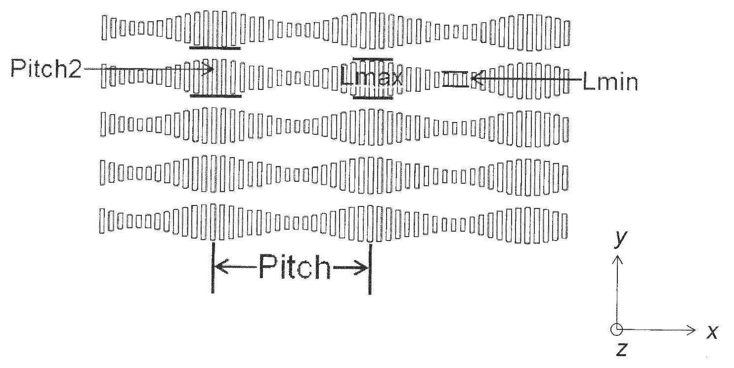
도 6은 그러한 타겟 구조의 예를 도시한다. 제 1 방향은 x 방향으로 도시되고 제 2 방향은 y 방향으로 도시된다. x 방향의 주기는 "Pitch"로 표시되고 y 방향의 주기는 "Pitch2"로 표시된다. 상기 제 1 방향의 주기는 상기 제 1 방향과 다른 방향의 상기 하나 이상의 패턴의 치수의 주기일 수 있다. 도 6의 예에서, 하나 이상의 패턴은 y 방향으로 연장되는 일련의 라인을 포함하고, 제 1 방향의 주기는 이들 라인의 길이에서의 주기이다. 라인들은 x 방향으로 동일한 폭을 가질 수 있다. 임의의 하나의 라인의 x 방향의 폭은 그 하나의 라인의 전체 길이를 따라 균일할 수 있다. 제 1 방향 이외의 다른 방향으로의 하나 이상의 패턴의 치수는 제 1 방향으로의 하나 이상의 패턴의 위치의 사인 함수일 수 있다.Figure 6 shows an example of such a target structure. The first direction is shown in the x direction and the second direction is shown in the y direction. The period in the x direction is indicated by "Pitch" and the period in the y direction is indicated by "Pitch2". The period in the first direction may be a period of a dimension of the at least one pattern in a direction different from the first direction. In the example of FIG. 6, the one or more patterns comprise a series of lines extending in the y direction, and the period in the first direction is a period in the length of these lines. The lines may have the same width in the x direction. The width of any one line in the x direction can be uniform along the entire length of that one line. The dimension of the one or more patterns in a direction other than the first direction may be a sine function of the position of the one or more patterns in the first direction.
이 예에서, y 방향의 라인의 길이는 최대 Lmax 및 최소 Lmin으로 변조된다. 인접한 Lmax와 Lmin의 위치들 사이의 간격은 Pitch의 절반일 수 있다. Lmax와 Lmin의 차이는 Pitch2보다 작거나 같을 수 있다. 도 10의 예와 같이 Lmax는 Pitch2만큼 클 수 있고 Lmin은 0만큼 작을 수 있다. 타겟 구조의 이러한 기하학적 파라미터들(예를 들어, Pitch, Pitch2, Lmax 및 Lmin)은 타겟 구조의 검출 가능성 및 인쇄 가능성을 향상시키도록 조정될 수 있다.In this example, the length of the line in the y direction is modulated to a maximum L max and a minimum L min . The spacing between adjacent L max and L min positions can be half of the pitch. The difference between L max and L min can be less than or equal to Pitch2. L max may be as large as Pitch2 L min, such as the example of FIG. 10 may be as small as zero. These geometric parameters of the target structure (e.g., Pitch, Pitch2, L max and L min) can be adjusted to improve the likelihood of detection and possible printing of the target structure.
하나 이상의 패턴이 지지되는 기판은 또한 전자 디바이스의 구조를 나타내는 패턴을 포함할 수 있다.The substrate on which the one or more patterns are supported may also include a pattern representing the structure of the electronic device.
본 명세서에 개시된 타겟 구조는 기판 상의 전자 디바이스를 제조하는데 사용되는 리소그래피 장치에서 기판을 정렬하는데 사용되는 정렬 타겟으로서 사용될 수 있다. 제 1 방향은 정렬 방향일 수 있다. 타겟 구조는 기판 상에 제조된 전자 디바이스의 단일 층에 대응하는 단일 층을 포함할 수 있다. 타겟 구조는 기판 상에 제조된 전자 디바이스의 2 개의 층에 대응하는 2 개의 층을 포함할 수 있다.The target structure disclosed herein can be used as an alignment target used to align a substrate in a lithographic apparatus used to manufacture an electronic device on a substrate. The first direction may be the alignment direction. The target structure may comprise a single layer corresponding to a single layer of the electronic device fabricated on the substrate. The target structure may comprise two layers corresponding to the two layers of the electronic device fabricated on the substrate.
일 실시 예에서, 타겟 구조는 전자 디바이스의 구조를 나타내는 패턴의 수차 감도에 근접한 매칭을 허용한다. 수차는 빔이 투영 광학계 및 다른 빔 형성 광학 요소를 통해 이동하는 경우의 파면 형상의 변화로 인해 발생한다. 메트롤로지 툴 및 리소그래피 장치는 동일한 광학 특성을 갖지 않을 수 있다. 타겟 구조는 메트롤로지 툴과 리소그래피 장치 사이의 수차 불일치에 대한 감도를 감소시키도록 구성될 수 있다. 타겟 구조는 (도 6의 경우와 같이) 하나의 마스크 또는 (도 7-9의 실시 예에 도시된 바와 같이) 2 개의 마스크를 사용하여 정의될 수 있다.In one embodiment, the target structure allows matching proximate to the aberration sensitivity of the pattern representing the structure of the electronic device. Aberrations occur due to changes in the wavefront shape when the beam travels through the projection optics and other beam forming optical elements. The metrology tool and the lithographic apparatus may not have the same optical properties. The target structure may be configured to reduce sensitivity to aberration mismatch between the metrology tool and the lithographic apparatus. The target structure may be defined using either one mask (as in the case of FIG. 6) or two masks (as shown in the embodiment of FIGS. 7-9).
도 6에 도시된 타겟 구조는 단일 마스크를 사용하여 제조될 수 있다. 도 7 및 도 8은 2 개의 마스크를 사용하여 도 6의 타겟 구조가 만들어질 수 있음을 나타낸다. 첫 번째 마스크는 도 7과 같이 밀도가 높은 균일한 라인을 포함한다. 제 1 마스크에서의 라인 및 공간 특성은 전자 디바이스의 구조를 나타내는 패턴과 거의 일치할 수 있다. 예를 들어, 라인들이 전자 디바이스의 구조를 나타내는 패턴들에 대해 소정 각도를 이루는 경우, 회전 다이폴 조명이 더 나은 메트롤로지 측정을 달성하기 위해 사용될 수 있다.The target structure shown in Figure 6 may be fabricated using a single mask. Figures 7 and 8 show that the target structure of Figure 6 can be made using two masks. The first mask includes a dense uniform line as shown in FIG. The line and space characteristics in the first mask may substantially coincide with the pattern representing the structure of the electronic device. For example, if the lines are at an angle to the patterns representing the structure of the electronic device, the rotating dipole illumination can be used to achieve better metrology measurements.
"컷 마스크(cut mask)"라고 하는 제 2 마스크가 도 8에 도시된다. 도 7의 제 1 마스크를 사용하여 만들어진 라인을 갖는 기판이 컷 마스크에 정렬되어 노광될 때, 라인의 일부가 제거된다. 라인의 나머지는 도 9a에 도시된 바와 같이 어두운 라인의 흰색 부분이다. 도 9b는 컷 마스크가 연속적인 계단식 구조(stair-case like structure)인 예를 도시한다. 계단의 가장자리는 두 개의 이웃한 라인들 사이에 위치할 수 있다.A second mask called "cut mask" is shown in FIG. When a substrate having lines made using the first mask of FIG. 7 is exposed in alignment with the cut mask, a portion of the line is removed. The rest of the line is the white portion of the dark line, as shown in FIG. 9A. Figure 9B shows an example where the cut mask is a stair-case like structure. The edge of the stair can be located between two neighboring lines.
본 명세서에 개시된 타겟 구조를 제조하는 방법은, 기판 상에 복수의 평행한 라인을 제조하는 단계; 상기 라인들의 길이를 변경함으로써 상기 하나 이상의 패턴들을 형성하는 단계를 포함한다. 상기 라인을 제조하는 단계는 제 1 패터닝 디바이스로 노광하는 단계를 포함할 수 있으며, 상기 패턴을 형성하는 단계는 제 2 패터닝 디바이스로 노광하는 단계를 포함할 수 있다.A method of manufacturing a target structure as disclosed herein includes the steps of: fabricating a plurality of parallel lines on a substrate; And forming the one or more patterns by varying the length of the lines. The step of fabricating the line may comprise exposing to the first patterning device, and the step of forming the pattern may comprise exposing the second patterning device.
기하학적 파라미터(예를 들어, Pitch, Pitch2, Lmax 및 Lmin)는 시뮬레이션에 의해 조정될 수 있다. 2 개의 마스크를 사용하는 예에서 기하학적 파라미터는 검출 가능성과 인쇄 가능성을 향상시키기 위해 조정될 수 있으며, 수차 매칭은 설계에 의해 달성될 수 있다. 하나의 마스크를 사용하는 예에서, 기하학적 파라미터는 양호한 검출성 및 인쇄 가능성뿐만 아니라 상대적으로 우수한 수차 매칭을 달성하도록 조정될 수 있다. 오버레이 타겟의 경우, 측정될 오버레이와 관련하여 다른 층의 타겟 파라미터와 결합하여 기하학적 파라미터 튜닝을 수행할 수 있다. 그러한 결합된 튜닝은 전형적으로 오버레이 타겟에 대한 더 우수한 수차 매칭 및 검출 가능성을 제공할 수 있다. 동일한 디바이스 층에서 정렬 타겟을 위해, 튜닝이 더 간단하다.Geometrical parameters (e. G., Pitch, Pitch2, L max and L min) can be adjusted by the simulation. In the example using two masks, geometric parameters can be adjusted to improve detectability and printability, and aberration matching can be achieved by design. In the example using one mask, the geometric parameters can be adjusted to achieve good aberration matching as well as good detectability and printability. In the case of an overlay target, geometric parameter tuning may be performed in conjunction with target parameters of other layers in relation to the overlay to be measured. Such combined tuning can typically provide better aberration matching and detectability for the overlay target. For an alignment target in the same device layer, tuning is simpler.
전술한 바와 같이, 도 6에 표시된 파라미터는 최적의 메트롤로지 성능을 달성하도록 튜닝되어 조정될 수 있다. 정현파 변조의 정도는 다를 수 있다. 도 10은 전체 변조를 사용하는 타겟의 예를 보여준다. 도 10에서 Pitch2 = Lmax이므로 중심 라인들이 연결되고 Lmin = 0이 된다. 파라미터 조정은 더 나은 메트롤로지 성능을 달성하는데 도움이 될 뿐만 아니라 기존 타겟이 달성할 수 없는 일부 설계 제약 조건을 준수하는데 도움이 된다.As described above, the parameters shown in Fig. 6 can be tuned and adjusted to achieve optimum metrology performance. The degree of sinusoidal modulation may be different. Figure 10 shows an example of a target using full modulation. Since in Fig. 10 Pitch2 = L max are the center line is connected and the L min = 0. Parameter tuning not only helps to achieve better metrology performance, but also helps to comply with some design constraints that existing targets can not achieve.
도 6-10의 상기 설명 및 도해는 x 방향으로 극 다이폴 조명(extreme dipole illumination)을 위한 것이다. y 방향의 극 다이폴 조명의 경우, 타겟은 일반적으로 90도 회전할 필요가 있다. 회전된 극 다이폴 조명의 경우 변조된 구조는 일반적으로 다이폴 조명 각도와 매칭하도록 회전하고 두 개의 마스크를 사용하여 생성될 때의 제품 피처와 일치한다. 이는 제품에 대한 우수한 수차 민감도 매칭과 향상된 인쇄성을 제공한다. 메트롤로지 구조가 단지 하나의 마스크를 사용하여 생성될 때, 설계자는 인쇄 가능성이 향상되면 다이폴 조명 각도와 일치하도록 격자 라인을 회전하도록 선택할 수 있다.The above description and illustration of Figures 6-10 is for extreme dipole illumination in the x direction. For a dipole illumination in the y direction, the target generally needs to be rotated 90 degrees. For rotated polar dipole illumination, the modulated structure is generally rotated to match the dipole illumination angle and coincides with the product feature as it is created using the two masks. This provides excellent aberration sensitivity matching and improved printability for the product. When the metrology structure is created using only one mask, the designer can choose to rotate the grid lines to match the dipole illumination angle as the printability improves.
도 11은 약간 수정된 실시 예를 도시한다. 도 6 내지 도 10에 도시된 실시 예들과 유사하게, 도 11의 실시 예는 또한 오버레이 및 정렬 측정을 위한 1 차 회절을 향상시키기 위해 측 방향 폭의 정현파 변조를 사용한다. 그러나, 전술한 실시 예에서와 같이 정현파 기하학적 형상을 구성하기 위해 작은 라인 세그먼트를 사용하는 대신에, 도 11의 실시 예는 주기적인 솔리드 사인 기하학적 형상을 타겟으로 직접 사용한다.Figure 11 shows a slightly modified embodiment. Similar to the embodiments shown in Figs. 6-10, the embodiment of Fig. 11 also uses lateral width sinusoidal modulation to improve first order diffraction for overlay and alignment measurements. However, instead of using a small line segment to construct a sinusoidal geometry, as in the previous embodiments, the embodiment of Figure 11 directly uses a periodic solid sine geometry shape as a target.
본 개시는 오버레이 및 정렬 측정을 위해 변조된 횡 방향 폭을 갖는 타겟을 사용할 수 있다. 타겟 설계 동안, 다양한 기하학적 파라미터(예를 들어, 피치 및 격자 라인의 상이한 횡 방향 폭)가 양호한 검출 가능성, 인쇄성 및 수차 매칭을 달성하도록 최적화될 수 있다. 도 12는 본 개시에 따라 변조된 기하학적 파라미터를 사용하여 메트롤로지 타겟을 설계하는 방법의 흐름도(1200)를 도시한다.The present disclosure may use a target having a modulated lateral width for overlay and alignment measurements. During the target design, various geometric parameters (e.g., different transverse widths of pitch and lattice lines) can be optimized to achieve good detectability, printability and aberration matching. Figure 12 shows a flow diagram 1200 of a method for designing a metrology target using geometric parameters modulated in accordance with the present disclosure.
블록(1202)은 리소그래피 프로세스 흐름 파라미터(1204), 메트롤로지 툴 세팅 및 타겟 기하학적 파라미터(1206), 및 사용될 리소그래피 모델(1208) 예를 들어 포커스 노광 모델을 포함하는, 타겟 설계용 다양한 입력을 나타낸다. 곡선(curvilinear) 기하학적 구조 파라미터는 블록(1206)에서 입력될 수 있다.
블록(1210)은 공칭 조건에서 메트롤로지 툴 검출성 키 성능 지수(KPI)를 시뮬레이션한다. 블록(1214)은 공칭 조건에서 리소그래피 인쇄성 KPI를 시뮬레이션한다.
당업자는 추가의 단계들이 프로세스 흐름에 추가될 수 있고 및/또는 흐름도에 도시된 일부 단계들은 본 개시의 범위를 벗어나지 않고 특정 리소그래피 프로세스에 특정한 단계들로 대체될 수 있음을 이해할 것이다. 블록(1212)은 불량 검출성 및 인쇄성을 가진 타깃을 걸러 낸다. 블록(1216)은 측정 견실도의 시뮬레이션을 나타낸다. 구체적으로, 블록(1218)은 검출성 견실도 KPI를 시뮬레이션하고, 블록(1220)은 오버레이 견실도 KPI를 시뮬레이션하며, 블록(1222)은 수차 민감도 KPI를 시뮬레이션한다.Those skilled in the art will appreciate that additional steps may be added to the process flow and / or some of the steps shown in the flowchart may be replaced by steps specific to a particular lithographic process without departing from the scope of the present disclosure.
마지막으로, 블록(1224)에서, 적절한 KPI(또는 가중 KPI)를 갖는 메트롤로지 타겟이 실제 측정을 위해 선택된다.Finally, at
2 개의 층 각각은 타겟 구조를 포함하고, 층들 중 적어도 하나 상의 타겟 구조는 여기에 개시된 타겟 구조이며, 이들은 전자 디바이스의 층 간의 오버레이를 측정하는데 사용될 수 있다. 오버레이를 측정하는 방법은 타겟 구조로부터 회절 차수를 측정하는 단계; 회절 차수들로부터 오버레이 오차를 결정하는 단계를 포함한다.Each of the two layers includes a target structure, and the target structure on at least one of the layers is the target structure disclosed herein, which can be used to measure the overlay between layers of the electronic device. A method of measuring an overlay includes measuring a diffraction order from a target structure; And determining an overlay error from the diffraction orders.
본 명세서에 개시된 타겟 구조는 기판이 타겟 구조를 그 위에 포함할 때 기판 상의 기존 구조에 정렬하기 위해 사용될 수 있다. 정렬 방법은 상기 타겟 구조로부터 회절 차수를 측정하고 상기 회절 차수들로부터 정렬 오차를 결정하는 단계를 포함한다.The target structures disclosed herein can be used to align existing structures on a substrate when the substrate includes a target structure thereon. The alignment method includes measuring a diffraction order from the target structure and determining an alignment error from the diffraction orders.
타겟 구조는 컴퓨터 판독 가능 비-일시적인 매체 상에 저장된 전자 데이터에 의해 표현될 수 있다.The target structure may be represented by electronic data stored on a computer-readable non-transitory medium.
일 실시 예에 의하면, 기판 상의 타겟 구조를 사용하여 정렬 또는 오버레이를 측정하는 방법으로서, 상기 타겟 구조로부터 제 1 방향으로의 회절 차수를 측정하는 단계 - 상기 타겟 구조는 상기 제 1 차수보다 높은 회절 차수를 희생시키면서 상기 제 1 방향으로의 회절의 제 1 차수를 향상시키도록 구성되며, 상기 타겟 구조로부터 제 2 방향으로의 회절은 0 차 차수만을 가지며, 상기 제 1 방향 및 상기 제 2 방향은 상이하고 상기 기판에 평행함 -; 및 상기 제 1 방향의 회절 차수로부터 정렬 오차 또는 오버레이 오차를 결정하는 단계를 포함한다. 상기 제 1 차수보다 큰 상기 제 1 방향의 회절 차수는 상기 타겟 구조에 의해 향상되지 않는다.According to one embodiment, there is provided a method of measuring alignment or overlay using a target structure on a substrate, the method comprising measuring a diffraction order in a first direction from the target structure, the target structure having a diffraction order Wherein diffraction from the target structure in a second direction has only a zeroth order, wherein the first direction and the second direction are different Parallel to the substrate; And determining an alignment error or an overlay error from the diffraction order in the first direction. The diffraction order in the first direction greater than the first order is not improved by the target structure.
본 발명은 다음의 항목을 사용하여 더 설명될 수 있다:The invention may be further illustrated by means of the following items:
1. 타겟 구조로서,1. As a target structure,
상기 타겟 구조는 메트롤로지 툴로 측정되도록 구성되며, 상기 메트롤로지 툴은 회절 임계치를 갖고;Wherein the target structure is configured to be measured with a metrology tool, the metrology tool having a diffraction threshold;
상기 타겟 구조는:The target structure comprises:
기판 상에 지지된 하나 이상의 패턴들을 포함하고,Comprising at least one pattern supported on a substrate,
상기 하나 이상의 패턴은 제 1 방향으로 제 1 주기로 주기적이고 제 2 방향으로 제 2 주기로 주기적이며, 상기 제 1 방향 및 제 2 방향은 상이하고 상기 기판에 평행하며,Wherein the at least one pattern is periodic at a first period in a first direction and at a second period in a second direction, the first direction and the second direction being different and parallel to the substrate,
상기 제 1 주기는 상기 회절 임계치와 동일하거나 그보다 크며, 상기 제 2주기는 상기 회절 임계치보다 작으며,Wherein the first period is equal to or greater than the diffraction threshold, the second period is less than the diffraction threshold,
상기 하나 이상의 패턴은 상기 제 1 차수보다 높은 회절 차수를 희생하면서 상기 제 1 방향으로 상기 타겟 구조로부터의 제 1 차 회절을 향상시키도록 구성되는 타겟 구조.Wherein the at least one pattern is configured to enhance a first order diffraction from the target structure in the first direction at a sacrifice of a diffraction order higher than the first order.
2. 제 1 항에 있어서, 상기 하나 이상의 패턴은 상기 제 2 방향에서의 상기 타겟 구조로부터의 회절이 단지 0 차(zero-th)를 갖도록 구성되는 타겟 구조.2. The target structure of
3. 제 1 항 내지 제 2 항 중 어느 한 항에 있어서, 상기 하나 이상의 패턴은 메트롤로지 툴이 하나 이상의 패턴으로부터 정렬 또는 오버레이를 측정할 수 있도록 구성되는 타겟 구조.3. The target structure of any one of
4. 제 1 항 내지 제 3 항 중 어느 한 항에 있어서, 상기 하나 이상의 패턴은 포토 레지스트로 형성되는 타겟 구조.4. The target structure according to any one of
5. 제 1 항 내지 제 4 항 중 어느 한 항에 있어서, 상기 하나 이상의 패턴은 상기 기판 내로 에칭되는 타겟 구조.5. The target structure according to any one of
6. 제 1 항 내지 제 5 항 중 어느 한 항에 있어서, 상기 하나 이상의 패턴은 상기 패턴을 둘러싸는 객체와는 상기 기판에 수직한 방향으로 상이한 높이를 갖는 타겟 구조.6. The target structure of any one of
7. 제 1 항 내지 제 6 항 중 어느 한 항에 있어서, 상기 하나 이상의 패턴은 상기 패턴을 둘러싸는 객체와는 상이한 광학 특성을 갖는 타겟 구조.7. The target structure according to any one of
8. 제 1 항 내지 제 7 항 중 어느 한 항에 있어서, 상기 제 1 방향은 상기 제 2 방향에 수직인 타겟 구조.8. The target structure according to any one of
9. 제 1 항 내지 제 8 항 중 어느 한 항에 있어서, 상기 제 1 주기는 상기 제 1 방향 이외의 방향으로 상기 하나 이상의 패턴의 치수의 주기인 타겟 구조.9. The target structure according to any one of
10. 제 1 항 내지 제 9 항 중 어느 한 항에 있어서, 상기 제 1 방향 이외의 방향으로 상기 하나 이상의 패턴의 치수는 상기 제 1 방향으로 상기 하나 이상의 패턴의 위치의 사인 함수인 타겟 구조.10. The target structure according to any one of
11. 제 1 항 내지 제 10 항 중 어느 한 항에 있어서, 상기 하나 이상의 패턴은 상기 제 2 방향의 라인을 포함하는 타겟 구조.11. The target structure according to any one of
12. 제 11 항에 있어서, 상기 라인은 상기 제 1 방향으로 동일한 크기를 갖는 타겟 구조.12. The target structure of
13. 제 11 항에 있어서, 상기 라인 각각은 상기 제 1 방향으로 균일한 크기를 갖는 타겟 구조.13. The target structure of
14. 기판으로서, 제 1 항 내지 제 13 항 중 어느 한 항의 타겟 구조와 전자 디바이스의 구조를 나타내는 패턴을 포함하는 기판.14. A substrate comprising a target structure according to any one of
15. 제 1 항 내지 제 13 항 중 어느 한 항에 따른 타겟 구조를 제조하는 방법으로서,15. A method of manufacturing a target structure according to any one of
상기 기판 상에 복수의 평행한 라인을 제조하는 단계;Fabricating a plurality of parallel lines on the substrate;
상기 라인의 길이를 변경함으로써 상기 하나 이상의 패턴들을 형성하는 단계를 포함하는 방법.And forming the one or more patterns by varying the length of the line.
16. 제 15 항에 있어서, 상기 라인을 제조하는 단계는 제 1 패터닝 디바이스로 노광하는 단계를 포함하고, 상기 패턴을 형성하는 단계는 제 2 패터닝 디바이스로 노광하는 단계를 포함하는 방법.16. The method of claim 15, wherein the step of fabricating the line comprises exposing to a first patterning device, and wherein forming the pattern comprises exposing to a second patterning device.
17. 전자 디바이스의 2 개의 상이한 층 상의 구조 사이의 오버레이를 측정하는 컴퓨터 구현 방법으로서, 상기 2 개의 층 각각은 타겟 구조를 포함하고, 상기 2 개의 층 상의 타겟 구조 중 하나 이상은 제 1 항 내지 제 13 항 중 어느 한 항의 타겟 구조이며, 상기 방법은:17. A computer-implemented method for measuring an overlay between structures on two different layers of an electronic device, each of the two layers comprising a target structure, wherein at least one of the target structures on the two layers comprises a first 13. A target structure according to any one of
상기 타겟 구조로부터 회절 차수를 측정하는 단계;Measuring a diffraction order from the target structure;
상기 회절 차수로부터 오버레이 오차를 결정하는 단계를 포함하는 방법.And determining an overlay error from the diffraction order.
18. 기판 상에 존재하는 구조에 정렬시키는 컴퓨터 구현 방법으로서, 상기 기판은 제 1 항 내지 제 13 항 중 어느 한 항의 타겟 구조를 포함하며, 상기 방법은:18. A computer-implemented method for aligning to a structure present on a substrate, the substrate comprising the target structure of any one of
상기 타겟 구조로부터 회절 차수를 측정하는 단계;Measuring a diffraction order from the target structure;
상기 회절 차수로부터 정렬 오차를 결정하는 단계를 포함하는 방법.And determining an alignment error from the diffraction order.
19. 전자 데이터가 저장된 컴퓨터 판독 가능 비-일시적인 매체로서, 상기 전자 데이터는 제 1 항 내지 제 13 항 중 어느 한 항의 타겟 구조를 표현하는 매체.19. A computer readable non-transitory medium in which electronic data is stored, the electronic data representing the target structure of any one of
20. 기판 상의 타겟 구조를 사용하여 정렬 또는 오버레이를 측정하는 방법으로서,20. A method of measuring alignment or overlay using a target structure on a substrate,
상기 타겟 구조로부터 제 1 방향으로의 회절 차수를 측정하는 단계 - 상기 타겟 구조는 상기 제 1 차수보다 높은 회절 차수를 희생시키면서 상기 제 1 방향으로의 회절의 제 1 차수를 향상시키도록 구성되며, 상기 타겟 구조로부터 제 2 방향으로의 회절은 0 차 차수만을 가지며, 상기 제 1 방향 및 상기 제 2 방향은 상이하고 상기 기판에 평행함 -; 및Measuring a diffraction order in a first direction from the target structure, the target structure being configured to enhance a first order of diffraction in the first direction at the expense of a diffraction order higher than the first order, Wherein the diffraction from the target structure in the second direction has only a zero order degree, the first direction and the second direction being different and parallel to the substrate; And
상기 제 1 방향의 회절 차수로부터 정렬 오차 또는 오버레이 오차를 결정하는 단계Determining an alignment error or an overlay error from the diffraction order in the first direction
를 포함하는 방법.≪ / RTI >
21. 제 20 항에 있어서, 상기 제 1 차수보다 큰 상기 제 1 방향의 회절 차수는 상기 타겟 구조에 의해 향상되지 않는 방법.21. The method of
22. 제 20 항 내지 제 21 항 중 어느 한 항에 있어서, 상기 제 1 방향은 상기 제 2 방향에 수직인 방법.22. The method according to any one of
23. 제 20 항 내지 제 21 항 중 어느 한 항에 있어서, 상기 타겟 구조는 하나 이상의 패턴을 포함하고, 상기 하나 이상의 패턴은 상기 제 1 방향으로의 제 1 주기로 주기적이고 상기 제 2 방향으로의 제 2 주기로 주기적인 방법.23. The method of any one of
24. 제 23 항에 있어서, 상기 제 1 주기는 상기 제 1 방향을 제외한 방향으로의 하나 이상의 패턴들의 치수의 주기인 방법.24. The method of
25. 제 20 항 내지 제 24 항 중 어느 한 항에 있어서, 상기 타겟 구조는 포토 레지스트로 형성되는 방법.25. The method of any one of
26. 제 20 항 내지 제 24 항 중 어느 한 항에 있어서, 상기 타겟 구조는 상기 기판 내로 에칭되는 방법.26. The method of any one of
27. 제 20 항 내지 제 26 항 중 어느 한 항에 있어서, 상기 타겟 구조는 상기 제 2 방향의 라인을 포함하는 방법.27. The method of any of
28. 제 27 항에 있어서, 상기 라인은 상기 제 1 방향으로 동일한 크기를 갖는 방법.28. The method of claim 27, wherein the lines have the same size in the first direction.
29. 제 27 항에 있어서, 상기 라인 각각은 상기 제 1 방향으로 균일한 크기를 갖는 방법.29. The method of claim 27, wherein each of the lines has a uniform size in the first direction.
30. 명령들을 갖는 컴퓨터 판독 가능 비-일시적인 매체로서, 상기 명령들은, 컴퓨터에 의해 실행될 때, 제 20 항 내지 제 29 항 중 어느 한 항의 방법을 구현하는 매체.30. A computer-readable non-transitory medium having instructions, when executed by a computer, to implement the method of any of
위의 설명은 설명을 위한 것이지 제한적인 것은 아니다. 따라서, 이하에 설명된 청구범위의 범주를 벗어나지 않고 기술된 실시 예에 대한 수정이 이루어질 수 있음은 당업자에게 명백할 것이다.The above description is intended to be illustrative, not limiting. Thus, it will be apparent to those skilled in the art that modifications may be made to the embodiments described without departing from the scope of the claims set forth below.
Claims (15)
상기 타겟 구조는 메트롤로지 툴로 측정되도록 구성되며, 상기 메트롤로지 툴은 회절 임계치를 갖고;
상기 타겟 구조는:
기판 상에 지지된 하나 이상의 패턴들을 포함하고,
상기 하나 이상의 패턴은 제 1 방향으로 제 1 주기로 주기적이고 제 2 방향으로 제 2 주기로 주기적이며, 상기 제 1 방향 및 제 2 방향은 상이하고 상기 기판에 평행하며,
상기 제 1 주기는 상기 회절 임계치와 동일하거나 그보다 크며, 상기 제 2주기는 상기 회절 임계치보다 작으며,
상기 하나 이상의 패턴은 상기 제 1 차수보다 높은 회절 차수를 희생하면서 상기 제 1 방향으로 상기 타겟 구조로부터의 제 1 차 회절을 향상시키도록 구성되는 타겟 구조.As a target structure,
Wherein the target structure is configured to be measured with a metrology tool, the metrology tool having a diffraction threshold;
The target structure comprises:
Comprising at least one pattern supported on a substrate,
Wherein the at least one pattern is periodic at a first period in a first direction and at a second period in a second direction, the first direction and the second direction being different and parallel to the substrate,
Wherein the first period is equal to or greater than the diffraction threshold, the second period is less than the diffraction threshold,
Wherein the at least one pattern is configured to enhance a first order diffraction from the target structure in the first direction at a sacrifice of a diffraction order higher than the first order.
상기 타겟 구조로부터 회절 차수를 측정하는 단계;
상기 회절 차수로부터 오버레이 오차를 결정하는 단계를 포함하는 방법.A computer-implemented method of measuring an overlay between structures on two different layers of an electronic device, wherein each of the two layers comprises a target structure, and at least one of the target structures on the two layers is the target structure of claim 1, The method comprising:
Measuring a diffraction order from the target structure;
And determining an overlay error from the diffraction order.
상기 타겟 구조로부터 회절 차수를 측정하는 단계;
상기 회절 차수로부터 정렬 오차를 결정하는 단계를 포함하는 방법.A computer-implemented method for aligning to a structure present on a substrate, the substrate comprising the target structure of claim 1, the method comprising:
Measuring a diffraction order from the target structure;
And determining an alignment error from the diffraction order.
상기 타겟 구조로부터 제 1 방향으로의 회절 차수를 측정하는 단계 - 상기 타겟 구조는 상기 제 1 차수보다 높은 회절 차수를 희생시키면서 상기 제 1 방향으로의 회절의 제 1 차수를 향상시키도록 구성되며, 상기 타겟 구조로부터 제 2 방향으로의 회절은 0 차 차수만을 가지며, 상기 제 1 방향 및 상기 제 2 방향은 상이하고 상기 기판에 평행함 -; 및
상기 제 1 방향의 회절 차수로부터 정렬 오차 또는 오버레이 오차를 결정하는 단계
를 포함하는 방법.A method of measuring alignment or overlay using a target structure on a substrate,
Measuring a diffraction order in a first direction from the target structure, the target structure being configured to enhance a first order of diffraction in the first direction at the expense of a diffraction order higher than the first order, Wherein the diffraction from the target structure in the second direction has only a zero order degree, the first direction and the second direction being different and parallel to the substrate; And
Determining an alignment error or an overlay error from the diffraction order in the first direction
≪ / RTI >
Applications Claiming Priority (3)
| Application Number | Priority Date | Filing Date | Title |
|---|---|---|---|
| US201562387571P | 2015-12-28 | 2015-12-28 | |
| US62/387,571 | 2015-12-28 | ||
| PCT/EP2016/080742 WO2017114652A1 (en) | 2015-12-28 | 2016-12-13 | Alternative target design for metrology using modulation techniques |
Publications (2)
| Publication Number | Publication Date |
|---|---|
| KR20180098378A true KR20180098378A (en) | 2018-09-03 |
| KR102170147B1 KR102170147B1 (en) | 2020-10-27 |
Family
ID=57543043
Family Applications (1)
| Application Number | Title | Priority Date | Filing Date |
|---|---|---|---|
| KR1020187021658A Active KR102170147B1 (en) | 2015-12-28 | 2016-12-13 | Alternative target design for metrology using modulation technology |
Country Status (4)
| Country | Link |
|---|---|
| US (1) | US10585357B2 (en) |
| KR (1) | KR102170147B1 (en) |
| TW (1) | TWI623823B (en) |
| WO (1) | WO2017114652A1 (en) |
Cited By (1)
| Publication number | Priority date | Publication date | Assignee | Title |
|---|---|---|---|---|
| KR20220132634A (en) * | 2020-03-02 | 2022-09-30 | 에이에스엠엘 네델란즈 비.브이. | How to infer local uniformity metrics |
Families Citing this family (12)
| Publication number | Priority date | Publication date | Assignee | Title |
|---|---|---|---|---|
| WO2018156702A1 (en) * | 2017-02-23 | 2018-08-30 | Nikon Corporation | Measurement of a change in a geometrical characteristic and/or position of a workpiece |
| US10705435B2 (en) | 2018-01-12 | 2020-07-07 | Globalfoundries Inc. | Self-referencing and self-calibrating interference pattern overlay measurement |
| US10677588B2 (en) * | 2018-04-09 | 2020-06-09 | Kla-Tencor Corporation | Localized telecentricity and focus optimization for overlay metrology |
| US11055464B2 (en) | 2018-08-14 | 2021-07-06 | Taiwan Semiconductor Manufacturing Co., Ltd. | Critical dimension uniformity |
| NL2024878A (en) * | 2019-02-19 | 2020-08-27 | Asml Holding Nv | Metrology system, lithographic apparatus, and method |
| US11256177B2 (en) | 2019-09-11 | 2022-02-22 | Kla Corporation | Imaging overlay targets using Moiré elements and rotational symmetry arrangements |
| US11686576B2 (en) | 2020-06-04 | 2023-06-27 | Kla Corporation | Metrology target for one-dimensional measurement of periodic misregistration |
| US11796925B2 (en) | 2022-01-03 | 2023-10-24 | Kla Corporation | Scanning overlay metrology using overlay targets having multiple spatial frequencies |
| US12032300B2 (en) | 2022-02-14 | 2024-07-09 | Kla Corporation | Imaging overlay with mutually coherent oblique illumination |
| US12487190B2 (en) | 2022-03-30 | 2025-12-02 | Kla Corporation | System and method for isolation of specific fourier pupil frequency in overlay metrology |
| US12422363B2 (en) | 2022-03-30 | 2025-09-23 | Kla Corporation | Scanning scatterometry overlay metrology |
| US12235588B2 (en) | 2023-02-16 | 2025-02-25 | Kla Corporation | Scanning overlay metrology with high signal to noise ratio |
Citations (4)
| Publication number | Priority date | Publication date | Assignee | Title |
|---|---|---|---|---|
| US7671990B1 (en) * | 2006-07-28 | 2010-03-02 | Kla-Tencor Technologies Corporation | Cross hatched metrology marks and associated method of use |
| JP2011009259A (en) * | 2009-06-23 | 2011-01-13 | Renesas Electronics Corp | Semiconductor device, lithography method, and method of manufacturing semiconductor device |
| US20150293458A1 (en) * | 2012-11-30 | 2015-10-15 | Asml Netherlands B.V. | Method of Determining Dose and Focus, Inspection Apparatus, Patterning Device, Substrate and Device Manufacturing Method |
| KR20150130501A (en) * | 2013-03-14 | 2015-11-23 | 에이에스엠엘 네델란즈 비.브이. | Patterning device, method of producing a marker on a substrate and device manufacturing method |
Family Cites Families (6)
| Publication number | Priority date | Publication date | Assignee | Title |
|---|---|---|---|---|
| TW556296B (en) | 2000-12-27 | 2003-10-01 | Koninkl Philips Electronics Nv | Method of measuring alignment of a substrate with respect to a reference alignment mark |
| US7626701B2 (en) | 2004-12-27 | 2009-12-01 | Asml Netherlands B.V. | Lithographic apparatus with multiple alignment arrangements and alignment measuring method |
| TWI596444B (en) | 2006-08-31 | 2017-08-21 | 尼康股份有限公司 | Exposure method and device, and device manufacturing method |
| SG153747A1 (en) | 2007-12-13 | 2009-07-29 | Asml Netherlands Bv | Alignment method, alignment system and product with alignment mark |
| NL1036702A1 (en) | 2008-04-15 | 2009-10-19 | Asml Holding Nv | Diffraction elements for alignment targets. |
| NL2002954A1 (en) | 2008-06-11 | 2009-12-14 | Asml Netherlands Bv | Sub-segmented alignment mark arrangement. |
-
2016
- 2016-12-13 US US16/063,190 patent/US10585357B2/en active Active
- 2016-12-13 WO PCT/EP2016/080742 patent/WO2017114652A1/en not_active Ceased
- 2016-12-13 KR KR1020187021658A patent/KR102170147B1/en active Active
- 2016-12-27 TW TW105143319A patent/TWI623823B/en not_active IP Right Cessation
Patent Citations (4)
| Publication number | Priority date | Publication date | Assignee | Title |
|---|---|---|---|---|
| US7671990B1 (en) * | 2006-07-28 | 2010-03-02 | Kla-Tencor Technologies Corporation | Cross hatched metrology marks and associated method of use |
| JP2011009259A (en) * | 2009-06-23 | 2011-01-13 | Renesas Electronics Corp | Semiconductor device, lithography method, and method of manufacturing semiconductor device |
| US20150293458A1 (en) * | 2012-11-30 | 2015-10-15 | Asml Netherlands B.V. | Method of Determining Dose and Focus, Inspection Apparatus, Patterning Device, Substrate and Device Manufacturing Method |
| KR20150130501A (en) * | 2013-03-14 | 2015-11-23 | 에이에스엠엘 네델란즈 비.브이. | Patterning device, method of producing a marker on a substrate and device manufacturing method |
Cited By (1)
| Publication number | Priority date | Publication date | Assignee | Title |
|---|---|---|---|---|
| KR20220132634A (en) * | 2020-03-02 | 2022-09-30 | 에이에스엠엘 네델란즈 비.브이. | How to infer local uniformity metrics |
Also Published As
| Publication number | Publication date |
|---|---|
| US10585357B2 (en) | 2020-03-10 |
| WO2017114652A1 (en) | 2017-07-06 |
| TW201734657A (en) | 2017-10-01 |
| KR102170147B1 (en) | 2020-10-27 |
| TWI623823B (en) | 2018-05-11 |
| US20180373168A1 (en) | 2018-12-27 |
Similar Documents
| Publication | Publication Date | Title |
|---|---|---|
| KR101710014B1 (en) | Method of determining dose and focus, inspection apparatus, patterning device, substrate and device manufacturing method | |
| KR102170147B1 (en) | Alternative target design for metrology using modulation technology | |
| US9939735B2 (en) | Method of determining focus, inspection apparatus, patterning device, substrate and device manufacturing method | |
| US20200348605A1 (en) | Inspection Apparatus and Methods, Substrates Having Metrology Targets, Lithographic System and Device Manufacturing Method | |
| US9811003B2 (en) | Metrology method and apparatus, substrate, lithographic system and device manufacturing method | |
| US9069264B2 (en) | Metrology method and apparatus, and device manufacturing method | |
| NL2010988A (en) | Metrology method and apparatus, lithographic system, device manufacturing method and substrate. | |
| KR20180049220A (en) | Metrology method and apparatus, lithographic system and device manufacturing method | |
| CN111065974B (en) | Beat patterns for alignment on small measurement targets | |
| KR20140139080A (en) | Metrology method and apparatus, lithographic system and device manufacturing method | |
| CN108292108A (en) | Measure target, method and apparatus, computer program and lithography system | |
| US20160026096A1 (en) | Method of Determining Dose, Inspection Apparatus, Patterning Device, Substrate and Device Manufacturing Method | |
| KR20180095604A (en) | Adjustment of the metrology device or measurement based on the characteristics of the measurement target |
Legal Events
| Date | Code | Title | Description |
|---|---|---|---|
| A201 | Request for examination | ||
| PA0105 | International application |
Patent event date: 20180726 Patent event code: PA01051R01D Comment text: International Patent Application |
|
| PA0201 | Request for examination | ||
| PG1501 | Laying open of application | ||
| E902 | Notification of reason for refusal | ||
| PE0902 | Notice of grounds for rejection |
Comment text: Notification of reason for refusal Patent event date: 20200224 Patent event code: PE09021S01D |
|
| E701 | Decision to grant or registration of patent right | ||
| PE0701 | Decision of registration |
Patent event code: PE07011S01D Comment text: Decision to Grant Registration Patent event date: 20200724 |
|
| GRNT | Written decision to grant | ||
| PR0701 | Registration of establishment |
Comment text: Registration of Establishment Patent event date: 20201020 Patent event code: PR07011E01D |
|
| PR1002 | Payment of registration fee |
Payment date: 20201021 End annual number: 3 Start annual number: 1 |
|
| PG1601 | Publication of registration | ||
| PR1001 | Payment of annual fee |
Payment date: 20231010 Start annual number: 4 End annual number: 4 |
|
| PR1001 | Payment of annual fee |
Payment date: 20241008 Start annual number: 5 End annual number: 5 |