KR20180098140A - Dynamically adjustable antennas for wearable devices - Google Patents
Dynamically adjustable antennas for wearable devices Download PDFInfo
- Publication number
- KR20180098140A KR20180098140A KR1020180018472A KR20180018472A KR20180098140A KR 20180098140 A KR20180098140 A KR 20180098140A KR 1020180018472 A KR1020180018472 A KR 1020180018472A KR 20180018472 A KR20180018472 A KR 20180018472A KR 20180098140 A KR20180098140 A KR 20180098140A
- Authority
- KR
- South Korea
- Prior art keywords
- antenna
- circuitry
- rssi
- radio frequency
- electronic device
- Prior art date
- Legal status (The legal status is an assumption and is not a legal conclusion. Google has not performed a legal analysis and makes no representation as to the accuracy of the status listed.)
- Granted
Links
Images


Classifications
-
- H—ELECTRICITY
- H04—ELECTRIC COMMUNICATION TECHNIQUE
- H04B—TRANSMISSION
- H04B17/00—Monitoring; Testing
- H04B17/30—Monitoring; Testing of propagation channels
- H04B17/309—Measuring or estimating channel quality parameters
- H04B17/318—Received signal strength
-
- H—ELECTRICITY
- H01—ELECTRIC ELEMENTS
- H01Q—ANTENNAS, i.e. RADIO AERIALS
- H01Q1/00—Details of, or arrangements associated with, antennas
- H01Q1/36—Structural form of radiating elements, e.g. cone, spiral, umbrella; Particular materials used therewith
- H01Q1/38—Structural form of radiating elements, e.g. cone, spiral, umbrella; Particular materials used therewith formed by a conductive layer on an insulating support
-
- G—PHYSICS
- G04—HOROLOGY
- G04G—ELECTRONIC TIME-PIECES
- G04G17/00—Structural details; Housings
- G04G17/08—Housings
-
- G—PHYSICS
- G04—HOROLOGY
- G04G—ELECTRONIC TIME-PIECES
- G04G9/00—Visual time or date indication means
- G04G9/08—Visual time or date indication means by building-up characters using a combination of indicating elements, e.g. by using multiplexing techniques
- G04G9/12—Visual time or date indication means by building-up characters using a combination of indicating elements, e.g. by using multiplexing techniques using light valves, e.g. liquid crystals
-
- H—ELECTRICITY
- H01—ELECTRIC ELEMENTS
- H01Q—ANTENNAS, i.e. RADIO AERIALS
- H01Q1/00—Details of, or arrangements associated with, antennas
- H01Q1/27—Adaptation for use in or on movable bodies
- H01Q1/273—Adaptation for carrying or wearing by persons or animals
-
- H—ELECTRICITY
- H01—ELECTRIC ELEMENTS
- H01Q—ANTENNAS, i.e. RADIO AERIALS
- H01Q1/00—Details of, or arrangements associated with, antennas
- H01Q1/50—Structural association of antennas with earthing switches, lead-in devices or lightning protectors
-
- H—ELECTRICITY
- H01—ELECTRIC ELEMENTS
- H01Q—ANTENNAS, i.e. RADIO AERIALS
- H01Q13/00—Waveguide horns or mouths; Slot antennas; Leaky-waveguide antennas; Equivalent structures causing radiation along the transmission path of a guided wave
- H01Q13/02—Waveguide horns
-
- H—ELECTRICITY
- H01—ELECTRIC ELEMENTS
- H01Q—ANTENNAS, i.e. RADIO AERIALS
- H01Q23/00—Antennas with active circuits or circuit elements integrated within them or attached to them
-
- H—ELECTRICITY
- H04—ELECTRIC COMMUNICATION TECHNIQUE
- H04B—TRANSMISSION
- H04B1/00—Details of transmission systems, not covered by a single one of groups H04B3/00 - H04B13/00; Details of transmission systems not characterised by the medium used for transmission
- H04B1/38—Transceivers, i.e. devices in which transmitter and receiver form a structural unit and in which at least one part is used for functions of transmitting and receiving
- H04B1/3827—Portable transceivers
- H04B1/385—Transceivers carried on the body, e.g. in helmets
Landscapes
- Engineering & Computer Science (AREA)
- Physics & Mathematics (AREA)
- Computer Networks & Wireless Communication (AREA)
- Signal Processing (AREA)
- Quality & Reliability (AREA)
- Electromagnetism (AREA)
- General Physics & Mathematics (AREA)
- Chemical & Material Sciences (AREA)
- Crystallography & Structural Chemistry (AREA)
- Support Of Aerials (AREA)
- Details Of Aerials (AREA)
- Telephone Function (AREA)
- Telephone Set Structure (AREA)
Abstract
손목시계와 같은 전자 디바이스는 유전체 후방 벽을 갖는 하우징을 포함할 수 있다. 디바이스 내의 무선 회로부는 후방 벽 상에 또는 그 위에 형성된 안테나를 포함할 수 있다. 매칭 회로부는 안테나의 임피던스를 무선 회로부의 나머지 부분에 매칭시킬 수 있다. 처리 회로부는 후방 벽을 통해 수신된 무선 주파수 신호들로부터 수신 신호 강도 정보 및/또는 위상 및 크기 정보를 수집할 수 있다. 처리 회로부는 디바이스의 위치를 추적하고 시간 경과에 따라 사용자 통계치들을 축적할 수 있다. 처리 회로부는 수신 신호 강도 정보, 사용자 통계치들, 및/또는 위상 및 크기 정보에 기초하여 유전체 후방 하우징 벽을 통한 안테나의 로딩(loading)의 변화가 발생했는지 여부를 결정할 수 있다. 변화가 검출되는 경우, 처리 회로부는 변화의 결과로서의 임의의 잠재적 안테나 디튜닝을 완화시키기 위해 매칭 회로부를 조정할 수 있다. An electronic device such as a wristwatch may include a housing having a dielectric back wall. The wireless circuitry in the device may comprise an antenna formed on or on the back wall. The matching circuitry may match the impedance of the antenna to the rest of the wireless circuitry. The processing circuitry may collect received signal strength information and / or phase and magnitude information from the radio frequency signals received via the back wall. The processing circuitry can track the location of the device and accumulate user statistics over time. The processing circuitry may determine whether a change in loading of the antenna through the dielectric rear housing wall has occurred, based on received signal strength information, user statistics, and / or phase and magnitude information. When a change is detected, the processing circuitry may adjust the matching circuitry to mitigate any potential antenna detuning as a result of the change.
Description
본 출원은 2017년 2월 24일자로 출원된 미국 특허 출원 제15/442,463호에 대한 우선권을 주장하며, 그 전문이 본 명세서에 참조로서 편입된다.This application claims priority to U.S. Patent Application No. 15 / 442,463, filed February 24, 2017, the entirety of which is incorporated herein by reference.
본 출원은 전자 디바이스에 관한 것으로, 보다 상세하게는, 무선 통신 회로부를 갖는 전자 디바이스에 관한 것이다.The present application relates to electronic devices, and more particularly, to electronic devices having wireless communication circuitry.
전자 디바이스는 종종 무선 통신 회로부를 포함한다. 예를 들어, 셀룰러 전화, 컴퓨터, 및 다른 디바이스들은, 종종, 무선 통신을 지원하기 위한 안테나 및 무선 송수신기를 포함한다.Electronic devices often include wireless communication circuitry. For example, cellular telephones, computers, and other devices often include antennas and wireless transceivers to support wireless communications.
원하는 속성들을 구비한 전자 디바이스의 안테나 구조체들을 형성하는 것은 어려울 수 있다. 일부 무선 디바이스들에서, 안테나들은 부피가 크다. 다른 디바이스들에서, 안테나들은 콤팩트하지만 외부 물체들에 대한 안테나들의 위치에 민감하다. 주의를 기울이지 않는다면, 안테나들은 디튜닝될 수 있고, 원하는 것보다 더 크거나 더 작은 전력을 갖는 무선 신호들을 방출할 수 있거나, 그렇지 않으면 예상했던 바와 같이 수행하지 않을 수 있다.It may be difficult to form antenna structures of an electronic device with desired properties. In some wireless devices, the antennas are bulky. In other devices, the antennas are compact but sensitive to the position of the antennas with respect to external objects. If care is not taken, the antennas may be detuned and may emit radio signals with power greater or less than desired, or otherwise not perform as expected.
따라서, 무선 전자 디바이스를 위한 향상된 무선 통신 회로부를 제공할 수 있는 것이 바람직할 것이다.Accordingly, it would be desirable to be able to provide enhanced wireless communication circuitry for wireless electronic devices.
손목시계와 같은 전자 디바이스는 금속 측벽들과 같은 금속 부분들을 갖는 하우징을 가질 수 있다. 디스플레이가 디바이스의 전면 상에 장착될 수 있다. 전자 디바이스의 후면은 유전체 후방 하우징 벽을 사용하여 형성될 수 있다.An electronic device such as a wristwatch may have a housing with metal portions, such as metal sidewalls. A display can be mounted on the front side of the device. The back surface of the electronic device can be formed using a dielectric rear housing wall.
전자 디바이스는 무선 통신 회로부를 포함할 수 있다. 무선 통신 회로부는 무선 주파수 송수신기 회로부 및 안테나를 포함할 수 있다. 안테나는 안테나 접지를 포함할 수 있다. 안테나 접지는 금속 하우징 측벽들 및/또는 전자 디바이스 내의 인쇄 회로 기판 상의 전도성 층을 사용하여 형성될 수 있다. 안테나는 유전체 후방 하우징 벽의 내부 표면 상에 또는 그 위에 패턴화된 전도성 트레이스들로부터 형성된 안테나 공진 요소를 포함할 수 있다. 무선 주파수 송수신기 회로부는 안테나를 사용하여 유전체 후방 하우징 벽을 통해 무선 주파수 신호들을 전송 및 수신할 수 있다. 임피던스 매칭 회로부는 안테나의 임피던스를 무선 통신 회로부의 나머지 부분에 매칭시키는 데 사용될 수 있다.The electronic device may include a wireless communication circuitry. The wireless communication circuitry may include a radio frequency transceiver circuitry and an antenna. The antenna may comprise an antenna ground. The antenna grounding may be formed using metal housing sidewalls and / or conductive layers on a printed circuit board in an electronic device. The antenna may include an antenna resonant element formed from patterned conductive traces on or on the inner surface of the dielectric rear housing wall. The radio frequency transceiver circuitry may use an antenna to transmit and receive radio frequency signals through the dielectric rear housing wall. The impedance matching circuitry may be used to match the impedance of the antenna to the rest of the wireless communication circuitry.
안테나는 유전체 후방 하우징 벽을 통해 OTA(over-the-air) 로딩(loading) 변동을 받을 수 있다. 예를 들어, 사용자가 전자 디바이스를 착용하는 특정 방식, 사용자의 생리, 유전체 후방 하우징 벽에 인접한 습기의 양, 및 다른 환경 인자들은 안테나가 유전체 후방 하우징 벽을 통해 로딩되는 방식에 영향을 미칠 수 있다. 추가의 로딩 변화가, 안테나 구조체의 일부를 형성하는 금속 인클로저를 터치하는 사용자의 손/손목으로 인해 야기될 수 있다. 더욱이, 손목밴드의 재료가 또한 로딩 변동에 기여할 수 있다. 처리 회로부는 수신된 무선 주파수 신호들로부터 수신 신호 강도 정보 및/또는 위상 및 크기 정보를 수집할 수 있다. 처리 회로부는 시간 경과에 따라 전자 디바이스의 위치를 추적할 수 있다. 처리 회로부는 시간 경과에 따라 사용자가 전자 디바이스를 동작시키는 방식과 연관된 사용자 통계치들을 축적할 수 있다.The antenna may undergo over-the-air (OTA) loading variations through the dielectric rear housing wall. For example, the particular manner in which the user wears the electronic device, the physiology of the user, the amount of moisture adjacent to the dielectric rear housing wall, and other environmental factors can affect the manner in which the antenna is loaded through the dielectric rear housing wall . Additional loading changes may be caused by the user's hand / wrist touching the metal enclosure forming part of the antenna structure. Moreover, the material of the wristband may also contribute to loading variations. The processing circuitry may collect received signal strength information and / or phase and magnitude information from the received radio frequency signals. The processing circuitry can track the position of the electronic device over time. The processing circuitry may accumulate user statistics associated with the manner in which the user operates the electronic device over time.
처리 회로부에 의해 수집된 수신 신호 강도 정보는 예를 들어, 전자 디바이스의 시간 및 위치의 함수로서의 수신 신호 강도 표시자(Received Signal Strength Indicator, RSSI) 값들을 포함할 수 있다. 처리 회로부는 수집된 수신 신호 강도 정보, 축적된 사용자 통계치들, 및/또는 수집된 위상 및 크기 정보에 기초하여, 유전체 후방 하우징 벽을 통한 안테나의 로딩의 변화가 발생했는지 여부를 결정할 수 있다. 처리 회로부가 안테나의 로딩의 변화가 발생했다고 결정하는 경우, 처리 회로부는 유전체 후방 하우징 벽을 통한 안테나의 로딩의 변화를 보상하기 위해 임피던스 매칭 회로부를 조정할 수 있다. 이러한 방식으로, 처리 회로부는, 안테나가 전자 디바이스의 유전체 후방 하우징 벽 상에 위치되는 결과로서 발생할 수 있는 임의의 가변 안테나 로딩 조건들에 상관없이 실시간으로 안테나가 무선 통신 회로부의 나머지 부분에 임피던스 매칭되도록 보장할 수 있다. 시간 경과에 따른 안테나에 대한 만족스러운 임피던스 매칭을 보장하는 것은 가변 안테나 로딩 조건들의 결과로서의 임의의 잠재적 안테나 디튜닝 또는 안테나 효율의 저하를 완화시킬 수 있다.The received signal strength information collected by the processing circuitry may include, for example, Received Signal Strength Indicator (RSSI) values as a function of time and position of the electronic device. The processing circuitry may determine whether a change in loading of the antenna through the dielectric rear housing wall has occurred, based on the collected received signal strength information, the accumulated user statistics, and / or the collected phase and magnitude information. When the processing circuitry determines that a change in loading of the antenna has occurred, the processing circuitry may adjust the impedance matching circuitry to compensate for changes in loading of the antenna through the dielectric rear housing wall. In this manner, the processing circuitry can be configured such that the antenna is impedance matched to the rest of the wireless communication circuitry in real time, irrespective of any variable antenna loading conditions that may occur as a result of the antenna being located on the dielectric rear housing wall of the electronic device. Can be guaranteed. Ensuring satisfactory impedance matching for the antenna over time may mitigate any potential antenna detuning or degradation of antenna efficiency as a result of variable antenna loading conditions.
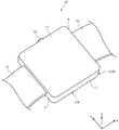
도 1은 일 실시예에 따른 예시적인 전자 디바이스의 전방 사시도이다.
도 2는 일 실시예에 따른 예시적인 전자 디바이스의 개략도이다.
도 3은 일 실시예에 따른 전자 디바이스 내의 예시적인 무선 회로부의 도면이다.
도 4는 일 실시예에 따른, 전자 디바이스의 후면을 통해 무선 신호들을 전달하는 안테나를 갖는 예시적인 전자 디바이스의 측단면도이다.
도 5는 일 실시예에 따른, 디바이스의 후방에 있는 안테나 및 사용자의 손목이 디바이스로부터 멀리 전자기 에너지를 어떻게 유도할 수 있는지를 보여주는 예시적인 전자 디바이스의 측단면도이다.
도 6은 일 실시예에 따른, 안테나 성능 정보를 수집하고 안테나에 대한 임피던스 매칭 회로를 조정하는 데 사용될 수 있는 예시적인 회로부의 도면이다.
도 7은 일 실시예에 따른, 상이한 안테나 로딩 조건들을 보상하기 위해 조정가능한 무선 회로부를 갖는 전자 디바이스를 동작시킬 때 포함될 수 있는 예시적인 단계들의 흐름도이다.
도 8은 일 실시예에 따른, 상이한 안테나 로딩 조건들을 보상하기 위해 임피던스 매칭 회로를 조정할지 여부를 결정할 때 전자 디바이스에 의해 수행될 수 있는 예시적인 단계들의 흐름도이다.
도 9 및 도 10은 일 실시예에 따른, 상이한 안테나 로딩 조건들을 보상하기 위해 임피던스 매칭 회로를 조정할 때 전자 디바이스에 의해 수행될 수 있는 예시적인 단계들의 흐름도들이다.
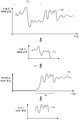
도 11은 일 실시예에 따른 임피던스 매칭 회로를 조정할지 여부를 결정하기 위해 처리될 수 있는, 전자 디바이스에 의해 수집된 수신 신호 강도 정보의 예시적인 플롯이다.
도 12는 일 실시예에 따른, 예시적인 전자 디바이스에 의해 수집된 수신 신호 강도 정보가, 임피던스 매칭 회로를 조정할지 여부를 결정하기 위해 어떻게 필터링되고 미리결정된 수신 신호 강도 패턴들과 비교될 수 있는지를 보여주는 도면이다.
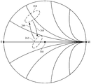
도 13은 일 실시예에 따른 상이한 안테나 로딩 조건들 하에서 동작될 때의 전자 디바이스 내의 안테나의 동작과 연관된 예시적인 임피던스들을 보여주는 스미스 차트(Smith chart)이다.
도 14는 일 실시예에 따른 상이한 임피던스 매칭 회로 설정들 하에서 동작할 때 안테나에 의해 나타날 수 있는 예시적인 안테나 주파수 응답들의 그래프이다.1 is a front perspective view of an exemplary electronic device according to one embodiment.
2 is a schematic diagram of an exemplary electronic device according to one embodiment.
3 is a drawing of an exemplary wireless circuitry in an electronic device according to one embodiment.
4 is a side cross-sectional view of an exemplary electronic device having an antenna that transmits radio signals through the back surface of the electronic device, according to one embodiment.
5 is a side cross-sectional view of an exemplary electronic device showing an antenna at the rear of the device and how a user's wrist can induce electromagnetic energy away from the device, according to one embodiment, in accordance with one embodiment.
6 is a drawing of an exemplary circuit portion that may be used to collect antenna performance information and adjust the impedance matching circuit for the antenna, in accordance with one embodiment.
7 is a flow diagram of exemplary steps that may be included in operating an electronic device having adjustable wireless circuitry to compensate for different antenna loading conditions, in accordance with one embodiment.
8 is a flow diagram of exemplary steps that may be performed by an electronic device in determining whether to tune an impedance matching circuit to compensate for different antenna loading conditions, in accordance with one embodiment.
9 and 10 are flow diagrams of exemplary steps that may be performed by an electronic device when adjusting an impedance matching circuit to compensate for different antenna loading conditions, in accordance with one embodiment.
FIG. 11 is an exemplary plot of received signal strength information collected by an electronic device, which may be processed to determine whether to adjust an impedance matching circuit in accordance with an embodiment.
12 illustrates how received signal strength information collected by an exemplary electronic device, in accordance with one embodiment, is filtered to determine whether to tune the impedance matching circuit and which can be compared to predetermined received signal strength patterns Fig.
13 is a Smith chart showing exemplary impedances associated with operation of an antenna in an electronic device when operated under different antenna loading conditions according to an embodiment.
14 is a graph of exemplary antenna frequency responses that may be exhibited by an antenna when operating under different impedance matching circuit configurations in accordance with one embodiment.
도 1의 전자 디바이스(10)와 같은 전자 디바이스에는 무선 통신 회로부가 제공될 수 있다. 무선 통신 회로부는 다수의 무선 통신 대역에서의 무선 통신을 지원하는 데 사용될 수 있다.An electronic device such as the
전자 디바이스(10)는, 랩톱 컴퓨터와 같은 컴퓨팅 디바이스, 임베디드 컴퓨터를 포함하는 컴퓨터 모니터, 태블릿 컴퓨터, 셀룰러 전화, 미디어 플레이어, 또는 다른 핸드헬드 또는 휴대용 전자 디바이스, 더 작은 디바이스, 예컨대 손목시계 디바이스, 펜던트(pendant) 디바이스, 헤드폰 또는 이어피스(earpiece) 디바이스, 안경 또는 사용자의 머리에 착용되는 다른 장비에 임베딩된 디바이스, 또는 다른 웨어러블(wearable) 또는 소형 디바이스, 텔레비전, 임베디드 컴퓨터를 포함하지 않는 컴퓨터 디스플레이, 게이밍 디바이스, 내비게이션 디바이스, 디스플레이를 구비한 전자 장비가 키오스크(kiosk) 또는 자동차 내에 장착되어 있는 시스템과 같은 임베디드 시스템, 이러한 디바이스들 중 둘 이상의 디바이스들의 기능을 구현하는 장비, 또는 다른 전자 장비일 수 있다. 도 1의 예시적인 구성에서, 디바이스(10)는 손목시계와 같은 웨어러블 디바이스이다. 원하는 경우, 디바이스(10)를 위한 다른 구성들이 사용될 수 있다. 도 1의 예는 단지 예시일 뿐이다.The
도 1의 예에서, 디바이스(10)는 디스플레이(14)와 같은 디스플레이를 포함한다. 디스플레이(14)는 하우징(12)과 같은 하우징 내에 장착될 수 있다. 때때로 인클로저 또는 케이스로 지칭될 수 있는 하우징(12)은 플라스틱, 유리, 세라믹, 섬유 복합재, 금속(예컨대, 스테인레스강, 금, 은, 알루미늄 등), 다른 적합한 재료들, 또는 이들 재료 중 임의의 둘 이상의 조합으로 형성될 수 있다. 하우징(12)은, 하우징(12)의 일부 또는 전부가 단일 구조체로서 기계가공되거나 성형되는 일체형 구성을 사용하여 형성될 수 있거나, 또는 다수의 구조체(예컨대, 내부 프레임 구조체, 외부 하우징 표면들을 형성하는 하나 이상의 구조체 등)를 사용하여 형성될 수 있다. 하우징(12)은 측벽들(12W)과 같은 금속 측벽들, 또는 다른 재료들로 형성된 측벽들을 가질 수 있다. 측벽들(12W)을 형성하는 데 사용될 수 있는 금속 재료들의 예들은 스테인레스강, 알루미늄, 은, 금, 금속 합금, 또는 임의의 다른 원하는 전도성 재료를 포함한다.In the example of Figure 1, the
디스플레이(14)는 디바이스(10)의 전면에 형성될 수 있다. 하우징(12)은 디바이스(10)의 전면에 대향하는 후방 벽(12R)과 같은 후방 하우징 벽을 가질 수 있다. 후방 하우징 벽(12R)은 디바이스(10)의 후면을 형성할 수 있다. 하우징 측벽들(12W)은 디바이스(10)의 주변부를 둘러쌀 수 있다(예를 들어, 하우징 측벽들(12W)은 디바이스(10)의 주변 에지들 둘레로 연장될 수 있다). 후방 하우징 벽(12R)은 유전체로 형성될 수 있다. 후방 하우징 벽(12R)을 형성하는 데 사용될 수 있는 유전체 재료들의 예들은 플라스틱, 유리, 사파이어, 세라믹, 목재, 중합체, 이들 재료의 조합들, 또는 임의의 다른 원하는 유전체들을 포함한다. 후방 하우징 벽(12R) 및/또는 디스플레이(14)는 디바이스(10)의 (예를 들어, 도 1의 x-축에 평행한) 길이 및 (예를 들어, y-축에 평행한) 폭의 일부 또는 전부에 걸쳐 연장될 수 있다. 하우징 측벽(12W)은 (예를 들어, z-축에 평행한) 디바이스(10)의 높이의 일부 또는 전부에 걸쳐 연장될 수 있다.The
디스플레이(14)는, 전도성 용량성 터치 센서 전극(conductive capacitive touch sensor electrode)들의 층 또는 다른 터치 센서 컴포넌트들(예컨대, 저항성 터치 센서 컴포넌트, 음향 터치 센서 컴포넌트, 힘 기반 터치 센서 컴포넌트, 광 기반 터치 센서 컴포넌트 등)을 통합하는 터치 스크린 디스플레이일 수 있거나, 또는 터치 감응형이 아닌 디스플레이일 수 있다. 용량성 터치 스크린 전극들은 인듐 주석 산화물 패드들의 어레이 또는 다른 투명 전도성 구조체들로 형성될 수 있다.The
디스플레이(14)는 액정 디스플레이(LCD) 컴포넌트들로 형성된 디스플레이 픽셀들의 어레이, 전기 영동 디스플레이 픽셀들의 어레이, 플라즈마 디스플레이 픽셀들의 어레이, 유기 발광 다이오드 디스플레이 픽셀들의 어레이, 전기습윤 디스플레이 픽셀들의 어레이, 또는 다른 디스플레이 기술들에 기초한 디스플레이 픽셀들을 포함할 수 있다.
디스플레이(14)는 디스플레이 커버 층을 사용해 보호될 수 있다. 디스플레이 커버 층은 투명 재료, 예컨대 유리, 플라스틱, 사파이어 또는 다른 결정질 유전체 재료들, 세라믹, 또는 다른 투명 재료들로 형성될 수 있다. 디스플레이 커버 층은 예를 들어, 디바이스(10)의 길이 및 폭의 실질적으로 전부에 걸쳐 연장될 수 있다.The
디바이스(10)는 버튼(18)과 같은 버튼들을 포함할 수 있다. 디바이스(10)에는 임의의 적합한 수의 버튼들이 있을 수 있다(예를 들어, 단일 버튼, 하나 초과의 버튼, 2개 이상의 버튼, 5개 이상의 버튼 등). 버튼들은 (예로서) 하우징(12) 내의(예를 들어, 측벽(12W) 또는 후방 벽(12R) 내의) 개구들 내에 또는 디스플레이(14) 내의 개구 내에 위치될 수 있다. 버튼들은 회전식 버튼, 슬라이딩 버튼, 이동가능한 버튼 부재를 누름으로써 작동되는 버튼, 이들의 조합들 등일 수 있다. 버튼(18)과 같은 버튼들에 대한 버튼 부재들은 금속, 유리, 플라스틱, 또는 다른 재료들로 형성될 수 있다. 버튼(18)은 디바이스(10)가 손목시계 디바이스인 시나리오들에서 때때로 크라운으로서 지칭될 수 있다.The
디바이스(10)는, 원하는 경우, 스트랩(16)과 같은 스트랩에 결합될 수 있다. 스트랩(16)은 (예로서) 사용자의 손목에 대해 디바이스(10)를 유지하는 데 사용될 수 있다. 도 1의 예들에서, 스트랩(16)은 디바이스(10)의 대향하는 측면들(8)에 연결된다. 디바이스(10)의 측면들(8) 상의 하우징 벽들(12W)은 스트랩(16)을 하우징(12)에 고정하기 위한 부착 구조체들(예를 들어, 러그(lug) 또는 다른 부착 메커니즘)을 포함할 수 있다. 스트랩(16)은 임의의 원하는 재료들(예를 들어, 금속 재료, 유전체 재료, 또는 금속 및 유전체 재료들의 조합들)로 형성될 수 있다. 예를 들어, 스트랩(16) 내의 금속 재료들은 스테인레스강, 알루미늄, 은, 금, 금속 합금, 또는 임의의 다른 원하는 전도성 재료를 포함할 수 있다. 스트랩(16) 내의 유전체 재료들은 플라스틱, 중합체, 세라믹, 가죽, 고무, 천 또는 다른 직물, 유리, 또는 임의의 다른 원하는 유전체 재료들을 포함할 수 있다.The
원하는 경우, 스트랩(16)은 착탈식일 수 있다. 예를 들어, 사용자는 스트랩(16)을, 유사하거나 상이한 재료들을 갖는 상이한 스트랩으로 대체할 수 있다. 원하는 경우, 스트랩(16)은 조정가능할 수 있다. 예를 들어, 스트랩(16)은 클래스프(clasp), 버클(buckle), 또는 사용자가 스트랩(16)의 길이를 조정하도록 그리고/또는 사용자가 디바이스(10)를 착용하는 동안 스트랩(16)이 사용자의 손목 상에서 얼마나 타이트할지 조정하도록 허용하는 다른 조정가능한 구조체들을 포함할 수 있다. 스트랩을 포함하지 않는 구성도 디바이스(10)에 사용될 수 있다.If desired, the
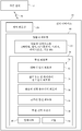
디바이스(10)에서 사용될 수 있는 예시적인 컴포넌트들을 도시하는 개략도가 도 2에 도시된다. 도 2에 도시된 바와 같이, 디바이스(10)는 저장 및 처리 회로부(28)와 같은 제어 회로부를 포함할 수 있다. 저장 및 처리 회로부(28)는 하드 디스크 드라이브 저장소, 비휘발성 메모리(예컨대, 플래시 메모리, 또는 솔리드 스테이트 드라이브(solid state drive)를 형성하도록 구성된 다른 전기적 프로그램가능 판독 전용 메모리), 휘발성 메모리(예컨대, 정적 또는 동적 랜덤 액세스 메모리) 등과 같은 저장소를 포함할 수 있다. 저장 및 처리 회로부(28) 내의 처리 회로부는 디바이스(10)의 동작을 제어하는 데 사용될 수 있다. 이러한 처리 회로부는 하나 이상의 마이크로프로세서, 마이크로제어기, 디지털 신호 프로세서, 응용 주문형 집적 회로 등에 기초할 수 있다.A schematic diagram illustrating exemplary components that may be used in the
저장 및 처리 회로부(28)는 인터넷 브라우징 애플리케이션, VOIP(voice-over-internet-protocol) 전화 통화 애플리케이션, 이메일 애플리케이션, 미디어 재생 애플리케이션, 운영 체제 기능들 등과 같은 소프트웨어를 디바이스(10) 상에서 실행하는 데 사용될 수 있다. 외부 장비와의 상호작용을 지원하기 위해, 저장 및 처리 회로부(28)는 통신 프로토콜을 구현하는 데 사용될 수 있다. 저장 및 처리 회로부(28)를 사용하여 구현될 수 있는 통신 프로토콜들은 인터넷 프로토콜, 무선 로컬 영역 네트워크 프로토콜(예컨대, IEEE 802.11 프로토콜 -- 때때로 와이파이®로 지칭됨), 블루투스® 프로토콜과 같은 다른 단거리 무선 통신 링크를 위한 프로토콜, 셀룰러 전화 프로토콜, MIMO 프로토콜, 안테나 다이버시티 프로토콜 등을 포함한다.The storage and
입출력 회로부(44)는 입출력 디바이스들(32)을 포함할 수 있다. 입출력 디바이스들(32)은 데이터가 디바이스(10)에 공급되게 하기 위해, 그리고 데이터가 디바이스(10)로부터 외부 디바이스들로 제공되게 하기 위해 사용될 수 있다. 입출력 디바이스들(32)은 사용자 인터페이스 디바이스, 데이터 포트 디바이스, 및 다른 입출력 컴포넌트들을 포함할 수 있다. 예를 들어, 입출력 디바이스들(32)은 터치 스크린, 터치 센서 기능이 없는 디스플레이, 버튼, 스크롤 휠, 터치 패드, 키 패드, 키보드, 마이크로폰, 카메라, 버튼, 스피커, 상태 표시기, 광원, 오디오 잭 및 다른 오디오 포트 컴포넌트, 디지털 데이터 포트 디바이스, 광 센서, 발광 다이오드, 모션 센서(가속도계), 정전용량 센서, 근접 센서, 자기 센서, 힘 센서(예컨대, 디스플레이에 가해진 압력을 검출하기 위해 디스플레이에 결합된 힘 센서) 등을 포함할 수 있다.The input /
도 2에 도시된 바와 같이, 전자 디바이스(10)는 무선 링크(54)와 같은 무선 링크들을 통해 외부 장비(52)와 무선으로 통신할 수 있다. 외부 장비(52)는 셀룰러 전화 네트워크 기지국, 무선 로컬 영역 네트워크 장비(예컨대, 무선 라우터 및/또는 무선 액세스 포인트), 피어 디바이스(peer device), 셀룰러 전화 또는 무선 헤드셋과 같은 다른 휴대용 전자 디바이스, 및 다른 외부 장비를 포함할 수 있다. 링크(54)는 셀룰러 전화 링크, 무선 로컬 영역 네트워크 링크, 또는 다른 유형들의 무선 통신을 사용하여 지원되는 통신 링크일 수 있다.As shown in FIG. 2, the
입출력 회로부(44)는 무선 회로부(34)를 포함할 수 있다. 무선 회로부(34)는 무선 전력 어댑터로부터 무선으로 전송된 전력을 수신하기 위한 무선 전력 수신기(48) 및 코일(50)을 포함할 수 있다. 무선 통신을 지원하기 위해, 무선 회로부(34)는 하나 이상의 집적 회로로 형성된 무선 주파수(RF) 송수신기 회로부, 전력 증폭기 회로부, 저잡음 입력 증폭기, 수동 RF 컴포넌트, 안테나들(40)과 같은 하나 이상의 안테나, 전송 라인, 및 RF 무선 신호들을 처리하기 위한 다른 회로부를 포함할 수 있다. 무선 신호들은 또한 광을 이용하여(예컨대, 적외선 통신을 이용하여) 전송될 수 있다.The input /
무선 회로부(34)는 다양한 무선 주파수 통신 대역을 처리하기 위한 무선 주파수 송수신기 회로부(56)를 포함할 수 있다. 예를 들어, 회로부(34)는 송수신기 회로부(36, 38, 42, 46)를 포함할 수 있다. 송수신기 회로부(36)는 와이파이®(IEEE 802.11) 통신을 위한 2.4 ㎓ 및 5 ㎓ 대역들을 처리할 수 있고 2.4 ㎓ 블루투스® 통신 대역을 처리할 수 있는 무선 로컬 영역 네트워크 송수신기 회로부일 수 있다. 회로부(34)는, (예로서) 700 내지 960 ㎒의 낮은 통신 대역, 1400 ㎒ 또는 1500 ㎒ 내지 2170 ㎒의 중간 대역(예를 들어, 1700 ㎒에서 피크를 갖는 중간 대역), 및 2170 또는 2300 내지 2700 ㎒의 높은 대역(예를 들어, 2400 ㎒에서 피크를 갖는 높은 대역) 또는 700 ㎒와 2700 ㎒ 사이의 다른 통신 대역들과 같은 주파수 범위들, 또는 다른 적합한 주파수들에서의 무선 통신을 처리하기 위한 셀룰러 전화 송수신기 회로부(38)를 사용할 수 있다. 회로부(38)는 음성 데이터 및 비음성 데이터를 처리할 수 있다. 무선 통신 회로부(34)는, 원하는 경우, 다른 단거리 및 장거리 무선 링크들을 위한 회로부를 포함할 수 있다. 예를 들어, 무선 통신 회로부(34)는 60 ㎓ 송수신기 회로부, 텔레비전 및 라디오 신호들을 수신하기 위한 회로부, 페이징 시스템 송수신기, 근거리 통신(NFC) 송수신기 회로부(46)(예를 들어, 13.56 ㎒ 또는 다른 적합한 주파수에서 동작하는 NFC 송수신기) 등을 포함할 수 있다. 무선 회로부(34)는 1575 ㎒에서 GPS 신호들을 수신하기 위한 또는 다른 위성 포지셔닝 데이터를 처리하기 위한 글로벌 포지셔닝 시스템(GPS) 수신기 회로부(42)와 같은 위성 항법 시스템 회로부를 포함할 수 있다. 와이파이® 및 블루투스® 링크들 및 다른 단거리 무선 링크들에서, 무선 신호들은 전형적으로 수십 또는 수백 피트에 걸쳐 데이터를 전달하는 데 이용된다. 셀룰러 전화 링크들 및 다른 장거리 링크들에서, 무선 신호들은 전형적으로 수천 피트 또는 마일에 걸쳐 데이터를 전달하는 데 이용된다.The
무선 회로부(34)는 안테나들(40)을 포함할 수 있다. 안테나들(40)은 임의의 적합한 안테나 유형들을 이용하여 형성될 수 있다. 예를 들어, 안테나들(40)은 루프 안테나 구조체, 패치 안테나 구조체, 역-F 안테나 구조체, 슬롯 안테나 구조체, 평면형 역-F 안테나 구조체, 나선형 안테나 구조체, 모노폴 안테나 구조체, 다이폴 안테나 구조체, 이들 설계의 하이브리드들 등으로부터 형성되는 공진 요소들을 갖는 안테나들을 포함할 수 있다. 상이한 유형의 안테나들이 상이한 대역들 또는 대역들의 조합들에 대해 사용될 수 있다. 예를 들면, 하나의 유형의 안테나는 로컬 무선 링크 안테나를 형성하는 데 사용될 수 있는 반면에, 다른 유형의 안테나는 원격 무선 링크 안테나를 형성하는 데 사용된다. 원하는 경우, 단일 안테나를 사용하여 둘 이상의 상이한 통신 대역을 처리함으로써 디바이스(10) 내에서 공간이 보전될 수 있다. 예를 들어, 디바이스(10) 내의 단일 안테나(40)는 2.4 ㎓에서의 와이파이® 또는 블루투스® 통신 대역, 1575 ㎒에서의 GPS 통신 대역, 및/또는 700 내지 960 ㎒, 1400 내지 2170 ㎒, 및 2170 내지 2700 ㎒에서의 하나 이상의 셀룰러 전화 대역과 같은 셀룰러 전화 통신 대역에서의 통신을 처리하는 데 사용될 수 있다.The
그러나, 실제로, 안테나에 요구되는 일반적인 크기는 동작을 위한 원하는 주파수가 감소함에 따라(즉, 대응하는 파장이 증가함에 따라) 증가한다. 또한, 디바이스(10)와 같은 콤팩트한 전자 디바이스들에서 공간은 확보하기가 힘들다(예를 들어, 특히 보다 작고 보다 미적으로 만족스러운 디바이스 폼 팩트에 대한 요구가 증가함에 따라). 주의를 기울이지 않으면, 모든 관심 통신 대역에서, 특히 700 내지 960 ㎒에서의 낮은 대역 셀룰러 전화 주파수들과 같은 비교적 낮은 주파수들(즉, 비교적 긴 파장들)에 대해, 만족스러운 안테나 커버리지를 콤팩트한 전자 디바이스들에 제공할 수 있는 것은 어려울 수 있다.However, in practice, the general size required for the antenna increases as the desired frequency for operation decreases (i. E., The corresponding wavelength increases). Also, in compact electronic devices such as
도 3은 무선 회로부(34) 내의 송수신기 회로부(56)가 경로(60)와 같은 경로들을 사용하여 안테나 구조체들(40)에 어떻게 결합될 수 있는지를 보여주는 도면이다. 무선 회로부(34)는 제어 회로부(28)에 결합될 수 있다. 제어 회로부(28)는 입출력 디바이스들(32)에 결합될 수 있다. 입출력 디바이스들(32)은 디바이스(10)로부터의 출력을 공급할 수 있고 디바이스(10)의 외부에 있는 소스들로부터의 입력을 수신할 수 있다.3 is a diagram illustrating how the
관심 통신 주파수들을 커버하는 능력을 안테나 구조체들(40)에 제공하기 위해, 안테나 구조체들(40)은 필터 회로부(예컨대, 하나 이상의 수동 필터 및/또는 하나 이상의 튜닝가능한 필터 회로)와 같은 회로부를 구비할 수 있다. 커패시터들, 인덕터들, 및 저항기들과 같은 개별 컴포넌트들이 필터 회로부 내에 통합될 수 있다. 용량성 구조체들, 유도성 구조체들, 및 저항성 구조체들이, 또한, 패턴화된 금속 구조체들(예컨대, 안테나의 일부)로부터 형성될 수 있다. 원하는 경우, 안테나 구조체들(40)은 관심 통신 대역들에 걸쳐 안테나들을 튜닝하기 위한 튜닝가능한 컴포넌트들(62)과 같은 조정가능한 회로들을 구비할 수 있다. 튜닝가능한 컴포넌트들(62)은 튜닝가능한 인덕터들, 튜닝가능한 커패시터들, 또는 다른 튜닝가능한 컴포넌트들을 포함할 수 있다. 이들과 같은 튜닝가능한 컴포넌트들은 고정된 컴포넌트들의 스위치들 및 네트워크들, 연관된 분산된 커패시턴스들 및 인덕턴스들을 생성하는 분산형 금속 구조체들, 가변 커패시턴스 및 인덕턴스 값들을 생성하기 위한 가변 솔리드 스테이트 디바이스들, 튜닝가능한 필터들, 또는 다른 적합한 튜닝가능한 구조체들에 기초할 수 있다.To provide the
디바이스(10)의 동작 동안, 제어 회로부(28)는 인덕턴스 값들, 커패시턴스 값들, 또는 튜닝가능한 컴포넌트들(62)과 연관된 다른 파라미터들을 조정하는 제어 신호들을 경로(64)와 같은 하나 이상의 경로 상에 발생(issue)시킴으로써, 원하는 통신 대역들을 커버하도록 안테나 구조체들(40)을 튜닝할 수 있다.During operation of
경로(60)는 하나 이상의 무선 주파수 전송 라인을 포함할 수 있다. 예로서, 도 3의 신호 경로(60)는 경로들(66, 68)과 같은 제1 및 제2 전도성 경로들을 각각 갖는 전송 라인일 수 있다. 경로(66)는 양의 신호 라인일 수 있고 경로(68)는 접지 신호 라인일 수 있다. 라인들(66, 68)은 (예로서) 동축 케이블, 스트립라인 전송 라인, 및/또는 마이크로스트립 전송 라인의 부분들을 형성할 수 있다. 인덕터들, 저항기들, 및 커패시터들과 같은 컴포넌트들로 형성된 매칭 네트워크는 안테나 구조체들(40)의 임피던스를 전송 라인(60)의 임피던스에 매칭시키는 데 사용될 수 있다. 매칭 네트워크 컴포넌트들은 개별 컴포넌트들(예컨대, 표면 실장 기술 컴포넌트들)로서 제공될 수 있거나, 또는 하우징 구조체, 인쇄 회로 기판 구조체, 플라스틱 지지부 상의 트레이스 등으로부터 형성될 수 있다. 매칭 네트워크 컴포넌트들은 예를 들어, 라인(60) 상에 개재될 수 있다. 매칭 네트워크 컴포넌트들은 원하는 경우, 제어 회로부(28)로부터 수신된 제어 신호들을 사용하여 조정될 수 있다. 이들과 같은 컴포넌트들은 또한 안테나 구조체들(40) 내의 필터 회로부를 형성하는 데 사용될 수 있다.The
전송 라인(60)은 안테나(40)에 대한 안테나 공진 요소 및 접지에 직접 연결될 수 있거나, 또는 안테나(40)에 대한 공진 요소에 간접적으로 피드(feed)하는 데 사용되는 근거리-결합(near-field-coupled) 안테나 피드 구조체들에 결합될 수 있다. 일례로서, 안테나 구조체들(40)은 역-F 안테나, 루프 안테나, 패치 안테나, 슬롯 안테나, 또는 단자(70)와 같은 양의 안테나 피드 단자 및 접지 안테나 피드 단자(72)와 같은 접지 안테나 피드 단자를 구비한 안테나 피드부를 갖는 다른 안테나를 형성할 수 있다. 양의 전송 라인 전도체(66)는 양의 안테나 피드 단자(70)에 결합될 수 있고, 접지 전송 라인 전도체(68)는 접지 안테나 피드 단자(72)에 결합될 수 있다. 원하는 경우, 안테나(40)는 근거리 결합을 사용하여 간접적으로 피드되는 안테나 공진 요소를 포함할 수 있다. 근거리 결합 배열에서, 전송 라인(60)은 안테나 공진 요소와 같은 안테나 구조체들에 간접적으로 피드하는 데 사용되는 근거리-결합 안테나 피드 구조체에 결합된다. 이러한 예는 단지 예시일 뿐이며, 일반적으로, 임의의 원하는 안테나 피드 배열이 사용될 수 있다.The
도 4는 안테나(40)가 디바이스(10) 내에서 어떻게 형성될 수 있는지를 보여주는 예시적인 디바이스(10)의 측단면도이다. 도 4의 페이지의 평면은 예를 들어, 도 1의 X-Z 평면일 수 있다.4 is a side cross-sectional view of an
도 4에 도시된 바와 같이, 디바이스(10)는 디바이스(10)의 후면으로부터 전면으로 연장되는 전도성 하우징 측벽들(12W)을 가질 수 있다. 디스플레이(14)는 디바이스(10)의 전면을 형성할 수 있는 반면에, 유전체 후방 하우징 벽(12R)은 디바이스(10)의 후면을 형성한다. 금속 하우징 측벽들(12W)은 원하는 경우 안테나(40)에 대한 안테나 접지의 일부분을 형성하는 데 사용될 수 있다.As shown in FIG. 4, the
디스플레이(14)는 디스플레이 커버 층(86) 및 디스플레이 모듈(84)을 포함할 수 있다. 디스플레이 모듈(84)은 터치 센서, 픽셀, 또는 디스플레이 커버 층(86)을 통해 광을 방출하는 다른 발광 컴포넌트들과 같은 능동 디스플레이 컴포넌트들을 포함할 수 있다. 디스플레이 커버 층(86)은 디바이스(10)의 길이 및 폭의 일부 또는 실질적으로 전부에 걸쳐 연장될 수 있다. 디스플레이 커버 층(86)은 (예를 들어, 광을 사용자가 볼 수 있도록) 디스플레이 모듈(172)에 의해 방출된 광을 통과시키는 투명 부분을 포함할 수 있다. 원하는 경우, 잉크 층과 같은 불투명 마스킹 층이, 디바이스(10)의 내부 컴포넌트들을 시야로부터 숨기기 위해 디스플레이 모듈(84)을 넘어서 연장되는 디스플레이 커버 층(86)의 부분을 따라 형성될 수 있다.
스트랩(16)은 대응하는 부착 구조체들(88)을 사용하여 하우징 측벽들(12W)에 고정될 수 있다. 부착 구조체들(88)은 러그, 스프링 구조체, 또는 임의의 다른 원하는 부착 메커니즘들을 포함할 수 있다. 스트랩(16)은 임의의 원하는 재료들(예를 들어, 금속 재료, 유전체 재료, 또는 금속 및 유전체 재료들의 조합들)을 사용하여 형성될 수 있다. 원하는 경우, 스트랩(16)은 (예를 들어, 디바이스(10)의 사용자가 유사한 또는 상이한 재료들을 갖는 상이한 스트랩들 중에서 교체할 수 있도록) 부착 구조체들(88)로부터 제거될 수 있다.The
디바이스(10)는 인쇄 회로 기판(80)과 같은 인쇄 회로 기판 구조체들을 포함할 수 있다. 인쇄 회로 기판(80)은 강성 인쇄 회로 기판, 가요성 인쇄 회로 기판일 수 있거나, 또는 가요성 및 강성 인쇄 회로 기판 구조체들 둘 다를 포함할 수 있다. 인쇄 회로 기판(80)은 때때로 본 명세서에서 메인 로직 보드(80)로 지칭될 수 있다. 전기 컴포넌트들(82)은 메인 로직 보드(80)에 장착될 수 있다. 전기 컴포넌트들(82)은 예를 들어, 송수신기 회로부(56), 하나 이상의 입출력 디바이스(32), 제어 회로부(28)(도 2)의 일부 또는 전부, 하우징(12)의 부분들, 또는 임의의 다른 원하는 컴포넌트들을 포함할 수 있다. 메인 로직 보드(80)는 전도성 층(76)과 같은 하나 이상의 전도성 층을 포함할 수 있다. 전도성 층(76)은 예를 들어, 안테나(40)에 대한 안테나 접지의 일부분을 형성할 수 있다. 따라서 전도성 층(76)은 본 명세서에서 때때로 접지된 층(76), 접지 층(76), 접지 전도체(76), 또는 접지된 전도체(76)로 지칭될 수 있다.The
전도성 층(76)은, 원하는 경우, 금속 하우징 측벽들(12W)에 단락될(접지될) 수 있다(예를 들어, 안테나(40)에 대한 안테나 접지는 전도성 층(76) 및 금속 하우징 측벽들(12W)을 포함할 수 있다). 전도성 층(76)은 금속 포일, 스탬핑된 시트 금속, 메인 로직 보드(80)의 표면 상에 패턴화된 전도성 트레이스들, 메인 로직 보드(80)에 장착된 가요성 인쇄 회로 상의 전도성 트레이스, 금속 하우징 부분들을 사용하여, 또는 임의의 다른 원하는 전도성 구조체들로 형성될 수 있다. 원하는 경우, 전도성 층(76)은 메인 로직 보드(80) 내에 형성될(임베딩될) 수 있다(예를 들어, 전도성 층(76)은 로직 보드(80)의 유전체 층들 사이에 스택될 수 있다). 다른 적합한 배열에서, 전도성 층(76)은 생략될 수 있다.The
도 4에 도시된 바와 같이, 후방 하우징 벽(12R)은 디바이스(10)의 길이 및 폭의 실질적으로 전부에 걸쳐 연장될 수 있다. 후방 하우징 벽(12R)은 임의의 원하는 유전체 재료로 형성될 수 있다. 예를 들어, 후방 하우징 벽(12R)은 플라스틱, 유리, 사파이어, 세라믹, 목재, 중합체, 이들 재료의 조합들, 또는 임의의 다른 원하는 유전체들로 형성될 수 있다. 후방 하우징 벽(12R)은 광학적으로 불투명하거나 광학적으로 투명할 수 있거나, 또는 광학적으로 불투명한 부분 및 광학적으로 투명한 부분 둘 모두를 포함할 수 있다.As shown in FIG. 4, the
안테나(40)는 안테나 구조체들(74)을 포함할 수 있다. 안테나 구조체들(74)은 예를 들어, 안테나(40)에 대한 안테나 공진 요소의 일부 또는 전부일 수 있다(예를 들어, 역-F 안테나 공진 요소 아암, 평면형 역-F 안테나 공진요소, 패치 안테나 공진 요소, 다이폴 안테나 공진 요소, 모노폴 안테나 공진 요소 등). 하나의 적합한 실시예에서, 안테나 공진 요소(74)는 유전체 하우징 벽(12R)의 내부 표면 상에 직접 패턴화되는 전도성 트레이스들로 형성될 수 있다(예를 들어, 패턴화된 전도성 트레이스들은 유전체 하우징 벽(12R)의 내부 표면과 직접 접촉할 수 있다). 원하는 경우, 안테나 공진 요소(74)는 전도성 포일, 또는 후방 하우징 벽(12R)과 직접 접촉하여 배치되는 다른 전도성 구조체들을 사용하여 형성될 수 있다. 다른 적합한 배열에서, 안테나 공진 요소(74)는 가요성 인쇄 회로 기판, 또는 후방 하우징 벽(12R) 위에(예를 들어, 그로부터 수직으로 이격되고 중첩되어) 또는 그와 직접 접촉하여 위치되는 다른 유전체 기판 상의 전도성 트레이스들로 형성될 수 있다. 안테나 공진 요소 트레이스들(74)은 임의의 원하는 전도성 재료(예를 들어, 알루미늄, 구리, 금속 합금, 스테인레스강, 금 등)를 사용하여 형성될 수 있다.The
유전체 재료들을 사용하여 후방 하우징 벽(12R)이 형성되는 도 4의 예는 단지 예시일 뿐이다. 원하는 경우, 디바이스(10)의 후방 하우징 벽은 전도성 및 유전체 재료들의 조합을 포함할 수 있다. 예를 들어, 후방 하우징 벽의 일부분은 금속으로 형성될 수 있는 반면에, 후방 하우징 벽의 다른 부분은 유전체로 형성된다(예를 들어, 유전체로 형성된 후방 하우징 벽의 부분은 디바이스(10)의 길이 및 폭의 일부에 걸쳐 연장될 수 있지만 그 전부에 걸쳐 연장되지는 않는다). 후방 하우징 벽의 유전체 부분은 예를 들어, 후방 하우징 벽의 전도성 부분 내의 유전체 윈도우(dielectric window)를 포함할 수 있다(예를 들어, 후방 하우징 벽은 후방 하우징 벽의 유전체 부분 또는 후방 하우징 벽의 유전체 부분을 둘러싸는 다른 구조체들에 대한 금속 프레임을 포함할 수 있다). 후방 하우징 벽은 원하는 경우 다수의 유전체 윈도우를 포함할 수 있다.The example of FIG. 4 in which the
안테나(40)의 양의 안테나 피드 단자(70)는 안테나(40)에 대한 무선 주파수 안테나 신호들을 피드하기 위해 안테나 공진 요소 트레이스들(74)의 일부분에 결합될 수 있다. 접지 안테나 피드 단자(72)는 안테나(40)에 대한 안테나 접지에 결합될 수 있다. 도 4의 예에서, 접지 안테나 피드 단자(72)는 금속 하우징 측벽(12W)에 결합된다. 원하는 경우, 접지 안테나 피드 단자(72)는 전도성 층(76) 또는 임의의 다른 접지된 구조체들에 결합될 수 있다. 원하는 경우, 안테나 공진 요소 트레이스들(74)의 하나 이상의 추가의 부분은 다른 전도성 경로들(도시되지 않음)을 사용해 안테나 접지(예를 들어, 하우징 벽(12W), 전도성 층(76), 및/또는 다른 접지된 구조체들)에 단락될 수 있다. 그러한 전도성 경로들은 예를 들어, 안테나(40)에 대한 복귀(단락) 경로를 형성할 수 있다(예를 들어, 안테나(40)가 역-F 안테나 또는 평면형 역-F 안테나인 시나리오들에서).The positive
안테나 공진 요소 트레이스들(74)이 후방 하우징 벽(12R) 상에 직접 패턴화되는 시나리오들에서, 후방 하우징 벽(12R)은 안테나 공진 요소(74)에 대한 기계적 지지 구조체 또는 캐리어 구조체로서의 역할을 할 수 있다. 안테나 공진 요소 트레이스들(74)은 유전체 후방 하우징 벽(12R)의 내부 표면의 형상에 순응할 수 있다. 도 4의 예에서, 유전체 후방 하우징 벽(12R)의 내부 표면은 (예를 들어, 벽(12R)의 내부 표면이 편평한 시나리오들에 비해 디바이스(10) 내의 컴포넌트들을 위한 총 용적을 증가시키기 위해) 약간 만곡된 형상을 갖는다. 따라서 안테나 공진 요소 트레이스들(74)은 후방 하우징 벽(12R)과 직접 접촉하는 만곡된 표면 내에 형성될 수 있다. 다른 적합한 배열에서, 안테나 공진 요소 트레이스들(74)은 후방 하우징 벽(12R)과 접촉하여 배치되거나 그 위에 적층되는 가요성 인쇄 회로 또는 다른 기판 상에 형성될 수 있다.In the scenarios in which the antenna resonant element traces 74 are patterned directly on the
안테나(40)는 후방 하우징 벽(12R)을 통해 무선 주파수 신호들을 수신 및/또는 전송할 수 있다. 안테나(40)에 의해 전송된 무선 주파수 신호들은 예를 들어, 전도성 층(76) 및 메인 로직 보드(80)에 의해 전기 컴포넌트들(82)로부터 차폐될 수 있다. 유사하게, 전도성 층(76) 및 메인 로직 보드(80)는 컴포넌트들(82)로부터 안테나(40)를 차폐시켜, 안테나(40)와 컴포넌트들(82) 사이의 전자기 간섭을 완화시킬 수 있다.The
원하는 경우, 다른 컴포넌트들(예를 들어, 광 센서, 근접 센서, 터치 센서 등과 같은 하나 이상의 센서(32))이 후방 하우징 벽(12R)에 장착될 수 있다. 예를 들어, 안테나 공진 요소 트레이스들(74)은 후방 하우징 벽(12R)에 장착되는 다른 컴포넌트들의 주변부를 둘러싸거나 그 주위에 형성될 수 있다. 하나의 적합한 배열에서, 코일(50)(도 2)이 유전체 후방 하우징 벽(12R)을 통해 무선 전력(예를 들어, 무선 충전 신호들)을 수신하기 위해 후방 하우징 벽(12R)과 접촉하여 배치될 수 있다. 이 시나리오에서, 안테나 공진 요소 트레이스들(74)은 후방 하우징 벽(12R)의 내부 표면에서 코일(50)을 둘러쌀 수 있다.If desired, other components (e.g., one or
후방 하우징 벽(12R)에 인접한 안테나(40)를 형성함으로써, 디바이스(10)의 수직 높이(H)는 (안테나(40)가 여전히 만족스러운 안테나 효율을 나타내게 하면서도) 안테나 공진 요소가 디바이스(10) 상의 다른 곳에 위치되는 시나리오들에서 가능하게 될 높이보다 더 짧을 수 있다. 일례로서, 수직 높이(H)는 11.4 mm 이하, 15 mm 미만, 8 내지 11.4 mm, 또는 임의의 다른 원하는 높이일 수 있으면서, 안테나(40)가 여전히 만족스러운 안테나 효율로 동작하게 할 수 있다. 디바이스(10)의 후면을 따라 안테나(40)를 형성하는 것은 또한 디스플레이(14)의 비활성 영역(화살표(I)에 의해 도시된 바와 같음)의 크기의 감소를 허용할 수 있는데, 이는 안테나(40)가, 신호들이 디스플레이 모듈(84)에 의해 차단될 것이라는 우려 없이, 무선 주파수 신호들을 디바이스(10)의 후면을 통해 전송할 수 있기 때문이다.By forming the
후방 하우징 벽(12R)을 따라 안테나(40)를 형성하는 것은 또한 700 내지 960 ㎒의 셀룰러 전화 대역에서의 주파수들과 같은 비교적 낮은 주파수들의 커버리지를 허용하기 위해 안테나 공진 요소(74)의 주변부가 충분히 크도록 허용할 수 있다. 일반적으로, 안테나(40)는 700 ㎒ 초과의 무선 주파수 신호들, 예컨대 IEEE 802.11 통신, 블루투스®, 및/또는 (일례로서) 주변부 안테나(40P)에 의해 처리될 수 있는 다른 무선 로컬 영역 네트워크 통신을 위한 2.4 ㎓ 및/또는 5 ㎓에서의 신호들, 저대역 셀룰러 전화 신호들(예를 들어, 700 ㎒ 내지 960 ㎒의 주파수들에서의 셀룰러 전화 통신), 중간 대역, 고대역, 및 960 내지 2700 ㎒에서의 셀룰러 전화 및 GPS 신호들과 같은 960 ㎒ 초과의 다른 대역들에서의 셀룰러 전화 신호들 및 GPS 신호들, IEEE 802.11 통신, 블루투스®, 및/또는 다른 무선 로컬 영역 네트워크 통신을 위한 2.4 ㎓ 및/또는 5 ㎓, 및 임의의 다른 원하는 대역들에서의 무선 주파수 신호들을 처리할 수 있다. 단일 안테나(40)를 사용하여 이들 대역 모두를 커버함으로써, 그렇지 않았으면 디바이스(10) 내의 추가의 안테나들에 의해 점유되었을 공간이 다른 전자 디바이스 컴포넌트들을 위해 사용되거나, 또는 안테나 효율을 희생시키지 않으면서 디바이스(10)의 크기(예를 들어, 도 4의 치수 H 및/또는 I)를 더욱 줄이기 위해 사용될 수 있다.The formation of the
실제로, 안테나(40)의 성능은 후방 하우징 벽(12R)에 인접한 외부 물체의 존재에 의해 최적화될 수 있다. 예를 들어, 사용자가 디바이스(10)를 착용하고 있을 때 후방 하우징 벽(12R)에 인접한 사용자의 손목(90)의 존재는 안테나(40)의 성능을 향상시킬 수 있다. 동작 동안, 안테나 공진 요소(74)는 후면(12R) 및 손목(90)의 표면들에 수직으로 배향되는 전기장(E)을 갖는 무선 주파수 신호들을 전송 및/또는 수신할 수 있다. 이들 신호는 때때로 손목(90)의 표면을 따라 그리고 외측으로 전파되는 표면파로 지칭될 수 있다(예를 들어, 안테나 공진 요소 트레이스들(74) 및 손목(90)은 표면파를 외측으로 지향시키는 도파관으로서의 역할을 할 수 있다).In practice, the performance of the
도 5는 안테나(40)에 의해 전송된 전자기 신호들이 사용자의 손목의 존재로 인해 어떻게 외측으로 전파될 수 있는지를 보여주는 측단면도이다. 도 5에 도시된 바와 같이, 윤곽선들(92)은 일정한 전기장 크기의 윤곽들을 나타낸다. 안테나(40)에 의해 발생된 전기장의 크기는 디바이스(10)와 손목(90) 사이의 공간에서 가장 높다. 신호들은 경로(98)에 의해 도시된 바와 같이, 디바이스(10)로부터 멀어지는 외측 방향으로 공진 요소 트레이스(74) 및 손목(90)의 표면을 따라 전파할 수 있다. 이는 안테나(40)가 손목(90)에 가깝게 위치되고 전형적으로 외부 통신 장비로부터 멀어지는 방향으로 향하더라도 신호들이 외부 통신 장비(예를 들어, 도 2의 장비(52))에 의해 적절히 수신되도록 할 수 있다. 실제로, 손목(90)의 존재는 손목(90)이 존재하지 않는 상황들에 비해 전자기파의 전파를 향상시키는 역할을 할 수 있다. 예를 들어, 안테나(40)에 의해 방출된 무선 주파수 신호들은 손목(90)의 부재 시 적절히 지향되지 않을 수 있어, 외부 장비와의 무선 링크 품질이 나쁘거나 만족스럽지 않게 된다. 그러나, 손목(90)의 존재 시, 신호들은 화살표(98)에 의해 도시된 바와 같이 적절히 지향될 수 있어, 만족스러운 링크 품질이 획득되게 한다. 도 5의 예는 단지 예시일 뿐이다. 일반적으로, 전기장 패턴들은 임의의 원하는 형상 또는 구성을 가질 수 있다.5 is a side cross-sectional view showing how the electromagnetic signals transmitted by the
무선 통신 동작을 수행할 때, 안테나(40)는 후방 하우징 벽(12R) 부근의 외부 물체들에 의해 후방 하우징 벽(12R)을 통해 로딩될 수 있다. 주의를 기울이지 않으면, 안테나(40)는 손목(90)과 같은 외부 물체가 안테나(40) 부근으로 들어갈 때 자유 공간 환경에 대한 변경된 주파수 응답을 나타낼 수 있다(예를 들어, 안테나의 임피던스가 후방 벽(12R)을 통한 물체(90)로부터의 로딩으로 인해 변화되므로, 안테나(40)는 디튜닝될 수 있다). 또한, 상이한 유형들의 물체들 또는 재료들은 상이한 양만큼 안테나(40)를 로딩할 수 있다. 유사하게, 후방 하우징 벽(12R)에 대한 외부 물체의 배향 또는 거리에 대한 조정은 상이한 양만큼 안테나(40)를 로딩할 수 있다. 최종 사용자에 의한 디바이스(10)의 정상 동작 동안, 이들 로딩 변동은 예로서, 사용자가 자신의 손목 상에서 디바이스(10)의 위치 또는 배향을 조정할 때, (예를 들어, 스트랩(16)을 조이거나 느슨하게 함으로써) 사용자가 자신의 손목과 안테나(40) 사이의 거리를 조정할 때, 사용자가 스트랩(16)을 상이한 스트랩으로 교체할 때, 상이한 사용자가 디바이스(10)를 착용할 때(예를 들어, 상이한 사용자들은 안테나(40)의 로딩에 상이하게 영향을 미치는 상이한 손목 생리를 가질 수 있기 때문임), (예를 들어, 사용자가 디바이스(10)를 착용하는 동안 수영을 할 때와 같이 땀 또는 물로) 스트랩(16) 또는 손목(90)이 젖을 때, 또는 셔츠 소매와 같은 사용자의 의류의 부분이 디바이스(10)와 손목(90) 사이에 배치되거나 그 사이로부터 제거될 때, 발생할 수 있다. 이러한 예들은 단지 예시일 뿐이다. 일반적으로, 임의의 환경 인자들은 하우징 벽(12R)을 통해 상이한 양만큼 안테나(40)를 로딩할 수 있다.When performing a wireless communication operation, the
그러한 환경 로딩 변동은 전송 라인(60)에 대한 안테나(40)의 임피던스를 변경할 수 있다. 주의를 기울이지 않으면, 이들 변동은 안테나(40)와 무선 통신 회로부(34)의 나머지 부분 사이의 임피던스 불연속을 생성할 수 있다. 임피던스 불연속은 일부 무선 주파수 에너지가 외부 장비(52)(도 2)와 함께 신호들을 전달하는 데 사용되는 대신에 안테나(40)와 무선 통신 회로부(34)의 나머지 부분 사이의 경계에서 반사되게 할 수 있다. 이들 환경 로딩 변동이 보상되지 않는다면, 안테나(40)는 환경 로딩 변동이 시간 경과에 따라 변화함에 따라 디튜닝되어, 디바이스(10)의 정상 동작 동안 전체 안테나 효율 및 통신 링크 품질을 감소시킬 수 있다.Such an environmental loading variation may change the impedance of the
이들 안테나 임피던스 변화를 보상하기 위하여, 저장 및 처리 회로부(28)는 안테나(40)에 결합된 조정가능한 매칭 회로부를 제어하여, 안테나(40)가 벽(12R)을 통해 어떻게 로딩되는지에 상관없이 안테나(40)가 무선 회로부(34)의 나머지 부분에 적합하게 매칭되도록 보장할 수 있다. 원하는 경우, 저장 및 처리 회로부(28)는 원하는 관심 주파수 대역들을 커버하고 외부 물체들에 의한 안테나의 로딩으로 인한 안테나(40)의 임의의 디튜닝을 보상하기 위해, 조정 가능한 매칭 회로부에 더하여, 튜닝가능한 컴포넌트들(62)(도 3)을 조정할 수 있다.To compensate for these antenna impedance changes, the storage and
저장 및 처리 회로부(28)는 안테나 로딩의 변동을 보상하기 위해 조정가능한 매칭 회로부를 언제 그리고 어떻게 조정할지를 결정하는 데 임의의 원하는 정보를 사용할 수 있다. 예를 들어, 제어 회로부(28)는 무선 기지국 또는 액세스 포인트와 같은 외부 장비로부터 수신된 명령어들에 기초하여 매칭 회로부를 조정할 수 있다. 원하는 경우, 제어 회로부(28)는 디바이스(10)의 현재 동작 상태에 기초하여 매칭 회로부를 조정할 수 있다. 예를 들어, 제어 회로부(28)는 매칭 회로부를 어떻게 조정할지를 결정하기 위해 사용 시나리오(예를 들어, 디바이스(10)가 인터넷을 브라우징하는 데 사용되고 있는지, 전화 통화를 연결하는 데 사용되고 있는지, 이메일을 전송하는 데 사용되고 있는지, GPS에 액세스하는 데 사용되고 있는지 등)를 식별할 수 있다. 다른 예로서, 제어 회로부(28)는 매칭 회로부를 어떻게 조정할지를 식별하는 데 사용되는 센서 데이터를 식별할 수 있다(예를 들어, 광 센서 데이터, 근접 센서 데이터, 터치 센서 데이터, 사용자의 신체가 후방 하우징 벽(12R)에 얼마나 가까운지를 나타내는 데이터 등). 또 다른 예로서, 제어 회로부(28)는 매칭 회로부를 어떻게 조정할지를 식별하는 데 사용될 수 있는 안테나 성능 정보(예를 들어, 안테나(40)의 성능을 특성화하는 데 사용될 수 있는, 안테나(40)를 사용해 수집된 성능 메트릭 데이터)를 수집할 수 있다. 원하는 경우, 디바이스(10)의 사용자의 습관에 관한 정보(때때로 본 명세서에서 사용자 통계치들로서 지칭됨)가 또한, 매칭 회로부를 어떻게 조정할지를 결정하기 위해 처리될 수 있다. 일반적으로, 제어 회로부(28)는 매칭 회로부를 언제 조정할지를 식별하기 위해(예를 들어, 안테나 로딩 변동이 일어날 때) 그리고 매칭 회로부를 어떻게 조정할지를 식별하기 위해(예를 들어, 안테나 로딩 변동의 잠재적 디튜닝 결함을 완화시키기 위한 방식으로) 이 정보 또는 다른 정보의 임의의 원하는 조합을 처리할 수 있다.The storage and
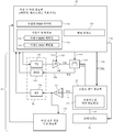
안테나 로딩 변동을 보상하기 위해 안테나(40)를 어떻게 조정할지를 결정하기 위해 안테나 성능 정보를 수집하고 처리하기 위한 예시적인 회로부가 도 6에 도시된다. 도 6에 도시된 바와 같이, 무선 통신 회로부(34)는 하나 이상의 안테나(40), 프론트 엔드 회로부(112), 무선 주파수 결합기 회로부(110), 전력 증폭기 회로부(108), 저잡음 증폭기 회로부(114), 송수신기 회로부(56), 및 수신 신호 강도 측정 회로부(122)를 포함할 수 있다.An exemplary circuit for collecting and processing antenna performance information to determine how to adjust the
저장 및 처리 회로부(28)는 베이스밴드 프로세서 회로부, 비휘발성 또는 휘발성 메모리와 같은 저장소, 및 무선 주파수 신호들을 전송 및/또는 수신하기 위해 무선 통신 회로부(34)를 제어하기 위한 제어 회로부를 포함할 수 있다. 디바이스(10)에 의해 전송될 디지털 데이터 신호들은 회로부(28) 내의 하나 이상의 베이스밴드 프로세서에 의해 생성될 수 있다. 회로부(28)는 디지털 데이터 신호들을 원하는 통신 프로토콜(예를 들어, 원하는 셀룰러 전화 표준 및 변조 방식, 무선 로컬 영역 네트워크 프로토콜 등)에 따라 변조할 수 있고, 송수신기 회로부(56)에(예를 들어, 송수신기 회로부(56) 내의 하나 이상의 송신기(102)에) 전송하기 위한 대응하는 출력 신호들을 제공할 수 있다. 송수신기 회로부(56)는 출력 신호들을 무선 주파수로 상향-변환하고 무선 주파수 신호들을 무선 주파수 전력 증폭기(PA) 회로부(108)에 전송하는 믹서 회로부를 포함할 수 있다. 원하는 경우, 송수신기 회로부(56)는 출력 신호들을 대응하는 아날로그 신호들로 변환하는 디지털-아날로그 변환기 회로부를 포함할 수 있다.The storage and
저장 및 처리 회로부(28) 내의 제어 회로부는 제어 경로(118)를 통해 전력 증폭기 회로부(108)에 제공되는 전압(Vcc)(예를 들어, 본 명세서에서 때때로 전력 공급 전압(Vcc) 또는 전력 증폭기 바이어스 전압(Vcc)으로 지칭됨)의 레벨을 조정할 수 있다. 바이어스 전압(Vcc)은 전력 증폭기 회로부(108) 내의 하나 이상의 능동 전력 증폭기 단계에 대한 전력 공급 전압으로서 사용될 수 있다. 데이터 전송 동안, 전력 증폭기 회로부(108)는 전송 신호들(TX)의 출력 전력을, 충분한 신호 전송을 보장하기에 충분히 높은 레벨로 증폭할 수 있다.The control circuitry within the storage and
전력 증폭기 회로부(108)의 출력은 무선 주파수 결합기(110)를 통해 무선 주파수 프론트 엔드 회로부(112)에 결합될 수 있다. 프론트 엔드 회로부(112)는 조정가능한 매칭 네트워크(111)와 같은 조정가능한 임피던스 매칭 회로부를 포함할 수 있다. 조정가능한 임피던스 매칭 회로부(111)는 안테나(40)가 회로부(34)의 나머지 부분에 임피던스 매칭되도록 보장하기 위해 조정되는, 저항기, 인덕터, 및 커패시터와 같은, 수동 및/또는 능동 (조정가능한) 컴포넌트들의 네트워크들을 포함할 수 있다. 저장 및 처리 회로부(28)는 제어 신호들(CTRL)을 제어 경로(116)를 통해 프론트 엔드(112) 내의 조정가능한 매칭 회로부(111)에 제공할 수 있다.The output of
일부 시나리오들에서, 처리 회로부(28)는 안테나(40)를 통해 전달될 신호들의 주파수에만 기초하여 선택되는 특정한 미리결정된 임피던스를 나타내기 위해 매칭 회로부(111)를 제어한다. 예를 들어, 처리 회로부(28)는 각각의 가능한 동작 주파수에 대응하는 매칭 회로부(111)에 대한 특정 설정을 식별하는, 매칭 회로부(111)에 대한 공장-교정(factory-calibrated) 데이터를 저장할 수 있다. 처리 회로부(28)가 무선 통신을 위해 사용될 주파수를 결정하면, 매칭 회로부(111)는 공장-교정 데이터에 의해 식별된 대응하는 설정에 배치된다. 그러나, 사용될 주파수에만 기초하여 그러한 선험적 조정을 수행하는 것은 정상 동작 동안 발생하는 후방 하우징 벽(12R)을 통한 임의의 잠재적 안테나 로딩 변동을 고려하지 않는다. 처리 회로부(28)는 따라서 안테나(40)가 후방 하우징 벽(12R)을 통해 어떻게 로딩되고 있는지에 기초하여 실시간으로 매칭 회로부(111)의 동적 조정을 수행할 수 있다(예를 들어, 회로부(28)가, 안테나(40)의 로딩 조건들에 상관없이 실시간으로 무선 회로부(34)의 나머지 부분의 임피던스와 매칭되도록 안테나(40)의 임피던스를 변경하도록).In some scenarios, the
일례로서, 손목(90)(도 5)과 같은 외부 물체가 안테나(40)에 근접하게 들어오면, 안테나(40)는 안테나(40)의 임피던스가 더 이상 회로부(34)의 나머지 부분에 매칭되지 않도록 로딩될 수 있다. 저장 및 처리 회로부(28)는 조정가능한 임피던스 매칭 네트워크(111)의 임피던스를, 손목(90)에 의해 로딩된 안테나(40)와 매칭되도록 제어할 수 있다. 매칭 네트워크(111)가 안테나(40)에 매칭되면, 안테나 로딩의 변화의 결과로서의 잠재적 디튜닝은 완화될 수 있고 안테나 효율은 최대화될 수 있다. 다른 예로서, 안테나(40)는 디바이스(10)가 사용자의 손목(90)(도 5)에 대해 위치(94)에서 배향될 때 제1 양만큼 로딩될 수 있고, 디바이스(10)가 위치(96)에서 배향될 때 제2 양만큼 로딩될 수 있다. 제어 회로부(28)는 디바이스(10)가 위치(94)에 있을 때 안테나 로딩의 제1 양을 완화시키는 제1 설정에 매칭 회로부(111)를 배치할 수 있고, 디바이스(10)가 위치(96)에 있을 때 안테나 로딩의 제2 양을 완화시키는 제2 설정에 회로부(111)를 배치할 수 있다. 저장 및 처리 회로부(28)는 추가적으로 또는 대안적으로, 원하는 경우(예를 들어, 도 2의 튜닝가능한 컴포넌트들(62)을 조정하기 위해), 상이한 안테나 로딩 조건들을 보상하기 위해 경로(124)를 통해 안테나(40)에 제어 신호들을 제공할 수 있다.As an example, if an external object, such as the wrist 90 (FIG. 5), comes in proximity to the
원하는 경우, 프론트 회로부(112)는 무선 주파수 스위칭 회로부(예를 들어, 다중화 회로), 필터링 회로부(예를 들어, 듀플렉서 및 다이플렉서), 또는 임의의 다른 원하는 무선 주파수 프론트 엔드 회로부와 같은 다른 회로부를 포함할 수 있다. 원하는 경우, 프론트 엔드(112) 내의 필터링 회로부는 입력(수신) 및 출력(전송) 신호들을 그들의 주파수에 기초하여 라우팅하는 데 사용될 수 있다. 예를 들어, 프론트 엔드(112) 내의 필터링 회로부는 결합기(110)로부터 수신된 (업링크) 신호들(TX)을 안테나(40)에 전송할 수 있고, 안테나(40)에 의해 수신된 수신(다운링크) 신호들(RX)을 수신 경로(113) 상에 라우팅할 수 있다. 원하는 경우, 저잡음 증폭기(LNA) 회로부(114)는 수신 경로(113) 상에 개재될 수 있다. 저잡음 증폭기 회로부(114)는 경로(113) 상의 수신 신호들(RX)을 증폭시킬 수 있다. 증폭된 수신 신호들(RX)은 송수신기 회로부(56)에(예를 들어, 송수신기 회로부(56) 내의 하나 이상의 수신기 회로부(106)에) 라우팅될 수 있다. 송수신기 회로부(56)는 경로(113)를 통해 수신된 신호들을 (예를 들어, 믹서 회로부를 사용하여 신호들을 베이스밴드 주파수로 하향-변환한 후에) 저장 및 처리 회로부(18) 내의 베이스밴드 회로부에 제공할 수 있다.The
결합기(110)는 안테나(40)로 그리고 그로부터 흐르는 안테나 신호들을 탭핑하는 데 사용될 수 있다. 결합기(110)로부터의 탭핑된 안테나 신호들은 송수신기 회로부(56) 내의 수신기 또는 별도의 수신기를 사용하여 처리될 수 있다. 도 6에 도시된 바와 같이, 결합기(110)는 탭핑된 안테나 신호들(TX')을 피드백 경로(120)를 통해 피드백 수신기(104)에 제공할 수 있다. 저장 및 처리 회로부(28)는 제어 경로(119)를 사용하여 결합기(110)를 제어할 수 있다. 예를 들어, 저장 및 처리 회로부(28)는 결합기(110)로 하여금, 전력 증폭기(108)에 의해 전송되고 있는 신호들(TX)의 탭핑된 버전(때때로 포워드 신호들로 지칭됨)을 수신기(104)에 제공하도록, 또는 안테나(40)로부터 반사된 전송 신호들(TX)의 대응하는 탭핑된 버전(때때로 리버스 신호들로 지칭됨)을 수신기(104)에 제공하도록 지시할 수 있다.The
탭핑된 신호들은 하향-변환되고 저장 및 처리 회로부(28)에 제공될 수 있다. 저장 및 처리 회로부(28)는 탭핑된 신호들을 처리하여 안테나(40)의 임피던스의 위상 및 크기 측정치들과 같은 안테나 성능 메트릭 정보를 생성할 수 있다. 예를 들어, 안테나(40)에 대한 포워드 및 리버스 신호들을 처리함으로써, 저장 및 처리 회로부(28)는 안테나(40)의 임피던스의 위상 및 크기에 관한 정보를 실시간으로 수집할 수 있다. 위상 및 크기 측정치들은 안테나(40)의 복소 임피던스를 나타내는 산란 파라미터(소위 "S-파라미터") 값들과 같은 복소 임피던스 데이터를 포함할 수 있다. S-파라미터들의 측정치들은 예를 들어, 신호 전송 동안 안테나(40)로부터 결합기(110)를 향해 다시 반사되는 무선 주파수 신호들의 양을 나타내는 측정된 반사 계수 파라미터 값들(소위 S11 값들)을 포함할 수 있다.The tapped signals may be down-converted and provided to the storage and
안테나(40)의 임피던스의 위상 및 크기는 안테나(40)의 동작이 디바이스(10)의 동작 환경에 의해 영향을 받았는지 여부(예를 들어, 외부 물체의 존재가 안테나(40)의 로딩을 디튜닝 또는 변화시켰는지 여부)를 결정하는 데 사용될 수 있다. 예를 들어, 저장 및 처리 회로부(28)는 수집된 위상 및 크기 정보의 변동(예를 들어, 지나치게 높은 크기의 S11 측정치들 등)을 검출하여, 외부 물체의 존재에 의해 안테나(40)가 디튜닝/로딩되었을 때를 식별할 수 있다. 저장 및 처리 회로부(28)가 안테나(40)가 안테나(40)의 로딩으로 인해(예를 들어, 사용자가 스트랩(16)을 조정하는 것, 스트랩(16)을 변경하는 것, 손목(90)에 대한 디바이스(10)의 배향을 조정하는 것, 스트랩(16)이 젖는 것, 상이한 사용자가 디바이스(10)를 착용하는 것 등으로 인해) 디튜닝되었음을 검출하는 경우, 회로부(28)는 디튜닝을 보상하기 위해 임피던스 매칭 네트워크(111)를 조정하도록 경로(116)를 통해 제어 신호들(CTRL)을 발행할 수 있다. 임피던스 매칭 네트워크(111)가 조정된 후, 안테나(40)는 무선 통신 회로부(34)의 나머지 부분과 임피던스 매칭되고 안테나 효율은 최대화된다.The phase and magnitude of the impedance of the
원하는 경우, 수신 신호 강도 정보와 같은 다른 성능 메트릭 정보가 사용되어, 안테나 로딩의 변동에 응답하여 회로부(111)를 어떻게 조정할지를 결정할 수 있다. 무선 통신 회로부(34) 내의 수신 신호 강도 측정 회로부(122)는 저잡음 증폭기 회로부(114)로부터 신호들(RX)을 수신할 수 있다. 측정 회로부(122)는 신호들(RX)의 수신 신호 강도를 나타내는 정보를 수집할 수 있다. 예를 들어, 측정 회로부(122)는 수신 신호들(RX)로부터 수신 신호 강도 표시자(RSSI) 값들을 수집할 수 있다. 하나의 적합한 배열에서, 회로부(122)는 수신된 무선 주파수 신호를 RSSI 값들을 추출하기 위한 알려진 전압 레벨로 변환하는 다이오드 검출기 회로부를 포함할 수 있다. RSSI 값들은 저장 및 처리 회로부(28)에 전송될 수 있다. 측정 회로부(122)에 의해 수집된 RSSI 값들은 수집된 RSSI 데이터(126)로서 회로부(28) 상에 축적 및 저장될 수 있다. 수집된 RSSI 데이터(126)는 일례로서, 데이터베이스 파일과 같은 데이터 구조로 회로부(28) 상에 저장될 수 있다.If desired, other performance metric information, such as received signal strength information, may be used to determine how to adjust
저장 및 처리 회로부(28)는 시간 경과에 따라 디바이스(10)의 물리적 위치를 추적할 수 있다. 예를 들어, GPS 수신기 회로부(42)(도 2)는 시간 경과에 따라 디바이스(10)의 위치를 식별하기 위한 위성 내비게이션 신호들을 수신할 수 있다. 다른 예로서, 알려진 위치를 갖는 무선 기지국에 대한 디바이스(10)의 위치를 결정하기 위해 단거리 송수신기(36)가 사용될 수 있다. 무선 기지국에 대한 디바이스(10)의 위치는 디바이스(10)의 공간적 위치를 식별하기 위해 무선 기지국의 알려진 위치와 비교될 수 있다. 일반적으로, 임의의 원하는 방법들이 디바이스(10)의 위치를 식별하는 데 사용될 수 있다. 디바이스(10)의 위치는 위도, 경도, 및/또는 고도 좌표와 같은 공간적 좌표, 또는 임의의 다른 원하는 공간적 좌표를 사용하여 식별될 수 있다.The storage and
RSSI 데이터(126)를 축적 및 저장할 때, 저장 및 처리 회로부(28)는 또한 각각의 RSSI 측정이 이루어진 시간(본 명세서에서 때때로 획득 시간 또는 RSSI 획득 시간으로 지칭됨) 및/또는 각각의 RSSI 측정이 이루어진 시간에서의 디바이스(10)의 지리적 위치(본 명세서에서 때때로 획득 위치 또는 웨어러블 전자 디바이스 획득 위치로 지칭됨)를 식별할 수 있다. 예를 들어, 수집된 RSSI 데이터(126)는 회로부(122)에 의해 측정된 특정 RSSI 값, 그 RSSI 값이 측정된 대응하는 획득 시간, 및/또는 그 RSSI 값이 측정되었을 때의 디바이스(10)의 위치를 식별하는 대응하는 웨어러블 전자 디바이스 획득 위치를 각각 식별하는 엔트리들(예를 들어, 데이터 구조 또는 데이터베이스 내의 행들)을 포함할 수 있다. 이러한 방식으로, 수집된 RSSI 데이터(126)는 저장 및 처리 회로부(28) 상에 시간 및 공간의 함수로서(즉, 디바이스 위치) 저장될 수 있다.When accumulating and storing the
원하는 경우, 저장 및 처리 회로부(28)는 디바이스(10)의 하나 이상의 사용자의 습관에 관한 정보를 사용자 통계치들(128)로서 축적 및 저장할 수 있다. 사용자 통계치들(128)은 회로부(28) 상의 메모리에 저장된 하나 이상의 데이터 구조(예를 들어, RSSI 데이터(126)와 동일한 데이터 구조 또는 상이한 데이터 구조)로 유지될 수 있다. 사용자 통계치들(128)은 위치 데이터(예를 들어, 디바이스(10)가 하루 중 상이한 시간들에서 전형적으로 위치되는 곳을 식별하는 정보), 사용자가 전형적으로 디바이스(10)를 착용하는 방식에 관한 정보, 디바이스(10)가 사용자에 의해 착용될 때 스트랩(16)의 전형적인 구성에 관한 정보, 안테나(40) 또는 무선 회로부 내의 다른 컴포넌트들의 전형적인 성능에 관한 정보(예를 들어, 성능 메트릭 데이터), 또는 디바이스(10)의 사용자의 일상 또는 습관에 관한 임의의 다른 정보를 포함할 수 있다.If desired, the storage and
원하는 경우, 사용자 통계치들(128)은 시간 및/또는 공간의 함수로서 RSSI 데이터의 미리결정된 패턴들을 식별하는 정보를 포함할 수 있다. 예를 들어, 사용자 RSSI 패턴들(132)이 회로부(28) 상에 저장될 수 있다. 사용자 RSSI 패턴들(132)은 사용자에 의한 디바이스(10)의 전형적인 동작과 연관되는 시간 및/또는 공간의 함수로서의 RSSI 값들의 미리결정된 패턴들일 수 있다. 예를 들어, 사용자가 하루를 보내는 동안(예를 들어, 잠에서 깨어나고, 직장으로 운전하고, 직장에서 집으로 운전하고, 잠이 드는 등), 수집된 RSSI 값들은 사용자가 하루를 보내는 동안의 안테나(40)의 성능과 연관된 미리결정된 패턴들을 나타낼 수 있다. 사용자 RSSI 패턴들(132)은 예를 들어, 안테나 매칭 조정을 요구하는 비정상적인 이벤트들이 발생했을 때를 결정하기 위해 회로부(28)에 의해 사용되는 백그라운드 또는 베이스라인 측정치의 역할을 할 수 있다. RSSI 패턴들(132)은, 원하는 경우, 디바이스(10)의 제조 동안에(예를 들어, 공장-교정 패턴들 또는 설정들을 사용하여) 디바이스(10) 상에 로딩될 수 있다. 원하는 경우, 저장 및 처리 회로부(28)는 회로부(122)에 의해 수행된 실시간 RSSI 측정치들에 기초하여 사용자 RSSI 패턴들(132)을 지속적으로 업데이트(훈련)할 수 있다. 예를 들어, 회로부(28)는 그것이 사용자의 행동을 학습할 때 또는 시간 경과에 따른 사용자의 행동의 임의의 변화를 설명하기 위해, RSSI 패턴들(132)을 업데이트할 수 있다. 이러한 방식으로, RSSI 패턴들(132)은 대응하는 사용자에 의한 디바이스(10)의 전형적인 동작을 반영할 수 있다. 원하는 경우, 사용자 RSSI 패턴들(132)은 다수의 사용자의 전형적인 행동과 연관된 패턴들을 포함할 수 있다.If desired,
원하는 경우, 사용자 통계치들(128)은 회로부(28) 상에 저장된 이벤트 RSSI 패턴들을 포함할 수 있다. 이벤트 RSSI 패턴들(134)은 디바이스(10)의 동작 또는 디바이스(10)의 사용자에 의해 수행된 행동들과 연관된 특정 이벤트들에 대응하는 시간 및/또는 공간의 함수로서의 RSSI 값들의 미리결정된 패턴들일 수 있다. 예를 들어, 주어진 이벤트 RSSI 패턴(134)은 사용자가 밴드(16)를 제거하는 것과 연관되는 것으로 예상되거나 미리결정되는 고정된 위치에서의 시간의 함수로서의 RSSI 값들의 시퀀스일 수 있다(예를 들어, 소위 밴드 교체 이벤트). 다른 예로서, 주어진 이벤트 RSSI 패턴은 사용자가 자신의 손목에서 디바이스(10)를 벗는 것과 연관되는 것으로 예상되거나 미리결정되는 고정된 위치에서의 시간의 함수로서의 RSSI 값들의 시퀀스일 수 있다. 또 다른 예로서, 주어진 이벤트 RSSI 패턴은 사용자가 스트랩(16)을 조이거나 느슨하게 하는 것과 연관되는 것으로 예상되거나 미리결정되는 시간 및 위치의 함수로서의 RSSI 값들의 시퀀스일 수 있다(예를 들어, 소위 스트랩 조정 이벤트). 또 다른 예로서, 주어진 이벤트 RSSI 패턴은 사용자의 손목(90)이 젖는 것과 연관되는 것으로 예상되거나 미리결정되는 시간의 함수로서의 RSSI 값들의 시퀀스일 수 있다.
이벤트 RSSI 패턴들(134)은, 원하는 경우, 디바이스(10)의 제조 동안(예를 들어, 교정 데이터) 디바이스(10) 상에 로딩될 수 있다. 원하는 경우, 저장 및 처리 회로부(28)는 회로부(122)에 의해 수행된 실시간 RSSI 측정치들에 기초하여 이벤트 RSSI 패턴들(134)을 지속적으로 업데이트(훈련)할 수 있다. 예를 들어, 회로부(28)는 다양한 이벤트 또는 행동이 수행되는 동안 안테나(40)가 어떻게 수행하는지를 학습함에 따라 RSSI 패턴들(134)을 업데이트할 수 있다. 각각의 RSSI 패턴(134)은 그것이 나타내는 이벤트의 유형을 식별하는 식별자 정보를 포함할 수 있다(예를 들어, 특정 RSSI 패턴(134)은 제1 사용자에 의해 수행된 스트랩 교체 이벤트에 대응하는 것으로서 라벨링될 수 있는 반면에, 다른 RSSI 패턴은 제2 사용자에 의해 수행된 스트랩 조정 이벤트에 대응하는 것으로서 라벨링될 수 있는 등). 이러한 방식으로, RSSI 패턴들(134)은 대응하는 사용자에 의한 디바이스(10)의 동작 동안에 발생할 수 있는 이벤트들을 반영할 수 있다. 원하는 경우, 사용자 RSSI 패턴들(132) 및/또는 이벤트 RSSI 패턴들(134)은 생략될 수 있다.
저장 및 처리 회로부(28)는 안테나(40)의 상이한 로딩 조건들을 보상하기 위해 매칭 회로부(111)를 언제 조정할지 그리고/또는 매칭 회로부(111)를 어떻게 조정할지를 결정할 때, 수집된 RSSI 데이터(126), 사용자 RSSI 패턴들(132), 이벤트 RSSI 패턴들(134), 다른 사용자 통계치들(128), 및/또는 다른 정보를 처리할 수 있다. 매칭 회로부(111)에 대한 매칭 설정들(130)은 저장 및 처리 회로부(28) 상에 저장될 수 있다. 매칭 설정들(130)은 통신 동작들 동안 사용될 매칭 회로부(111)에 대한 특정 임피던스 매칭 설정들을 식별할 수 있다. 매칭 설정들(130)은 회로부(28) 상의 하나 이상의 데이터 구조 상에 저장될 수 있다.The storage and
저장 및 처리 회로부(28)는 (예를 들어, 회로부(122)에 의해 수집된 RSSI 데이터(126), 사용자 RSSI 패턴들(132), 이벤트 RSSI 패턴들(134), 및/또는 다른 정보에 기초하여) 임의의 주어진 시간에 안테나(40)에 대한 특정 로딩 조건을 식별할 수 있다. 처리 회로부(28)는 식별된 로딩 조건에 대응하는 적절한 매칭 설정(130)을 검색할 수 있고, 그 설정을 구현하도록 매칭 회로부(111)를 제어할 수 있다. 예를 들어, 처리 회로부(28)는 안테나(40)가 건조한 손목(90)의 존재 상태에 있음을 처리 회로부(28)가 식별할 때 매칭 회로부(111)를 제1 설정(130)에 배치할 수 있는 반면, 처리 회로부(28)는 안테나(40)가 젖은 손목(90)의 존재 상태에 있음을 처리 회로부(28)가 식별할 때 매칭 회로부(111)를 제2 설정(130)에 배치한다.The storage and
매칭 설정들(130)은, 원하는 경우, 디바이스(10)의 제조 동안에(예를 들어, 공장-교정 설정들을 사용하여) 디바이스(10) 상에 로딩될 수 있다. 원하는 경우, 저장 및 처리 회로부(28)는 회로부(122)에 의해 수행된 실시간 RSSI 측정치들에 기초하여 매칭 설정들(130)을 지속적으로 업데이트하거나 덮어쓸 수 있다. 예를 들어, 회로부(28)는 다양한 로딩 조건 하에서 어떤 특정 설정들이 안테나(40)에 가장 잘 매칭되는지를 학습함에 따라 매칭 설정들(130)을 업데이트할 수 있다. 다른 적합한 배열에서, 회로부(28)는 만족스러운 매칭 설정이 발견될 때까지 가능한 상이한 매칭 설정들을 스위핑(sweep through)할 수 있다.
이러한 방식으로, 저장 및 처리 회로부(28)는 안테나 로딩의 변화에 대해 안테나(40)의 성능을 계속해서 모니터링할 수 있고, 실시간으로 그러한 변화를 보상하기 위해 매칭 회로부(111)를 능동적으로 조정할 수 있다. 따라서, 이러한 조정은 디바이스(10)를 동작시키는 상이한 사용자들, 사용자의 손목(90) 상의 디바이스(10)의 상이한 배향들, 상이한 스트랩 조임, 상이한 스트랩 재료들, 디바이스(10)에 상의 또는 그에 인접한 물 또는 습기의 존재, 또는 디바이스(10)의 정상 동작 동안 발생할 수 있는 안테나(40)의 로딩에 영향을 미치는 임의의 다른 환경 변동의 결과로서 발생하는 안테나 성능의 임의의 잠재적 악화를 동적으로 그리고 적응적으로 보상할 수 있다.In this manner, the storage and
도 6의 예는 단지 예시일 뿐이다. 원하는 경우, 저장 및 처리 회로부(28)는 매칭 회로부(111)를 어떻게 조정할지를 결정할 때, 수집된 RSSI 데이터를, 결합기(110)를 사용해 수집된 위상 및 크기 측정치들과 조합하여 사용할 수 있다. 결합기(110) 및 피드백 수신기 회로부(104)는, 위상 및 크기 측정치들이 매칭 회로부(111)를 조정하는 데 사용되지 않는 시나리오들에서 생략될 수 있다. 유사하게, 측정 회로부(122)는, RSSI 측정치들이 매칭 회로부(111)를 조정하는 데 사용되지 않는 시나리오들에서 생략될 수 있다. 원하는 경우, 안테나(40)는 신호들(TX)을 전송하고 수신 신호들(RX)을 측정 회로부(122)에 전달하는 단일 안테나를 포함할 수 있다. 다른 적합한 배열에서, 제1 안테나(40)가 결합기(110)로부터의 신호들(TX)을 전송하는 데 사용될 수 있는 반면에, 제2 안테나(40)는 RSSI 데이터를 수집하기 위한 신호들(RX)을 수신하는 데 사용된다. 일반적으로, 무선 통신 회로부(34)는 임의의 원하는 방식으로 배열된 임의의 원하는 회로부를 포함할 수 있다. 송수신기 회로부(56) 내의 회로부(102, 104, 106)는 각각 각자의 집적 회로들을 사용하여 구현될 수 있거나, 또는 하나 이상의 공유된 집적 회로 상에 함께 형성될 수 있다.The example of FIG. 6 is only an example. If desired, the storage and
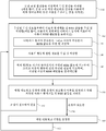
도 7은 매칭 회로부(111)를 조정하기 위한 RSSI 데이터를 수집 및 처리할 때 디바이스(10)에 의해 수행될 수 있는 예시적인 단계들의 흐름도이다. 도 7의 단계들은, 예를 들어, 실시간으로 안테나 로딩의 변동을 보상하기 위해(예를 들어, 디바이스(10)가 어떻게 착용되어 있는지, 누가 디바이스(10)를 착용하고 있는지 등에 상관없이 최적의 안테나 효율이 유지되도록) 디바이스(10)에 의해 수행될 수 있다.7 is a flow diagram of exemplary steps that may be performed by the
단계(140)에서, 무선 통신 회로부(34)는 공장 교정 설정들을 사용하여 무선 통신을 시작할 수 있다. 예를 들어, 저장 및 처리 회로부(28)는 통신에 사용될 특정 주파수에 대응하는 공장 교정 매칭 설정(130)을 식별할 수 있다. 공장 교정 설정들은 디바이스(10)의 제조 동안 회로부(28) 상에 로딩될 수 있다. 공장 교정 설정들은 예를 들어, 모든 실세계 안테나 로딩 조건들 하에서의 안테나(40)에 대한 충분한 임피던스 매칭을 제공하지 않을 수 있다. 무선 통신 회로부(34)는 (예를 들어, 공장 교정 설정들을 사용하여) 외부 디바이스들(52)(도 2)과 같은 외부 디바이스들에 신호들(TX)을 전송할 수 있고 외부 디바이스들(52)로부터 신호들(RX)을 수신할 수 있다.In
단계(142)에서, 저장 및 처리 회로부(28)는 (예를 들어, 도 6의 수신 신호 강도 측정 회로부(122)에 의해 측정된 바와 같이) 외부 디바이스들(52)로부터 수신되는 무선 신호들로부터 RSSI 값들(126)을 수집할 수 있다. 저장 및 처리 회로부(28)는 RSSI 값들이 수집되는 동안 디바이스(10)의 위치를 추적할 수 있다. 디바이스(10)가 무선 통신을 수행할 때, 회로부(28)는 디바이스(10)의 위치의 함수로서 그리고/또는 시간의 함수로서 수신된 신호들로부터 RSSI 값들을 계속해서 수집 및 저장할 수 있다(단계(144)).In
디바이스(10)는 또한 전송 및 수신된 신호들에 기초하여 사용자 통계치들(128)을 수집할 수 있다. 예를 들어, 저장 및 처리 회로부(28)는 사용자 통계치들(128)로서 사용자의 행동에 관한 정보를 저장할 수 있다(단계(146)). 행동 정보는 사용자가 하루 중 상이한 시간들에서 전형적으로 어디에 위치하는지에 대한 정보, 사용자에 의해 전형적으로 수행되는 활동들, 또는 사용자 행동과 연관된 다른 정보를 포함할 수 있다. 원하는 경우, 입출력 디바이스(32)(도 2) 내의 하나 이상의 센서는 사용자의 행동을 추적하는 것을 돕는 데 사용될 수 있다. 예를 들어, 디바이스(10) 상의 주변 광 센서 및/또는 모션 센서는, 사용자가 전형적으로 정지 상태, 잠든 상태, 움직이는 상태 등일 때의 시간들 또는 디바이스 위치들을 식별하는 데 사용될 수 있다. 다른 예로서, 스트랩 센서, 근접 센서, 터치 센서, 또는 다른 센서들은 사용자가 스트랩(16)을 제거하거나 조정할 때를 식별하는 데 사용될 수 있다.The
원하는 경우, 저장 및 처리 회로부(28)는 수집된 RSSI 데이터 및 사용자 행동에 관한 수집된 정보에 기초하여 저장된 RSSI 패턴들(132, 134)을 업데이트할 수 있다(단계(148)). 저장 및 처리 회로부(28)는 하나 이상의 사용자에 의한 디바이스(10)의 전형적 사용과 연관되는 사용자 RSSI 패턴들(132)을 식별 및 저장할 수 있다. 저장 및 처리 회로부(28)는 안테나(40)의 로딩에 영향을 미칠 수 있는 다양한 이벤트 또는 활동과 연관되는 이벤트 RSSI 패턴들(134)을 식별 및 저장할 수 있다. 예를 들어, 저장 및 처리 회로부(28)는 사용자가 스트랩(16)을 제거하거나 조정할 때 전형적으로 발생하는 수집된 RSSI 데이터 내의 패턴을 식별하기 위해, 사용자 통계치들(128)을 수집된 RSSI 데이터(126)와 비교할 수 있다. 식별된 패턴은 이벤트 RSSI 패턴들(134) 중 주어진 하나로서 저장될 수 있다. 유사하게, 저장 및 처리 회로부(28)는 수집된 RSSI 데이터(126) 내에서, 사용자의 정상적 착용에 대해 전형적인 패턴들(예를 들어, 사용자의 팔의 정상적 모션 또는 안테나(40)를 반드시 디튜닝하지는 않는 다른 전형적인 사용자 활동들과 연관된 패턴들)을 식별할 수 있다. 이러한 식별된 패턴들은 사용자 RSSI 패턴들(132)로서 저장될 수 있다. 디바이스(10)의 수명 전체에 걸쳐서, 저장 및 처리 회로부(28)는 디바이스(10)의 사용자의 행동 및 수집된 RSSI 데이터에 기초하여 사용자 RSSI 패턴들(132), 이벤트 RSSI 패턴들(134), 및/또는 다른 사용자 통계치들(128)을 계속해서 업데이트 및 정제(예를 들어, 훈련)할 수 있다. 도 7의 예는 단지 예시일 뿐이다. 원하는 경우, 단계들(144, 146, 및/또는 148)은 생략될 수 있다. 단계들(144, 146, 및/또는 148)은 동시에 또는 상이한 시간에 수행될 수 있다.If desired, the storage and
단계(150)에서, 저장 및 처리 회로부(28)는 매칭 회로부(111)에 대한 조정이 필요한지 여부를 결정하기 위해 수집된 사용자 통계치들(128) 및 수집된 RSSI 데이터(126)를 처리할 수 있다. 매칭 회로부에 대한 조정은, 안테나(40)의 로딩 조건들의 변화 또는 외부 물체들의 존재로 인한 안테나(40)의 디튜닝이 수집된 RSSI 데이터에서 검출될 때, 필요할 수 있다. 사용자 통계치들(128)은 예를 들어, 그러한 변화를 나타내는 수집된 RSSI 데이터(126) 내의 패턴들을 필터링 및/또는 식별하는 데 사용될 수 있다. 원하는 경우, 단계(150)는 단계(142)의 일부 또는 전부와 동시에 수행될 수 있다(예를 들어, 저장 및 처리 회로부(28)는 데이터 처리를 수행하면서도 계속해서 데이터를 수집 및 저장할 수 있다).At
처리 회로부(28)가 조정이 필요하지 않다고 결정하는 경우(예를 들어, 안테나 로딩 또는 안테나 디튜닝의 변화가 검출되지 않은 경우), 처리는 경로(152)에 의해 도시된 바와 같이 단계(142)로 되돌아가서 RSSI 데이터 및 사용자 통계치들을 계속해서 수집 및 저장할 수 있다. 처리 회로부(28)가 조정이 필요하다고 결정하는 경우(예를 들어, 안테나 로딩 또는 안테나 디튜닝의 변화가 검출되는 경우), 처리는 경로(154)에 의해 도시된 바와 같이 단계(160)로 진행할 수 있다.If the
단계(160)에서, 저장 및 처리 회로부(28)는 안테나 로딩/디튜닝의 검출된 변화를 보상하기 위해 매칭 회로부(111)를 조정할 수 있다. 예를 들어, 저장 및 처리 회로부(28)는 원하는 매칭 설정을 구현하기 위해 제어 회로부(111)에 경로(116)(도 6)를 통해 제어 신호들(CTRL)을 제공할 수 있다. 무선 통신 회로부(34)는 조정된 매칭 설정을 사용하여 무선 통신 동작들을 계속해서 수행할 수 있다. 처리는 후속적으로, 경로(162)에 의해 도시된 바와 같이 단계(142)로 되돌아가서 RSSI 데이터 및 사용자 통계치들을 계속해서 수집 및 저장할 수 있다.At
도 8은 매칭 회로부(111)에 대한 조정을 언제 수행할지를 결정하기 위해 저장 및 처리 회로부(28)에 의해 수행될 수 있는 예시적인 단계들의 흐름도이다. 예를 들어, 도 8의 단계들은 도 7의 단계(150)를 처리하는 동안 수행될 수 있다.Figure 8 is a flow diagram of exemplary steps that may be performed by the storage and
단계(170)에서, 처리 회로부(28)는 수집된 RSSI 데이터(126) 내에서, 시간 및/또는 디바이스 위치의 함수로서의 RSSI 값들의 시퀀스를 식별할 수 있다. 예를 들어, 처리 회로부(28)는 수집된 RSSI 데이터(126)로부터 가장 최근에 수집된 RSSI 값들의 세트를 식별할 수 있다.At
단계(172)에서, 처리 회로부(28)는 식별된 RSSI 값들에 대한 필터링 동작들을 수행할 수 있다. 예를 들어, 처리 회로부(28)는 시간의 함수로서의 식별된 RSSI 값들로부터 시간의 함수로서의 사용자 RSSI 패턴(132)을 필터링할 수 있다. 사용자 RSSI 패턴(132)은 제조 동안 디바이스(10) 상에 저장되는 공장 교정 패턴일 수 있고/있거나 정상 동작 동안 디바이스(10) 상에 저장 및 업데이트되는 패턴일 수 있다(예를 들어, 도 7의 단계(148)를 처리하는 동안). 이러한 방식으로, 처리 회로부(28)는, 그렇지 않으면 사용자에 의한 디바이스(10)의 정상 동작과 연관되는 베이스라인을 수집된 RSSI 데이터로부터 필터링할 수 있다. 다른 예로서, 처리 회로부(28)는 식별된 RSSI 값들로부터 일정한 베이스라인 RSSI 값을 필터링할 수 있다.At
단계(174)에서, 처리 회로부는 트리거 이벤트가 필터링된 RSSI 값들 내에 존재하는지 여부를 결정할 수 있다. 일례로서, 트리거 이벤트는 필터링된 RSSI 값들 내의 글리치(glitch)일 수 있다. 처리 회로부(28)는, 시간의 함수로서의 필터링된 RSSI 값들의 일부가 양의 기울기 임계치 값을 초과하는 기울기 또는 음의 기울기 임계치 값 미만인 기울기를 갖는 경우, 글리치가 존재한다고 결정할 수 있다. 다른 예로서, 트리거 이벤트는 필터링된 RSSI 값들 내의 과도한 편차일 수 있다. 처리 회로부(28)는 필터링된 RSSI 값들이 미리결정된 최소 임계 RSSI 값보다 작거나 미리결정된 최대 임계 RSSI 값보다 큰 값들을 포함하는 경우 과도한 편차가 존재한다고 결정할 수 있다. 또 다른 예로서, 처리 회로부(28)는 이벤트 RSSI 패턴들 중 하나가 필터링된 RSSI 값들 내에 존재하는지 여부를 결정하기 위해, 필터링된 RSSI 값들을 하나 이상의 미리결정된 이벤트 RSSI 패턴들(134)과 비교할 수 있다. 미리결정된 이벤트 RSSI 패턴들(134)은 제조 동안 디바이스(10) 상에 저장되는 공장 교정 패턴들일 수 있고/있거나 정상 동작 동안 디바이스(10) 상에 저장 및 업데이트되는 패턴들일 수 있다(예를 들어, 도 7의 단계(148)를 처리하는 동안). 처리 회로부(28)는, 필터링된 RSSI 값들의 특정 시퀀스가 사용자가 스트랩(16)을 제거하거나 조정하는 것과 연관된 RSSI 패턴과 같은 저장된 이벤트 RSSI 패턴(134)과 충분히 매칭될 때, 트리거 이벤트가 존재한다고 식별할 수 있다. 이 시나리오에서, 트리거 이벤트는 필터링된 데이터에서 검출된 이벤트 RSSI 패턴일 수 있다. 저장된 이벤트 RSSI 패턴들(134)은, 예로서, 상이한 사용자들이 디바이스(10)를 착용하는 것, 스트랩(16)을 조이거나 느슨하게 하는 것, 스트랩(16), 디바이스(10), 및/또는 손목(90) 상의 물 또는 습기의 존재 또는 부재, 손목(90) 상의 디바이스(10)의 위치 또는 배향의 변화 등에 대응하는 RSSI 값들의 시퀀스들을 포함할 수 있다.In
원하는 경우, 처리 회로부(28)는 필터링된 RSSI 값들, 사용자 통계치들(128), 및/또는 다른 정보의 조합에 기초하여 트리거 이벤트가 존재할 확률을 계산할 수 있다. 계산된 확률이 최소 확률 임계치를 초과하는 경우, 처리 회로부(28)는 트리거 이벤트가 존재한다고 결정할 수 있다. 계산된 확률이 최소 확률 임계치 이하인 경우, 처리 회로부(28)는 트리거 이벤트가 검출되지 않는다고 결정할 수 있다. 예로서, 처리 회로부(28)는 필터링된 RSSI 값들에서의 비교적 큰 저하(예를 들어, 미리결정된 최소 임계 RSSI 값 미만인 시간의 함수로서의 RSSI 값들의 과도한 편차)를 식별할 수 있다. 처리 회로부(28)는 이 정보를, 필터링된 RSSI 값들이 디바이스가 사용자의 직장 위치에 위치했던 오후 동안에 수집되었음을 식별하는 정보와 조합하여, 사용자가 스트랩(16)을 변경하는 것과 연관된 스트랩 변경 트리거 이벤트와 같은 트리거 이벤트가 수집된 RSSI 값들 내에 존재할 확률이 비교적 높다고 결정할 수 있다.If desired, processing
트리거 이벤트가 필터링된 RSSI 값들에서 검출되지 않는 경우(예를 들어, 글리치, 과도한 편차, 또는 미리결정된 RSSI 패턴이 존재하지 않는 경우), 처리는 경로(176)에 의해 도시된 바와 같이 단계(170)로 되돌아갈 수 있다. 처리 회로부(28)는 이어서, (예를 들어, 업데이트된 RSSI 값들 및 사용자 통계치들이 디바이스 동작 동안에 수집됨에 따라) 시간 및/또는 디바이스 위치의 함수로서의 후속적으로 수집된 RSSI 값들에서 트리거 이벤트들의 존재를 계속해서 검색할 수 있다. 트리거 이벤트가 검출되는 경우, 처리는 경로(178)에 의해 도시된 바와 같이 선택적 단계(180)로 진행할 수 있다.If the trigger event is not detected in the filtered RSSI values (e.g., glitch, excessive deviation, or no predetermined RSSI pattern), processing proceeds to step 170 as illustrated by
선택적 단계(180)에서, 처리 회로부(28)는 필터링된 RSSI 값들에 기초하여 저장된 이벤트 RSSI 패턴들(134)을 업데이트할 수 있다. 예를 들어, 트리거 이벤트가 검출되었을 때 특정 사용자 행동 또는 환경 이벤트가 발생했음을 식별하기 위해 센서 데이터, 사용자 입력, 또는 다른 정보가 사용될 수 있다. 그 사용자 행동 또는 환경 이벤트와 연관된 시간 및/또는 디바이스 위치의 함수로서의 수집된 RSSI 데이터의 패턴(시퀀스)은 향후 처리를 위해 회로부(28) 상에 이벤트 RSSI 패턴(134)으로서 저장될 수 있다. 예를 들어, 그 패턴은 원하는 경우 향후의 유사한 트리거 이벤트들을 식별하는 데 사용될 수 있다. 처리는 후속적으로, 매칭 네트워크(111)를 조정하는 도 7의 단계(160)로 진행할 수 있다.In
도 9는 트리거 이벤트를 검출하는 것에 응답하여 매칭 네트워크(111)를 동적으로 조정하기 위해 처리 회로부(28)에 의해 수행될 수 있는 예시적인 단계들의 흐름도이다. 예를 들어, 도 9의 단계들은 도 7의 단계(160)를 처리하는 동안 수행될 수 있다.9 is a flow diagram of exemplary steps that may be performed by the
단계(190)에서, 처리 회로부(28)는 매칭 회로부(111)에 대한 조정을 수행할 수 있다. 예를 들어, 처리 회로부(28)는 회로부(111)의 임피던스를 조정하기 위해 회로부(111) 내의 하나 이상의 컴포넌트를 제어할 수 있다.At
단계(192)에서, 처리 회로부(28)는 (예를 들어, 매칭 회로부가 조정된 임피던스를 나타내는 동안) 조정된 매칭 회로부를 사용하여 추가의 RSSI 값들을 수집할 수 있다.At
단계(194)에서, 처리 회로부(28)는 수집된 추가의 RSSI 값들을 조정이 이루어지기 전에 수집된 RSSI 값들과 비교함으로써 안테나(40)의 성능이 향상되었는지 여부를 결정할 수 있다. 예를 들어, 처리 회로부(28)는 추가의 RSSI 값들이 조정 이전에 수집된 RSSI 값들보다 큰 경우 안테나 성능이 향상되었다고 결정할 수 있다. 안테나 성능이 향상되지 않은 경우(예를 들어, 단계(192)에서 수집된 추가의 RSSI 값들이 조정 이전에 수집된 RSSI 값들 이하인 경우), 처리는 경로(196)에 의해 도시된 바와 같이 단계(190)로 되돌아갈 수 있고 매칭 회로부는 추가로 조정될 수 있다. 다른 적합한 배열에서, 단계(190)에서 수행된 조정은 되돌려질 수 있고 처리는 도 7의 단계(142)로 진행할 수 있다. 안테나 성능이 향상된 경우, 처리는 경로(198)에 의해 도시된 바와 같이 선택적 단계(200)로 진행할 수 있다.In
수집된 RSSI 값들이 이전에-수집된 RSSI 값들과 비교되는 도 9의 예는 단지 예시일 뿐이다. 원하는 경우, 처리 회로부(28)는 단계(192)에서 수집된 추가의 RSSI 값들을 미리결정된 임계치 값과 비교할 수 있다. 미리결정된 임계치 값은 산업 표준, 설계 표준, 규제적 표준, 제조 표준, 또는 임의의 다른 수단에 의해 결정될 수 있다. 미리결정된 임계치 값은 예를 들어, 디바이스(10)와 외부 장비(52) 사이의 만족스러운 링크 품질이 유지될 수 있는 최소 RSSI 값일 수 있다. 추가의 RSSI 값들이 미리결정된 임계치 값보다 큰 경우, 처리는 경로(198)에 의해 도시된 바와 같이 선택적 단계(200)로 진행할 수 있다. 추가의 RSSI 값들이 미리결정된 임계치 값 이하인 경우, 처리는 경로(196)에 의해 도시된 바와 같이 단계(190)로 되돌아갈 수 있다.The example of FIG. 9 in which collected RSSI values are compared with previously-collected RSSI values is only an example. If desired, the
선택적 단계(200)에서, 처리 회로부(28)는 조정된 매칭 네트워크 설정을 매칭 설정들(130)(도 6) 내의 엔트리로서 저장할 수 있다. 처리 회로부(28)는 회로부(111)에 대한 향후 조정을 수행하기 위해 저장된 매칭 네트워크 설정을 사용할 수 있다. 예를 들어, 처리 회로부(28)는 매칭 회로 조정을 야기한 대응하는 트리거 이벤트가 향후 검출될 때마다 특정 매칭 네트워크 설정(130)을 사용할 수 있다. 처리는 후속적으로 단계(202)로 진행할 수 있다.In
단계(202)에서, 무선 통신 회로부(34)는 조정된 매칭 네트워크 설정을 사용하여 통신을 계속할 수 있다(예를 들어, 처리는 도 7의 단계(142)로 진행할 수 있다). 이러한 방식으로, 처리 회로부(28)는 안테나 성능을 향상시키거나 최적화시키는 설정이 발견될 때까지 RSSI 데이터를 계속해서 수집하면서 매칭 네트워크(111)에 대한 많은 가능한 설정들을 스위핑할 수 있다. 이 예는 단지 예시일 뿐이다. 다른 적합한 배열에서, 미리결정된 매칭 설정들(130)은 매칭 네트워크(111)를 조정할 때 사용될 수 있다.In
도 10은 트리거 이벤트를 검출하는 것에 응답하여 미리결정된 매칭 설정들(130)에 기초하여 매칭 네트워크(111)를 조정하기 위해 처리 회로부(28)에 의해 수행될 수 있는 예시적인 단계들의 흐름도이다. 예를 들어, 도 10의 단계들은 도 7의 단계(160)를 처리하는 동안 수행될 수 있다.Figure 10 is a flow diagram of exemplary steps that may be performed by the
각각의 트리거 이벤트는 그것으로 하여금 수집된 RSSI 데이터 내에 존재하게 한 환경/안테나 로딩 인자들에 대응하는 유형을 가질 수 있다. 단계(210)에서, 처리 회로부(28)는 시간 및/또는 디바이스 위치의 함수로서의 필터링된 RSSI 값들, 사용자 통계치들(128), 사용자 입력, 센서 데이터, 및/또는 이벤트 RSSI 패턴들(134)에 기초하여 검출된 트리거 이벤트의 유형을 식별할 수 있다. 트리거 이벤트들의 유형들은 사용자가 자신의 손목 상의 디바이스(10)의 위치 또는 배향을 조정하는 것, (예를 들어, 스트랩(16)을 조이거나 느슨하게 함으로써) 사용자가 자신의 손목과 안테나(40) 사이의 거리를 조정하는 것, 사용자가 스트랩(16)을 상이한 스트랩으로 교체하는 것, 상이한 사용자가 디바이스(10)를 착용하는 것, 스트랩(16), 디바이스(10), 또는 손목(90)이 젖거나 건조해지는 것, 셔츠 소매와 같은 사용자의 의류의 부분이 디바이스(10)와 손목(90) 사이에 배치되거나 그 사이로부터 제거될 때, 또는 안테나(40)의 로딩에 영향을 미칠 수 있는 임의의 다른 환경 인자들과 연관된 트리거 이벤트들을 포함할 수 있다.Each trigger event may have a type corresponding to the environment / antenna loading factors that caused it to be present in the collected RSSI data. At
일례로서, 처리 회로부(28)는, 필터링된 RSSI 값들이 스트랩(16)을 교체하는 것과 연관된 이벤트 RSSI 패턴(134)과 매칭되는 경우, 디바이스(10) 내의 스트랩 센서가 스트랩(16)이 교체되었음을 검출하는 경우, 또는 임의의 다른 원하는 정보에 기초하여, 스트랩 교체와 연관된 트리거 이벤트(예를 들어, 스트랩 교체 유형 트리거 이벤트 또는 스트랩 교체 트리거 이벤트)가 발생했다고 식별할 수 있다. 예를 들어, 처리 회로부(28)는, 필터링된 RSSI 값들에서의 비교적 큰 저하가 디바이스가 사용자의 직장 위치에 위치했던 오후 동안에 측정되는 경우, 스트랩 교체 트리거 이벤트로서 트리거 이벤트를 식별할 수 있다. 다른 예로서, 처리 회로부(28)는, 수집된 RSSI 데이터가 시간 경과에 따른 측정된 RSSI 값들에서의 급격한 증가를 포함하였고 그 증가가 사용자의 위치가 직장 위치로부터 집 위치로 변화된 이후의 저녁 동안에 발생했다고 식별하는 것에 응답하여, 사용자가 자신의 손목으로부터 디바이스(10)를 제거하는 것을 트리거 이벤트의 유형으로서 식별할 수 있다(예를 들어, 사용자 통계치들(128)은 이러한 조건들의 세트가 사용자가 자신의 손목으로부터 디바이스(10)를 제거하는 것과 연관될 높은 확률을 갖는다고 식별할 수 있다). 또 다른 예로서, 처리 회로부(28)는, 수집된 RSSI 값들이 비교적 짧은 시간 동안 감소했다고 식별하면서 또한 디바이스 위치가 그 시간 동안 변하지 않았다고 식별하는 것에 응답하여, 사용자가 스트랩(16)을 조이는 것을 트리거 이벤트의 유형으로서 식별할 수 있다. 이들 예는 단지 예시일 뿐이며, 일반적으로, 처리 회로부(23)는 트리거 이벤트의 유형을 식별할 때, 디바이스 위치 및/또는 시간의 함수로서의 수집된 RSSI 정보, 사용자 입력, 센서 데이터, 이벤트 패턴들(134), 및 다른 사용자 통계치들(128)의 임의의 원하는 조합을 처리할 수 있다.As an example, the
단계(212)에서, 처리 회로부(28)는 트리거 이벤트의 식별된 유형에 대응하는 특정 매칭 설정(130)을 획득할 수 있다(예를 들어, 트리거 이벤트가 사용자가 스트랩(16)을 변경하는 것과 연관되는 것으로 식별된다면 제1 매칭 설정, 트리거 이벤트가 사용자의 피부가 젖는 것과 연관되는 것으로 식별된다면 제2 매칭 설정, 트리거 이벤트가 상이한 사용자가 디바이스(10)를 착용하는 것과 연관되는 것으로 식별된다면 제3 매칭 설정, 트리거 이벤트가 디바이스(10)가 도 5의 배향(94)으로 위치설정되는 것과 연관되는 것으로 식별된다면 제4 매칭 설정, 디바이스(10)가 도 5의 배향(96)으로 위치설정된다면 제5 매칭 설정 등). 획득된 매칭 설정(130)은 트리거 이벤트의 대응하는 유형이 검출될 때마다 사용되도록 디바이스(10)의 제조 동안 디바이스(10) 상에 로딩될 수 있거나, 또는 획득된 매칭 설정은 도 7의 단계(148)를 처리하는 동안 처리 회로부(28) 상에 저장될 수 있다.At
단계(214)에서, 처리 회로부(28)는 획득된 매칭 설정(130)을 매칭 네트워크(111)에 적용할 수 있다(예를 들어, 회로부(28)는 획득된 매칭 설정과 연관된 임피던스를 나타내도록 매칭 네트워크(111)를 구성할 수 있다). 처리는 후속적으로 선택적 단계(216)로 진행할 수 있다.In
선택적 단계(216)에서, 처리 회로부(28)는 조정된 매칭 회로부가 획득된 매칭 네트워크 설정을 사용하여 구성되는 동안 추가의 RSSI 값들을 수집할 수 있다. 처리 회로부(28)는 수집된 추가의 RSSI 값들을 조정이 이루어지기 전에 수집된 RSSI 값들과 비교함으로써 안테나(40)의 성능이 향상되었는지 여부를 결정할 수 있다. 안테나 성능이 향상되지 않은 경우(예를 들어, 단계(216)에서 수집된 추가의 RSSI 값들이 조정 이전에 수집된 RSSI 값들 이하인 경우), 처리는 단계(220)로 진행할 수 있다.In
단계(220)에서, 처리 회로부(28)는 적절한 조치를 취할 수 있다. 예를 들어, 처리 회로부(28)는 만족스러운 설정이 발견될 때까지 추가의 매칭 네트워크 설정들을 스위핑하는 것을 시작하는 도 9의 단계(190)로 진행할 수 있다. 다른 예로서, 처리 회로부(28)는 이전 매칭 설정으로 되돌리기 위해 매칭 회로부(111)를 제어할 수 있고, 처리는 사용자 통계치들 및 RSSI 값들을 계속해서 수집 및 처리하는 도 7의 단계(142)로 진행할 수 있다. 안테나 성능이 향상된 경우(예를 들어, 단계(216)에서 수집된 추가의 RSSI 값들이 조정 이전에 수집된 RSSI 값들보다 큰 경우), 처리는 단계(222)로 진행할 수 있다. 선택적 단계(216)가 수행되지 않는 시나리오들에서, 처리는 단계(214)로부터 단계(224)로 바로 진행할 수 있다.In
수집된 RSSI 값들이 이전에-수집된 RSSI 값들과 비교되는 도 10의 예는 단지 예시일 뿐이다. 원하는 경우, 처리 회로부(28)는 단계(216)에서 수집된 추가의 RSSI 값들을 미리결정된 임계치 값과 비교할 수 있다. 추가의 RSSI 값들이 미리결정된 임계치 값보다 큰 경우, 처리는 경로(222)에 의해 도시된 바와 같이 단계(224)로 진행할 수 있다. 추가의 RSSI 값들이 미리결정된 임계치 값 이하인 경우, 처리는 경로(218)에 의해 도시된 바와 같이 단계(220)로 진행할 수 있다.The example of FIG. 10 where collected RSSI values are compared to previously-collected RSSI values is only an example. If desired, the
단계(224)에서, 무선 통신 회로부(34)는 조정된 매칭 네트워크 설정을 사용하여 통신을 계속할 수 있다(예를 들어, 처리는 도 7의 단계(142)로 진행할 수 있다). 이러한 방식으로, 처리 회로부(28)는 수집된 RSSI 데이터에 기초하여 미리결정된 매칭 설정들(130)을 선택 및 사용할 수 있다. 이는 처리 회로부(28)가 (예를 들어, 도 9에 도시된 바와 같이) 상이한 설정들을 스위핑하는 시나리오들에서보다 더 빠른 안테나 조정을 허용할 수 있지만, 변화하는 또는 예측불가능한 환경 조건들(예를 들어, 회로부(28) 상에 최적화된 매칭 설정들이 아직 있지 않을 수 있는 조건들)에 덜 적응가능할 수 있다.At
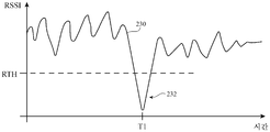
도 11은 수집된 RSSI 데이터(126)가 트리거 이벤트의 존재를 검출하기 위한 미리결정된 임계치와 어떻게 비교될 수 있는지를 보여주는 시간의 함수로서의 수집된 RSSI 값들의 예시적인 플롯이다. 도 11에 도시된 바와 같이, 곡선(230)은 (예를 들어, 도 7의 단계(144)를 처리하는 동안 수집된 바와 같이) 시간의 함수로서 그리고 고정된 위치에서 수집된 RSSI 값들을 나타낸다. 수집된 RSSI 값들(230)은 사용자가 디바이스(10)를 착용하는 동안 시간 경과에 따라 변할 수 있다. 값들(230)의 비교적 작은 변동은 안테나(40)의 전체 성능에 거의 영향을 미치지 않을 수 있다. 그러나, 비교적 큰 변동은 불만족스러운 안테나 성능을 초래할 수 있다.FIG. 11 is an exemplary plot of collected RSSI values as a function of time, showing how the collected
처리 회로부(28)는 트리거 이벤트를 식별하기 위해 RSSI 값들(230)을 처리할 수 있다(예를 들어, 도 8의 단계(174)를 처리하는 동안). 도 11의 예에서, 처리 회로부(28)는 RSSI 값들(230)을 미리결정된 임계치 값(RTH)과 비교할 수 있다. 처리 회로부(28)는 RSSI 값들(230)이 임계치 값(RTH) 미만으로 떨어지기 때문에 트리거 이벤트가 존재한다고 결정할 수 있다. 이 예는 단지 예시일 뿐이다. 원하는 경우, 처리 회로부(28)는 RSSI 값들(230)의 기울기를 식별할 수 있고 그 기울기를, 트리거 이벤트의 존재를 식별하기 위한 미리결정된 기울기 임계치와 비교할 수 있다. 다른 적합한 배열에서, 처리 회로부(28)는 RSSI 값들(230)이 미리결정된 이벤트 RSSI 패턴(134)과 매칭될 때 트리거 이벤트의 존재 및 유형을 식별할 수 있다. 설정된 위치에 대한 시간의 함수로서의 RSSI 값들이 처리되는 도 11의 예는 단지 예시일 뿐이다. 일반적으로, 처리 회로부(28)는 트리거 이벤트의 존재 및 유형을 식별하기 위해, 고정된 시간에서 위치의 함수로서 또는 위치 및 시간 둘 다의 함수(예를 들어, 수집된 RSSI 값들의 다차원 표면)로서 RSSI 값들을 처리할 수 있다.
도 12는 처리 회로부(28)가 트리거 이벤트의 존재를 식별하기 위해 미리결정된 사용자 및 이벤트 RSSI 패턴들을 사용하여 수집된 RSSI 값들을 어떻게 처리할 수 있는지를 보여주는 예시적인 도면이다.12 is an exemplary diagram showing how the
도 12에 도시된 바와 같이, 곡선(240)은 (예를 들어, 고정된 디바이스 위치에서) 시간의 함수로서 수집된 RSSI 값들을 도시한다. 곡선(242)은 특정 사용자 RSSI 패턴(132)(예를 들어, 도 7의 단계(148)를 처리하는 동안 축적된 시간의 함수로서의 RSSI 값들)을 도시한다. 사용자 RSSI 패턴(242)은 곡선(240)에 의해 나타내어진 동일한 위치 및 시간 값들의 함수로서의 전형적인 RSSI 데이터를 나타낼 수 있다. 사용자 RSSI 패턴(242)은 처리 회로부(28)가 사용자의 행동에 관한 정보를 계속해서 수집함에 따라(예를 들어, 사용자 통계치들(128)이 업데이트됨에 따라) 시간 경과에 따라 훈련 및 업데이트될 수 있다.As shown in FIG. 12,
사용자 RSSI 패턴(242)은 수집된 RSSI 값들(240)을 필터링하는 데 사용될 수 있다(예를 들어, 도 8의 단계(172)를 처리하는 동안). 도 12의 예에서, 사용자 RSSI 패턴(242)은 화살표(243)에 의해 도시된 바와 같이 수집된 RSSI 값들(240)로부터 필터링(감산)되어 필터링된 RSSI 값들(246)을 생성할 수 있다(예를 들어, 사용자 패턴(242)과 매칭되는 곡선(240)의 부분(244)은 필터링된 곡선(246)으로부터 제거될 수 있다). 이러한 방식으로, 사용자 RSSI 패턴(242)은 트리거 이벤트들을 식별하기 위해 수집된 RSSI 값들을 처리하기 위한 베이스라인 측정치로서 역할을 할 수 있다.The
처리 회로부(28)는 필터링된 RSSI 값들(246)을 처리하여 미리결정된 이벤트 RSSI 패턴이 필터링된 데이터 내에 존재하는지 여부를 결정할 수 있다(예를 들어, 도 8의 단계(174)를 처리하는 동안). 도 12의 예에서, 처리 회로부(28)는 필터링된 RSSI 값들(246)의 부분(250)이 주어진 이벤트 RSSI 패턴(248)과 매칭된다고 식별할 수 있다. 이벤트 RSSI 패턴(248)은 예를 들어, 도 8의 처리 단계(180) 동안, 도 7의 단계(148)를 처리하는 동안, 또는 공장 교정 동안 처리 회로부(28) 상에 저장될 수 있다. 일례로서, 이벤트 RSSI 패턴(248)은 스트랩 조임 트리거 이벤트와 연관된 RSSI 패턴일 수있다. 필터링된 RSSI 데이터(246) 내의 이벤트 RSSI 패턴(248)의 존재는 사용자가 스트랩(16)을 조이는 것을 나타낼 수 있다. 처리 회로부(28)는 후속적으로, 후속 통신 동안의(예를 들어, 적어도 다른 트리거 이벤트가 검출될 때까지) 사용을 위해, (예를 들어, 도 10의 단계(210)를 처리하는 동안) 스트랩 조임 트리거 이벤트에 대응하는 매칭 설정(130)을 식별할 수 있다. 다른 적합한 배열에서, 처리 회로부는 최적의 매칭 설정이 발견될 때까지 (예를 들어, 도 9의 단계들을 처리하는 동안) 상이한 매칭 네트워크 설정들을 스위핑할 수 있다. 매칭 네트워크 조정을 수행하는 것은 안테나(40) 주변의 환경이 안테나 로딩을 변화시킨 후에도(예를 들어, 안테나의 로딩이 스트랩(16)의 조임의 결과로서 변화한 후) 매칭 네트워크(111)가 안테나(40)와 매칭되도록 허용할 수 있다. 안테나(40)에 대한 적합한 매칭을 제공함으로써, 안테나 효율은 사용자가 디바이스(10)를 어떻게 착용하고 있는지에 상관없이 또는 누가 디바이스(10)를 착용하고 있는지에 상관없이 최대화될 수 있다.The
도 12의 예는 단지 예시일 뿐이다. 일반적으로, 수집된 RSSI 값들은 시간 및/또는 공간의 함수로서의 임의의 원하는 형상을 가질 수 있다. 유사하게, 사용자 RSSI 패턴(242) 및 이벤트 RSSI 패턴(248)은 임의의 원하는 형상을 가질 수 있다.The example of Fig. 12 is only an example. Generally, the collected RSSI values may have any desired shape as a function of time and / or space. Similarly, the
도 13은 매칭 회로부(111)를 조정하는 것이 특정 안테나 로딩 조건 하에서 안테나 성능에 어떻게 상이하게 영향을 미칠 수 있는지를 보여주는 스미스 차트이다. 도 13의 스미스 차트에서, 안테나(40)의 안테나 임피던스들은 상이한 동작 조건들의 함수로서 측정된다. 50 옴 안테나 임피던스는 도 13의 차트에서 임피던스 포인트(260)에 의해 특성화된다. 포인트(260)에 가까운 임피던스를 갖는 안테나는 디바이스(10) 내의 50 옴 전송 라인(예를 들어, 전송 라인(60))에 잘 매칭되는 것으로 여겨질 수 있다.13 is a Smith chart showing how adjusting the
안테나(40)는 디바이스(10)가 제1 안테나 로딩 조건 하에서 동작하는 동안(예를 들어, 디바이스(10)가 도 5의 위치(94)에 배향될 때) 제1 매칭 네트워크 설정으로 튜닝될 때 도 13의 영역(264) 내의 임피던스를 나타낼 수 있다. 영역(264)은 포인트(260)로부터 비교적 멀어서, 비교적 높은 레벨의 안테나 디튜닝을 나타낼 수 있다. 처리 회로부(28)는 결합기(110)(도 6)를 사용하여 위상 및 크기 정보를 수집함으로써 그리고/또는 수집된 RSSI 데이터에서 트리거 이벤트를 식별함으로써 이러한 디튜닝을 식별할 수 있다. 이러한 디튜닝을 보상하기 위하여, 제어 회로부(28)는 화살표(268)에 의해 도시된 바와 같이 안테나(40)를 제2 매칭 네트워크 설정으로 튜닝하도록 매칭 회로부(111)를 조정할 수 있다(예를 들어, 도 7의 단계(160)를 처리하는 동안). 제2 매칭 네트워크 설정으로 튜닝된 후, 안테나(40)는 영역(262) 내의 임피던스를 나타낼 수 있다. 영역(262)은, 영역(262)과 연관된 제2 매칭 네트워크 설정 하에서 동작될 때보다 더 낮은 레벨의 안테나 디튜닝을 나타내는 영역(264)보다 포인트(260)에 더 가깝다. 이러한 방식으로, 제어 회로부(28)는 사용자가 상이한 배향들로 디바이스(10)를 착용하는 것과 연관된 안테나 로딩의 가변량에 의해 야기된 안테나(40)의 디튜닝을 보상할 수 있다.
그러나, 안테나(40)는 디바이스(10)가 도 5의 위치(96)에서 배향될 때 상이한 임피던스를 나타낼 수 있다. 사용자가 디바이스(10)의 배향을 배향(94)으로부터 배향(96)으로 변화시키는 경우, 안테나(40)의 임피던스는 경로(266)에 의해 도시된 바와 같이 영역(264)과 같이 포인트(260)로부터 더 먼 영역으로 이동하여, 비교적 높은 레벨의 안테나 디튜닝을 나타낼 수 있다. 처리 회로부(28)는 후속적으로 이러한 디튜닝을 식별할 수 있고 매칭 회로부(111)를 제1 매칭 네트워크 설정으로 조정할 수 있다. 이는 안테나(40)의 디튜닝을 감소시키기 위해 안테나(40)의 임피던스를 포인트(260)에 더 가깝게 이동시킬 수 있다. 이러한 방식으로, 처리 회로부(28)는 정상 동작 동안 안테나(40)의 로딩 변동을 보상하기 위해 매칭 회로부(111)를 능동적으로 조정할 수 있다. 이 예는 단지 예시일 뿐이다. 일반적으로, 처리 회로부(28)는 임의의 적합한 이벤트(예를 들어, 사용자가 스트랩들을 변경하는 것, 사용자가 스트랩(16)을 조이는 것, 상이한 손목 생리를 갖는 상이한 사용자가 디바이스(10)를 착용하는 것, 물이 손목(90) 또는 디바이스(10)와 접촉하게 되는 것, 또는 안테나(40)의 동작 환경의 임의의 다른 변동)로 인한 안테나 로딩의 임의의 변화를 보상하기 위해 매칭 회로부(111)를 조정할 수 있다.However, the
도 14는 일 실시예에 따른 상이한 임피던스 매칭 회로 설정들 하에서 동작할 때 안테나에 의해 나타날 수 있는 예시적인 안테나 주파수 응답들의 그래프이다. 특히, 도 14는 동작 주파수의 함수로서 안테나 응답(전압 정재파 비(voltage standing wave ratio, VSWR))을 도시한다. 도 14에 도시된 바와 같이, 실선 곡선(270)은 제1 매칭 네트워크 설정 및 제1 안테나 로딩 조건 하에서 동작할 때 안테나(40)의 응답을 나타낸다. 예를 들어, 곡선(270)은 매칭 네트워크(111)가 제1 설정으로 설정되는 동안 제1 사용자가 디바이스(10)를 착용하는 것과 연관될 수 있다. 안테나(40)는 중간대역(MB) 및 고대역(HB) 주파수들에 대해서는 비교적 높은 응답을 갖지만 저대역(LB) 주파수들에서는 비교적 낮고 디튜닝된 응답을 가질 수 있다.14 is a graph of exemplary antenna frequency responses that may be exhibited by an antenna when operating under different impedance matching circuit configurations in accordance with one embodiment. In particular, Figure 14 shows the antenna response (voltage standing wave ratio, VSWR) as a function of the operating frequency. 14, the
점선 곡선(272)은 제1 매칭 네트워크 설정 및 제2 안테나 로딩 조건 하에서 동작할 때 안테나(40)의 응답을 나타낸다. 예를 들어, 곡선(272)은 매칭 네트워크(111)가 제1 설정으로 설정되는 동안 제2 사용자가 디바이스(10)를 착용하는 것과 연관될 수 있다. 이 시나리오에서, 안테나(40)는 (예를 들어, 안테나(40)를 상이하게 로딩하는 제1 사용자와 제2 사용자 사이의 상이한 생리로 인해) 저대역 주파수들에서 비교적 높은 응답을 가질 수 있다. 제1 사용자가 디바이스(10)를 착용하고 있을 때, 처리 회로부(28)는 저대역 주파수들에서 안테나(40)의 비교적 낮은 응답을 검출할 수 있다(예를 들어, 도 7의 단계(150)와 관련한 위상 및 크기 측정치들 및/또는 RSSI 값들을 사용하여). 처리 회로부(28)는 후속적으로 제1 사용자가 디바이스(10)를 착용하는 것으로 인한 안테나 로딩의 차이를 보상하는 제2 설정으로 매칭 네트워크(111)를 조정할 수 있다. 매칭 네트워크(111)를 제2 설정으로 조정한 후, 안테나(40)는 디바이스(10)가 제1 사용자에 의해 착용될 때 곡선(272)과 유사한 응답을 나타낼 수 있다. 제1 사용자가 디바이스(10)를 제2 사용자에게 착용하도록 준다면, 안테나(40)의 응답은 곡선(270)에 의해 도시된 응답으로 이동할 것이다. 처리 회로부(28)는 이 변화를 검출할 수 있고 후속적으로 매칭 네트워크(111)를 다시 제1 설정으로 조정할 수 있다. 네트워크(111)를 제1 설정으로 조정한 후, 안테나(40)는 곡선(272)에 의해 도시된 바와 같은 응답을 나타낼 수 있다. 이러한 방식으로, 처리 회로부(28)는 안테나 로딩 및 디튜닝의 변화를 실시간으로 보상하기 위해 회로부(111)를 능동적으로 조정할 수 있다.The dashed
도 14의 예는 단지 예시일 뿐이다. 일반적으로, 안테나(40)는 임의의 원하는 수의 상이한 주파수 대역들에서 동작할 수 있으며 동작 주파수의 함수로서 임의의 원하는 응답을 가질 수 있다. 안테나(40)는 환경 조건들에서의 임의의 변화의 결과로서 디튜닝될 수 있다. 도 1 내지 도 14의 예들이 손목시계 디바이스와 관련하여 기술되어 있지만, 임의의 원하는 전자 디바이스에 의해 유사한 동작들이 수행될 수 있다.The example of FIG. 14 is only an example. In general, the
디바이스(10)의 동작들(예를 들어, 도 7 내지 도 10의 동작들)은 제어 회로부(28)에 의해 수행될 수 있다. 동작 동안, 이 제어 회로부(때때로 처리 회로부, 처리 및 저장소, 컴퓨팅 장비, 컴퓨터 등으로 지칭될 수 있음)는 (예를 들어, 전용 하드웨어를 사용하여 그리고/또는 제어 회로부(28)와 같은 하드웨어 상에서 실행되는 소프트웨어 코드를 사용하여) 도 7 내지 도 10의 방법들 및/또는 다른 동작들을 수행하도록 구성될 수 있다. 이들 동작을 수행하기 위한 소프트웨어 코드는 비일시적(유형의) 컴퓨터 판독가능 저장 매체 상에 저장될 수 있다. 소프트웨어 코드는 때때로 소프트웨어, 데이터, 프로그램 명령어들, 명령어들, 또는 코드로 지칭될 수 있다. 비일시적 컴퓨터 판독가능 저장 매체는 비휘발성 랜덤 액세스 메모리(NVRAM)와 같은 비휘발성 메모리, 하나 이상의 하드 드라이브(예를 들어, 자기 드라이브 또는 솔리드 스테이트 드라이브), 하나 이상의 착탈식 플래시 드라이브 또는 다른 착탈식 매체, 다른 컴퓨터 판독가능 매체, 또는 이들 컴퓨터 판독가능 매체의 조합들을 포함할 수 있다. 비일시적 컴퓨터 판독가능 저장 매체 상에 저장된 소프트웨어는 제어 회로부(28)의 처리 회로부에 의해 실행될 수 있다. 처리 회로부는 처리 회로부를 갖는 주문형 집적 회로, 하나 이상의 마이크로프로세서, 또는 다른 처리 회로부를 포함할 수 있다.The operations of the device 10 (e.g., the operations of FIGS. 7 to 10) may be performed by the
일 실시예에 따르면, 웨어러블 전자 디바이스를 동작시키는 방법이 제공되며, 웨어러블 전자 디바이스는 전자 디바이스의 전면에 형성된 디스플레이, 전자 디바이스의 후면에 형성된 유전체 후방 하우징 벽, 안테나, 및 처리 회로부를 가지며, 이 방법은, 안테나가, 유전체 후방 하우징 벽을 통해 외부 장비로부터 무선 주파수 신호들을 수신하는 단계, 처리 회로부를 이용해, 유전체 후방 하우징 벽을 통한 외부 물체에 의한 안테나의 로딩의 양에 관한 정보를 수집하는 단계, 및 처리 회로부를 이용해, 유전체 후방 하우징 벽을 통한 외부 물체에 의한 안테나의 로딩의 양의 변화를 보상하기 위해 안테나를 조정하는 단계를 포함한다.According to one embodiment, there is provided a method of operating a wearable electronic device, the wearable electronic device having a display formed on a front surface of the electronic device, a dielectric rear housing wall formed on the back surface of the electronic device, an antenna, and processing circuitry, Includes the steps of the antenna receiving radio frequency signals from external equipment through the dielectric rear housing wall, using the processing circuitry to collect information about the amount of loading of the antenna by the external object through the dielectric rear housing wall, And using the processing circuitry to adjust the antenna to compensate for changes in the amount of loading of the antenna by an external object through the dielectric rear housing wall.
다른 실시예에 따르면, 안테나의 로딩의 양에 관한 정보를 수집하는 단계는 유전체 후방 하우징 벽을 통해 외부 장비로부터 수신된 무선 주파수 신호들에 기초한 수신 신호 강도 표시자(RSSI) 값들을 수집하는 단계를 포함하고, 유전체 후방 하우징 벽을 통한 외부 물체에 의한 안테나의 로딩의 양의 변화를 보상하기 위해 안테나를 조정하는 단계는 수집된 RSSI 값들에 기초하여 안테나를 조정하는 단계를 포함한다.According to another embodiment, collecting information regarding the amount of loading of the antenna includes collecting received signal strength indicator (RSSI) values based on radio frequency signals received from external equipment through the dielectric rear housing wall And adjusting the antenna to compensate for changes in the amount of loading of the antenna by the external object through the dielectric rear housing wall comprises adjusting the antenna based on the collected RSSI values.
다른 실시예에 따르면, 안테나의 로딩의 양에 관한 정보를 수집하는 단계는 수집된 RSSI 값들 각각과 연관된 획득 시간들을 저장하는 단계 및 수집된 RSSI 값들 각각과 연관된 웨어러블 전자 디바이스 획득 위치들을 저장하는 단계를 포함한다.According to another embodiment, collecting information regarding the amount of loading of the antenna includes storing acquisition times associated with each of the collected RSSI values, and storing wearable electronic device acquisition locations associated with each of the collected RSSI values .
다른 실시예에 따르면, 유전체 후방 하우징 벽을 통해 외부 물체에 의한 안테나의 로딩의 양의 변화를 보상하기 위해 안테나를 조정하는 단계는 수집된 RSSI 값들, 저장된 획득 시간들, 및 저장된 웨어러블 전자 디바이스 획득 위치들에 기초하여 안테나를 조정하는 단계를 포함한다.According to another embodiment, adjusting the antenna to compensate for a change in the amount of loading of the antenna by an external object through the dielectric rear housing wall may include gathering RSSI values, stored acquisition times, and a stored wearable electronic device acquisition location And adjusting the antenna based on the received signals.
다른 실시예에 따르면, 로딩의 양에 관한 정보를 수집하는 단계는 웨어러블 전자 디바이스 상의 무선 주파수 송신기 회로부에 의해 안테나에 전송되는 무선 주파수 신호들에 기초한 안테나의 임피던스의 위상 및 크기 측정치들을 수집하는 단계를 포함하고, 유전체 후방 하우징 벽을 통한 외부 물체에 의한 안테나의 로딩의 양의 변화를 보상하기 위해 안테나를 조정하는 단계는 안테나의 임피던스의 수집된 위상 및 크기 측정치들에 기초하여 안테나를 조정하는 단계를 포함한다.According to another embodiment, collecting information regarding the amount of loading includes collecting phase and magnitude measurements of the impedance of the antenna based on the radio frequency signals transmitted to the antenna by the radio frequency transmitter circuitry on the wearable electronic device And adjusting the antenna to compensate for a change in the amount of loading of the antenna by an external object through the dielectric rear housing wall comprises adjusting the antenna based on the collected phase and magnitude measurements of the impedance of the antenna .
다른 실시예에 따르면, 웨어러블 전자 디바이스는 무선 주파수 송수신기 회로부 및 무선 주파수 송수신기 회로부와 안테나 사이에 결합된 임피던스 매칭 회로부를 포함하고, 유전체 후방 하우징 벽을 통한 외부 물체에 의한 안테나의 로딩의 양의 변화를 보상하기 위해 안테나를 조정하는 단계는 임피던스 매칭 회로부의 임피던스를 조정하는 단계를 포함한다.According to another embodiment, the wearable electronic device includes a radio frequency transceiver circuitry and an impedance matching circuitry coupled between the radio frequency transceiver circuitry and the antenna, wherein the change in amount of loading of the antenna by an external object through the dielectric rear housing wall Adjusting the antenna to compensate includes adjusting the impedance of the impedance matching circuitry.
다른 실시예에 따르면, 안테나는 튜닝가능한 컴포넌트를 포함하고, 유전체 후방 하우징 벽을 통한 외부 물체에 의한 안테나의 로딩의 양의 변화를 보상하기 위해 안테나를 조정하는 단계는 튜닝가능한 컴포넌트를 조정하는 단계를 포함한다.According to another embodiment, the antenna includes a tunable component, and adjusting the antenna to compensate for a change in the amount of loading of the antenna by an external object through the dielectric rear housing wall comprises adjusting the tunable component .
일 실시예에 따르면, 대향하는 전면 및 후면을 갖는 웨어러블 전자 디바이스가 제공되며, 웨어러블 전자 디바이스는, 전자 디바이스의 후면을 형성하는 유전체 후방 하우징 벽, 전자 디바이스의 전면을 형성하는 디스플레이 커버 층을 갖는 디스플레이, 유전체 후방 하우징 벽과 중첩되는 전도성 트레이스들로 형성된 안테나 공진 요소 - 안테나 공진 요소는 유전체 후방 하우징 벽을 통한 외부 물체들에 의한 로딩을 받음 -, 안테나 공진 요소를 사용하여 유전체 후방 하우징 벽을 통해 무선 주파수 신호들을 전송 및 수신하도록 구성되는 무선 주파수 송수신기 회로부, 안테나 공진 요소와 무선 주파수 송수신기 회로부 사이에 결합된 임피던스 매칭 회로부, 및 유전체 후방 하우징 벽을 통한 안테나 공진 요소의 로딩의 변화를 검출하는 것에 응답하여 임피던스 매칭 회로부를 조정하도록 구성되는 저장 및 처리 회로부를 포함한다.According to one embodiment, there is provided a wearable electronic device having opposed front and back surfaces, the wearable electronic device comprising: a dielectric rear housing wall defining a back surface of the electronic device; a display having a display cover layer forming a front surface of the electronic device; An antenna resonant element formed of conductive traces overlapping the dielectric rear housing wall, the antenna resonant element being loaded by external objects through the dielectric rear housing wall, An impedance matching circuit coupled between the antenna resonant element and the radio frequency transceiver circuitry, and an antenna matching circuitry coupled to the dielectric resonant circuitry in response to detecting a change in loading of the antenna resonant element through the dielectric rear housing wall being A storage and processing circuitry is configured to adjust the residence matching circuit.
다른 실시예에 따르면, 웨어러블 전자 디바이스는 무선 주파수 송수신기 회로부와 임피던스 매칭 회로부 사이에 결합된 수신 경로 및 수신 경로에 결합된 수신 신호 강도 측정 회로부를 포함하며, 수신 신호 강도 측정 회로부는 수신 경로 상의 무선 주파수 신호들에 기초하여 수신 신호 강도 정보를 생성하도록 구성되고, 저장 및 처리 회로부는 생성된 수신 신호 강도 정보에 기초하여 안테나 공진 요소의 로딩의 변화를 검출하도록 구성된다.According to another embodiment, a wearable electronic device includes a receive path coupled between a receive path and a receive path coupled between a radio frequency transceiver circuit and an impedance matching circuit, And the storage and processing circuitry is configured to detect a change in loading of the antenna resonant element based on the generated received signal strength information.
다른 실시예에 따르면, 생성된 수신 신호 강도 정보는 수신 신호 강도 표시자(RSSI) 값들, RSSI 값들 각각과 연관된 획득 시간들, 및 RSSI 값들 각각과 연관된 웨어러블 전자 디바이스 획득 위치들을 포함한다.According to another embodiment, the generated received signal strength information includes received signal strength indicator (RSSI) values, acquisition times associated with each of the RSSI values, and wearable electronic device acquisition positions associated with each of the RSSI values.
다른 실시예에 따르면, 저장 및 처리 회로부는 RSSI 값들이 RSSI 값들의 미리결정된 패턴과 매칭되는지 여부를 결정함으로써 안테나 공진 요소의 로딩의 변화를 검출하도록 구성된다.According to another embodiment, the storage and processing circuitry is configured to detect a change in loading of the antenna resonant element by determining whether the RSSI values match a predetermined pattern of RSSI values.
다른 실시예에 따르면, 무선 주파수 송수신기 회로부는 안테나 공진 요소를 사용하여 유전체 후방 하우징 벽을 통해 700 ㎒ 내지 960 ㎒의 주파수들에서 신호들을 전송 및 수신하도록 구성되는 셀룰러 전화 송수신기를 포함한다.According to another embodiment, the radio frequency transceiver circuitry includes a cellular telephone transceiver configured to transmit and receive signals at frequencies between 700 MHz and 960 MHz through the dielectric rear housing wall using an antenna resonant element.
다른 실시예에 따르면, 웨어러블 전자 디바이스는 유전체 후방 하우징 벽으로부터 디스플레이 커버 층으로 연장되는 금속 하우징 측벽들, 전도성 트레이스들에 결합된 제1 안테나 피드 단자 - 전도성 트레이스들은 유전체 후방 하우징 벽 상에 패턴화됨 -, 금속 하우징 측벽들에 결합된 제2 안테나 피드 단자, 및 무선 주파수 송수신기 회로부를 제1 및 제2 안테나 피드 단자들에 결합하는 무선 주파수 전송 라인을 포함한다.According to another embodiment, the wearable electronic device comprises metal housing sidewalls extending from the dielectric rear housing wall to the display cover layer, a first antenna feed terminal coupled to the conductive traces, the conductive traces being patterned on the dielectric rear housing wall, A second antenna feed terminal coupled to the metal housing sidewalls, and a radio frequency transmission line coupling the radio frequency transceiver circuitry to the first and second antenna feed terminals.
다른 실시예에 따르면, 안테나 공진 요소는 사용자가 웨어러블 전자 디바이스를 착용하는 동안 사용자의 손목을 이용해 도파관을 형성하도록 구성된다.According to another embodiment, the antenna resonant element is configured to form a waveguide using the wearer's wrist while the user wears the wearable electronic device.
다른 실시예에 따르면, 웨어러블 전자 디바이스는 무선 주파수 송수신기 회로부에 결합된 전력 증폭기 회로부, 전력 증폭기 회로부와 임피던스 매칭 회로부 사이에 결합된 무선 주파수 결합기, 및 무선 주파수 결합기와 무선 주파수 송수신기 회로부 사이에 결합된 피드백 경로를 포함하며, 저장 및 처리 회로부는 피드백 경로를 통해 무선 주파수 결합기로부터 무선 주파수 송수신기 회로부에 의해 수신된 피드백 신호들에 기초하여 안테나 공진 요소의 임피던스의 위상 및 크기 측정치들을 수집하도록 구성되고, 저장 및 처리 회로부는 수집된 위상 및 크기 측정치들에 기초하여 안테나 공진 요소의 로딩의 변화를 검출하도록 추가로 구성된다.According to another embodiment, the wearable electronic device includes a power amplifier circuit portion coupled to the radio frequency transceiver circuitry, a radio frequency combiner coupled between the power amplifier circuitry and the impedance matching circuitry, and a feedback coupled between the radio frequency combiner and the radio frequency transceiver circuitry. Wherein the storage and processing circuitry is configured to collect phase and magnitude measurements of the impedance of the antenna resonant element based on the feedback signals received by the radio frequency transceiver circuitry from the radio frequency combiner through the feedback path, The processing circuitry is further configured to detect a change in loading of the antenna resonant element based on the collected phase and magnitude measurements.
일 실시예에 따르면, 웨어러블 전자 디바이스를 동작시키는 방법이 제공되며, 웨어러블 전자 디바이스는 전자 디바이스의 전면에 형성된 디스플레이, 전자 디바이스의 후면에 형성된 유전체 후방 하우징 벽, 안테나, 안테나에 결합된 임피던스 매칭 회로부, 및 처리 회로부를 가지며, 방법은, 안테나를 이용해, 유전체 후방 하우징 벽을 통해 외부 장비로부터 무선 주파수 신호들을 수신하는 단계, 처리 회로부를 이용해, 수신된 무선 주파수 신호들에 기초하여 수신 신호 강도 표시자(RSSI) 값들 및 대응하는 RSSI 획득 시간들을 수집 및 저장하는 단계, 처리 회로부를 이용해, 시간 경과에 따른 사용자에 의한 웨어러블 전자 디바이스의 동작과 연관된 사용자 통계치들을 축적하는 단계, 처리 회로부를 이용해, 트리거 이벤트를 검출하기 위해 축적된 사용자 통계치들, 저장된 RSSI 값들, 및 저장된 RSSI 획득 시간들을 처리하는 단계, 및 처리 회로부를 이용해, 트리거 이벤트를 검출하는 것에 응답하여, 임피던스 매칭 회로부를 조정하는 단계를 포함한다.According to one embodiment, a method of operating a wearable electronic device is provided, the wearable electronic device including a display formed on a front surface of the electronic device, a dielectric rear housing wall formed on a back surface of the electronic device, an antenna, impedance matching circuitry coupled to the antenna, And processing circuitry, the method comprising: receiving radio frequency signals from external equipment through the dielectric rear housing wall using an antenna; processing the received signal strength indicator (s) based on the received radio frequency signals using processing circuitry Collecting and storing RSSI values and corresponding RSSI acquisition times; accumulating user statistics associated with operation of the wearable electronic device by a user over time using processing circuitry; Users who have accumulated to detect Type teeth, the stored RSSI values, and processing the stored RSSI acquisition time, and using the processing circuitry, in response to detecting a trigger event, and a step of adjusting the impedance matching circuit portion.
다른 실시예에 따르면, 축적된 사용자 통계치들은 사용자 RSSI 패턴을 포함하고, 축적된 사용자 통계치들, 저장된 RSSI 값들, 및 저장된 RSSI 획득 시간들을 처리하는 단계는, 저장된 RSSI 값들로부터 사용자 RSSI 패턴을 필터링하여 필터링된 RSSI 값들을 생성하는 단계, 및 필터링된 RSSI 값들에 기초하여 트리거 이벤트를 검출하는 단계를 포함한다.According to another embodiment, the accumulated user statistics include a user RSSI pattern, and the processing of accumulated user statistics, stored RSSI values, and stored RSSI acquisition times may include filtering user RSSI patterns from stored RSSI values, Generating detected RSSI values, and detecting a trigger event based on the filtered RSSI values.
다른 실시예에 따르면, 사용자 통계치들은 유전체 후방 하우징 벽을 통한 안테나의 로딩의 변화와 연관된 이벤트 RSSI 패턴을 포함하고, 트리거 이벤트를 검출하는 단계는, 필터링된 RSSI 값들 내에서, 이벤트 RSSI 패턴과 매칭되는 RSSI 값들의 시퀀스를 검출하는 단계를 포함한다.According to another embodiment, the user statistics include an event RSSI pattern associated with a change in loading of the antenna through the dielectric rear housing wall, and the step of detecting the trigger event includes, within the filtered RSSI values, And detecting a sequence of RSSI values.
다른 실시예에 따르면, 임피던스 매칭 회로부를 조정하는 단계는, 조정된 임피던스를 나타내도록 임피던스 매칭 회로부를 제어하는 단계, 임피던스 매칭 회로부가 조정된 임피던스를 나타내는 동안 수신된 무선 주파수 신호들로부터 추가의 RSSI 값을 수집하는 단계, 수집된 추가의 RSSI 값에 기초하여 안테나의 무선 주파수 성능이 향상되었는지 여부를 결정하는 단계, 안테나의 무선 주파수 성능이 향상되지 않았다고 결정하는 것에 응답하여, 추가의 조정된 임피던스를 나타내도록 임피던스 매칭 회로부를 제어하는 단계, 및 안테나의 무선 주파수 성능이 향상되었다고 결정하는 것에 응답하여, 조정된 임피던스와 연관된 매칭 설정을 저장 회로부 상에 저장하는 단계를 포함한다.According to another embodiment, the step of adjusting the impedance matching circuitry further comprises the steps of controlling the impedance matching circuitry to indicate the adjusted impedance, adding additional RSSI values from the received radio frequency signals while the impedance matching circuitry indicates the adjusted impedance Determining if the radio frequency performance of the antenna has improved based on the collected additional RSSI value, in response to determining that the radio frequency performance of the antenna has not improved, indicating a further adjusted impedance And storing the matching configuration associated with the adjusted impedance on the storage circuitry in response to determining that the radio frequency performance of the antenna has been improved.
다른 실시예에 따르면, 임피던스 매칭 회로부를 조정하는 단계는, 웨어러블 전자 디바이스 상의 저장 회로부로부터 이벤트 RSSI 패턴과 연관된 매칭 설정을 검색하는 단계 - 매칭 설정은 조정된 임피던스를 식별함 -, 조정된 임피던스를 나타내도록 임피던스 매칭 회로부를 제어하는 단계, 임피던스 매칭 회로부가 조정된 임피던스를 나타내는 동안 수신된 무선 주파수 신호들로부터 추가의 RSSI 값을 수집하는 단계, 추가의 RSSI 값이 최소 RSSI 임계치 값을 초과하는지 여부를 결정하는 단계, 및 추가의 RSSI 값이 최소 RSSI 임계치 값을 초과하지 않는다고 결정하는 것에 응답하여, 추가의 조정된 임피던스를 나타내도록 임피던스 매칭 회로부를 제어하는 단계를 포함한다.According to another embodiment, adjusting the impedance matching circuitry comprises retrieving a matching setting associated with the event RSSI pattern from the storage circuitry on the wearable electronic device, wherein the matching setting identifies the adjusted impedance, , Collecting additional RSSI values from the received radio frequency signals while the impedance matching circuitry represents the adjusted impedance, determining whether the additional RSSI value exceeds the minimum RSSI threshold value And controlling the impedance matching circuitry to indicate a further adjusted impedance in response to determining that the additional RSSI value does not exceed the minimum RSSI threshold value.
상기 내용은 단지 예시일 뿐이며, 기술된 실시예들에 대해 다양한 수정들이 이루어질 수 있다. 전술한 실시예들은 개별적으로 또는 임의의 조합으로 구현될 수 있다.The above description is merely illustrative, and various modifications may be made to the embodiments described. The above-described embodiments may be implemented individually or in any combination.
Claims (20)
상기 안테나를 이용해, 상기 유전체 후방 하우징 벽을 통해 외부 장비로부터 무선 주파수 신호들을 수신하는 단계;
상기 처리 회로부를 이용해, 상기 유전체 후방 하우징 벽을 통한 외부 물체에 의한 상기 안테나의 로딩(loading)의 양에 관한 정보를 수집하는 단계; 및
상기 처리 회로부를 이용해, 상기 유전체 후방 하우징 벽을 통한 상기 외부 물체에 의한 상기 안테나의 상기 로딩의 양의 변화를 보상하기 위해 상기 안테나를 조정하는 단계를 포함하는, 방법.CLAIMS 1. A method of operating a wearable electronic device, the wearable electronic device having a display formed on a front surface of the electronic device, a dielectric rear housing wall formed on a back surface of the electronic device, an antenna, and processing circuitry,
Receiving radio frequency signals from external equipment through the dielectric rear housing wall using the antenna;
Using the processing circuitry to collect information about the amount of loading of the antenna by an external object through the dielectric rear housing wall; And
And using the processing circuitry to adjust the antenna to compensate for changes in the amount of loading of the antenna by the external object through the dielectric rear housing wall.
상기 전자 디바이스의 상기 후면을 형성하는 유전체 후방 하우징 벽;
상기 전자 디바이스의 상기 전면을 형성하는 디스플레이 커버 층을 갖는 디스플레이;
상기 유전체 후방 하우징 벽과 중첩되는 전도성 트레이스들로 형성된 안테나 공진 요소 - 상기 안테나 공진 요소는 상기 유전체 후방 하우징 벽을 통한 외부 물체들에 의한 로딩을 받음 -;
상기 안테나 공진 요소를 사용하여 상기 유전체 후방 하우징 벽을 통해 무선 주파수 신호들을 전송 및 수신하도록 구성되는 무선 주파수 송수신기 회로부;
상기 안테나 공진 요소와 상기 무선 주파수 송수신기 회로부 사이에 결합된 임피던스 매칭 회로부; 및
상기 유전체 후방 하우징 벽을 통한 상기 안테나 공진 요소의 상기 로딩의 변화를 검출하는 것에 응답하여 상기 임피던스 매칭 회로부를 조정하도록 구성되는 저장 및 처리 회로부를 포함하는, 웨어러블 전자 디바이스.1. A wearable electronic device having opposed front and rear surfaces,
A dielectric rear housing wall defining the rear surface of the electronic device;
A display having a display cover layer forming the front side of the electronic device;
An antenna resonant element formed of conductive traces overlapping the dielectric rear housing wall, the antenna resonant element being subject to loading by external objects through the dielectric rear housing wall;
A radio frequency transceiver circuitry configured to transmit and receive radio frequency signals through the dielectric rear housing wall using the antenna resonant element;
An impedance matching circuitry coupled between the antenna resonant element and the radio frequency transceiver circuitry; And
And storage and processing circuitry configured to adjust the impedance matching circuitry in response to detecting a change in the loading of the antenna resonant element through the dielectric rear housing wall.
상기 무선 주파수 송수신기 회로부와 상기 임피던스 매칭 회로부 사이에 결합된 수신 경로; 및
상기 수신 경로에 결합된 수신 신호 강도 측정 회로부를 추가로 포함하며, 상기 수신 신호 강도 측정 회로부는 상기 수신 경로 상의 무선 주파수 신호들에 기초하여 수신 신호 강도 정보를 생성하도록 구성되고, 상기 저장 및 처리 회로부는 상기 생성된 수신 신호 강도 정보에 기초하여 상기 안테나 공진 요소의 상기 로딩의 변화를 검출하도록 구성되는, 웨어러블 전자 디바이스.9. The method of claim 8,
A receive path coupled between the radio frequency transceiver circuitry and the impedance matching circuitry; And
Wherein the received signal strength measurement circuitry is further configured to generate received signal strength information based on the radio frequency signals on the receive path, Is configured to detect a change in the loading of the antenna resonant element based on the generated received signal strength information.
상기 안테나 공진 요소를 사용하여 상기 유전체 후방 하우징 벽을 통해 700 ㎒ 내지 960 ㎒의 주파수들에서 신호들을 전송 및 수신하도록 구성되는 셀룰러 전화 송수신기를 포함하는, 웨어러블 전자 디바이스.12. The apparatus of claim 11, wherein the radio frequency transceiver circuitry comprises:
And a cellular telephone transceiver configured to transmit and receive signals at frequencies between 700 MHz and 960 MHz through the dielectric rear housing wall using the antenna resonant element.
상기 유전체 후방 하우징 벽으로부터 상기 디스플레이 커버 층으로 연장되는 금속 하우징 측벽들;
전도성 트레이스들에 결합된 제1 안테나 피드(feed) 단자 - 상기 전도성 트레이스들은 상기 유전체 후방 하우징 벽 상에 패턴화됨 -;
상기 금속 하우징 측벽들에 결합된 제2 안테나 피드 단자; 및
상기 무선 주파수 송수신기 회로부를 상기 제1 및 제2 안테나 피드 단자들에 결합하는 무선 주파수 전송 라인을 추가로 포함하는, 웨어러블 전자 디바이스.12. The method of claim 11,
Metal housing sidewalls extending from the dielectric rear housing wall to the display cover layer;
A first antenna feed terminal coupled to the conductive traces, the conductive traces being patterned on the dielectric rear housing wall;
A second antenna feed terminal coupled to the metal housing sidewalls; And
And a radio frequency transmission line coupling the radio frequency transceiver circuitry to the first and second antenna feed terminals.
상기 무선 주파수 송수신기 회로부에 결합된 전력 증폭기 회로부;
상기 전력 증폭기 회로부와 상기 임피던스 매칭 회로부 사이에 결합된 무선 주파수 결합기; 및
상기 무선 주파수 결합기와 상기 무선 주파수 송수신기 회로부 사이에 결합된 피드백 경로를 추가로 포함하며, 상기 저장 및 처리 회로부는 상기 피드백 경로를 통해 상기 무선 주파수 결합기로부터 상기 무선 주파수 송수신기 회로부에 의해 수신된 피드백 신호들에 기초하여 상기 안테나 공진 요소의 임피던스의 위상 및 크기 측정치들을 수집하도록 구성되고, 상기 저장 및 처리 회로부는 상기 수집된 위상 및 크기 측정치들에 기초하여 상기 안테나 공진 요소의 상기 로딩의 변화를 검출하도록 추가로 구성되는, 웨어러블 전자 디바이스.9. The method of claim 8,
A power amplifier circuitry coupled to the radio frequency transceiver circuitry;
A radio frequency coupler coupled between the power amplifier circuitry and the impedance matching circuitry; And
Further comprising a feedback path coupled between the radio frequency combiner and the radio frequency transceiver circuitry, wherein the storage and processing circuitry receives feedback signals received by the radio frequency transceiver circuitry from the radio frequency combiner via the feedback path, Wherein the storage and processing circuitry is further configured to collect phase and magnitude measurements of the impedance of the antenna resonant element based on the acquired phase and magnitude measurements, ≪ / RTI >
상기 안테나를 이용해, 상기 유전체 후방 하우징 벽을 통해 외부 장비로부터 무선 주파수 신호들을 수신하는 단계;
상기 처리 회로부를 이용해, 상기 수신된 무선 주파수 신호들에 기초하여 수신 신호 강도 표시자(RSSI) 값들 및 대응하는 RSSI 획득 시간들을 수집 및 저장하는 단계;
상기 처리 회로부를 이용해, 시간 경과에 따른 사용자에 의한 상기 웨어러블 전자 디바이스의 동작과 연관된 사용자 통계치들을 축적하는 단계;
상기 처리 회로부를 이용해, 트리거 이벤트를 검출하기 위해 상기 축적된 사용자 통계치들, 상기 저장된 RSSI 값들, 및 상기 저장된 RSSI 획득 시간들을 처리하는 단계; 및
상기 처리 회로부를 이용해, 상기 트리거 이벤트를 검출하는 것에 응답하여, 상기 임피던스 매칭 회로부를 조정하는 단계를 포함하는, 방법.A method of operating a wearable electronic device, the wearable electronic device comprising: a display formed on a front surface of the electronic device; a dielectric rear housing wall formed on a back surface of the electronic device; an antenna; an impedance matching circuit portion coupled to the antenna; The method comprising:
Receiving radio frequency signals from external equipment through the dielectric rear housing wall using the antenna;
Using the processing circuitry to collect and store received signal strength indicator (RSSI) values and corresponding RSSI acquisition times based on the received radio frequency signals;
Accumulating user statistics associated with operation of the wearable electronic device by a user over time using the processing circuitry;
Using the processing circuitry to process the accumulated user statistics, the stored RSSI values, and the stored RSSI acquisition times to detect a trigger event; And
And using the processing circuitry to adjust the impedance matching circuitry in response to detecting the trigger event.
상기 저장된 RSSI 값들로부터 상기 사용자 RSSI 패턴을 필터링하여, 필터링된 RSSI 값들을 생성하는 단계; 및
상기 필터링된 RSSI 값들에 기초하여 상기 트리거 이벤트를 검출하는 단계를 포함하는, 방법.17. The method of claim 16, wherein the accumulated user statistics include a user RSSI pattern, and the processing the accumulated user statistics, the stored RSSI values, and the stored RSSI acquisition times comprises:
Filtering the user RSSI pattern from the stored RSSI values to generate filtered RSSI values; And
And detecting the trigger event based on the filtered RSSI values.
상기 필터링된 RSSI 값들 내에서, 상기 이벤트 RSSI 패턴과 매칭되는 RSSI 값들의 시퀀스를 검출하는 단계를 포함하는, 방법.18. The method of claim 17, wherein the user statistics include an event RSSI pattern associated with a change in loading of the antenna through the dielectric rear housing wall,
Detecting, within the filtered RSSI values, a sequence of RSSI values that match the event RSSI pattern.
조정된 임피던스를 나타내도록 상기 임피던스 매칭 회로부를 제어하는 단계;
상기 임피던스 매칭 회로부가 상기 조정된 임피던스를 나타내는 동안 상기 수신된 무선 주파수 신호들로부터 추가의 RSSI 값을 수집하는 단계;
상기 수집된 추가의 RSSI 값에 기초하여 상기 안테나의 무선 주파수 성능이 향상되었는지 여부를 결정하는 단계;
상기 안테나의 상기 무선 주파수 성능이 향상되지 않았다고 결정하는 것에 응답하여, 추가의 조정된 임피던스를 나타내도록 상기 임피던스 매칭 회로부를 제어하는 단계; 및
상기 안테나의 상기 무선 주파수 성능이 향상되었다고 결정하는 것에 응답하여, 상기 조정된 임피던스와 연관된 매칭 설정을 저장 회로부 상에 저장하는 단계를 포함하는, 방법.19. The method of claim 18, wherein adjusting the impedance matching circuitry comprises:
Controlling the impedance matching circuit section to indicate an adjusted impedance;
Collecting additional RSSI values from the received radio frequency signals while the impedance matching circuitry indicates the adjusted impedance;
Determining whether the radio frequency performance of the antenna is improved based on the collected additional RSSI value;
Responsive to determining that the radio frequency performance of the antenna has not improved, controlling the impedance matching circuitry to indicate a further adjusted impedance; And
Responsive to determining that the radio frequency performance of the antenna is improved, storing the matching setting associated with the adjusted impedance on the storage circuitry.
상기 웨어러블 전자 디바이스 상의 저장 회로부로부터 상기 이벤트 RSSI 패턴과 연관된 매칭 설정을 검색하는 단계 - 상기 매칭 설정은 조정된 임피던스를 식별함 -;
상기 조정된 임피던스를 나타내도록 상기 임피던스 매칭 회로부를 제어하는 단계;
상기 임피던스 매칭 회로부가 상기 조정된 임피던스를 나타내는 동안 상기 수신된 무선 주파수 신호들로부터 추가의 RSSI 값을 수집하는 단계;
상기 추가의 RSSI 값이 최소 RSSI 임계치 값을 초과하는지 여부를 결정하는 단계; 및
상기 추가의 RSSI 값이 상기 최소 RSSI 임계치 값을 초과하지 않는다고 결정하는 것에 응답하여, 추가의 조정된 임피던스를 나타내도록 상기 임피던스 매칭 회로부를 제어하는 단계를 포함하는, 방법.19. The method of claim 18, wherein adjusting the impedance matching circuitry comprises:
Retrieving from the storage circuitry on the wearable electronic device a matching setting associated with the event RSSI pattern, the matching setting identifying an adjusted impedance;
Controlling the impedance matching circuit portion to indicate the adjusted impedance;
Collecting additional RSSI values from the received radio frequency signals while the impedance matching circuitry indicates the adjusted impedance;
Determining whether the additional RSSI value exceeds a minimum RSSI threshold value; And
Responsive to determining that the additional RSSI value does not exceed the minimum RSSI threshold value, controlling the impedance matching circuitry to indicate a further adjusted impedance.
Applications Claiming Priority (2)
| Application Number | Priority Date | Filing Date | Title |
|---|---|---|---|
| US15/442,463 | 2017-02-24 | ||
| US15/442,463 US10484112B2 (en) | 2017-02-24 | 2017-02-24 | Dynamically adjustable antennas for wearable devices |
Publications (2)
| Publication Number | Publication Date |
|---|---|
| KR20180098140A true KR20180098140A (en) | 2018-09-03 |
| KR101949400B1 KR101949400B1 (en) | 2019-02-18 |
Family
ID=63112481
Family Applications (1)
| Application Number | Title | Priority Date | Filing Date |
|---|---|---|---|
| KR1020180018472A Active KR101949400B1 (en) | 2017-02-24 | 2018-02-14 | Dynamically adjustable antennas for wearable devices |
Country Status (5)
| Country | Link |
|---|---|
| US (1) | US10484112B2 (en) |
| JP (1) | JP6574005B2 (en) |
| KR (1) | KR101949400B1 (en) |
| CN (1) | CN108511879B (en) |
| DE (1) | DE102018202516A1 (en) |
Cited By (1)
| Publication number | Priority date | Publication date | Assignee | Title |
|---|---|---|---|---|
| WO2023106600A1 (en) * | 2021-12-09 | 2023-06-15 | 삼성전자 주식회사 | Antenna and wearable electronic device including same antenna |
Families Citing this family (17)
| Publication number | Priority date | Publication date | Assignee | Title |
|---|---|---|---|---|
| FR3055760B1 (en) * | 2016-09-02 | 2019-07-12 | Sigfox | ELECTRONIC APPARATUS COMPRISING AN ANTENNA STRUCTURE FOR TRANSMITTING AND / OR RECEIVING RADIO SIGNALS AND A STRING FOR ATTACHING THE APPARATUS |
| KR102414927B1 (en) * | 2018-03-21 | 2022-06-30 | 삼성전자 주식회사 | Method and apparatus for authenticating a device using wireless local area network service |
| CN109409450A (en) * | 2018-09-18 | 2019-03-01 | 四川西牛矩阵科技有限公司 | A kind of storehouse item location system based on RFID |
| US11523399B2 (en) * | 2018-09-25 | 2022-12-06 | New York University | System, method and computer-accessible medium for predicting wireless signal degradation |
| CN109561205B (en) * | 2018-11-01 | 2021-02-09 | 南京师范大学 | Smartphone-based space electromagnetic field recovery and display method |
| US10868356B1 (en) * | 2019-09-06 | 2020-12-15 | Apple Inc. | Electronic devices having extended antenna grounding rings |
| US10673514B1 (en) * | 2019-12-12 | 2020-06-02 | Motorola Mobility Llc | Communication device with receive antenna tuning |
| US11569858B2 (en) * | 2020-01-13 | 2023-01-31 | Apple Inc. | Adaptive antenna tuning system |
| TWI754944B (en) * | 2020-03-24 | 2022-02-11 | 日本商英幸技術股份有限公司 | Electromagnetic wave transceiving apparatus |
| CN111653863B (en) * | 2020-06-08 | 2022-04-19 | 安徽华米信息科技有限公司 | Wearable device and antenna adjusting method thereof |
| KR20220139041A (en) | 2021-04-07 | 2022-10-14 | 삼성전자주식회사 | A wearable electronic device comprising an antenna |
| CN113193337B (en) * | 2021-04-15 | 2022-11-25 | 安徽华米健康医疗有限公司 | Wearable device and wearing detection method thereof |
| US12181559B2 (en) * | 2021-05-26 | 2024-12-31 | Apple Inc. | Electronic devices with angular location detection capabilities |
| US12034493B2 (en) * | 2021-09-30 | 2024-07-09 | Arizona Board Of Regents On Behalf Of Arizona State University | Mismatch detection using periodic structures |
| CN114006182B (en) * | 2021-10-28 | 2025-08-26 | 歌尔科技有限公司 | Antenna adjustment system for smart wearable device and smart wearable device |
| WO2023140589A1 (en) * | 2022-01-21 | 2023-07-27 | 삼성전자주식회사 | Wearable electronic device comprising antenna |
| US12567885B2 (en) * | 2022-10-05 | 2026-03-03 | Boost SubscriberCo L.L.C. | Accessory device for satellite communications |
Citations (3)
| Publication number | Priority date | Publication date | Assignee | Title |
|---|---|---|---|---|
| CN201804995U (en) * | 2010-08-27 | 2011-04-20 | 佳邦科技股份有限公司 | Antenna structure integrated in ring housing |
| CN103943945A (en) * | 2014-02-21 | 2014-07-23 | 上海安费诺永亿通讯电子有限公司 | Watch antenna and watch with watch antenna |
| EP3040793A1 (en) * | 2014-12-29 | 2016-07-06 | LG Electronics Inc. | Watch-type mobile terminal and method of controlling the same |
Family Cites Families (20)
| Publication number | Priority date | Publication date | Assignee | Title |
|---|---|---|---|---|
| US5136719A (en) | 1988-12-05 | 1992-08-04 | Seiko Corp. | Automatic antenna tubing method and apparatus |
| JP2005249737A (en) * | 2004-03-08 | 2005-09-15 | Seiko Epson Corp | Clock with wireless communication function |
| US8781420B2 (en) | 2010-04-13 | 2014-07-15 | Apple Inc. | Adjustable wireless circuitry with antenna-based proximity detector |
| US9070969B2 (en) | 2010-07-06 | 2015-06-30 | Apple Inc. | Tunable antenna systems |
| US20120026009A1 (en) * | 2010-07-30 | 2012-02-02 | Yanzhu Zhao | Medical device having a multi-element antenna |
| US9153856B2 (en) | 2011-09-23 | 2015-10-06 | Apple Inc. | Embedded antenna structures |
| US20130328734A1 (en) * | 2012-06-06 | 2013-12-12 | Samsung Electronics Co., Ltd. | Adaptive antenna impedance matching |
| US9413409B2 (en) | 2013-03-15 | 2016-08-09 | Google Technology Holdings LLC | Method and apparatus for tuning an antenna based on unreliable data |
| CN103414488B (en) * | 2013-07-17 | 2016-05-25 | 小米科技有限责任公司 | A kind of control method, device and equipment of mobile device antenna |
| US9444425B2 (en) | 2014-06-20 | 2016-09-13 | Apple Inc. | Electronic device with adjustable wireless circuitry |
| US9537519B2 (en) | 2014-09-08 | 2017-01-03 | Apple Inc. | Systems and methods for performing power amplifier bias calibration |
| CN105490024B (en) * | 2014-09-23 | 2018-11-09 | 联想(北京)有限公司 | A kind of ACU antenna control unit, method and electronic equipment |
| CN104374490A (en) * | 2014-11-17 | 2015-02-25 | 王东方 | Passive wireless temperature monitoring lantern ring for metal bearing |
| CN105656526A (en) * | 2014-11-18 | 2016-06-08 | 深圳富泰宏精密工业有限公司 | Wearable device, system and method for selecting antenna |
| KR102245184B1 (en) | 2014-11-21 | 2021-04-27 | 삼성전자주식회사 | Electronic device with antenna |
| US9793599B2 (en) | 2015-03-06 | 2017-10-17 | Apple Inc. | Portable electronic device with antenna |
| US10461396B2 (en) | 2015-04-03 | 2019-10-29 | Fit Pay, Inc. | System and method for low-power close-proximity communications and energy transfer using a miniature multi-purpose antenna |
| US10461427B2 (en) | 2015-04-08 | 2019-10-29 | Samsung Electronics Co., Ltd. | Antenna and electronic devices comprising the same |
| CN106099362A (en) * | 2016-06-06 | 2016-11-09 | 珠海市魅族科技有限公司 | A kind of antenna switching method, antenna-switching device, antenna and router |
| CN106207459A (en) * | 2016-06-24 | 2016-12-07 | 联想(北京)有限公司 | A kind of wearable device |
-
2017
- 2017-02-24 US US15/442,463 patent/US10484112B2/en active Active
-
2018
- 2018-02-14 KR KR1020180018472A patent/KR101949400B1/en active Active
- 2018-02-20 DE DE102018202516.9A patent/DE102018202516A1/en active Pending
- 2018-02-23 JP JP2018030323A patent/JP6574005B2/en not_active Expired - Fee Related
- 2018-02-24 CN CN201810155956.7A patent/CN108511879B/en active Active
Patent Citations (3)
| Publication number | Priority date | Publication date | Assignee | Title |
|---|---|---|---|---|
| CN201804995U (en) * | 2010-08-27 | 2011-04-20 | 佳邦科技股份有限公司 | Antenna structure integrated in ring housing |
| CN103943945A (en) * | 2014-02-21 | 2014-07-23 | 上海安费诺永亿通讯电子有限公司 | Watch antenna and watch with watch antenna |
| EP3040793A1 (en) * | 2014-12-29 | 2016-07-06 | LG Electronics Inc. | Watch-type mobile terminal and method of controlling the same |
Cited By (1)
| Publication number | Priority date | Publication date | Assignee | Title |
|---|---|---|---|---|
| WO2023106600A1 (en) * | 2021-12-09 | 2023-06-15 | 삼성전자 주식회사 | Antenna and wearable electronic device including same antenna |
Also Published As
| Publication number | Publication date |
|---|---|
| US10484112B2 (en) | 2019-11-19 |
| CN108511879B (en) | 2021-02-02 |
| US20180248634A1 (en) | 2018-08-30 |
| KR101949400B1 (en) | 2019-02-18 |
| CN108511879A (en) | 2018-09-07 |
| JP2018142958A (en) | 2018-09-13 |
| DE102018202516A1 (en) | 2018-08-30 |
| JP6574005B2 (en) | 2019-09-11 |
Similar Documents
| Publication | Publication Date | Title |
|---|---|---|
| KR101949400B1 (en) | Dynamically adjustable antennas for wearable devices | |
| KR102216758B1 (en) | Electronic Devices Having Antenna Diversity Capabilities | |
| US10644383B2 (en) | Wristwatch antennas | |
| KR102193509B1 (en) | Wireless electronic device with radio-frequency sensors | |
| US9444425B2 (en) | Electronic device with adjustable wireless circuitry | |
| US10879606B2 (en) | Electronic device slot antennas | |
| CN107871932B (en) | Antenna with symmetrical switch architecture | |
| KR101916602B1 (en) | Broadband antenna | |
| KR101801503B1 (en) | Electronic device with slot antenna and proximity sensor | |
| KR101863013B1 (en) | Electronic device with fingerprint sensor and tunable hybrid antenna | |
| US9742459B2 (en) | Electronic device having sensors and antenna monitor for controlling wireless operation | |
| US8532697B2 (en) | Electronic device with passively combined antennas | |
| US10290941B2 (en) | Electronic device having multiband antenna with embedded filter | |
| TW201308753A (en) | Antenna switching system with adaptive switching criteria | |
| US20260088845A1 (en) | Adaptive Filtering for Sub-System Coexistence |
Legal Events
| Date | Code | Title | Description |
|---|---|---|---|
| E13-X000 | Pre-grant limitation requested |
St.27 status event code: A-2-3-E10-E13-lim-X000 |
|
| PA0109 | Patent application |
St.27 status event code: A-0-1-A10-A12-nap-PA0109 |
|
| A201 | Request for examination | ||
| PA0201 | Request for examination |
St.27 status event code: A-1-2-D10-D11-exm-PA0201 |
|
| R18-X000 | Changes to party contact information recorded |
St.27 status event code: A-3-3-R10-R18-oth-X000 |
|
| PG1501 | Laying open of application |
St.27 status event code: A-1-1-Q10-Q12-nap-PG1501 |
|
| E701 | Decision to grant or registration of patent right | ||
| PE0701 | Decision of registration |
St.27 status event code: A-1-2-D10-D22-exm-PE0701 |
|
| GRNT | Written decision to grant | ||
| PR0701 | Registration of establishment |
St.27 status event code: A-2-4-F10-F11-exm-PR0701 |
|
| PR1002 | Payment of registration fee |
St.27 status event code: A-2-2-U10-U11-oth-PR1002 Fee payment year number: 1 |
|
| PG1601 | Publication of registration |
St.27 status event code: A-4-4-Q10-Q13-nap-PG1601 |
|
| PR1001 | Payment of annual fee |
St.27 status event code: A-4-4-U10-U11-oth-PR1001 Fee payment year number: 4 |
|
| PR1001 | Payment of annual fee |
St.27 status event code: A-4-4-U10-U11-oth-PR1001 Fee payment year number: 5 |
|
| PR1001 | Payment of annual fee |
St.27 status event code: A-4-4-U10-U11-oth-PR1001 Fee payment year number: 6 |
|
| PR1001 | Payment of annual fee |
St.27 status event code: A-4-4-U10-U11-oth-PR1001 Fee payment year number: 7 |
|
| PR1001 | Payment of annual fee |
St.27 status event code: A-4-4-U10-U11-oth-PR1001 Fee payment year number: 8 |
|
| U11 | Full renewal or maintenance fee paid |
Free format text: ST27 STATUS EVENT CODE: A-4-4-U10-U11-OTH-PR1001 (AS PROVIDED BY THE NATIONAL OFFICE) Year of fee payment: 8 |