KR20180054686A - Apparatus and method for current sensor - Google Patents
Apparatus and method for current sensor Download PDFInfo
- Publication number
- KR20180054686A KR20180054686A KR1020187010297A KR20187010297A KR20180054686A KR 20180054686 A KR20180054686 A KR 20180054686A KR 1020187010297 A KR1020187010297 A KR 1020187010297A KR 20187010297 A KR20187010297 A KR 20187010297A KR 20180054686 A KR20180054686 A KR 20180054686A
- Authority
- KR
- South Korea
- Prior art keywords
- conductor
- magnetic field
- coil
- current
- current sensor
- Prior art date
Links
- 238000000034 method Methods 0.000 title claims description 38
- 239000004020 conductor Substances 0.000 claims abstract description 170
- 230000005540 biological transmission Effects 0.000 claims description 49
- 230000008878 coupling Effects 0.000 claims description 38
- 238000010168 coupling process Methods 0.000 claims description 38
- 238000005859 coupling reaction Methods 0.000 claims description 38
- 239000000758 substrate Substances 0.000 claims description 32
- 230000005684 electric field Effects 0.000 claims description 16
- 239000003990 capacitor Substances 0.000 claims description 14
- 238000001914 filtration Methods 0.000 claims description 9
- 230000001939 inductive effect Effects 0.000 claims description 5
- 230000004044 response Effects 0.000 claims description 4
- 238000005259 measurement Methods 0.000 description 10
- 238000013461 design Methods 0.000 description 7
- 238000012546 transfer Methods 0.000 description 7
- 238000010586 diagram Methods 0.000 description 6
- 230000000694 effects Effects 0.000 description 3
- 230000004907 flux Effects 0.000 description 3
- RYGMFSIKBFXOCR-UHFFFAOYSA-N Copper Chemical compound [Cu] RYGMFSIKBFXOCR-UHFFFAOYSA-N 0.000 description 2
- 229910052802 copper Inorganic materials 0.000 description 2
- 239000010949 copper Substances 0.000 description 2
- 230000009977 dual effect Effects 0.000 description 2
- 230000005672 electromagnetic field Effects 0.000 description 2
- 230000006870 function Effects 0.000 description 2
- 230000008569 process Effects 0.000 description 2
- 230000035945 sensitivity Effects 0.000 description 2
- 238000013459 approach Methods 0.000 description 1
- 239000000872 buffer Substances 0.000 description 1
- 230000001413 cellular effect Effects 0.000 description 1
- 230000008859 change Effects 0.000 description 1
- 238000004891 communication Methods 0.000 description 1
- 238000002847 impedance measurement Methods 0.000 description 1
- 230000006698 induction Effects 0.000 description 1
- 238000002955 isolation Methods 0.000 description 1
- 239000000463 material Substances 0.000 description 1
- 230000001902 propagating effect Effects 0.000 description 1
- 230000005855 radiation Effects 0.000 description 1
- 230000011664 signaling Effects 0.000 description 1
- 238000004804 winding Methods 0.000 description 1
- 229910000859 α-Fe Inorganic materials 0.000 description 1
Images


Classifications
-
- G—PHYSICS
- G01—MEASURING; TESTING
- G01R—MEASURING ELECTRIC VARIABLES; MEASURING MAGNETIC VARIABLES
- G01R15/00—Details of measuring arrangements of the types provided for in groups G01R17/00 - G01R29/00, G01R33/00 - G01R33/26 or G01R35/00
- G01R15/14—Adaptations providing voltage or current isolation, e.g. for high-voltage or high-current networks
- G01R15/20—Adaptations providing voltage or current isolation, e.g. for high-voltage or high-current networks using galvano-magnetic devices, e.g. Hall-effect devices, i.e. measuring a magnetic field via the interaction between a current and a magnetic field, e.g. magneto resistive or Hall effect devices
-
- G—PHYSICS
- G01—MEASURING; TESTING
- G01R—MEASURING ELECTRIC VARIABLES; MEASURING MAGNETIC VARIABLES
- G01R15/00—Details of measuring arrangements of the types provided for in groups G01R17/00 - G01R29/00, G01R33/00 - G01R33/26 or G01R35/00
- G01R15/14—Adaptations providing voltage or current isolation, e.g. for high-voltage or high-current networks
- G01R15/18—Adaptations providing voltage or current isolation, e.g. for high-voltage or high-current networks using inductive devices, e.g. transformers
- G01R15/181—Adaptations providing voltage or current isolation, e.g. for high-voltage or high-current networks using inductive devices, e.g. transformers using coils without a magnetic core, e.g. Rogowski coils
-
- G—PHYSICS
- G01—MEASURING; TESTING
- G01R—MEASURING ELECTRIC VARIABLES; MEASURING MAGNETIC VARIABLES
- G01R19/00—Arrangements for measuring currents or voltages or for indicating presence or sign thereof
- G01R19/0092—Arrangements for measuring currents or voltages or for indicating presence or sign thereof measuring current only
-
- H—ELECTRICITY
- H02—GENERATION; CONVERSION OR DISTRIBUTION OF ELECTRIC POWER
- H02J—CIRCUIT ARRANGEMENTS OR SYSTEMS FOR SUPPLYING OR DISTRIBUTING ELECTRIC POWER; SYSTEMS FOR STORING ELECTRIC ENERGY
- H02J50/00—Circuit arrangements or systems for wireless supply or distribution of electric power
- H02J50/10—Circuit arrangements or systems for wireless supply or distribution of electric power using inductive coupling
- H02J50/12—Circuit arrangements or systems for wireless supply or distribution of electric power using inductive coupling of the resonant type
-
- H02J7/025—
-
- H—ELECTRICITY
- H02—GENERATION; CONVERSION OR DISTRIBUTION OF ELECTRIC POWER
- H02J—CIRCUIT ARRANGEMENTS OR SYSTEMS FOR SUPPLYING OR DISTRIBUTING ELECTRIC POWER; SYSTEMS FOR STORING ELECTRIC ENERGY
- H02J7/00—Circuit arrangements for charging or depolarising batteries or for supplying loads from batteries
- H02J7/02—Circuit arrangements for charging or depolarising batteries or for supplying loads from batteries for charging batteries from ac mains by converters
- H02J7/04—Regulation of charging current or voltage
-
- H—ELECTRICITY
- H04—ELECTRIC COMMUNICATION TECHNIQUE
- H04B—TRANSMISSION
- H04B5/00—Near-field transmission systems, e.g. inductive loop type
- H04B5/0025—Near field system adaptations
- H04B5/0037—Near field system adaptations for power transfer
-
- H04B5/26—
-
- G—PHYSICS
- G01—MEASURING; TESTING
- G01R—MEASURING ELECTRIC VARIABLES; MEASURING MAGNETIC VARIABLES
- G01R33/00—Arrangements or instruments for measuring magnetic variables
- G01R33/007—Environmental aspects, e.g. temperature variations, radiation, stray fields
- G01R33/0076—Protection, e.g. with housings against stray fields
-
- H04B5/79—
Landscapes
- Engineering & Computer Science (AREA)
- Physics & Mathematics (AREA)
- General Physics & Mathematics (AREA)
- Power Engineering (AREA)
- Computer Networks & Wireless Communication (AREA)
- Environmental & Geological Engineering (AREA)
- Health & Medical Sciences (AREA)
- Toxicology (AREA)
- Condensed Matter Physics & Semiconductors (AREA)
- Measuring Instrument Details And Bridges, And Automatic Balancing Devices (AREA)
- Charge And Discharge Circuits For Batteries Or The Like (AREA)
- Arrangements For Transmission Of Measured Signals (AREA)
- Measurement Of Current Or Voltage (AREA)
- Signal Processing (AREA)
Abstract
전류 센서는 도체에 인접하게 배치된 감지 엘리먼트를 포함할 수도 있다. 전류 센서는 도체에 전류가 흐를 때 도체에서 발생된 제 1 자기장에 커플링하도록 구성될 수도 있다. 감지 엘리먼트에 전기적으로 접속된 출력부는 도체에서의 전류의 흐름을 나타내는 신호를 생성할 수 있다. 감지 엘리먼트는 도체에 전기적으로 접속된 부하에 의해 발생된 제 2 자기장의 자기력선과 평행한 평면에 배향될 수도 있다.The current sensor may include a sensing element disposed adjacent the conductor. The current sensor may be configured to couple to a first magnetic field generated in the conductor when a current flows through the conductor. An output electrically connected to the sensing element may produce a signal representative of the flow of current in the conductor. The sensing element may be oriented in a plane parallel to the lines of magnetic force of the second magnetic field generated by the load electrically connected to the conductor.
Description
본 개시는 일반적으로 전류 센서에 관한 것이다. 보다 구체적으로, 본 개시는 자기 유도를 이용한 전류 센서와 관련된 디바이스, 시스템 및 방법에 관한 것이다.This disclosure generally relates to current sensors. More particularly, this disclosure relates to devices, systems and methods associated with current sensors using magnetic induction.
무선 전력 전송은 이동 전화, 컴퓨터 태블릿 등과 같은 휴대용 전자 디바이스에서 인기가 높아지고 있는 기능인데, 왜냐하면 그러한 디바이스들은 일반적으로 긴 배터리 수명 및 낮은 배터리 중량을 필요로 하기 때문이다. 와이어를 사용하지 않고 전자 디바이스에 전력을 공급하는 능력은 휴대용 전자 디바이스의 사용자에게 편리한 솔루션을 제공한다. 예를 들어, 무선 전력 충전 시스템은 사용자가 물리적, 전기적 접속 없이 전자 디바이스들을 충전 및/또는 전력 공급하는 것을 허용할 수도 있으며, 이렇게 하여 전자 디바이스의 작동에 필요한 컴포넌트들의 수를 줄이고 전자 디바이스의 사용을 간편화한다.Wireless power transmission is an increasingly popular feature in portable electronic devices such as mobile phones, computer tablets, etc., because such devices typically require long battery life and low battery weight. The ability to power electronic devices without using wires provides a convenient solution for users of portable electronic devices. For example, a wireless power charging system may allow a user to charge and / or power electronic devices without physical and electrical connection, thereby reducing the number of components required for operation of the electronic device and reducing the use of the electronic device Simplify.
무선 전력 전송은 제조업자가 가전 디바이스에서 제한된 전원을 갖는 것에 기인하여 문제에 대한 창의적인 솔루션을 개발하는 것을 허용한다. 무선 전력 전송은 전력 어댑터 및 충전 코드와 같은 기존 충전 하드웨어를 제거할 수 있으므로 (사용자 및 제조업자 양자 모두에 대한) 전반적인 비용을 줄일 수도 있다. 산업 디자인 측면에서 무선 전력 송신기 및/또는 무선 전력 수신기를 구성하는 컴포넌트들 (예 : 자기 코일, 충전판 등) 에서의 상이한 크기와 모양을 갖는 것과 이동 핸드헬드 디바이스로부터 컴퓨터 랩톱까지 다양한 범위의 디바이스들에 대한 지원에 있어서 유연성이 있다.Wireless power transmission allows manufacturers to develop creative solutions to problems due to having a limited power supply in consumer electronics devices. Wireless power transmission can eliminate existing charging hardware such as power adapters and charging cords, thereby reducing overall costs (both for the user and the manufacturer). In terms of industrial design, a wide range of devices, from different handheld devices to computer laptops, having different sizes and shapes in components (e.g., magnetic coils, charging plates, etc.) that make up a wireless power transmitter and / There is flexibility in support for.
개요summary
본 발명의 일부 양태에서, 전류 센서는 도체에서의 전류의 흐름으로 인해 생길 수 있는 제 1 위치에서 발생된 제 1 자기장에 커플링하도록 구성된 감지 엘리먼트를 포함할 수도 있다. 전류 센서는 도체에서의 전류의 흐름을 나타내는 신호를 생성하기 위해 감지 엘리먼트에 전기적으로 접속된 출력부를 포함할 수도 있다. 감지 엘리먼트는 제 1 위치와는 상이한 제 2 위치에서 도체에 접속된 부하에 의해 발생된, 제 1 자기장과는 상이한, 제 2 자기장의 자기력선과 평행한 평면에 배향될 수도 있다.In some aspects of the invention, the current sensor may include a sensing element configured to couple to a first magnetic field generated at a first location that may occur due to current flow in the conductor. The current sensor may comprise an output electrically connected to the sensing element to produce a signal representative of the flow of current in the conductor. The sensing element may be oriented in a plane parallel to the lines of magnetic force of the second magnetic field, different from the first magnetic field, generated by a load connected to the conductors at a second location different from the first location.
일부 양태들에서, 감지 엘리먼트는 기판 상에 배치되고 도체에 인접하게 배치된 도전성 코일을 포함할 수도 있다. 전류 센서는 저항 (resistor) 및 캐패시터 (capacitor) 에 접속된 도전성 코일을 포함하는 필터 회로를 더 포함할 수도 있다. 일부 양태에서, 필터 회로는 대역통과 필터일 수도 있다. 일부 양태에서, 도전성 코일을 지니는 기판은 도체를 지니는 인쇄 회로 판 (PCB) 에 수직하게 배치될 수도 있다.In some aspects, the sensing element may comprise a conductive coil disposed on a substrate and disposed adjacent to the conductor. The current sensor may further comprise a filter circuit including a conductive coil connected to a resistor and a capacitor. In some aspects, the filter circuit may be a bandpass filter. In some embodiments, the substrate having the conductive coil may be disposed vertically on a printed circuit board (PCB) having conductors.
일부 양태에서, 부하는 무선 전력 전송을 위한 외부 자기장을 발생하도록 구성된 전력 송신 엘리먼트이다. 외부 자기장은 제 2 자기장을 구성한다. 일부 양태에서, 감지 엘리먼트는 도전성 코일을 포함할 수도 있다. 일부 양태에서, 전류 센서는 감지 엘리먼트의 도전성 코일을 포함하는 필터를 포함할 수도 있다. 필터는 전력 송신 엘리먼트의 공진 주파수에 동조될 수도 있다.In some aspects, the load is a power transmission element configured to generate an external magnetic field for wireless power transmission. The external magnetic field constitutes the second magnetic field. In some embodiments, the sensing element may comprise a conductive coil. In some embodiments, the current sensor may comprise a filter comprising a conductive coil of the sensing element. The filter may be tuned to the resonant frequency of the power transmitting element.
일부 양태에서, 전류 센서는 감지 엘리먼트에 인접하게 배치된 용량성 차폐부 (capacitive shield) 를 더 포함할 수도 있다. 용량성 차폐부는 도체 내의 전압에 의해 발생된 전기장이 감지 엘리먼트에 용량적으로 커플링되는 것을 방지할 수 있다. 일부 양태에서, 용량성 차폐부는 감지 엘리먼트와 도체 양자 모두에 인접하게 배치된 전도성 리드 (conductive lead) 일 수도 있다. 전도성 리드는 접지 전위에의 접속을 위해 구성된 자유 제 1 단부 및 제 2 단부를 가질 수도 있다.In some embodiments, the current sensor may further include a capacitive shield disposed adjacent to the sensing element. The capacitive shielding can prevent the electric field generated by the voltage in the conductor from being capacitively coupled to the sensing element. In some embodiments, the capacitive shield may be a conductive lead disposed adjacent to both the sensing element and the conductor. The conductive lid may have a free first end and a second end configured for connection to a ground potential.
일부 양태에서, 감지 엘리먼트는 제 1 평면 상에 배치된 제 1 도전성 코일 및 제 1 평면으로부터 이격된 적어도 제 2 평면 상에 배치된 적어도 제 2 도전성 코일을 포함할 수도 있다. 제 1 도전성 코일은 제 2 도전성 코일과 직렬로 접속될 수도 있다. 일부 양태에서, 제 1 도전성 코일은 다층 PCB 의 제 1 층 상에 형성된 트레이스일 수도 있고, 제 2 도전성 코일은 다층 PCB의 제 2 층 상에 형성된 트레이스일 수도 있다. 일부 양태에서, 제 1 도전성 코일은 도체의 일 측 상에 배치될 수도 있고, 제 2 도전성 코일은 도체의 다른 측 상에 배치될 수도 있다.In some embodiments, the sensing element may comprise a first conductive coil disposed on a first plane and at least a second conductive coil disposed on at least a second plane spaced from the first plane. The first conductive coil may be connected in series with the second conductive coil. In some embodiments, the first conductive coil may be a trace formed on a first layer of a multi-layer PCB, and the second conductive coil may be a trace formed on a second layer of a multi-layer PCB. In some embodiments, the first conductive coil may be disposed on one side of the conductor, and the second conductive coil may be disposed on the other side of the conductor.
일부 양태에서, 전류 센서는 제 1 도전성 코일 및 도체 양자 모두에 인접하게 배치되도록 구성된 제 1 용량성 차폐부 및 제 2 도전성 코일 및 도체 양자 모두에 인접하게 배치되도록 구성된 적어도 제 2 용량성 차폐부를 포함할 수도 있다.In some aspects, the current sensor includes a first capacitive shield configured to be disposed adjacent to both the first conductive coil and the conductor, and at least a second capacitive shield configured to be disposed adjacent to both the second conductive coil and the conductor You may.
일부 양태에서, 전류 센서는 제 1 도전성 코일 및 제 2 도전성 코일 중 어느 하나 또는 양자 모두를 포함하는 필터 회로를 포함할 수도 있다.In some aspects, the current sensor may include a filter circuit including either or both of the first conductive coil and the second conductive coil.
일부 양태에서, 감지 엘리먼트는 제 1 도전성 코일 및 적어도 제 2 도전성 코일을 포함할 수도 있으며, 제 1 및 제 2 코일들 양자 모두는 동일한 평면 상에 서로 이격되어 있다.In some embodiments, the sensing element may include a first conductive coil and at least a second conductive coil, wherein both the first and second coils are spaced apart from one another on the same plane.
본 개시에 따른 일부 양태에서, 도체에서 전류의 흐름을 감지하는 방법은 도체에서 전류의 흐름으로 인해서 도체로부터 생기는 제 1 자기장에 자기적 커플링함으로써 감지된 신호를 발생시키는 단계, 및 감지된 신호로부터 출력 신호를 발생시키는 단계를 포함할 수도 있다. 자기적 커플링은 도체에 전기적으로 접속된 부하를 통한 전류의 흐름에 의해 발생된 제 2 자기장의 역선 (field line) 과 평행한 평면에 일어날 수도 있다.In some aspects in accordance with the present disclosure, a method of sensing current flow in a conductor includes generating a sensed signal by magnetically coupling to a first magnetic field resulting from a conductor due to the flow of current in the conductor, And generating an output signal. The magnetic coupling may occur in a plane parallel to the field line of the second magnetic field generated by the flow of current through the load electrically connected to the conductor.
일부 양태에서, 제 1 자기장에 자기적 커플링하는 것은 도체에 인접하게 배치되고 제 2 자기장의 역선에 평행한 평면에 정렬된 도전성 재료의 코일에서, 제 1 자기장을 사용하여, 전류를 유도하는 단계를 포함할 수도 있다.In some embodiments, magnetically coupling to the first magnetic field comprises inducing a current in a coil of a conductive material disposed adjacent the conductor and aligned in a plane parallel to the opposite line of the second magnetic field, using a first magnetic field . ≪ / RTI >
일부 양태에서, 상기 방법은 도전성 재료의 코일을 포함하는 필터 회로에 의해 결정된 감지된 신호에서 주파수 성분들을 감쇠시키기 위해 감지된 신호를 필터링하는 단계를 더 포함할 수도 있다.In some aspects, the method may further comprise filtering the sensed signal to attenuate frequency components in a sensed signal determined by a filter circuit comprising a coil of conductive material.
일부 양태에서, 부하는 무선 전력 전송을 위한 외부 자기장을 발생시키도록 구성된 전력 송신 엘리먼트일 수도 있으며, 여기서 외부 자기장은 제 2 자기장을 구성한다.In some aspects, the load may be a power transmission element configured to generate an external magnetic field for wireless power transmission, wherein the external magnetic field constitutes a second magnetic field.
일부 양태에서, 상기 방법은 발생된 출력 신호가 실질적으로 상기 전기장으로부터의 영향이 없도록 도체에서 발생된 전기장으로부터 감지된 신호를 차폐하는 단계를 더 포함할 수도 있다.In some aspects, the method may further comprise shielding the sensed signal from an electric field generated in the conductor such that the generated output signal is substantially free of influence from the electric field.
일부 양태에서, 제 1 자기장에 자기적 커플링시키는 것은 제 1 자기장을 도체에 인접하게 배치된 도전성 재료의 제 1 코일에 커플링시키는 단계 및 제 1 자기장을 도체에 인접하게 배치된 도전성 재료의 제 2 코일에 커플링시키는 단계를 포함할 수도 있다.In some aspects, magnetically coupling to a first magnetic field comprises coupling a first magnetic field to a first coil of conductive material disposed adjacent the conductor, and coupling the first magnetic field to a conductive material adjacent the conductor 2 < / RTI > coil.
본 개시에 따른 일부 양태에서, 도체에서 전류의 흐름을 감지하기 위한 장치는 감지된 신호를 발생시키기 위하여 도체에서 전류의 흐름으로 인해서 도체로부터 생기는 제 1 자기장에 자기적 커플링하는 수단, 및 감지된 신호로부터 출력 신호를 발생시키는 수단을 포함할 수도 있다. 제 1 자기장에 자기적 커플링하는 수단은 도체에 전기적으로 접속된 부하를 통한 전류의 흐름에 의해 발생된 제 2 자기장의 역선과 평행한 평면에 정렬될 수도 있다.In some aspects in accordance with the present disclosure, an apparatus for sensing the flow of current in a conductor includes means for magnetically coupling to a first magnetic field resulting from a conductor due to the flow of current in the conductor to generate a sensed signal, And means for generating an output signal from the signal. The means for magnetically coupling to the first magnetic field may be arranged in a plane parallel to the reverse line of the second magnetic field generated by the flow of current through the load electrically connected to the conductor.
일부 양태들에서, 그 장치는 제 1 자기장에 자기적 커플링하는 수단을 포함하는 감지된 신호를 필터링하는 수단을 포함할 수도 있다. 제 1 자기장에 자기적 커플링하는 수단은 도전성 재료의 코일일 수도 있다. 그 필터링하는 수단은 대역통과 필터일 수도 있다.In some aspects, the apparatus may comprise means for filtering the sensed signal including means for magnetically coupling to the first magnetic field. The means for magnetically coupling to the first magnetic field may be a coil of a conductive material. The means for filtering may be a bandpass filter.
본 발명의 일부 양태에서, 수신기 디바이스에 충전 전력을 무선으로 송신하기 위한 장치는 송신 코일, 도체를 통해 송신 코일에 전기적으로 결합된 구동기 회로, 및 도체에서 전류의 흐름을 감지하도록 구성된 전류 센서를 포함할 수도 있다. 구동기 회로는 도체를 통해 교류로 송신 코일을 구동하도록 구성될 수도 있다. 전류 센서는 도체에서 전류의 흐름을 나타내는 신호를 생성하기 위해 도체에서 교류에 의해 발생된 제 1 자기장에 커플링하도록 구성된 감지 코일을 포함할 수도 있다. 송신 코일은 교류에 의해 구동되는 것에 응답하여 수신기 디바이스에 충전 전력을 무선으로 송신하기 위해 제 2 자기장을 발생시키도록 구성될 수도 있다. 감지 코일은 제 2 자기장의 역선에 평행한 평면에 배향될 수도 있다.In some aspects of the invention, an apparatus for wirelessly transmitting charging power to a receiver device includes a transmit coil, a driver circuit electrically coupled to the transmit coil through the conductor, and a current sensor configured to sense a current flow in the conductor You may. The driver circuit may be configured to drive the transmit coil in alternating current through a conductor. The current sensor may include a sense coil configured to couple to a first magnetic field generated by an alternating current in the conductor to produce a signal indicative of a current flow in the conductor. The transmit coil may be configured to generate a second magnetic field for wirelessly transmitting charge power to the receiver device in response to being driven by the alternating current. The sense coils may be oriented in a plane parallel to the opposite line of the second magnetic field.
일부 양태들에서, 장치는 감지 코일 및 감지 코일에 전기적으로 접속된 저항 및 커패시터를 포함하는 필터 회로를 포함할 수도 있다. 그 필터는 대역통과 필터일 수도 있다.In some aspects, the apparatus may comprise a filter circuit comprising a sense coil and a resistor and a capacitor electrically connected to the sense coil. The filter may be a bandpass filter.
일부 양태에서, 전류 센서는 감지 코일에 인접하게 배치된 용량성 차폐부를 포함할 수도 있다. 용량성 차폐부는 도체에서 생성된 전기장이 감지 코일에 용량적으로 커플링되는 것을 방지할 수 있으며, 용량성 차폐부는 도체와 감지 코일 사이에 배치된 제 2 도체를 포함한다.In some aspects, the current sensor may include a capacitive shield disposed adjacent the sense coil. The capacitive shield may prevent the electric field generated in the conductor from being capacitively coupled to the sense coil, and the capacitive shield includes a second conductor disposed between the conductor and the sense coil.
다음의 상세한 설명 및 첨부 도면들은 본 개시의 본질 및 이점들의 보다 나은 이해를 제공한다.The following detailed description and the annexed drawings provide a better understanding of the nature and advantages of the present disclosure.
이하의 논의 그리고 특히 도면을 참조하여, 도시된 세부 사항은 예시적인 논의의 목적을 위한 예를 보여주며, 본 개시의 원리 및 개념적인 양태들에 대한 설명을 제공하기 위해 제시된다는 점이 강조되야 한다. 이와 관련하여, 본 개시의 기본적인 이해를 위해 필요한 것을 넘어서 구현 상세들을 보여주려 시도되지 않는다. 도면과 관련하여 이하의 설명은 당업자에게 본 개시에 따른 실시형태들이 어떻게 실시될 수 있는지를 명백하게 한다. 첨부 도면들에서:
도 1 은 예시적 실시형태에 따른, 무선 전력 전송 시스템의 기능 블록도이다.
도 2 은 예시적 실시형태에 따른, 무선 전력 전송 시스템의 기능 블록도이다.
도 3 은 예시적인 실시형태에 따른, 전력 송신 또는 수신 엘리먼트를 포함하는 도 2의 송신 회로 또는 수신 회로의 일부의 개략도이다.
도 4a 및 도 4b는 본 개시에 따른 전류 센서를 구체화하는 예시적인 구성을 나타낸다.
도 5a, 도 5b 및 도 5c는 본 개시에 따른 전류 센서의 양태들을 나타낸다.
도 6 은 본 개시에 따른 전류 센서의 상세들을 나타낸다.
도 6a 및 도 6b는 전류 센서의 추가 실시형태들을 나타낸다.
도 7 은 본 개시에 따른 전류 센서의 구성을 나타낸다.
도 8 은 본 개시에 따라 구성된 필터를 나타낸다.
도 9 및 도 9a는 전류 센서의 추가 실시형태들을 나타낸다.
도 10a, 도 10b, 도 10c 및 도 10d는 본 개시에 따른 전류 센서의 예시적인 구성들을 도시한다.It should be emphasized that the details set forth in the following discussion and in particular with reference to the drawings show examples for the purposes of illustrative discussion and are presented to provide an explanation of the principles and conceptual aspects of the disclosure. In this regard, no attempt is made to show implementation details beyond what is necessary for a basic understanding of this disclosure. The following description with reference to the drawings makes apparent to those skilled in the art how the embodiments according to the present disclosure can be implemented. In the accompanying drawings:
1 is a functional block diagram of a wireless power transmission system, in accordance with an exemplary embodiment;
2 is a functional block diagram of a wireless power transmission system, in accordance with an exemplary embodiment;
3 is a schematic diagram of a portion of the transmitting or receiving circuit of FIG. 2, including a power transmitting or receiving element, in accordance with an exemplary embodiment.
4A and 4B show an exemplary configuration for embodying a current sensor according to the present disclosure.
Figures 5A, 5B and 5C show aspects of a current sensor according to the present disclosure.
Figure 6 shows details of a current sensor according to the present disclosure.
6A and 6B show additional embodiments of the current sensor.
7 shows a configuration of a current sensor according to the present disclosure.
8 shows a filter constructed in accordance with the present disclosure;
Figures 9 and 9A show additional embodiments of the current sensor.
10A, 10B, 10C and 10D illustrate exemplary configurations of a current sensor according to the present disclosure.
상세한 설명details
무선 전력 전송은, 전기장, 자기장, 전자기장, 또는 다른 것과 연관되는 임의의 형태의 에너지를, 물리적인 전기 도체들의 사용 없이 송신기로부터 수신기로 전송하는 것을 의미할 수도 있다 (예를 들면, 전력은 자유 공간을 통해 전송될 수도 있다). 무선 장 (예를 들면, 자기장 또는 전자기 장) 으로 출력된 전력은, "전력 수신 엘리먼트" 에 의해 수신되거나, 캡쳐되거나, 또는 커플링되어 전력 전송을 달성한다.Wireless power transmission may mean transmitting any type of energy associated with an electric field, magnetic field, electromagnetic field, or the like, from a transmitter to a receiver without the use of physical electrical conductors (e.g., Lt; / RTI > Power output to a wireless field (e.g., a magnetic field or electromagnetic field) is received, captured, or coupled by a "power receiving element" to achieve power transmission.
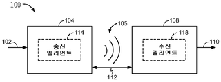
도 1 은 예시적 실시형태에 따른, 무선 전력 전송 시스템 (100) 의 기능 블록도이다. 에너지 전송을 수행하기 위한 무선 (예를 들어, 자기 또는 전자기) 장 (105) 을 생성하기 위해 입력 전력 (102) 이 전원 (본 도에 미도시) 로부터 송신기 (104) 에 제공될 수도 있다. 수신기 (108) 는 무선 장 (105) 에 커플링되고 출력 전력 (110) 에 커플링된 디바이스 (본 도에는 미도시) 에 의한 소비 또는 저장을 위해 출력 전력 (110) 을 발생시킬 수도 있다. 송신기 (104) 및 수신기 (108) 는 거리 112 만큼 분리될 수도 있다. 송신기 (104) 는 수신기 (108) 에 에너지를 송신/커플링하기 위한 전력 송신 엘리먼트 (114) 를 포함할 수도 있다. 수신기 (108) 는, 송신기 (104) 로부터 송신된 에너지를 수신 또는 캡처/커플링하기 위한 전력 수신 엘리먼트 (118) 를 포함할 수도 있다.1 is a functional block diagram of a wireless
일 예시적인 실시형태에서, 송신기 (104) 및 수신기 (108) 는 상호 공진 관계 (mutual resonant relationship) 에 따라 구성될 수도 있다. 수신기 (108) 의 공진 주파수와 송신기 (104) 의 공진 주파수가 실질적으로 같거나 또는 매우 가까울 때, 송신기 (104) 와 수신기 (108) 사이의 송신 손실은 감소된다. 이와 같이, 무선 전력 전송은 더 먼 거리에 대해 제공될 수도 있다. 따라서, 공진 유도 커플링 기법들은 다양한 거리들에 대해 그리고 다양한 유도 전력 송신 및 수신 엘리먼트 구성들로 향상된 효율 및 전력 전송을 허용할 수도 있다.In one exemplary embodiment, the
특정 실시형태에서, 무선 장 (105) 은 송신기 (104) 의 "근접 장" 에 대응할 수도 있다. 근접장은, 전력 송신 엘리먼트 (114) 로부터 멀리 전력을 최소로 방사하는 전력 송신 엘리먼트 (114) 에서의 전류 및 전하로부터 비롯되는 강한 반응성 장이 존재하는 지역에 대응할 수도 있다. 근접장은 전력 송신 엘리먼트 (114) 의 약 1 파장 (또는 그의 몇 분의 1) 내에 있는 지역에 대응할 수도 있다.In certain embodiments, the
특정 실시형태에서, 전자기파로 에너지의 대부분을 원격장 (far field) 에 전파하기보다는 무선 장 (105) 에서 에너지의 대부분을 전력 수신 엘리먼트 (118) 에 커플링시킴으로써, 효율적인 에너지 전송이 일어날 수도 있다.In certain embodiments, efficient energy transfer may occur by coupling most of the energy in the
특정 구현에서, 송신기 (104) 는 전력 송신 엘리먼트 (114) 의 공진 주파수에 대응하는 주파수를 갖는 시변 자기 (또는 전자기) 장을 출력할 수도 있다. 수신기 (108) 가 무선 장 (105) 내에 있을 때, 시변 자기 (또는 전자기) 장은 전력 수신 엘리먼트 (118) 에서 전류를 유도할 수도 있다. 전술된 바처럼, 전력 수신 엘리먼트 (118) 가 전력 송신 엘리먼트 (114) 의 주파수에서 공진하도록 공진 회로로서 구성되면, 에너지가 효율적으로 전송될 수도 있다. 전력 수신 엘리먼트 (118) 에서 유도된 교류 (AC) 신호는 정류되어, 부하에 전력을 공급하거나 또는 충전하기 위하여 제공될 수도 있는 직류 (DC) 신호를 생성할 수도 있다.In certain implementations, the
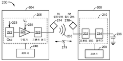
도 2 는 또 다른 예시적 실시형태에 따른, 무선 전력 전송 시스템 (200) 의 기능 블록도이다. 시스템 (200) 은 송신기 (204) 및 수신기 (208) 를 포함할 수도 있다. 송신기 (204) (여기서 전력 전송 유닛, PTU 라고도 함) 는, 오실레이터 (222), 구동기 회로 (224) 및 프론트 엔드 회로 (226) 를 포함할 수도 있는 송신 회로 (206) 를 포함할 수도 있다. 오실레이터 (222) 는, 주파수 제어 신호 (223) 에 응답하여 조절될 수도 있는 원하는 주파수에서 신호를 발생시키도록 구성될 수도 있다. 오실레이터 (222) 는 구동기 회로 (224) 에 오실레이터 신호를 제공할 수도 있다. 구동기 회로 (224) 는, 예를 들어, 입력 전압 신호 (VD) (225) 에 기초하여 전력 송신 엘리먼트 (214) 의 공진 주파수에서 전력 송신 엘리먼트 (214) 를 구동하도록 구성될 수도 있다. 구동기 회로 (224) 는, 오실레이터 (222) 로부터 구형파 (square wave) 를 수신하고 사인파 (sine wave) 를 출력하도록 구성된 스위칭 증폭기일 수도 있다.2 is a functional block diagram of a wireless
프론트 엔드 회로 (226) 는 고조파 또는 다른 원치 않는 주파수를 필터링해내도록 구성된 필터 회로를 포함할 수도 있다. 프론트 엔드 회로 (226) 는 송신기 (204) 의 임피던스를 전력 송신 엘리먼트 (214) 의 임피던스와 정합시키도록 구성된 정합 회로를 포함할 수도 있다. 아래에서 더 상세하게 설명하는 바와 같이, 프론트 엔드 회로 (226) 는 전력 송신 엘리먼트 (214) 와 함께 공진 회로를 생성하기 위한 동조 회로를 포함할 수도 있다. 전력 송신 엘리먼트 (214) 를 구동하는 결과로서, 전력 송신 엘리먼트 (214) 는 배터리 (236) 를 충전시키는데 또는 그렇지 않으면 부하에 전력 공급하는데 충분한 레벨로 전력을 무선으로 출력하기 위하여 무선 장 (205) 을 생성할 수도 있다.Front-
송신기 (204) 는 송신 회로 (206) 의 하나 또는 양태들을 제어하거나 전력의 전송을 관리하는 것과 관련된 다른 동작을 달성하도록 구성된 송신 회로 (206) 에 동작 가능하게 커플링된 제어기 (240) 를 더 포함할 수도 있다. 제어기 (240) 는 마이크로 제어기 또는 프로세서일 수도 있다. 제어기 (240) 는 주문형 집적 회로 (ASIC) 로서 구현될 수도 있다. 제어기 (240) 는 직접 또는 간접적으로 송신 회로 (206) 의 각각의 컴포넌트에 동작 가능하게 접속될 수도 있다. 제어기 (240) 는 또한 송신 회로 (206) 의 각각의 컴포넌트로부터 정보를 수신하고 수신된 정보에 기초하여 계산을 수행하도록 구성될 수도 있다. 제어기 (240) 는 그 컴포넌트의 동작을 조절할 수도 있는 각각의 컴포넌트들에 대한 제어 신호 (예를 들어, 신호 (223)) 를 발생시키도록 구성될 수도 있다. 이와 같이, 제어기 (240) 는 그에 의해 수행된 동작들의 결과에 기초하여 전력 전송을 조절 또는 관리하도록 구성될 수도 있다. 송신기 (204) 는 예를 들어 제어기 (240) 로 하여금 무선 전력 전송의 관리와 관련된 것들과 같은 특정 기능을 수행하게 하는 명령과 같은 데이터를 저장하도록 구성된 메모리 (미도시) 를 더 포함할 수도 있다.The
수신기 (208) (여기서 전력 수신 유닛, PRU 라고도 함) 는, 프론트 엔드 회로 (232) 및 정류기 회로 (234) 를 포함할 수도 있는 수신 회로 (210) 를 포함할 수도 있다. 프론트 엔드 회로 (232) 는 수신 회로 (210) 의 임피던스를 전력 수신 엘리먼트 (218) 의 임피던스와 정합시키도록 구성된 정합 회로를 포함할 수도 있다. 아래에서 설명하는 바와 같이, 프론트 엔드 회로 (232) 는 전력 수신 엘리먼트 (218) 와 함께 공진 회로를 생성하기 위한 동조 회로를 더 포함할 수도 있다. 정류기 회로 (234) 는, 도 2 에 도시된 바처럼, 배터리 (236) 를 충전시키기 위하여 AC 전력 입력으로부터 DC 전력 출력을 발생시킬 수도 있다. 수신기 (208) 및 송신기 (204) 는 추가적으로, 분리된 통신 채널 (219) (예를 들면, 블루투스 (Bluetooth), 지그비 (Zigbee), 셀룰러 등) 상에서 통신할 수도 있다. 다르게는, 수신기 (208) 및 송신기 (204) 는, 무선 장 (205) 의 특성을 사용하여 대역내 시그널링 (in-band signaling) 을 통해 통신할 수도 있다.The receiver 208 (also referred to herein as a power receiving unit, also referred to as a PRU) may include a receiving
수신기 (208) 는 송신기 (204) 에 의해 송신되고 수신기 (208) 에 의해 수신된 전력의 양이 배터리 (236) 를 충전하는데 적절한지 여부를 결정하도록 구성될 수도 있다. 특정 실시형태에서, 송신기 (204) 는 에너지 전송을 제공하기 위해 직접 장 커플링 계수 (k) 를 갖는 주로 비방사성의 장을 발생시키도록 구성될 수도 있다. 수신기 (208) 는 무선 장 (205) 에 직접 커플링되고 출력 또는 수신 회로 (210) 에 커플링된 배터리 (또는 부하) (236) 에 의한 소비 또는 저장을 위해 출력 전력을 발생시킬 수도 있다.The
수신기 (208) 는 무선 전력 수신기 (208) 의 하나 이상의 양태들을 관리하기 위해 전술한 송신 제어기 (240) 와 유사하게 구성된 제어기 (250) 를 더 포함할 수도 있다. 수신기 (208) 는 예를 들어 제어기 (250) 로 하여금 무선 전력 전송의 관리와 관련된 것들과 같은 특정 기능을 수행하게 하는 명령과 같은 데이터를 저장하도록 구성된 메모리 (미도시) 를 더 포함할 수도 있다.The
전술한 바와 같이, 송신기 (204) 및 수신기 (208) 는 거리에 의해 분리될 수도 있고, 송신기 (204) 와 수신기 (208) 사이의 송신 손실을 최소화하기 위해 상호 공진 관계에 따라 구성될 수도 있다.The
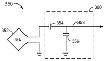
도 3 은 예시적인 구현들에 따른, 도 2의 송신 회로 (206) 또는 수신 회로 (210) 의 일부의 개략도이다. 도 3에 도시된 바와 같이, 송신 또는 수신 회로 (350) 는 전력 송신 또는 수신 엘리먼트 (352) 및 동조 회로 (360) 를 포함할 수도 있다. 전력 송신 또는 수신 엘리먼트 (352) 는 또한 안테나 또는 "루프" 안테나로서 지칭되거나 또는 구성될 수도 있다. 용어 "안테나" 는 일반적으로, 다른 "안테나" 에의 커플링을 위한 에너지를 무선 출력 또는 수신할 수도 있는 컴포넌트를 지칭한다. 전력 송신 또는 수신 엘리먼트 (352) 는 또한 본원에서 "자기" 안테나, 또는 유도 코일, 공진기, 또는 공진기의 일부로서 지칭되거나 또는 구성될 수도 있다. 전력 송신 또는 수신 엘리먼트 (352) 는 또한, 전력을 무선 출력 또는 수신하도록 구성된 일종의 코일 또는 공진기로서 지칭될 수도 있다. 본원에 사용된 바처럼, 전력 송신 또는 수신 엘리먼트 (352) 는, 전력을 무선 출력 및/또는 수신하도록 구성되는 일종의 "전력 전송 컴포넌트" 의 일 예이다. 전력 송신 또는 수신 엘리먼트 (352) 는 페라이트 코어 (본 도에 미도시) 와 같은 물리적 코어 또는 공심 (air core) 을 포함할 수도 있다.FIG. 3 is a schematic diagram of a portion of the transmit
전력 송신 또는 수신 엘리먼트 (352) 가 동조 회로 (360) 를 갖는 공진 회로 또는 공진기로서 구성되는 경우, 전력 송신 또는 수신 엘리먼트 (352) 의 공진 주파수는 인덕턴스 및 커패시턴스에 기초할 수도 있다. 인덕턴스는 단순히 전력 송신 또는 수신 엘리먼트 (352) 를 형성하는 코일 또는 다른 인덕터에 의해 생성된 인덕턴스일 수도 있다. 커패시턴스 (예를 들어, 커패시터) 는 동조 회로 (360) 에 의해 제공되어 원하는 공진 주파수에서 공진 구조를 생성할 수도 있다. 비제한적인 예로서, 동조 회로 (360) 는 커패시터 (354) 를 포함할 수도 있고, 커패시터 (356) 는 송신 및/또는 수신 회로 (350) 에 추가되어 공진 회로를 생성할 수도 있다.When the power transmitting or receiving
동조 회로 (360) 는 전력 송신 또는 수신 엘리먼트 (352) 와 함께 공진 회로를 형성하기 위한 다른 컴포넌트들을 포함할 수도 있다. 또 다른 비제한적인 예로서, 동조 회로 (360) 는 회로 (350) 의 2개의 단자 사이에 병렬로 배치된 커패시터 (미도시) 를 포함할 수도 있다. 여전히 다른 설계가 가능하다. 일부 실시형태에서, 프론트 엔드 회로 (226) 내의 동조 회로는 프론트 엔드 회로 (232) 내의 동조 회로와 동일한 설계 (예를 들어, 360) 를 가질 수도 있다. 다른 실시형태에서, 프론트 엔드 회로 (226) 는 프론트 엔드 회로 (232) 에서와 상이한 동조 회로 설계를 사용할 수도 있다.The
전력 송신 엘리먼트의 경우, 전력 송신 또는 수신 엘리먼트 (352) 의 공진 주파수에 실질적으로 대응하는 주파수를 갖는 신호 (358) 가 전력 송신 또는 수신 엘리먼트 (352) 에 대한 입력일 수도 있다. 전력 수신 엘리먼트의 경우, 전력 송신 또는 수신 엘리먼트 (352) 의 공진 주파수에 실질적으로 대응하는 주파수를 갖는 신호 (358) 가 전력 송신 또는 수신 엘리먼트 (352) 로부터의 출력일 수도 있다. 본 명세서에 개시된 양태들은 일반적으로 공진 무선 전력 전송에 관한 것이지만, 본원에 개시된 양태는 무선 전력 전송을 위한 비공진 구현에 사용될 수도 있음을 당업자는 인식할 것이다.For a power transmitting element, a
도 2에 도시된 전력 송신 엘리먼트 (214) (예를 들어, 송신 코일) 에 주입된 전류의 정확한 측정은 주위로 방사하는 적절한 레벨의 전자기 (EM) 방사를 유지하고, 전력 전송 특성 등을 측정하는데 사용될 수도 있다. 일부 해결책들은 (예를 들어, 차동 증폭기를 사용하여) 2개의 직렬 커패시터에 걸친 전압 강하를 측정하는 것에 기초할 수도 있으며, 하나의 커패시터는 송신 코일의 각각의 코일 리드에 부착된다. 이러한 방식으로 전압을 직접 측정하면 코일 리드가 모두 고전압이기 때문에 차동 전압 버퍼 및 차동 증폭기를 포함하는 증폭기 회로의 설계와 관련된 기술적 어려움이 생길 수 있다. 또한, 이러한 측정 프로세스는, 직렬 캐패시터 뒤의 전력 송신 엘리먼트 (214) 에 걸친 전압의 측정, 그리고 다음으로 직렬 캐패시터 이후의 전압의 측정을, 저역 필터에 공급하는 전압의 빠른 스위칭 등과 함께, 필요로 하므로, 복잡할 수 있다. 회로는 구현하기에 값비싼 컴포넌트들이 필요할 수도 있고; 그리고 측정 프로세스는 전력 송신 엘리먼트 (214) 에 주입될 수 있는 스위칭 노이즈로 인해서 상당한 양의 전자파 간섭 (EMI) 을 생성할 수 있다.Accurate measurement of the current injected into the power transmission element 214 (e.g., the transmit coil) shown in Figure 2 maintains an appropriate level of electromagnetic (EM) radiation that radiates around, . Some solutions may be based on measuring the voltage drop across two series capacitors (e.g., using a differential amplifier), with one capacitor attached to each coil lead of the transmit coil. Direct measurement of voltage in this manner can cause technical difficulties related to the design of amplifier circuits, including differential voltage buffers and differential amplifiers, because the coil leads are all high voltage. This measurement process also requires a measurement of the voltage across the power transmission element 214 behind the series capacitor, and then a measurement of the voltage after the series capacitor, along with a fast switching of the voltage supplying the low pass filter , It can be complicated. Circuits may require expensive components to implement; And the measurement process may generate a significant amount of electromagnetic interference (EMI) due to the switching noise that may be injected into the power transmitting element 214.
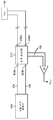
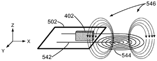
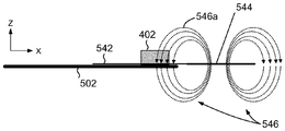
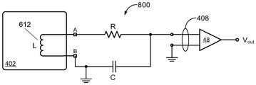
도 4a 및 도 4b를 참조하면, 부하에 주입되는 전류를 측정하는데 사용될 수도 있는 본 개시에 따른 전류 센서에 대해 이제 설명될 것이다. 도 4a 는 전류 운반 도체 (42) 를 통해 부하 (44)에 접속된 전력 증폭기 (40) 를 포함하는 회로를 도시한다. 본 개시에 따른 전류 센서 (402) 는 전류 운반 도체 (42) 에서 전류의 흐름을 감지하고 전류 운반 도체 (42) 에서 전류의 흐름을 나타내는 신호를 생성하도록 구성될 수도 있다.4A and 4B, a current sensor according to the present disclosure, which may be used to measure current injected into a load, will now be described. 4A shows a circuit including a
단지 사용 사례를 설명하기 위한 예로서, 전류 센서 (402) 는 도 2에 도시된 무선 전력 전송 시스템 (200) 에 통합될 수도 있다. 이 예에서, 전력 증폭기 (40) 는 송신기 (204) 에서 구동기 회로 (224) 에 대응할 수도 있고, 부하 (44) 는 전력 송신 엘리먼트 (214) (예를 들어, 송신 코일) 에 대응할 수도 있다. 전류 센서 (402) 는 전력 송신 엘리먼트 (214) 에 의해 발생된 자기장을 통해 수신기 (208) (예를 들어, PRU) 에 커플링되고 있는 전력의 양의 변동의 결과로서 무선 전력 전송 동안 전력 송신 엘리먼트 (214) 의 부하 변화를 검출할 수도 있다. 예를 들어, 전력 커플링의 변동은 PRU가 인출하는 전력의 양, 송신기 (204) 와의 무선 전력 전송에 관여하는 PRU의 수 등으로부터 비롯될 수도 있다. 전류 운반 도체 (42) 는 구동기 회로 (224) 로부터 전력 송신 엘리먼트 (214) 로 전류를 제공하는 접속부 (예를 들어, 미도시 와이어) 에 대응할 수도 있다. 물론, 본 개시에 따른 전류 센서 (402) 는 다른 회로들에서의 사용을 위해 용이하게 적합화될 수도 있다는 것이 이해될 것이다.As an example only to illustrate the use case, the
전류 센서 (402) 는 전류 운반 도체 (42) 에 대한 접속 지점을 제공하기 위한 접속부 (404 및 406) 를 포함할 수도 있다. 전류 센서 (402) 는 도체 (42) 에서의 전류의 흐름에 응답하여 감지된 신호를 출력하기 위한 출력부 (408) 를 포함할 수도 있다. 출력부 (408) 는 예를 들어, 전류 운반 도체 (42) 에서 전류의 흐름을 나타내거나 그렇지 않으면 표시하는 출력 신호 (Vout) 를 생성하기 위해, 증폭기 (48) 와 같은 감지된 신호로부터 출력 신호를 발생시키는 수단에 접속될 수도 있다. 일부 실시형태에서, 증폭기 (48) 의 출력은 전류 운반 도체 (42) 에서의 전류의 흐름을 나타내는 전류 신호일 수도 있다. 도 4a에 도시된 것과 같은 다른 실시형태에서, 증폭기 (48) 의 출력은 전류 운반 도체 (42)에서의 전류의 흐름을 나타내는 출력 전압 (Vout) 일 수도 있다. 일부 실시형태에서, 증폭기 (48) 의 출력은 전력 증폭기 (40) 로부터 전류의 흐름을 제어하기 위해 피드백 신호로서 사용될 수도 있다. 다른 실시 형태들에서, 증폭기 (48) 의 출력은 시스템의 동작 상황을 모니터링하는데 사용될 수도 있다. 예를 들어, 도 2에 도시된 무선 전력 전송 시스템 (200) 의 맥락에서, 일부 실시형태에서, 전류 센서 (402) 는 과부하 상태를 검출하는데 사용될 수도 있다. 다른 실시형태들에서, 전류 센서 (402) 는 송신기 (204) 의 충전 표면 상에 PRU 의 배치를 검출하는 것 등에 사용될 수도 있다.The
도 4a 에서의 전력 증폭기 (40) 는 단일 엔드형 출력의 예를 나타낸다. 도 4b를 참조하면, 일부 실시형태에서, 전력 증폭기 (40a) 는 2개의 전류 운반 도체 (42a 및 42b) 를 사용하여 전력을 제공하도록 구성된 차동 출력부를 가질 수도 있다. 따라서, 본 개시의 일부 실시형태에 따른 전류 센서 (412) 는 다수의 전류 운반 도체 (예를 들어, 42a, 42b) 상의 전류 감지를 제공하도록 구성될 수도 있다. 일부 실시형태들에서, 예를 들어, 전류 센서 (412) 는 전류 운반 도체 (42a, 42b) 에 대한 접속 지점을 제공하기 위한 접속부 (404a, 404b 및 406a, 406b) 를 포함할 수도 있다.The
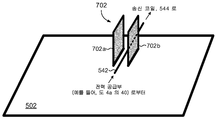
도 5a는 본 개시에 따라 구성된 전류 센서 (402) 를 도시한다. 전류 센서 (402) 는 회로 판 (502) 상에 배치될 수도 있다. 일부 실시형태에서, 예를 들어, 회로 판 (502) 은 무선 전력 전송 시스템 (예컨대, 도 2) 의 전력 송신 유닛 (예를 들어, 도 2의 송신기 (204)) 내의 전자 컴포넌트일 수도 있다. 전류 센서 (402) 는 회로 판 (502) 상에 지지된 도체 (542) 에 인접하게 또는 근접하게 배치되거나 또는 그렇지 않으면 위치될 수도 있다. 일부 실시형태에서, 도체 (542) 는 회로 판 (502) 에 부착된 와이어일 수도 있다. 다른 실시형태에서, 도체 (542) 는 회로 판 (502) 상에 형성된 트레이스 등일 수도 있다.5A shows a
도체 (542) 는 무선 전력 전송 시스템의 송신 코일 (544) 에 접속될 수도 있다. 일부 실시형태에서, 전류 센서 (402) 는 전원 (예를 들어, 도 4a의 전력 증폭기 (40)) 의 하이 사이드 (high side) 에서 도체 (542) 에 인접하게 배치될 수도 있다. 예를 들어, 도체 (542) 는 전원의 출력부와 송신 코일 (544) 사이에 접속될 수도 있다. 다른 실시형태에서, 전류 센서 (402) 는 도체 (542) 의 로우 사이드 (low side) 에 위치될 수도 있다. 예를 들어, 도체 (542) 는 송신 코일 (544) 과 접지 사이에 접속될 수도 있다. 일부 실시 형태에서, 도체 (542) 에서의 전압은 수십 볼트일 수 있기 때문에, 전류 센서 (402) 를 도체 (542) 의 로우 사이드에 배치하면 전압을 2 내지 3 자릿수의 비율로 (by a factor of two to three orders of magnitude) 감소시킬 수 있으며, 따라서 전류 센서 (402) 에서 유도된 전압을 감소시킬 수 있다.The
본 개시에 따르면, 전류 센서 (402) 는, 역선이 전류 센서 (402) 의 최소 단면 영역과 교차하도록, 무선 전력 전송 동작 중에 송신 코일 (544) 에 의해 발생될 수 있는 자기 장 (546) 에 대해, 배향될 수도 있다. 일부 실시 형태들에서, 예를 들어, 전류 센서 (402) 는 자기 장 (546) 의 일부 역선 (플럭스) 에 평행한 평면에 배향될 수도 있다. 도 5a에 도시된 특정 실시형태에서, 예를 들어, 송신 코일 (544) 은 회로 판 (502) 과 동일한 평면에 배향된다. 따라서, 자기장 (542) 이 송신 코일 (544) 에 수직할 것이기 때문에, 전류 센서 (402) 는 회로 판 (502) 에 대해 수직으로 배치된다. 다른 실시 형태들에서, 송신 코일 (544) 은 회로 판 (502) 에 대해 수직하지 않은 각도로 놓일 수도 있다. 따라서, 전류 센서 (402) 는 송신 코일 (544) 로부터 자기장 (546) 의 역선에 평행한 평면으로 배향되도록 적절한 각도로 회로 판 (502) 에 부착될 것이다.According to the present disclosure, the
도 5b의 평면도 및 도 5c의 상면도는 본 개시에 따른 전류 센서 (402) 와 자기장 (546) 간의 상대적인 배향을 더 나타낸다. XYZ 좌표는 기준 (reference) 을 확립하는데 사용된다. 일부 실시형태에서 예를 들어, 일반성의 손실없이, 회로 판 (502) 및 송신 코일 (544) 은 XY 평면에 놓인다. 따라서, 전류 센서 (402) 는 XZ 평면에 배향된다. 도 5b의 평면도는 XZ 평면에 놓인 자기장 (546) 의 특정 역선 (546a) 을 도시하고, 전류 센서 (402) 의 배향은 또한 이들 역선 (546a) 에 평행한 평면에 있다. 역선 (546a) 에 대한 전류 센서 (402) 의 배향은 도 5c에 도시된 상면도에 더 나타나있다.The top view of FIG. 5B and the top view of FIG. 5C further illustrate the relative orientation between
도 6은 본 개시에 따른 전류 센서 (402) 의 상세를 문맥을 위해 도 4a에 도시된 일부 회로 엘리먼트들과 함께 도시한다. 삽입도는 뷰 라인 A-A를 따라 취한 뷰를 나타낸다. 도체 (542) 는 전력 공급부 (예를 들어, 도 4a의 전력 증폭기 (40)) 을 송신 코일 (544) 에 접속시킬 수도 있다. 삽입도에서 볼 수 있는 바와 같이, 도체 (542) 및 전류 센서 (402) 는 전술한 바와 같이 회로 판 (502) 상에 배치될 수도 있다. 도 5a 에 확립된 XYZ 좌표 기준은 회로 판 (502) 상의 전류 센서 (402) 및 도체 (542) 의 상대적인 배향을 나타낸다.Figure 6 shows the details of the
일부 실시형태에서, 전류 센서 (402) 는 예를 들어, 기판 (632) 에 의해 정의된 바와 같이 평면 상에 배치된 감지 엘리먼트 (604) 를 포함할 수도 있다. 감지 엘리먼트 (604) 는 도전성 재료의 코일 (612) (또는 루프) 을 포함할 수도 있다. 기판 (632) 은 인쇄 회로 판 (PCB) 일 수도 있다. 코일 (612) 은 기판 (632) 상에 형성된 트레이스 (trace) 또는 복수의 트레이스 세그먼트일 수도 있다. 코일 (612) 에 사용된 전도성 재료는 구리 또는 임의의 적합한 도전성 재료일 수도 있다. 전도성 재료는 다수의 공지된 기술 중 임의의 것을 사용하여 기판 (632) 상에 형성되거나 또는 그렇지 않으면 성막될 수도 있다.In some embodiments, the
도 6 은 기판 (632) 의 제 1면 상에 형성된 코일 (612) 을 도시한다. 일부 실시형태에서, 코일 (612) 은 하나 이상의 턴 (turn) 을 가질 수도 있다. 코일 (612) 의 외측 단부 (612b) 는 기판 (632) 상의 전도성 패드 (B) 에서 종결될 수도 있다. 코일 (612) 의 내측 단부 (612a) 는 기판 (632) 을 통해 형성된 비아들 (614 및 618) 및 비아 (614) 를 비아 (618) 에 접속시키는 기판 (632) 의 제 2 면 상에 형성된 트레이스 (616) 를 포함하는 복귀 경로에 의해 기판 (632) 상에 전도성 패드 (A) 에서 종결된다. 트레이스는 비아 (618) 를 패드 (A) 에 접속시킬 수도 있다. 패드 (A, B) 에는 증폭기 (예를 들어, 도 4a 의 48) 가 접속될 수도 있다.6 shows a
본 개시에 따르면, 전류 센서 (402) 는 예를 들어, 도체 (542) 근처에 위치된 전류 센서 (402) 에 의해, 감지 엘리먼트 (604) 및 도체 (542) 에 인접하게 배치된 용량성 차폐부 (622) 를 더 포함할 수도 있다. 일부 실시형태에서, 용량성 차폐부 (622) 는 기판 (632) 상에 형성된 전도성 트레이스 (리드) 를 포함할 수도 있다. 용량성 차폐부 (622) 의 일 단부 (622a) 는 "자유 (free)" 이거나 또는 달리 접속되지 않을 수도 있다. 용량성 차폐부 (622) 의 또 다른 단부 (622b) 는 트레이스 (624) 를 통해 전도성 패드 (C) 에 전기적으로 접속될 수도 있다. 일부 실시형태에서, 패드 (C) 는 접지 전위에 접속될 수도 있다. 다른 실시형태에서, 패드 (B) 및 패드 (C) 는 공통 전압 기준에 접속될 수도 있다. 이하, 본 개시의 양태를 설명한다.According to the present disclosure, the
동작시, 도 5a 및 도 6을 참조하여, AC 구동 전류가 송신 코일 (544) 을 구동하기 위해 제공될 때, 도체 (542) 를 통한 전류의 흐름은 자기장 (548) (도 6의 삽입도) 을 전류 센서 (402) 근처의 도체 (542) 내 제 1 위치에서 발생시킬 수 있다. Y-Z 평면에 있는 자기장 (548) 은 일반적으로 X-Z 평면에 있는 자기장 (546) (예를 들어, 도 5b) 에 직교한다. 전류 센서 (402) 의 감지 엘리먼트 (604) 컴포넌트는 자기장 (548) 에 커플링하는 수단의 역할을 할 수 있으며, 이는 차례로, 감지 엘리먼트 (604) 에서 유도된 전류의 흐름 (감지된 신호) 을 초래할 수 있다. 감지 엘리먼트 (604) 에서 발생된 감지된 신호는 단부 (612a, 612b) 에서 제공될 수 있고 증폭기 (48) 에 의해 증폭되어 도체 (542) 를 통해 흐르는 전류의 양을 나타내는 출력 신호 (Vout) 를 생성할 수 있다.5A and 6, when an AC drive current is provided to drive the transmit
전술한 바와 같이, 전류 센서 (402) 는 전류를 운반하는 도체 (542) 와 감지 엘리먼트 (604) 를 포함하는 코일 (612) (측정 루프) 사이의 자기적 커플링에 기초한다. 따라서, 도체 (542) 와 감지 엘리먼트 (604) 사이의 커플링의 증가는 감지된 신호의 신호 대 잡음비 (SNR) 를 향상시킬 수 있다. 그러나, 동시에, 감지 신호의 부정확성을 피하기 위해 감지 엘리먼트 (604) 와 임의의 다른 자기장 소스 간의 자기적 커플링의 감소가 바람직할 수도 있다.As discussed above, the
일부 실시형태에서, 송신 코일 (544) 은 전류 센서 (542) 를 지니는 회로 판 (502) 에 물리적으로 근접할 수도 있다. 그 결과, 전류 센서 (402) 는 예를 들어, 무선 전력 전송 동작 동안 송신 코일 (544) 에 의해 발생된 자기장 (546) 에 노출될 수 있다. 한편으로, 이러한 외부적으로 발생된 자기장 (546) 은 전류에 비례하기 때문에, 전류 센서 (402) 의 감지 엘리먼트 (604) 에서 결과적인 유도 전류 흐름 (감지된 신호) 은 SNR을 향상시킬 수도 있다. 다른 한편, 송신 코일 (544) 에 의해 발생된 자기장 (546) 은 자기장 부근의 전력 수신 디바이스 및 다른 디바이스들의 영향을 받을 수 있다. 따라서, 자기장 (546) 의 이러한 변동은 전류 센서 (402) 에 대한 에러의 원인이 될 수 있다. 자기장 (546) 이 (예를 들어, 수신기 측에서 변하는 부하 상황으로 인해) 변하지만 도체 (542) 에 흐르는 전류가 일정하면 에러가 두드러질 수 있다. 환언하면, 자기장 (546) 의 변동은 도체 (542) 에서의 전류 흐름이 일정하더라도 출력 신호 (Vout) 의 변동을 생성할 수 있다. 전류 센서 (402) 는 피드백을 제공하여 자기장 (546) 을 조절하거나 또는 자기장 (546) 내에 이물질을 검출하는데 사용될 수도 있기 때문에, 자기장 (546) 이 감지된 신호와 간섭하지 않도록 보장하는 것이 유리할 수도 있다.In some embodiments, the transmit
본 개시에 따르면, 예를 들어, 도 5a 내지 도 5c에 나타낸 바와 같이, 자기장 (546) 의 자기 차폐 (magnetic shielding) 는 송신 코일 (544) 에 의해 발생된 플럭스와 평행하게 감지 엘리먼트 (604) 를 배향시킴으로써 달성될 수 있다. 일부 구현에서, 예를 들어, 회로 판 (502) 은 송신 코일 (544) 과 동일한 평면 내에 있다. 따라서, 이러한 구현에서 감지 엘리먼트 (604) 는 회로 판 (502) 에 수직으로 배향된다.According to the present disclosure, magnetic shielding of a
본 개시에 따라 송신 코일 (544) 에 상대적으로 감지 엘리먼트 (604) 를 배향시키는 것은 자기장 (546) 의 역선에 의해 교차되는 감지 엘리먼트 (604) 의 단면 영역을 최소화할 수 있다는 것이 인식될 수 있다. 교차된 단면 영역을 최소화함으로써, 송신 코일 (544) 에 의해 발생된 자기장 (546) 의 유도 전류 효과를 최소화하고, 따라서 감지 엘리먼트 (604) 에서 감지된 신호에 대한 자기장 (546) 의 변동 효과를 최소화한다.It can be appreciated that orienting the
도 5a 및 도 6을 계속 참조하면, 전류가 도체 (542) 를 통해 흐르는 경우 위에서 설명한 바와 같이, 자기장 (548) (도 6의 삽입도 참조) 이 도체 (542) 로부터 비롯될 수도 있다. 도체 (542) 의 부근에 있는 감지 엘리먼트 (604) 는 자기장 (548) 에 자기적 커플링할 수도 있다. 감지 엘리먼트 (604) 및 도체 (542) 부근의 영역은 감지 영역으로 지칭될 수도 있다. 자기장 (548) 에 자기적 커플링하는 것으로부터 비롯되는 전압이 감지 엘리먼트 (604) 에서 유도될 수도 있다. 유도 전압은 도체 (542) 에 흐르는 전류를 나타내는 출력 전압 (Vout) 을 발생시키기 위해 증폭기 (48) 에 의해 증폭될 수도 있다.5A and 6, magnetic field 548 (see also the inset of FIG. 6) may originate from
감지 엘리먼트 (604) 에의 도체 (542) 의 근접은 커패시터를 생성할 수 있다. 송신 코일 (544) 이 고주파에서 고전압에 의해 구동되는 경우, 커패시턴스가 작을 수 있더라도 도체 (542) 와 감지 엘리먼트 (604) 사이의 용량성 커플링이 현저할 수도 있다. 예를 들어, 일부 실시형태에서, 송신 코일 (544) 은 수십 볼트 정도로 6.78MHz 신호에 의해 구동될 수도 있다. 결과적으로, 감지 엘리먼트 (604) 로의 도체 (542) 의 전위에 의해 발생된 전기장의 용량성 커플링이 현저할 수 있다. 감지 엘리먼트 (604) 에 커플링될 수 있는 에너지는 발생된 출력 전압 (Vout) 에서 에러를 생성할 수 있다.Proximity of the
본 발명에 따르면, 도체 (542) 와 감지 엘리먼트 (604) 사이의 용량성 차폐부 (622) 가 전기장 격리 (electric field isolation) 를 제공할 수 있다. 용량성 차폐부 (622) 는 전기장을 접지 전위에 용량성으로 커플링함으로써 감지 엘리먼트 (604) 로부터 전기장을 격리시킬 수 있으며, 따라서 도체 (542) 에 의해 발생된 전기장의 영향으로부터 출력 전압 (Vout) 을 차폐한다.According to the present invention, the
도 6a는 본 개시의 일부 실시형태에 따른 전류 센서 (402') 를 도시한다. 일부 실시형태에서, 전류 센서 (402') 는, (예를 들어, 기판 (632-1) 에 의해 정의된 바와 같은) 제 1 평면 상에 배치된 전도성 재료 (612-1) 의 제 1 코일 (또는 루프) 및 (예를 들어, 기판 (632-2) 에 의해 정의된 바와 같은) 제 2 평면 상에 배치된 전도성 재료 (612-2) 의 제 2 코일을 포함하는 감지 엘리먼트 (604) 를 포함할 수도 있다.6A shows a current sensor 402 'in accordance with some embodiments of the present disclosure. In some embodiments, the current sensor 402 'includes a first coil (not shown) of the conductive material 612-1 disposed on a first plane (e.g., as defined by the substrate 632-1) Or loop) and a second coil of a conductive material 612-2 disposed on a second plane (e.g., as defined by substrate 632-2) You may.
일부 실시형태에서, 기판 (632-1, 632-2) 은 다층 PCB (632') 내 층일 수도 있다. 코일 (612-1, 612-2) 은 PCB (632') 의 각 층 상에 형성된 트레이스일 수도 있다. 코일 (612-1, 612-2) 을 형성하는데 사용되는 전도성 재료는 구리 또는 임의의 적절한 재료일 수도 있다. 트레이스는 다수의 공지된 기술 중 임의의 것을 사용하여 기판 (632-1, 632-2) 상에 형성될 수도 있다.In some embodiments, the substrates 632-1 and 632-2 may be layers in a multi-layer PCB 632 '. Coils 612-1 and 612-2 may be traces formed on each layer of PCB 632 '. The conductive material used to form the coils 612-1 and 612-2 may be copper or any suitable material. The traces may be formed on the substrates 632-1 and 632-2 using any of a number of known techniques.
일부 실시형태에서, 코일 (612-1, 612-2) 은 예를 들어 도 6a에 도시된 바와 같이 직렬로 접속될 수도 있다. 코일 (612-1) 의 외측 단부 (612-1b) 는 기판 (632-1) 상의 전도성 패드 (B) 에서 종결될 수도 있다. 비아 (614b) 는 기판 (632-1) 상의 코일 (612-1) 의 내측 단부 (612-1a) 를 기판 (632-2) 상의 코일 (612-2) 의 내측 단부 (612-2a) 에 접속시키는 역할을 할 수도 있다. 비아 (614c) 는 기판 (632-2) 상의 코일 (612-2) 의 외측 단부 (612-2b) 를 기판 (632-1) 상의 전도성 패드 (A) 에 접속시킬 수도 있다.In some embodiments, the coils 612-1 and 612-2 may be connected in series, for example, as shown in Fig. 6A. The outer end 612-1b of the coil 612-1 may terminate at the conductive pad B on the substrate 632-1. The via 614b connects the inner end 612-1a of the coil 612-1 on the substrate 632-1 to the inner end 612-2a of the coil 612-2 on the substrate 632-2 It can also play a role. The via 614c may connect the outer end 612-2b of the coil 612-2 on the substrate 632-2 to the conductive pad A on the substrate 632-1.
본 개시에 따르면, 전류 센서 (402') 는 감지 엘리먼트 (604) 의 코일 (612-1) 과 도체 (542) 양자 모두에 인접하여 배치된 제 1 용량성 차폐부 (622-1) 및, 전류 센서 (402') 가 도체 (542) 에 근접 배치됨으로써 감지 엘리먼트 (604) 의 코일 (612-2) 및 도체 (542) 에 인접하게 배치된 제 2 용량성 차폐부 (622-2) 를 더 포함할 수도 있다. 일부 실시형태에서, 제 1 용량성 차폐부 (622-1) 는 기판 (632-1) 상에 형성된 전도성 트레이스 (리드) 를 포함할 수도 있고, 마찬가지로 제 2 용량성 차폐부 (622-2) 는 기판 (632-2) 상에 형성된 전도성 트레이스 (리드) 를 포함할 수도 있다.According to the present disclosure, the current sensor 402 'includes a first capacitive shield 622-1 disposed adjacent to both the coil 612-1 and the
본 개시에 따르면, 용량성 차폐부 (622-1, 622-2) 는 함께 접속되어 각각의 용량성 차폐부가 자유 단부와 접지된 단부를 가지므로, 용량성 차폐부는 폐쇄 루프를 형성하지 않는다. 도 6a는 일부 실시형태에 따른 접속 구성을 도시한다. 용량성 차폐부 (622-1) 의 일 단부 (622-1a) 는 "자유" 이거나 또는 달리 접속되지 않을 수도 있다. 용량성 차폐부 (622-1) 의 다른 단부 (622-1b) 는 예를 들어 트레이스 (624) 를 통해 전도성 패드 (C) 에 접속될 수도 있다. 마찬가지로, 용량성 차폐부 (622-2) 의 일 단부 (622-2a) 는 "자유 (free)" 이거나 또는 달리 접속되지 않을 수도 있다. 용량성 차폐부 (622-2) 의 다른 단부 (622-2b) 는 전도성 패드 (C) 에 접속될 수도 있으며; 예를 들어, 비아 (614a) 는 단부 (622-2b) 를 단부 (622-1a) 에 접속시킬 수도 있다. 일부 실시형태에서, 패드 (C) 는 접지 전위에 접속될 수도 있다. 다른 실시형태에서, 패드 (B) 및 패드 (C) 는 공통 전압 기준에 접속될 수도 있다.According to the present disclosure, capacitive shields 622-1 and 622-2 are connected together and each capacitive shield has a free end and a grounded end, so that the capacitive shield does not form a closed loop. 6A shows a connection configuration according to some embodiments. One end 622-1a of capacitive shield 622-1 may be "free" or otherwise not connected. The other end 622-1b of the capacitive shield 622-1 may be connected to the conductive pad C via, for example, a
도 6b는 본 개시의 일부 실시형태에 따른 전류 센서 (402") 를 도시한다. 도 6b에 도시된 구성에서, 용량성 차폐부 (622-1, 622-2) 는 연속적인 트레이스를 형성하도록 엔드 투 엔드 (end-to-end) 방식으로 접속될 수도 있다. 예를 들어, 용량성 차폐부 (622-2) 의 일 단부 (622-2b) 는 자유 단부일 수도 있다. 용량성 차폐부 (622-2) 의 타 단부 (622-2a) 는 예를 들어 비아 (614a) 를 사용하여, 용량성 차폐부 (622-1) 의 일 단부 (622-1a) 에 접속할 수도 있다. 용량성 차폐부 (622-1) 의 타 단부 (622-1b) 는 예를 들어 트레이스 (624) 를 사용하여 패드 (C) 에 접속될 수도 있다. 당업자는 본 개시에 따른 또 다른 접속 구성이 가능할 수도 있음을 이해할 것이다.6B illustrates a
본 개시에 따라, 도 6a 또는 도 6b 에서의 감지 엘리먼트 (604) 는 코일 (612-1, 612-2) 이외에 다층 PCB (632') 의 각각의 추가 층 상에 제공된 코일을 포함할 수도 있음을 당업자는 인식할 것이다. 일부 실시형태에서, 예를 들어, PCB (632') 는 N개의 코일을, 각 층에 하나의 코일씩, 포함하는 감지 엘리먼트 (604) 를 지지하는 N 층 PCB 일 수도 있다. 각각의 추가 코일을 수반하는 것은 동일한 층 상의 코일에 인접하게 배치된 (예를 들어, 코일과 공면의) 용량성 차폐부 (트레이스 리드) 일 수도 있다.According to the present disclosure, the
도 7은 본 개시의 일부 실시형태에 따른 전류 센서 (702) 를 도시한다. 일부 실시형태에서, 회로 판 (502) 상에 배치된 전류 센서 (702) 는 도체 (542) 에서 전류 흐름을 감지하기 위한 이중 구조를 가질 수도 있다. 전류 센서 (702) 는 제 1 센서 컴포넌트 (702a) 및 제 1 센서 컴포넌트 (702a) 로부터 이격된 제 2 센서 컴포넌트 (702b) 를 포함할 수도 있다. 전류 센서 (702) 는 제 1 센서 컴포넌트 (702a) 가 도체 (542) 의 일측에 놓이고 제 2 센서 컴포넌트 (702b) 가 도체 (542) 의 타측 상에 제 1 센서 컴포넌트 (702a) 에 대향하게 놓이도록 도체 (542) 에 걸쳐 있을 수도 있다. 제 1 센서 컴포넌트 (702a) 내의 감지 엘리먼트 (예를 들어, 도 6 의 604) 는, 제 2 센서 컴포넌트 (702b) 내의 감지 엘리먼트를 포함하는 코일의 권선과, 시계 방향 또는 반시계 방향의 어느 일방으로, 동일한 방향으로 감겨진 코일 (예를 들어, 도 6 의 612) 을 포함할 수도 있다. 제 1 및 제 2 센서 컴포넌트들 (702a, 702b) 내의 각각의 코일들은 함께 접속되어 각각의 코일들에서 전류 흐름을 합산할 수도 있다. 이러한 이중 구조는 도 6에 도시된 단일 구조 전류 센서 (402) 와 비교하여 증가된 전류 감지 감도를 제공할 수 있다.Figure 7 shows a
도 8은 본 개시에 따라 감지된 신호를 필터링하는 수단 (800) 을 나타낸다. 먼저, 도 6a를 잠시 참조하면, 도체 (542) 에서 전류 흐름을 측정하는 것은 감지 엘리먼트 (612) 에 유도된 감지된 신호의 파형의 RMS (root mean square) 를 결정하는 것을 수반할 수도 있다. RMS는 감지된 신호에서 피크를 측정하고 제로 크로싱 (zero crossing) 을 검출하여 위상 각을 결정함으로써 결정될 수도 있다. 그러나, 이러한 접근법은 감지된 신호의 파형이 고조파를 갖지 않아야 한다는 제약이 있다.FIG. 8 shows means 800 for filtering a sensed signal in accordance with the present disclosure. 6A, measuring current flow in
고조파의 소스는 도체 (542) 에서 전류를 제공하는 전력 증폭기 (예를 들어, 40, 도 4a) 에서 비롯될 수 있다. 일부 구현에서, 전력 증폭기는 비선형 증폭기일 수도 있다. 예를 들어, 무선 전력 시스템의 고전력 출력 요건 및 비용 제약은 비선형 설계에 영향을 줄 수도 있다. 비선형 전력 증폭기에 의해 생성되는 전류 및 전압은 전형적으로 상당한 고조파 성분을 갖는다.The source of the harmonic may originate from a power amplifier (e.g., 40, FIG. 4A) that provides current in
본 개시에 따르면, 대역통과 필터는 전류 측정을 위해 전류 센서 (402) 의 출력 (408) 에서 더 높은 고조파 및 더 낮은 고조파를 필터링해내기 위해 감지된 신호에 대해 사용될 수도 있다. 도 8은 본 개시의 일부 실시형태에 따라 감지된 신호를 필터링하는 수단 (800) 을 도시한다. 위에서 설명된 바처럼, 감지 엘리먼트 (604) (도 6) 는 도전성 재료의 코일 (612) (또는 루프) 을 포함한다. 따라서, 코일 (612) 은 인덕턴스 L 을 갖는다. 코일 (612) 은 저항 R 및 캐패시터 C 를 사용하여 대역통과 필터 (800) 를 생성하는데 사용될 수 있다. 예를 들어, 저항 R 은 전류 센서 (402) 상의 패드 A (도 6) 와 증폭기 (48) 에 대한 입력 사이에 접속될 수도 있다. 커패시터 C 는 증폭기 (48) 에 대한 다른 입력과 패드 B 사이에 접속될 수도 있다. C의 값은 코일 (612) 의 인덕턴스 L 및 전력 공급부의 동작 주파수에 기초하여 결정될 수도 있다. 예를 들어, 일부 구현에서, 동작 주파수는 무선 전력 전송 시스템에서 송신 코일 (544) 의 공진 주파수일 수도 있다. 저항 R 은 대역통과 필터 (800) 를 디튜닝하고 실제 성분 값에 대한 감도를 감소시키기 위해 대역통과 주파수를 넓히기 위해 부가될 수 있는 작은 저항일 수도 있다.According to the present disclosure, a bandpass filter may be used for the sensed signal to filter higher harmonics and lower harmonics at the
전압 측정을 위해, 용량성 전압 분배기 (미도시) 가 사용될 수도 있다. 원하는 고조파 제거를 달성하기 위해, 예를 들어, 7차 4단 버터워스 필터 (7th order, 4-stage Butterworth filter) (미도시) 가 사용될 수도 있다. 임의의 적절한 대역통과 필터 설계가 사용될 수도 있다는 것을 이해할 것이다.For voltage measurement, a capacitive voltage divider (not shown) may be used. To achieve the desired harmonic rejection, for example, a 7th order, 4-stage Butterworth filter (not shown) may be used. It will be appreciated that any suitable bandpass filter design may be used.
도 9는 본 개시의 일부 실시형태에 따른 전류 센서 (902) 를 도시한다. 일부 실시형태에서, 전류 센서 (902) 는 예를 들어, 기판 (932) 에 의해 정의된 바와 같이 평면 상에 배치된 감지 엘리먼트 (904) 를 포함할 수도 있다. 감지 엘리먼트 (904) 는 제 1 전도성 재료 코일 (912-1) 및 제 2 전도성 재료 코일 (912-2) 을 포함할 수도 있다. 제 1 및 제 2 코일 (912-1, 912-2) 은 직렬로 접속될 수도 있다. 예를 들어, 비아들은 제 1 및 제 2 코일 (912-1, 912-2) 을 직렬로 접속시키기 위해 기판 (932) 의 반대 면 상에 트레이스들을 라우팅하는데 사용될 수도 있다.Figure 9 shows a
일부 실시형태에서, 감지 엘리먼트 (904) 를 포함하는 제 1 및 제 2 코일 (912-1, 912-2) 은 기판 (932) 상에 실질적으로 공면을 이루고, 서로 대향 관계에 있을 수도 있다. 본 개시에 따르면, 감지 엘리먼트 (904) 는 코일 (912-1, 912-2) 과 역선 사이의 교차 영역을 최소화하도록 송신 코일 (544) 에 의해 발생된 자기장의 역선에 대해 배향될 수도 있다. 일부 실시형태에서, 예를 들어, 감지 엘리먼트 (904) 는 송신 코일 (544) 에 의해 발생된 자기장의 역선에 평행한 평면에 배향될 수도 있다.In some embodiments, the first and second coils 912-1 and 912-2, including the
전원 (예를 들어, 도 4a 의 전력 증폭기 (40)) 으로부터 송신 코일 (544) 에 구동 전류를 제공하는 도체 (542) 는 기판 (932) 의 표면을 따라 걸쳐있는 세그먼트 (542-1) 를 가질 수도 있다. 도체 세그먼트 (542-1) 는 코일 (912-1, 912-2) 사이에 걸쳐있을 수도 있다. 전류가 도체 (542), 그리고 따라서 도체 세그먼트 (542-1) 를 통해 (예를 들어, 무선 전력 전송 동안) 흐를 때, 자기장이 발생될 수 있다. 차례로, 자기장은 양쪽 모두의 코일 (912-1, 912-2) 에서 전류의 흐름을 유도할 수 있으며, 이 전류의 흐름은 그후 도체 (542) 에서 전류의 흐름을 나타내는 출력 신호를 생성하기 위해 (예를 들어, 증폭기 (48) 를 사용하여) 증폭될 수 있다.A
본 개시에 따르면, 전류 센서 (902) 는 제 1 코일 (912-1) 및 도체 세그먼트 (542-1) 양자 모두에 인접하게 배치된 제 1 용량성 차폐부 (922-1) 및 제 2 코일 (912-2) 및 도체 세그먼트 (542-1) 양자 모두에 인접하게 배치된 제 2 용량성 차폐부 (922-2) 를 더 포함할 수도 있다. 일부 실시형태에서, 제 1 및 제 2 용량성 차폐부 (922-1, 922-2) 는 기판 (932) 상에 형성된 전도성 트레이스 (리드) 를 포함할 수도 있다. 각각의 제 1 및 제 2 용량성 차폐부들 (922-1, 922-2) 의 일 단부는 "자유" 이거나 또는 그렇지 않으면 접속되지 않을 수도 있다. 각각의 제 1 및 제 2 용량성 차폐부 (922-1, 922-2) 의 다른 단부는 공통 지점 (예를 들어, GND) 에 접속될 수도 있다.According to the present disclosure, the
도 9a는 본 개시의 일부 실시형태에 따른 전류 센서 (902') 를 도시한다. 전류 센서 (902') 는 두 도체 (542a, 542b) 에 흐르는 전류를 감지하는데 사용될 수 있다. 예를 들어, 전류 센서 (902') 는 차동 증폭기의 도체에서 전류 흐름을 감지하는데 사용될 수도 있다; 예를 들어, 도 4b에 나타낸 구성을 참조한다. 감지 엘리먼트 (904') 는 제 1, 제 2 및 제 3 코일 (912-1, 912-2, 912-3) 을 포함할 수도 있다. 도체들 (542a, 542b) 은 기판 (932) 상에 걸쳐 있는 각각의 세그먼트 (542a-1, 542b-1) 를 가질 수도 있다. 예를 들어, 도체 세그먼트 (542a-1) 는 코일 (912-1) 과 코일 (912-2) 사이에 걸쳐있을 수도 있고, 도체 세그먼트 (542b-1) 는 912-2 과 912-3 사이에 걸쳐있을 수도 있다. 전류 센서 (902') 는 도체 세그먼트 (542a-1) 로부터 발산할 수 있는 전기장으로부터 코일 (912-1, 912-2) 을 차폐하도록 구성된 용량성 차폐부 (922-1, 922-2) 를 포함할 수도 있다. 전류 센서 (902') 는 도체 세그먼트 (542b-1) 로부터 발산할 수 있는 전기장으로부터 코일들 (912-2, 912-3) 을 차폐하도록 구성된 용량성 차폐부 (922-3, 922-4) 를 더 포함할 수도 있다.9A shows a current sensor 902 'in accordance with some embodiments of the present disclosure. The current sensor 902 'can be used to sense the current flowing through the two
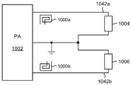
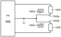
본 개시에 따르면, 단일 도체 전류 센서 (예를 들어, 도 5 에서의 402) 는 차동 전력 증폭기와 함께 사용될 수도 있다. 예를 들어, 차동 전력 증폭기는 무선 전력 송신 회로에 통합되어 송신 코일을 구동할 수도 있다. 도 10a 및 도 10b는 차동 전력 증폭기 구성의 예시적인 실시형태들을 개략적으로 도시한다. 예를 들어, 도 10a 는 부하 (1004, 1006) 에 접속된 차동 전력 증폭기 (1002) 를 도시한다. 전류 센서 (1000a, 1000b) 는 도체 (1042a, 1042b) 를 따라 배치되어 각각의 도체에서 전류의 흐름을 감지할 수도 있다. 전류 센서 (1000a, 1000b) 는 증폭기 (예컨대, 도 4b의 48)에 접속될 수 있는 단일 출력 (예를 들어, 도 4b의 408) 을 생성하기 위해 함께 직렬로 접속될 수도 있다. 도 6을 참조하면, 예를 들어, 전류 센서 (1000a) 의 패드 B 는 전류 센서 (1000b) 의 패드 A 에 접속될 수도 있다. 전류 센서 (1000a) 의 패드 A 및 전류 센서 (1000b) 의 패드 B 는 증폭기 (예를 들어, 48) 에 대한 입력일 수도 있다.According to the present disclosure, a single conductor current sensor (e.g., 402 in FIG. 5) may be used with a differential power amplifier. For example, the differential power amplifier may be integrated into a wireless power transmission circuit to drive the transmit coil. 10A and 10B schematically illustrate exemplary embodiments of a differential power amplifier configuration. For example, FIG. 10A shows a
도 10b 는 전류 센서 (1000a, 1000b) 에 의해 감지되는 도체 (1042a, 1042b) 가 각각의 부하 (1004, 1006) 로부터의 접지 경로를 따라 배치될 수도 있는 구성을 나타낸다. 전류 센서 (1000a, 1000b) 는 직렬로 접속될 수도 있다. 도 10b에 도시된 구성은 도체들 (1042a, 1042b) 에서의 라인 전압이 접지 전위에 가깝기 때문에 일부 응용에서 유리할 수도 있다.Fig. 10B shows a configuration in which
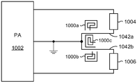
도 10c는, 예를 들어, 차동 증폭기 (1002) 의 도체 (1042a, 1042b) 에서 전류 흐름을 감지하기 위해, 도 9a에 나타낸 것과 같은 이중 도체 단일 전류 센서 (1000c) 의 구성을 나타낸다. 도 10c에 도시된 구성은 도체 (1042a, 1042b) 가 접지 경로를 따라 있는 것으로 도시한다. 그러나, 다른 실시형태에서, 전류 센서 (1000c) 에 의해 감지되는 도체들 (1042a, 1042b) 은 차동 전력 증폭기 (1002) 의 출력에 있을 수도 있다.Fig. 10C shows a configuration of a double-conductor single
또 다른 실시형태에서, 3개 이상의 전류 센서가 사용될 수도 있다. 예를 들어, 도 10b 에 도시된 2개의 단일 도체 전류 센서 (1000a, 1000b) 구성은 도 10c에 도시된 이중 도체 전류 센서 (1000c) 와 직렬 방식으로 결합될 수도 있다. 도 10d는 이러한 구성의 일례를 나타낸다.In yet another embodiment, three or more current sensors may be used. For example, the configuration of the two single
전류 센서는 예를 들어, 전력 제어를 위한 피드백을 제공하기 위해, 무선 전력 회로에서 사용될 수도 있다. 전류 센서는 손실 전력 결정에 특히 유용할 수도 있다. 예를 들어, 전류 센서는 패드 상에서 전력을 소비하는 물체의 존재를 검출하거나 또는 수신기가 수신하고 있는 것에 기초하여 손실된 전력의 양을 결정하기 위하여 송신된 전력의 양을 검출하는데 사용될 수도 있다.The current sensor may be used in a wireless power circuit, for example, to provide feedback for power control. The current sensor may be particularly useful for determining lost power. For example, the current sensor may be used to detect the presence of an object that consumes power on the pad, or to detect the amount of power transmitted to determine the amount of power lost based on what the receiver is receiving.
본 개시에 따른 전류 센서는, 감지되고 있는 전류 흐름과 직접 상호 작용하지 않는다. 따라서, 전류 센서는 전류를 공급하는 전력 증폭기에서 불균형을 발생시키지 않는다. 또한, 본 개시에 따른 전류 센서는 전력 증폭기의 출력으로부터 격리된 출력 전압을 제공할 수 있다.The current sensor according to the present disclosure does not directly interact with the current flow being sensed. Thus, the current sensor does not cause an imbalance in the power amplifier that supplies the current. In addition, the current sensor according to the present disclosure can provide an isolated output voltage from the output of the power amplifier.
본 개시에 따른 전류 센서는 스위칭 회로를 사용하지 않으므로, 전형적으로 스위칭 회로의 사용과 연관된 EMI를 방출하지 않는다.The current sensor according to the present disclosure does not use a switching circuit and thus typically does not emit EMI associated with use of the switching circuit.
본 개시에 따른 전류 센서는 전류와 90 도 위상이 다른 전압 파형을 생성할 수 있으므로, 전류 흐름의 사용 가능한 위상 각 측정을 제공할 수 있다. 또한, 이 파형의 제로 크로싱은 전력 증폭기 출력 전압의 제로 크로싱과 비교되어 위상 각의 정확한 측정을 제공할 수 있다. 이 위상 각은 부하 전력 및 임피던스 측정 양자 모두에 사용될 수 있다.The current sensor according to the present disclosure can generate a voltage waveform that is different from the current by 90 degrees out of phase, thus providing a usable phase angle measurement of the current flow. In addition, the zero crossing of this waveform can be compared to the zero crossing of the power amplifier output voltage to provide an accurate measurement of the phase angle. This phase angle can be used for both the load power and the impedance measurement.
위의 설명은 특정 실시형태들의 양태들이 어떻게 구현될 수도 있는지의 예들과 함께 본 개시의 다양한 실시형태들을 예시한다. 위의 설명들은 유일한 실시형태들인 것으로 여겨져서는 안되고, 다음의 청구항들에 의해 정의되는 특정 실시형태들의 유연성 및 이점들을 예시하기 위해 제시되어 있다. 위의 개시 및 다음의 청구항들에 기초하여, 다른 배열, 실시형태, 구현 및 균등물들이 청구항에 의해 정의되는 본 개시의 범위로부터 벗어남이 없이 채용될 수도 있다.The above description illustrates various embodiments of the present disclosure, together with examples of how aspects of certain embodiments may be implemented. The foregoing description is not to be considered as being unique, but is presented to exemplify the flexibility and advantages of particular embodiments as defined by the following claims. Other arrangements, embodiments, implementations and equivalents may be employed without departing from the scope of the present disclosure as defined by the claims, based on the foregoing disclosure and the following claims.
Claims (30)
도체;
상기 도체에서의 전류의 흐름으로 인해 제 1 위치에서 발생된 제 1 자기장에 커플링하도록 구성된 감지 엘리먼트; 및
상기 감지 엘리먼트에 전기적으로 접속되고 상기 도체에서의 전류의 흐름을 나타내는 신호를 생성하도록 구성된 출력부를 포함하고,
상기 감지 엘리먼트는 상기 제 1 위치와는 상이한 제 2 위치에서 상기 도체에 전기적으로 접속된 부하에 의해 발생된, 상기 제 1 자기장과는 상이한, 제 2 자기장의 자기력선과 평행한 평면에 배향되는, 전류 센서.As a current sensor,
Conductor;
A sensing element configured to couple to a first magnetic field generated at a first location due to the flow of current in the conductor; And
And an output coupled to the sensing element and configured to generate a signal indicative of a current flow in the conductor,
Wherein the sensing element is oriented in a plane parallel to the lines of magnetic force of a second magnetic field, different from the first magnetic field, generated by a load electrically connected to the conductor at a second location different from the first location, sensor.
기판을 더 포함하고, 상기 감지 엘리먼트는 상기 기판 상에 그리고 상기 도체에 인접하게 배치된 도전성 코일을 포함하는, 전류 센서.The method according to claim 1,
Further comprising a substrate, wherein the sensing element comprises a conductive coil disposed on the substrate and adjacent the conductor.
필터 회로를 더 포함하고, 상기 필터 회로는 상기 도전성 코일을 포함하는, 전류 센서.3. The method of claim 2,
Further comprising a filter circuit, wherein the filter circuit comprises the conductive coil.
상기 필터 회로는 대역통과 필터인, 전류 센서.The method of claim 3,
Wherein the filter circuit is a band-pass filter.
상기 기판은 상기 도체를 지니는 인쇄 회로 판 (PCB) 에 수직으로 배치되는, 전류 센서.3. The method of claim 2,
Wherein the substrate is vertically disposed on a printed circuit board (PCB) carrying the conductor.
상기 부하는 무선 전력 전송을 위한 외부 자기장을 발생시키도록 구성된 전력 송신 엘리먼트를 포함하고, 상기 외부 자기장은 상기 제 2 자기장을 구성하는, 전류 센서.The method according to claim 1,
Wherein the load comprises a power transmission element configured to generate an external magnetic field for wireless power transmission and the external magnetic field constitutes the second magnetic field.
상기 감지 엘리먼트는 도전성 코일을 포함하며, 상기 전류 센서는 상기 감지 엘리먼트의 도전성 코일을 포함하는 필터를 더 포함하며, 상기 필터는 상기 전력 송신 엘리먼트의 공진 주파수에 동조되는, 전류 센서.The method according to claim 6,
Wherein the sensing element comprises a conductive coil and wherein the current sensor further comprises a filter comprising a conductive coil of the sensing element, the filter being tuned to a resonant frequency of the power transmitting element.
상기 감지 엘리먼트와 상기 도체 사이에 배치된 용량성 차폐부를 더 포함하며, 상기 용량성 차폐부는 상기 도체에서 발생된 전기장이 상기 감지 엘리먼트에 용량적으로 커플링되는 것을 방지하는데 효과적인, 전류 센서.The method according to claim 1,
Further comprising a capacitive shield disposed between the sensing element and the conductor, wherein the capacitive shield is effective to prevent capacitive coupling of the electric field generated in the conductor to the sensing element.
상기 용량성 차폐부는 상기 감지 엘리먼트와 상기 도체 양자 모두에 인접하게 배치된 전도성 리드를 포함하고, 상기 전도성 리드는 자유 제 1 단부 및 접지 전위에 전기적으로 접속하도록 구성된 제 2 단부를 포함하는, 전류 센서.9. The method of claim 8,
Wherein the capacitive shield comprises a conductive lead disposed adjacent both the sensing element and the conductor and the conductive lead comprises a free end and a second end configured to electrically connect to the ground potential, .
상기 감지 엘리먼트는 제 1 평면 상에 배치된 제 1 도전성 코일 및 상기 제 1 평면으로부터 이격된 적어도 제 2 평면 상에 배치된 적어도 제 2 도전성 코일을 포함하는, 전류 센서.The method according to claim 1,
Wherein the sensing element comprises a first conductive coil disposed on a first plane and at least a second conductive coil disposed on at least a second plane spaced from the first plane.
상기 제 1 도전성 코일 및 상기 도체 양자 모두에 인접하게 배치되도록 구성된 제 1 용량성 차폐부 및 상기 제 2 도전성 코일 및 상기 도체 양자 모두에 인접하게 배치되도록 구성된 적어도 제 2 용량성 차폐부를 더 포함하는, 전류 센서.11. The method of claim 10,
Further comprising a first capacitive shield configured to be disposed adjacent to both the first conductive coil and the conductor and at least a second capacitive shield configured to be disposed adjacent to both the second conductive coil and the conductor, Current sensor.
상기 제 1 도전성 코일은 상기 제 2 도전성 코일과 직렬로 접속되는, 전류 센서.11. The method of claim 10,
And the first conductive coil is connected in series with the second conductive coil.
상기 제 1 도전성 코일은 다층 PCB 의 제 1 층 상에 형성된 제 1 트레이스를 포함하고, 상기 제 2 도전성 코일은 상기 다층 PCB의 제 2 층 상에 형성된 제 2 트레이스를 포함하는, 전류 센서.11. The method of claim 10,
Wherein the first conductive coil comprises a first trace formed on a first layer of a multi-layer PCB and the second conductive coil comprises a second trace formed on a second layer of the multi-layer PCB.
상기 제 1 도전성 코일은 상기 도체의 일 측 상에 배치되고, 상기 제 2 도전성 코일은 상기 도체의 다른 측 상에 배치되는, 전류 센서.11. The method of claim 10,
Wherein the first conductive coil is disposed on one side of the conductor and the second conductive coil is disposed on the other side of the conductor.
필터 회로를 더 포함하고, 상기 필터 회로는 상기 제 1 도전성 코일 및 상기 제 2 도전성 코일 중 어느 하나 또는 양자 모두를 포함하는, 전류 센서.11. The method of claim 10,
Further comprising a filter circuit, wherein the filter circuit includes either or both of the first conductive coil and the second conductive coil.
상기 감지 엘리먼트는 제 1 도전성 코일 및 적어도 제 2 도전성 코일을 포함하며, 제 1 및 제 2 코일들 양자 모두는 동일한 평면 상에 서로 이격되어 있는, 전류 센서.The method according to claim 1,
Wherein the sensing element comprises a first conductive coil and at least a second conductive coil, both of the first and second coils being spaced apart from one another on the same plane.
상기 도체에서의 전류의 흐름으로 인해 상기 도체로부터 비롯되는 제 1 자기장에 자기적 커플링하는 것에 의해 감지된 신호를 발생시키는 단계로서, 상기 자기적 커플링은 상기 도체에 전기적으로 접속된 부하를 통해 상기 전류의 흐름에 의해 발생된 제 2 자기장의 역선과 평행한 평면에 발생하는, 상기 감지된 신호를 발생시키는 단계; 및
상기 감지된 신호로부터 출력 신호를 발생시키는 단계로서, 상기 출력 신호는 상기 도체를 통한 상기 전류의 흐름의 양을 나타내는, 상기 출력 신호를 발생시키는 단계
를 포함하는, 도체에서 전류의 흐름을 감지하는 방법.A method of sensing a current flow in a conductor,
Generating a sensed signal by magnetically coupling to a first magnetic field originating from the conductor due to the flow of current in the conductor, wherein the magnetic coupling is conducted through a load electrically connected to the conductor Generating a sensed signal that occurs in a plane parallel to an inverse of a second magnetic field generated by the flow of current; And
Generating an output signal from the sensed signal, the output signal representing an amount of the current flow through the conductor, generating the output signal
The method comprising the steps of:
상기 제 1 자기장에 자기적 커플링하는 것은 상기 도체에 인접하게 배치되고 상기 제 2 자기장의 역선에 평행한 평면에 정렬된 도전성 재료의 코일에서, 상기 제 1 자기장을 사용하여, 전류를 유도하는 것을 포함하는, 도체에서 전류의 흐름을 감지하는 방법.18. The method of claim 17,
Magnetically coupling to the first magnetic field comprises inducing an electric current using the first magnetic field in a coil of a conductive material disposed adjacent to the conductor and aligned in a plane parallel to an opposite line of the second magnetic field A method for sensing a current flow in a conductor, comprising:
상기 도전성 재료의 코일을 포함하는 필터 회로에 의해 결정된 상기 감지된 신호 내의 주파수 성분들을 감쇠시키기 위해 상기 감지된 신호를 필터링하는 단계를 더 포함하는, 도체에서 전류의 흐름을 감지하는 방법.19. The method of claim 18,
Further comprising filtering the sensed signal to attenuate frequency components in the sensed signal determined by a filter circuit comprising a coil of conductive material. ≪ RTI ID = 0.0 >< / RTI >
상기 부하는 무선 전력 전송을 위한 외부 자기장을 발생시키도록 구성된 전력 송신 엘리먼트를 포함하고, 상기 외부 자기장은 상기 제 2 자기장을 구성하는, 도체에서 전류의 흐름을 감지하는 방법.19. The method of claim 18,
Wherein the load comprises a power transmission element configured to generate an external magnetic field for wireless power transmission and wherein the external magnetic field constitutes the second magnetic field.
상기 도체에서 발생된 전기장으로부터 상기 감지된 신호를, 상기 발생된 출력 신호가 실질적으로 상기 전기장으로부터의 영향이 없도록, 차폐시키는 단계를 더 포함하는, 도체에서 전류의 흐름을 감지하는 방법.18. The method of claim 17,
Further comprising shielding the sensed signal from an electric field generated in the conductor such that the generated output signal is substantially free of influence from the electric field.
상기 제 1 자기장에 자기적으로 커플링하는 것은 상기 제 1 자기장을 상기 도체에 인접하게 배치된 도전성 재료의 제 1 코일에 커플링시키는 것 및 상기 제 1 자기장을 상기 도체에 인접하게 배치된 도전성 재료의 제 2 코일에 커플링시키는 것을 포함하는, 도체에서 전류의 흐름을 감지하는 방법.18. The method of claim 17,
Magnetically coupling said first magnetic field to said first magnetic field comprises coupling said first magnetic field to a first coil of conductive material disposed adjacent to said conductor and coupling said first magnetic field to a conductive material To a second coil of the second coil.
감지된 신호를 발생시키기 위해 상기 도체에서의 전류의 흐름으로 인해 상기 도체로부터 비롯되는 제 1 자기장에 자기적 커플링하는 수단으로서, 상기 제 1 자기장에 자기적 커플링하는 수단은 상기 도체에 전기적으로 접속된 부하를 통해 상기 전류의 흐름에 의해 발생된 제 2 자기장의 역선과 평행한 평면에 정렬되는, 상기 제 1 자기장에 자기적 커플링하는 수단; 및
상기 감지된 신호로부터 출력 신호를 발생시키는 수단
을 포함하는, 도체에서 전류의 흐름을 감지하기 위한 장치.An apparatus for sensing a current flow in a conductor,
Means for magnetically coupling to a first magnetic field originating from said conductor due to the flow of current in said conductor for generating a sensed signal, means for magnetically coupling said first magnetic field to said conductor electrically Means for magnetically coupling to the first magnetic field aligned in a plane parallel to the reverse line of the second magnetic field generated by the flow of current through the connected load; And
Means for generating an output signal from the sensed signal
And for sensing the current flow in the conductor.
상기 감지된 신호를 필터링하는 수단을 더 포함하고, 상기 필터링하는 수단은 제 1 자기장에 자기적 커플링하는 수단을 포함하는, 도체에서 전류의 흐름을 감지하기 위한 장치.24. The method of claim 23,
Means for filtering the sensed signal, the means for filtering including means for magnetically coupling to a first magnetic field.
상기 제 1 자기장에 자기적 커플링하는 수단은 도전성 재료의 코일을 포함하는, 도체에서 전류의 흐름을 감지하기 위한 장치.25. The method of claim 24,
Wherein the means for magnetically coupling to the first magnetic field comprises a coil of conductive material, for sensing the flow of current in the conductor.
상기 필터링하는 수단은 대역통과 필터인, 도체에서 전류의 흐름을 감지하기 위한 장치.25. The method of claim 24,
Wherein the means for filtering is a bandpass filter.
송신 코일;
도체를 통해 상기 송신 코일에 전기적으로 커플링되는 구동기 회로로서, 상기 구동기 회로는 상기 도체를 통해 교류로 상기 송신 코일을 구동하도록 구성된, 상기 구동기 회로; 및
상기 도체에서 전류의 흐름을 감지하도록 구성된 전류 센서로서, 상기 전류 센서는 상기 도체에서 상기 전류의 흐름을 나타내는 신호를 생성하기 위해 상기 도체에서 교류에 의해 발생된 제 1 자기장에 커플링하도록 구성된 감지 코일을 포함하는, 상기 전류 센서
를 포함하고,
상기 송신 코일은 교류에 의해 구동되는 것에 응답하여 상기 수신기 디바이스에 충전 전력을 무선으로 송신하기 위한 제 2 자기장을 발생시키도록 구성되고,
상기 감지 코일은 상기 제 2 자기장의 역선에 평행한 평면에 배향되는, 충전 전력을 무선으로 송신하기 위한 장치.An apparatus for wirelessly transmitting charging power to a receiver device,
Transmitting coil;
A driver circuit electrically coupled to the transmit coil through a conductor, the driver circuit configured to drive the transmit coil in an alternating current through the conductor; And
A current sensor configured to sense a current flow in the conductor, the current sensor comprising a sense coil configured to couple to a first magnetic field generated by an alternating current in the conductor to generate a signal indicative of the flow of current in the conductor, The current sensor
Lt; / RTI >
Wherein the transmit coil is configured to generate a second magnetic field for wirelessly transmitting a charging power to the receiver device in response to being driven by an alternating current,
And wherein the sense coils are oriented in a plane parallel to an inverse of the second magnetic field.
필터 회로를 더 포함하고, 상기 필터 회로는 상기 감지 코일 및 상기 감지 코일에 전기적으로 접속된 저항 및 커패시터를 포함하는, 충전 전력을 무선으로 송신하기 위한 장치.28. The method of claim 27,
Further comprising a filter circuit, wherein the filter circuit comprises a resistor and a capacitor electrically connected to the sense coil and the sense coil.
상기 필터 회로는 대역통과 필터인, 충전 전력을 무선으로 송신하기 위한 장치.29. The method of claim 28,
Wherein the filter circuit is a bandpass filter.
상기 전류 센서는 상기 감지 코일에 인접하게 배치된 용량성 차폐부를 더 포함하며, 상기 용량성 차폐부는 상기 도체에서 생성된 전기장이 상기 감지 코일에 용량적으로 커플링되는 것을 방지하는데 효과적이며, 상기 용량성 차폐부는 상기 도체와 상기 감지 코일 사이에 배치된 제 2 도체를 포함하는, 충전 전력을 무선으로 송신하기 위한 장치.28. The method of claim 27,
Wherein the current sensor further comprises a capacitive shield disposed adjacent to the sense coil and wherein the capacitive shield is effective to prevent capacitive coupling of the electric field generated in the conductor to the sense coil, Wherein the shielding comprises a second conductor disposed between the conductor and the sense coil.
Applications Claiming Priority (4)
| Application Number | Priority Date | Filing Date | Title |
|---|---|---|---|
| US14/618,343 US9958480B2 (en) | 2015-02-10 | 2015-02-10 | Apparatus and method for a current sensor |
| US14/854,443 | 2015-09-15 | ||
| US14/854,443 US20170074908A1 (en) | 2015-02-10 | 2015-09-15 | Apparatus and method for a current sensor |
| PCT/US2016/048332 WO2017048471A1 (en) | 2015-02-10 | 2016-08-24 | Apparatus and method for a current sensor |
Publications (1)
| Publication Number | Publication Date |
|---|---|
| KR20180054686A true KR20180054686A (en) | 2018-05-24 |
Family
ID=55273545
Family Applications (1)
| Application Number | Title | Priority Date | Filing Date |
|---|---|---|---|
| KR1020187010297A KR20180054686A (en) | 2015-02-10 | 2016-08-24 | Apparatus and method for current sensor |
Country Status (6)
| Country | Link |
|---|---|
| US (2) | US9958480B2 (en) |
| EP (2) | EP3256864B1 (en) |
| JP (2) | JP6683719B2 (en) |
| KR (1) | KR20180054686A (en) |
| CN (2) | CN107250812B (en) |
| WO (2) | WO2016130265A1 (en) |
Cited By (1)
| Publication number | Priority date | Publication date | Assignee | Title |
|---|---|---|---|---|
| US11092623B2 (en) | 2018-12-11 | 2021-08-17 | Electronics And Telecommunications Research Institute | Current sensor for measuring alternating electromagnetic wave and a current breaker using the same |
Families Citing this family (29)
| Publication number | Priority date | Publication date | Assignee | Title |
|---|---|---|---|---|
| CN106134032B (en) * | 2014-03-27 | 2018-12-25 | Lg伊诺特有限公司 | Wireless power transmission system with wireless power sending device |
| CN107257167B (en) | 2014-05-27 | 2020-01-21 | 松下知识产权经营株式会社 | Power transmission device and wireless power transmission system |
| US9958480B2 (en) | 2015-02-10 | 2018-05-01 | Qualcomm Incorporated | Apparatus and method for a current sensor |
| US9711272B2 (en) * | 2015-07-09 | 2017-07-18 | Te Connectivity Corporation | Printed circuit for wireless power transfer |
| US10656185B2 (en) * | 2015-07-17 | 2020-05-19 | Mediatek Inc. | Planar differential current pickup for wireless power transmission |
| TWM526343U (en) * | 2016-02-05 | 2016-08-01 | 品法設計國際有限公司 | Wireless temperature maintenance container |
| US10222430B2 (en) * | 2016-03-01 | 2019-03-05 | Mitsumi Electric Co., Ltd. | Sensor device and semiconductor device |
| JP6434456B2 (en) * | 2016-06-23 | 2018-12-05 | 横河電機株式会社 | Isolated voltage probe |
| JP6593274B2 (en) * | 2016-08-03 | 2019-10-23 | 株式会社豊田自動織機 | Multilayer board |
| US11114884B2 (en) * | 2016-09-30 | 2021-09-07 | Intel Corporation | Sensing coil system |
| US10561049B2 (en) * | 2016-10-28 | 2020-02-11 | Integrated Device Technology, Inc. | Interference filter for wireless power transfer systems |
| GB2557272B (en) | 2016-12-02 | 2020-03-18 | Cmr Surgical Ltd | Sensing motor current |
| US10586688B2 (en) * | 2017-01-30 | 2020-03-10 | Lam Research Corporation | Inductive current sensor on printed circuit board |
| JP6853277B2 (en) * | 2017-02-02 | 2021-03-31 | アルプスアルパイン株式会社 | Magnetically balanced current sensor and its manufacturing method |
| KR101937209B1 (en) * | 2017-06-09 | 2019-01-10 | 엘에스산전 주식회사 | Apparatus for sensing current |
| JP2019070563A (en) * | 2017-10-06 | 2019-05-09 | 株式会社デンソー | Current sensor |
| CN107505492B (en) * | 2017-10-17 | 2023-10-13 | 云南电网有限责任公司电力科学研究院 | Device for reducing inductance of current transformer test loop |
| US11046193B2 (en) * | 2018-01-23 | 2021-06-29 | Witricity Corporation | Foreign object detection circuit using current measurement |
| BE1026245B1 (en) * | 2018-05-04 | 2019-12-02 | Phoenix Contact Gmbh & Co | current sensor |
| US10932360B2 (en) | 2018-07-19 | 2021-02-23 | Ut-Battelle, Llc | Flexible sensor technology |
| US11555940B2 (en) | 2018-10-31 | 2023-01-17 | KYOCERA AVX Components (Werne), GmbH | Position sensing apparatus and method |
| EP3891863A4 (en) * | 2018-12-04 | 2022-10-12 | Powermat Technologies Ltd. | Adaptive wireless power transmitter |
| JP2020148640A (en) * | 2019-03-14 | 2020-09-17 | 株式会社東芝 | Current detector |
| US11333686B2 (en) * | 2019-10-21 | 2022-05-17 | Tegam, Inc. | Non-directional in-line suspended PCB power sensing coupler |
| JP7289782B2 (en) * | 2019-12-19 | 2023-06-12 | 株式会社東芝 | current detector |
| US11519941B2 (en) * | 2020-07-27 | 2022-12-06 | Analog Devices International Unlimited Company | Current sensing device having an integrated electrical shield |
| KR102470633B1 (en) * | 2020-12-15 | 2022-11-25 | 한양대학교 산학협력단 | Circuit assembly for Current Detecting |
| US11740264B1 (en) * | 2021-02-05 | 2023-08-29 | Peng Sun | High temperature current sensor for power electronics |
| IT202100021209A1 (en) * | 2021-08-05 | 2023-02-05 | Electroceramica S A | RADIAL CARD, MEASURING DEVICE, EQUIPMENT FOR ELECTROTECHNICAL APPLICATIONS IN THE DOMAIN OF MEDIUM AND HIGH VOLTAGES AND METHOD OF CONSTRUCTION OF THE DEVICE |
Family Cites Families (41)
| Publication number | Priority date | Publication date | Assignee | Title |
|---|---|---|---|---|
| US4887029A (en) | 1988-03-18 | 1989-12-12 | Westinghouse Electric Corp. | Mutual inductance current transducer, method of making and electric energy meter incorporating same |
| US5343143A (en) | 1992-02-11 | 1994-08-30 | Landis & Gyr Metering, Inc. | Shielded current sensing device for a watthour meter |
| DE60002319T2 (en) | 1999-05-25 | 2004-02-12 | Arbeitsgemeinschaft Prof. Hugel Agph | ELECTRIC CURRENT SENSOR |
| US6348800B1 (en) | 1999-09-28 | 2002-02-19 | Rockwell Automation Technologies, Inc. | Multi-phase ground fault current sensor system |
| JP2001264364A (en) | 2000-03-14 | 2001-09-26 | Matsushita Electric Ind Co Ltd | Optical current transformer |
| US6501364B1 (en) * | 2001-06-15 | 2002-12-31 | City University Of Hong Kong | Planar printed-circuit-board transformers with effective electromagnetic interference (EMI) shielding |
| WO2006090769A1 (en) | 2005-02-23 | 2006-08-31 | Asahi Kasei Emd Corporation | Current measuring instrument |
| JP5116667B2 (en) | 2005-06-10 | 2013-01-09 | バード テクノロジーズ グループ インク. | System and method for analyzing power flow in a semiconductor plasma generation system |
| JP4916807B2 (en) | 2006-01-30 | 2012-04-18 | 株式会社ダイヘン | Voltage detection printed circuit board and voltage detector using the same |
| JP2008211951A (en) | 2007-02-28 | 2008-09-11 | Brother Ind Ltd | Non contact type charger and non contact type charging apparatus |
| JP4965402B2 (en) | 2007-09-27 | 2012-07-04 | パナソニック株式会社 | Current sensor |
| FR2932568B1 (en) * | 2008-06-11 | 2010-06-11 | Schneider Electric Ind Sas | CURRENT MEASURING DEVICE AND PROCESSING UNIT COMPRISING SUCH A DEVICE |
| EP2136216B1 (en) | 2008-06-19 | 2012-01-11 | ABB Technology AG | A combined electrical measurement device |
| JP5143765B2 (en) | 2009-02-16 | 2013-02-13 | 株式会社東海理化電機製作所 | Current sensor |
| US20110172552A1 (en) | 2010-01-12 | 2011-07-14 | Vanderbilt University | Acoustic sleep apnea monitor |
| JP5562054B2 (en) * | 2010-01-29 | 2014-07-30 | 富士通株式会社 | Table tap and power measurement system |
| EP2643704B1 (en) | 2010-11-26 | 2018-01-24 | The National Microelectronics Applications Centre | An ac current or voltage sensor |
| US20120146165A1 (en) * | 2010-12-09 | 2012-06-14 | Udo Ausserlechner | Magnetic field current sensors |
| US8669677B2 (en) | 2010-12-28 | 2014-03-11 | Tdk Corporation | Wireless power feeder, wireless power receiver, and wireless power transmission system |
| CN103415776B (en) * | 2011-03-02 | 2015-06-03 | 阿尔卑斯绿色器件株式会社 | Current sensor |
| GB201110825D0 (en) | 2011-06-27 | 2011-08-10 | Sentec Ltd | Sensors |
| CN102866279A (en) | 2011-07-04 | 2013-01-09 | 新科实业有限公司 | Current sensor device |
| US8872611B2 (en) | 2011-08-18 | 2014-10-28 | General Electric Company | Rogowski coil assemblies and methods for providing the same |
| JP5533826B2 (en) * | 2011-09-19 | 2014-06-25 | 株式会社デンソー | Current sensor and current sensor assembly structure |
| US9354033B2 (en) | 2011-11-18 | 2016-05-31 | Fluke Corporation | Smart electromagnetic sensor array |
| WO2013098975A1 (en) * | 2011-12-27 | 2013-07-04 | 富士通株式会社 | Wireless power supply apparatus, wireless power supply system, and wireless power supply method |
| WO2013172109A1 (en) | 2012-05-16 | 2013-11-21 | アルプス・グリーンデバイス株式会社 | Current sensor |
| US9291649B2 (en) | 2012-08-16 | 2016-03-22 | Mks Instruments, Inc. | On the enhancements of planar based RF sensor technology |
| US9275791B2 (en) | 2012-08-31 | 2016-03-01 | Qualcomm Incorporated | Systems and methods for decoupling multiple wireless charging transmitters |
| WO2014063159A2 (en) | 2012-10-19 | 2014-04-24 | Witricity Corporation | Foreign object detection in wireless energy transfer systems |
| US9921243B2 (en) | 2012-12-17 | 2018-03-20 | Covidien Lp | System and method for voltage and current sensing |
| EP2953235B1 (en) | 2013-01-29 | 2018-09-12 | Fujitsu Limited | Wireless power transfer system, power receiver, and wireless power transfer method |
| US10192678B2 (en) * | 2013-02-21 | 2019-01-29 | Ferrarispower Co., Ltd | Current transformer system with sensor CT and generator CT separately arranged in parallel in electric power line, and integrated system for controlling same in wireless communications network |
| US9379556B2 (en) * | 2013-03-14 | 2016-06-28 | Cooper Technologies Company | Systems and methods for energy harvesting and current and voltage measurements |
| JP5814976B2 (en) | 2013-05-15 | 2015-11-17 | 三菱電機株式会社 | Current measuring device |
| DE102013106100A1 (en) | 2013-06-12 | 2014-12-31 | Phoenix Contact Gmbh & Co. Kg | Stom sensor arrangement with measuring coils |
| JP6286157B2 (en) | 2013-09-05 | 2018-02-28 | ルネサスエレクトロニクス株式会社 | Sensor device |
| US9322806B2 (en) * | 2013-10-25 | 2016-04-26 | General Electric Company | Eddy current sensor with linear drive conductor |
| CZ2013822A3 (en) | 2013-10-25 | 2015-02-04 | České Vysoké Učení Technické V Praze Univerzitní Centrum Energeticky Efektivních Budov | Contactless magnetic position sensor of magnetic or electrically conducting objects |
| JP6201896B2 (en) * | 2014-05-30 | 2017-09-27 | 株式会社Ihi | Power transmission device and non-contact power feeding system |
| US9958480B2 (en) | 2015-02-10 | 2018-05-01 | Qualcomm Incorporated | Apparatus and method for a current sensor |
-
2015
- 2015-02-10 US US14/618,343 patent/US9958480B2/en active Active
- 2015-09-15 US US14/854,443 patent/US20170074908A1/en not_active Abandoned
-
2016
- 2016-01-13 WO PCT/US2016/013231 patent/WO2016130265A1/en active Application Filing
- 2016-01-13 EP EP16702467.8A patent/EP3256864B1/en active Active
- 2016-01-13 CN CN201680009327.2A patent/CN107250812B/en active Active
- 2016-01-13 JP JP2017541641A patent/JP6683719B2/en not_active Expired - Fee Related
- 2016-08-24 WO PCT/US2016/048332 patent/WO2017048471A1/en active Application Filing
- 2016-08-24 CN CN201680053447.2A patent/CN108027392A/en active Pending
- 2016-08-24 EP EP16766114.9A patent/EP3350605A1/en not_active Withdrawn
- 2016-08-24 JP JP2018513372A patent/JP2018534543A/en active Pending
- 2016-08-24 KR KR1020187010297A patent/KR20180054686A/en unknown
Cited By (1)
| Publication number | Priority date | Publication date | Assignee | Title |
|---|---|---|---|---|
| US11092623B2 (en) | 2018-12-11 | 2021-08-17 | Electronics And Telecommunications Research Institute | Current sensor for measuring alternating electromagnetic wave and a current breaker using the same |
Also Published As
| Publication number | Publication date |
|---|---|
| CN107250812B (en) | 2019-12-10 |
| EP3350605A1 (en) | 2018-07-25 |
| JP2018534543A (en) | 2018-11-22 |
| EP3256864A1 (en) | 2017-12-20 |
| US20160231364A1 (en) | 2016-08-11 |
| JP2018512564A (en) | 2018-05-17 |
| US9958480B2 (en) | 2018-05-01 |
| US20170074908A1 (en) | 2017-03-16 |
| JP6683719B2 (en) | 2020-04-22 |
| EP3256864B1 (en) | 2019-01-02 |
| CN107250812A (en) | 2017-10-13 |
| WO2017048471A1 (en) | 2017-03-23 |
| CN108027392A (en) | 2018-05-11 |
| WO2016130265A1 (en) | 2016-08-18 |
Similar Documents
| Publication | Publication Date | Title |
|---|---|---|
| KR20180054686A (en) | Apparatus and method for current sensor | |
| US9917479B2 (en) | Wireless energy transfer for mobile device applications | |
| EP3685198B1 (en) | Device and method for foreign object detection in wireless energy transfer | |
| US9562955B2 (en) | Methods and apparatus for magnetic field strength measurement | |
| EP3840176B1 (en) | Apparatus for inductive power transfer | |
| JP2016019305A (en) | Power transmission device and power reception device | |
| US11921251B2 (en) | Position sensing apparatus and method | |
| CN107148710B (en) | Wireless power transfer using stacked resonators | |
| CN107370249B (en) | Power transmitting device and non-contact power supply system | |
| US20170222481A1 (en) | Wireless power transfer in an electronic device having a tuned metallic body | |
| JP4848799B2 (en) | Circuit board having junction current or voltage detection and adjustment function, and electronic device mounted with the same | |
| JP2013253967A (en) | Multipolar magnetic field sensor for metal surface, sensor system and manufacturing method of multipolar magnetic field sensor for metal surface | |
| US20180017599A1 (en) | Current detection element, transmission device, and electric power transmission system | |
| JP2014059198A (en) | Sensing system |