KR20180025901A - Ultra-thin barrier laminates and devices - Google Patents
Ultra-thin barrier laminates and devices Download PDFInfo
- Publication number
- KR20180025901A KR20180025901A KR1020187002111A KR20187002111A KR20180025901A KR 20180025901 A KR20180025901 A KR 20180025901A KR 1020187002111 A KR1020187002111 A KR 1020187002111A KR 20187002111 A KR20187002111 A KR 20187002111A KR 20180025901 A KR20180025901 A KR 20180025901A
- Authority
- KR
- South Korea
- Prior art keywords
- layer
- thermoplastic polymer
- barrier
- major surface
- skin layer
- Prior art date
Links
- 230000004888 barrier function Effects 0.000 title claims abstract description 151
- 239000010410 layer Substances 0.000 claims abstract description 332
- 229920001169 thermoplastic Polymers 0.000 claims abstract description 93
- 239000011241 protective layer Substances 0.000 claims abstract description 59
- 229920000642 polymer Polymers 0.000 claims description 96
- 239000000203 mixture Substances 0.000 claims description 80
- 239000000853 adhesive Substances 0.000 claims description 33
- 230000001070 adhesive effect Effects 0.000 claims description 33
- 230000005693 optoelectronics Effects 0.000 claims description 31
- 238000000034 method Methods 0.000 claims description 29
- 229920001577 copolymer Polymers 0.000 claims description 25
- 229920000139 polyethylene terephthalate Polymers 0.000 claims description 23
- 239000005020 polyethylene terephthalate Substances 0.000 claims description 23
- 238000000576 coating method Methods 0.000 claims description 18
- QQONPFPTGQHPMA-UHFFFAOYSA-N propylene Natural products CC=C QQONPFPTGQHPMA-UHFFFAOYSA-N 0.000 claims description 18
- 239000012790 adhesive layer Substances 0.000 claims description 14
- 239000011159 matrix material Substances 0.000 claims description 14
- 239000011248 coating agent Substances 0.000 claims description 13
- 229920000728 polyester Polymers 0.000 claims description 13
- 230000032798 delamination Effects 0.000 claims description 10
- -1 polyethylene terephthalate Polymers 0.000 claims description 10
- 239000013047 polymeric layer Substances 0.000 claims description 10
- 229920006132 styrene block copolymer Polymers 0.000 claims description 9
- XLYOFNOQVPJJNP-UHFFFAOYSA-N water Chemical compound O XLYOFNOQVPJJNP-UHFFFAOYSA-N 0.000 claims description 8
- 150000001336 alkenes Chemical class 0.000 claims description 7
- 229920001400 block copolymer Polymers 0.000 claims description 7
- 229920006037 cross link polymer Polymers 0.000 claims description 7
- JRZJOMJEPLMPRA-UHFFFAOYSA-N olefin Natural products CCCCCCCC=C JRZJOMJEPLMPRA-UHFFFAOYSA-N 0.000 claims description 7
- 239000002096 quantum dot Substances 0.000 claims description 7
- 229920000058 polyacrylate Polymers 0.000 claims description 6
- 239000004416 thermosoftening plastic Substances 0.000 claims description 6
- 239000004952 Polyamide Substances 0.000 claims description 5
- 239000004793 Polystyrene Substances 0.000 claims description 5
- 229920006213 ethylene-alphaolefin copolymer Polymers 0.000 claims description 5
- 229920002647 polyamide Polymers 0.000 claims description 5
- 239000004417 polycarbonate Substances 0.000 claims description 5
- 229920000515 polycarbonate Polymers 0.000 claims description 5
- 229920000098 polyolefin Polymers 0.000 claims description 5
- 229920002223 polystyrene Polymers 0.000 claims description 5
- 230000005540 biological transmission Effects 0.000 claims description 4
- 238000006243 chemical reaction Methods 0.000 claims description 4
- 239000011112 polyethylene naphthalate Substances 0.000 claims description 4
- 229920002635 polyurethane Polymers 0.000 claims description 4
- 239000004814 polyurethane Substances 0.000 claims description 4
- 239000011229 interlayer Substances 0.000 claims description 3
- 239000002245 particle Substances 0.000 claims description 2
- 238000004519 manufacturing process Methods 0.000 abstract description 4
- 239000011247 coating layer Substances 0.000 abstract 1
- 239000011575 calcium Substances 0.000 description 23
- 239000000758 substrate Substances 0.000 description 23
- OYPRJOBELJOOCE-UHFFFAOYSA-N Calcium Chemical compound [Ca] OYPRJOBELJOOCE-UHFFFAOYSA-N 0.000 description 20
- 229910052791 calcium Inorganic materials 0.000 description 20
- 239000000463 material Substances 0.000 description 18
- 239000011521 glass Substances 0.000 description 13
- 230000000052 comparative effect Effects 0.000 description 10
- 238000000231 atomic layer deposition Methods 0.000 description 9
- QVGXLLKOCUKJST-UHFFFAOYSA-N atomic oxygen Chemical compound [O] QVGXLLKOCUKJST-UHFFFAOYSA-N 0.000 description 9
- 239000001301 oxygen Substances 0.000 description 9
- 229910052760 oxygen Inorganic materials 0.000 description 9
- NIXOWILDQLNWCW-UHFFFAOYSA-M Acrylate Chemical compound [O-]C(=O)C=C NIXOWILDQLNWCW-UHFFFAOYSA-M 0.000 description 8
- 238000000151 deposition Methods 0.000 description 8
- 229910052751 metal Inorganic materials 0.000 description 7
- 239000002184 metal Substances 0.000 description 7
- 238000012360 testing method Methods 0.000 description 7
- 229920005601 base polymer Polymers 0.000 description 6
- 230000007797 corrosion Effects 0.000 description 6
- 238000005260 corrosion Methods 0.000 description 6
- 230000008021 deposition Effects 0.000 description 6
- 239000000178 monomer Substances 0.000 description 6
- 239000002243 precursor Substances 0.000 description 6
- 238000004544 sputter deposition Methods 0.000 description 6
- 239000004820 Pressure-sensitive adhesive Substances 0.000 description 5
- IJGRMHOSHXDMSA-UHFFFAOYSA-N Atomic nitrogen Chemical compound N#N IJGRMHOSHXDMSA-UHFFFAOYSA-N 0.000 description 4
- CURLTUGMZLYLDI-UHFFFAOYSA-N Carbon dioxide Chemical compound O=C=O CURLTUGMZLYLDI-UHFFFAOYSA-N 0.000 description 4
- 229920001634 Copolyester Polymers 0.000 description 4
- VYPSYNLAJGMNEJ-UHFFFAOYSA-N Silicium dioxide Chemical compound O=[Si]=O VYPSYNLAJGMNEJ-UHFFFAOYSA-N 0.000 description 4
- PPBRXRYQALVLMV-UHFFFAOYSA-N Styrene Chemical compound C=CC1=CC=CC=C1 PPBRXRYQALVLMV-UHFFFAOYSA-N 0.000 description 4
- 230000000875 corresponding effect Effects 0.000 description 4
- 238000010894 electron beam technology Methods 0.000 description 4
- 238000012986 modification Methods 0.000 description 4
- 230000004048 modification Effects 0.000 description 4
- 230000008569 process Effects 0.000 description 4
- 230000001681 protective effect Effects 0.000 description 4
- GWEVSGVZZGPLCZ-UHFFFAOYSA-N Titan oxide Chemical compound O=[Ti]=O GWEVSGVZZGPLCZ-UHFFFAOYSA-N 0.000 description 3
- YAIQCYZCSGLAAN-UHFFFAOYSA-N [Si+4].[O-2].[Al+3] Chemical compound [Si+4].[O-2].[Al+3] YAIQCYZCSGLAAN-UHFFFAOYSA-N 0.000 description 3
- 230000008901 benefit Effects 0.000 description 3
- 238000005229 chemical vapour deposition Methods 0.000 description 3
- 230000009977 dual effect Effects 0.000 description 3
- 238000005516 engineering process Methods 0.000 description 3
- 238000001755 magnetron sputter deposition Methods 0.000 description 3
- 238000005259 measurement Methods 0.000 description 3
- 229910044991 metal oxide Inorganic materials 0.000 description 3
- 150000004706 metal oxides Chemical class 0.000 description 3
- 230000003287 optical effect Effects 0.000 description 3
- 230000035699 permeability Effects 0.000 description 3
- 229920005989 resin Polymers 0.000 description 3
- 239000011347 resin Substances 0.000 description 3
- XKRFYHLGVUSROY-UHFFFAOYSA-N Argon Chemical compound [Ar] XKRFYHLGVUSROY-UHFFFAOYSA-N 0.000 description 2
- 229920002633 Kraton (polymer) Polymers 0.000 description 2
- CERQOIWHTDAKMF-UHFFFAOYSA-M Methacrylate Chemical compound CC(=C)C([O-])=O CERQOIWHTDAKMF-UHFFFAOYSA-M 0.000 description 2
- 229920002367 Polyisobutene Polymers 0.000 description 2
- 229910052782 aluminium Inorganic materials 0.000 description 2
- 239000001569 carbon dioxide Substances 0.000 description 2
- 229910002092 carbon dioxide Inorganic materials 0.000 description 2
- 150000001875 compounds Chemical class 0.000 description 2
- 238000010276 construction Methods 0.000 description 2
- 238000004132 cross linking Methods 0.000 description 2
- 238000001514 detection method Methods 0.000 description 2
- 238000005566 electron beam evaporation Methods 0.000 description 2
- 238000001704 evaporation Methods 0.000 description 2
- 230000008020 evaporation Effects 0.000 description 2
- 238000001125 extrusion Methods 0.000 description 2
- 229920001519 homopolymer Polymers 0.000 description 2
- JCXJVPUVTGWSNB-UHFFFAOYSA-N nitrogen dioxide Inorganic materials O=[N]=O JCXJVPUVTGWSNB-UHFFFAOYSA-N 0.000 description 2
- TWNQGVIAIRXVLR-UHFFFAOYSA-N oxo(oxoalumanyloxy)alumane Chemical compound O=[Al]O[Al]=O TWNQGVIAIRXVLR-UHFFFAOYSA-N 0.000 description 2
- 238000000623 plasma-assisted chemical vapour deposition Methods 0.000 description 2
- 229920006254 polymer film Polymers 0.000 description 2
- 238000012545 processing Methods 0.000 description 2
- 229910052710 silicon Inorganic materials 0.000 description 2
- 229910052814 silicon oxide Inorganic materials 0.000 description 2
- 238000010998 test method Methods 0.000 description 2
- 229910052580 B4C Inorganic materials 0.000 description 1
- 229910052582 BN Inorganic materials 0.000 description 1
- ZOXJGFHDIHLPTG-UHFFFAOYSA-N Boron Chemical compound [B] ZOXJGFHDIHLPTG-UHFFFAOYSA-N 0.000 description 1
- PZNSFCLAULLKQX-UHFFFAOYSA-N Boron nitride Chemical compound N#B PZNSFCLAULLKQX-UHFFFAOYSA-N 0.000 description 1
- 229920000089 Cyclic olefin copolymer Polymers 0.000 description 1
- 239000004713 Cyclic olefin copolymer Substances 0.000 description 1
- 239000004593 Epoxy Substances 0.000 description 1
- 244000043261 Hevea brasiliensis Species 0.000 description 1
- VQTUBCCKSQIDNK-UHFFFAOYSA-N Isobutene Chemical group CC(C)=C VQTUBCCKSQIDNK-UHFFFAOYSA-N 0.000 description 1
- 229920001410 Microfiber Polymers 0.000 description 1
- 239000004698 Polyethylene Substances 0.000 description 1
- 239000004642 Polyimide Substances 0.000 description 1
- 239000004743 Polypropylene Substances 0.000 description 1
- 229920001328 Polyvinylidene chloride Polymers 0.000 description 1
- 229910052581 Si3N4 Inorganic materials 0.000 description 1
- XUIMIQQOPSSXEZ-UHFFFAOYSA-N Silicon Chemical compound [Si] XUIMIQQOPSSXEZ-UHFFFAOYSA-N 0.000 description 1
- 239000004433 Thermoplastic polyurethane Substances 0.000 description 1
- 238000003848 UV Light-Curing Methods 0.000 description 1
- SQWOCMZNVYUDSE-UHFFFAOYSA-N [Zr+4].[Zr+4].[Zr+4].[O-]B([O-])[O-].[O-]B([O-])[O-].[O-]B([O-])[O-].[O-]B([O-])[O-] Chemical compound [Zr+4].[Zr+4].[Zr+4].[O-]B([O-])[O-].[O-]B([O-])[O-].[O-]B([O-])[O-].[O-]B([O-])[O-] SQWOCMZNVYUDSE-UHFFFAOYSA-N 0.000 description 1
- VEBCLRKUSAGCDF-UHFFFAOYSA-N ac1mi23b Chemical compound C1C2C3C(COC(=O)C=C)CCC3C1C(COC(=O)C=C)C2 VEBCLRKUSAGCDF-UHFFFAOYSA-N 0.000 description 1
- NIXOWILDQLNWCW-UHFFFAOYSA-N acrylic acid group Chemical group C(C=C)(=O)O NIXOWILDQLNWCW-UHFFFAOYSA-N 0.000 description 1
- 229920006243 acrylic copolymer Polymers 0.000 description 1
- XECAHXYUAAWDEL-UHFFFAOYSA-N acrylonitrile butadiene styrene Chemical compound C=CC=C.C=CC#N.C=CC1=CC=CC=C1 XECAHXYUAAWDEL-UHFFFAOYSA-N 0.000 description 1
- 229920000122 acrylonitrile butadiene styrene Polymers 0.000 description 1
- 239000004676 acrylonitrile butadiene styrene Substances 0.000 description 1
- 230000001464 adherent effect Effects 0.000 description 1
- 230000032683 aging Effects 0.000 description 1
- XAGFODPZIPBFFR-UHFFFAOYSA-N aluminium Chemical compound [Al] XAGFODPZIPBFFR-UHFFFAOYSA-N 0.000 description 1
- PNEYBMLMFCGWSK-UHFFFAOYSA-N aluminium oxide Inorganic materials [O-2].[O-2].[O-2].[Al+3].[Al+3] PNEYBMLMFCGWSK-UHFFFAOYSA-N 0.000 description 1
- 229910052786 argon Inorganic materials 0.000 description 1
- 230000000712 assembly Effects 0.000 description 1
- 238000000429 assembly Methods 0.000 description 1
- 229910052796 boron Inorganic materials 0.000 description 1
- INAHAJYZKVIDIZ-UHFFFAOYSA-N boron carbide Chemical compound B12B3B4C32B41 INAHAJYZKVIDIZ-UHFFFAOYSA-N 0.000 description 1
- 238000007596 consolidation process Methods 0.000 description 1
- PMHQVHHXPFUNSP-UHFFFAOYSA-M copper(1+);methylsulfanylmethane;bromide Chemical compound Br[Cu].CSC PMHQVHHXPFUNSP-UHFFFAOYSA-M 0.000 description 1
- 230000002596 correlated effect Effects 0.000 description 1
- 230000007423 decrease Effects 0.000 description 1
- 230000007547 defect Effects 0.000 description 1
- 238000005115 demineralization Methods 0.000 description 1
- 230000002328 demineralizing effect Effects 0.000 description 1
- 238000005137 deposition process Methods 0.000 description 1
- 238000001227 electron beam curing Methods 0.000 description 1
- 229920002313 fluoropolymer Polymers 0.000 description 1
- 239000004811 fluoropolymer Substances 0.000 description 1
- 239000007789 gas Substances 0.000 description 1
- 238000011065 in-situ storage Methods 0.000 description 1
- 229910003437 indium oxide Inorganic materials 0.000 description 1
- PJXISJQVUVHSOJ-UHFFFAOYSA-N indium(iii) oxide Chemical compound [O-2].[O-2].[O-2].[In+3].[In+3] PJXISJQVUVHSOJ-UHFFFAOYSA-N 0.000 description 1
- AMGQUBHHOARCQH-UHFFFAOYSA-N indium;oxotin Chemical compound [In].[Sn]=O AMGQUBHHOARCQH-UHFFFAOYSA-N 0.000 description 1
- 239000004615 ingredient Substances 0.000 description 1
- 229910010272 inorganic material Inorganic materials 0.000 description 1
- 239000011147 inorganic material Substances 0.000 description 1
- 238000010030 laminating Methods 0.000 description 1
- 238000003475 lamination Methods 0.000 description 1
- 239000007788 liquid Substances 0.000 description 1
- 150000001247 metal acetylides Chemical class 0.000 description 1
- 150000002739 metals Chemical class 0.000 description 1
- 239000003658 microfiber Substances 0.000 description 1
- XCOASYLMDUQBHW-UHFFFAOYSA-N n-(3-trimethoxysilylpropyl)butan-1-amine Chemical compound CCCCNCCC[Si](OC)(OC)OC XCOASYLMDUQBHW-UHFFFAOYSA-N 0.000 description 1
- 229920003052 natural elastomer Polymers 0.000 description 1
- 229920001194 natural rubber Polymers 0.000 description 1
- 229910000484 niobium oxide Inorganic materials 0.000 description 1
- URLJKFSTXLNXLG-UHFFFAOYSA-N niobium(5+);oxygen(2-) Chemical compound [O-2].[O-2].[O-2].[O-2].[O-2].[Nb+5].[Nb+5] URLJKFSTXLNXLG-UHFFFAOYSA-N 0.000 description 1
- 150000004767 nitrides Chemical class 0.000 description 1
- 229910052757 nitrogen Inorganic materials 0.000 description 1
- VIKNJXKGJWUCNN-XGXHKTLJSA-N norethisterone Chemical compound O=C1CC[C@@H]2[C@H]3CC[C@](C)([C@](CC4)(O)C#C)[C@@H]4[C@@H]3CCC2=C1 VIKNJXKGJWUCNN-XGXHKTLJSA-N 0.000 description 1
- 201000007909 oculocutaneous albinism Diseases 0.000 description 1
- BPUBBGLMJRNUCC-UHFFFAOYSA-N oxygen(2-);tantalum(5+) Chemical compound [O-2].[O-2].[O-2].[O-2].[O-2].[Ta+5].[Ta+5] BPUBBGLMJRNUCC-UHFFFAOYSA-N 0.000 description 1
- 230000002093 peripheral effect Effects 0.000 description 1
- 239000003348 petrochemical agent Substances 0.000 description 1
- 239000004014 plasticizer Substances 0.000 description 1
- 238000007747 plating Methods 0.000 description 1
- 229920000573 polyethylene Polymers 0.000 description 1
- 229920001721 polyimide Polymers 0.000 description 1
- 229920001155 polypropylene Polymers 0.000 description 1
- 229920002689 polyvinyl acetate Polymers 0.000 description 1
- 239000011118 polyvinyl acetate Substances 0.000 description 1
- 229920000915 polyvinyl chloride Polymers 0.000 description 1
- 239000004800 polyvinyl chloride Substances 0.000 description 1
- 229920001289 polyvinyl ether Polymers 0.000 description 1
- 239000005033 polyvinylidene chloride Substances 0.000 description 1
- 230000002028 premature Effects 0.000 description 1
- SCUZVMOVTVSBLE-UHFFFAOYSA-N prop-2-enenitrile;styrene Chemical compound C=CC#N.C=CC1=CC=CC=C1 SCUZVMOVTVSBLE-UHFFFAOYSA-N 0.000 description 1
- 230000005855 radiation Effects 0.000 description 1
- 238000005546 reactive sputtering Methods 0.000 description 1
- 230000004044 response Effects 0.000 description 1
- 238000007753 roll-to-roll coating process Methods 0.000 description 1
- 239000010703 silicon Substances 0.000 description 1
- HBMJWWWQQXIZIP-UHFFFAOYSA-N silicon carbide Chemical compound [Si+]#[C-] HBMJWWWQQXIZIP-UHFFFAOYSA-N 0.000 description 1
- 229910010271 silicon carbide Inorganic materials 0.000 description 1
- 239000000377 silicon dioxide Substances 0.000 description 1
- HQVNEWCFYHHQES-UHFFFAOYSA-N silicon nitride Chemical compound N12[Si]34N5[Si]62N3[Si]51N64 HQVNEWCFYHHQES-UHFFFAOYSA-N 0.000 description 1
- 241000894007 species Species 0.000 description 1
- 238000005477 sputtering target Methods 0.000 description 1
- 229920000638 styrene acrylonitrile Polymers 0.000 description 1
- 229920001935 styrene-ethylene-butadiene-styrene Polymers 0.000 description 1
- 239000000126 substance Substances 0.000 description 1
- 229920003051 synthetic elastomer Polymers 0.000 description 1
- 239000005061 synthetic rubber Substances 0.000 description 1
- 229910001936 tantalum oxide Inorganic materials 0.000 description 1
- 229920001897 terpolymer Polymers 0.000 description 1
- 238000002207 thermal evaporation Methods 0.000 description 1
- 229920002803 thermoplastic polyurethane Polymers 0.000 description 1
- XOLBLPGZBRYERU-UHFFFAOYSA-N tin dioxide Chemical compound O=[Sn]=O XOLBLPGZBRYERU-UHFFFAOYSA-N 0.000 description 1
- 229910001887 tin oxide Inorganic materials 0.000 description 1
- OGIDPMRJRNCKJF-UHFFFAOYSA-N titanium oxide Inorganic materials [Ti]=O OGIDPMRJRNCKJF-UHFFFAOYSA-N 0.000 description 1
- MTPVUVINMAGMJL-UHFFFAOYSA-N trimethyl(1,1,2,2,2-pentafluoroethyl)silane Chemical compound C[Si](C)(C)C(F)(F)C(F)(F)F MTPVUVINMAGMJL-UHFFFAOYSA-N 0.000 description 1
- JLTRXTDYQLMHGR-UHFFFAOYSA-N trimethylaluminium Chemical compound C[Al](C)C JLTRXTDYQLMHGR-UHFFFAOYSA-N 0.000 description 1
- UONOETXJSWQNOL-UHFFFAOYSA-N tungsten carbide Chemical compound [W+]#[C-] UONOETXJSWQNOL-UHFFFAOYSA-N 0.000 description 1
- 238000009834 vaporization Methods 0.000 description 1
- 230000008016 vaporization Effects 0.000 description 1
- 239000011800 void material Substances 0.000 description 1
- 238000004804 winding Methods 0.000 description 1
Images


Classifications
-
- B—PERFORMING OPERATIONS; TRANSPORTING
- B32—LAYERED PRODUCTS
- B32B—LAYERED PRODUCTS, i.e. PRODUCTS BUILT-UP OF STRATA OF FLAT OR NON-FLAT, e.g. CELLULAR OR HONEYCOMB, FORM
- B32B7/00—Layered products characterised by the relation between layers; Layered products characterised by the relative orientation of features between layers, or by the relative values of a measurable parameter between layers, i.e. products comprising layers having different physical, chemical or physicochemical properties; Layered products characterised by the interconnection of layers
- B32B7/04—Interconnection of layers
- B32B7/06—Interconnection of layers permitting easy separation
-
- B—PERFORMING OPERATIONS; TRANSPORTING
- B32—LAYERED PRODUCTS
- B32B—LAYERED PRODUCTS, i.e. PRODUCTS BUILT-UP OF STRATA OF FLAT OR NON-FLAT, e.g. CELLULAR OR HONEYCOMB, FORM
- B32B27/00—Layered products comprising a layer of synthetic resin
- B32B27/06—Layered products comprising a layer of synthetic resin as the main or only constituent of a layer, which is next to another layer of the same or of a different material
- B32B27/08—Layered products comprising a layer of synthetic resin as the main or only constituent of a layer, which is next to another layer of the same or of a different material of synthetic resin
-
- B—PERFORMING OPERATIONS; TRANSPORTING
- B32—LAYERED PRODUCTS
- B32B—LAYERED PRODUCTS, i.e. PRODUCTS BUILT-UP OF STRATA OF FLAT OR NON-FLAT, e.g. CELLULAR OR HONEYCOMB, FORM
- B32B27/00—Layered products comprising a layer of synthetic resin
- B32B27/36—Layered products comprising a layer of synthetic resin comprising polyesters
-
- H01L51/448—
-
- H01L51/5253—
-
- H—ELECTRICITY
- H10—SEMICONDUCTOR DEVICES; ELECTRIC SOLID-STATE DEVICES NOT OTHERWISE PROVIDED FOR
- H10K—ORGANIC ELECTRIC SOLID-STATE DEVICES
- H10K30/00—Organic devices sensitive to infrared radiation, light, electromagnetic radiation of shorter wavelength or corpuscular radiation
- H10K30/80—Constructional details
- H10K30/88—Passivation; Containers; Encapsulations
-
- H—ELECTRICITY
- H10—SEMICONDUCTOR DEVICES; ELECTRIC SOLID-STATE DEVICES NOT OTHERWISE PROVIDED FOR
- H10K—ORGANIC ELECTRIC SOLID-STATE DEVICES
- H10K50/00—Organic light-emitting devices
- H10K50/80—Constructional details
- H10K50/84—Passivation; Containers; Encapsulations
- H10K50/844—Encapsulations
-
- H—ELECTRICITY
- H10—SEMICONDUCTOR DEVICES; ELECTRIC SOLID-STATE DEVICES NOT OTHERWISE PROVIDED FOR
- H10K—ORGANIC ELECTRIC SOLID-STATE DEVICES
- H10K59/00—Integrated devices, or assemblies of multiple devices, comprising at least one organic light-emitting element covered by group H10K50/00
- H10K59/10—OLED displays
- H10K59/12—Active-matrix OLED [AMOLED] displays
- H10K59/1201—Manufacture or treatment
-
- B—PERFORMING OPERATIONS; TRANSPORTING
- B32—LAYERED PRODUCTS
- B32B—LAYERED PRODUCTS, i.e. PRODUCTS BUILT-UP OF STRATA OF FLAT OR NON-FLAT, e.g. CELLULAR OR HONEYCOMB, FORM
- B32B2307/00—Properties of the layers or laminate
- B32B2307/70—Other properties
- B32B2307/724—Permeability to gases, adsorption
- B32B2307/7242—Non-permeable
- B32B2307/7246—Water vapor barrier
-
- B—PERFORMING OPERATIONS; TRANSPORTING
- B32—LAYERED PRODUCTS
- B32B—LAYERED PRODUCTS, i.e. PRODUCTS BUILT-UP OF STRATA OF FLAT OR NON-FLAT, e.g. CELLULAR OR HONEYCOMB, FORM
- B32B2457/00—Electrical equipment
- B32B2457/20—Displays, e.g. liquid crystal displays, plasma displays
- B32B2457/206—Organic displays, e.g. OLED
-
- H—ELECTRICITY
- H10—SEMICONDUCTOR DEVICES; ELECTRIC SOLID-STATE DEVICES NOT OTHERWISE PROVIDED FOR
- H10K—ORGANIC ELECTRIC SOLID-STATE DEVICES
- H10K71/00—Manufacture or treatment specially adapted for the organic devices covered by this subclass
- H10K71/80—Manufacture or treatment specially adapted for the organic devices covered by this subclass using temporary substrates
Abstract
초박형 배리어 라미네이트를 포함하는 배리어 조립체 및 배리어 조립체의 제조 방법이 제공된다. 배리어 조립체는 서로 반대편에 있는 제1 및 제2 주 표면을 갖는 열가소성 중합체 스킨 층, 및 열가소성 중합체 스킨 층의 제1 주 표면 상에 코팅되어 약 0.5 밀 (약 12.7 마이크로미터) 이하의 두께를 갖는 일체형 보호 층을 형성하는 배리어 스택을 포함한다. 제거가능한 캐리어 필름은 열가소성 중합체 스킨 층의 제2 주 표면에 이형가능하게 부착된 주 표면을 갖는다. 일부 경우에, 캐리어 필름의 제거는 초박형 배리어 라미네이트를 생성한다.A barrier assembly comprising an ultra-thin barrier laminate and a method of making the barrier assembly are provided. Barrier assembly comprises a thermoplastic polymer skin layer having first and second major surfaces opposite to each other and an integral polymeric coating layer coated on the first major surface of the thermoplastic polymer skin layer and having a thickness of about 0.5 millimeters (about 12.7 micrometers) And a barrier stack forming a protective layer. The removable carrier film has a major surface releasably attached to the second major surface of the thermoplastic polymer skin layer. In some cases, removal of the carrier film produces an ultra-thin barrier laminate.
Description
본 발명은 초박형 배리어 라미네이트(ultrathin barrier laminate) 및 이의 제조 및 사용 방법에 관한 것이다.The present invention relates to an ultrathin barrier laminate and a method of making and using the same.
유기 발광 다이오드 (organic light emitting diode; OLED), 유기 및 무기 광기전 장치 (PV), 양자점 (QD) 장치와 같은 다수의 전자 장치가 산소 및/또는 물 침입(ingress)으로부터의 보호를 필요로 한다. 배리어 코팅 또는 필름이, 예를 들어 가요성 전자 장치의 분야에서, 전자 장치를 보호하기 위해 개발되어 왔다. 이용가능한 배리어 코팅 또는 필름은 일반적으로 기재(substrate) 및 기재 위에 놓인 배리어 필름을 포함하는 연속 층들의 스택(stack)이며, 여기서 전체로서의 기재 및 배리어 필름은 전자 장치에 대한 보호를 제공할 수 있다.Many electronic devices such as organic light emitting diodes (OLEDs), organic and inorganic photovoltaic devices (PV), and quantum dot (QD) devices require protection from oxygen and / or water ingress . Barrier coatings or films have been developed to protect electronic devices, for example in the field of flexible electronic devices. Available barrier coatings or films are generally a stack of continuous layers comprising a substrate and a barrier film overlying the substrate, wherein the substrate as a whole and the barrier film can provide protection to the electronic device.
배리어 코팅 또는 필름의 두께를 감소시킬 필요가 있다. 그러나, 기재 두께가 감소함에 따라 얇은 연속 필름의 웨브 취급 및 변환은 더 어려워질 수 있다. 예를 들어, 롤-투-롤(roll-to-roll) 코팅 공정에서 웨브 장력을 유지하고 웨브의 열 부하 및 팽창을 관리하는 것은 얇은 기재의 주름 형성 및 결합을 야기할 수 있다. 본 발명은 초박형 배리어 라미네이트를 포함하는 배리어 조립체 및 이의 제조 방법을 제공하며, 이는 상기 과제를 극복할 수 있게 한다.It is necessary to reduce the thickness of the barrier coating or film. However, as the substrate thickness decreases, web handling and conversion of thin continuous films can become more difficult. For example, maintaining web tension in a roll-to-roll coating process and managing the heat load and expansion of the web can cause creasing and bonding of the thin substrate. The present invention provides a barrier assembly comprising an ultra-thin barrier laminate and a method of manufacturing the same, which overcomes the above-mentioned problems.
간단히 말해, 일 태양에서, 본 발명은 서로 반대편에 있는 제1 및 제2 주 표면을 갖는 열가소성 중합체 스킨 층, 및 스킨 층의 제1 주 표면 상에 코팅된 배리어 스택을 포함하는 물품을 기술한다. 열가소성 중합체 스킨 층 및 배리어 스택은 일체형 보호 층을 형성하고, 일체형 보호 층은 두께가 약 0.5 밀 (12.7 마이크로미터) 이하이다. 제거가능한 캐리어 필름은 열가소성 중합체 스킨 층의 제2 주 표면에 이형가능하게 부착된 주 표면을 갖는다. 제거가능한 캐리어 필름은 일체형 보호 층을 지지하도록 구성된다.Briefly, in one aspect, the present invention describes an article comprising a thermoplastic polymer skin layer having first and second major surfaces opposite to each other, and a barrier stack coated on a first major surface of the skin layer. The thermoplastic polymer skin layer and the barrier stack form an integral protective layer, and the integral protective layer has a thickness of about 0.5 mils (12.7 micrometers) or less. The removable carrier film has a major surface releasably attached to the second major surface of the thermoplastic polymer skin layer. The removable carrier film is configured to support the integral protective layer.
다른 태양에서, 본 발명은 주 표면을 갖는 광전자 장치를 기술한다. 열가소성 중합체 스킨 층은 서로 반대편에 있는 제1 및 제2 주 표면을 갖고, 배리어 스택은 열가소성 중합체 스킨 층의 제1 주 표면 상에 코팅된다. 열가소성 중합체 스킨 층 및 배리어 스택은 일체형 보호 층을 형성한다. 일체형 보호 층은 두께가 약 0.5 밀 (12.7 마이크로미터) 이하이다. 일체형 보호 층의 배리어 스택은 광전자 장치의 주 표면에 부착된다.In another aspect, the present invention describes an optoelectronic device having a major surface. The thermoplastic polymer skin layer has first and second major surfaces opposite to each other, and the barrier stack is coated on the first major surface of the thermoplastic polymer skin layer. The thermoplastic polymer skin layer and the barrier stack form an integral protective layer. The integral protective layer has a thickness of about 0.5 mils (12.7 micrometers) or less. The barrier stack of the integral protective layer is attached to the main surface of the optoelectronic device.
다른 태양에서, 본 발명은 주 표면을 갖는 제거가능한 캐리어 필름을 제공하는 단계, 및 제거가능한 캐리어 필름의 주 표면 상에 배치되는 열가소성 중합체 스킨 층을 제공하는 단계를 포함하는 방법을 기술한다. 열가소성 중합체 스킨 층은 서로 반대편에 있는 제1 및 제2 주 표면을 갖고, 열가소성 중합체 스킨 층의 제2 주 표면은 제거가능한 캐리어 필름의 주 표면에 이형가능하게 부착된다. 배리어 스택은 스킨 층의 제1 주 표면 상에 코팅된다. 열가소성 중합체 스킨 층 및 배리어 스택은 약 0.5 밀 (12.7 마이크로미터) 이하의 두께를 갖는 일체형 보호 층을 형성한다.In another aspect, the present invention describes a method comprising providing a removable carrier film having a major surface, and providing a thermoplastic polymer skin layer disposed on a major surface of the removable carrier film. The thermoplastic polymer skin layer has first and second major surfaces opposite to each other and the second major surface of the thermoplastic polymer skin layer is releasably attached to the major surface of the removable carrier film. The barrier stack is coated on the first major surface of the skin layer. The thermoplastic polymer skin layer and the barrier stack form an integral protective layer having a thickness of about 0.5 mils (12.7 micrometers) or less.
본 발명의 예시적인 실시 형태에서 다양한 예상치 못한 결과 및 이점이 얻어진다. 본 발명의 예시적인 실시 형태의 한 가지 그러한 이점은, 최종 사용 시에 제거되어 초박형 라미네이트 배리어 구조를 생성할 수 있는 하나 이상의 스트리핑 가능하거나 제거가능한 층을 배리어 조립체가 갖는 한편, 동시에 배리어 조립체의 더 두꺼운 다층 구조가 롤-투-롤 공정에서의 웨브 취급 및 코팅을 가능하게 할 수 있다는 점이다.Various unexpected results and advantages are obtained in the exemplary embodiment of the present invention. One such advantage of the exemplary embodiments of the present invention is that while the barrier assembly has one or more strippable or removable layers that can be removed during final use to create an ultra-thin laminate barrier structure, Layer structure can enable web handling and coating in a roll-to-roll process.
본 발명의 예시적인 실시 형태의 다양한 태양 및 이점이 요약되었다. 상기 발명의 내용은 본 발명의 각각의 예시된 실시 형태 또는 이 예시적인 특정 실시 형태의 모든 구현 형태를 설명하기 위한 것은 아니다. 하기의 도면 및 상세한 설명은 본 명세서에 개시된 원리를 이용하는 소정의 바람직한 실시 형태를 더 상세하게 예시한다.Various aspects and advantages of the exemplary embodiments of the present invention have been summarized. The above description is not intended to illustrate each illustrated embodiment of the invention or every implementation of this exemplary specific embodiment. The following drawings and detailed description illustrate certain preferred embodiments in further detail using the principles disclosed herein.
본 발명은 첨부 도면과 함께 본 발명의 다양한 실시 형태에 대한 하기의 상세한 설명을 고찰함으로써 더욱 완전히 이해될 수 있다.
도 1은 일 실시 형태에 따른 다층 필름의 개략적인 측면도이다.
도 2는 일 실시 형태에 따른 다층 필름의 개략적인 측면도이다.
도 3a는 일 실시 형태에 따른 배리어 조립체의 개략적인 측면도이다.
도 3b는 도 3a의 배리어 조립체의 확대된 부분이다.
도 4a는 일 실시 형태에 따른, 도 3a의 배리어 조립체를 전자 장치에 적용하는 것에 의한 전자 장치의 개략적인 측면도이다.
도 4b는 캐리어 필름을 제거하여 전자 장치 상에 일체형 보호 층을 생성한, 도 4a의 전자 장치의 개략적인 측면도이다.
도 4c는 제2 일체형 보호 층을 일체형 보호 층에 적용하는 것에 의한 도 4b의 전자 장치의 개략적인 측면도이다.
도 5는 일 실시 형태에 따른, 도 3a의 배리어 조립체를 전자 장치에 직접 적용하는 것에 의한 광전자 장치의 개략적인 측면도이다.
도면에서, 유사한 도면 부호는 유사한 요소를 지시한다. 축척에 맞게 작성되지 않을 수 있는 전술된 도면이 본 발명의 다양한 실시 형태를 개시하고 있지만, 발명을 실시하기 위한 구체적인 내용에 언급된 바와 같이, 다른 실시 형태가 또한 고려된다. 모든 경우에, 본 발명은 현재 개시되는 발명을 명백한 제한으로서가 아니라 예시적인 실시 형태의 표현으로서 기술한다. 본 발명의 범주 및 사상에 속하는 많은 다른 변형 및 실시 형태가 당업자에 의해 고안될 수 있음을 이해하여야 한다.BRIEF DESCRIPTION OF THE DRAWINGS The invention can be more fully understood by considering the following detailed description of various embodiments of the invention in conjunction with the accompanying drawings.
1 is a schematic side view of a multilayer film according to one embodiment.
2 is a schematic side view of a multilayer film according to one embodiment.
3A is a schematic side view of a barrier assembly in accordance with one embodiment.
Figure 3b is an enlarged view of the barrier assembly of Figure 3a.
4A is a schematic side view of an electronic device by applying the barrier assembly of FIG. 3A to an electronic device, in accordance with one embodiment.
Figure 4b is a schematic side view of the electronic device of Figure 4a, which removes the carrier film to create an integral protective layer on the electronic device.
4C is a schematic side view of the electronic device of FIG. 4B by applying the second integral protective layer to the integral protective layer.
5 is a schematic side view of an optoelectronic device by applying the barrier assembly of FIG. 3A directly to an electronic device, in accordance with one embodiment.
In the drawings, like reference numerals designate like elements. While the foregoing drawings, which may not be drawn to scale, disclose various embodiments of the invention, other embodiments are also contemplated, as set forth in the Detailed Description for carrying out the invention. In all cases, the present invention describes the presently disclosed invention as an expression of an exemplary embodiment, not as obvious limitations. It should be understood that many other modifications and embodiments belonging to the scope and spirit of the invention may be devised by those skilled in the art.
정의된 용어에 대한 하기의 용어 해설의 경우, 청구범위 또는 본 명세서의 어딘가 다른 곳에서 상이한 정의가 제공되지 않는 한, 이들의 정의가 전체 출원에 적용되어야 한다.In the following glossary of terms for defined terms, their definitions shall apply to the entire application unless a different definition is provided in the claims or elsewhere in this specification.
용어 해설Glossary of terms
대부분은 잘 알려져 있지만 어떤 설명을 필요로 할 수 있는 소정의 용어가 본 명세서 및 청구범위 전체에 걸쳐 사용된다. 하기를 이해하여야 한다:Certain terminology is used throughout this specification and claims, many of which are well known, but which may require some explanation. It should be understood that:
용어 "균질한"은 거시적인 규모에서 관찰할 때 물질의 단일상만을 나타냄을 의미한다.The term "homogeneous" means only a single phase of the material when viewed on a macroscopic scale.
용어 "(공)중합체" 또는 "(공)중합체들"은 단일중합체 및 공중합체뿐만 아니라, 예를 들어 공압출에 의해, 또는 예를 들어 에스테르 교환반응을 포함하는 반응에 의해 혼화성 블렌드로 형성될 수 있는 단일중합체 또는 공중합체를 포함한다. 용어 "공중합체"는 랜덤, 블록 및 별형(star)(예를 들어, 수지상(dendritic)) 공중합체를 포함한다.The term "(co) polymer" or "(co) polymers" refers to a polymer that is formed by homopolymers and copolymers, as well as by co-extrusion or by reaction involving, for example, ≪ / RTI > homopolymers or copolymers. The term "copolymer" includes random, block and star (e.g., dendritic) copolymers.
특정 층과 관련하여 용어 "서로 접한"(adjoining)은, 2개의 층이 서로의 옆에서 (즉, 서로 인접해서) 직접 접촉해 있거나 또는 서로 근접하지만 직접 접촉해 있지는 않은 (즉, 층들 사이에 개재하는 하나 이상의 추가적 층이 있는) 위치에서, 다른 층과 연결되거나 또는 다른 층에 부착된 것을 의미한다.The term "adjoining " with respect to a particular layer means that two layers are in direct contact with each other (i.e., adjacent to each other) or close to each other but not in direct contact (i.e., ≪ / RTI > with one or more additional layers to form a layer), or attached to another layer.
개시된 코팅된 물품에서 다양한 요소들의 위치에 대해 "상부에"(atop), "상에"(on), "위에"(over), "덮는"(covering), "최상부에"(uppermost), "아래에 놓인"(underlying) 등과 같은 배향 용어를 사용함으로써, 수평으로 배치되고 위쪽으로 향해 있는 기재에 대한 요소의 상대적 위치를 지칭한다. 그러나, 달리 지시되지 않는 한, 기재 또는 물품이 제조 동안에 또는 제조 후에 공간 내에서 임의의 특정 배향을 가져야만 하는 것으로 의도되지 않는다.The terms "atop", "on", "over", "covering", "uppermost", " Refers to the relative position of the element relative to the horizontally disposed and upwardly facing substrate by using orientation terms such as "underlying " and the like. However, unless otherwise indicated, the substrate or article is not intended to have any particular orientation in space during or after manufacture.
본 발명의 물품의 기재 또는 다른 요소와 관련하여 층의 위치를 설명하는 데에 용어 "오버코팅된"을 사용함으로써, 기재 또는 다른 요소의 위에 있지만 그러한 기재 또는 다른 요소에 반드시 근접(contiguous)해 있지는 않은 층을 지칭한다.By using the term "overcoated" in describing the position of a layer in relation to the description of the article of the present invention or other elements, it is to be understood that the present invention is not contiguous to a substrate or other element, Quot;
층의 위치를 다른 층들에 대해 기술하기 위해 용어 "~에 의해 분리된"을 사용함으로써, 2개의 다른 층들 사이에 위치되지만 어느 쪽의 층에도 반드시 근접하거나 인접해 있지 않는 층을 지칭한다.Refers to a layer located between two different layers, but not necessarily adjacent or adjacent to either layer, by using the term "separated by " to describe the location of the layer with respect to the other layers.
수치 값 또는 형상과 관련하여 용어 "약" 또는 "대략"은 수치 값 또는 특성 또는 특징의 +/-5%를 의미하지만, 정확한 수치 값을 명확히 포함한다. 예를 들어, "약" 1 Pa-sec의 점도는 0.95 내지 1.05 Pa-sec의 점도를 말하지만, 정확하게 1 Pa-sec의 점도를 또한 명확히 포함한다. 유사하게, "실질적으로 정사각형"인 주연부는, 각각의 측면 에지가 임의의 다른 측면 에지의 길이의 95% 내지 105%인 길이를 갖는 4개의 측면 에지를 갖는 기하학적 형상을 설명하려는 것이지만, 각각의 측면 에지가 정확하게 동일한 길이를 갖는 기하학적 형상을 또한 포함한다.The term " about "or" approximately " in relation to a numerical value or shape implies +/- 5% of a numerical value or characteristic or characteristic, but clearly includes an exact numerical value. For example, a viscosity of "about" 1 Pa-sec refers to a viscosity of 0.95 to 1.05 Pa-sec, but also clearly includes a viscosity of exactly 1 Pa-sec. Similarly, the "substantially square" peripheral is intended to describe a geometric shape having four side edges with each side edge having a length that is 95% to 105% of the length of any other side edge, The edges also include geometric shapes that have exactly the same length.
특성 또는 특징과 관련하여 용어 "실질적으로"는 특성 또는 특징이, 그러한 특성 또는 특징과 정반대의 것이 나타나는 것보다 더 큰 정도로 나타난다는 것을 의미한다. 예를 들어, "실질적으로" 투명한 기재는 투과시키지 못하는 (예를 들어, 흡수하고 반사하는) 것보다 더 많은 방사선(예를 들어, 가시광)을 투과시키는 기재를 말한다. 따라서, 기재 표면 상에 입사하는 가시광의 50% 초과를 투과시키는 기재는 실질적으로 투명하지만, 그 표면 상에 입사하는 가시광의 50% 이하를 투과시키는 기재는 실질적으로 투명한 것이 아니다.The term "substantially" in the context of a feature or characteristic means that the feature or feature appears to a greater extent than what appears to be the opposite of that feature or feature. For example, a "substantially" transparent substrate refers to a substrate that transmits more radiation (e.g., visible light) than it does not transmit (e.g., absorb and reflect). Therefore, the base material through which more than 50% of the visible light incident on the base material surface is substantially transparent, but the base material through which not more than 50% of the visible light incident on the surface is not substantially transparent.
본 명세서 및 첨부된 실시 형태에서 사용되는 바와 같이, 단수 형태("a", "an", 및 "the")는 그 내용이 명백히 달리 지시하지 않는다면 복수의 지시대상을 포함한다. 따라서, 예를 들어, "화합물"을 함유하는 미세 섬유에 대한 언급은 둘 이상의 화합물의 혼합물을 포함한다. 본 명세서 및 첨부된 실시 형태에서 사용되는 바와 같이, 용어 "또는"은 그 내용이 명백히 달리 지시되지 않는 한 "및/또는"을 포함하는 의미로 일반적으로 사용된다.As used in this specification and the appended claims, the singular forms "a," "an," and "the" include plural referents unless the context clearly dictates otherwise. Thus, for example, reference to a microfiber containing a "compound" includes a mixture of two or more compounds. As used in this specification and the appended embodiments, the term "or" is generally used to mean "and / or ", unless the context clearly indicates otherwise.
본 명세서에 사용되는 바와 같이, 종점(endpoint)에 의한 수치 범위의 언급은 그 범위 내에 포함되는 모든 수를 포함한다(예를 들어, 1 내지 5는 1, 1.5, 2, 2.75, 3, 3.8, 4 및 5를 포함한다).As used herein, reference to a numerical range by an endpoint includes all numbers contained within that range (e.g., 1 to 5 are 1, 1.5, 2, 2.75, 3, 3.8, 4 and 5).
달리 지시되지 않는 한, 본 명세서 및 실시 형태에 사용되는, 성분의 양, 특성의 측정치 등을 표현하는 모든 수는 모든 경우에 용어 "약"에 의해 수식되는 것으로 이해되어야 한다. 따라서, 반대로 지시되지 않는 한, 전술한 명세서 및 첨부된 실시 형태의 목록에 기재된 수치 파라미터는 본 발명의 교시 내용을 이용하여 당업자가 얻고자 하는 원하는 특성에 따라 달라질 수 있다. 최소한으로, 그리고 청구된 실시 형태의 범주에 대한 균등론의 적용을 제한하려는 시도로서가 아니라, 각각의 수치 파라미터는 보고된 유효숫자의 개수의 관점에서 그리고 보통의 반올림 기법을 적용함으로써 적어도 해석되어야 한다.Unless otherwise indicated, all numbers expressing quantities of ingredients, measurements of properties, etc. used in the specification and embodiments are to be understood as being modified in all instances by the term "about ". Accordingly, unless indicated to the contrary, the numerical parameters set forth in the foregoing specification and in the accompanying list of embodiments may vary depending upon the desired properties sought to be obtained by those skilled in the art using the teachings of the present invention. At the very least, and not as an attempt to limit the application of the doctrine of equivalents to the scope of the claimed embodiments, each numerical parameter should at least be construed in light of the number of reported significant digits and by applying ordinary rounding techniques.
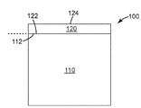
도 1은 일 실시 형태에 따른, 다층 필름(100)의 개략적인 단면도를 예시한다. 다층 필름(100)은 제거가능한 캐리어 필름(110), 및 제거가능한 캐리어 필름(110) 상에 배치된 열가소성 중합체 스킨 층(120)을 포함한다. 제거가능한 캐리어 필름(110)은 열가소성 중합체 스킨 층(120)의 주 표면(122)으로부터 분리가능한 주 표면(112)을 가져서, 열가소성 중합체 스킨 층(120) 및 제거가능한 캐리어 필름(110)은 연속 시트 형태로 서로로부터 탈층(delamination)될 수 있다. 탈층은, 이 경우에 접촉 표면(122, 112)인 탈층 표면(도 1의 점선 참조)을 따라 우선적으로 일어날 수 있다. 일부 실시 형태에서, 열가소성 중합체 스킨 층(120)은 폴리에스테르, 폴리올레핀, 폴리아크릴레이트, 폴리아미드, 폴리카르보네이트, 폴리우레탄, 및 폴리스티렌으로 이루어진 군으로부터 선택되는 하나 이상의 열가소성 중합체일 수 있거나 그를 포함할 수 있다. 일부 실시 형태에서, 열가소성 중합체는, 예를 들어, 폴리에틸렌 테레프탈레이트 (PET), 폴리스티렌, 아크릴로니트릴 부타디엔 스티렌, 폴리비닐 클로라이드, 폴리비닐리덴 클로라이드, 폴리카르보네이트, 폴리아크릴레이트, 열가소성 폴리우레탄, 폴리비닐 아세테이트, 폴리아미드, 폴리이미드, 폴리에틸렌 나프탈레이트 (PEN), 스티렌 아크릴로니트릴, 실리콘-폴리옥사미드 중합체, 플루오로중합체, 환형 올레핀 공중합체 등 중 하나 이상을 포함할 수 있다.Figure 1 illustrates a schematic cross-sectional view of a
도 2는 예시적인 열가소성 중합체 스킨 층(120)이 배치된 예시적인 제거가능한 캐리어 필름(110)을 포함하는 예시적인 다층 필름(200)을 예시한다. 제거가능한 캐리어 필름(110)은 제거가능한 캐리어 필름(110)의 전부 또는 일부를 형성할 수 있는 스택(220)을 형성하도록 함께 적층된 개개의 중합체 층들을 포함한다. 도시된 실시 형태에서, 스택(220)은 두 가지 유형의 중합체 층, 즉 중합체 층 A 및 중합체 층 B를 포함하며, 이들은 각각 상이한 중합체 조성물 A 및 중합체 조성물 B로 구성되는 것으로 가정된다. 제거가능한 캐리어 필름(110) 및 열가소성 중합체 스킨 층(120)은 다른 적합한 구조 및/또는 조성을 가질 수 있는 것으로 이해되어야 한다.FIG. 2 illustrates an
도 2의 실시 형태에서, 열가소성 중합체 스킨 층(120)은 또한 조성물 A를 포함하는 중합체 층 A이고, 열가소성 중합체 스킨 층(120)에 인접한 스택(220)의 최전방 층은 조성물 B를 포함하는 중합체 층 B이다. 열가소성 중합체 스킨 층(120) 및 스택(220)을 포함하는 다층 필름(200)은 A/B/A/B/A의 대칭적 5층 구조를 형성한다. 다층 필름(200)은 다른 개수의 층, 예를 들어, A/B/A의 3층 구조, 또는 더 많은 교번하는 A 및 B 층을 포함할 수 있는 것으로 이해되어야 한다. 제거가능한 캐리어 필름(110) 및 열가소성 중합체 스킨 층(120)이 서로로부터 탈층될 수 있기만 하다면, 중합체 조성물 A 및 중합체 조성물 B는 다른 순서로 배열될 수 있는 것으로 또한 이해되어야 한다.In the embodiment of Figure 2 the thermoplastic
일부 실시 형태에서, 중합체 조성물 A 또는 중합체 조성물 B는 폴리에스테르계 재료를 포함할 수 있다. 일부 실시 형태에서, 폴리에스테르계 및 비-폴리에스테르계 재료 조합물이 스택(220) 내의 층 B, 또는 층 A에 각각 적절하게 포함될 수 있다. 일부 실시 형태에서, 중합체 조성물 A는, 예를 들어, 반결정질 폴리에스테르일 수 있다. 일부 실시 형태에서, 중합체 조성물 B는, 예를 들어, 프로필렌 공중합체와 스티렌성 블록 공중합체의 블렌드, 또는 프로필렌 공중합체와 에틸렌 알파 올레핀 공중합체의 블렌드, 또는 프로필렌 공중합체와 올레핀 블록 공중합체의 블렌드일 수 있다.In some embodiments, polymer composition A or polymer composition B may comprise a polyester-based material. In some embodiments, a polyester-based and non-polyester-based material combination may suitably be included in layer B, or layer A, in
일부 실시 형태에서, 인접한 A 층과 B 층 사이의 부착성(attachment)은 실질적으로 동일할 수 있다. 즉, 실질적으로 동일한 양의 박리력을 가하여 인접한 A 층과 B 층을 탈층시킬 수 있다. 스택(220)의 일부 또는 전부가, 인접한 A 층과 B 층 사이의 각각의 계면에 상응하는 임의의 원하는 탈층 표면을 따라 탈층될 수 있다. 제거가능한 캐리어 필름(110)은 층마다(layer-by-layer) 열가소성 중합체 스킨 층(120)으로부터 제거될 수 있다.In some embodiments, the attachment between adjacent A and B layers may be substantially the same. That is, it is possible to remove adjacent layers A and B by applying substantially the same amount of peeling force. Some or all of the
일부 실시 형태에서, 스택(220)은 인접한 층(120)(예를 들어, 중합체 층 A)과 스택(220)의 최전방 층 B 사이의 탈층 계면(도 2의 점선 참조)을 따라 우선적으로 탈층될 수 있다. 전체로서의 캐리어 필름(110)이 탈층 계면을 따라 열가소성 중합체 스킨 층(120)으로부터 제거될 수 있다.In some embodiments, the
일부 실시 형태에서, 스택(220)은 인접한 중합체 층 A와 중합체 층 B에 의해 개재된(sandwiched) 하나 이상의 중합체 층 C를 포함하여, 예를 들어, 최전방 층 B가 열가소성 중합체 스킨 층(120)에 제거가능하게 부착된 B/C/A/C/B/C/A의 구조를 형성할 수 있다. 중합체 층 C는 인접한 층 A와 층 B 사이의 중간층이며, 층 A와 층 B 사이의 부착성을 향상시킬 수 있는 조성물 C를 갖는다. 중합체 조성물 B는 프로필렌 공중합체와 스티렌성 블록 공중합체의 블렌드일 수 있거나 그를 포함할 수 있고, 중합체 조성물 C는 코폴리에스테르와 올레핀의 혼화성 블렌드일 수 있거나 그를 포함할 수 있다. 중합체 조성물 B는 프로필렌 공중합체와 스티렌성 블록 공중합체의 블렌드일 수 있거나 그를 포함할 수 있고, 중합체 조성물 C는 무정형 코폴리에스테르일 수 있거나 그를 포함할 수 있고, 중합체 조성물 A는 반결정질 폴리에스테르일 수 있거나 그를 포함할 수 있다. 중합체 조성물 B는 중합체 조성물 C와 (적어도 부분적으로) 혼화성일 수 있는 반면, 중합체 조성물 C는 중합체 조성물 A와 (적어도 부분적으로) 혼화성이고, 중합체 조성물 B는 중합체 조성물 A와 혼화성이 아니다.In some embodiments, the
일부 실시 형태에서, 캐리어 필름(110)의 최전방 층 (예를 들어, 중합체 층 B)은 최전방 층 아래에 놓인 내부 층에 대한 부착성보다 열가소성 중합체 스킨 층(120)에 대한 부착성이 실질적으로 더 약할 수 있다. 스택(220)의 최전방 중합체 층에 대한 열가소성 중합체 스킨 층(120)의 부착성은, 예를 들어, 2 내지 100 그램/인치의 범위의 박리력에 의해 특징지어질 수 있다. 스택(220)의 최전방 중합체 층에 대한 열가소성 중합체 스킨 층(120)의 부착성은 제1 박리력에 의해 특징지어질 수 있다. 최전방 중합체 층 아래에 놓인 내부 중합체 층에 대한 스택(220)의 최전방 중합체 층의 부착성은 제2 박리력에 의해 특징지어질 수 있다. 일부 실시 형태에서, 상기에 논의된 B/C/A 구성을 갖는 스택(220)의 경우, 제2 박리력은 제1 박리력의 2배 이상, 또는 3배 이상일 수 있다.In some embodiments, the foremost layer (e. G., Polymer layer B) of the
일부 실시 형태에서, 중합체 조성물 B는 프로필렌 공중합체와 스티렌성 블록 공중합체의 혼화성 블렌드, 또는 프로필렌 공중합체와 에틸렌 알파 올레핀 공중합체의 혼화성 블렌드, 또는 프로필렌 공중합체와 올레핀 블록 공중합체의 혼화성 블렌드일 수 있다. 중합체 조성물 B가 프로필렌 공중합체와 스티렌성 블록 공중합체의 혼화성 블렌드인 경우에, 중합체 조성물 C는 코폴리에스테르와 올레핀의 비혼화성 블렌드일 수 있거나, 또는 중합체 조성물 C는 무정형 코폴리에스테르일 수 있고 중합체 조성물 A는 반결정질 폴리에스테르일 수 있다.In some embodiments, polymer composition B is a miscible blend of a propylene copolymer and a styrenic block copolymer, or a miscible blend of a propylene copolymer and an ethylene alpha olefin copolymer, or a miscible blend of a propylene copolymer and an olefin block copolymer Blend < / RTI > In the case where polymer composition B is a miscible blend of a propylene copolymer and a styrenic block copolymer, polymer composition C may be an incompatible blend of copolyester and olefin, or polymer composition C may be an amorphous copolyester Polymer composition A may be a semi-crystalline polyester.
바람직하게는, 중합체 조성물 A, 중합체 조성물 B, 및 중합체 조성물 C 중의 어느 것도 감압 접착제 (PSA), 또는 다른 유형의 접착제가 아니다. 게다가, 다층 필름(200)의 중합체 조성물 A, 중합체 조성물 B, 및/또는 중합체 조성물 C는 바람직하게는 서로 공압출가능하여, 전체 층 스택(220) 및 그 상의 열가소성 중합체 스킨 층(120)은, 상이한 작업에서 제조된 다음 추후에 접착제로 함께 라미네이팅되기보다는 단일 작업에서 공압출될 수 있다. 그러한 공압출된 중합체 필름 구성이 미국 특허 출원 공개 제2014/0065397호 (존슨(Johnson) 등)에 기술되어 있으며, 이는 전술한 개시 내용과 상충되지 않는 한 참고로 포함된다. 제거가능한 캐리어 필름(110)은 하나씩 박리될 수 있는 둘 이상의 스택(220)을 포함할 수 있는 것으로 이해되어야 한다.Preferably, none of polymer composition A, polymer composition B, and polymer composition C is a pressure sensitive adhesive (PSA), or other type of adhesive. In addition, the polymer composition A, polymer composition B, and / or polymer composition C of the
일부 실시 형태에서, 제거가능한 캐리어 필름(110) 및 열가소성 중합체 스킨 층(120)이 간단히 떼어지지 않도록 보장하기 위하여, 캐리어 필름(110)의 최전방 층 (예를 들어, 도 2의 스택(220)의 위쪽 층(B))에 대한 열가소성 중합체 스킨 층(120)의 부착성은 0 초과의 박리력에 의해 특징지어지며, 예를 들어, 박리력은 바람직하게는 1 그램/인치 이상, 또는 2 그램/인치 이상이다. g/in로 약칭되는 그램/인치(또는 그램/인치 폭)의 박리력 단위는 때때로 gli로 약칭되는 직선 인치당 그램(gram per linear inch)으로 지칭된다. 1 g/in는 0.3860886 N/m과 같다.In some embodiments, the topmost layer of the carrier film 110 (e.g., the top surface of the
일부 실시 형태에서, 선택적인 프리마스크(premask)가 캐리어 필름(110)에 부착될 수 있으며, 예를 들어, 점보 롤(jumbo roll) 권취 및 형성과 같이 롤-투-롤 공정에서 필름을 취급하는 데 도움을 주도록 사용될 수 있다. 프리마스크는 선택적이며 캐리어 필름(110)은 자립형(stand alone)이어서 열가소성 중합체 스킨 층(120)을 지지할 수 있는 것으로 이해되어야 한다.In some embodiments, a selective premask may be applied to the
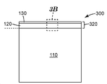
도 3a 및 도 3b는 도 1의 다층 필름(100)의 열가소성 중합체 스킨 층(120) 상에 배치된 배리어 스택(130)을 포함하는 배리어 조립체(300)를 예시한다. 배리어 스택(130) 및 열가소성 중합체 스킨 층(120)은 일체형 보호 층(320)을 형성한다. 일체형 층으로서, 열가소성 중합체 스킨 층(120)에 대한 배리어 스택(130)의 부착성은 층(120)에 대한 제거가능한 캐리어 필름(110)의 부착성보다 실질적으로 더 강하여, 도 3a 및 도 3b의 배리어 조립체(300) 내의 층들의 스택은 제거가능한 캐리어 필름(110)과 열가소성 중합체 스킨 층(120) 사이의 계면에 상응하는 탈층 표면(도 3a 및 도 3b의 점선 참조)을 따라 탈층되는 경향이 있는 것으로 이해되어야 한다.FIGS. 3A and 3B illustrate a
하나 이상의 배리어 스택(130) 및 하나 이상의 열가소성 중합체 스킨 층(120)을 포함하는 일체형 보호 층(320)과 같은 일체형 보호 층은 전형적으로 산소 및/또는 물 침입으로부터의 보호를 제공하기 위해 용도에 필요한 대로 특정 수준의 산소 및 수증기 투과율을 갖도록 형성될 수 있다. 일부 실시 형태에서, 일체형 보호 층(320)은 수증기 투과율(water vapor transmission rate; WVTR)이 38℃ 및 100% 상대 습도에서 약 0.005 g/m2/일 미만; 일부 실시 형태에서, 38℃ 및 100% 상대 습도에서 약 0.0005 g/m2/일 미만; 및 일부 실시 형태에서, 38℃ 및 100% 상대 습도에서 약 0.00005 g/m2/일 미만일 수 있다. 일부 실시 형태에서, 일체형 보호 층(320)은 WVTR이 50℃ 및 100% 상대 습도에서 약 0.05, 0.005, 0.0005, 또는 0.00005 g/m2/일 미만 또는 85℃ 및 100% 상대 습도에서 심지어 약 0.005, 0.0005, 0.00005 g/m2/일 미만일 수 있다. 일부 실시 형태에서, 일체형 보호 층(320)은 산소 투과율이 23℃ 및 90% 상대 습도에서 약 0.005 ㎤/m2/일 미만; 일부 실시 형태에서, 23℃ 및 90% 상대 습도에서 약 0.0005 ㎤/m2/일 미만; 및 일부 실시 형태에서, 23℃ 및 90% 상대 습도에서 약 0.00005 ㎤/m2/일 미만일 수 있다.An integral protective layer, such as an integral
일부 실시 형태에서, 일체형 보호 층(320)은 두께가, 예를 들어, 약 2 밀 (50.8 마이크로미터) 이하, 약 1 밀 (25.4 마이크로미터) 이하, 약 0.5 밀 (12.7 마이크로미터) 이하, 약 0.4 밀 (10.2 마이크로미터) 이하, 또는 약 0.3 밀 (7.6 마이크로미터) 이하; 일부 실시 형태에서, 약 0.005 밀 (0.127 마이크로미터) 이상, 약 0.01 밀 (0.254 마이크로미터) 이상, 약 0.05 밀 (1.27 마이크로미터) 이상, 또는 약 0.1 밀 (2.54 마이크로미터) 이상일 수 있다. 일체형 보호 층(320)의 두께는, 예를 들어, 약 0.01 밀 (0.254 마이크로미터) 내지 약 0.5 밀 (12.7 마이크로미터), 약 0.05 밀 (1.27 마이크로미터) 내지 약 0.5 밀 (12.7 마이크로미터), 또는 약 0.1 밀 (2.54 마이크로미터) 내지 약 0.5 밀 (12.7 마이크로미터)의 범위일 수 있다.In some embodiments, the integral
일체형 보호 층(320)은 배리어 스택(130) 및 열가소성 중합체 스킨 층(120)을 포함한다. 일부 실시 형태에서, 배리어 스택(130)의 두께는, 예를 들어, 약 50 마이크로미터 이하, 20 마이크로미터 이하, 10 마이크로미터 이하, 5 마이크로미터 이하, 또는 3 마이크로미터 이하일 수 있다. 일부 실시 형태에서, 배리어 스택(130)의 두께는 5 nm 이상, 10 nm 이상, 50 nm 이상, 100 nm 이상, 또는 200 nm 이상일 수 있다. 배리어 스택(130)의 두께는, 예를 들어, 약 100 nm 내지 약 5 마이크로미터일 수 있다. 일부 실시 형태에서, 열가소성 중합체 스킨 층(120)의 두께는, 예를 들어, 약 0.5 밀 (12.7 마이크로미터) 이하, 약 0.4 밀 (10.2 마이크로미터) 이하, 약 0.3 밀 (7.6 마이크로미터) 이하, 약 0.2 밀 (5.1 마이크로미터) 이하, 또는 0.1 밀 (2.54 마이크로미터) 이하일 수 있다. 일부 실시 형태에서, 열가소성 중합체 스킨 층(120)의 두께는 약 50 nm 이상, 약 100 nm 이상, 약 200 nm 이상, 약 400 nm 이상, 또는 600 nm 이상일 수 있다. 열가소성 중합체 스킨 층(120)의 두께는, 예를 들어, 약 0.01 밀 (0.254 마이크로미터) 내지 약 0.4 밀 (10.2 마이크로미터)의 범위일 수 있다.The integral
일부 실시 형태에서, 제거가능한 캐리어 필름(110)은 일체형 보호 층(320)보다 2배 이상, 5배 이상, 10배 이상, 20배 이상, 50배 이상, 또는 100배 이상 더 두껍다. 일부 실시 형태에서, 제거가능한 캐리어 필름(110)은 두께가 약 10 밀 (254 마이크로미터) 이하, 약 6 밀 (152 마이크로미터) 이하, 약 4 밀 (102 마이크로미터) 이하, 또는 약 2 밀 (51 마이크로미터) 이하일 수 있다. 일부 실시 형태에서, 제거가능한 캐리어 필름(110)은 두께가 약 100 nm 이상, 약 0.01 밀 (254 nm) 이상, 약 0.05 밀 (1.27 마이크로미터) 이상, 또는 약 0.1 밀 (2.54 마이크로미터) 이상일 수 있다. 제거가능한 캐리어 필름(110)의 두께는, 예를 들어, 약 0.1 밀 (2.54 마이크로미터) 내지 약 4 밀 (102 마이크로미터)의 범위일 수 있다.In some embodiments, the
도 3b에 도시된 실시 형태에서, 배리어 스택(130)은 중합체 층(132) 및 무기 배리어 층(134)을 포함한다. 중합체 층(132)은 제거가능한 캐리어 필름(110) 반대편의 면 상에서 열가소성 중합체 스킨 층(120)과 직접 접촉한다. 중합체 층(132)은 중합체 재료를 열가소성 중합체 스킨 층(120)의 주 표면(124)(또한 도 1 참조)에 적용함으로써 형성될 수 있다. 일부 실시 형태에서, 중합체 층(132)은, 단량체 또는 올리고머의 층을 적용하고 층을 가교결합시켜 원 위치에서(in situ) 중합체를 형성함으로써, 예를 들어, 전자 빔 장치, UV 광원, 전기 방전 장치 또는 다른 적합한 장치를 사용하여 경화되는, 예를 들어, 방사선-가교결합성 단량체의 증발 및 증착에 의해 형성될 수 있다.In the embodiment shown in FIG. 3B, the
일부 실시 형태에서, 배리어 스택(130)은 다양한 순서로 배열된 하나 이상의 중합체 층(132) 및 하나 이상의 무기 배리어 층(134)을 포함할 수 있다. 배리어 스택(130)은 열가소성 중합체 스킨 층(120) 상에 배치되어, 예를 들어, 일부 실시 형태에서, 스킨 층(120)/중합체 층/무기 배리어 층의 구조를 형성할 수 있으며; 일부 실시 형태에서, 구조는 스킨 층(120)/무기 배리어 층/중합체 층일 수 있고; 일부 실시 형태에서, 바람직한 구조는 스킨 층(120)/제1 중합체 층/무기 배리어 층/제2 중합체 층일 수 있으며, 이때, 제1 및 제2 중합체 층은 동일하거나 상이한 조성을 가질 수 있다.In some embodiments, the
예시적인 유용한 배리어 스택은, 예를 들어, 원자층 침착(atomic layer deposition; ALD), 열증발, 스퍼터링, 화학 증착(chemical vapor deposition; CVD), 플라즈마 강화 CVD 등에 의해 제조된 무기 필름을 포함할 수 있다. 유용한 배리어 스택은 전형적으로 가요성이고 투명할 수 있다. 일부 실시 형태에서, 유용한 배리어 스택은 무기/유기 다층을 포함할 수 있다. 무기/유기 다층을 포함하는 가요성 울트라-배리어(ultra-barrier) 필름이, 예를 들어, 미국 특허 출원 공개 제2012/0003451호 (와이겔(Weigel) 등), 미국 특허 제5,440,446호 (쇼(Shaw) 등), 미국 특허 제6,231,939호 (쇼 등), 미국 특허 제7,980,910호 (패디야스(Padiyath) 등), 및 국제특허 공개 WO/2014/028678호 (나흐티갈(Nachtigal) 등)에 기술되어 있으며, 이들은 본 명세서에 참고로 포함된다.Exemplary useful barrier stacks may include inorganic films prepared by, for example, atomic layer deposition (ALD), thermal evaporation, sputtering, chemical vapor deposition (CVD), plasma enhanced CVD, have. Useful barrier stacks are typically flexible and transparent. In some embodiments, useful barrier stacks may include inorganic / organic multilayers. Flexible ultra-barrier films comprising inorganic / organic multilayers are disclosed, for example, in U.S. Patent Application Publication No. 2012/0003451 (Weigel et al.), U.S. Patent No. 5,440,446 (Show Shaw et al., U.S. Patent No. 6,231,939 (Show et al.), U.S. Patent No. 7,980,910 (Padiyath et al.), And International Patent Publication WO / 2014/028678 (Nachtigal et al. , Which are incorporated herein by reference.
무기 배리어 층(134)은 열가소성 중합체 스킨 층(120) 반대편의 면 상에서 중합체 층(132)과 친밀하게 접촉한다. 무기 배리어 층(134)은, 예를 들어, 금속, 금속 산화물, 금속 질화물, 금속 탄화물, 금속 산질화물, 금속 산붕화물, 및 이들의 조합을 포함하는 다양한 재료로부터 형성될 수 있다. 예시적인 금속 산화물에는 산화규소, 예를 들어, 실리카, 산화알루미늄, 예를 들어, 알루미나, 산화티타늄, 예를 들어, 티타니아, 산화인듐, 산화주석, 산화인듐주석 (ITO), 산화탄탈륨, 산화지르코늄, 산화니오븀, 및 이들의 조합이 포함된다. 다른 예시적인 재료에는 탄화붕소, 탄화텅스텐, 탄화규소, 질화알루미늄, 질화규소, 질화붕소, 산질화알루미늄, 산질화규소, 산질화붕소, 산붕화지르코늄, 산붕화티타늄, 및 이들의 조합이 포함된다. 일부 실시 형태에서, 무기 배리어 층은 ITO, 산화규소, 또는 산화알루미늄 중 적어도 하나를 포함할 수 있다. 일부 실시 형태에서, 각각의 원소 성분의 상대적인 비율을 적절히 선택하면, ITO가 전기 전도성이 될 수 있다. 무기 배리어 층은, 예를 들어, 스퍼터링 (예를 들어, 캐소드 또는 평면 마그네트론 스퍼터링, 듀얼 AC 평면 마그네트론 스퍼터링 또는 듀얼 AC 회전성 마그네트론 스퍼터링), 증발 (예를 들어, 저항성 또는 전자빔 증발, 및 이온빔 및 플라즈마 지원 침착을 비롯한 저항성 또는 전자빔 증발의 에너지 강화 유사물), 화학 증착, 플라즈마 강화 화학 증착, 원자층 침착 및 도금(plating)과 같은 박막 침착 분야에서 이용되는 기술을 사용하여 형성될 수 있다. 일부 실시 형태에서, 무기 배리어 층은 스퍼터링, 예를 들어, 반응성 스퍼터링을 사용하여 형성될 수 있다. 통상적인 증착 공정과 같은 더 낮은 에너지의 기술과 비교하여 스퍼터링과 같은 높은 에너지의 침착 기술에 의해 무기 층이 형성될 때 향상된 배리어 특성이 관찰될 수 있다. 이론에 의해 구애됨이 없이, 향상된 특성은 더 큰 운동 에너지로 기재에 도달하는 응축 화학종(condensing species)으로 인한 것이며, 이는 압밀의 결과로서 더 낮은 공극 분율로 이어지는 것으로 여겨진다.The
일부 실시 형태에서, 무기 배리어 층은 원자층 침착(ALD)을 사용하여 형성될 수 있다. 향상된 배리어 특성이 이러한 침착 방법과 관련된 낮은 결함 발생률로 관찰될 수 있다.In some embodiments, the inorganic barrier layer may be formed using atomic layer deposition (ALD). Improved barrier properties can be observed with a low defect incidence associated with this deposition method.
중합체 층(132)과 무기 배리어 층(134)은 다이애드(dyad)로 칭해질 수 있다. 배리어 스택(130)에 대해 오직 하나의 다이애드(즉, 도 3b에서 중합체 층(132)과 무기 배리어 층(134))만 도시되어 있지만, 배리어 스택(130)은 중합체 및 무기 재료의 추가적인 교번하는 층들을 포함할 수 있는 것으로 이해되어야 한다. 배리어 스택에 대한 예시적인 재료 및 구성 방법이 미국 특허 제5,440,446호; 미국 특허 제5,877,895호; 미국 특허 제6,010,751호; 미국 특허 출원 공개 제2003/0029493호; 및 대리인 관리 번호 제69821US002호 및 제66737US002호 (이들 모두는 본 명세서에 참고로 포함됨) 및 본 발명의 실시예에 확인되어 있다.The
도 4a에 예시된 바와 같이, 배리어 조립체(300)는 전자 장치(150)의 주 표면에 적용된다. 전자 장치(150)는 하나 이상의 수분 또는 산소 민감성 성분을 포함할 수 있다. 전자 장치(150)는, 예를 들어, 산소 및/또는 물 침입으로부터의 보호를 필요로 하는, 유기 발광 다이오드 (OLED) 또는 유기 및 무기 광기전 장치 (PV)일 수 있다. 배리어 스택(130)은 접착제 층(140)에 의해 전자 장치(150)에 라미네이팅된다. 접착제 층(140)의 두께는, 예를 들어, 약 0.1 밀 내지 약 1 밀 (0.003 mm 내지 0.03 mm)로 달라질 수 있다.As illustrated in FIG. 4A, the
일부 실시 형태에서, 접착제 층(140)은, 예를 들어, 광학적으로 투명한 접착제 (OCA), 또는 배리어 접착제일 수 있다. 일부 실시 형태에서, OCA는 원 위치에서 광학적으로 투명한 임의의 비교적 연질의 감압 접착제 재료를 포함할 수 있다. 즉, 감압 접착제 재료는 자유 직립(free standing) 상태에서 그 자체로는 광학적으로 투명하지 않을 수 있지만, 일단 라미네이트 내에 포함되면 광학적으로 투명한 상태 및 라미네이트의 층들을 임의의 매우 다양한 기후 조건에 걸쳐 변경되지 않은 형태로 유지하기에 충분한 접착력을 가질 수 있다. 감압 접착제 조성물은 아크릴레이트 또는 아크릴 공중합체 및 삼원공중합체에 기초할 수 있다. 일부 실시 형태에서, 광학적으로 투명한 접착제는, 예를 들어, 천연 고무, 합성 고무, 스티렌 블록 공중합체, (메트)아크릴 블록 공중합체, 폴리비닐 에테르, 폴리올레핀, 및 폴리(메트)아크릴레이트에 기초한 것들을 포함할 수 있다. 용어 (메트)아크릴레이트 및 (메트)아크릴은 아크릴레이트 및 메타크릴레이트 둘 모두를 포함할 수 있다. 예시적인 OCA가 국제특허 공개 WO 2013/025330호 (로토(Rotto) 등)에 기술되어 있으며, 이는 본 명세서에 참고로 포함된다. 일부 실시 형태에서, 배리어 접착제는 약 300,000 g/몰 초과의 중량 평균 분자량을 갖는 제1 폴리아이소부틸렌 수지, 및 다작용성 (메트)아크릴레이트 단량체를 포함하는 조성을 가질 수 있다. 배리어 접착제 조성물에는 점착부여제(tackifier)가 실질적으로 없을 수 있다. 예시적인 배리어 접착제는 미국 특허 출원 공개 제2011/0105637호 (푸지타(Fujita) 등)에 기술되어 있으며, 이는 본 명세서에 참고로 포함된다. 일부 실시 형태에서, 배리어 접착제는 a) 50 중량% 초과의 비-작용성 아이소부틸렌 (공)중합체, b) 0.25 내지 20 중량%의 아민-작용성 폴리(아이소부틸렌) 중합체, c) 0 내지 10 중량%의 산-작용성 (메트)아크릴레이트 공중합체, d) 0 내지 40 중량%의 점착부여제; 및 e) 0 내지 40 중량%의 가소제를 포함하는 조성을 가질 수 있다. 예시적인 배리어 접착제는 미국 특허 제8,663,407호 (졸리(Joly) 등)에 기술되어 있으며, 이는 본 명세서에 참고로 포함된다.In some embodiments, the
선택적으로, 접착제 층(140)은 임의의 통상적인 시트 재료를 포함하는 이형 라이너를 가질 수 있다. 이형 라이너는 접착제 층(140)의 노출된 표면에 대한 보호를 제공할 수 있다. 이형 라이너는 그가 적용되는 접착제 층(140)의 표면에 대해 일시적인 약한 접착력을 가질 수 있으며, 따라서, 배리어 조립체(300)의 표면에 부착하기 위한 접착제의 변경되지 않은 층을 남기도록 표면으로부터 깨끗하게 스트리핑될 수 있다.Alternatively, the
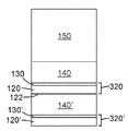
배리어 조립체(300)를 전자 장치(150)에 부착한 후에, 제거가능한 캐리어 필름(110)을 탈층 표면(예를 들어, 도 4b에 도시된 바와 같이, 112 및 122)을 따라 탈층시킴으로써, 제거가능한 캐리어 필름(110)을 배리어 조립체(300)의 나머지로부터 제거할 수 있다. 열가소성 중합체 스킨 층(120) 및 배리어 스택(130)을 포함하는 일체형 보호 층(320)은 전자 장치(150)의 주 표면 상에 남아서 보호를 제공한다. 동일한 방식으로, 제2 일체형 보호 층(320')이 접착제(140')에 의해 제1 일체형 보호 층(320)의 주 표면(122)에 부착될 수 있다. 제2 일체형 보호 층(320')은 열가소성 중합체 스킨 층(120') 및 배리어 스택(130')을 포함하며, 이들은 제1 일체형 보호 층(320)과 비교하여 동일하거나 상이한 조성을 가질 수 있다. 일부 실시 형태에서, 3개 이상의 일체형 보호 층이 전자 장치(150)의 주 표면 위에 놓일 수 있다.After attaching the
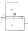
도 5는 접착제를 사용하지 않고 배리어 조립체(300)를 광전자 장치(250)의 주 표면(252) 에 직접 적용하는 것을 예시한다. 배리어 스택(130)은, 배리어 스택(130)과 광전자 장치(250) 사이에 어떠한 접착제도 없이 광전자 장치(250)의 주 표면(252)에 직접 부착된다. 주 표면(252)에 대한 배리어 스택(130)의 부착성은 열가소성 중합체 스킨 층(120)에 대한 제거가능한 캐리어 필름(110)의 부착성보다 실질적으로 더 강할 수 있어서, 캐리어 필름(110)은 캐리어 필름(110)과 열가소성 중합체 스킨 층(120) 사이의 계면에 상응하는 탈층 표면(도 5의 점선 참조)을 따라 전자 장치(250)로부터 비가역적으로 탈층되는 경향이 있다. 일부 실시 형태에서, 광전자 장치(250)는 주 표면(252)이 예컨대 내부에 분산된 양자점을 갖는 중합체 매트릭스 층일 수 있는 광 변환 장치일 수 있다. 중합체 매트릭스 층은 두께가, 예를 들어, 약 0.1 밀 (2.54 마이크로미터) 내지 약 10 밀 (254 마이크로미터)의 범위일 수 있다. 중합체 매트릭스 층은, 예를 들어, 메타크릴레이트 중합체, 에폭시 중합체 및 광개시제를 포함할 수 있다. 일부 실시 형태에서, 중합체 매트릭스 층은 배리어 조립체(300)와 같은 제1 배리어 조립체의 주 표면에 적용될 수 있으며, 제2 배리어 조립체는 제1 배리어 조립체 반대편 면 상에서 중합체 매트릭스 층에 직접 부착될 수 있다. 제1 및 제2 배리어 조립체의 제거가능한 캐리어 필름(110)은 적절한 단계에서 제거되어 광전자 장치(250) 상에 일체형 보호 층(320)을 남길 수 있다. 배리어 필름 및 양자점 층을 포함하는 예시적인 양자점 필름이 국제특허 공개 WO 2014/113562호 (넬슨(Nelson) 등)에 기술되어 있으며, 이는 본 명세서에 참고로 포함된다.Figure 5 illustrates applying the
본 발명의 다양한 예시적인 실시예가 이제 특히 도면을 참조하여 기술될 것이다. 본 발명의 예시적인 실시 형태는 본 발명의 사상 및 범주로부터 벗어남이 없이 다양한 수정 및 변경을 취할 수 있다. 따라서, 본 발명의 실시 형태는 하기에 기술되는 예시적인 실시 형태에 한정되는 것이 아니라, 청구범위에 기재된 한정 및 그의 임의의 등가물에 의해 좌우되어야 한다는 것이 이해되어야 한다.Various illustrative embodiments of the present invention will now be described with particular reference to the drawings. The illustrative embodiments of the present invention can make various changes and modifications without departing from the spirit and scope of the invention. Accordingly, it is to be understood that the embodiments of the present invention are not limited to the exemplary embodiments described below, but rather should be governed by the limitations set forth in the claims and any equivalents thereof.
예시적인 실시 형태의 목록List of exemplary embodiments
실시 형태 1은,In the first embodiment,
서로 반대편에 있는 제1 및 제2 주 표면을 갖는 열가소성 중합체 스킨 층;A thermoplastic polymer skin layer having first and second major surfaces opposite to each other;
스킨 층의 제1 주 표면 상에 코팅된 배리어 스택으로서, 스킨 층 및 배리어 스택은 일체형 보호 층을 형성하고, 일체형 보호 층은 두께가 약 0.5 밀 (12.7 마이크로미터) 이하인, 상기 배리어 스택; 및A barrier stack coated on a first major surface of a skin layer, the skin layer and the barrier stack forming an integral protective layer, the integral protective layer having a thickness of about 0.5 mils (12.7 micrometers) or less; And
스킨 층의 제2 주 표면에 이형가능하게 부착된 주 표면을 갖는 제거가능한 캐리어 필름으로서, 제거가능한 캐리어 필름은 일체형 보호 층을 지지하도록 구성되는, 상기 제거가능한 캐리어 필름을 포함하는, 물품이다.A removable carrier film having a major surface releasably attached to a second major surface of a skin layer, wherein the removable carrier film is configured to support the integral protective layer.
실시 형태 2는, 배리어 스택은 무기 배리어 층 및 제1 가교결합된 중합체 층을 포함하는, 실시 형태 1의 물품이다.Embodiment 2 is the article of Embodiment 1, wherein the barrier stack comprises an inorganic barrier layer and a first cross-linked polymer layer.
실시 형태 3은, 제거가능한 캐리어 필름은 일체형 보호 층보다 2배 이상 더 두꺼운, 실시 형태 1 또는 실시 형태 2의 물품이다.Embodiment 3 is the article of Embodiment 1 or Embodiment 2 in which the removable carrier film is twice as thick as the integral protective layer.
실시 형태 4는, 일체형 보호 층의 두께는 약 0.01 밀 (0.254 마이크로미터) 내지 약 0.5 밀 (12.7 마이크로미터)의 범위인, 실시 형태 1 내지 실시 형태 3 중 어느 한 실시 형태의 물품이다.Embodiment 4 is an article according to any one of Embodiments 1 to 3, wherein the thickness of the integral protective layer is in the range of about 0.01 mils (0.254 micrometers) to about 0.5 mils (12.7 micrometers).
실시 형태 5는, 열가소성 중합체 스킨 층의 두께는 약 0.01 밀 (0.254 마이크로미터) 내지 약 0.5 밀 (12.7 마이크로미터)의 범위인, 실시 형태 1 내지 실시 형태 4 중 어느 한 실시 형태의 물품이다.Embodiment 5 is an article according to any one of Embodiments 1 to 4 wherein the thickness of the thermoplastic polymer skin layer is in a range from about 0.01 mil (0.254 micrometer) to about 0.5 mil (12.7 micrometer).
실시 형태 6은, 배리어 스택의 두께는 약 5 nm 내지 약 10 마이크로미터의 범위인, 실시 형태 1 내지 실시 형태 5 중 어느 한 실시 형태의 물품이다.Embodiment 6 is an article according to any one of Embodiments 1 to 5, wherein the thickness of the barrier stack is in the range of about 5 nm to about 10 micrometers.
실시 형태 7은, 열가소성 중합체 스킨 층은 폴리에스테르, 폴리올레핀, 폴리아크릴레이트, 폴리아미드, 폴리카르보네이트, 폴리우레탄, 및 폴리스티렌으로 이루어진 군으로부터 선택되는 하나 이상의 열가소성 중합체를 포함하는, 실시 형태 1 내지 실시 형태 6 중 어느 한 실시 형태의 물품이다.Embodiment 7 is an embodiment 7 wherein the thermoplastic polymer skin layer comprises at least one thermoplastic polymer selected from the group consisting of polyesters, polyolefins, polyacrylates, polyamides, polycarbonates, polyurethanes, and polystyrenes. It is an article according to any one of the embodiments 6 to 10. [
실시 형태 8은, 열가소성 중합체 스킨 층은 폴리에틸렌 테레프탈레이트 (PET) 또는 폴리에틸렌 나프탈레이트 (PEN)를 포함하는, 실시 형태 7의 물품이다.Embodiment 8 is the article of Embodiment 7, wherein the thermoplastic polymer skin layer comprises polyethylene terephthalate (PET) or polyethylene naphthalate (PEN).
실시 형태 9는, 제거가능한 캐리어 필름은 스킨 층의 제2 주 표면에 부착된 최전방 층 및 그 반대편 면 상에서 최전방 층에 부착된 내부 층을 포함하는 중합체 층들의 스택을 포함하는, 실시 형태 1 내지 실시 형태 8 중 어느 한 실시 형태의 물품이다.Embodiment 9: The method of any one of Embodiments 1 to 6, wherein the removable carrier film comprises a stack of polymer layers including a foremost layer attached to a second major surface of the skin layer and an inner layer attached to the foremost layer on the opposite side thereof. Is an article according to any one of the eight modes.
실시 형태 10은, 최전방 층은 프로필렌 공중합체와 스티렌성 블록 공중합체의 블렌드, 프로필렌 공중합체와 에틸렌 알파 올레핀 공중합체의 블렌드, 또는 프로필렌 공중합체와 올레핀 블록 공중합체의 블렌드를 포함하는 중합체 조성물 B를 갖는, 실시 형태 9의 물품이다.In Embodiment 10, the foremost layer comprises a polymer composition B comprising a blend of a propylene copolymer and a styrenic block copolymer, a blend of a propylene copolymer and an ethylene alpha olefin copolymer, or a blend of a propylene copolymer and an olefin block copolymer Is the article of the ninth embodiment.
실시 형태 11은, 내부 층은 반결정질 폴리에스테르를 포함하는 중합체 조성물 A를 갖는, 실시 형태 9 또는 실시 형태 10의 물품이다.Embodiment 11 is the article of Embodiment 9 or Embodiment 10, wherein the inner layer has a polymer composition A comprising a semi-crystalline polyester.
실시 형태 12는, 최전방 층은 최전방 층과 내부 층 사이의 조성물 C를 갖는 층간 층(interlayer layer)을 통해 내부 층에 부착되고, 최전방 층은 내부 층보다 스킨 층의 제2 주 표면에 대해 더 약한 부착성을 가져, 제거가능한 캐리어 필름은 최전방 층과 스킨 층 사이의 계면에 상응하는 탈층 표면을 따라 일체형 보호 층으로부터 비가역적으로 탈층되는 경향이 있는, 실시 형태 9 내지 실시 형태 11 중 어느 한 실시 형태의 물품이다.Embodiment 12 is characterized in that the foremost layer is attached to the inner layer through an interlayer layer having a composition C between the foremost layer and the inner layer and the foremost layer is weaker against the second major surface of the skin layer than the inner layer Embodiments of Embodiments Nos. 9 to 11, in which the removable carrier film tends to irreversibly detach from the integral protective layer along the surface of the demineralization layer corresponding to the interface between the foremost layer and the skin layer, Lt; / RTI >
실시 형태 13은, 스킨 층의 제2 주 표면에 대한 최전방 중합체 층의 부착성은 제1 박리력에 의해 특징지어지고, 하부 층에 대한 최전방 중합체 층의 부착성은 제2 박리력에 의해 특징지어지며, 제2 박리력은 제1 박리력의 2배 이상인, 실시 형태 12의 물품이다.In Embodiment 13, the adhesion of the foremost polymer layer to the second main surface of the skin layer is characterized by the first peel force, and the adhesion of the foremost polymer layer to the lower layer is characterized by the second peel force, The second peeling force is the article of the twelfth embodiment, which is at least twice the first peeling force.
실시 형태 14는, 일체형 보호 층은 수증기 투과율 (WVTR)이 38℃ 및 100% 상대 습도에서 약 0.005 g/m2/일 미만인, 실시 형태 1 내지 실시 형태 13 중 어느 한 실시 형태의 물품이다.Embodiment 14 is the article of any one of Embodiments 1 to 13 wherein the integral protective layer has a water vapor permeability (WVTR) of less than about 0.005 g / m 2 / day at 38 캜 and 100% relative humidity.
실시 형태 15는, 주 표면 및 실시 형태 1 내지 실시 형태 14 중 어느 한 실시 형태의 물품을 포함하는 광전자 장치로서, 물품의 배리어 스택이 광전자 장치의 주 표면에 부착되는, 광전자 장치이다.Embodiment 15 is an optoelectronic device including a main surface and an article of any one of Embodiments 1 to 14, wherein the barrier stack of the article is attached to the main surface of the optoelectronic device.
실시 형태 16은, 광전자 장치로서,Embodiment 16 is an optoelectronic device,
주 표면;Main surface;
서로 반대편에 있는 제1 및 제2 주 표면을 갖는 열가소성 중합체 스킨 층; 및A thermoplastic polymer skin layer having first and second major surfaces opposite to each other; And
스킨 층의 제1 주 표면 상에 코팅된 배리어 스택으로서, 스킨 층 및 배리어 스택은 일체형 보호 층을 형성하고, 일체형 보호 층은 두께가 약 0.5 밀 (12.7 마이크로미터) 이하인, 배리어 스택을 포함하며;A barrier stack coated on a first major surface of a skin layer, the skin layer and barrier stack forming an integral protective layer, wherein the integral protective layer comprises a barrier stack having a thickness of about 0.5 mils (12.7 micrometers) or less;
이때 배리어 스택은 광전자 장치의 주 표면에 부착되는, 광전자 장치이다.Wherein the barrier stack is attached to the main surface of the optoelectronic device.
실시 형태 17은, 광전자 장치의 주 표면은 유리 표면이 아닌, 실시 형태 15 또는 실시 형태 16의 광전자 장치이다.Embodiment 17 is an optoelectronic device according to Embodiment 15 or Embodiment 16, in which the main surface of the optoelectronic device is not a glass surface.
실시 형태 18은, 접착제 층을 추가로 포함하며, 이때 배리어 스택은 접착제 층에 의해 광전자 장치의 주 표면에 부착되는, 실시 형태 15 내지 실시 형태 17 중 어느 한 실시 형태의 광전자 장치이다.Embodiment 18 is an optoelectronic device according to any one of Embodiment 15 to Embodiment 17, further comprising an adhesive layer, wherein the barrier stack is attached to the main surface of the photoelectric device by an adhesive layer.
실시 형태 19는, 접착제 층은 광학적으로 투명한 접착제 또는 배리어 접착제를 포함하는, 실시 형태 18의 광전자 장치이다.Embodiment 19 is the optoelectronic device of Embodiment 18, wherein the adhesive layer comprises an optically transparent adhesive or a barrier adhesive.
실시 형태 20은, 광전자 장치는 주 표면을 포함하는 유기 발광 다이오드(OLED) 장치이며, 배리어 스택은 접착제 층을 통해 OLED의 주 표면에 부착되는, 실시 형태 15 내지 실시 형태 19 중 어느 한 실시 형태의 광전자 장치이다.Embodiment 20 is an organic light emitting diode (OLED) device in which the optoelectronic device is a main surface, and the barrier stack is attached to the main surface of the OLED through an adhesive layer. Optoelectronic devices.
실시 형태 21은, 광전자 장치는 중합체 매트릭스 층 내에 매립된 양자점 입자를 갖는 중합체 매트릭스 층을 포함하는 광 변환 장치이며, 주 표면은 중합체 매트릭스 층의 표면이고, 배리어 스택은 배리어 스택과 중합체 매트릭스 층 사이에 어떠한 접착제도 없이 중합체 매트릭스 층의 표면에 직접 부착되는, 실시 형태 15 내지 실시 형태 20 중 어느 한 실시 형태의 광전자 장치이다.Embodiment 21: A phototransistor device according to embodiment 21, wherein the optoelectronic device is a photoconversion device comprising a polymer matrix layer having quantum dot particles embedded in a polymer matrix layer, the major surface being the surface of the polymer matrix layer, The optoelectronic device according to any one of the fifteenth to twentieth embodiments is directly attached to the surface of the polymer matrix layer without any adhesive.
실시 형태 22는, 실시 형태 1 내지 실시 형태 14 중 어느 한 실시 형태의 물품을 사용하는 방법으로서,Embodiment 22 A method of using an article according to any one of Embodiment Modes 1 to 14,
기재를 제공하는 단계;Providing a substrate;
실시 형태 1의 물품의 일체형 보호 층을 기재에 부착하는 단계; 및Attaching the integral protective layer of the article of Embodiment 1 to a substrate; And
제거가능한 캐리어 필름을 일체형 보호 층으로부터 제거하는 단계를 포함하는, 방법이다.Removing the removable carrier film from the integral protective layer.
실시 형태 23은,Embodiment 23 In Embodiment 23,
주 표면을 갖는 제거가능한 캐리어 필름을 제공하는 단계;Providing a removable carrier film having a major surface;
제거가능한 캐리어 필름의 주 표면 상에 배치되는 열가소성 중합체 스킨 층을 제공하는 단계로서, 열가소성 중합체 스킨 층은 서로 반대편에 있는 제1 및 제2 주 표면을 갖고, 열가소성 중합체 스킨 층의 제2 주 표면은 제거가능한 캐리어 필름의 주 표면에 이형가능하게 부착되는, 단계; 및Providing a thermoplastic polymer skin layer disposed on a major surface of a removable carrier film, wherein the thermoplastic polymer skin layer has first and second major surfaces opposite to each other, and a second major surface of the thermoplastic polymer skin layer Releasably affixed to the main surface of the removable carrier film; And
스킨 층의 제1 주 표면 상에 배리어 스택을 코팅하는 단계로서, 열가소성 중합체 스킨 층 및 배리어 스택은 약 0.5 밀 (12.7 마이크로미터) 이하의 두께를 갖는 일체형 보호 층을 형성하는, 단계를 포함하는, 방법이다.Coating a barrier stack on a first major surface of the skin layer, wherein the thermoplastic polymer skin layer and the barrier stack form an integral protective layer having a thickness of about 0.5 mils (12.7 micrometers) or less. Method.
실시 형태 24는, 제거가능한 캐리어 필름과 일체형 보호 층 사이의 계면을 따른 탈층에 의해 일체형 보호 층으로부터 제거가능한 캐리어 필름을 제거하는 단계를 추가로 포함하는, 실시 형태 23의 방법이다.Embodiment 24 is the method of embodiment 23 further comprising removing the removable carrier film from the integral protective layer by a delamination along the interface between the removable carrier film and the integral protective layer.
실시 형태 25는, 배리어 스택은 무기 배리어 층 및 가교결합된 중합체 층을 포함하고, 가교결합된 중합체 층은 열가소성 중합체 스킨 층의 제1 주 표면 상에 배치되는, 실시 형태 23 또는 실시 형태 24의 방법이다.Embodiment 25 is a method according to embodiment 23 or embodiment 24 wherein the barrier stack comprises an inorganic barrier layer and a crosslinked polymer layer and the crosslinked polymer layer is disposed on a first major surface of the thermoplastic polymer skin layer to be.
실시 형태 26은, 제거가능한 캐리어 필름은 일체형 보호 층보다 2배 이상 더 두꺼운, 실시 형태 23 내지 실시 형태 25 중 어느 한 실시 형태의 방법이다.Embodiment 26 is the method according to any one of Embodiment 23 to Embodiment 25, wherein the removable carrier film is twice as thick as the integral type protective layer.
실시 형태 27은, 일체형 보호 층의 두께는 약 0.01 밀 (0.254 마이크로미터) 내지 약 0.5 밀 (12.7 마이크로미터)의 범위인, 실시 형태 23 내지 실시 형태 26 중 어느 한 실시 형태의 방법이다.Embodiment 27 is the method of any one of Embodiment 23 to Embodiment 26, wherein the thickness of the integral protective layer is in the range of about 0.01 mils (0.254 micrometers) to about 0.5 mils (12.7 micrometers).
실시 형태 28은, 열가소성 중합체 스킨 층의 두께는 약 0.01 밀 (0.254 마이크로미터) 내지 약 0.5 밀 (12.7 마이크로미터)의 범위인, 실시 형태 23 내지 실시 형태 27 중 어느 한 실시 형태의 방법이다.Embodiment 28 is the method of any one of embodiments 23-27, wherein the thickness of the thermoplastic polymer skin layer is in a range of about 0.01 mils (0.254 micrometers) to about 0.5 mils (12.7 micrometers).
실시 형태 29는, 배리어 스택의 두께는 약 5 nm 내지 약 10 마이크로미터의 범위인, 실시 형태 23 내지 실시 형태 28 중 어느 한 실시 형태의 방법이다.Embodiment 29 is the method of any one of Embodiment 23 to Embodiment 28, wherein the thickness of the barrier stack is in a range of about 5 nm to about 10 micrometers.
실시 형태 30은, 열가소성 중합체 스킨 층은 폴리에스테르, 폴리올레핀, 폴리아크릴레이트, 폴리아미드, 폴리카르보네이트, 폴리우레탄, 및 폴리스티렌으로 이루어진 군으로부터 선택되는 하나 이상의 열가소성 중합체를 포함하는, 실시 형태 23 내지 실시 형태 29 중 어느 한 실시 형태의 방법이다.Embodiment 30 is an embodiment 30 wherein the thermoplastic polymer skin layer comprises at least one thermoplastic polymer selected from the group consisting of polyesters, polyolefins, polyacrylates, polyamides, polycarbonates, polyurethanes, and polystyrenes. The method of any one of the twenty-ninth embodiments.
실시 형태 31은, 열가소성 중합체 스킨 층은 폴리에틸렌 테레프탈레이트 (PET) 또는 폴리에틸렌 나프탈레이트 (PEN)를 포함하는, 실시 형태 30의 방법이다.Embodiment 31 is the method of Embodiment 30, wherein the thermoplastic polymer skin layer comprises polyethylene terephthalate (PET) or polyethylene naphthalate (PEN).
실시 형태 32는, 제거가능한 캐리어 필름은 스킨 층의 제2 주 표면에 부착된 최전방 층 및 그 반대편 면 상에서 최전방 층에 부착된 내부 층을 포함하는 중합체 층들의 스택을 포함하는, 실시 형태 30 또는 실시 형태 31의 방법이다.Embodiment 32. The method of embodiment 30 wherein the removable carrier film comprises a stack of polymeric layers comprising a topmost layer attached to a second major surface of the skin layer and an inner layer attached to the foremost layer on an opposite surface thereof. Lt; / RTI >
실시 형태 33은, 최전방 층은 프로필렌 공중합체와 스티렌성 블록 공중합체의 블렌드, 프로필렌 공중합체와 에틸렌 알파 올레핀 공중합체의 블렌드, 또는 프로필렌 공중합체와 올레핀 블록 공중합체의 블렌드를 포함하는 중합체 조성물 B를 갖는, 실시 형태 32의 방법이다.Embodiment 33 is characterized in that the foremost layer comprises a polymer composition B comprising a blend of a propylene copolymer and a styrenic block copolymer, a blend of a propylene copolymer and an ethylene alpha olefin copolymer, or a blend of a propylene copolymer and an olefin block copolymer, Lt; / RTI >
실시 형태 34는, 내부 층은 반결정질 폴리에스테르를 포함하는 중합체 조성물 A를 갖는, 실시 형태 32 또는 실시 형태 33의 방법이다.Embodiment 34 is the method of embodiment 32 or embodiment 33, wherein the inner layer has a polymer composition A comprising a semi-crystalline polyester.
실시 형태 35는, 최전방 층은 최전방 층과 내부 층 사이의 조성물 C를 갖는 층간 층을 통해 내부 층에 부착되고, 최전방 층은 내부 층보다 스킨 층의 제2 주 표면에 대해 더 약한 부착성을 가져, 제거가능한 캐리어 필름은 최전방 층과 스킨 층 사이의 계면에 상응하는 탈층 표면을 따라 일체형 보호 층으로부터 비가역적으로 탈층되는 경향이 있는, 실시 형태 32 내지 실시 형태 34 중 어느 한 실시 형태의 방법이다.Embodiment 35 wherein the foremost layer is attached to the inner layer through an interlayer having a composition C between the foremost layer and the inner layer and the foremost layer has a weaker adhesion to the second major surface of the skin layer than the inner layer , The removable carrier film is a method according to any of the embodiments 32 to 34, wherein the removable carrier film tends to irreversibly delaminate from the integral protective layer along the delamination surface corresponding to the interface between the foremost layer and the skin layer.
실시 형태 36은, 스킨 층의 제2 주 표면에 대한 최전방 중합체 층의 부착성은 제1 박리력에 의해 특징지어지고, 하부 층에 대한 최전방 중합체 층의 부착성은 제2 박리력에 의해 특징지어지며, 제2 박리력은 제1 박리력의 2배 이상인, 실시 형태 35의 방법이다.Embodiment 36. The method according to Embodiment 36, wherein the adhesion of the foremost polymer layer to the second major surface of the skin layer is characterized by a first peel force, and the adhesion of the foremost polymer layer to the lower layer is characterized by a second peel force, And the second peeling force is at least twice the first peeling force.
실시 형태 37은, 일체형 보호 층은 수증기 투과율 (WVTR)이 38℃ 및 100% 상대 습도에서 약 0.005 g/m2/일 미만인, 실시 형태 23 내지 실시 형태 36 중 어느 한 실시 형태의 방법이다.Embodiment 37 is the method of any of embodiments 23 to 36 wherein the integral protective layer has a water vapor transmission rate (WVTR) of less than about 0.005 g / m 2 / day at 38 캜 and 100% relative humidity.
실시 형태 38은, 제1 가교결합된 중합체 층은 열가소성 중합체 스킨 층의 제1 주 표면 상에 배치되고, 무기 배리어 층은 제1 가교결합된 중합체 층 상에 배치되는, 실시 형태 2의 물품이다.Embodiment 38 is the article of Embodiment 2 wherein the first crosslinked polymeric layer is disposed on the first major surface of the thermoplastic polymeric skin layer and the inorganic barrier layer is disposed on the first crosslinked polymeric layer.
실시 형태 39는, 배리어 스택은 제2 가교결합된 중합체 층을 추가로 포함하고, 무기 배리어 층은 제1 및 제2 가교결합된 중합체 층들에 의해 개재되는, 실시 형태 38의 물품이다.Embodiment 39 is the article of embodiment 38, wherein the barrier stack further comprises a second cross-linked polymeric layer and the inorganic barrier layer is interposed by first and second cross-linked polymeric layers.
실시 형태 40은, 무기 배리어 층은 열가소성 중합체 스킨 층의 제1 주 표면 상에 배치되고, 제1 가교결합된 중합체 층은 무기 배리어 층 상에 배치되는, 실시 형태 2의 물품이다Embodiment 40 is the article of Embodiment 2 wherein the inorganic barrier layer is disposed on the first major surface of the thermoplastic polymer skin layer and the first crosslinked polymer layer is disposed on the inorganic barrier layer
본 발명의 실시가 이하의 상세한 실시예들과 관련하여 추가로 설명될 것이다. 이들 실시예는 다양한 특정한 그리고 바람직한 실시 형태 및 기술을 추가로 예시하기 위해 제공된다. 그러나, 본 발명의 범주 내에 있으면서 많은 변형 및 수정이 이루어질 수 있다는 것을 이해하여야 한다.The practice of the present invention will be further described with reference to the following detailed embodiments. These embodiments are provided to further illustrate various specific and preferred embodiments and techniques. However, it should be understood that many variations and modifications may be made while remaining within the scope of the present invention.
실시예Example
이들 실시예는 단지 예시를 위한 것이며, 첨부된 청구범위의 범주에 대해 과도하게 제한하는 것으로 의도되지 않는다. 본 발명의 넓은 범주를 기술하는 수치 범위 및 파라미터가 근사치임에도 불구하고, 특정 예에 기술된 수치 값은 가능한 한 정확하게 보고된다. 그러나, 임의의 수치 값은 본질적으로 그의 각자의 시험 측정치에서 발견되는 표준 편차로부터 필연적으로 유래하는 소정의 오차를 포함한다. 최소한으로, 그리고 청구범위의 범주에 대한 균등론의 적용을 제한하려는 시도로서가 아니라, 각각의 수치 파라미터는 적어도 보고된 유효 숫자의 숫자의 관점에서 그리고 보통의 반올림 기법을 적용함으로써 해석되어야 한다.These embodiments are for illustrative purposes only and are not intended to be limiting in any way to the scope of the appended claims. Notwithstanding that the numerical ranges and parameters describing the broad scope of the invention are approximations, the numerical values set forth in the specific examples are reported as precisely as possible. However, any numerical value inherently includes a certain error inherently resulting from the standard deviation found in its respective test measurement. At the very least, and not as an attempt to limit the application of the doctrine of equivalents to the scope of the claims, each numerical parameter should at least be construed in light of the number of reported significant digits and by applying ordinary rounding techniques.
재료의 요약Summary of Materials
달리 언급되지 않는 한, 실시예 및 본 명세서의 나머지 부분에서의 모든 부, 백분율, 비 등은 중량 기준이다. 게다가, 표 1은 하기 실시예에 사용된 모든 재료에 대한 약어 및 공급처를 제공한다.Unless otherwise stated, all parts, percentages, ratios, etc. in the examples and the remainder of the specification are by weight. In addition, Table 1 provides abbreviations and sources for all materials used in the following examples.
[표 1][Table 1]

시험 방법Test Methods
본 발명의 실시예 중 일부를 평가하는 데 하기 시험 방법을 사용하였다.The following test methods were used to evaluate some of the embodiments of the present invention.
하기에 기술된 바와 같은 칼슘 부식 시험을 사용하여 수분 배리어 성능을 측정하였다. 먼저, 금속 칼슘의 얇고 불투명한 반사층 (약 100 nm 두께)을 불활성 환경 내에서 유리 슬라이드 상에 열증발시켜 조기 부식을 방지하였다. 동시에, 배리어 접착제의 시트를 실시예에 라미네이팅하였다. 이어서, 접착제를 갖는 샘플을 Ca-코팅된 유리 슬라이드에 라미네이팅하였다. 이어서, 슬라이드를 60℃/90% RH에 노출시켰고, 에이징 동안 상이한 시점에 고해상도 광학 스캐너를 사용하여 슬라이드를 검사하였다. 수분이 보호 층에 침투함에 따라, 금속 칼슘을 부식시켜 금속 칼슘을 불투명한 물질로부터 투명한 산화물로 전환시켰다. 광학 스캐너는 이러한 반응을 슬라이드의 광학 밀도의 손실로서 해석하며, 이러한 특성은 수증기 투과율(WVTR)과 상관 관계가 있다.The moisture barrier performance was measured using a calcium corrosion test as described below. First, a thin, opaque reflective layer of metal calcium (about 100 nm thick) was thermally evaporated on a glass slide in an inert environment to prevent premature corrosion. At the same time, a sheet of barrier adhesive was laminated to the examples. The sample with adhesive was then laminated to a Ca-coated glass slide. The slides were then exposed to 60 [deg.] C / 90% RH and the slides were inspected at different times during aging using a high resolution optical scanner. As moisture penetrated the protective layer, the metal calcium was corroded to convert the metal calcium from an opaque material to a transparent oxide. Optical scanners interpret this response as a loss of the optical density of the slide, which is correlated with the Water Vapor Transmission Rate (WVTR).
모콘 퍼마트랜(MOCON PERMATRAN)-W(등록상표) 700 WVTR 시험 시스템 (미국 미네소타주 미니애폴리스 소재의 모콘 인크.(MOCON Inc.)로부터 구매가능함)을 사용하여, 일부 샘플의 WVTR을 또한 측정하였다. 코팅된 필름의 시트로부터 4 인치 직경의 샘플을 잘라내었고, WVTR의 정상 상태 측정에 도달할 때까지 50℃에서 100% RH로 필름의 한쪽 면을 시험하도록 설정된 장치에 로딩하였다. 이 장비의 최저 검출 한계는 약 0.005 g/m2/일이다.The WVTR of some samples was also measured using a MOCON PERMATRAN-W 700 WVTR test system (available from MOCON Inc., Minneapolis, Minn.). A 4 inch diameter sample was cut from the sheet of coated film and loaded onto a device set to test one side of the film at 50 DEG C and 100% RH until reaching a steady state measurement of the WVTR. The minimum detection limit for this equipment is approximately 0.005 g / m 2 / day.
실시예Example
실시예 1: Example 1 :
실시예 1에서는, 도 2에 도시된 것과 유사한 구조를 갖는 다층 중합체 필름을 형성함으로써, 얇은 열가소성 중합체 스킨 층을 갖는 캐리어 필름 기재를 제조하였다. 층 A (0.2 밀 또는 5 마이크로미터)/층 B (0.5 밀 또는 12.7 마이크로미터)/층 A (0.5 밀 또는 12.7 마이크로미터)/층 B (0.5 밀 또는 12.7 마이크로미터)/층 A (0.2 밀 또는 5 마이크로미터)의 대칭 구조를 갖는 5층 스택을 형성하였다. 최상측 층 A (0.2 밀 또는 5 마이크로미터)는 본 명세서에 논의된 바와 같은 하부 층 B (0.5 밀 또는 12.7 마이크로미터)로부터 제거가능한 얇은 열가소성 중합체 스킨 층이었다. 층 A 및 층 B는 각각 중합체 조성물 A 및 중합체 조성물 B를 가지며, 이들은 서로 공압출가능하였고, 모두 204℃ (400℉) 이상의 온도에서 용융 가공가능하였다. 이들 실시예에 기술된 샘플의 압출 동안 압출기, 다이(die), 및 피드블록(feedblock)을 500 내지 530℉(260 내지 277℃)의 온도로 가열하였다. 하기 중합체 조성물 및 압출기 유량을 사용하였다:In Example 1, a carrier film substrate having a thin thermoplastic polymer skin layer was prepared by forming a multilayer polymer film having a structure similar to that shown in Fig. Layer A (0.2 or 5 micrometers) / layer B (0.5 or 12.7 micrometers) / layer A (0.5 or 12.7 micrometers) / layer B (0.5 or 12.7 micrometers) / layer A 5 < / RTI > micrometer) symmetric structure. The topmost layer A (0.2 mil or 5 micrometers) was a thin thermoplastic polymer skin layer that was removable from the bottom layer B (0.5 mil or 12.7 micron) as discussed herein. Layer A and Layer B had polymer composition A and polymer composition B, respectively, which were coextrudable to each other and were melt processable at temperatures above 204 ° C (400 ° F). During extrusion of the samples described in these examples, the extruder, die, and feedblock were heated to a temperature of 500-530 ° F (260-277 ° C). The following polymer compositions and extruder flow rates were used:
![]()
![]()
![]()
![]()
[표 2][Table 2]

상기 표 2는 층 A (0.2 밀 또는 5 마이크로미터)/층 B (0.5 밀 또는 12.7 마이크로미터)/층 A (0.5 밀 또는 12.7 마이크로미터)/층 B (0.5 밀 또는 12.7 마이크로미터)/층 A (0.2 밀 또는 5 마이크로미터)의 대칭 구조를 갖는 5층 스택을 위한 중합체 조성물 및 압출기 유량을 열거한다.The above Table 2 shows the results of a comparison of the layer A (0.2 mil or 5 micrometer) / layer B (0.5 mil or 12.7 micrometer) / layer A (0.5 mil or 12.7 micrometer) / layer B (0.5 mil or 12.7 micrometer) (0.2 mil or 5 micrometers), and extruder flow rates.
전술된 구조의 기재를 미국 특허 제5,440,446호 (쇼 등) 및 미국 특허 제7,018,713호 (패디야스 등) (둘 모두 본 명세서에 참고로 포함됨)에 기술된 코팅기와 유사한 진공 코팅기에서 베이스 중합체 층 (층 1), 무기 규소 알루미늄 산화물 (SiAlOx) 배리어 층 (층 2), 및 보호 중합체 층 (층 3)의 스택으로 덮어서 배리어 필름 또는 코팅을 제조하였다. 개별 층들은 다음과 같이 형성하였다:The substrate of the above-described structure is coated with a base polymer layer (layer) in a vacuum coater similar to the coating machine described in U.S. Patent No. 5,440,446 (Show et al.) And U.S. Patent No. 7,018,713 (Paddy's et al) 1), an inorganic silicon aluminum oxide (SiAlOx) barrier layer (Layer 2), and a protective polymer layer (Layer 3) to produce a barrier film or coating. The individual layers were formed as follows:
층 1 (베이스 중합체 층): 무한 길이의 366 mm 폭 필름을 롤-투-롤 진공 가공 챔버 내에 로딩하였다. 챔버를 2 × 10⁻⁵ 토르의 압력으로 펌핑 다운(pumped down)시켰다. 필름의 배면(backside)을 -10℃로 냉각된 코팅 드럼과 접촉한 채로 유지하면서 4.9 미터/min의 웨브 속도를 유지하였다. 배면이 드럼과 접촉해 있는 채로, 필름 전면 표면을 0.02 kW의 플라즈마 출력에서 질소 플라즈마로 처리하였다. 이어서, 필름 전면 표면을 트라이사이클로데칸 다이메탄올 다이아크릴레이트 단량체 (미국 펜실베이니아주 엑스턴 소재의 사토머 유에스에이로부터 상표명 "SR833S"로 입수함)로 코팅하였다. 단량체를 코팅 전에 진공 하에서 20 mTorr의 압력까지 탈기시키고, 주사기 펌프 내에 로딩하고, 60 ㎑의 주파수에서 작동하는 초음파 무화기를 통해 260℃에서 유지되는 가열된 기화 챔버 내로 1.33 mL/min의 유량으로 펌핑하였다. 생성된 단량체 증기 스트림은 필름 표면 상에 응축되었고 7.0 ㎸ 및 4 mA에서 작동하는 다중-필라멘트 전자-빔 경화 건(multi-filament electron-beam cure gun)을 사용하여 전자 빔 가교결합하여 750 nm 두께의 베이스 중합체 층을 형성하였다.Layer 1 (base polymer layer): An infinitely long 366 mm wide film was loaded into a roll-to-roll vacuum processing chamber. The chamber was pumped down to a pressure of 2 x 10 < -5 > Torr. The web speed of 4.9 meters / min was maintained while the backside of the film was kept in contact with the coating drum cooled to -10 占 폚. With the back side in contact with the drum, the front surface of the film was treated with a nitrogen plasma at a plasma output of 0.02 kW. The front surface of the film was then coated with tricyclodecane dimethanol diacrylate monomer (available as SR833S from Satomer USA, Exton, Pa.). The monomers were degassed under vacuum prior to coating to a pressure of 20 mTorr, loaded into a syringe pump and pumped through a heated vaporization chamber maintained at 260 DEG C through an ultrasonic atomizer operating at a frequency of 60 kHz at a flow rate of 1.33 mL / min . The resulting monomer vapor stream was condensed on the film surface and electron beam crosslinked using a multi-filament electron-beam cure gun operating at 7.0 kV and 4 mA to form a 750 nm thick To form a base polymer layer.
층 2 (무기 층): 베이스 중합체 층 침착 직후에 그리고 필름의 배면이 여전히 드럼과 접촉해 있는 채로, SiAlOx 층을 베이스 중합체 층 위에 스퍼터-침착하였다. 두 개의 교류 (AC) 40 ㎑ 전력 공급기를 사용하여 2쌍의 캐소드를 제어하였으며; 이때 각각의 캐소드는 2개의 90% Si/10% Al 스퍼터링 타깃 (미국 메인주 비드포드 소재의 솔레라스 어드밴스드 코팅스 유에스로부터 입수함)을 수용하였다. 스퍼터 침착 동안, 각각의 전력 공급기로부터의 전압 신호를 비례-적분-미분 제어 루프(proportional-integral-differential control loop)에 대한 입력으로서 사용하여 각각의 캐소드에 대한 미리 결정된 산소 유동을 유지하였다. 스퍼터링 조건은 다음과 같았다: 3.5 mTorr의 스퍼터 압력에서 350 표준 입방센티미터/분 (sccm)의 아르곤 및 213 sccm의 산소를 함유하는 가스 혼합물, AC 출력 16 kW. 이는 베이스 중합체 층 (층 1) 위에 침착된 24 nm 두께 SiAlOx 층을 제공하였다.Layer 2 (Inorganic Layer): Immediately after deposition of the base polymer layer and with the backside of the film still in contact with the drum, the SiAlOx layer was sputter-deposited onto the base polymer layer. Two pairs of cathodes were controlled using two AC (AC) 40 kHz power supplies; Each cathode contained two 90% Si / 10% Al sputtering targets (available from Solleras Advanced Coatings USA, Bidford, MA). During sputter deposition, the voltage signal from each power supply was used as an input to a proportional-integral-differential control loop to maintain a predetermined oxygen flow for each cathode. The sputtering conditions were as follows: a gas mixture containing 350 standard cubic centimeters per minute (sccm) argon and 213 sccm oxygen at a sputter pressure of 3.5 mTorr, AC output 16 kW. This provided a 24 nm thick SiAlOx layer deposited on the base polymer layer (layer 1).
층 3 (보호 중합체 층): SiAlOx 층 침착 직후에 그리고 필름이 여전히 드럼과 접촉해 있는 채로, 제2 아크릴레이트를 코팅하고 층 1에 대해서와 동일한 일반 조건을 사용하지만 하기 예외를 가지고 가교결합시켰다: (1) 7 ㎸ 및 10 mA에서 작동하는 다중-필라멘트 전자-빔 경화 건을 사용하여 전자 빔 가교결합을 수행하였다. 이는 층 3 위에 750 nm 아크릴레이트 층을 제공하였다. (2) 보호 중합체 층은 3 중량%의 N-(n-부틸)-3-아미노프로필트라이메톡시실란 (독일 에쎈 소재의 에보니크로부터 다이나실란 1189로 입수함)을 함유하였으며 나머지는 사토머 SR833S였다. 전체 필름 기재 구조물 상의 이러한 구조의 배리어 코팅은 모콘 퍼마트랜 수증기 검출 한계보다 낮은 (즉, 0.005 g/m2/일 미만의) WVTR을 나타낸다.Layer 3 (Protecting Polymer Layer): Immediately after deposition of the SiAlOx layer and with the film still in contact with the drum, the second acrylate was coated and crosslinked using the same general conditions as for layer 1, with the following exceptions: (1) Electron beam cross-linking was performed using a multi-filament electron-beam curing gun operating at 7 kV and 10 mA. This provided a 750 nm acrylate layer on layer 3. (2) The protective polymer layer contained 3% by weight of N- (n-butyl) -3-aminopropyltrimethoxysilane (available as Dynasilane 1189 from Ebonnik, Essen, Germany) Respectively. The barrier coating of this structure on the entire film-based structure exhibits a WVTR lower than the detection limit of mucone permalata vapor (i.e., less than 0.005 g / m 2 / day).
배리어 스택을 코팅하고 Ca-코팅된 유리 슬라이드에 라미네이팅한 후에, 원치 않는 층, 즉 층 B (0.5 밀 또는 12.7 마이크로미터)/층 A (0.5 밀 또는 12.7 마이크로미터)/층 B (0.5 밀 또는 12.7 마이크로미터)/층 A (0.2 밀 또는 5 마이크로미터)의 캐리어 필름 기재를 박리하여 초박형 보호 층 (즉, 얇은 스킨 층 A + 배리어 스택)을 Ca-코팅된 유리 슬라이드에 제공하여, PET (0.2 밀 또는 5 마이크로미터)/배리어 스택 (0.06 밀 또는 15 마이크로미터)/접착제/칼슘/유리의 구조를 얻었다.(0.5 or 12.7 micrometers) / layer A (0.5 or 12.7 micrometers) / layer B (0.5 or 12.7 micrometers) after coating the barrier stack and laminating it on a Ca-coated glass slide. Micrometer) / layer A (0.2 mil or 5 micrometer) carrier film substrate was peeled off to provide a Ca-coated glass slide with an ultra-thin protective layer (i.e., thin skin layer A + barrier stack) Or 5 micrometers) / barrier stack (0.06 or 15 micrometers) / adhesive / calcium / glass structure.
전술한 바와 같이, 실시예 1로부터 칼슘 부식 시험 샘플을 제조하였다. 캐리어 필름 기재를 박리하기 전 및 박리한 후에 실시예 1에 대해 칼슘 부식 시험을 수행하였다. 전체 다층 필름 (예를 들어, 캐리어 필름, 스킨 층, 배리어 스택, 및 접착제)을 0 내지 213시간 에이징시켰고, 칼슘의 손실이 거의 나타나지 않았다. 이어서, 스킨 층 및 배리어 스택에 대한 손상을 야기하지 않으면서 캐리어 필름을 제거하였다. 마지막으로, 샘플을 추가로 65시간 동안 다시 에이징시켰는데, 추가적인 칼슘 손실을 거의 나타내지 않았다. 라미네이션 직후에 캐리어 필름 기재를 박리하여 실시예 1을 또한 시험하고, 그와 같이 노화시켰다. 관찰된 칼슘 부식은 동일한 거동을 나타낸다.As described above, a calcium corrosion test sample was prepared from Example 1. A calcium corrosion test was conducted for Example 1 before and after peeling off the carrier film substrate. The entire multilayer film (e.g., carrier film, skin layer, barrier stack, and adhesive) was aged for 0 to 213 hours with little loss of calcium. The carrier film was then removed without causing damage to the skin layer and barrier stack. Finally, the sample was aged again for an additional 65 hours, showing little additional calcium loss. Immediately after lamination, the carrier film substrate was peeled off and Example 1 was also tested and aged as such. The observed calcium corrosion exhibits the same behavior.
실시예 2: Example 2 :
각각 2 밀 (51 마이크로미터) PET 기재에 적용된 배리어 코팅을 실시예 1과 조합하여 실시예 2를 제조하였다. 실시예 2를 칼슘-코팅된 유리 슬라이드에 접착제로 라미네이팅하여, 2 밀 PET/0.06 밀 배리어 스택/접착제/0.2 밀 PET/0.06 밀 배리어 스택/접착제/칼슘/유리의 구조를 생성하였다.Example 2 was prepared by combining barrier coatings applied to PET substrates of 2 mil (51 micrometers) each, with Example 1. Example 2 was laminated to a calcium-coated glass slide with an adhesive to create a structure of 2 mil PET / 0.06 mil barrier stack / adhesive / 0.2 mil PET / 0.06 mil barrier stack / adhesive / calcium / glass.
실시예Example 3: 3:
배리어-코팅된 0.2 밀 PET의 2개의 층을 조합하여 실시예 3을 제조하였다. 실시예 3을 칼슘-코팅된 유리 슬라이드에 접착제로 라미네이팅하여, 0.2 밀 PET/0.06 밀 배리어 스택/접착제/0.2 밀 PET/0.06 밀 배리어 스택/접착제/칼슘/유리의 구조를 생성하였다.Example 3 was prepared by combining two layers of barrier-coated 0.2 mil PET. Example 3 was laminated to a calcium-coated glass slide with an adhesive to create a structure of 0.2 mil PET / 0.06 mil barrier stack / adhesive / 0.2 mil PET / 0.06 mil barrier stack / adhesive / calcium / glass.
비교예Comparative Example A: A:
단일 배리어 스택 (중합체 층/산화물 층/중합체 층의 3층 구조물)을 2 밀 PET 기재 상에 배치하고, 이어서 칼슘-코팅된 유리 슬라이드에 접착제로 라미네이팅하여, 2 밀 PET/0.06 밀 배리어 스택/접착제/칼슘/유리의 구조를 생성함으로써, 비교예 A를 제조하였다.A single barrier stack (three-layer structure of polymer layer / oxide layer / polymer layer) was placed on a 2 mil PET substrate and then laminated to a calcium-coated glass slide with an adhesive to form a 2 mil PET / 0.06 mil barrier stack / / Calcium / glass structure, Comparative Example A was prepared.
비교예Comparative Example B: B:
제2 배리어를 제2 2 밀 PET 기재 상에 배치하고, 이어서 칼슘 슬라이드에 라미네이팅하여, 2 밀 PET/0.06 밀 배리어 스택/접착제/2 밀 PET/0.06 밀 배리어 스택/접착제/칼슘/유리의 구조를 생성함으로써, 비교예 A에 기초하여 비교예 B를 제조하였다.The second barrier was placed on a second 2 mil PET substrate and then laminated to a calcium slide to give a structure of 2 mil PET / 0.06 mil barrier stack / adhesive / 2 mil PET / 0.06 mil barrier stack / adhesive / calcium / glass Comparative Example B was prepared on the basis of Comparative Example A. < tb > < TABLE >
실시예Example 1', One', 실시예Example 2' 및 2 'and 실시예Example 3': 3 ':
실시예 1', 실시예 2' 및 실시예 3'은, 배리어 필름 또는 코팅을 하기와 같이 제조한 점을 제외하고는, 각각 실시예 1, 실시예 2 및 실시예 3과 동일한 구조 및 조성을 갖는다.Examples 1 ', 2' and 3 'have the same structures and compositions as those of Examples 1, 2 and 3, respectively, except that the barrier film or coating was produced as follows .
전술된 구조의 기재를, 본 명세서에 참고로 포함된 미국 특허 제8,187,679호 및 미국 특허 출원 공개 제2014/0242736호에 기술된 코팅기와 유사한 진공 코팅기에서 무기 규소 알루미늄 산화물 (SiAlOx) 배리어 층 (층 1), 및 보호 중합체 층 (층 2)의 스택으로 덮어서 배리어 필름 또는 코팅을 제조하였다. 개별 층들은 다음과 같이 형성하였다:The substrate of the above-described structure was coated on an inorganic silicon aluminum oxide (SiAlOx) barrier layer (layer 1) in a vacuum coater similar to the coater described in U.S. Patent No. 8,187,679 and U.S. Patent Application Publication No. 2014/0242736, ), And a protective polymer layer (layer 2) to produce a barrier film or coating. The individual layers were formed as follows:
층 1 (무기 규소 알루미늄 산화물 (SiAlOx) 배리어 층): 미국 특허 제8,187,679호 및 미국 특허 출원 공개 제2014/0242736호에 기재된 공정에 의한 원자층 침착(ALD)에 의해 침착된 무정형 SiAlOx의 11 nm 필름, 여기서, 무한 길이의 100 mm 폭 필름을 진공 가공 챔버 내에 로딩하고 0.01 토르의 압력까지 펌핑 다운하고 100℃의 온도로 가열하였다. 침착 전에 필름을 대략 3초 동안 200 W의 출력에서 산소 플라즈마에 노출시켰다. 침착 동안, 30 미터/min의 웨브 속도 및 1.4 토르의 챔버 압력을 유지하면서, 필름을 미국 펜실베이니아주 필라델피아 소재의 에어 리퀴드로부터 상표명 SAM.24로 구매가능한 제1 ALD 전구체 (전구체 1)의 0.1 토르 분압에 주기적으로 노출시키고, 이어서 질소와 이산화탄소의 70/30 중량% 혼합물로부터 발생된 450 W 플라즈마에 노출시키고, 이어서 미국 매사추세츠주 뉴버리포트 소재의 스트렘 케미칼스, 인크.로부터 구매가능한 제2 ALD 전구체 (전구체 2, 트라이메틸 알루미늄 또는 TMA)의 0.1 토르 분압에 노출시키고, 이어서 질소와 이산화탄소의 70/30 중량% 혼합물로부터 발생된 450 W 플라즈마에 노출시켰다. 시스템의 기하학적 구조는 전구체 구역 1 및 전구체 구역 2에 대한 노출이 대략 1.3초이고 플라즈마에 대한 노출이 대략 0.3초가 되도록 한다. 이러한 공정 사이클을 27 주기에 대해 반복하여, 11 nm의 최종 SiAlOx 필름 두께를 생성하였다.Layer 1 (Inorganic Silicon Aluminum Oxide (SiAlOx) barrier layer): An 11 nm film of amorphous SiAlOx deposited by atomic layer deposition (ALD) by the process described in U.S. Patent No. 8,187,679 and U.S. Patent Application Publication No. 2014/0242736 , Where a 100 mm wide film of infinite length was loaded into a vacuum processing chamber and pumped down to a pressure of 0.01 Torr and heated to a temperature of 100 캜. The film was exposed to an oxygen plasma at an output of 200 W for approximately 3 seconds prior to deposition. During deposition, the film was exposed to a 0.1 Torr partial pressure of a first ALD precursor (Precursor 1) available from Air Liquide, Philadelphia, Pa., Under the trade designation SAM.24, while maintaining a web speed of 30 meters per minute and a chamber pressure of 1.4 Torr. , Followed by exposure to a 450 W plasma generated from a 70/30 weight percent mixture of nitrogen and carbon dioxide, followed by exposure to a second ALD precursor available from Streem Chemicals, Inc., Newark, Precursor 2, trimethylaluminum or TMA) at a partial pressure of 0.1 Torr and then exposed to a 450 W plasma generated from a 70/30 wt% mixture of nitrogen and carbon dioxide. The geometry of the system ensures that exposure to precursor zone 1 and precursor zone 2 is approximately 1.3 seconds and exposure to plasma is approximately 0.3 seconds. This process cycle was repeated for 27 cycles to produce a final SiAlOx film thickness of 11 nm.
대략 5 밀리리터의 KF4를 표면으로 전달한 후에 분당 4000 회전으로 30초 동안 스핀-코팅하여, 미국 미네소타주 덜루스 소재의 반 테크놀로지스 인크.로부터 상표명 KF4로 구매가능한 UV 경화성 아크릴레이트의 1 마이크로미터 층을 층 1 위에 침착하는 문헌["B.L. Danforth, E.R. Dickey / Surface & Coatings Technology 241 (2014) 142-147)"]에 기술된 방법에 의해 층 2 (보호 중합체 층)를 침착하였다. 생성된 액체 필름을, 5분 동안 400 와트/인치의 출력 밀도에서 다이맥스(Dymax) 5000-EC UV-광 경화 스테이션을 사용하여 경화시켰다. 50℃ 및 100% RH에서, 미국 미네소타주 미니애폴리스 소재의 모콘 인크.로부터의 퍼마트랜-W 700 WVTR 장비에 의해 측정할 때, 전체 필름 기재 구조물 상의 이러한 구조의 배리어 코팅은 0.01 g/m2/일의 WVTR을 나타내었다.Approximately 5 milliliters of KF4 was delivered to the surface and then spin-coated for 30 seconds at 4000 revolutions per minute to form a 1 micrometer layer of UV curable acrylate available under the trade designation KF4 from Half Technologies Inc. of Duluth, Minn. (Protective polymer layer) was deposited by the method described in " BL Danforth, ER Dickey / Surface & Coatings Technology 241 (2014) 142-147). The resulting liquid film was cured using a Dymax 5000-EC UV-light curing station at a power density of 400 watts / inch for 5 minutes. The barrier coating of this structure on the entire film substrate structure, as measured by a Permatron-W 700 WVTR instrument from Mockcon Inc., Minneapolis, Minn., At 50 캜 and 100% RH, has a basis weight of 0.01 g / m 2 / Of WVTR.
실시예 1, 실시예 1', 실시예 2 및 실시예 2', 및 비교예 A 및 비교예 B에 대한 칼슘 시험 결과는, 라미네이팅된 초박형 보호 층 (실시예 1a-b 및 실시예 2a-b)이 단일 배리어-코팅된 2 밀 PET (비교예 A)보다 칼슘 부식에 대해 훨씬 더 우수한 저항성 (즉, WVTR)을 제공하며 이중 2 밀 PET 예 (비교예 B)와 유사한 성능을 제공함을 분명하게 나타낸다. 실시예 1, 실시예 1', 실시예 2 및 실시예 2'는 비교예 B와 비교하여 최종 구조물에서 훨씬 더 적은 PET를 갖는다.The calcium test results for Example 1, Example 1 ', Example 2 and Example 2', and Comparative Example A and Comparative Example B show that the laminated ultra-thin protective layer (Examples 1a-b and Examples 2a-b ) Provides a much better resistance to calcium corrosion (i.e., WVTR) than a single barrier-coated 2-mil PET (Comparative Example A) and provides similar performance to dual 2-mil PET Examples (Comparative Example B) . Example 1, Example 1 ', Example 2, and Example 2' have much less PET in the final structure compared to Comparative Example B.
본 명세서의 전체에 걸쳐 "일 실시 형태", "소정 실시 형태", "하나 이상의 실시 형태" 또는 "실시 형태"에 대한 언급은, 용어 "실시 형태"에 선행하는 용어 "예시적인"을 포함하든 포함하지 않든 간에, 그 실시 형태와 관련하여 설명된 특정한 특징, 구조, 재료 또는 특성이 본 발명의 소정의 예시적인 실시 형태들 중 적어도 하나의 실시 형태에 포함됨을 의미한다. 따라서, 본 명세서 전체에 걸쳐 다양한 곳에서의 "하나 이상의 실시 형태에서", "소정 실시 형태에서", "일 실시 형태에서" 또는 "실시 형태에서"와 같은 어구의 표현은 반드시 본 발명의 소정의 예시적인 실시 형태들 중 동일한 실시 형태를 언급하는 것은 아니다. 더욱이, 특정한 특징, 구조, 재료, 또는 특성은 하나 이상의 실시 형태에서 임의의 적합한 방식으로 조합될 수 있다.Reference throughout this specification to "one embodiment", "an embodiment", "one or more embodiments" or "an embodiment" means that the term "exemplary" Means that a particular feature, structure, material, or characteristic described in connection with the embodiment is included in at least one of the exemplary exemplary embodiments of the present invention. Thus, the appearances of the phrases "in one or more embodiments," in certain embodiments, "in an embodiment," or "in an embodiment," But does not refer to the same embodiment among the exemplary embodiments. Furthermore, a particular feature, structure, material, or characteristic may be combined in any suitable manner in one or more embodiments.
본 명세서가 소정의 예시적인 실시 형태를 상세히 기재하고 있지만, 당업자라면 전술한 내용을 이해할 때 이들 실시 형태에 대한 변경, 변형 및 등가물을 용이하게 안출할 수 있다는 것을 잘 알 것이다. 따라서, 본 발명이 상기에 기술된 예시적인 실시 형태로 부당하게 제한되어서는 안 된다는 것이 이해되어야 한다. 특히, 본 명세서에 사용되는 바와 같이, 종점에 의한 수치 범위의 언급은 그 범위 내에 포함되는 모든 수를 포함하도록 의도된다 (예를 들어, 1 내지 5는 1, 1.5, 2, 2.75, 3, 3.8, 4 및 5를 포함한다). 또한, 본 명세서에 사용된 모든 숫자는 용어 "약"에 의해 수식되는 것으로 가정된다.Although the present disclosure describes certain exemplary embodiments in detail, those skilled in the art will readily appreciate that modifications, changes, and equivalents may be devised by those skilled in the art upon reading the foregoing disclosure. Therefore, it should be understood that the present invention should not be unduly limited to the exemplary embodiments described above. In particular, as used herein, reference to a numerical range by an endpoint is intended to include all numbers contained within that range (e.g., 1 to 5 are 1, 1.5, 2, 2.75, 3, 3.8 , 4 and 5). In addition, all numbers used herein are assumed to be modified by the term "about ".
또한, 본 명세서에서 참고된 모든 간행물 및 특허는 각각의 개별 간행물 또는 특허가 참고로 포함되는 것으로 구체적이고 개별적으로 지시된 것과 동일한 정도로 전체적으로 참고로 포함된다. 다양한 예시적인 실시 형태를 기술하였다. 이들 및 다른 실시 형태는 하기 청구범위의 범주 내에 있다.In addition, all publications and patents referred to in this specification are incorporated by reference in their entirety to the same extent as if each individual publication or patent was specifically and individually indicated to be incorporated by reference. Various exemplary embodiments have been described. These and other embodiments are within the scope of the following claims.
Claims (24)
상기 열가소성 중합체 스킨 층의 제1 주 표면 상에 코팅된 배리어 스택(barrier stack)으로서, 상기 열가소성 중합체 스킨 층 및 상기 배리어 스택은 일체형 보호 층을 형성하고, 상기 일체형 보호 층은 두께가 약 0.5 밀 (12.7 마이크로미터) 이하인, 상기 배리어 스택; 및
상기 열가소성 중합체 스킨 층의 제2 주 표면에 이형가능하게 부착된 주 표면을 갖는 제거가능한 캐리어 필름으로서, 상기 제거가능한 캐리어 필름은 상기 일체형 보호 층을 지지하도록 구성되는, 상기 제거가능한 캐리어 필름
을 포함하는 물품.A thermoplastic polymer skin layer having first and second major surfaces opposite to each other;
A barrier stack coated on a first major surface of the thermoplastic polymer skin layer, the thermoplastic polymer skin layer and the barrier stack forming an integral protective layer, the integral protective layer having a thickness of about 0.5 mils 12.7 micrometers) or less; And
A removable carrier film having a major surface releasably attached to a second major surface of the thermoplastic polymer skin layer, wherein the removable carrier film is configured to support the integral protective layer,
≪ / RTI >
주 표면;
서로 반대편에 있는 제1 및 제2 주 표면을 갖는 열가소성 중합체 스킨 층; 및
상기 열가소성 중합체 스킨 층의 제1 주 표면 상에 코팅된 배리어 스택으로서, 상기 열가소성 중합체 스킨 층 및 상기 배리어 스택은 일체형 보호 층을 형성하고, 상기 일체형 보호 층은 두께가 약 0.5 밀 (12.7 마이크로미터) 이하인, 배리어 스택
을 포함하며, 이때 상기 배리어 스택은 상기 광전자 장치의 주 표면에 부착되는, 광전자 장치.As an optoelectronic device,
Main surface;
A thermoplastic polymer skin layer having first and second major surfaces opposite to each other; And
Wherein the thermoplastic polymer skin layer and the barrier stack form an integral protective layer, the integral protective layer having a thickness of about 0.5 mils (12.7 micrometers) Or less,
Wherein the barrier stack is attached to a major surface of the optoelectronic device.
상기 제거가능한 캐리어 필름의 주 표면 상에 배치되는 열가소성 중합체 스킨 층을 제공하는 단계로서, 상기 열가소성 중합체 스킨 층은 서로 반대편에 있는 제1 및 제2 주 표면을 갖고, 상기 열가소성 중합체 스킨 층의 제2 주 표면은 상기 제거가능한 캐리어 필름의 주 표면에 이형가능하게 부착되는, 단계; 및
상기 열가소성 중합체 스킨 층의 제1 주 표면 상에 배리어 스택을 코팅하는 단계로서, 상기 열가소성 중합체 스킨 층 및 상기 배리어 스택은 약 0.5 밀 (12.7 마이크로미터) 이하의 두께를 갖는 일체형 보호 층을 형성하는, 단계
를 포함하는 방법.Providing a removable carrier film having a major surface;
Providing a thermoplastic polymer skin layer disposed on a major surface of the removable carrier film, wherein the thermoplastic polymer skin layer has first and second major surfaces opposite to each other, the second major surface of the thermoplastic polymer skin layer Wherein the main surface is releasably attached to a major surface of the removable carrier film; And
Coating a barrier stack on a first major surface of the thermoplastic polymer skin layer, wherein the thermoplastic polymer skin layer and the barrier stack form an integral protective layer having a thickness of about 0.5 mils (12.7 micrometers) step
≪ / RTI >
Applications Claiming Priority (3)
| Application Number | Priority Date | Filing Date | Title |
|---|---|---|---|
| US201562185903P | 2015-06-29 | 2015-06-29 | |
| US62/185,903 | 2015-06-29 | ||
| PCT/US2016/039280 WO2017003870A1 (en) | 2015-06-29 | 2016-06-24 | Ultrathin barrier laminates and devices |
Publications (1)
| Publication Number | Publication Date |
|---|---|
| KR20180025901A true KR20180025901A (en) | 2018-03-09 |
Family
ID=56497848
Family Applications (1)
| Application Number | Title | Priority Date | Filing Date |
|---|---|---|---|
| KR1020187002111A KR20180025901A (en) | 2015-06-29 | 2016-06-24 | Ultra-thin barrier laminates and devices |
Country Status (7)
| Country | Link |
|---|---|
| US (1) | US10654251B2 (en) |
| EP (1) | EP3313661B1 (en) |
| JP (1) | JP6970022B2 (en) |
| KR (1) | KR20180025901A (en) |
| CN (1) | CN107848278A (en) |
| TW (1) | TW201724381A (en) |
| WO (1) | WO2017003870A1 (en) |
Families Citing this family (7)
| Publication number | Priority date | Publication date | Assignee | Title |
|---|---|---|---|---|
| KR102402862B1 (en) | 2016-10-28 | 2022-05-27 | 쓰리엠 이노베이티브 프로퍼티즈 컴파니 | Nanostructured Articles |
| EP3602648A1 (en) | 2017-03-30 | 2020-02-05 | 3M Innovative Properties Company | Transfer articles |
| US20210146651A1 (en) * | 2017-06-26 | 2021-05-20 | 3M Innovative Properties Company | Structured film and articles thereof |
| WO2019003032A1 (en) * | 2017-06-26 | 2019-01-03 | 3M Innovative Properties Company | Structured film and articles thereof |
| US11179959B2 (en) | 2018-03-27 | 2021-11-23 | 3M Innovative Properties Company | Security element with a metallized structured surface |
| JP7173848B2 (en) * | 2018-12-03 | 2022-11-16 | グンゼ株式会社 | LAMINATED FILM, METHOD FOR MANUFACTURING SAME LAMINATED FILM, AND METHOD FOR MANUFACTURING FILM WITH THIN FILM |
| WO2023099995A1 (en) | 2021-12-03 | 2023-06-08 | 3M Innovative Properties Company | Free-radically polymerizable compounds, compositions including the same, polymerized compounds, methods of making and articles including the same |
Family Cites Families (27)
| Publication number | Priority date | Publication date | Assignee | Title |
|---|---|---|---|---|
| US5032461A (en) | 1983-12-19 | 1991-07-16 | Spectrum Control, Inc. | Method of making a multi-layered article |
| JPH0615878B2 (en) | 1987-02-26 | 1994-03-02 | 株式会社日立製作所 | High-speed centrifugal compressor diffuser |
| US5440446A (en) | 1993-10-04 | 1995-08-08 | Catalina Coatings, Inc. | Acrylate coating material |
| SK283289B6 (en) | 1993-10-04 | 2003-05-02 | Presstek, Inc. (A Delaware Corporation) | Cross-linked acrylate coating material useful for forming capacitor dielectrics and oxygen barriers |
| US5877895A (en) | 1995-03-20 | 1999-03-02 | Catalina Coatings, Inc. | Multicolor interference coating |
| SK12902002A3 (en) | 2000-03-09 | 2003-05-02 | ISOVOLTA �sterreichische Isolierstoffwerke Aktiengesellschaft | Method for producing a photovoltaic thin film module |
| JP4010399B2 (en) | 2002-02-14 | 2007-11-21 | 電気化学工業株式会社 | Easily peelable multilayer sheet for medical equipment, molded container, and production method thereof |
| US7018713B2 (en) | 2003-04-02 | 2006-03-28 | 3M Innovative Properties Company | Flexible high-temperature ultrabarrier |
| JP2006321088A (en) * | 2005-05-18 | 2006-11-30 | Oike Ind Co Ltd | High barrier film |
| JP2007118564A (en) | 2005-09-28 | 2007-05-17 | Fujifilm Corp | Gas barrier material, its production process, and method for mounting gas barrier layer |
| US8187679B2 (en) | 2006-07-29 | 2012-05-29 | Lotus Applied Technology, Llc | Radical-enhanced atomic layer deposition system and method |
| JP2011513846A (en) | 2008-02-28 | 2011-04-28 | スリーエム イノベイティブ プロパティズ カンパニー | Touch screen sensor |
| US8232350B2 (en) | 2008-06-02 | 2012-07-31 | 3M Innovative Properties Company | Adhesive encapsulating composition and electronic devices made therewith |
| WO2011086500A2 (en) * | 2010-01-12 | 2011-07-21 | Koninklijke Philips Electronics N.V. | Sealed thin-film device, oled and solar cell |
| JP5198493B2 (en) * | 2010-02-19 | 2013-05-15 | 富士フイルム株式会社 | Method for producing functional film |
| WO2012003416A1 (en) | 2010-07-02 | 2012-01-05 | 3M Innovative Properties Company | Barrier assembly |
| US8663407B2 (en) | 2010-11-17 | 2014-03-04 | 3M Innovative Properties Company | Isobutylene (Co)polymeric adhesive composition |
| KR20140064842A (en) | 2011-08-12 | 2014-05-28 | 쓰리엠 이노베이티브 프로퍼티즈 컴파니 | Optically clear conductive adhesive and articles therefrom |
| WO2013077255A1 (en) * | 2011-11-24 | 2013-05-30 | コニカミノルタ株式会社 | Gas barrier film and electronic device |
| US9790396B2 (en) | 2012-08-08 | 2017-10-17 | 3M Innovation Properties Company | Articles including a (co)polymer reaction product of a urethane (multi)-(meth)acrylate (multi)-silane |
| US20150213990A1 (en) * | 2012-08-08 | 2015-07-30 | 3M Innovative Properties Company | Barrier film constructions and methods of making same |
| JP2015528402A (en) | 2012-08-16 | 2015-09-28 | スリーエム イノベイティブ プロパティズ カンパニー | Barrier assembly manufacturing method |
| SG11201501197QA (en) | 2012-08-16 | 2015-04-29 | 3M Innovative Properties Co | Methods of making barrier assemblies |
| US20140065397A1 (en) | 2012-08-28 | 2014-03-06 | 3M Innovative Properties Company | Coextruded polymer film configured for successive irreversible delamination |
| KR102165441B1 (en) | 2013-01-21 | 2020-10-14 | 쓰리엠 이노베이티브 프로퍼티즈 컴파니 | Quantum dot film |
| CN105143501B (en) | 2013-02-27 | 2019-06-07 | 路特斯应用技术有限责任公司 | Mixed metal-silicon-oxide barrier film |
| JP5944875B2 (en) * | 2013-09-30 | 2016-07-05 | 富士フイルム株式会社 | Functional film and method for producing functional film |
-
2016
- 2016-06-24 US US15/739,168 patent/US10654251B2/en active Active
- 2016-06-24 CN CN201680038799.0A patent/CN107848278A/en active Pending
- 2016-06-24 EP EP16741430.9A patent/EP3313661B1/en active Active
- 2016-06-24 WO PCT/US2016/039280 patent/WO2017003870A1/en active Application Filing
- 2016-06-24 KR KR1020187002111A patent/KR20180025901A/en active IP Right Grant
- 2016-06-24 JP JP2017567364A patent/JP6970022B2/en active Active
- 2016-06-28 TW TW105120358A patent/TW201724381A/en unknown
Also Published As
| Publication number | Publication date |
|---|---|
| WO2017003870A1 (en) | 2017-01-05 |
| EP3313661A1 (en) | 2018-05-02 |
| CN107848278A (en) | 2018-03-27 |
| JP2018525243A (en) | 2018-09-06 |
| TW201724381A (en) | 2017-07-01 |
| EP3313661B1 (en) | 2022-07-27 |
| JP6970022B2 (en) | 2021-11-24 |
| US10654251B2 (en) | 2020-05-19 |
| US20180370200A1 (en) | 2018-12-27 |
Similar Documents
| Publication | Publication Date | Title |
|---|---|---|
| US10654251B2 (en) | Ultrathin barrier laminates and devices | |
| US10693024B2 (en) | Barrier assembly | |
| JP6527053B2 (en) | Gas barrier film and transfer method of gas barrier film | |
| KR101777488B1 (en) | Organic el laminate | |
| US11254101B2 (en) | Structured film and articles thereof | |
| JP6950429B2 (en) | Fluorescent protective film, wavelength conversion sheet and light emitting unit | |
| WO2017031294A1 (en) | Composite article including a multilayer barrier assembly and methods of making the same | |
| EP3337847A1 (en) | Composite article and methods of making the same | |
| JP6924893B2 (en) | Manufacturing method of gas barrier film, optical element and gas barrier film | |
| WO2020066496A1 (en) | Method for producing electronic device laminate, and electronic device laminate | |
| US20210146651A1 (en) | Structured film and articles thereof | |
| US20220001644A1 (en) | Structured film and articles thereof | |
| WO2017031292A1 (en) | Composite article including a multilayer barrier assembly and methods of making the same | |
| WO2019044473A1 (en) | Gas barrier laminate and photovoltaic cell | |
| JP2010212341A (en) | Solar cell back sheet |
Legal Events
| Date | Code | Title | Description |
|---|---|---|---|
| A201 | Request for examination | ||
| E902 | Notification of reason for refusal | ||
| E701 | Decision to grant or registration of patent right |