KR20170143084A - Semiconductor device and semiconductor system - Google Patents
Semiconductor device and semiconductor system Download PDFInfo
- Publication number
- KR20170143084A KR20170143084A KR1020160076051A KR20160076051A KR20170143084A KR 20170143084 A KR20170143084 A KR 20170143084A KR 1020160076051 A KR1020160076051 A KR 1020160076051A KR 20160076051 A KR20160076051 A KR 20160076051A KR 20170143084 A KR20170143084 A KR 20170143084A
- Authority
- KR
- South Korea
- Prior art keywords
- data
- signal
- shifting
- circuit
- input
- Prior art date
Links
Images


Classifications
-
- G—PHYSICS
- G11—INFORMATION STORAGE
- G11C—STATIC STORES
- G11C29/00—Checking stores for correct operation ; Subsequent repair; Testing stores during standby or offline operation
- G11C29/04—Detection or location of defective memory elements, e.g. cell constructio details, timing of test signals
- G11C29/08—Functional testing, e.g. testing during refresh, power-on self testing [POST] or distributed testing
- G11C29/12—Built-in arrangements for testing, e.g. built-in self testing [BIST] or interconnection details
- G11C29/38—Response verification devices
- G11C29/42—Response verification devices using error correcting codes [ECC] or parity check
-
- G—PHYSICS
- G11—INFORMATION STORAGE
- G11C—STATIC STORES
- G11C7/00—Arrangements for writing information into, or reading information out from, a digital store
- G11C7/10—Input/output [I/O] data interface arrangements, e.g. I/O data control circuits, I/O data buffers
-
- G—PHYSICS
- G06—COMPUTING; CALCULATING OR COUNTING
- G06F—ELECTRIC DIGITAL DATA PROCESSING
- G06F11/00—Error detection; Error correction; Monitoring
- G06F11/07—Responding to the occurrence of a fault, e.g. fault tolerance
- G06F11/08—Error detection or correction by redundancy in data representation, e.g. by using checking codes
- G06F11/10—Adding special bits or symbols to the coded information, e.g. parity check, casting out 9's or 11's
- G06F11/1008—Adding special bits or symbols to the coded information, e.g. parity check, casting out 9's or 11's in individual solid state devices
- G06F11/1048—Adding special bits or symbols to the coded information, e.g. parity check, casting out 9's or 11's in individual solid state devices using arrangements adapted for a specific error detection or correction feature
-
- G—PHYSICS
- G11—INFORMATION STORAGE
- G11C—STATIC STORES
- G11C29/00—Checking stores for correct operation ; Subsequent repair; Testing stores during standby or offline operation
- G11C29/02—Detection or location of defective auxiliary circuits, e.g. defective refresh counters
- G11C29/022—Detection or location of defective auxiliary circuits, e.g. defective refresh counters in I/O circuitry
-
- G—PHYSICS
- G11—INFORMATION STORAGE
- G11C—STATIC STORES
- G11C29/00—Checking stores for correct operation ; Subsequent repair; Testing stores during standby or offline operation
- G11C29/04—Detection or location of defective memory elements, e.g. cell constructio details, timing of test signals
- G11C29/08—Functional testing, e.g. testing during refresh, power-on self testing [POST] or distributed testing
- G11C29/12—Built-in arrangements for testing, e.g. built-in self testing [BIST] or interconnection details
- G11C29/18—Address generation devices; Devices for accessing memories, e.g. details of addressing circuits
-
- G—PHYSICS
- G11—INFORMATION STORAGE
- G11C—STATIC STORES
- G11C29/00—Checking stores for correct operation ; Subsequent repair; Testing stores during standby or offline operation
- G11C29/04—Detection or location of defective memory elements, e.g. cell constructio details, timing of test signals
- G11C29/08—Functional testing, e.g. testing during refresh, power-on self testing [POST] or distributed testing
- G11C29/12—Built-in arrangements for testing, e.g. built-in self testing [BIST] or interconnection details
- G11C29/44—Indication or identification of errors, e.g. for repair
-
- G—PHYSICS
- G11—INFORMATION STORAGE
- G11C—STATIC STORES
- G11C29/00—Checking stores for correct operation ; Subsequent repair; Testing stores during standby or offline operation
- G11C29/52—Protection of memory contents; Detection of errors in memory contents
-
- G—PHYSICS
- G11—INFORMATION STORAGE
- G11C—STATIC STORES
- G11C8/00—Arrangements for selecting an address in a digital store
- G11C8/18—Address timing or clocking circuits; Address control signal generation or management, e.g. for row address strobe [RAS] or column address strobe [CAS] signals
-
- G—PHYSICS
- G11—INFORMATION STORAGE
- G11C—STATIC STORES
- G11C29/00—Checking stores for correct operation ; Subsequent repair; Testing stores during standby or offline operation
- G11C29/04—Detection or location of defective memory elements, e.g. cell constructio details, timing of test signals
- G11C2029/0411—Online error correction
Landscapes
- Engineering & Computer Science (AREA)
- Theoretical Computer Science (AREA)
- Physics & Mathematics (AREA)
- General Engineering & Computer Science (AREA)
- General Physics & Mathematics (AREA)
- Quality & Reliability (AREA)
- Microelectronics & Electronic Packaging (AREA)
- Techniques For Improving Reliability Of Storages (AREA)
- Human Computer Interaction (AREA)
- For Increasing The Reliability Of Semiconductor Memories (AREA)
Abstract
Description
본 발명은 라이트횟수에 따라 데이터 및 패리티비트를 저장하는 위치를 시프팅하는 반도체장치 및 반도체시스템에 관한 것이다.The present invention relates to a semiconductor device and a semiconductor system for shifting positions where data and parity bits are stored according to the number of writes.
반도체장치는 제품 출하 전 정상적인 동작을 테스트하기 위한 테스트모드를 구비하여 테스트 수행 후 반도체장치의 동작상의 문제가 있는지 테스트하고 정상동작이 가능한 반도체장치를 제품으로 출하하게 된다. 이러한 테스트를 수행하기 위해서는 반도체장치가 테스트모드에 진입하여 테스트를 수행하고, 테스트 결과를 모니터함으로써 반도체장치가 정상동작하는지를 확인하게 된다.The semiconductor device has a test mode for testing a normal operation before shipment of the product, tests whether there is a problem in the operation of the semiconductor device after the test, and ships the semiconductor device capable of normal operation to the product. In order to perform such a test, a semiconductor device enters a test mode, performs a test, and monitors a test result to confirm whether the semiconductor device operates normally.
이와 같은 반도체장치를 테스트하기 위해서는 반도체장치가 리드동작과 라이트동작을 수행하여 패드를 통해 데이터를 입출력하고, 데이터의 로직레벨을 감지함으로써 메모리의 불량 여부를 테스트한다. In order to test such a semiconductor device, a semiconductor device performs a read operation and a write operation to input / output data through a pad, and detects whether the memory is defective by sensing a logic level of the data.
또한, 반도체장치는 제조 공정 기술의 발달로 인한 미세화 공정 기술이 진행됨에 따라 불량이 있는 메모리 셀들의 수도 증가하고 있다. 불량 셀들의 증가는 반도체장치의 생산 수율을 감소시킬 뿐 아니라 메모리 용량을 보장하기 어렵게 한다. 이에 불량 셀들을 구제하기 위한 하나의 방안으로 반도체장치는 ECC회로를 채용하고 있다. In addition, the number of defective memory cells in semiconductor devices is increasing as miniaturization process technology is developed due to the development of manufacturing process technology. The increase of the defective cells not only reduces the production yield of the semiconductor device but also makes it difficult to guarantee the memory capacity. The semiconductor device employs an ECC circuit as one method for relieving defective cells.
본 발명은 동일한 위치의 페이지를 설정횟수 이상 선택하여 데이터 및 패리티신호를 저장하는 경우 데이터 및 패리티신호의 저장위치를 시프팅하여 저장하는 반도체장치 및 반도체시스템을 제공한다. The present invention provides a semiconductor device and a semiconductor system for shifting and storing storage locations of data and parity signals when data and parity signals are stored by selecting a page at the same position more than a preset number of times.
이를 위해 본 발명은 커맨드, 어드레스를 출력하고, 데이터를 입출력하는 제1 반도체장치 및 상기 커맨드에 응답하여 라이트동작에 진입하고, 상기 데이터의 불량을 정정하며, 상기 어드레스에 따라 선택되는 페이지에 불량이 정정된 상기 데이터 및 상기 데이터의 불량정보를 저장하되, 상기 어드레스의 동일한 조합이 기 설정된 횟수 이상 입력되는 경우 상기 데이터와 상기 데이터의 불량정보를 시프팅하여 상기 페이지에 저장하는 제2 반도체장치를 포함하는 반도체시스템을 제공한다.To this end, the present invention provides a semiconductor memory device including a first semiconductor device for outputting a command and an address, for inputting and outputting data, and a second semiconductor device for entering a write operation in response to the command, correcting a defect of the data, And a second semiconductor device for storing the corrected data and the defective information of the data, when the same combination of the addresses is inputted a predetermined number of times or more, the defective information of the data and the data is shifted and stored in the page To a semiconductor substrate.
또한, 본 발명은 라이트동작 시 동일한 어드레스의 조합이 기 설정횟수 이상 입력되는 경우 발생하는 펄스를 포함하는 제어신호 및 동일한 상기 어드레스의 조합이 기 설정횟수 이상 입력되는 경우 카운팅되는 시프팅신호를 생성하는 제어회로, 상기 제어신호의 펄스에 응답하여 데이터 및 불량정보를 시프팅하여 내부데이터를 생성하는 데이터입출력회로 및 상기 라이트동작 시 상기 어드레스에 의해 선택되는 페이지에 상기 내부데이터를 저장하고, 리드동작 시 상기 어드레스의 조합에 따라 선택되는 상기 페이지에 저장된 상기 내부데이터를 출력하는 메모리영역을 포함하는 반도체장치를 제공한다.In addition, the present invention generates a control signal including a pulse generated when a combination of the same address is inputted more than a predetermined number of times in a write operation, and a shifting signal counted when a combination of the same address is inputted more than a preset number of times A control circuit, a data input / output circuit for generating internal data by shifting data and defect information in response to the pulse of the control signal and the internal data in a page selected by the address during the write operation, And a memory area for outputting the internal data stored in the page selected according to the combination of the addresses.
또한, 본 발명은 커맨드에 응답하여 라이트동작에 진입하는 라이트진입단계, 상기 라이트동작 시 동일한 어드레스가 기 설정된 횟수 이상 입력되는 경우를 판단하는 라이트횟수감지단계 및 상기 동일한 어드레스가 기 설정된 횟수 이상 입력되는 경우 발생하는 펄스신호를 포함하는 제어신호를 생성하고, 상기 동일한 어드레스가 기 설정된 횟수 이상 입력되는 경우 카운팅되는 시프팅신호를 생성하며, 상기 제어신호의 펄스의 생성횟수만큼 데이터, 상기 데이터의 불량정보를 시프팅하여 내부데이터를 생성하는 데이터변환단계를 포함하는 데이터입출력방법을 제공한다.According to another aspect of the present invention, there is provided an information processing method including a write entry step of entering a write operation in response to a command, a write count sensing step of determining whether a same address is input a predetermined number of times or more during the write operation, And generates a shifting signal counted when the same address is inputted a predetermined number of times or more. The control circuit generates data by the number of times of generation of the pulse of the control signal, And generating the internal data by shifting the data input / output method.
본 발명에 의하면 동일한 위치의 페이지를 설정횟수 이상 선택하여 데이터 및 패리티신호를 저장하는 경우 데이터 및 패리티신호의 저장위치를 시프팅하여 저장함으로써 패리티신호의 신뢰성을 확보할 수 있는 효과가 있다. According to the present invention, when data and a parity signal are stored by selecting a page at the same position more than a set number of times, the storage position of data and parity signals is shifted and stored, thereby securing the reliability of the parity signal.
또한, 본 발명에 의하면 동일한 위치의 페이지를 설정횟수 이상 선택하여 데이터 및 패리티신호를 저장하는 경우 데이터 및 패리티신호의 저장위치를 시프팅하여 저장함으로써 패리티신호가 저장되는 영역의 열화를 방지할 수 있는 효과가 있다. According to the present invention, when the data and the parity signal are stored by selecting the page at the same position more than the set number of times, the storage position of the data and the parity signal is shifted and stored, thereby preventing deterioration of the area where the parity signal is stored It is effective.
도 1은 본 발명의 일 실시예에 따른 반도체시스템의 구성을 도시한 블럭도이다.
도 2는 도 1 에 도시된 반도체시스템에 포함된 제어회로의 일 실시예에 따른 내부 구성을 도시한 블럭도이다.
도 3은 도 1 에 도시된 반도체시스템에 포함된 데이터변환회로의 일 실시예에 따른 내부 구성을 도시한 블럭도이다.
도 4는 도 3 에 도시된 데이터변환회로에 포함된 래치회로의 동작을 설명하기 위한 표이다.
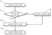
도 5는 본 발명의 일 실시예에 따른 데이터입출력방법의 순서도이다.
도 6은 도 1 내지 도 5에 도시된 반도체장치 및 반도체시스템이 적용된 전자시스템의 일 실시예에 따른 구성을 도시한 도면이다.
도 7은 도 1 내지 도 5에 도시된 반도체장치 및 반도체시스템이 적용된 전자시스템의 다른 실시예에 따른 구성을 도시한 도면이다.1 is a block diagram showing a configuration of a semiconductor system according to an embodiment of the present invention.
2 is a block diagram showing an internal configuration according to an embodiment of a control circuit included in the semiconductor system shown in FIG.
3 is a block diagram illustrating an internal configuration according to an embodiment of the data conversion circuit included in the semiconductor system shown in FIG.
4 is a table for explaining the operation of the latch circuit included in the data conversion circuit shown in Fig.
5 is a flowchart of a data input / output method according to an embodiment of the present invention.
FIG. 6 is a diagram illustrating a configuration according to an embodiment of an electronic system to which the semiconductor device and the semiconductor system shown in FIGS. 1 to 5 are applied.
7 is a diagram showing a configuration according to another embodiment of the electronic system to which the semiconductor device and the semiconductor system shown in Figs. 1 to 5 are applied.
이하, 실시예를 통하여 본 발명을 더욱 상세히 설명하기로 한다. 이들 실시예는 단지 본 발명을 예시하기 위한 것이며, 본 발명의 권리 보호 범위가 이들 실시예에 의해 제한되는 것은 아니다.Hereinafter, the present invention will be described in more detail with reference to Examples. These embodiments are only for illustrating the present invention, and the scope of rights of the present invention is not limited by these embodiments.
도 1에 도시된 바와 같이 본 발명의 일 실시예에 따른 반도체시스템은 제1 반도체장치(1) 및 제2 반도체장치(2)를 포함할 수 있다. 제2 반도체장치(2)는 제어회로(10), 데이터입출력회로(20) 및 메모리영역(30)을 포함할 수 있다. As shown in FIG. 1, a semiconductor system according to an embodiment of the present invention may include a
제1 반도체장치(1)는 제1 내지 제M 커맨드(CMD<1:M>) 및 제1 내지 제N 어드레스(ADD<1:N>)를 출력할 수 있다. 제1 반도체장치(1)는 제1 내지 제4 데이터(DQ<1:4>)를 입출력할 수 있다. 제1 내지 제M 커맨드(CMD<1:M>), 제1 내지 제N 어드레스(ADD<1:N>) 및 제1 내지 제4 데이터(DQ<1:4>)는 어드레스, 커맨드 및 데이터 중 적어도 하나가 전송되는 라인들을 통해 전송될 수 있다. 제1 내지 제M 커맨드(CMD<1:M>) 및 제1 내지 제N 어드레스(ADD<1:N>)의 비트수 M,N은 자연수로 설정될 수 있다. 제1 내지 제4 데이터(DQ<1:4>)의 비트수는 4비트로 설정되어 있지만 실시예에 따라 다양하게 설정될 수 있다. The
제어회로(10)는 제1 내지 제M 커맨드(CMD<1:M>)의 조합에 따라 라이트동작 시 동일한 제1 내지 제N 어드레스(ADD<1:N>)의 조합이 기 설정횟수 이상 입력되는 경우 제어신호(WCTR) 및 제1 및 제2 시프팅신호(SFT<1:2>)를 생성할 수 있다. 제어회로(10)는 제1 내지 제M 커맨드(CMD<1:M>)의 조합에 따라 라이트동작 시 동일한 제1 내지 제N 어드레스(ADD<1:N>)의 조합이 기 설정횟수 이상 입력되는 경우 발생하는 펄스를 포함하는 제어신호(WCTR)를 생성할 수 있다. 제어회로(10)는 제1 내지 제M 커맨드(CMD<1:M>)의 조합에 따라 라이트동작 시 동일한 제1 내지 제N 어드레스(ADD<1:N>)의 조합이 기 설정횟수 이상 입력되는 경우 카운팅되는 제1 및 제2 시프팅신호(SFT<1:2>)를 생성할 수 있다. 제1 및 제2 시프팅신호(SFT<1:2>)의 비트수는 2비트로 설정되어 있지만 실시예 따라 다양한 비트수로 설정될 수 있다. The
데이터입출력회로(20)는 에러정정회로(21) 및 데이터변환회로(22)를 포함할 수 있다. The data input /
에러정정회로(21)는 라이트동작 시 제1 내지 제4 데이터(DQ<1:4>)의 불량을 검출하고, 제1 내지 제4 데이터(DQ<1:4>)의 불량을 정정하여 제1 내지 제4 정정데이터(ECD<1:4>)를 생성할 수 있다. 에러정정회로(21)는 라이트동작 시 제1 내지 제4 데이터(DQ<1:4>)의 불량정보를 포함하는 제1 및 제2 패리티신호(ECP<1:2>)를 생성할 수 있다. 에러정정회로(21)는 리드동작 시 제1 내지 제6 출력데이터(DO<1:6>)에 포함된 제1 및 제2 패리티신호(ECP<1:2>)에 의해 제1 내지 제4 출력데이터(DO<1:4>)의 불량을 정정하여 제1 내지 제4 데이터(DQ<1:4>)로 출력할 수 있다. 에러정정회로(21)는 일반적인 ECC회로로 구현될 수 있다. 제1 내지 제4 정정데이터(ECD<1:4>) 및 제1 및 제2 패리티신호(ECP<1:2>)의 비트수는 실시예에 따라 다양하게 설정될 수 있다. The
데이터변환회로(22)는 라이트동작 시 제어신호(WCTR)에 의해 제1 내지 제4 정정데이터(ECD<1:4>) 및 제1 및 제2 패리티신호(ECP<1:2>)를 시프팅하여 제1 내지 제8 내부데이터(ID<1:8>)를 생성할 수 있다. 데이터변환회로(22)는 리드동작 시 제1 및 제2 시프팅신호(SFT<1:2>)에 의해 제 내지 제8 내부데이터(ID<1:8>)에 포함된 제1 내지 제4 정정데이터(ECD<1:4>) 및 제1 및 제2 패리티신호(ECP<1:2>)의 위치를 복원하여 제1 내지 제6 출력데이터(DO<1:6>)를 생성할 수 있다. 제1 내지 제8 내부데이터(ID<1:8>)는 제1 내지 제4 정정데이터(ECD<1:4>), 제1 및 제2 패리티신호(ECP<1:2>) 및 제1 및 제2 시프팅신호(SFT<1:2>)를 포함할 수 있다. 데이터변환회로(22)가 제어신호(WCTR)에 의해 제1 내지 제4 정정데이터(ECD<1:4>) 및 제1 및 제2 패리티신호(ECP<1:2>)를 시프팅하여 제1 내지 제8 내부데이터(ID<1:8>)를 생성하는 동작은 후술하는 구성을 통해 구체적으로 설명하도록 한다. 또한, 제1 내지 제8 내부데이터(ID<1:8>)에 포함되는 제1 내지 제4 정정데이터(ECD<1:4>), 제1 및 제2 패리티신호(ECP<1:2>) 및 제1 및 제2 시프팅신호(SFT<1:2>)의 위치는 후술하는 구성을 통해 구체적으로 설명하도록 한다. The
즉, 데이터입출력회로(20)는 라이트동작 시 제어신호(WCTR)의 펄스에 응답하여 제1 내지 제4 데이터(DQ<1:4>) 및 불량정보를 시프팅하여 제1 내지 제8 내부데이터(ID<1:8>)를 생성할 수 있다. 데이터입출력회로(20)는 리드동작 시 제1 및 제2 시프팅신호(SFT<1:2>)에 의해 제1 내지 제8 내부데이터(ID<1:8>)에 포함된 제1 내지 제4 데이터(DQ<1:4>) 및 불량정보의 위치를 복원하고, 불량정보에 의해 제1 내지 제8 내부데이터(ID<1:8>)의 불량을 정정하여 제1 내지 제4 데이터(DQ<1:4>)로 출력할 수 있다. 불량정보는 앞서 설명한 제1 및 제2 패리티신호(ECP<1:2>)로 설정될 수 있다. That is, the data input /
메모리영역(30)은 라이트동작 시 제1 내지 제N 어드레스(ADD<1:N>)의 조합에 따라 선택되는 페이지에 제1 내지 제8 내부데이터(ID<1:8>)를 저장할 수 있다. 메모리영역(30)은 리드동작 시 제1 내지 제N 어드레스(ADD<1:N>)의 조합에 따라 선택되는 페이지에 저장된 제1 내지 제8 내부데이터(ID<1:8>)를 출력할 수 있다. 메모리영역(30)은 실시예에 따라 다수의 페이지를 포함하는 비휘발성 메모리장치 또는 다수의 메모리셀어레이를 포함하는 휘발성 메모리장치로 구현될 수 있다. The
이와 같이 구현되는 제2 반도체장치(2)는 제1 내지 제M 커맨드(CMD<1:M>)에 응답하여 라이트동작 시 제1 내지 제4 데이터(DQ<1:4>)의 불량을 정정할 수 있다. 제2 반도체장치(2)는 제1 내지 제N 어드레스(ADD<1:N>)에 따라 선택되는 페이지에 불량이 정정된 제1 내지 제4 데이터(DQ<1:4>) 및 제1 내지 제4 데이터(DQ<1:4>)의 불량정보를 저장할 수 있다. 제2 반도체장치(2)는 제1 내지 제M 커맨드(CMD<1:M>)에 응답하여 라이트동작 시 제1 내지 제N 어드레스(ADD<1:N>)의 동일한 조합이 기 설정된 횟수 이상 입력되는 경우 제1 내지 제4 데이터(DQ<1:4>)와 제1 내지 제4 데이터(DQ<1:4>)의 불량정보를 시프팅하여 페이지에 저장할 수 있다. 제2 반도체장치(2)는 제1 내지 제M 커맨드(CMD<1:M>)에 응답하여 리드동작 시 제1 및 제2 시프팅신호(SFT<1:2>)에 의해 페이지에 저장된 상기 제1 내지 제4 데이터(DQ<1:4>) 및 제1 내지 제4 데이터(DQ<1:4>)의 불량정보의 위치를 복원할 수 있다. 제2 반도체장치(2)는 제1 내지 제M 커맨드(CMD<1:M>)에 응답하여 리드동작 시 불량정보에 의해 제1 내지 제4 데이터(DQ<1:4>)의 불량을 정정하여 출력할 수 있다. The
도 2를 참고하면, 본 발명의 일 실시예에 따른 제어회로(10)는 카운터(11), 제어신호생성회로(12) 및 시프팅신호생성회로(13)를 포함할 수 있다. 2, the
카운터(11)는 제1 내지 제N 어드레스(ADD<1:N>)가 동일한 조합으로 입력되는 경우 카운팅되는 제1 내지 제3 카운팅신호(CNT<1:3>)를 생성할 수 있다. 카운터(11)는 하나의 회로도 도시되어 있지만 페이지의 수에 따라 다수의 카운터로 구현되어 다양한 제1 내지 제N 어드레스(ADD<1:N>) 조합의 동일성을 판단할 수 있다. 제1 내지 제3 카운팅신호(CNT<1:3>)의 비트수는 3비트로 설정되어 있지만 실시예에 따라 다양한 비트수로 설정될 수 있다. The
좀 더 구체적으로 카운터(11)의 동작을 설명하되 동일한 조합의 제1 내지 제N 어드레스(ADD<1:N>)가 4회 입력되는 경우를 예를 들어 설명하면 다음과 같다. More specifically, the operation of the
카운터(11)는 동일한 조합의 제1 내지 제N 어드레스(ADD<1:N>)가 4회 입력되는 경우 모든 비트가 로직로우레벨(L)인 제1 내지 제3 카운팅신호(CNT<1:3>)를 업 카운팅하여 로직로우레벨(L)의 제1 카운팅신호(CNT<1>), 로직로우레벨(L)의 제2 카운팅신호(CNT<2>) 및 로직하이레벨(H)의 제3 카운팅신호(CNT<3>)를 생성할 수 있다. 카운터(11)는 실시예에 따라 동일한 조합의 제1 내지 제N 어드레스(ADD<1:N>)가 입력될 때마다 업카운팅되거나 다운카운팅되는 제1 내지 제3 카운팅신호(CNT<1:3>)를 생성하는 일반적인 카운터로 구현될 수 있다. The
제어신호생성회로(12)는 제1 내지 제M 커맨드(CMD<1:M>)에 따라 라이트동작 시 제1 내지 제3 카운팅신호(CNT<1:3>)가 기 설정된 횟수이상 카운팅되는 경우 발생하는 펄스를 포함하는 제어신호(WCTR)를 생성할 수 있다. The control
좀 더 구체적으로 제어신호생성회로(12)는 제1 내지 제3 카운팅신호(CNT<1:3>)가 4회 카운팅되는 경우 발생하는 펄스를 포함하는 제어신호(WCTR)를 생성할 수 있다. 또한, 제어신호생성회로(12)는 제1 내지 제3 카운팅신호(CNT<1:3>)가 4회 이상 업 카운팅 될 때마다 발생하는 펄스를 포함하는 제어신호(WCTR)를 생성할 수 있다. 즉, 제어신호생성회로(12)는 제1 내지 제3 카운팅신호(CNT<1:3>)가 4회 카운팅되는 경우부터 제1 내지 제3 카운팅신호(CNT<1:3>)가 7회 카운팅되는 경우까지 발생하는 펄스를 포함하는 제어신호(WCTR)를 생성할 수 있다.More specifically, the control
시프팅신호생성회로(13)는 제1 내지 제3 카운팅신호(CNT<1:3>)가 기 설정된 횟수이상 카운팅되는 경우 카운팅되는 제1 및 제2 시프팅신호(SFT<1:2>)를 생성할 수 있다. 제1 및 제2 시프팅신호(SFT<1:2>)는 제1 내지 제4 정정데이터(ECD<1:4>) 및 제1 및 제2 패리티신호(ECP<1:2>)의 시프팅 정보를 포함할 수 있다. The shifting
좀 더 구체적으로 시프팅신호생성회로(13)는 제1 내지 제3 카운팅신호(CNT<1:3>)가 4회 카운팅되는 경우부터 순차적으로 업 카운팅되는 제1 및 제2 시프팅신호(SFT<1:2>)를 생성할 수 있다. 시프팅신호생성회로(13)는 제1 내지 제3 카운팅신호(CNT<1:3>)가 4회 이상 업 카운팅되는 경우부터 제1 내지 제3 카운팅신호(CNT<1:3>)가 7회 카운팅되는 경우까지 업 카운팅되는 제1 및 제2 시프팅신호(SFT<1:2>)를 생성할 수 있다. More specifically, the shifting
예를 들어, 제1 내지 제3 카운팅신호(CNT<1:3>)가 4회 카운팅되는 경우 시프팅신호생성회로(13)는 로직로우레벨(L)의 제1 시프팅신호(SFT<1>) 및 로직로우레벨(L)의 제2 시프팅신호(SFT<2>)를 생성한다. 제1 내지 제3 카운팅신호(CNT<1:3>)가 7회 카운팅되는 경우 시프팅신호생성회로(13)는 로직하이레벨(H)의 제1 시프팅신호(SFT<1>) 및 로직하이레벨(H)의 제2 시프팅신호(SFT<2>)를 생성한다. For example, when the first to third counting signals CNT <1: 3> are counted four times, the shifting
도 3을 참고하면 본 발명의 일 실시예에 따른 데이터변환회로(22)는 래치회로(221) 및 레지스터(222)를 포함할 수 있다. Referring to FIG. 3, the
래치회로(221)는 제어신호(WCTR)의 펄스에 응답하여 제1 내지 제4 정정데이터(ECP<1:4>)와 제1 및 제2 패리티신호(ECP<1:2>)를 시프팅할 수 있다. 래치회로(221)는 시프팅 된 제1 내지 제4 정정데이터(ECP<1:4>)와 제1 및 제2 패리티신호(ECP<1:2>) 및 제1 및 제2 시프팅신호(SFT<1:2>)를 제1 내지 제8 래치데이터(LD<1:8>)로 출력할 수 있다. The
레지스터(222)는 라이트동작 시 입력되는 라이트신호(WT)에 응답하여 제1 내지 제8 래치데이터(LD<1:8>)를 제1 내지 제8 내부데이터(ID<1:8>)로 출력할 수 있다. 레지스터(222)는 리드동작 시 입력되는 리드신호(RD)에 응답하여 제1 내지 제8 내부데이터(ID<1:8>)를 제1 내지 제8 래치데이터(LD<1:8>)로 출력할 수 있다. The
좀 더 구체적으로 도 4를 참고하여 본 발명의 일 실시예에 따른 래치회로(221)에서 생성되는 제1 내지 제8 래치데이터(LD<1:8>)를 구체적으로 살펴보면 다음과 같다. More specifically, the first to eighth latch data LD <1: 8> generated in the
우선, 제어신호(WCTR)가 0회 입력되는 경우 제1 래치데이터(LD<1>)는 제1 정정데이터(ECD<1>)이고, 제2 래치데이터(LD<2>)는 제2 정정데이터(ECD<2>)이며, 제3 래치데이터(LD<3>)는 제3 정정데이터(ECD<3>)이고, 제4 래치데이터(LD<4>)는 제4 정정데이터(ECD<4>)이며, 제5 래치데이터(LD<5>)는 제1 패리티신호(ECP<1>)이고, 제6 래치데이터(LD<6>)는 제2 패리티신호(ECP<2>)이며, 제7 래치데이터(LD<7>)는 제1 시프팅신호(SFT<1>)이고, 제8 래치데이터(LD<8>)는 제2 시프팅신호(SFT<2>)이다. 여기서, 제어신호(WCTR)가 0회 입력되는 경우는 제1 내지 제4 정정데이터(ECP<1:4>)와 제1 및 제2 패리티신호(ECP<1:2>)가 시프팅되지 않는 경우이다. First, when the control signal WCTR is input 0 times, the first latch data LD <1> is the first correction data ECD <1> and the second latch data LD <2> The third latch data LD <3> is the third correction data ECD <3> and the fourth latch data LD <4> is the fourth correction data ECD < 4>), the fifth latch data LD <5> is the first parity signal ECP <1>, the sixth latch data LD <6> is the second parity signal ECP <2> , The seventh latch data LD <7> is the first shifting signal SFT <1>, and the eighth latch data LD <8> is the second shifting signal SFT <2>. Here, when the control signal WCTR is input 0 times, the first to fourth correction data ECP <1: 4> and the first and second parity signals ECP <1: 2> are not shifted .
다음으로, 제어신호(WCTR)가 1회 입력되는 경우 제1 래치데이터(LD<1>)는 제2 패리티신호(ECP<2>)이고, 제2 래치데이터(LD<2>)는 제1 정정데이터(ECD<1>)이며, 제3 래치데이터(LD<3>)는 제2 정정데이터(ECD<2>)이고, 제4 래치데이터(LD<4>)는 제3 정정데이터(ECD<3>)이며, 제5 래치데이터(LD<5>)는 제4 정정데이터(ECD<4>)이고, 제6 래치데이터(LD<6>)는 제1 패리티신호(ECP<1>)이며, 제7 래치데이터(LD<7>)는 제1 시프팅신호(SFT<1>)이고, 제8 래치데이터(LD<8>)는 제2 시프팅신호(SFT<2>)이다. 여기서, 제어신호(WCTR)가 1회 입력되는 경우는 제1 내지 제4 정정데이터(ECP<1:4>)와 제1 및 제2 패리티신호(ECP<1:2>)가 1회 시프팅되는 경우이다. Next, when the control signal WCTR is input once, the first latch data LD <1> is the second parity signal ECP <2> and the second latch data LD <2> 4) is the correction data (ECD <1>), the third latch data LD <3> is the second correction data (ECD <2> 3), the fifth latch data LD <5> is the fourth correction data ECD <4>, the sixth latch data LD <6> is the first parity signal ECP < , The seventh latch data LD <7> is the first shifting signal SFT <1>, and the eighth latch data LD <8> is the second shifting signal SFT <2>. Here, when the control signal WCTR is input once, the first to fourth correction data ECP <1: 4> and the first and second parity signals ECP <1: 2> .
다음으로, 제어신호(WCTR)가 2회 입력되는 경우 제1 래치데이터(LD<1>)는 제1 패리티신호(ECP<1>)이고, 제2 래치데이터(LD<2>)는 제2 패리티신호(ECP<2>)이며, 제3 래치데이터(LD<3>)는 제1 정정데이터(ECD<1>)이고, 제4 래치데이터(LD<4>)는 제2 정정데이터(ECD<2>)이며, 제5 래치데이터(LD<5>)는 제3 정정데이터(ECD<3>)이고, 제6 래치데이터(LD<6>)는 제4 정정데이터(ECD<4>)이며, 제7 래치데이터(LD<7>)는 제1 시프팅신호(SFT<1>)이고, 제8 래치데이터(LD<8>)는 제2 시프팅신호(SFT<2>)이다. 여기서, 제어신호(WCTR)가 2회 입력되는 경우는 제1 내지 제4 정정데이터(ECP<1:4>)와 제1 및 제2 패리티신호(ECP<1:2>)가 2회 시프팅되는 경우이다. Next, when the control signal WCTR is input twice, the first latch data LD <1> is the first parity signal ECP <1> and the second latch data LD <2> 4) is the parity signal ECP <2>, the third latch data LD <3> is the first correction data ECD <1> and the fourth latch data LD <4> 4), the fifth latch data LD <5> is the third correction data ECD <3>, the sixth latch data LD <6> is the fourth correction data ECD < , The seventh latch data LD <7> is the first shifting signal SFT <1>, and the eighth latch data LD <8> is the second shifting signal SFT <2>. Here, when the control signal WCTR is input twice, the first to fourth correction data ECP <1: 4> and the first and second parity signals ECP <1: 2> .
다음으로, 제어신호(WCTR)가 3회 입력되는 경우 제1 래치데이터(LD<1>)는 제4 정정데이터(ECD<4>)이고, 제2 래치데이터(LD<2>)는 제1 패리티신호(ECP<1>)이며, 제3 래치데이터(LD<3>)는 제2 패리티신호(ECP<2>)이고, 제4 래치데이터(LD<4>)는 제1 정정데이터(ECD<1>)이며, 제5 래치데이터(LD<5>)는 제2 정정데이터(ECD<2>)이고, 제6 래치데이터(LD<6>)는 제3 정정데이터(ECD<3>)이며, 제7 래치데이터(LD<7>)는 제1 시프팅신호(SFT<1>)이고, 제8 래치데이터(LD<8>)는 제2 시프팅신호(SFT<2>)이다. 여기서, 제어신호(WCTR)가 3회 입력되는 경우는 제1 내지 제4 정정데이터(ECP<1:4>)와 제1 및 제2 패리티신호(ECP<1:2>)가 3회 시프팅되는 경우이다. Next, when the control signal WCTR is input three times, the first latch data LD <1> is the fourth corrected data ECD <4> and the second latch data LD <2> 4) is the parity signal ECP <1>, the third latch data LD <3> is the second parity signal ECP <2> and the fourth latch data LD <4> 3), the fifth latch data LD <5> is the second correction data ECD <2>, the sixth latch data LD <6> is the third correction data ECD < , The seventh latch data LD <7> is the first shifting signal SFT <1>, and the eighth latch data LD <8> is the second shifting signal SFT <2>. Here, when the control signal WCTR is input three times, the first to fourth correction data ECP <1: 4> and the first and second parity signals ECP <1: 2> .
다음으로, 제어신호(WCTR)가 4회 입력되는 경우 제1 래치데이터(LD<1>)는 제3 정정데이터(ECD<3>)이고, 제2 래치데이터(LD<2>)는 제4 정정데이터(ECD<4>)이며, 제3 래치데이터(LD<3>)는 제1 패리티신호(ECP<1>)이고, 제4 래치데이터(LD<4>)는 제2 패리티신호(ECP<2>)이며, 제5 래치데이터(LD<5>)는 제1 정정데이터(ECD<1>)이고, 제6 래치데이터(LD<6>)는 제2 정정데이터(ECD<2>)이며, 제7 래치데이터(LD<7>)는 제1 시프팅신호(SFT<1>)이고, 제8 래치데이터(LD<8>)는 제2 시프팅신호(SFT<2>)이다. 여기서, 제어신호(WCTR)가 4회 입력되는 경우는 제1 내지 제4 정정데이터(ECP<1:4>)와 제1 및 제2 패리티신호(ECP<1:2>)가 4회 시프팅되는 경우이다. Next, when the control signal WCTR is input four times, the first latch data LD <1> is the third correction data ECD <3> and the second latch data LD <2> The third latch data LD <3> is the first parity signal ECP <1>, the fourth latch data LD <4> is the second parity signal ECP < 2), the fifth latch data LD <5> is the first correction data ECD <1>, the sixth latch data LD <6> is the second correction data ECD < , The seventh latch data LD <7> is the first shifting signal SFT <1>, and the eighth latch data LD <8> is the second shifting signal SFT <2>. Here, when the control signal WCTR is input four times, the first to fourth correction data ECP <1: 4> and the first and second parity signals ECP <1: 2> are shifted four times .
이와 같이 본 발명의 래치회로(221)는 제어신호(WCTR)의 펄스가 입력될 때마다 제1 내지 제4 정정데이터(ECP<1:4>)와 제1 및 제2 패리티신호(ECP<1:2>)를 하나씩 시프팅하여 제1 내지 제6 래치데이터(LD<1:6>)로 출력하고, 제1 및 제2 시프팅신호(SFT<1:2>)를 제7 및 제8 래치데이터(LD<7:6>)로 출력한다. The
도 5를 참고하여 본 발명의 일 실시예에 따른 반도체시스템의 데이터입출력방법을 설명하되, 라이트동작 시 동일한 제1 내지 제N 어드레스(ADD<1:N>)가 4회 입력되는 경우가 기 설정횟수로 설정되고 제1 내지 제N 어드레스(ADD<1:N>)가 5회 입력되는 경우를 예를 들어 설명하면 다음과 같다. A data input / output method of a semiconductor system according to an embodiment of the present invention will be described with reference to FIG. 5. In the case where the same first to Nth addresses ADD <1: N> are input four times during a write operation, And the first to Nth addresses ADD < 1: N > are input five times.
우선, 라이트진입단계(S1)에 진입하면 제1 반도체장치(1)는 라이트동작에 진입하기 위한 제1 내지 제M 커맨드(CMD<1:M>) 및 제1 내지 제N 어드레스(ADD<1:N>)를 출력한다. 이때, 제1 내지 제N 어드레스(ADD<1:N>)는 동한한 조합으로 5회 출력되는 경우이다. First, when the
다음으로, 라이트횟수감지단계(S2)에 진입하면 제어회로(10)의 카운터(11)는 동일한 제1 내지 제N 어드레스(ADD<1:N>)가 5회 입력되므로 제1 내지 제3 카운팅신호(CNT<1:3>)를 5회 업 카운팅하여 로직하이레벨의 제1 카운팅신호(CNT<1>), 로직로우레벨의 제2 카운팅신호(CNT<2>) 및 로직하이레벨의 제3 카운팅신호(CNT<3>)를 생성한다. Next, when entering the write count sensing step S2, the
제어회로(10)의 제어신호생성회로(12)는 제1 내지 제M 커맨드(CMD<1:M>)에 응답하여 제1 내지 제3 카운팅신호(CNT<1:3>)가 기 설정횟수 카운팅되는 4회 업카운팅되는 시점에 제어신호(WCTR)의 펄스를 생성하고, 제1 내지 제3 카운팅신호(CNT<1:3>)가 5회 업카운팅되는 시점에 제어신호(WCTR)의 펄스를 생성한다. 즉, 제어신호(WCTR)의 펄스가 2회 생성된다. The control
제어회로(10)의 시프팅신호생성회로(13)는 제1 내지 제3 카운팅신호(CNT<1:3>)가 5회 업카운팅되는 시점에 제1 및 제2 시프팅신호(SFT<1:2>)를 업카운팅하여 로직하이레벨의 제1 시프팅신호(SFT<1>) 및 로직로우레벨의 제2 시프팅신호(SFT<2>)를 생성한다. The shifting
에러정정회로(21)는 제1 내지 제4 데이터(DQ<1:4>)의 불량을 검출하고, 제1 내지 제4 데이터(DQ<1:4>)의 불량을 정정하여 제1 내지 제4 정정데이터(ECD<1:4>)를 생성하며, 제1 내지 제4 데이터(DQ<1:4>)의 불량정보를 포함하는 제1 및 제2 패리티신호(ECP<1:2>)를 생성한다. The
다음으로, 데이터변환단계(S3)에 진입하여 데이터변환회로(22)의 래치회로(221)는 제어신호(WCTR)의 펄스가 2회 입력되므로 제1 패리티신호(ECP<1>)를 제1 래치데이터(LD<1>)로 출력하고, 제2 패리티신호(ECP<2>)를 제2 래치데이터(LD<2>)로 출력하며, 제1 정정데이터(ECD<1>)를 제3 래치데이터(LD<3>)로 출력하고, 제2 정정데이터(ECD<2>)를 제4 래치데이터(LD<4>)로 출력하며, 제3 정정데이터(ECD<3>)를 제5 래치데이터(LD<5>)로 출력하고, 제4 정정데이터(ECD<4>)를 제6 래치데이터(LD<6>)로 출력하며, 제1 시프팅신호(SFT<1>)를 제7 래치데이터(LD<7>)로 출력하고, 제2 시프팅신호(SFT<2>)를 제8 래치데이터(LD<8>)로 출력한다. Next, since the
즉, 앞서 도 4에서 설명한 바와 같이 제1 내지 제6 래치데이터(LD<1:6>)는 제1 내지 제4 정정데이터(ECD<1:4>) 및 제1 및 제2 패리티신호(ECP<1:2>)를 2회 시프팅하여 생성되고, 제7 및 제8 래치데이터(LD<1:2>)는 제1 및 제2 시프팅신호(SFT<1:2>)로 생성된다. That is, the first to sixth latch data LD <1: 6> are divided into the first to fourth corrected data ECD <1: 4> and the first and second parity signals
다음으로, 라이트동작단계(S4)에 진입하여 데이터변환회로(22)의 레지스터(222)는 라이트신호(WT)에 응답하여 제1 내지 제8 래치데이터(LD<1:8>)를 제1 내지 제8 내부데이터(ID<1:8>)로 출력한다. Next, the write operation step S4 is entered and the
메모리영역(30)은 제1 내지 제N 어드레스(ADD<1:N>)에 의해 선택되는 페이지에 제1 내지 제8 내부데이터(ID<1:8>)를 저장한다. The
다음으로, 라이트종료단계(S5)에 진입하여 라이트동작이 종료된다. Next, the write end step (S5) is entered and the write operation is ended.
이와 같이 구성된 본 발명의 일 실시예에 따른 반도체시스템은 동일한 위치의 페이지를 설정횟수 이상 선택하여 데이터 및 패리티신호를 저장하는 경우 데이터 및 패리티신호의 저장위치를 시프팅하여 저장함으로써 패리티신호의 신뢰성을 확보할 수 있다. 또한, 데이터 및 패리티신호의 저장위치를 시프팅하여 저장함으로써 데이터보다 비트변화가 빈번히 발생하는 패리티신호가 저장되는 영역의 열화를 방지할 수 있다. When the data and parity signals are stored by selecting the page at the same position more than the preset number of times, the semiconductor system according to the embodiment of the present invention configured as described above shifts and stores the storage positions of the data and the parity signals, . In addition, it is possible to prevent deterioration of a region where a parity signal in which a bit change occurs more frequently than data is stored, by shifting and storing the storage positions of data and parity signals.
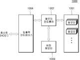
앞서, 도 1 내지 도 5에서 살펴본 반도체장치 및 반도체시스템은 메모리시스템, 그래픽시스템, 컴퓨팅시스템 및 모바일시스템 등을 포함하는 전자시스템에 적용될 수 있다. 예를 들어, 도 6을 참고하면 본 발명의 일 실시예에 따른 전자시스템(1000)은 데이터저장부(1001), 메모리컨트롤러(1002), 버퍼메모리(1003) 및 입출력인터페이스(1004)를 포함할 수 있다.1 to 5 can be applied to an electronic system including a memory system, a graphics system, a computing system, and a mobile system. 6, an
데이터저장부(1001)는 메모리컨트롤러(1002)로부터의 제어신호에 따라 메모리컨트롤러(1002)로부터 인가되는 데이터를 저장하고 저장된 데이터를 판독하여 메모리컨트롤러(1002)에 출력한다. 데이터저장부(1001)는 도 1에 도시된 제2 반도체장치(2)를 포함할 수 있다. 한편, 데이터저장부(1001)는 전원이 차단되어도 데이터를 잃지 않고 계속 저장할 수 있는 비휘발성 메모리를 포함할 수 있다. 비휘발성 메모리는 플래쉬 메모리(Nor Flash Memory, NAND Flash Memory), 상변환 메모리(Phase Change Random Access Memory; PRAM), 저항 메모리(Resistive Random Access Memory;RRAM), 스핀 주입자화반전 메모리(Spin Transfer Torque Random Access Memory; STTRAM), 자기메모리(Magnetic Random Access Memory; MRAM)로 구현될 수 있다.The
메모리컨트롤러(1002)는 입출력인터페이스(1004)를 통해 외부기기(호스트 장치)로부터 인가되는 명령어를 디코딩하고 디코딩된 결과에 따라 데이터저장부(1001) 및 버퍼메모리(1003)에 대한 데이터 입출력을 제어한다. 메모리컨트롤러(1002)는 도 1에 도시된 제1 반도체장치(1)를 포함할 수 있다. 도 6에서는 메모리컨트롤러(1002)가 하나의 블록으로 표시되었으나, 메모리컨트롤러(1002)는 비휘발성 메모리를 제어하기 위한 컨트롤러와 휘발성 메모리인 버퍼메모리(1003)를 제어하기 위한 컨트롤러가 독립적으로 구성될 수 있다.The
버퍼메모리(1003)는 메모리컨트롤러(1002)에서 처리할 데이터 즉 데이터저장부(1001)에 입출력되는 데이터를 임시적으로 저장할 수 있다. 버퍼메모리(1003)는 제어신호에 따라 메모리컨트롤러(1002)에서 인가되는 데이터를 저장할 수 있다. 버퍼메모리(1003)는 저장된 데이터를 판독하여 메모리컨트롤러(1002)에 출력한다. 버퍼메모리(1003)는 DRAM(Dynamic Random Access Memory), Mobile DRAM, SRAM(Static Random Access Memory) 등의 휘발성 메모리를 포함할 수 있다.The
입출력인터페이스(1004)는 메모리컨트롤러(1002)와 외부기기(호스트) 사이의 물리적 연결을 제공하여 메모리컨트롤러(1002)가 외부기기로부터 데이터 입출력을 위한 제어신호를 수신하고 외부기기와 데이터를 교환할 수 있도록 해준다. 입출력인터페이스(1004)는 USB, MMC, PCI-E, SAS, SATA, PATA, SCSI, ESDI, 및 IDE 등과 같은 다양한 인터페이스 프로토콜들 중 하나를 포함할 수 있다.The input /
전자시스템(1000)은 호스트 장치의 보조 기억장치 또는 외부 저장장치로 사용될 수 있다. 전자시스템(1000)은 고상 디스크(Solid State Disk; SSD), USB 메모리(Universal Serial Bus Memory), 씨큐어 디지털 카드(Secure Digital; SD), 미니 씨큐어 디지털 카드(mini Secure Digital card; mSD), 마이크로 씨큐어 디지털 카드(micro SD), 고용량 씨큐어 디지털 카드(Secure Digital High Capacity; SDHC), 메모리 스틱 카드(Memory Stick Card), 스마트 미디어 카드(Smart Media Card; SM), 멀티 미디어 카드(Multi Media Card; MMC), 내장 멀티 미디어 카드(Embedded MMC; eMMC), 컴팩트 플래시 카드(Compact Flash; CF) 등을 포함할 수 있다.The
도 7을 참고하면 본 발명의 다른 실시예에 따른 전자시스템(2000)은 호스트(2001), 메모리컨트롤러(2002) 및 데이터저장부(2003)를 포함할 수 있다.Referring to FIG. 7, an
호스트(2001)는 데이터저장부(2003)를 억세스 하기 위해 메모리컨트롤러(2002)로 리퀘스트 및 데이터를 전송할 수 있다. 메모리컨트롤러(2002)는 리퀘스트에 응답하여 데이터, 데이터 스트로브, 커맨드, 어드레스 및 클럭 등을 데이터저장부(2003)에 제공하고, 이에 응답하여 데이터저장부(2003)는 라이트 또는 리드 동작을 수행하게 할 수 있다. 호스트(2001)는 데이터저장부(2003)로 데이터를 저장시키기 위해 데이터를 메모리컨트롤러(2002)로 전송할 수 있다. 또한 호스트는 데이터저장부(2003)로부터 출력된 데이터를 메모리컨트롤러(2002)를 통해 수신할 수 있다. 호스트(2001)는 오류정정코드(Error Correction Code, ECC) 방식을 사용하여 데이터에 포함된 에러를 정정하는 회로를 포함할 수 있다.The
메모리컨트롤러(2002)는 호스트(2001)와 데이터저장부(2003) 사이의 통신을 중계할 수 있다. 메모리컨트롤러(2002)는 호스트(2001)로부터 리퀘스트와 데이터를 수신하고, 데이터저장부(2003)의 동작을 제어하기 위하여 데이터, 데이터 스트로브, 커맨드, 어드레스 및 클럭 등을 생성하여 데이터저장부(2003)로 제공할 수 있다. 또한, 메모리컨트롤러(2002)는 데이터저장부(2003)로부터 출력된 데이터를 호스트(2001)로 제공할 수 있다.The
데이터저장부(2003)는 다수의 메모리들을 포함할 수 있다. 데이터저장부(2003)는 메모리컨트롤러(2002)로부터 데이터, 데이터 스트로브, 커맨드, 어드레스 및 클럭 등을 수신하여 라이트 또는 리드 동작을 수행할 수 있다. 데이터저장부(2003)에 포함된 다수의 메모리들은 오류정정코드(Error Correction Code, ECC) 방식을 사용하여 데이터에 포함된 에러를 정정하는 회로를 포함할 수 있다.The
호스트(2001)에 포함된 에러를 정정하는 회로 및 데이터저장부(2003) 내부의 다수의 메모리들에 포함된 에러를 정정하는 회로는 실시예에 따라서 모두 동작하거나 선택적으로 동작하도록 구현될 수 있다. 호스트(2001) 및 메모리컨트롤러(2002)는 실시예에 따라서 동일한 칩으로 구현될 수 있다. 메모리컨트롤러(2002) 및 데이터저장부(2003)는 실시예에 따라서 동일한 칩으로 구현될 수 있다. Circuitry for correcting errors contained in the
1. 제1 반도체장치
2. 제2 반도체장치
10. 제어회로
11. 카운터
12. 제어신호생성회로
13. 시프팅신호생성회로
20. 데이터입출력회로
21. 에러정정회로
22. 데이터변환회로
30. 메모리영역
221. 래치회로
222. 레지스터1.
10.
12. Control
20. Data I /
22.
221.
Claims (25)
상기 커맨드에 응답하여 라이트동작에 진입하고, 상기 데이터의 불량을 정정하며, 상기 어드레스에 따라 선택되는 페이지에 불량이 정정된 상기 데이터 및 상기 데이터의 불량정보를 저장하되, 상기 어드레스의 동일한 조합이 기 설정된 횟수 이상 입력되는 경우 상기 데이터와 상기 데이터의 불량정보를 시프팅하여 상기 페이지에 저장하는 제2 반도체장치를 포함하는 반도체시스템.
A first semiconductor device which outputs a command and an address and inputs and outputs data; And
Storing the data whose defect is corrected on a page selected in accordance with the address and the defect information of the data, wherein the same combination of the addresses is stored in the page And a second semiconductor device for shifting the data and the defective information of the data when the data is inputted more than the set number of times, and storing the shifted data in the page.
상기 라이트동작 중 상기 동일한 조합의 어드레스가 상기 기 설정된 횟수 미만으로 입력되는 경우 상기 페이지에 저장되는 상기 데이터 및 상기 불량정보를 시프팅하지 않고 저장하는 반도체시스템.
The semiconductor device according to claim 1, wherein the second semiconductor device
And stores the data and the bad information stored in the page without shifting when the same combination address is input less than the predetermined number of times during the writing operation.
리드동작 시 시프팅되어 상기 페이지에 저장된 상기 데이터 및 상기 불량정보의 위치를 복원하고, 상기 불량정보에 의해 상기 데이터의 불량을 정정하여 출력하는 반도체시스템.
The semiconductor device according to claim 1, wherein the second semiconductor device
The data and the position of the defective information stored in the page are shifted during a read operation, and the defect of the data is corrected by the defective information and outputted.
상기 커맨드에 응답하여 상기 라이트동작 시 동일한 상기 어드레스의 조합이 상기 기 설정된 횟수 이상 입력되는 경우 발생하는 펄스를 포함하는 제어신호 및 동일한 상기 어드레스의 조합이 상기 기 설정된 횟수 이상 입력되는 경우 카운팅되는 시프팅신호를 생성하는 제어회로; 및
상기 제어신호의 펄스에 응답하여 상기 데이터 및 상기 불량정보를 시프팅하여 내부데이터를 생성하는 데이터입출력회로를 포함하는 반도체시스템.
The semiconductor device according to claim 1, wherein the second semiconductor device
A control signal including a pulse generated in response to the command when a combination of the same address is input more than the predetermined number of times during the write operation and a control signal including a shift signal when a combination of the same address is input more than the preset number of times A control circuit for generating a signal; And
And a data input / output circuit for shifting the data and the defect information in response to the pulse of the control signal to generate internal data.
5. The semiconductor system according to claim 4, wherein the internal data includes the data, the bad information, and the shifting signal.
리드동작 시 상기 시프팅신호에 의해 상기 내부데이터에 포함된 상기 데이터 및 상기 불량정보의 위치를 복원하고, 상기 불량정보에 의해 상기 내부데이터의 불량을 정정하여 상기 데이터로 출력하는 반도체시스템.
The data input / output circuit according to claim 4, wherein the data input /
Restores the data and the position of the defect information included in the internal data by the shifting signal during a read operation, corrects the defect of the internal data by the defect information, and outputs the corrected data.
상기 어드레스가 동일한 조합인 경우 카운팅되는 카운팅신호를 생성하는 카운터;
상기 커맨드에 응답하여 상기 카운팅신호가 상기 기 설정된 횟수이상 카운팅되는 경우 발생하는 펄스를 포함하는 상기 제어신호를 생성하는 제어신호생성회로; 및
상기 카운팅신호가 상기 기 설정된 횟수이상 카운팅되는 경우 카운팅되는 상기 시프팅신호를 생성하는 시프팅신호생성회로를 포함하는 반도체시스템.
5. The apparatus of claim 4, wherein the control circuit
A counter for generating a counting signal counted when the addresses are the same combination;
A control signal generating circuit for generating the control signal including a pulse generated when the counting signal is counted more than the predetermined number of times in response to the command; And
And a shifting signal generating circuit for generating the shifting signal counted when the counting signal is counted more than the preset number of times.
상기 라이트동작 시 상기 데이터의 불량을 검출하고, 상기 데이터의 불량을 정정하여 정정데이터를 생성하며, 상기 데이터의 불량정보를 포함하는 패리티신호를 생성하는 에러정정회로; 및
상기 제어신호에 응답하여 상기 정정데이터 및 상기 패리티신호를 시프팅하여 상기 내부데이터를 생성하는 데이터변환회로를 포함하는 반도체시스템.
The data input / output circuit according to claim 4, wherein the data input /
An error correction circuit for detecting a defect of the data during the write operation, generating a correction data by correcting the data deficiency, and generating a parity signal including defective data of the data; And
And a data conversion circuit for shifting the correction data and the parity signal in response to the control signal to generate the internal data.
상기 에러정정회로는 리드동작 시 상기 패리티신호에 의해 출력데이터의 불량을 정정하여 상기 데이터로 출력하고,
상기 데이터변환회로는 상기 리드동작 시 상기 시프팅신호에 의해 상기 내부데이터에 포함된 상기 정정데이터 및 상기 패리티신호의 위치를 복원하여 상기 출력데이터를 생성하는 반도체시스템.
9. The method of claim 8,
Wherein the error correction circuit corrects a defective output data by the parity signal during a read operation and outputs the corrected data as the data,
Wherein the data conversion circuit restores the position of the correction data and the parity signal included in the internal data by the shifting signal during the read operation to generate the output data.
상기 제어신호의 펄스가 입력되는 횟수만큼 상기 정정데이터와 상기 패리티신호를 시프팅하고, 시프팅 된 상기 정정데이터와 상기 패리티신호 및 상기 시프팅신호를 래치데이터로 출력하는 래치회로; 및
라이트신호에 응답하여 상기 래치데이터를 상기 내부데이터로 출력하는 레지스터를 포함하는 반도체시스템.
The data conversion circuit according to claim 8, wherein the data conversion circuit
A latch circuit for shifting the correction data and the parity signal by a number of times the pulse of the control signal is inputted and outputting the shifted correction data, the parity signal and the shifting signal as latch data; And
And a register for outputting said latch data as said internal data in response to a write signal.
상기 래치회로는 리드동작 시 상기 래치데이터에 포함된 상기 시프팅신호에 의해 상기 정정데이터와 상기 패리티신호의 위치를 복원하여 상기 출력데이터로 출력하고,
상기 레지스터는 리드신호에 응답하여 상기 내부데이터를 상기 래치데이터로 출력하는 반도체시스템.
11. The method of claim 10,
Wherein the latch circuit restores the position of the correction data and the parity signal by the shifting signal included in the latch data during a read operation and outputs the restored data as the output data,
And the register outputs the internal data as the latch data in response to a read signal.
상기 라이트동작 시 상기 어드레스의 조합에 따라 선택되는 상기 페이지에 상기 내부데이터를 저장하고, 상기 리드동작 시 상기 어드레스의 조합에 따라 선택되는 상기 페이지에 저장된 상기 내부데이터를 출력하는 메모리영역을 더 포함하는 반도체시스템.
The semiconductor device according to claim 3, wherein the second semiconductor device
And a memory area for storing the internal data in the page selected in accordance with the combination of the addresses in the write operation and outputting the internal data stored in the page selected in accordance with the combination of the addresses in the read operation Semiconductor system.
상기 제어신호의 펄스에 응답하여 데이터 및 불량정보를 시프팅하여 내부데이터를 생성하는 데이터입출력회로; 및
상기 라이트동작 시 상기 어드레스에 의해 선택되는 페이지에 상기 내부데이터를 저장하고, 리드동작 시 상기 어드레스의 조합에 따라 선택되는 상기 페이지에 저장된 상기 내부데이터를 출력하는 메모리영역을 포함하는 반도체장치.
A control circuit for generating a shifting signal which is counted when a control signal including a pulse generated when a combination of the same address is input in a write operation is inputted a predetermined number of times or more and a combination of the same address is inputted more than the predetermined number of times;
A data input / output circuit for generating internal data by shifting data and defect information in response to the pulse of the control signal; And
And a memory area for storing the internal data in a page selected by the address in the write operation and outputting the internal data stored in the page selected in accordance with the combination of the addresses in a read operation.
상기 제어신호의 펄스가 입력되는 횟수만큼 상기 내부데이터에 저장되는 상기 데이터 및 상기 불량정보를 시프팅하는 반도체장치.
14. The semiconductor memory device according to claim 13, wherein the data input /
And shifting the data and the defect information stored in the internal data by the number of times the pulse of the control signal is input.
14. The semiconductor device according to claim 13, wherein the internal data includes the data, the bad information, and the shifting signal.
상기 리드동작 시 상기 시프팅신호에 의해 상기 내부데이터에 포함된 상기 데이터 및 상기 불량정보의 위치를 복원하고, 상기 불량정보에 의해 상기 내부데이터의 불량을 정정하여 상기 데이터로 출력하는 반도체장치.
14. The semiconductor memory device according to claim 13, wherein the data input /
And restores the position of the data and the defect information included in the internal data by the shifting signal during the read operation, corrects the defect of the internal data by the defect information, and outputs the corrected data.
상기 어드레스가 동일한 조합인 경우 카운팅되는 카운팅신호를 생성하는 카운터;
커맨드에 응답하여 상기 카운팅신호가 상기 기 설정된 횟수이상 카운팅되는 경우 발생하는 펄스를 포함하는 상기 제어신호를 생성하는 제어신호생성회로; 및
상기 카운팅신호가 상기 기 설정된 횟수이상 카운팅되는 경우 카운팅되는 상기 시프팅신호를 생성하는 시프팅신호생성회로를 포함하는 반도체장치.
14. The apparatus of claim 13, wherein the control circuit
A counter for generating a counting signal counted when the addresses are the same combination;
A control signal generation circuit for generating the control signal including a pulse generated when the counting signal is counted more than the predetermined number of times in response to a command; And
And a shifting signal generating circuit for generating the shifting signal counted when the counting signal is counted more than the preset number of times.
상기 라이트동작 시 상기 데이터의 불량을 검출하고, 상기 데이터의 불량을 정정하여 정정데이터를 생성하며, 상기 데이터의 불량정보를 포함하는 패리티신호를 생성하는 에러정정회로; 및
상기 제어신호의 펄스에 응답하여 상기 정정데이터 및 상기 패리티신호를 시프팅하여 상기 내부데이터를 생성하는 데이터변환회로를 포함하는 반도체장치.
14. The semiconductor memory device according to claim 13, wherein the data input /
An error correction circuit for detecting a defect of the data during the write operation, generating a correction data by correcting the data deficiency, and generating a parity signal including defective data of the data; And
And a data conversion circuit that generates the internal data by shifting the correction data and the parity signal in response to the pulse of the control signal.
상기 에러정정회로는 상기 리드동작 시 상기 패리티신호에 의해 출력데이터의 불량을 정정하여 상기 데이터로 출력하고,
상기 데이터변환회로는 상기 리드동작 시 상기 시프팅신호에 의해 상기 내부데이터에 포함된 상기 정정데이터 및 상기 패리티신호의 위치를 복원하여 상기 출력데이터를 생성하는 반도체장치.
19. The method of claim 18,
Wherein the error correction circuit corrects a failure of the output data by the parity signal during the read operation and outputs the corrected data,
Wherein the data conversion circuit restores the position of the correction data and the parity signal included in the internal data by the shifting signal during the read operation to generate the output data.
상기 제어신호의 펄스가 입력되는 횟수만큼 상기 정정데이터와 상기 패리티신호를 시프팅하고, 시프팅 된 상기 정정데이터와 상기 패리티신호 및 상기 시프팅신호를 래치데이터로 출력하는 래치회로; 및
라이트신호에 응답하여 상기 래치데이터를 상기 내부데이터로 출력하는 레지스터를 포함하는 반도체장치.
19. The data conversion circuit according to claim 18, wherein the data conversion circuit
A latch circuit for shifting the correction data and the parity signal by a number of times the pulse of the control signal is inputted and outputting the shifted correction data, the parity signal and the shifting signal as latch data; And
And a register for outputting said latch data as said internal data in response to a write signal.
상기 래치회로는 상기 리드동작 시 상기 래치데이터에 포함된 상기 시프팅신호에 의해 상기 정정데이터와 상기 패리티신호의 위치를 복원하여 상기 출력데이터로 출력하고,
상기 레지스터는 리드신호에 응답하여 상기 내부데이터를 상기 래치데이터로 출력하는 반도체장치.
21. The method of claim 20,
Wherein the latch circuit restores the position of the correction data and the parity signal by the shifting signal included in the latch data during the read operation and outputs the restored data as the output data,
And the register outputs the internal data as the latch data in response to a read signal.
상기 라이트동작 시 동일한 어드레스가 기 설정된 횟수 이상 입력되는 경우를 판단하는 라이트횟수감지단계; 및
상기 동일한 어드레스가 상기 기 설정된 횟수 이상 입력되는 경우 발생하는 펄스를 포함하는 제어신호를 생성하고, 상기 동일한 어드레스가 상기 기 설정된 횟수 이상 입력되는 경우 카운팅되는 시프팅신호를 생성하며, 상기 제어신호에 포함된 펄스의 생성횟수만큼 데이터 및 상기 데이터의 불량정보를 시프팅하여 내부데이터를 생성하는 데이터변환단계를 포함하는 데이터입출력방법.
A light entry step of entering a write operation in response to a command;
A write count sensing step of determining whether the same address is input a predetermined number of times or more in the write operation; And
Generates a control signal including a pulse generated when the same address is inputted more than the predetermined number of times, generates a shifting signal counted when the same address is inputted more than the predetermined number of times, And a data conversion step of shifting the data and the defect information of the data by the number of generation times of the generated pulses to generate internal data.
23. The data input / output method according to claim 22, wherein the internal data includes the data, the bad information, and the shifting signal.
상기 어드레스에 의해 선택되는 페이지에 상기 내부데이터를 저장하는 라이트동작단계를 더 포함하는 데이터입출력방법.
23. The method of claim 22,
And a write operation step of storing the internal data in a page selected by the address.
상기 동일한 어드레스가 상기 기 설정된 횟수 미만으로 입력되는 경우 상기 데이터, 상기 불량정보를 시프팅하지 않고 상기 내부데이터로 저장하는 데이터입출력방법.
25. The method of claim 24, wherein the write operation step
And storing the data and the bad information as the internal data without shifting when the same address is input less than the predetermined number of times.
Priority Applications (4)
| Application Number | Priority Date | Filing Date | Title |
|---|---|---|---|
| KR1020160076051A KR20170143084A (en) | 2016-06-17 | 2016-06-17 | Semiconductor device and semiconductor system |
| US15/439,186 US10360950B2 (en) | 2016-06-17 | 2017-02-22 | Methods, semiconductor devices, and semiconductor systems |
| US16/439,452 US11081150B2 (en) | 2016-06-17 | 2019-06-12 | Methods, semiconductor devices, and semiconductor systems |
| US17/358,309 US11456021B2 (en) | 2016-06-17 | 2021-06-25 | Methods, semiconductor devices, and semiconductor systems |
Applications Claiming Priority (1)
| Application Number | Priority Date | Filing Date | Title |
|---|---|---|---|
| KR1020160076051A KR20170143084A (en) | 2016-06-17 | 2016-06-17 | Semiconductor device and semiconductor system |
Publications (1)
| Publication Number | Publication Date |
|---|---|
| KR20170143084A true KR20170143084A (en) | 2017-12-29 |
Family
ID=60661407
Family Applications (1)
| Application Number | Title | Priority Date | Filing Date |
|---|---|---|---|
| KR1020160076051A KR20170143084A (en) | 2016-06-17 | 2016-06-17 | Semiconductor device and semiconductor system |
Country Status (2)
| Country | Link |
|---|---|
| US (3) | US10360950B2 (en) |
| KR (1) | KR20170143084A (en) |
Cited By (1)
| Publication number | Priority date | Publication date | Assignee | Title |
|---|---|---|---|---|
| KR20180022015A (en) * | 2016-08-23 | 2018-03-06 | 에스케이하이닉스 주식회사 | Semiconductor device for providing method of testing a latch circuit |
Families Citing this family (1)
| Publication number | Priority date | Publication date | Assignee | Title |
|---|---|---|---|---|
| CN109859781B (en) * | 2019-02-25 | 2020-10-27 | 杨忠 | Big data memory with data analysis function |
Family Cites Families (29)
| Publication number | Priority date | Publication date | Assignee | Title |
|---|---|---|---|---|
| KR100515720B1 (en) * | 1998-02-21 | 2005-11-29 | 삼성전자주식회사 | How to Optimize Lead / Light Channel Factors |
| JP3230485B2 (en) * | 1998-04-09 | 2001-11-19 | 日本電気株式会社 | One-chip microcomputer |
| JP2002288988A (en) * | 2001-03-28 | 2002-10-04 | Mitsubishi Electric Corp | Non-volatile semiconductor memory |
| JP2003091923A (en) * | 2001-09-18 | 2003-03-28 | Sony Corp | Re-sampling address generator circuit |
| US6741515B2 (en) * | 2002-06-18 | 2004-05-25 | Nanoamp Solutions, Inc. | DRAM with total self refresh and control circuit |
| JP3910902B2 (en) * | 2002-10-02 | 2007-04-25 | 松下電器産業株式会社 | Integrated circuit device |
| JP4205396B2 (en) * | 2002-10-30 | 2009-01-07 | エルピーダメモリ株式会社 | Semiconductor integrated circuit device |
| JP4135680B2 (en) * | 2004-05-31 | 2008-08-20 | ソニー株式会社 | Semiconductor memory device and signal processing system |
| TWI265093B (en) * | 2005-12-29 | 2006-11-01 | Ind Tech Res Inst | Integrated circuit of inkjet print system and control circuit thereof |
| US7943723B2 (en) * | 2006-12-21 | 2011-05-17 | E. I. Du Pont De Nemours And Company | Process for the synthesis of ethers of aromatic acids |
| US7606070B2 (en) * | 2006-12-29 | 2009-10-20 | Sandisk Corporation | Systems for margined neighbor reading for non-volatile memory read operations including coupling compensation |
| KR101297562B1 (en) * | 2007-02-23 | 2013-08-19 | 삼성전자주식회사 | Early write semiconductor memory device and method of controlling bit line sense amplifier of the same |
| US7477545B2 (en) * | 2007-06-14 | 2009-01-13 | Sandisk Corporation | Systems for programmable chip enable and chip address in semiconductor memory |
| US7715255B2 (en) * | 2007-06-14 | 2010-05-11 | Sandisk Corporation | Programmable chip enable and chip address in semiconductor memory |
| US8060798B2 (en) | 2007-07-19 | 2011-11-15 | Micron Technology, Inc. | Refresh of non-volatile memory cells based on fatigue conditions |
| KR100960479B1 (en) * | 2007-12-24 | 2010-06-01 | 주식회사 하이닉스반도체 | Flash memory apparatus and operating method thereof |
| US8261165B2 (en) * | 2008-11-14 | 2012-09-04 | Silicon Laboratories Inc. | Multi-syndrome error correction circuit |
| JP5282560B2 (en) * | 2008-12-19 | 2013-09-04 | 富士通セミコンダクター株式会社 | Semiconductor device and system |
| US8347175B2 (en) * | 2009-09-28 | 2013-01-01 | Kabushiki Kaisha Toshiba | Magnetic memory |
| JP5388976B2 (en) * | 2010-09-22 | 2014-01-15 | 株式会社東芝 | Semiconductor memory control device |
| US8842473B2 (en) * | 2012-03-15 | 2014-09-23 | Sandisk Technologies Inc. | Techniques for accessing column selecting shift register with skipped entries in non-volatile memories |
| KR101939234B1 (en) * | 2012-07-23 | 2019-01-16 | 삼성전자 주식회사 | Memory device, memory system and method of controlling a read voltage of the memory device |
| US9329948B2 (en) | 2012-09-15 | 2016-05-03 | Seagate Technology Llc | Measuring cell damage for wear leveling in a non-volatile memory |
| US8990670B2 (en) | 2012-09-28 | 2015-03-24 | Intel Corporation | Endurance aware error-correcting code (ECC) protection for non-volatile memories |
| US8773924B2 (en) * | 2012-12-05 | 2014-07-08 | Lsi Corporation | Read assist scheme for reducing read access time in a memory |
| US9280301B2 (en) * | 2013-08-28 | 2016-03-08 | Huawei Technologies Co., Ltd. | Method and device for recovering erroneous data |
| KR102178141B1 (en) * | 2014-08-01 | 2020-11-12 | 삼성전자주식회사 | Method of operating nonvolatile memory device |
| US9653161B2 (en) * | 2014-11-21 | 2017-05-16 | Panasonic Intellectual Property Management Co., Ltd. | Tamper-resistant non-volatile memory device comprising an arithmetic circuit that, in operation, calculates a binary reference value based on at least a part of the pieces of resistance value information, a read circuit that, in operation, selectively assigns, based on the binary reference value, one of two values to each of the pieces of resistance value information, and a write circuit that, in operation, performs a write operation corresponding to one of the two values among memory cells |
| KR102372730B1 (en) * | 2015-08-25 | 2022-03-10 | 삼성전자주식회사 | Non-volatile memory device, operating method thereof and solid state drive including the same |
-
2016
- 2016-06-17 KR KR1020160076051A patent/KR20170143084A/en not_active Application Discontinuation
-
2017
- 2017-02-22 US US15/439,186 patent/US10360950B2/en active Active
-
2019
- 2019-06-12 US US16/439,452 patent/US11081150B2/en active Active
-
2021
- 2021-06-25 US US17/358,309 patent/US11456021B2/en active Active
Cited By (1)
| Publication number | Priority date | Publication date | Assignee | Title |
|---|---|---|---|---|
| KR20180022015A (en) * | 2016-08-23 | 2018-03-06 | 에스케이하이닉스 주식회사 | Semiconductor device for providing method of testing a latch circuit |
Also Published As
| Publication number | Publication date |
|---|---|
| US11456021B2 (en) | 2022-09-27 |
| US10360950B2 (en) | 2019-07-23 |
| US11081150B2 (en) | 2021-08-03 |
| US20210319813A1 (en) | 2021-10-14 |
| US20170365303A1 (en) | 2017-12-21 |
| US20190295611A1 (en) | 2019-09-26 |
Similar Documents
| Publication | Publication Date | Title |
|---|---|---|
| KR20170082066A (en) | Semiconductor system | |
| US10572341B2 (en) | Semiconductor devices | |
| KR102692010B1 (en) | Semiconductor device for executing a test method checking a cell allay failure | |
| US10162703B2 (en) | Methods of correcting data errors and semiconductor devices used therein | |
| US10579472B2 (en) | Semiconductor devices | |
| US10811116B2 (en) | Semiconductor systems | |
| US20170286218A1 (en) | Semiconductor devices, and semiconductor systems | |
| KR20180000594A (en) | Semiconductor device and semiconductor system | |
| KR20180029803A (en) | Semiconductor device and semiconductor system | |
| US11456021B2 (en) | Methods, semiconductor devices, and semiconductor systems | |
| KR20190060258A (en) | Error scrub method and semiconductor module using the same | |
| US10153028B2 (en) | Semiconductor devices | |
| US20180018219A1 (en) | Semiconductor devices and semiconductor systems | |
| US10917111B2 (en) | Error correction code unit and error correction method | |
| US20170344422A1 (en) | Semiconductor devices and semiconductor systems | |
| US10460826B2 (en) | Test methods of semiconductor devices and semiconductor systems used therein | |
| KR20180055148A (en) | Semiconductor device and semiconductor system | |
| US10360105B2 (en) | Semiconductor devices and semiconductor systems including the same | |
| US20170235634A1 (en) | Semiconductor devices and semiconductor systems including the same | |
| KR20180086817A (en) | Semiconductor device | |
| US10014073B2 (en) | Semiconductor devices | |
| CN116069548A (en) | Memory device, memory module, and method of operating memory controller |
Legal Events
| Date | Code | Title | Description |
|---|---|---|---|
| E902 | Notification of reason for refusal | ||
| E601 | Decision to refuse application |