KR20170142714A - Data storage device and operating method thereof - Google Patents
Data storage device and operating method thereof Download PDFInfo
- Publication number
- KR20170142714A KR20170142714A KR1020160076658A KR20160076658A KR20170142714A KR 20170142714 A KR20170142714 A KR 20170142714A KR 1020160076658 A KR1020160076658 A KR 1020160076658A KR 20160076658 A KR20160076658 A KR 20160076658A KR 20170142714 A KR20170142714 A KR 20170142714A
- Authority
- KR
- South Korea
- Prior art keywords
- threshold voltage
- bias
- determining
- read
- read bias
- Prior art date
Links
Images


Classifications
-
- G—PHYSICS
- G11—INFORMATION STORAGE
- G11C—STATIC STORES
- G11C16/00—Erasable programmable read-only memories
- G11C16/02—Erasable programmable read-only memories electrically programmable
- G11C16/06—Auxiliary circuits, e.g. for writing into memory
- G11C16/26—Sensing or reading circuits; Data output circuits
-
- G—PHYSICS
- G11—INFORMATION STORAGE
- G11C—STATIC STORES
- G11C11/00—Digital stores characterised by the use of particular electric or magnetic storage elements; Storage elements therefor
- G11C11/56—Digital stores characterised by the use of particular electric or magnetic storage elements; Storage elements therefor using storage elements with more than two stable states represented by steps, e.g. of voltage, current, phase, frequency
- G11C11/5621—Digital stores characterised by the use of particular electric or magnetic storage elements; Storage elements therefor using storage elements with more than two stable states represented by steps, e.g. of voltage, current, phase, frequency using charge storage in a floating gate
- G11C11/5642—Sensing or reading circuits; Data output circuits
-
- G—PHYSICS
- G06—COMPUTING; CALCULATING OR COUNTING
- G06F—ELECTRIC DIGITAL DATA PROCESSING
- G06F12/00—Accessing, addressing or allocating within memory systems or architectures
- G06F12/02—Addressing or allocation; Relocation
- G06F12/0223—User address space allocation, e.g. contiguous or non contiguous base addressing
- G06F12/023—Free address space management
- G06F12/0238—Memory management in non-volatile memory, e.g. resistive RAM or ferroelectric memory
-
- G—PHYSICS
- G11—INFORMATION STORAGE
- G11C—STATIC STORES
- G11C16/00—Erasable programmable read-only memories
- G11C16/02—Erasable programmable read-only memories electrically programmable
- G11C16/04—Erasable programmable read-only memories electrically programmable using variable threshold transistors, e.g. FAMOS
- G11C16/0483—Erasable programmable read-only memories electrically programmable using variable threshold transistors, e.g. FAMOS comprising cells having several storage transistors connected in series
-
- G—PHYSICS
- G11—INFORMATION STORAGE
- G11C—STATIC STORES
- G11C16/00—Erasable programmable read-only memories
- G11C16/02—Erasable programmable read-only memories electrically programmable
- G11C16/06—Auxiliary circuits, e.g. for writing into memory
- G11C16/26—Sensing or reading circuits; Data output circuits
- G11C16/28—Sensing or reading circuits; Data output circuits using differential sensing or reference cells, e.g. dummy cells
-
- G—PHYSICS
- G11—INFORMATION STORAGE
- G11C—STATIC STORES
- G11C16/00—Erasable programmable read-only memories
- G11C16/02—Erasable programmable read-only memories electrically programmable
- G11C16/06—Auxiliary circuits, e.g. for writing into memory
- G11C16/30—Power supply circuits
-
- G—PHYSICS
- G11—INFORMATION STORAGE
- G11C—STATIC STORES
- G11C2211/00—Indexing scheme relating to digital stores characterized by the use of particular electric or magnetic storage elements; Storage elements therefor
- G11C2211/56—Indexing scheme relating to G11C11/56 and sub-groups for features not covered by these groups
- G11C2211/563—Multilevel memory reading aspects
- G11C2211/5634—Reference cells
Abstract
Description
본 발명은 데이터 저장 장치에 관한 것으로, 더욱 상세하게는 비휘발성 메모리 장치를 포함하는 데이터 저장 장치에 관한 것이다.BACKGROUND OF THE
데이터 저장 장치는 외부 장치의 라이트 요청에 응답하여, 외부 장치로부터 제공된 데이터를 저장하도록 구성될 수 있다. 또한, 데이터 저장 장치는 외부 장치의 리드 요청에 응답하여, 저장된 데이터를 외부 장치로 제공하도록 구성될 수 있다. 외부 장치는 데이터를 처리할 수 있는 전자 장치로서, 컴퓨터, 디지털 카메라 또는 휴대폰 등을 포함할 수 있다. 데이터 저장 장치는 외부 장치에 내장되어 동작하거나, 분리 가능한 형태로 제작되어 외부 장치에 연결됨으로써 동작할 수 있다.The data storage device may be configured to store data provided from an external device in response to a write request of the external device. In addition, the data storage device may be configured to provide stored data to an external device in response to a read request of the external device. An external device is an electronic device capable of processing data, and may include a computer, a digital camera, a cellular phone, or the like. The data storage device may be built in an external device or operated in a detachable form and connected to an external device.
본 발명의 실시 예는 리드 동작의 성능이 향상된 데이터 저장 장치 및 그것의 동작 방법을 제공하는 데 있다.An embodiment of the present invention is to provide a data storage device with improved performance of a read operation and a method of operation thereof.
본 발명의 실시 예에 따른 데이터 저장 장치의 동작 방법은 복수의 메모리 셀들의 문턱 전압 분포들 중 인접한 타겟 문턱 전압 분포들에 대해 제1 리드 바이어스의 적합성을 판단하는 단계 및 판단 결과에 따라 제2 리드 바이어스를 결정하는 단계를 포함할 수 있다.A method of operating a data storage device according to an embodiment of the present invention includes determining a suitability of a first read bias to adjacent target threshold voltage distributions among threshold voltage distributions of a plurality of memory cells, And determining a bias.
본 발명의 실시 예에 따른 데이터 저장 장치의 동작 방법은 복수의 메모리 셀들의 문턱 전압 분포들 중 인접한 타겟 문턱 전압 분포들에 대해 제1 리드 바이어스의 오차율을 산출함으로써 상기 제1 리드 바이어스의 적합성을 판단하는 단계; 판단 결과에 따라 가우시안 모델링 알고리즘 및 상기 오차율에 근거하여 상기 타겟 문턱 전압 분포들에 대응하는 시작 바이어스를 결정하는 단계; 및 상기 시작 바이어스에 근거하여 제2 리드 바이어스를 결정하는 단계를 포함할 수 있다.The method of operating a data storage device according to an embodiment of the present invention determines the suitability of the first read bias by calculating an error rate of a first read bias with respect to adjacent target threshold voltage distributions among threshold voltage distributions of a plurality of memory cells ; Determining a starting bias corresponding to the target threshold voltage distributions based on a Gaussian modeling algorithm and the error rate according to a determination result; And determining a second read bias based on the start bias.
본 발명의 실시 예에 따른 데이터 저장 장치의 동작 방법은 가우시안 모델링 알고리즘 및 제1 리드 바이어스에 근거하여 복수의 메모리 셀들의 문턱 전압 분포들 중 인접한 타겟 문턱 전압 분포들에 대응하는 시작 바이어스를 결정하는 단계; 및 상기 시작 바이어스에 근거하여 상기 타겟 문턱 전압 분포들에 대해 제2 리드 바이어스를 결정하는 단계를 포함할 수 있다.A method of operating a data storage device according to an embodiment of the present invention includes determining a start bias corresponding to adjacent target threshold voltage distributions among threshold voltage distributions of a plurality of memory cells based on a Gaussian modeling algorithm and a first read bias ; And determining a second read bias for the target threshold voltage distributions based on the start bias.
본 발명의 실시 예에 따른 데이터 저장 장치 및 그것의 동작 방법은 성능이 향상된 리드 동작을 수행할 수 있다.A data storage device and an operation method thereof according to an embodiment of the present invention can perform a read operation with improved performance.
도1은 본 발명의 실시 예에 따른 데이터 저장 장치를 도시한 블록도,
도2는 도1의 비휘발성 메모리 장치의 세부적인 구성을 예시적으로 도시한 블록도,
도3a는 메모리 셀들의 문턱 전압 분포들을 예시적으로 도시하는 도면,
도3b는 문턱 전압 분포들의 이동을 예시적으로 도시하는 도면,
도3c는 문턱 전압 분포들에 대한 최적 리드 바이어스들을 도시하는 도면,
도3d는 문턱 전압 분포들에 대해 오작동한 리드 바이어스 결정 동작을 예시적으로 도시하는 도면,
도4a 내지 도4c는 도1의 적합성 판단부가 타겟 리드 바이어스 및 타겟 문턱 전압 분포들을 결정하는 방법을 예시적으로 설명하기 위한 도면들,
도5는 도1의 적합성 판단부의 동작 방법을 예시적으로 도시하는 도면,
도6a는 기울기 최적 알고리즘에 근거한 리드 바이어스 결정 동작을 예시적으로 도시하는 도면,
도6b는 오작동한 기울기 최적 알고리즘에 근거한 리드 바이어스 결정 동작을 예시적으로 도시하는 도면,
도7은 도1의 데이터 저장 장치의 동작 방법을 예시적으로 도시하는 순서도,
도8은 본 발명의 실시 예에 따른 데이터 저장 장치를 도시한 블록도,
도9a 및 도9b는 도8의 시작 바이어스 결정부가 타겟 문턱 전압 분포들에 대한 리드 바이어스 결정 동작을 위한 시작 바이어스를 결정하는 방법을 예시적으로 도시하는 도면들,
도10은 소정의 면적률들에 대한 Q 함수의 역함수 값들이 예시적으로 정리된 테이블,
도11은 도8의 데이터 저장 장치의 동작 방법을 예시적으로 도시하는 순서도,
도12는 도8의 데이터 저장 장치의 동작 방법을 예시적으로 도시하는 순서도,
도13은 본 발명의 실시 예에 따른 데이터 저장 장치를 도시한 블록도,
도14는 도13의 데이터 저장 장치의 동작 방법을 예시적으로 도시하는 순서도,
도15는 본 발명의 실시 예에 따른 SSD를 도시하는 블록도,
도16는 본 발명의 실시 예에 따른 데이터 저장 장치가 적용된 데이터 처리 시스템을 도시하는 블록도이다.1 is a block diagram illustrating a data storage device according to an embodiment of the present invention.
FIG. 2 is a block diagram exemplarily showing a detailed configuration of the nonvolatile memory device of FIG. 1;
Figure 3A is an exemplary illustration of threshold voltage distributions of memory cells,
FIG. 3B is an exemplary illustration of the movement of threshold voltage distributions,
FIG. 3C shows optimal read biases for threshold voltage distributions; FIG.
FIG. 3D is an exemplary diagram illustrating a read bias determination operation that has malfunctioned with respect to threshold voltage distributions;
4A to 4C are diagrams for illustratively illustrating a method of determining the target read bias and target threshold voltage distributions by the suitability determination unit of FIG. 1,
5 is a diagram exemplarily showing a method of operation of the fitness judging unit of Fig. 1, Fig.
6A is a diagram exemplarily showing a read bias determination operation based on a slope optimization algorithm,
FIG. 6B is a diagram exemplarily showing a read bias determination operation based on a malfunctioning gradient optimization algorithm;
FIG. 7 is a flow chart exemplarily showing a method of operating the data storage device of FIG. 1;
8 is a block diagram illustrating a data storage device according to an embodiment of the present invention.
FIGS. 9A and 9B illustrate diagrams illustrating a method of determining the start bias for the read bias determination operation for the target threshold voltage distributions of the start bias determination section of FIG. 8,
10 is a table in which the inverse values of the Q function for predetermined area ratios are exemplary,
FIG. 11 is a flow chart exemplarily showing a method of operating the data storage device of FIG. 8;
FIG. 12 is a flowchart exemplarily showing a method of operating the data storage device of FIG. 8;
13 is a block diagram illustrating a data storage device according to an embodiment of the present invention.
FIG. 14 is a flowchart exemplarily showing a method of operating the data storage device of FIG. 13;
15 is a block diagram illustrating an SSD according to an embodiment of the present invention.
16 is a block diagram illustrating a data processing system to which a data storage device according to an embodiment of the present invention is applied.
이하, 도면들을 참조하여 본 발명의 실시 예에 대해 상세히 설명하기로 한다.Hereinafter, embodiments of the present invention will be described in detail with reference to the drawings.
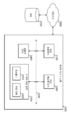
도1은 본 발명의 실시 예에 따른 데이터 저장 장치(10A)를 도시한 블록도이다.1 is a block diagram illustrating a
데이터 저장 장치(10A)는 외부 장치의 라이트 요청에 응답하여, 외부 장치로부터 제공된 데이터를 저장하도록 구성될 수 있다. 또한, 데이터 저장 장치(10A)는 외부 장치의 리드 요청에 응답하여, 저장된 데이터를 외부 장치로 제공하도록 구성될 수 있다.The
데이터 저장 장치(10A)는 PCMCIA(Personal Computer Memory Card International Association) 카드, CF(Compact Flash) 카드, 스마트 미디어 카드, 메모리 스틱, 다양한 멀티 미디어 카드(MMC, eMMC, RS-MMC, MMC-micro), SD(Secure Digital) 카드(SD, Mini-SD, Micro-SD), UFS(Universal Flash Storage) 또는 SSD(Solid State Drive) 등으로 구성될 수 있다.The
데이터 저장 장치(10A)는 컨트롤러(100A) 및 비휘발성 메모리 장치(200A)를 포함할 수 있다.The
컨트롤러(100A)는 데이터 저장 장치(10A)의 제반 동작을 제어할 수 있다. 컨트롤러(100A)는 외부 장치로부터 전송된 라이트 요청에 응답하여 비휘발성 메모리 장치(200A)에 데이터를 저장하고, 외부 장치로부터 전송된 리드 요청에 응답하여 비휘발성 메모리 장치(200A)에 저장된 데이터를 리드하여 외부 장치로 출력할 수 있다.The
컨트롤러(100A)는 적합성 판단부(110A) 및 리드 바이어스 결정부(120A)를 포함할 수 있다.The
적합성 판단부(110A)는 타겟 문턱 전압 분포들에 대해 타겟 리드 바이어스의 적합성을 판단할 수 있다. 타겟 리드 바이어스는, 비휘발성 메모리 장치(200A)가 리드 동작을 위해 사용 중인 리드 바이어스일 수 있다. 즉, 적합성 판단부(110A)는 현재 사용 중인 리드 바이어스의 적합성을 판단할 수 있다. 또한, 실시 예에 따라, 타겟 리드 바이어스는 비휘발성 메모리 장치(200A)가 리드 동작을 위해 앞으로 사용할 리드 바이어스, 예를 들어, 리드 바이어스 결정부(120A)에 의해 결정된 새로운 리드 바이어스일 수 있다. 적합성 판단부(110A)는 잘못 결정된 리드 바이어스가 리드 동작에서 사용되기 전에, 새로운 리드 바이어스의 적합성을 미리 판단할 수 있다.The
한편, 비휘발성 메모리 장치(200A)는 하나의 메모리 셀에 저장된 비트 수에 따라 리드 동작에서 복수의 리드 바이어스들을 사용할 수 있고, 타겟 리드 바이어스는 복수의 리드 바이어스들 중 하나 이상일 수 있다. 다시 말해서, 적합성 판단 동작은 복수의 리드 바이어스들 중 타겟 리드 바이어스로 선택된 리드 바이어스들에 대해 각각 수행될 수 있다. 그리고, 적합성이 판단될 타겟 리드 바이어스가 선택되면, 타겟 문턱 전압 분포들이 타겟 리드 바이어스에 대응하여 결정될 수 있다. 타겟 문턱 전압 분포들은 메모리 셀들의 문턱 전압 분포들 중에서 서로 인접한 문턱 전압 분포들일 수 있다. 타겟 문턱 전압 분포들은 타겟 리드 바이어스로 구분되어야 할 인접한 문턱 전압 분포들일 수 있다. 즉, 본 발명에서 적합성 판단 동작은, 타겟 리드 바이어스가 서로 인접한 타겟 문턱 전압 분포들을 구분할 수 있도록 타겟 문턱 전압 분포들의 사이에 적절히 위치하는지 여부를 판단하기 위한 것일 수 있다.Meanwhile, the
구체적으로, 적합성 판단부(110A)는, 타겟 문턱 전압 분포들의 최적 리드 바이어스에 대한 타겟 리드 바이어스의 오차율을 산출하고 오차율에 근거하여 타겟 리드 바이어스가 최적 리드 바이어스에 대한 허용 오차 범위 내에 존재하는지 여부를 판단함으로써, 적합성 판단 동작을 수행할 수 있다. 최적 리드 바이어스는 타겟 문턱 전압 분포들의 골짜기에 대응하는 전압 레벨일 수 있다. 타겟 리드 바이어스는 최적 리드 바이어스에 대한 허용 오차 범위 내에 존재할 때 적합하다고 판단될 수 있다. 그러나, 타겟 리드 바이어스는 최적 리드 바이어스에 대한 허용 오차 범위 내에 존재하지 않을 때 부적합하다고 판단될 수 있다. 적합성이 인정된 타겟 리드 바이어스는 이후 비휘발성 메모리 장치(200A)의 리드 동작에서 사용될 수 있지만 적합성이 부정된 타겟 리드 바이어스는 리드 동작에서 사용될 수 없고, 따라서, 리드 바이어스 결정부(120A)는 새로운 리드 바이어스를 결정할 수 있다.Specifically, the
리드 바이어스 결정부(120A)는 타겟 문턱 전압 분포들에 대해 새로운 리드 바이어스를 결정하기 위해서, 기울기 최적 알고리즘(Gradient Decent Algorithm, GD_ARG)에 근거하여 리드 바이어스 결정 동작을 수행할 수 있다. 기울기 최적 알고리즘(GD_ARG)에 대한 자세한 설명은 후술될 것이다. 앞서 설명한 바와 같이, 리드 바이어스 결정부(120A)에 의해 결정된 새로운 리드 바이어스는 적합성 판단부(110A)에 의해 타겟 문턱 전압 분포들에 대한 적합성을 판단받을 수 있다.The read
컨트롤러(100A)는 적합성 판단부(110A)에 의해 적합한 것으로 판단된 리드 바이어스들에 근거하여 리드 동작을 수행하도록 비휘발성 메모리 장치(200A)를 제어할 수 있다.The
비휘발성 메모리 장치(200A)는 컨트롤러(100A)의 제어에 따라, 컨트롤러(100A)로부터 전송된 데이터를 저장하고, 저장된 데이터를 리드하여 컨트롤러(100A)로 전송할 수 있다. 비휘발성 메모리 장치(200A)는 컨트롤러(100A)에 의해 결정된 리드 바이어스들에 근거하여 리드 동작을 수행할 수 있다.The
비휘발성 메모리 장치(200A)는 낸드 플래시(NAND Flash) 또는 노어 플래시(NOR Flash)와 같은 플래시 메모리 장치, FeRAM(Ferroelectrics Random Access Memory), PCRAM(Phase-Change Random Access Memory), MRAM(Magnetic Random Access Memory) 또는 ReRAM(Resistive Random Access Memory) 등을 포함할 수 있다.The
한편, 도1은 데이터 저장 장치(10A)가 하나의 비휘발성 메모리 장치(200A)를 포함하는 것으로 도시하나, 본 발명의 실시 예는 이에 제한되지 않는다.On the other hand, Fig. 1 shows that the
도2는 도1의 비휘발성 메모리 장치(200A)의 세부적인 구성을 예시적으로 도시한 블록도이다.2 is a block diagram exemplarily showing a detailed configuration of the
비휘발성 메모리 장치(200A)는 제어 로직(210), 전압 공급부(220), 인터페이스부(230), 어드레스 디코더(240), 데이터 입출력부(250) 및 메모리 영역(260)을 포함할 수 있다.The
제어 로직(210)은 컨트롤러(100A)의 제어에 따라 비휘발성 메모리 장치(200A)의 제반 동작들을 제어할 수 있다. 제어 로직(210)은 컨트롤러(100A)로부터 전송된 커맨드를 인터페이스부(230)로부터 전송받고, 커맨드에 응답하여 제어 신호들을 비휘발성 메모리 장치(200A)의 내부 유닛들로 전송할 수 있다.The
전압 공급부(220)는 제어 로직(210)의 제어에 따라, 비휘발성 메모리 장치(200A)의 제반 동작에 필요한 다양한 동작 전압들을 생성할 수 있다. 예를 들어, 전압 공급부(220)는 리드 동작에서 사용될 리드 바이어스를 어드레스 디코더(240)로 공급할 수 있다.The
인터페이스부(230)는 컨트롤러(100A)와 커맨드 및 어드레스를 포함한 각종 제어 신호들 및 데이터를 주고 받을 수 있다. 인터페이스부(230)는 입력된 각종 제어 신호들 및 데이터를 비휘발성 메모리 장치(200A)의 내부 유닛들로 전송할 수 있다. The
어드레스 디코더(240)는 메모리 영역(260)에서 액세스될 부분을 선택하기 위해 어드레스를 디코딩할 수 있다. 어드레스 디코더(240)는 디코딩 결과에 따라 워드라인들(WL) 중 선택된 워드라인으로 리드 바이어스를 인가할 수 있다. 또한, 어드레스 디코더(240)는 비트라인들(BL)을 선택적으로 구동하도록 데이터 입출력부(250)를 제어할 수 있다.The
데이터 입출력부(250)는 인터페이스부(230)로부터 전송된 데이터를 비트라인들(BL)을 통해 메모리 영역(260)으로 전송할 수 있다. 데이터 입출력부(250)는 메모리 영역(260)으로부터 비트라인들(BL)을 통해 리드된 데이터를 인터페이스부(230)로 전송할 수 있다. 데이터 입출력부(250)는 메모리 영역(260)에 포함된 메모리 셀이 리드 바이어스에 응답하여 온/오프됨에 따라 형성된 커런트를 센싱하고, 센싱 결과에 따라 메모리 셀로부터 리드된 데이터를 획득할 수 있다.The data input /
메모리 영역(260)은 워드라인들(WL)을 통해 어드레스 디코더(240)와 연결될 수 있고, 비트라인들(BL)을 통해 데이터 입출력부(250)와 연결될 수 있다. 메모리 영역(260)은 워드라인들(WL)과 비트라인들(BL)이 교차하는 영역에 각각 배치되고 데이터가 저장되는 복수의 메모리 셀들을 포함할 수 있다. 메모리 영역(260)은 2차원 또는 3차원 구조의 메모리 셀 어레이를 포함할 수 있다.The
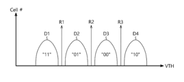
도3a는 메모리 셀들의 문턱 전압 분포들(D1~D4)을 예시적으로 도시하는 도면이다. 가로축(VTH)은 메모리 셀의 문턱 전압을 의미하고, 세로축(Cell #)은 문턱 전압에 대한 메모리 셀들의 개수를 의미할 수 있다. 문턱 전압 분포들(D1~D4)을 형성하는 메모리 셀들은 단일의 워드라인에 연결된 메모리 셀들일 수 있다.FIG. 3A is an exemplary diagram illustrating threshold voltage distributions D1 through D4 of memory cells. The horizontal axis VTH represents the threshold voltage of the memory cell, and the vertical axis Cell # represents the number of memory cells with respect to the threshold voltage. The memory cells forming the threshold voltage distributions D1 through D4 may be memory cells connected to a single word line.
도3a를 참조하면, 메모리 셀들은 저장된 데이터에 따라 일정한 문턱 전압 분포들(D1~D4)을 형성할 수 있다. 메모리 셀은 라이트 동작이 수행될 때, 저장될 2비트의 데이터에 따라 4개의 문턱 전압 분포들(D1~D4) 중 어느 하나에 대응하는 문턱 전압을 가지도록 제어될 수 있다. 예를 들어, 데이터 "11"이 저장된 메모리 셀은 문턱 전압 분포(D1)에 대응하는 문턱 전압을 가질 수 있다. 한편, 도3a는 메모리 셀에 2비트의 데이터가 저장되는 경우를 도시하지만, 본 발명의 실시 예는 이에 제한되지 않는다.Referring to FIG. 3A, the memory cells may form constant threshold voltage distributions D1 to D4 according to stored data. The memory cell can be controlled to have a threshold voltage corresponding to one of the four threshold voltage distributions D1 to D4 according to the two bits of data to be stored when the write operation is performed. For example, a memory cell storing data "11 " may have a threshold voltage corresponding to the threshold voltage distribution D1. On the other hand, FIG. 3A shows a case where two bits of data are stored in a memory cell, but the embodiment of the present invention is not limited thereto.
메모리 셀은 대응하는 워드라인을 통해 소정의 리드 바이어스를 인가받을 때, 자신의 문턱 전압에 따라 턴온되거나 턴오프 상태를 유지할 수 있다. 구체적으로, 메모리 셀은 자신의 문턱 전압보다 높은 리드 바이어스가 인가되면, 턴온될 수 있고, 자신의 문턱 전압보다 낮은 리드 바이어스가 인가되면 턴오프 상태를 유지할 수 있다. 메모리 셀은 턴온/턴오프됨으로써, 대응하는 비트라인에 커런트를 형성할 수 있다. 그리고, 해당 커런트를 센싱함으로써 메모리 셀의 문턱 전압이 인가된 리드 바이어스보다 높은지 또는 낮은지가 판단될 수 있다. 이러한 원리로, 리드 동작이 수행될 때, 리드 바이어스들(R1~R3)이 메모리 셀들의 문턱 전압 분포들(D1~D4)을 구분하기 위해서 메모리 셀들로 인가될 수 있다. 그리고, 메모리 셀이 위치하는 문턱 전압 분포를 판별함으로써 메모리 셀에 저장된 데이터가 획득될 수 있다.The memory cell may be turned on or off according to its threshold voltage when a predetermined read bias is applied through the corresponding word line. Specifically, the memory cell can be turned on when a read bias higher than its own threshold voltage is applied, and can maintain the turn-off state when a read bias lower than its own threshold voltage is applied. The memory cell is turned on / off so that a current can be formed in the corresponding bit line. By sensing the current, it is possible to determine whether the threshold voltage of the memory cell is higher or lower than the applied read bias. With this principle, when the read operation is performed, the read biases R1 to R3 can be applied to the memory cells to distinguish the threshold voltage distributions D1 to D4 of the memory cells. Then, the data stored in the memory cell can be obtained by determining the threshold voltage distribution in which the memory cell is located.
도3b는 문턱 전압 분포들(D1~D4)의 이동을 예시적으로 도시하는 도면이다.FIG. 3B is a diagram exemplarily showing the movement of the threshold voltage distributions D1 to D4.
도3b를 참조하면, 메모리 셀들의 문턱 전압들이 변경됨으로써 문턱 전압 분포들(D1~D4)은 문턱 전압 분포들(D1'~D4')로 이동할 수 있다. 메모리 셀의 문턱 전압의 변화는 인접하는 메모리 셀들 간의 간섭이나 시간의 경과에 따른 방전 등에 기인하여 발생할 수 있다.Referring to FIG. 3B, the threshold voltage distributions D1 to D4 can be shifted to the threshold voltage distributions D1 'to D4' by changing the threshold voltages of the memory cells. The change in the threshold voltage of the memory cell may occur due to interference between adjacent memory cells or discharge over time.
이때, 리드 바이어스들(R1~R3)은 문턱 전압 분포들(D1'~D4')을 구별하기에 부적절할 수 있다. 메모리 셀들이 문턱 전압 분포들(D1'~D4')을 형성할 때, 리드 바이어스들(R1~R3)에 근거하여 메모리 셀들로부터 리드된 데이터는 컨트롤러(100A)의 에러 정정 능력을 초과하는 에러 비트들을 포함할 수 있다. 즉, 리드 바이어스들(R1~R3)을 사용한 리드 동작은 실패할 수 있다.At this time, the read biases R1 to R3 may be inadequate for distinguishing the threshold voltage distributions D1 'to D4'. When the memory cells form threshold voltage distributions D1 'to D4', the data read from the memory cells based on the read biases R1 to R3 is the error bit that exceeds the error correction capability of the
도3c는 문턱 전압 분포들(D1'~D4')에 대한 최적 리드 바이어스들(R1OP~R3OP)을 도시하는 도면이다.3C is a diagram showing optimal read biases R1OP to R3OP for the threshold voltage distributions D1 'to D4'.
도3c를 참조하면, 최적 리드 바이어스들(R1OP~R3OP)은 이동된 문턱 전압 분포들(D1'~D4')의 골짜기에 위치할 수 있다. 최적 리드 바이어스들(R1OP~R3OP)은, 문턱 전압 분포들(D1'~D4')을 형성하는 메모리 셀들로부터 리드된 데이터가 최소한의 에러 비트들을 포함하도록 하는 리드 바이어스들일 수 있다. 메모리 셀들이 문턱 전압 분포들(D1'~D4')을 형성할 때, 최적 리드 바이어스들(R1OP~R3OP)에 근거하여 메모리 셀들로부터 리드된 데이터는 컨트롤러(100A)의 에러 정정 능력 내의 에러 비트들을 포함할 수 있다. 즉, 최적 리드 바이어스들(R1OP~R3OP)을 사용한 리드 동작은 성공할 수 있다.Referring to FIG. 3C, the optimal read biases R1OP to R3OP may be located in the valleys of shifted threshold voltage distributions D1 'to D4'. The optimum read biases R1OP to R3OP may be lead biases that cause the data read from the memory cells forming the threshold voltage distributions D1 'to D4' to include the least error bits. When the memory cells form threshold voltage distributions D1 'to D4', the data read from the memory cells based on the optimal read biases R1OP to R3OP are the error bits in the error correction capability of the
다시 도1을 참조하면, 리드 바이어스 결정부(120A)는, 문턱 전압 분포들(D1~D4)이 문턱 전압 분포들(D1'~D4')로 이동할 경우, 최적 리드 바이어스들(R1OP~R3OP)을 새로운 리드 바이어스들로 결정하기 위해서 리드 바이어스 결정 동작을 수행할 수 있다.1, when the threshold voltage distributions D1 to D4 are shifted to the threshold voltage distributions D1 'to D4', the read
도3d는 문턱 전압 분포들(D1'~D4')에 대해 오작동한 리드 바이어스 결정 동작을 예시적으로 도시하는 도면이다.FIG. 3D is an exemplary diagram illustrating a read bias determination operation that malfunctions with respect to the threshold voltage distributions D1 'to D4'.
도3d를 참조하면, 리드 바이어스 결정 동작의 오작동에 의해, 문턱 전압 분포들(D1'~D4')에 대해 새로운 리드 바이어스들(R1F~R3F)이 결정될 수 있다. 이러한 리드 바이어스 결정 동작의 오작동은 후술될 바와 같이 기울기 최적 알고리즘(GD_ARG)이 오작동함으로써 발생할 수 있다. 새로운 리드 바이어스들(R1F~R3F)은 모든 문턱 전압 분포들(D1'~D4')을 구별하지 못하므로 리드 동작을 수행하는 데 부적합할 것이다. 따라서, 새로운 리드 바이어스들(R1F~R3F)에 근거한 리드 동작은 실패할 수 있다.Referring to FIG. 3D, new read biases R1F to R3F can be determined for the threshold voltage distributions D1 'to D4' by a malfunction of the read bias determination operation. The malfunction of the read bias determination operation may occur due to a malfunction of the gradient optimization algorithm GD_ARG as described later. The new read biases R1F to R3F will not be able to distinguish all of the threshold voltage distributions D1 'to D4' and thus will be unsuitable for performing the read operation. Therefore, the read operation based on the new read biases R1F to R3F may fail.
본 발명의 실시 예에 따르면, 적합성 판단부(110A)는 현재 사용 중인 리드 바이어스 또는 리드 바이어스 결정부(120A)에 의해 결정된 리드 바이어스의 적합성을 간이한 방법을 통해 효율적으로 판단할 수 있다.According to the embodiment of the present invention, the
도4a 내지 도4c는 도1의 적합성 판단부(110A)가 타겟 리드 바이어스 및 타겟 문턱 전압 분포들을 결정하는 방법을 예시적으로 설명하기 위한 도면들이다. 도4a 내지 도4c는, 오작동한 리드 바이어스 결정 동작에 의해 문턱 전압 분포들(D1'~D4')에 대해 리드 바이어스들(R1F~R3F)이 잘못 결정된 상황에서, 타겟 리드 바이어스 및 타겟 문턱 전압 분포들을 결정하는 방법을 도시한다.FIGS. 4A to 4C are diagrams for illustrating an exemplary method of determining the target read bias and target threshold voltage distributions by the
도4a를 참조하면, 적합성 판단부(110A)는 리드 바이어스(R1F)를 타겟 리드 바이어스로 선택할 수 있다. 리드 동작에서 타겟 리드 바이어스(R1F)는 문턱 전압 분포들(D1', D2')을 구분하기 위해 사용될 것이므로, 문턱 전압 분포들(D1', D2')이 타겟 문턱 전압 분포들로 결정될 수 있다.Referring to FIG. 4A, the
도4b를 참조하면, 적합성 판단부(110A)는 리드 바이어스(R2F)를 타겟 리드 바이어스로 선택할 수 있다. 리드 동작에서 타겟 리드 바이어스(R2F)는 문턱 전압 분포들(D2', D3')을 구분하기 위해 사용될 것이므로, 문턱 전압 분포들(D2', D3')이 타겟 문턱 전압 분포들로 결정될 수 있다. Referring to FIG. 4B, the
도4c를 참조하면, 적합성 판단부(110A)는 리드 바이어스(R3F)를 타겟 리드 바이어스로 선택할 수 있다. 리드 동작에서 타겟 리드 바이어스(R3F)는 문턱 전압 분포들(D3', D4')을 구분하기 위해 사용될 것이므로, 문턱 전압 분포들(D3', D4')이 타겟 문턱 전압 분포들로 결정될 수 있다. Referring to FIG. 4C, the
정리하면, 적합성 판단부(110A)는 리드 바이어스들(R1F~R3F) 및 문턱 전압 분포들(D1'~D4')의 순서에 근거하여, 타겟 리드 바이어스에 대응하는 타겟 문턱 전압 분포들을 결정할 수 있다.In short, the
도5는 도1의 적합성 판단부(110A)의 동작 방법을 예시적으로 도시하는 도면이다. 도5에서 적합성 판단부(110A)는, 예를 들어, 도4b의 타겟 리드 바이어스(R2F)가 타겟 문턱 전압 분포들(D2', D3')에 대해 적합한지 여부를 판단할 것이다.5 is a diagram exemplarily showing a method of operation of the
도5를 참조하면, 우선, 적합성 판단부(110A)는 타겟 리드 바이어스(R2F)보다 작은 문턱 전압을 가진 것으로 판단되는 타겟 메모리 셀들의 개수, 즉, 판단 셀 개수를 판단할 수 있다. 적합성 판단부(110A)는, 타겟 리드 바이어스(R2F)가 타겟 메모리 셀들로 인가될 때 턴온되는 타겟 메모리 셀들의 개수를 판단 셀 개수로서 판단할 수 있다. 적합성 판단부(110A)는, 타겟 리드 바이어스(R2F)가 타겟 메모리 셀들로 인가될 때 타겟 메모리 셀들로부터 리드되는 데이터를 획득하고 획득된 데이터에서 소정 값, 예를 들어, "1"들을 카운트함으로써, 판단 셀 개수를 판단할 수 있다. 도5를 참조하면, 예를 들어, 전체 "400"개의 타겟 메모리 셀들에 대해 판단 셀 개수는 "290"일 수 있다.Referring to FIG. 5, first, the
그리고, 적합성 판단부(110A)는 판단 셀 개수와 비교할 기준 셀 개수를 결정할 수 있다. 기준 셀 개수는, 문턱 전압 분포들(D1'~D4')에 대응하는 메모리 셀들의 개수가 균등할 때, 최적 리드 바이어스(R2OP)보다 작은 문턱 전압을 가진 것으로 추정되는 타겟 메모리 셀들의 개수일 수 있다. 다시 말하면, 기준 셀 개수는, 문턱 전압 분포들(D1'~D4')에 대응하는 메모리 셀들의 개수가 균등할 때, 최적 리드 바이어스(R2OP)가 타겟 메모리 셀들로 인가된다면 턴온될 것으로 추정되는 타겟 메모리 셀들의 개수일 수 있다. 따라서, 기준 셀 개수는 타겟 리드 바이어스 또는 타겟 문턱 전압 분포들이 무엇인지에 따라 결정될 수 있다. 도5를 참조하면, 타겟 문턱 전압 분포들(D2', D3')에 대한 기준 셀 개수는 "200"일 수 있다.The
그리고, 적합성 판단부(110A)는 판단 셀 개수와 기준 셀 개수에 근거하여 타겟 리드 바이어스(R2F)의 적합성을 판단할 수 있다. 예를 들어, 적합성 판단부(110A)는 아래의 식(1)에 근거한 판단 셀 개수와 기준 셀 개수의 오차율(Pr_DF)이 소정의 허용 오차 범위에 포함될 때 타겟 리드 바이어스(R2F)가 적합하다고 판단할 수 있다. 오차율(Pr_DF)이 작을수록, 타겟 리드 바이어스(R2F)는 최적 리드 바이어스(R2OP)에 근접할 수 있다.The
식(1) Pr _DF=(판단 셀 개수-기준 셀 개수)/문턱 전압 분포 당 타겟 메모리 셀들의 개수. Pr _DF = (number of cells to be judged - number of cells to be counted) / number of target memory cells per threshold voltage distribution .
도5에서 적합성 판단부(110A)는 타겟 리드 바이어스(R2F)의 오차율(Pr_DF)을 "0.9"로 판단할 수 있다. 이때, 적합성 판단부(110A)는 타겟 리드 바이어스(R2F)가 최적 리드 바이어스(R2OP)에 대한 소정의 허용 오차 범위에 포함되지 않는다고 판단하고, 타겟 리드 바이어스(R2F)는 타겟 문턱 전압 분포들(D2', D3')에 대해 부적합한 것으로 판단할 수 있다. 따라서, 리드 바이어스 결정부(120A)는 잘못 결정된 타겟 리드 바이어스(R2F) 대신 새로운 리드 바이어스를 결정하기 위해서 리드 바이어스 결정 동작을 다시 수행할 수 있다. In Fig. 5, the
한편, 적합성 판단부(110A)는 기준 셀 개수를 결정하여야 하고, 기준 셀 개수는 문턱 전압 분포들(D1'~D4')에 각각 대응하는 타겟 메모리 셀들의 개수에 근거하여 결정될 수 있다. 따라서, 만일, 데이터가 랜더마이징된 후에 비휘발성 메모리 장치에 저장되는 경우라면, 문턱 전압 분포들(D1'~D4')이 동일한 개수의 타겟 메모리 셀들에 각각 대응되는 것으로 가정하고 상술한 바와 같이 기준 셀 개수를 결정할 수 있을 것이다.On the other hand, the
도6a는 기울기 최적 알고리즘(GD_ARG)에 근거한 리드 바이어스 결정 동작을 예시적으로 도시하는 도면이다. 도6a는 임의의 타겟 문턱 전압 분포들(TD1, TD2)에 대해 기울기 최적 알고리즘(GD_ARG)에 근거한 리드 바이어스 결정 동작이 어떻게 수행되는지를 보여준다.6A is a diagram exemplarily showing a read bias determination operation based on a gradient optimization algorithm (GD_ARG). 6A shows how the read bias decision operation based on the gradient optimization algorithm GD_ARG is performed for any target threshold voltage distributions TDl, TD2.
도6a를 참조하면, 기울기 최적 알고리즘(GD_ARG)에 근거한 리드 바이어스 결정 동작은 인접한 임의의 타겟 문턱 전압 분포들(TD1, TD2)에서 기울기가 "0"인 위치에 대응하는 전압 레벨을 찾도록 진행될 수 있다. Referring to FIG. 6A, the read bias determination operation based on the gradient optimization algorithm GD_ARG can be proceeded to find a voltage level corresponding to a position with a slope "0" in any adjacent target threshold voltage distributions TDl, TD2 have.
구체적으로, 리드 바이어스 결정 동작이 수행될 때, 소정의 시작 바이어스(ST)인 테스트 바이어스(T2)를 포함하는 적어도 3개의 테스트 바이어스들(T1~T3)에 근거하여 데이터가 리드될 수 있다. 그리고, 리드된 데이터를 통해 테스트 바이어스들(T1~T3) 사이의 구간들에 대응하는 메모리 셀들의 개수가 산출될 수 있다. 그리고, 산출 결과에 근거하여 테스트 바이어스들(T1~T3) 사이의 구간들에 대응하는 타겟 문턱 전압 분포(TD2)의 기울기가 추정될 수 있다. Specifically, when the read bias determination operation is performed, data may be read based on at least three test biases T1 to T3 including a test bias T2 which is a predetermined start bias ST. Then, the number of memory cells corresponding to the intervals between the test biases T1 to T3 can be calculated through the read data. Then, based on the calculation result, the slope of the target threshold voltage distribution TD2 corresponding to the intervals between the test biases T1 to T3 can be estimated.
이어서, 시작 바이어스(ST)에 대해 기울기의 크기가 감소하는 방향(A)에서 테스트 바이어스들(T4, T5)이 추가적으로 선택되고, 테스트 바이어스들(T3~T5) 사이의 구간들에 대응하는 타겟 문턱 전압 분포(TD2)의 기울기가 동일한 방식으로 추정될 수 있다. 이때, 테스트 바이어스들의 선택 및 기울기의 추정은 타겟 문턱 전압 분포(TD2)에서 기울기가 "0"인 위치가 발견될 때까지 선택 방향을 변경하면서 계속될 수 있다. 그리고, 기울기가 "0"인 위치가 발견될 때, 마지막으로 선택된 3개의 테스트 바이어스들 중에서 중간 테스트 바이어스가 새로운 리드 바이어스로 선택될 수 있다. 예를 들어, 도6a에서는 테스트 바이어스(T4)가 새로운 리드 바이어스로 선택될 수 있다.The test biases T4 and T5 are additionally selected in the direction A in which the magnitude of the gradient decreases with respect to the start bias ST and the target thresholds corresponding to the intervals between the test biases T3 and T5 The slope of the voltage distribution TD2 can be estimated in the same manner. At this time, the selection of the test biases and the estimation of the slope can be continued while changing the selection direction until a position with a slope "0" is found in the target threshold voltage distribution TD2. Then, when a position with a slope of "0" is found, among the last three selected test biases, the intermediate test bias can be selected as the new lead bias. For example, in FIG. 6A, the test bias T4 may be selected as a new lead bias.
이러한 기울기 최적 알고리즘(GD_ARG)에서는 시작 바이어스(ST)의 위치가 결과에 중요한 영향을 미칠 수 있다. 도6b에 도시된 바와 같이, 시작 바이어스(ST)의 위치에 따라 기울기 최적 알고리즘(GD_ARG)은 오작동할 수 있다.In this slope optimization algorithm (GD_ARG), the position of the start bias (ST) can have a significant effect on the result. As shown in Fig. 6B, the slope optimization algorithm GD_ARG may malfunction depending on the position of the start bias ST.
도6b는 오작동한 기울기 최적 알고리즘(GD_ARG)에 근거한 리드 바이어스 결정 동작을 예시적으로 도시하는 도면이다.6B is a diagram exemplarily showing a read bias determination operation based on a malfunctioning gradient optimization algorithm (GD_ARG).
도6b를 참조하면, 우선, 도6a의 타겟 문턱 전압 분포들(TD1, TD2)은 타겟 문턱 전압 분포들(TD1', TD2')로 이동하였지만, 시작 바이어스(ST)는 도6a와 동일하게 테스트 바이어스(T2)인 것으로 가정할 것이다. 이러한 상황은, 기설정된 시작 바이어스(ST)의 위치가 타겟 문턱 전압 분포들(TD1, TD2)의 큰 이동에 의해 부적절하게 된 경우일 것이다.Referring to FIG. 6B, the target threshold voltage distributions TD1 and TD2 of FIG. 6A are shifted to the target threshold voltage distributions TD1 'and TD2' Bias < / RTI > (T2). This situation may be the case where the position of the predetermined start bias ST becomes inadequate due to a large shift of the target threshold voltage distributions TD1 and TD2.
리드 바이어스 결정 동작이 수행될 때, 도6a를 참조하여 설명된 방식대로, 소정의 시작 바이어스(ST)인 테스트 바이어스(T2)를 포함하는 적어도 3개의 테스트 바이어스들(T1', T2, T3')에 근거하여 타겟 문턱 전압 분포(TD2')의 기울기가 추정되기 시작할 것이다. 그리고, 테스트 바이어스들의 선택 및 기울기의 추정은 시작 바이어스(ST)에 대해 기울기의 크기가 감소하는 방향(B)으로 진행될 수 있다. 따라서, 테스트 바이어스들(T4', T5')이 선택되고, 결국, 테스트 바이어스(T4')가 타겟 문턱 전압 분포들(TD1', TD2')의 새로운 리드 바이어스로 잘못 결정될 수 있다.When the read bias determination operation is performed, at least three test biases T1 ', T2, T3' including a test bias T2 which is a predetermined start bias ST are generated in the manner described with reference to FIG. 6A, The slope of the target threshold voltage distribution TD2 'will start to be estimated. Then, the selection of the test biases and the estimation of the slope may proceed in the direction B in which the magnitude of the gradient decreases with respect to the start bias ST. Thus, the test biases T4 ', T5' are selected and eventually the test bias T4 'may be erroneously determined as the new lead bias of the target threshold voltage distributions TD1', TD2 '.
이처럼, 최적 리드 바이어스(ROP)가 위치한 방향(A)과 반대 방향(B)으로 진행된 기울기 최적 알고리즘(GD_ARG)의 오작동은, 시작 바이어스(ST)가 최적 리드 바이어스(ROP)에서 너무 멀어지게 될 때 발생할 수 있다. 물론, 시작 바이어스(ST)의 위치는 애초부터 잘못 설정될 수도 있지만, 타겟 문턱 전압 분포들(TD1, TD2)의 예상 이동량을 고려하여 적절하게 기설정되더라도 타겟 문턱 전압 분포들(TD1, TD2)이 너무 크게 이동함으로써 부적절하게 될 수도 있다.The malfunction of the slope optimization algorithm GD_ARG proceeding in the opposite direction B with respect to the direction A in which the optimum read bias ROP is located is obtained when the start bias ST becomes too far from the optimum lead bias ROP Lt; / RTI > Of course, the position of the start bias ST may be erroneously set from the beginning, but the target threshold voltage distributions TD1 and TD2 may be set to be equal to or smaller than the target threshold voltage distributions TD1 and TD2 even if appropriately set in consideration of the expected amount of movement of the target threshold voltage distributions TD1 and TD2 It can be made improper by moving too large.
그러나, 본 발명의 적합성 판단부(110A)는, 리드 바이어스 결정 동작이 오작동하더라도 리드 바이어스의 적합성을 간이한 방법으로 판단하여 리드 바이어스 결정 동작이 재수행되도록 할 수 있다.However, even if the read bias determination operation is malfunctioning, the
한편, 컨트롤러(100A)는 적합성 판단 동작에서 산출된 오차율(Pr_DF)에 근거하여, 시작 바이어스(ST)가 최적 리드 바이어스(R2OP)에 대해 위치한 방향을 추정할 수 있을 것이다. 예를 들어, 오차율(Pr_DF)이 양수일 때, 시작 바이어스(ST)는 도6b에 도시된 바와 같이 최적 리드 바이어스(R2OP)에서 우측으로 멀리 위치한 것으로 추정할 수 있다. 따라서, 컨트롤러(100A)는 시작 바이어스(ST)를 적절한 방향(A)으로 이동시킬 수 있다. 결국, 리드 바이어스 결정부(120A)는 새로운 시작 바이어스에 근거하여 리드 바이어스 결정 동작을 다시 수행할 수 있다.On the other hand, the
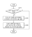
도7은 도1의 데이터 저장 장치(10A)의 동작 방법을 예시적으로 도시하는 순서도이다.FIG. 7 is a flowchart exemplarily showing a method of operating the
단계(S110)에서, 적합성 판단부(110A)는 타겟 문턱 전압 분포들에 대한 타겟 리드 바이어스의 적합성을 판단할 수 있다. 적합성 판단부(110A)는 타겟 문턱 전압 분포들의 최적 리드 바이어스에 대한 타겟 리드 바이어스의 오차율을 산출하고 오차율에 근거하여 타겟 리드 바이어스가 최적 리드 바이어스에 대한 허용 오차 범위 내에 존재하는지 여부를 판단함으로써, 타겟 리드 바이어스의 적합성을 판단할 수 있다. 그리고, 타겟 리드 바이어스가 적합한 것으로 판단될 때, 절차는 종료할 수 있다. 그러나, 타겟 리드 바이어스가 부적합한 것으로 판단될 때, 절차는 단계(S120)로 이동할 수 있다.In step S110, the
단계(S120)에서, 리드 바이어스 결정부(120A)는 기울기 최적 알고리즘(GD_ARG)에 근거하여 타겟 문턱 전압 분포들에 대해 새로운 리드 바이어스를 결정할 수 있다. 리드 바이어스 결정부(120A)는 소정의 시작 바이어스로부터 타겟 문턱 전압 분포들에서 기울기가 "0"인 위치에 대응하는 전압 레벨을 찾도록 진행됨으로써 새로운 리드 바이어스를 결정할 수 있다.In step S120, the read
도8은 본 발명의 실시 예에 따른 데이터 저장 장치(10B)를 도시한 블록도이다.8 is a block diagram illustrating a
데이터 저장 장치(10B)는 컨트롤러(100B) 및 비휘발성 메모리 장치(200B)를 포함할 수 있다. 컨트롤러(100B)는 적합성 판단부(110B), 리드 바이어스 결정부(120B) 및 시작 바이어스 결정부(130B)를 포함할 수 있다. 적합성 판단부(110B) 및 리드 바이어스 결정부(120B)는 도1의 적합성 판단부(110A) 및 리드 바이어스 결정부(120A)와 실질적으로 동일하게 구성되고 동작할 수 있고, 따라서, 상세한 설명은 생략될 것이다.The
시작 바이어스 결정부(130B)는, 적합성 판단부(110B)가 타겟 문턱 전압 분포들에 대해 타겟 리드 바이어스를 부적합한 것으로 판단할 때, 타겟 문턱 전압 분포들에 대해 수행될 리드 바이어스 결정 동작의 시작 바이어스를 결정할 수 있다. 시작 바이어스 결정부(130B)는 가우시안 모델링 알고리즘(GM_ARG)에 근거하여 시작 바이어스를 결정할 수 있다. 특히, 시작 바이어스 결정부(130B)는 타겟 문턱 전압 분포들의 최적 리드 바이어스에 근접하도록 시작 바이어스를 결정할 수 있다. 즉, 도6d를 참조하여 설명한 바와 같이, 기울기 최적 알고리즘(GD_ARG)은 시작 바이어스가 타겟 문턱 전압 분포들의 최적 리드 바이어스에서 크게 멀어질 때 오작동할 수 있으므로, 시작 바이어스 결정부(130B)는 최적 리드 바이어스에 근접하도록 시작 바이어스를 결정할 수 있다.The start
구체적으로, 시작 바이어스 결정부(130B)는 가우시안 분포 함수에 근거하여 타겟 문턱 전압 분포들 중 선택된 제1 타겟 문턱 전압 분포의 평균 문턱 전압을 결정하고, 평균 문턱 전압 및 제1 타겟 문턱 전압 분포의 추정 폭에 근거하여 시작 바이어스를 결정할 수 있다.Specifically, the start
정리하면, 시작 바이어스 결정부(130B)는, 리드 바이어스 결정 동작에서 사용될, 보다 적절한 시작 바이어스를 결정할 수 있다. 리드 바이어스 결정부(120B)는 결정된 시작 바이어스를 사용하여 기울기 최적 알고리즘(GD_ARG)에 근거한 리드 바이어스 결정 동작을 수행할 수 있다.In summary, the start
한편, 시작 바이어스 결정부(130B)는 시간이 경과하는 동안 동일한 타겟 문턱 전압 분포들에 대해 가우시안 모델링 알고리즘(GM_ARG)에 근거한 시작 바이어스 결정 동작을 복수회 수행할 수 있다. 이때, 시작 바이어스 결정부(130B)는 동일한 타겟 문턱 전압 분포들에 대해 복수의 시작 바이어스들을 산출할 것이다. 따라서, 실시 예에 따라, 시작 바이어스 결정부(130B)는 시간이 경과하는 동안 동일한 타겟 문턱 전압 분포들에 대해 산출된 시작 바이어스들의 평균을 새로운 시작 바이어스로 결정할 수 있다.On the other hand, the start
도9a는 도8의 시작 바이어스 결정부(130B)가 타겟 문턱 전압 분포들(TD1, TD2)에 대한 리드 바이어스 결정 동작을 위한 시작 바이어스(SV2)를 결정하는 방법을 예시적으로 도시하는 도면이다.9A is an exemplary diagram illustrating a method of determining the start bias SV2 for the read bias determination operation for the target threshold voltage distributions TD1 and TD2 in the start
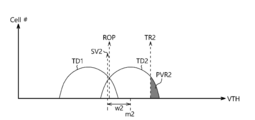
시작 바이어스 결정부(130B)는 타겟 문턱 전압 분포들(TD1, TD2) 중 선택된 어느 하나(TD2)의 평균 문턱 전압(m2)을 산출할 수 있다. 평균 문턱 전압(m2)이 산출되는 타겟 문턱 전압 분포(TD2)는 타겟 문턱 전압 분포들(TD1, TD2) 중에서 기준 리드 바이어스(TR2)가 위치하는 타겟 문턱 전압 분포일 수 있다. 시작 바이어스 결정부(130B)는 선택된 타겟 문턱 전압 분포(TD2) 상에서 기준 리드 바이어스(TR2)에 의해 형성된 부분 분포(PVR2)의 면적률에 근거하여 타겟 문턱 전압 분포(TD2)의 평균 문턱 전압(m2)을 결정할 수 있다. 부분 분포(PVR2)의 면적률은 타겟 문턱 전압 분포(TD2)에 대한 부분 분포(PVR2)의 비율일 수 있다. 다른 말로 하면, 부분 분포(PVR2)의 면적률은 타겟 메모리 셀이 타겟 문턱 전압 분포(TD2) 중 부분 분포(PVR2)에 존재할 확률일 수 있다.The start
한편, 면적률 산출의 오버헤드를 줄이기 위해서 시작 바이어스 결정부(130B)는, 적합성 판단부(110B)가 적합성을 판단한 타겟 리드 바이어스를 기준 리드 바이어스(TR2)로 간주하고 타겟 리드 바이어스의 오차율(Pr_DF)로부터 면적률을 용이하게 산출할 수 있다. 예를 들어, 오차율(Pr_DF)이 양수로 산출된 타겟 리드 바이어스는 최적 리드 바이어스(ROP)의 우측, 즉, 타겟 문턱 전압 분포(TD2)에 위치하므로 기준 리드 바이어스(TR2)로 둘 수 있다. 이때, 부분 분포(PVR2)의 면적률(Pr_PVR2)과 오차율(Pr_DF)의 관계는 아래의 식(2)와 같을 수 있다.On the other hand, in order to reduce the overhead of the area ratio calculation, the start
식(2) ![]()
![]()
계속해서, 시작 바이어스 결정부(130B)는 부분 분포(PVR2)의 면적률(Pr_PVR2)에 근거하여 타겟 문턱 전압 분포(TD2)의 평균 문턱 전압(m2)을 결정할 수 있다. 구체적으로, 타겟 문턱 전압 분포(TD2)는 가우시안 모델링됨으로써 아래의 식(3)으로 표현될 수 있다. 아래 식(3)에서, "vth"는 문턱 전압 축(VTH)의 값이고, "σ"는 타겟 문턱 전압 분포(TD2)의 분산일 수 있다.Subsequently, the start
식(3) ![]()
![]()
따라서, 부분 분포(PVR2)의 면적률(Pr_PVR2) 또는 타겟 리드 바이어스(TR2)의 오차율(Pr_DF)에 대해 아래의 적분 방정식(4)가 성립될 수 있다.Therefore, the following integral equation (4) can be established for the area ratio Pr_PVR2 of the partial distribution PVR2 or the error rate Pr_DF of the target lead bias TR2.
식(4) ![]()
![]()
따라서, 타겟 문턱 전압 분포(TD2)의 분산(σ)이 적절한 상수로 설정되면 식(4)로부터 평균 문턱 전압(m2)이 결정될 수 있다.Therefore, if the variance? Of the target threshold voltage distribution TD2 is set to an appropriate constant, the average threshold voltage m2 can be determined from equation (4).
실시 예에 따라, 상기 식(4)의 연산을 수행하지 않고, Q 함수 특성을 이용하여 부분 분포(PVR2)의 면적률(Pr_PVR2)로부터 평균 문턱 전압(m2)이 간이하게 결정될 수 있다.According to the embodiment, the average threshold voltage m2 from the area ratio Pr_PVR2 of the partial distribution PVR2 can be simply determined by using the Q function property without performing the calculation of the above equation (4).
구체적으로, 가우시안 분포인 타겟 문턱 전압 분포(TD2)는 표준 가우시안 분포로서 표준화될 수 있고, 표준화된 타겟 문턱 전압 분포(STD2)는 아래 식(5)로 변환될 수 있다.Specifically, the target threshold voltage distribution (TD2), which is a Gaussian distribution, can be normalized as a standard Gaussian distribution, and the normalized target threshold voltage distribution (STD2) can be transformed into the following equation (5).
식(5) ![]()
![]()
그리고, 아래 식(6)으로 표현되는 Q 함수는 표준 가우시안 분포의 확률 변수가 "z"보다 큰 값일 확률을 의미할 수 있다.And the Q function expressed by the following equation (6) can mean the probability that the probability variable of the standard Gaussian distribution is a value larger than "z".
식(6) ![]()
![]()
따라서, 아래 식(7)이면, 식(4)와 식(6)에 근거하여 식(8)이 성립할 수 있다.Therefore, Equation (8) can be established based on Equation (4) and Equation (6) if Equation (7) is given below.
식(7) ![]()
![]()
식(8) ![]()
![]()
한편, z 값에 대한 Q(z) 값은 알려져 있으므로, Q(z) 값을 알면 역으로 z 값을 알 수 있다. 따라서, 최종적으로 식(7)과 식(8)을 통해 아래 식(9)가 도출될 수 있다. 아래에서, Q-1은 Q(z)의 역함수일 수 있다.On the other hand, since the value of Q (z) with respect to the z value is known, knowing the value of Q (z) can reverse the value of z. Therefore, finally, the following equation (9) can be derived from the equations (7) and (8). Below, Q-1 can be the inverse of Q (z).
식(9) ![]()
![]()
또한, 식(2) 및 식(9)를 통해 타겟 리드 바이어스(TR2)의 오차율(Pr_DF)에 관한 아래 식(10)이 도출될 수 있다.Further, the following equation (10) can be derived regarding the error rate Pr_DF of the target lead bias TR2 through the expressions (2) and (9).
식(10) ![]()
![]()
![]()
![]()
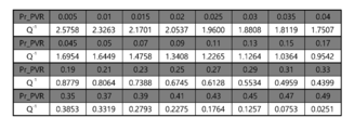
도10은 소정의 면적률들(Pr_PVR)에 대한 Q 함수의 역함수 값들(Q-1)이 예시적으로 정리된 테이블이다.FIG. 10 is a table in which the inverse values (Q -1 ) of the Q function for predetermined area ratios Pr_PVR are exemplified.
시작 바이어스 결정부(130B)는 도10의 테이블을 참조하여, 부분 분포(PVR2)의 면적률(Pr_PVR2)에 대응하는 Q 함수의 역함수 값(Q-1)을 추출할 수 있다. 그리고, 시작 바이어스 결정부(130B)는 기준 리드 바이어스(TR2), Q 함수의 역함수 값(Q-1) 및 소정의 분산(σ)에 근거하여 상기 식(9)를 계산함으로써 평균 문턱 전압(m2)을 효율적으로 산출할 수 있다.The start
한편, 표준 가우시안 분포의 꼬리 근처에서는 면적률(Pr_PVR)에 대한 Q 함수의 역함수 값(Q-1)의 변화가 크기 때문에 테이블은 오차를 줄이기 위하여, 0부터 소정 값, 예를 들어, "0.05"까지 보다 세밀하게 설정된 면적률들(Pr_PVR) 및 대응하는 Q 함수의 역함수 값들(Q-1)을 포함할 수 있다.On the other hand, in the vicinity of the tail of the standard Gaussian distribution, since the inverse value (Q -1 ) of the Q function with respect to the area ratio (Pr_PVR) is large, the table has a predetermined value, for example, "0.05" (Pr_PVR) and the inverse function values (Q- 1 ) of the corresponding Q function up to a predetermined threshold value.
한편, 테이블이 0.5 미만의 면적률(Pr_PVR)에 대해서만 구성되더라도 컨트롤러(100A)는 Q 함수의 대칭성에 근거하여 0.5 초과의 면적률(Pr_PVR)에 대한 Q 함수의 역함수 값(Q-1)도 용이하게 산출할 수 있다. 실시 예에 따라, 테이블은 0.5 초과의 면적률(Pr_PVR)에 대응하는 값도 포함하도록 구성될 수 있다.On the other hand, even if the table is constructed only for the area ratio Pr_PVR of less than 0.5, the
다시 도9a를 참조하면, 시작 바이어스 결정부(130B)는 평균 문턱 전압(m2) 및 타겟 문턱 전압 분포(TD2)의 추정 폭(w2)에 근거하여 시작 바이어스(SV2)를 설정할 수 있다. 시작 바이어스(SV2)는 평균 문턱 전압(m2)이 타겟 문턱 전압 분포(TD2)의 좌측 꼬리 근처로 추정 폭(w2)만큼 이동됨으로써 설정될 수 있다. 시작 바이어스(SV2)는 타겟 문턱 전압 분포(TD2)의 좌측 꼬리 근처로 이동됨으로써 최적 리드 바이어스(ROP)에 근접하게 위치할 수 있다. 시작 바이어스(SV2)는 최종적으로 아래 식(11)로 표현될 수 있다.9A, the start
식(11) ![]()
![]()
즉, 상기 식(11)에서 마지막 항은 평균 문턱 전압(m2)을 타겟 문턱 전압 분포(TD2)의 좌측 꼬리 근처로 이동시키기 위한 것이고, 추정 폭(w)에 대응할 수 있다. 실시 예에 따라, 식(11)의 마지막 항에서 Q-1 함수의 입력값은 "0.999" 대신에 타겟 문턱 전압 분포(TD2)의 형상에 따라 적절한 값이 선택될 수 있을 것이다.That is, the last term in the equation (11) is for moving the average threshold voltage m2 to the left tail of the target threshold voltage distribution TD2 and may correspond to the estimated width w. According to the embodiment, the input value of the Q -1 function in the last term of Equation (11) may be selected to be an appropriate value according to the shape of the target threshold voltage distribution (TD2) instead of "0.999 ".
그리고, 상기 식(11)은 식(2)에 근거하여 타겟 리드 바이어스(TR2)의 오차율(Pr_DF)을 사용한 아래 식(12)으로 표현될 수 있다.The above equation (11) can be expressed by the following equation (12) using the error rate Pr_DF of the target read bias TR2 based on the equation (2).
식(12) ![]()
![]()
정리하면, 시작 바이어스(SV2)는 타겟 문턱 전압 분포들(TD1, TD2)의 최적 리드 바이어스(ROP)에 근접하도록 설정될 수 있다. 따라서, 시작 바이어스(SV2)에 근거한 기울기 최적 알고리즘(GD_ARG)은 잘못된 방향으로 진행하지 않고 최적 리드 바이어스(ROP)의 근처에서 새로운 리드 바이어스를 적절하게 결정할 수 있다.In summary, the start bias SV2 can be set to approach the optimum lead bias (ROP) of the target threshold voltage distributions TD1 and TD2. Therefore, the gradient optimization algorithm GD_ARG based on the start bias SV2 can appropriately determine the new read bias in the vicinity of the optimum read bias (ROP) without proceeding in the wrong direction.
도9b는 도8의 시작 바이어스 결정부(130B)가 타겟 문턱 전압 분포들(TD1, TD2)에 대한 리드 바이어스 결정 동작을 위한 시작 바이어스(SV1)를 결정하는 방법을 예시적으로 도시하는 도면이다. 도9b에서 기준 리드 바이어스(TR1)는, 도6a의 기준 리드 바이어스(TR2)처럼 최적 리드 바이어스(ROP)의 우측에 위치하지 않고, 좌측에 위치할 수 있다. 즉, 도9b는 적합성 판단부(110B)에 의해 적합성이 판단된 타겟 리드 바이어스가 최적 리드 바이어스(ROP)의 좌측에 위치하는 경우, 즉, 타겟 리드 바이어스의 오차율(Pr_DF)이 음수로 산출되었을 때 적용될 수 있다. 이러한 경우, 부분 분포(PVR1)의 면적률(Pr_PVR1)과 오차율(Pr_DF)의 관계는 아래의 식(13)와 같을 수 있다.FIG. 9B is an exemplary diagram illustrating a method of determining the start bias SV1 for the read bias determination operation for the target threshold voltage distributions TD1 and TD2 in the start
식(13) ![]()
![]()
이어서, 아래 식(14)에 따라 시작 바이어스(SV1)가 결정될 수 있다.Then, the start bias SV1 can be determined according to the following equation (14).
식(14) ![]()
![]()
그리고, 상기 식(14)는 식(13)에 근거하여 타겟 리드 바이어스(TR1)의 오차율(Pr_DF)을 사용한 아래 식(15)으로 표현될 수 있다.The above equation (14) can be expressed by the following equation (15) using the error rate Pr_DF of the target read bias TR1 based on the equation (13).
식(15) ![]()
![]()
상기 식(15)에서, 첫번째 및 두번째 항들은 최적 리드 바이어스(ROP)의 좌측의 타겟 문턱 전압 분포(TD1)의 평균 문턱 전압(m1)을 결정하기 위한 것일 수 있다. 그리고, 상기 식(15)에서, 마지막 항은 타겟 문턱 전압 분포(TD1)의 평균 문턱 전압(m1)을 우측의 꼬리 근처로 추정 폭(w1)만큼 이동시키기 위한 것일 수 있다.In the above equation (15), the first and second terms may be for determining the average threshold voltage m1 of the target threshold voltage distribution TD1 on the left side of the optimum read bias (ROP). In the equation (15), the last term may be for shifting the average threshold voltage m1 of the target threshold voltage distribution TD1 by the estimated width w1 in the vicinity of the right tail.
다시 도8을 참조하면, 실시 예에 따라, 컨트롤러(100B)는 타겟 리드 바이어스에 대한 적합성 판단 결과에 무관하게 리드 바이어스 결정 동작을 수행할 수 있다. 예를 들어, 컨트롤러(100B)는 소정 조건이 만족될 때, 타겟 리드 바이어스에 대한 적합성 판단 동작을 생략하거나 또는 적합성 판단 동작에서 타겟 리드 바이어스가 적합하다고 판단되더라도 리드 바이어스 결정 동작을 수행할 수 있다. 소정 조건은, 예를 들어, 소정 시간의 경과, 데이터 에러율의 증가 및 리드 실패의 발생을 포함할 수 있다. 이러한 경우, 만일 컨트롤러(100B)가 적합성 판단 동작을 수행하지 않았다면 시작 바이어스 결정 동작에서 사용할 타겟 리드 바이어스의 오차율이 없을 테지만, 컨트롤러(100B)는 적합성 판단 동작에서 산출하듯이 타겟 리드 바이어스의 오차율을 산출하고, 상술한 방법에 따라 오차율을 이용하여 시작 바이어스 결정 동작을 수행하고, 리드 바이어스 결정 동작을 완료할 수 있다. Referring again to FIG. 8, in accordance with the embodiment, the
도11은 도8의 데이터 저장 장치(10B)의 동작 방법을 예시적으로 도시하는 순서도이다. 11 is a flow chart exemplarily showing a method of operating the
단계(S210)에서, 적합성 판단부(110B)는 타겟 문턱 전압 분포들에 대한 타겟 리드 바이어스의 적합성을 판단할 수 있다. 타겟 리드 바이어스가 적합한 것으로 판단될 때, 절차는 종료할 수 있다. 그러나, 타겟 리드 바이어스가 부적합한 것으로 판단될 때, 절차는 단계(S220)로 이동할 수 있다.In step S210, the
단계(S220)에서, 시작 바이어스 결정부(130B)는 가우시안 모델링 알고리즘(GM_ARG)에 근거하여 타겟 문턱 전압 분포들에 대한 리드 바이어스 결정 동작에서 사용될 시작 바이어스를 결정할 수 있다. 시작 바이어스 결정부(130B)는 타겟 문턱 전압 분포들의 최적 리드 바이어스에 근접하도록 시작 바이어스를 결정할 수 있다. 시작 바이어스 결정부(130B)는 가우시안 분포 함수에 근거하여 타겟 문턱 전압 분포들 중 선택된 제1 타겟 문턱 전압 분포의 평균 문턱 전압을 결정하고, 평균 문턱 전압 및 제1 타겟 문턱 전압 분포의 추정 폭에 근거하여 시작 바이어스를 결정할 수 있다.In step S220, the start
단계(S230)에서, 리드 바이어스 결정부(120B)는 기울기 최적 알고리즘(GD_ARG) 및 시작 바이어스에 근거하여 타겟 문턱 전압 분포들에 대해 새로운 리드 바이어스를 결정할 수 있다.In step S230, the read
도12는 도8의 데이터 저장 장치(10B)의 동작 방법을 예시적으로 도시하는 순서도이다.12 is a flowchart exemplarily showing a method of operating the
단계(S310)에서, 컨트롤러(100B)는 소정 조건이 만족되었는지 여부를 판단할 수 있다. 소정 조건은, 예를 들어, 소정 시간의 경과, 데이터 에러율의 증가 및 리드 실패의 발생을 포함할 수 있다. 소정 조건이 만족되지 않았을 때, 절차는 종료할 수 있다. 그러나, 소정 조건이 만족될 때, 절차는 단계(S320)로 이동할 수 있다.In step S310, the
단계(S320)에서, 시작 바이어스 결정부(130B)는 가우시안 모델링 알고리즘(GM_ARG)에 근거하여 타겟 문턱 전압 분포들에 대한 리드 바이어스 결정 동작을 위한 시작 바이어스를 결정할 수 있다. 시작 바이어스 결정부(130B)는 타겟 문턱 전압 분포들에 대한 타겟 리드 바이어스의 오차율을 산출하고, 오차율에 근거 및 가우시안 분포 함수에 근거하여 시작 바이어스를 결정할 수 있다.In step S320, the start
단계(S330)에서, 리드 바이어스 결정부(120B)는 기울기 최적 알고리즘(GD_ARG) 및 시작 바이어스에 근거하여 타겟 문턱 전압 분포들에 대해 새로운 리드 바이어스를 결정할 수 있다.In step S330, the read
도13은 본 발명의 실시 예에 따른 데이터 저장 장치(10C)를 도시한 블록도이다.13 is a block diagram illustrating a
데이터 저장 장치(10C)는 컨트롤러(100C) 및 비휘발성 메모리 장치(200C)를 포함할 수 있다. 컨트롤러(100C)는 적합성 판단부(110C) 및 리드 바이어스 결정부(120C)를 포함할 수 있다. 적합성 판단부(110C)는 도1의 적합성 판단부(110A)와 실질적으로 동일하게 구성되고 동작할 수 있고, 따라서, 상세한 설명은 생략될 것이다.The
리드 바이어스 결정부(120C)는 타겟 문턱 전압 분포들에 리드 바이어스 결정 동작을 수행할 수 있다. 리드 바이어스 결정부(120C)는 가우시안 모델링 알고리즘(GM_ARG)에 근거하여 리드 바이어스 결정 동작을 수행할 수 있다. 가우시안 모델링 알고리즘(GM_ARG)에 근거하여 리드 바이어스를 결정하는 것은 앞서 설명한 가우시안 모델링 알고리즘(GM_ARG)에 근거하여 시작 바이어스를 결정하는 것과 실질적으로 유사하게 수행될 수 있다. 구체적으로, 도8의 데이터 저장 장치(10B)에서 가우시안 모델링 알고리즘(GM_ARG)에 근거하여 시작 바이어스로서 결정되는 전압 레벨은 데이터 저장 장치(10C)에서 리드 바이어스로서 결정될 수 있다. 이러한 이유는, 도8의 데이터 저장 장치(10B)에서 시작 바이어스는 타겟 문턱 전압 분포들의 최적 리드 바이어스에 근접하도록 결정되므로, 시작 바이어스도 그 자체로 리드 바이어스로서 사용될 수 있기 때문이다.The read
한편, 리드 바이어스 결정부(120C)는 시간이 경과하는 동안 동일한 타겟 문턱 전압 분포들에 대해 가우시안 모델링 알고리즘(GM_ARG)에 근거한 리드 바이어스 결정 동작을 복수회 수행할 수 있다. 이때, 리드 바이어스 결정부(120C)는 동일한 타겟 문턱 전압 분포들에 대해 복수의 리드 바이어스들을 산출할 것이다. 따라서, 실시 예에 따라, 리드 바이어스 결정부(120C)는 시간이 경과하는 동안 동일한 타겟 문턱 전압 분포들에 대해 산출된 리드 바이어스들의 평균을 새로운 리드 바이어스로 결정할 수 있다.On the other hand, the read
도14는 도13의 데이터 저장 장치(10C)의 동작 방법을 예시적으로 도시하는 순서도이다.14 is a flowchart exemplarily showing a method of operating the
단계(S410)에서, 적합성 판단부(110C)는 타겟 문턱 전압 분포들에 대한 타겟 리드 바이어스의 적합성을 판단할 수 있다.In step S410, the
단계(S420)에서, 리드 바이어스 결정부(120C)는 가우시안 모델링 알고리즘(GM_ARG)에 근거하여 타겟 문턱 전압 분포들에 대해 새로운 리드 바이어스를 결정할 수 있다. 리드 바이어스 결정부(120C)는 가우시안 분포 함수에 근거하여 타겟 문턱 전압 분포들 중 선택된 제1 타겟 문턱 전압 분포의 평균 문턱 전압을 결정하고, 평균 문턱 전압 및 제1 타겟 문턱 전압 분포의 추정 폭에 근거하여 리드 바이어스를 결정할 수 있다.In step S420, the read
도15는 본 발명의 실시 예에 따른 SSD(1000)를 도시하는 블록도이다.15 is a block diagram showing an
SSD(1000)는 컨트롤러(1100)와 저장 매체(1200)를 포함할 수 있다.The
컨트롤러(1100)는 호스트 장치(1500)와 저장 매체(1200) 사이의 데이터 교환을 제어할 수 있다. 컨트롤러(1100)는 프로세서(1110), 램(1120), 롬(1130), ECC부(1140), 호스트 인터페이스(1150) 및 저장 매체 인터페이스(1160)를 포함할 수 있다.The
컨트롤러(1100)는 도1, 도8 및 도13에 도시된 컨트롤러들(100A~100C) 중 어느 하나와 실질적으로 유사하게 동작할 수 있다. 컨트롤러(1100)는 타겟 문턱 전압 분포들에 대한 타겟 리드 바이어스의 적합성을 판단할 수 있다. 컨트롤러(1100)는 가우시안 모델링 알고리즘에 근거하여 타겟 문턱 전압 분포들에 대한 리드 바이어스 결정 동작에서 사용될 시작 바이어스를 결정할 수 있다. 컨트롤러(1100)는 기울기 최적 알고리즘 및 시작 바이어스에 근거하여 타겟 문턱 전압 분포들에 대해 새로운 리드 바이어스를 결정할 수 있다. 컨트롤러(1100)는 가우시안 모델링 알고리즘에 근거하여 타겟 문턱 전압 분포들에 대해 새로운 리드 바이어스를 결정할 수 있다.The
프로세서(1110)는 컨트롤러(1100)의 제반 동작을 제어할 수 있다. 프로세서(1110)는 호스트 장치(1500)의 데이터 처리 요청에 따라 저장 매체(1200)에 데이터를 저장하고, 저장 매체(1200)로부터 저장된 데이터를 리드할 수 있다. 프로세서(1110)는 저장 매체(1200)를 효율적으로 관리하기 위해서, 머지 동작 및 웨어 레벨링 동작 등과 같은 SSD(1000)의 내부 동작을 제어할 수 있다.The
램(1120)은 프로세서(1110)에 의해 사용되는 프로그램 및 프로그램 데이터를 저장할 수 있다. 램(1120)은 호스트 인터페이스(1150)로부터 전송된 데이터를 저장 매체(1200)에 전달하기 전에 임시 저장할 수 있고. 저장 매체(1200)로부터 전송된 데이터를 호스트 장치(1500)로 전달하기 전에 임시 저장할 수 있다.The
롬(1130)은 프로세서(1110)에 의해 리드되는 프로그램 코드를 저장할 수 있다. 프로그램 코드는 프로세서(1110)가 컨트롤러(1100)의 내부 유닛들을 제어하기 위해서 프로세서(1110)에 의해 처리되는 명령들을 포함할 수 있다.The
ECC부(1140)는 저장 매체(1200)에 저장될 데이터를 인코딩하고, 저장 매체(1200)로부터 리드된 데이터를 디코딩할 수 있다. ECC부(1140)는 ECC 알고리즘에 따라 데이터에 발생된 에러를 검출하고 정정할 수 있다.The
호스트 인터페이스(1150)는 호스트 장치(1500)와 데이터 처리 요청 및 데이터 등을 교환할 수 있다.The
저장 매체 인터페이스(1160)는 저장 매체(1200)로 제어 신호 및 데이터를 전송할 수 있다. 저장 매체 인터페이스(1160)는 저장 매체(1200)로부터 데이터를 전송받을 수 있다. 저장 매체 인터페이스(1160)는 저장 매체(1200)와 복수의 채널들(CH0~CHn)을 통해 연결될 수 있다.The
저장 매체(1200)는 복수의 비휘발성 메모리 장치들(NVM0~NVMn)을 포함할 수 있다. 복수의 비휘발성 메모리 장치들(NVM0~NVMn) 각각은 컨트롤러(1100)의 제어에 따라 라이트 동작 및 리드 동작을 수행할 수 있다.The
도16는 본 발명의 실시 예에 따른 데이터 저장 장치(10A~10C)가 적용된 데이터 처리 시스템(2000)을 도시하는 블록도이다.16 is a block diagram illustrating a
데이터 처리 시스템(2000)은 컴퓨터, 랩탑, 넷북, 스마트폰, 디지털 TV, 디지털 카메라, 네비게이션 등을 포함할 수 있다. 데이터 처리 시스템(2000)은 메인 프로세서(2100), 메인 메모리 장치(2200), 데이터 저장 장치(2300) 및 입출력 장치(2400)를 포함할 수 있다. 데이터 처리 시스템(2000)의 내부 유닛들은 시스템 버스(2500)를 통해서 데이터 및 제어 신호 등을 주고받을 수 있다.The
메인 프로세서(2100)는 데이터 처리 시스템(2000)의 제반 동작을 제어할 수 있다. 메인 프로세서(2100)는, 예를 들어, 마이크로프로세서와 같은 중앙 처리 장치일 수 있다. 메인 프로세서(2100)는 운영 체제, 애플리케이션 및 장치 드라이버 등의 소프트웨어들을 메인 메모리 장치(2200) 상에서 수행할 수 있다.The
메인 메모리 장치(2200)는 메인 프로세서(2100)에 의해 사용되는 프로그램 및 프로그램 데이터를 저장할 수 있다. 메인 메모리 장치(2200)는 데이터 저장 장치(2300) 및 입출력 장치(2400)로 전송될 데이터를 임시 저장할 수 있다.The
데이터 저장 장치(2300)는 컨트롤러(2310) 및 저장 매체(2320)를 포함할 수 있다. 데이터 저장 장치(2300)는 도1, 도8 및 도13의 데이터 저장 장치들(10A~10C) 중 어느 하나와 실질적으로 유사하게 구성되고 동작할 수 있다.The
입출력 장치(2400)는 사용자로부터 데이터 처리 시스템(2000)을 제어하기 위한 명령을 입력받거나 처리된 결과를 사용자에게 제공하는 등 사용자와 정보를 교환할 수 있는 키보드, 스캐너, 터치스크린, 스크린 모니터, 프린터 및 마우스 등을 포함할 수 있다.The input /
실시 예에 따라, 데이터 처리 시스템(2000)은 LAN(Local Area Network), WAN(Wide Area Network) 및 무선 네트워크 등의 네트워크(2600)를 통해 적어도 하나의 서버(2700)와 통신할 수 있다. 데이터 처리 시스템(2000)은 네트워크(2600)에 접속하기 위해서 네트워크 인터페이스(미도시)를 포함할 수 있다.According to an embodiment,
본 발명이 속하는 기술분야의 통상의 기술자는 본 발명이 그 기술적 사상이나 필수적 특징을 변경하지 않고서 다른 구체적인 형태로 실시될 수 있으므로, 이상에서 기술한 실시 예들은 모든 면에서 예시적인 것이며 한정적인 것이 아닌 것으로서 이해해야만 한다. 본 발명의 범위는 상기 상세한 설명보다는 후술하는 특허청구범위에 의하여 나타내어지며, 특허청구범위의 의미 및 범위 그리고 그 등가개념으로부터 도출되는 모든 변경 또는 변형된 형태가 본 발명의 범위에 포함되는 것으로 해석되어야 한다.It will be understood by those skilled in the art that various changes in form and details may be made therein without departing from the spirit and scope of the present invention as defined by the appended claims rather than by the foregoing description, It should be understood as. The scope of the present invention is defined by the appended claims rather than the detailed description and all changes or modifications derived from the meaning and scope of the claims and their equivalents are to be construed as being included within the scope of the present invention do.
10A: 데이터 저장 장치
100A: 컨트롤러
110A: 적합성 판단부
120A: 리드 바이어스 결정부
200A: 비휘발성 메모리 장치10A: Data storage device
100A: controller
110A: suitability judge
120A: Lead bias determination unit
200A: nonvolatile memory device
Claims (21)
판단 결과에 따라 제2 리드 바이어스를 결정하는 단계를 포함하는 데이터 저장 장치의 동작 방법.Determining suitability of a first read bias for adjacent target threshold voltage distributions among threshold voltage distributions of a plurality of memory cells; And
And determining a second read bias according to a result of the determination.
상기 제1 리드 바이어스의 상기 적합성을 판단하는 단계는,
상기 복수의 메모리 셀들 중 상기 제1 리드 바이어스보다 작은 문턱 전압을 가진 메모리 셀들의 개수를 판단하는 단계; 및
상기 개수 및 상기 타겟 문턱 전압 분포들에 대응하는 기준 개수에 근거하여 상기 제1 리드 바이어스의 상기 적합성을 판단하는 단계를 포함하는 데이터 저장 장치의 동작 방법.The method according to claim 1,
Wherein the determining of the conformity of the first read bias comprises:
Determining a number of memory cells having a threshold voltage smaller than the first read bias among the plurality of memory cells; And
And determining the suitability of the first read bias based on the number and the reference number corresponding to the target threshold voltage distributions.
상기 개수를 판단하는 단계는,
상기 제1 리드 바이어스에 근거하여 상기 메모리 셀들로부터 리드되는 데이터를 획득하는 단계; 및
상기 데이터에서 소정 값의 비트들의 개수를 판단하는 단계를 포함하는 데이터 저장 장치의 동작 방법.3. The method of claim 2,
Wherein the step of determining the number comprises:
Obtaining data to be read from the memory cells based on the first read bias; And
And determining the number of bits of a predetermined value in the data.
상기 제2 리드 바이어스를 결정하는 단계는, 기울기 최적 알고리즘에 근거하여 상기 제2 리드 바이어스를 결정하는 단계를 포함하는 데이터 저장 장치의 동작 방법.The method according to claim 1,
Wherein determining the second read bias comprises determining the second read bias based on a slope optimization algorithm.
상기 제2 리드 바이어스를 결정하는 단계는,
가우시안 분포 함수에 근거하여, 상기 타겟 문턱 전압 분포들 중 제1 타겟 문턱 전압 분포의 평균 문턱 전압을 결정하는 단계; 및
상기 평균 문턱 전압 및 상기 제1 타겟 문턱 전압 분포의 추정 폭에 근거하여 상기 제2 리드 바이어스를 결정하는 단계를 포함하는 데이터 저장 장치의 동작 방법.The method according to claim 1,
Wherein the determining of the second read bias comprises:
Determining an average threshold voltage of a first one of the target threshold voltage distributions based on a Gaussian distribution function; And
And determining the second read bias based on the average threshold voltage and the estimated width of the first target threshold voltage distribution.
상기 평균 문턱 전압을 결정하는 단계는,
상기 제1 타겟 문턱 전압 분포에서 상기 제1 리드 바이어스에 의해 형성된 부분 분포의 면적률을 결정하고 상기 가우시안 분포 함수에 관한 적분 방정식에 상기 면적률을 적용함으로써, 상기 평균 문턱 전압을 산출하는 단계를 포함하는 데이터 저장 장치의 동작 방법.6. The method of claim 5,
Wherein determining the average threshold voltage comprises:
Determining the area ratio of the partial distribution formed by the first lead bias in the first target threshold voltage distribution and calculating the average threshold voltage by applying the area ratio to the integral equation relating to the Gaussian distribution function Lt; / RTI >
상기 평균 문턱 전압을 산출하는 단계는,
상기 제1 타겟 문턱 전압 분포에서 상기 제1 리드 바이어스에 의해 형성된 부분 분포의 면적률을 결정하고 Q 함수의 역함수에 상기 면적률을 적용함으로써, 상기 평균 문턱 전압을 산출하는 단계를 포함하는 데이터 저장 장치의 동작 방법.6. The method of claim 5,
Wherein the step of calculating the average threshold voltage comprises:
Determining the area ratio of the partial distribution formed by the first read bias in the first target threshold voltage distribution and calculating the average threshold voltage by applying the area ratio to an inverse function of the Q function, Lt; / RTI >
판단 결과에 따라 가우시안 모델링 알고리즘 및 상기 오차율에 근거하여 상기 타겟 문턱 전압 분포들에 대응하는 시작 바이어스를 결정하는 단계; 및
상기 시작 바이어스에 근거하여 제2 리드 바이어스를 결정하는 단계를 포함하는 데이터 저장 장치의 동작 방법.Determining suitability of the first read bias by calculating an error rate of a first read bias with respect to adjacent target threshold voltage distributions among threshold voltage distributions of a plurality of memory cells;
Determining a starting bias corresponding to the target threshold voltage distributions based on a Gaussian modeling algorithm and the error rate according to a determination result; And
And determining a second read bias based on the start bias.
상기 제1 리드 바이어스의 상기 적합성을 판단하는 단계는,
상기 복수의 메모리 셀들 중 상기 제1 리드 바이어스보다 작은 문턱 전압을 가진 메모리 셀들의 개수를 판단하는 단계; 및
상기 개수 및 상기 타겟 문턱 전압 분포들에 대응하는 기준 개수에 근거하여 상기 제1 리드 바이어스의 상기 적합성을 판단하는 단계를 포함하는 데이터 저장 장치의 동작 방법.9. The method of claim 8,
Wherein the determining of the conformity of the first read bias comprises:
Determining a number of memory cells having a threshold voltage smaller than the first read bias among the plurality of memory cells; And
And determining the suitability of the first read bias based on the number and the reference number corresponding to the target threshold voltage distributions.
상기 개수를 판단하는 단계는,
상기 제1 리드 바이어스에 근거하여 상기 메모리 셀들로부터 리드되는 데이터를 획득하는 단계; 및
상기 데이터에서 소정 값의 비트들의 개수를 판단하는 단계를 포함하는 데이터 저장 장치의 동작 방법.10. The method of claim 9,
Wherein the step of determining the number comprises:
Obtaining data to be read from the memory cells based on the first read bias; And
And determining the number of bits of a predetermined value in the data.
상기 시작 바이어스를 결정하는 단계는,
가우시안 분포 함수 및 상기 오차율에 근거하여, 상기 타겟 문턱 전압 분포들 중 제1 타겟 문턱 전압 분포의 평균 문턱 전압을 결정하는 단계; 및
상기 평균 문턱 전압 및 상기 제1 타겟 문턱 전압 분포의 추정 폭에 근거하여 상기 시작 바이어스를 결정하는 단계를 포함하는 데이터 저장 장치의 동작 방법.9. The method of claim 8,
Wherein determining the start bias comprises:
Determining an average threshold voltage of a first one of the target threshold voltage distributions based on a Gaussian distribution function and the error rate; And
And determining the starting bias based on the average threshold voltage and the estimated width of the first target threshold voltage distribution.
상기 평균 문턱 전압을 결정하는 단계는,
상기 가우시안 분포 함수에 관한 적분 방정식에 상기 오차율을 적용함으로써, 상기 평균 문턱 전압을 산출하는 단계를 포함하는 데이터 저장 장치의 동작 방법.12. The method of claim 11,
Wherein determining the average threshold voltage comprises:
And calculating the average threshold voltage by applying the error rate to an integral equation for the Gaussian distribution function.
상기 평균 문턱 전압을 산출하는 단계는,
Q 함수의 역함수에 상기 오차율을 적용함으로써, 상기 평균 문턱 전압을 산출하는 단계를 포함하는 데이터 저장 장치의 동작 방법.12. The method of claim 11,
Wherein the step of calculating the average threshold voltage comprises:
And calculating the average threshold voltage by applying the error rate to an inverse function of the Q function.
상기 제2 리드 바이어스를 결정하는 단계는, 기울기 최적 알고리즘에 근거하여 상기 시작 바이어스가 위치한 타겟 문턱 전압 분포의 기울기를 추정함으로써 상기 제2 리드 바이어스를 결정하는 단계를 포함하는 데이터 저장 장치의 동작 방법.9. The method of claim 8,
Wherein determining the second read bias comprises determining the second read bias by estimating a slope of a target threshold voltage distribution at which the start bias is located based on a slope optimization algorithm.
상기 제2 리드 바이어스를 결정하는 단계는, 상기 시작 바이어스를 상기 제2 리드 바이어스로 결정하는 단계를 포함하는 데이터 저장 장치의 동작 방법.9. The method of claim 8,
Wherein determining the second read bias comprises determining the start bias to be the second read bias.
상기 시작 바이어스에 근거하여 상기 타겟 문턱 전압 분포들에 대해 제2 리드 바이어스를 결정하는 단계를 포함하는 데이터 저장 장치의 동작 방법.Determining a start bias corresponding to adjacent target threshold voltage distributions of threshold voltage distributions of a plurality of memory cells based on a Gaussian modeling algorithm and a first read bias; And
And determining a second read bias for the target threshold voltage distributions based on the start bias.
상기 시작 바이어스를 결정하는 단계는,
가우시안 분포 함수에 근거하여, 상기 타겟 문턱 전압 분포들 중 제1 타겟 문턱 전압 분포의 평균 문턱 전압을 결정하는 단계; 및
상기 평균 문턱 전압 및 상기 제1 타겟 문턱 전압 분포의 추정 폭에 근거하여 상기 시작 바이어스를 결정하는 단계를 포함하는 데이터 저장 장치의 동작 방법.17. The method of claim 16,
Wherein determining the start bias comprises:
Determining an average threshold voltage of a first one of the target threshold voltage distributions based on a Gaussian distribution function; And
And determining the starting bias based on the average threshold voltage and the estimated width of the first target threshold voltage distribution.
상기 평균 문턱 전압을 결정하는 단계는,
상기 평균 문턱 전압 분포들에 대한 상기 제1 리드 바이어스의 오차율을 산출하고 상기 가우시안 분포 함수에 관한 적분 방정식에 상기 오차율을 적용함으로써, 상기 평균 문턱 전압을 산출하는 단계를 포함하는 데이터 저장 장치의 동작 방법.18. The method of claim 17,
Wherein determining the average threshold voltage comprises:
Calculating an error rate of the first read bias with respect to the average threshold voltage distributions and calculating the average threshold voltage by applying the error rate to an integral equation relating to the Gaussian distribution function .
상기 평균 문턱 전압을 산출하는 단계는,
상기 평균 문턱 전압 분포들에 대한 상기 제1 리드 바이어스의 오차율을 산출하고 Q 함수의 역함수에 상기 오차율을 적용함으로써, 상기 평균 문턱 전압을 산출하는 단계를 포함하는 데이터 저장 장치의 동작 방법.18. The method of claim 17,
Wherein the step of calculating the average threshold voltage comprises:
And calculating the average threshold voltage by calculating an error rate of the first read bias with respect to the average threshold voltage distributions and applying the error rate to the inverse function of the Q function.
상기 제2 리드 바이어스를 결정하는 단계는, 기울기 최적 알고리즘에 근거하여 상기 시작 바이어스가 위치한 타겟 문턱 전압 분포의 기울기를 추정함으로써 상기 제2 리드 바이어스를 결정하는 단계를 포함하는 데이터 저장 장치의 동작 방법.17. The method of claim 16,
Wherein determining the second read bias comprises determining the second read bias by estimating a slope of a target threshold voltage distribution at which the start bias is located based on a slope optimization algorithm.
상기 제2 리드 바이어스를 결정하는 단계는, 상기 시작 바이어스를 상기 제2 리드 바이어스로 결정하는 단계를 포함하는 데이터 저장 장치의 동작 방법.17. The method of claim 16,
Wherein determining the second read bias comprises determining the start bias to be the second read bias.
Priority Applications (5)
| Application Number | Priority Date | Filing Date | Title |
|---|---|---|---|
| KR1020160076658A KR102589259B1 (en) | 2016-06-20 | 2016-06-20 | Data storage device and operating method thereof |
| US15/265,949 US10468097B2 (en) | 2016-06-20 | 2016-09-15 | Data storage device and operating method of determining appropriateness of a read bias |
| TW105134321A TWI698880B (en) | 2016-06-20 | 2016-10-24 | Data storage device and operating method thereof |
| CN201611138856.0A CN107527656B (en) | 2016-06-20 | 2016-12-12 | Data storage device and operation method thereof |
| US16/584,344 US10916301B2 (en) | 2016-06-20 | 2019-09-26 | Data storage device and operating method thereof |
Applications Claiming Priority (1)
| Application Number | Priority Date | Filing Date | Title |
|---|---|---|---|
| KR1020160076658A KR102589259B1 (en) | 2016-06-20 | 2016-06-20 | Data storage device and operating method thereof |
Publications (2)
| Publication Number | Publication Date |
|---|---|
| KR20170142714A true KR20170142714A (en) | 2017-12-28 |
| KR102589259B1 KR102589259B1 (en) | 2023-10-12 |
Family
ID=60659687
Family Applications (1)
| Application Number | Title | Priority Date | Filing Date |
|---|---|---|---|
| KR1020160076658A KR102589259B1 (en) | 2016-06-20 | 2016-06-20 | Data storage device and operating method thereof |
Country Status (4)
| Country | Link |
|---|---|
| US (2) | US10468097B2 (en) |
| KR (1) | KR102589259B1 (en) |
| CN (1) | CN107527656B (en) |
| TW (1) | TWI698880B (en) |
Cited By (2)
| Publication number | Priority date | Publication date | Assignee | Title |
|---|---|---|---|---|
| KR20190102439A (en) * | 2018-02-26 | 2019-09-04 | 에스케이하이닉스 주식회사 | Electronic device, non-transitory computer-readable storage medium, and method of controlling electronic device |
| US11270766B2 (en) | 2020-01-02 | 2022-03-08 | SK Hynix Inc. | Memory system and method of operating the same |
Families Citing this family (2)
| Publication number | Priority date | Publication date | Assignee | Title |
|---|---|---|---|---|
| US10062441B1 (en) | 2017-08-31 | 2018-08-28 | Micron Technology, Inc. | Determining data states of memory cells |
| KR20200114017A (en) * | 2019-03-27 | 2020-10-07 | 에스케이하이닉스 주식회사 | Controller and operating method thereof |
Citations (11)
| Publication number | Priority date | Publication date | Assignee | Title |
|---|---|---|---|---|
| US6614070B1 (en) * | 1998-04-16 | 2003-09-02 | Cypress Semiconductor Corporation | Semiconductor non-volatile memory device having a NAND cell structure |
| US7286401B2 (en) * | 2003-12-19 | 2007-10-23 | Renesas Technology Corp. | Nonvolatile semiconductor memory device |
| US20100064166A1 (en) * | 2008-09-11 | 2010-03-11 | Nec Laboratories America, Inc. | Scalable secondary storage systems and methods |
| KR20120046868A (en) * | 2010-10-29 | 2012-05-11 | 에스케이하이닉스 주식회사 | Semiconductor memory apparatus, semiconductor system and method of sensing data |
| KR20120062818A (en) * | 2009-08-25 | 2012-06-14 | 마이크론 테크놀로지, 인크. | Methods, devices, and systems for dealing with threshold voltage change in memory devices |
| KR20140065393A (en) * | 2011-07-28 | 2014-05-29 | 샌디스크 테크놀로지스, 인코포레이티드 | Simultaneous sensing of multiple wordlines and detection of nand failures |
| KR20140091955A (en) * | 2013-01-14 | 2014-07-23 | 삼성전자주식회사 | Flash memory, flash memory system and operating method of the same |
| US20140269053A1 (en) * | 2013-03-14 | 2014-09-18 | Lsi Corporation | Nonvolatile memory data recovery after power failure |
| US20140359382A1 (en) * | 2013-06-03 | 2014-12-04 | Shin-Ho Choi | Memory controller and operating method providing replacement block for bad block |
| US20150149693A1 (en) * | 2013-11-25 | 2015-05-28 | Sandisk Technologies Inc. | Targeted Copy of Data Relocation |
| US20160211014A1 (en) * | 2015-01-20 | 2016-07-21 | Sandisk Technologies Inc. | Initialization techniques for multi-level memory cells using multi-pass programming |
Family Cites Families (31)
| Publication number | Priority date | Publication date | Assignee | Title |
|---|---|---|---|---|
| KR101391362B1 (en) | 2008-07-23 | 2014-05-07 | 삼성전자주식회사 | Flash memory system configuring reading voltage level and configuration method of reading voltage level |
| US8074013B2 (en) * | 2009-09-21 | 2011-12-06 | Skymedi Corporation | Uniform coding system for a flash memory |
| US8208310B2 (en) * | 2010-05-04 | 2012-06-26 | Sandisk Technologies Inc. | Mitigating channel coupling effects during sensing of non-volatile storage elements |
| US8737133B2 (en) * | 2011-10-18 | 2014-05-27 | Seagate Technology Llc | Shifting cell voltage based on grouping of solid-state, non-volatile memory cells |
| US9645177B2 (en) * | 2012-05-04 | 2017-05-09 | Seagate Technology Llc | Retention-drift-history-based non-volatile memory read threshold optimization |
| US20140026003A1 (en) * | 2012-07-23 | 2014-01-23 | Zhengang Chen | Flash memory read error rate reduction |
| KR102012310B1 (en) * | 2012-08-07 | 2019-10-21 | 삼성전자 주식회사 | Operating method of data storage device, the data storage device and system using the same |
| CN103594116A (en) * | 2012-08-15 | 2014-02-19 | 群联电子股份有限公司 | Data reading method, control circuit, memory module and memory storage device |
| KR102038408B1 (en) | 2012-10-25 | 2019-10-30 | 삼성전자주식회사 | Semiconductor memory system using regression alalysis and read method thereof |
| KR102015906B1 (en) * | 2012-11-12 | 2019-08-29 | 삼성전자주식회사 | Memory system comprising nonvolatile memory device and read method tererof |
| KR20140072637A (en) * | 2012-12-05 | 2014-06-13 | 삼성전자주식회사 | method for operating non-volatile memory device and memory controller |
| US9355716B2 (en) * | 2013-01-17 | 2016-05-31 | University Of Hawaii | Memory channel detector systems and methods |
| US9280412B2 (en) * | 2013-03-12 | 2016-03-08 | Macronix International Co., Ltd. | Memory with error correction configured to prevent overcorrection |
| US9747977B2 (en) * | 2013-03-14 | 2017-08-29 | Intel Corporation | Methods and systems for verifying cell programming in phase change memory |
| US9190159B2 (en) * | 2013-03-15 | 2015-11-17 | Kabushiki Kaisha Toshiba | Semiconductor memory device |
| TWI521513B (en) * | 2013-06-28 | 2016-02-11 | 群聯電子股份有限公司 | Data reading method, and control circuit, and memory storage apparatus using the same |
| KR102065664B1 (en) * | 2013-08-09 | 2020-01-13 | 삼성전자 주식회사 | Method for estimating degradation state of memory device and wear leveling method in memory system using the same |
| KR20150020478A (en) * | 2013-08-16 | 2015-02-26 | 삼성전자주식회사 | Read method for non-volatile memory |
| KR101429184B1 (en) * | 2013-09-12 | 2014-08-12 | 주식회사 디에이아이오 | Method of adjusting read voltages for a nand flash memory device |
| KR102114234B1 (en) * | 2013-10-22 | 2020-05-25 | 에스케이하이닉스 주식회사 | Data storing system and operating method thereof |
| KR20150091693A (en) * | 2014-02-03 | 2015-08-12 | 삼성전자주식회사 | Read method of flash memory |
| KR102190241B1 (en) * | 2014-07-31 | 2020-12-14 | 삼성전자주식회사 | Operating mehtod of memory controller and nonvolatile memory device |
| KR102320955B1 (en) * | 2015-02-02 | 2021-11-05 | 삼성전자주식회사 | Nonvolatile memory device and reading method thereof |
| US9785383B2 (en) * | 2015-03-09 | 2017-10-10 | Toshiba Memory Corporation | Memory system and method of controlling nonvolatile memory |
| KR102284658B1 (en) * | 2015-03-19 | 2021-08-02 | 삼성전자 주식회사 | Non-volatile memory device, Memory system including the same, and Method of operating the same |
| US9524790B1 (en) * | 2015-08-02 | 2016-12-20 | Avago Technologies General Ip (Singapore) Pte. Ltd. | Flash memory cells wear reduction |
| US10347343B2 (en) * | 2015-10-30 | 2019-07-09 | Seagate Technology Llc | Adaptive read threshold voltage tracking with separate characterization on each side of voltage distribution about distribution mean |
| KR102377469B1 (en) * | 2015-11-02 | 2022-03-23 | 삼성전자주식회사 | Nonvolatile memory device, storage device including nonvolatile memory device and operating method of nonvolatile memory device |
| KR102435027B1 (en) * | 2015-11-09 | 2022-08-23 | 삼성전자주식회사 | Nonvolatile memory device and read method thereof |
| KR102459077B1 (en) * | 2016-01-12 | 2022-10-27 | 삼성전자주식회사 | Memory system using non-linear filtering shceme and read method thereof |
| KR102609130B1 (en) * | 2016-02-17 | 2023-12-05 | 삼성전자주식회사 | Data storage device including read voltage search unit |
-
2016
- 2016-06-20 KR KR1020160076658A patent/KR102589259B1/en active IP Right Grant
- 2016-09-15 US US15/265,949 patent/US10468097B2/en active Active
- 2016-10-24 TW TW105134321A patent/TWI698880B/en active
- 2016-12-12 CN CN201611138856.0A patent/CN107527656B/en active Active
-
2019
- 2019-09-26 US US16/584,344 patent/US10916301B2/en active Active
Patent Citations (11)
| Publication number | Priority date | Publication date | Assignee | Title |
|---|---|---|---|---|
| US6614070B1 (en) * | 1998-04-16 | 2003-09-02 | Cypress Semiconductor Corporation | Semiconductor non-volatile memory device having a NAND cell structure |
| US7286401B2 (en) * | 2003-12-19 | 2007-10-23 | Renesas Technology Corp. | Nonvolatile semiconductor memory device |
| US20100064166A1 (en) * | 2008-09-11 | 2010-03-11 | Nec Laboratories America, Inc. | Scalable secondary storage systems and methods |
| KR20120062818A (en) * | 2009-08-25 | 2012-06-14 | 마이크론 테크놀로지, 인크. | Methods, devices, and systems for dealing with threshold voltage change in memory devices |
| KR20120046868A (en) * | 2010-10-29 | 2012-05-11 | 에스케이하이닉스 주식회사 | Semiconductor memory apparatus, semiconductor system and method of sensing data |
| KR20140065393A (en) * | 2011-07-28 | 2014-05-29 | 샌디스크 테크놀로지스, 인코포레이티드 | Simultaneous sensing of multiple wordlines and detection of nand failures |
| KR20140091955A (en) * | 2013-01-14 | 2014-07-23 | 삼성전자주식회사 | Flash memory, flash memory system and operating method of the same |
| US20140269053A1 (en) * | 2013-03-14 | 2014-09-18 | Lsi Corporation | Nonvolatile memory data recovery after power failure |
| US20140359382A1 (en) * | 2013-06-03 | 2014-12-04 | Shin-Ho Choi | Memory controller and operating method providing replacement block for bad block |
| US20150149693A1 (en) * | 2013-11-25 | 2015-05-28 | Sandisk Technologies Inc. | Targeted Copy of Data Relocation |
| US20160211014A1 (en) * | 2015-01-20 | 2016-07-21 | Sandisk Technologies Inc. | Initialization techniques for multi-level memory cells using multi-pass programming |
Cited By (2)
| Publication number | Priority date | Publication date | Assignee | Title |
|---|---|---|---|---|
| KR20190102439A (en) * | 2018-02-26 | 2019-09-04 | 에스케이하이닉스 주식회사 | Electronic device, non-transitory computer-readable storage medium, and method of controlling electronic device |
| US11270766B2 (en) | 2020-01-02 | 2022-03-08 | SK Hynix Inc. | Memory system and method of operating the same |
Also Published As
| Publication number | Publication date |
|---|---|
| CN107527656A (en) | 2017-12-29 |
| US20200020395A1 (en) | 2020-01-16 |
| CN107527656B (en) | 2020-12-04 |
| US20170365307A1 (en) | 2017-12-21 |
| TWI698880B (en) | 2020-07-11 |
| KR102589259B1 (en) | 2023-10-12 |
| TW201801092A (en) | 2018-01-01 |
| US10468097B2 (en) | 2019-11-05 |
| US10916301B2 (en) | 2021-02-09 |
Similar Documents
| Publication | Publication Date | Title |
|---|---|---|
| CN106710631B (en) | Data storage device and operation method thereof | |
| KR102378541B1 (en) | Data storage device and operating method thereof | |
| US9898199B2 (en) | Data storage device and operating method thereof | |
| US10268540B2 (en) | Data storage device and operating method thereof | |
| US10916301B2 (en) | Data storage device and operating method thereof | |
| US10204701B2 (en) | Non-volatile memory device and read threshold voltage adjustment method for the same | |
| CN106558332B (en) | Data processing device and method of operating the same | |
| US20180157586A1 (en) | Data storage device and operating method thereof | |
| US10001952B2 (en) | Data storage device and operating method thereof including read error correction | |
| KR20180014975A (en) | Data storage device and operating method thereof | |
| US10359943B2 (en) | Data storage device | |
| KR20170141298A (en) | Data storage device and operating method thereof | |
| KR20170101367A (en) | Data storage device and operating method thereof | |
| KR20180092422A (en) | Data storage device and operating method thereof | |
| KR20180042974A (en) | Data storage device and operating method thereof | |
| KR20170006976A (en) | Data storage device and operating method thereof | |
| US10037151B2 (en) | Data storage device performing pattern identification operation, operating method thereof, and data processing system including the same | |
| KR20170009554A (en) | Test system and test method | |
| US9823853B2 (en) | Data storage device including controller for controlling nonvolatile memory devices | |
| TWI735694B (en) | Nonvolatile memory device, memory system including thereof and operating method thereof |
Legal Events
| Date | Code | Title | Description |
|---|---|---|---|
| E902 | Notification of reason for refusal | ||
| E701 | Decision to grant or registration of patent right |