KR20170139626A - Detectors for optical detection of one or more objects - Google Patents
Detectors for optical detection of one or more objects Download PDFInfo
- Publication number
- KR20170139626A KR20170139626A KR1020177033771A KR20177033771A KR20170139626A KR 20170139626 A KR20170139626 A KR 20170139626A KR 1020177033771 A KR1020177033771 A KR 1020177033771A KR 20177033771 A KR20177033771 A KR 20177033771A KR 20170139626 A KR20170139626 A KR 20170139626A
- Authority
- KR
- South Korea
- Prior art keywords
- sensor
- longitudinal
- detector
- light beam
- semiconductor layer
- Prior art date
Links
Images


Classifications
-
- G—PHYSICS
- G01—MEASURING; TESTING
- G01S—RADIO DIRECTION-FINDING; RADIO NAVIGATION; DETERMINING DISTANCE OR VELOCITY BY USE OF RADIO WAVES; LOCATING OR PRESENCE-DETECTING BY USE OF THE REFLECTION OR RERADIATION OF RADIO WAVES; ANALOGOUS ARRANGEMENTS USING OTHER WAVES
- G01S17/00—Systems using the reflection or reradiation of electromagnetic waves other than radio waves, e.g. lidar systems
- G01S17/02—Systems using the reflection of electromagnetic waves other than radio waves
- G01S17/06—Systems determining position data of a target
- G01S17/46—Indirect determination of position data
-
- G—PHYSICS
- G01—MEASURING; TESTING
- G01C—MEASURING DISTANCES, LEVELS OR BEARINGS; SURVEYING; NAVIGATION; GYROSCOPIC INSTRUMENTS; PHOTOGRAMMETRY OR VIDEOGRAMMETRY
- G01C3/00—Measuring distances in line of sight; Optical rangefinders
- G01C3/32—Measuring distances in line of sight; Optical rangefinders by focusing the object, e.g. on a ground glass screen
-
- G—PHYSICS
- G01—MEASURING; TESTING
- G01S—RADIO DIRECTION-FINDING; RADIO NAVIGATION; DETERMINING DISTANCE OR VELOCITY BY USE OF RADIO WAVES; LOCATING OR PRESENCE-DETECTING BY USE OF THE REFLECTION OR RERADIATION OF RADIO WAVES; ANALOGOUS ARRANGEMENTS USING OTHER WAVES
- G01S17/00—Systems using the reflection or reradiation of electromagnetic waves other than radio waves, e.g. lidar systems
- G01S17/66—Tracking systems using electromagnetic waves other than radio waves
-
- G—PHYSICS
- G01—MEASURING; TESTING
- G01S—RADIO DIRECTION-FINDING; RADIO NAVIGATION; DETERMINING DISTANCE OR VELOCITY BY USE OF RADIO WAVES; LOCATING OR PRESENCE-DETECTING BY USE OF THE REFLECTION OR RERADIATION OF RADIO WAVES; ANALOGOUS ARRANGEMENTS USING OTHER WAVES
- G01S7/00—Details of systems according to groups G01S13/00, G01S15/00, G01S17/00
- G01S7/48—Details of systems according to groups G01S13/00, G01S15/00, G01S17/00 of systems according to group G01S17/00
- G01S7/481—Constructional features, e.g. arrangements of optical elements
- G01S7/4816—Constructional features, e.g. arrangements of optical elements of receivers alone
Abstract
하나 이상의 물체의 광학적 검출을 위한 검출기가 개시된다. 상기 검출기는, 하나 이상의 종방향 광학 센서(114) 및 하나 이상의 평가 장치(150)를 포함하며, 이때 종방향 광학 센서(114)는 하나 이상의 센서 영역(130)을 갖고, 종방향 광학 센서(114)는, 광 빔(132)에 의한 센서 영역(130)의 조사(illumination)에 의존적인 방식으로 하나 이상의 종방향 센서 신호를 생성하도록 설계되고, 상기 종방향 센서 신호는, 상기 조사의 총 전력이 동일하다면, 센서 영역(130) 내의 광 빔(132)의 빔 단면(174)에 대한 의존성을 나타내고, 상기 종방향 센서 신호는, 상기 센서 영역(130) 내에 포함된 하나 이상의 반도체성 물질(134)에 의해 생성되고, 고-저항성 물질이 반도체성 물질(134)의 표면의 일부에 존재하고, 상기 고-저항성 물질은, 반도체성 물질(134)과 동일하거나 이를 초과하는 전기 전도도를 나타내고, 평가 장치(150)는, 종방향 광학 센서(114)의 종방향 센서 신호를 평가함으로써 물체(112)의 종방향 위치에 대한 하나 이상의 정보 항목을 생성하도록 설계된다.Detectors for optical detection of one or more objects are disclosed. The detector includes at least one longitudinal optical sensor 114 and at least one evaluation device 150 wherein the longitudinal optical sensor 114 has one or more sensor regions 130 and the longitudinal optical sensor 114 ) Is designed to generate one or more longitudinal sensor signals in a manner that is dependent on illumination of the sensor region (130) by the light beam (132), wherein the longitudinal sensor signal The longitudinal sensor signal indicates the dependence of the light beam 132 in the sensor region 130 on the beam cross section 174 if the one or more semiconductive materials 134 contained in the sensor region 130 are identical, Resistant material is present in a portion of the surface of the semiconducting material 134 and the high -resistant material exhibits an electrical conductivity that is equal to or greater than the semiconducting material 134, (150) comprises a longitudinal optical sensor (11 4 by evaluating the longitudinal sensor signal of the object 112. [0033]
Description
본 발명은, 하나 이상의 물체의 위치를 결정하기 위한, 특히, 구체적으로 물체의 깊이, 또는 깊이 및 폭 둘 다에 대하여, 하나 이상의 물체를 광학적으로 검출하기 위한 검출기에 관한 것이다. 또한, 본 발명은, 인간-기계 인터페이스, 엔터테인먼트 장치, 추적 시스템, 및 카메라에 관한 것이다. 또한, 본 발명은, 하나 이상의 물체의 광학적 검출을 위한 방법 및 검출기의 다양한 이용에 관한 것이다. 상기 장치, 방법 및 이용은, 예를 들면, 일상 생활, 게임, 교통 기술, 공간 맵핑, 생산 기술, 보안 기술, 의료 기술의 다양한 영역에서 또는 과학에서 사용될 수 있다. 그러나, 다른 용도도 가능하다.The invention relates to a detector for optically detecting one or more objects, in particular for the depth, or depth and width, of an object, in particular for determining the position of one or more objects. The invention also relates to a human-machine interface, an entertainment device, a tracking system, and a camera. The invention also relates to a method for optical detection of one or more objects and to various uses of the detector. The devices, methods and uses may be used in various fields or in science, for example, in everyday life, games, traffic technology, space mapping, production technology, security technology, medical technology. However, other uses are also possible.
광학 센서에 기초하여 하나 이상의 물체를 광학적으로 검출하기 위한 다양한 검출기가 공지되어 있다. Various detectors for optically detecting one or more objects based on optical sensors are known.
국제 특허 출원 공개 제 WO 2012/110924 A1 호는 하나 이상의 광학 센서를 포함하는 검출기를 개시하고 있으며, 여기서 광학 센서는 하나 이상의 센서 영역을 나타낸다. 상기 출원에서, 광학 센서는 센서 영역의 조사(illumination)에 의존적인 방식으로 하나 이상의 센서 신호를 생성하도록 설계된다. 소위 "FiP-효과"에 따르면, 센서 신호는, 상기 조사의 총 전력이 동일하다면, 조사의 기하구조, 특히 센서 영역 상의 조사의 빔 단면에 대한 의존성을 나타낸다. 검출기는 또한, 센서 신호로부터의 하나 이상의 기하학적 정보 항목, 특히, 상기 조사 및/또는 물체에 대한 하나 이상의 기하학적 정보 항목을 생성하도록 설계된 하나 이상의 평가 장치를 갖는다. 예로서, 광학 센서는 염료-감응성 태양 전지(DSC), 바람직하게는 고체 염료-감응성 태양 전지(sDSC)일 수 있거나 이를 포함할 수 있다.International Patent Application Publication No. WO 2012/110924 A1 discloses a detector comprising one or more optical sensors, wherein the optical sensor represents one or more sensor regions. In this application, the optical sensor is designed to generate one or more sensor signals in a manner that is dependent on the illumination of the sensor region. According to the so-called "FiP-effect ", the sensor signal indicates the geometry of the radiation, in particular the dependence of the radiation on the beam cross-section on the sensor area, if the total power of the radiation is the same. The detector also has one or more geometric information items from the sensor signal, in particular one or more evaluation devices designed to generate one or more geometric information items for the probe and / or object. By way of example, the optical sensor may or may not be a dye-sensitized solar cell (DSC), preferably a solid dye-sensitized solar cell (sDSC).
국제 특허 출원 공개 제 WO 2014/097181 A1 호는, 하나 이상의 횡방향(traversal) 광학 센서 및 하나 이상의 종방향(longitudinal) 광학 센서를 이용하여, 하나 이상의 물체의 위치를 결정하는 방법 및 검출기를 개시하고 있다. 바람직하게, 특히 높은 정확도로 모호성(ambiguity) 없이 물체의 종방향 위치를 결정하기 위해, 종방향 광학 센서들의 적층체가 이용된다. 또한, 국제 특허 출원 공개 제 WO 2014/097181 A1 호는, 하나 이상의 물체의 위치를 결정하기 위한 하나 이상의 검출기를 각각 포함하는, 인간-기계 인터페이스, 엔터테인먼트 장치, 추적 시스템 및 카메라를 개시하고 있다.International Patent Application Publication No. WO 2014/097181 A1 discloses a method and a detector for determining the position of one or more objects using one or more traversal optical sensors and one or more longitudinal optical sensors have. Preferably, a stack of longitudinal optical sensors is used, in particular to determine the longitudinal position of the object without ambiguity with high accuracy. International Patent Application Publication No. WO 2014/097181 Al also discloses a human-machine interface, an entertainment device, a tracking system and a camera, each comprising one or more detectors for determining the position of one or more objects.
또한, 전체 내용이 본원에 참고로 인용된 2016년 1월 28일자로 출원된 국제 특허 출원 제 PCT/EP2016/051817 호는, 바람직하게는 셀레늄, 금속 옥사이드, IV족 원소 또는 화합물, III-V 화합물, II-VI 화합물, 및 칼코게나이드로 이루어진 군으로부터 선택되는 무기 광전도성 물질 또는 유기 광전도성 물질을 포함하는 광학 센서를 개시하고 있으며, 상기 출원의 내용 전체를 본원에 참고로 인용한다.In addition, International Patent Application No. PCT / EP2016 / 051817, filed January 28, 2016, which is incorporated herein by reference in its entirety, discloses the use of selenium, metal oxides, Group IV elements or compounds, III-V compounds Discloses an optical sensor comprising an inorganic photoconductive material or an organic photoconductive material selected from the group consisting of tantalum, tantalum, tantalum, tantalum, II-VI compounds, and chalcogenides, the entire contents of which are incorporated herein by reference.
전술된 장치 및 검출기, 특히, 2016년 1월 28일자로 출원된, 국제 특허 출원 공개 제 WO2001/110924 A1 호, 제 WO 2014/097181 A1 호 및 국제 특허 출원 제 PCT/EP2016/051817 호에 개시된 검출기에 의해 제시된 이점에도 불구하고, 간단하고 비용-효율적이며 또한 신뢰성있는 공간 검출기에 대한 개선이 여전히 필요하다. 특히, 단일 FiP 센서를 사용하고 또한 모호성 없이 물체의 종방향 위치를 결정할 수 있는 것이 바람직할 것이다.The devices and detectors described above, and in particular the detectors disclosed in International Patent Applications Publication Nos. WO2001 / 110924 A1, WO 2014/097181 A1 and International Patent Application No. PCT / EP2016 / 051817, filed January 28, There is still a need for improvements to simple, cost-effective and reliable spatial detectors. In particular, it would be desirable to be able to use a single FiP sensor and to determine the longitudinal position of the object without ambiguity.
따라서, 본 발명이 해결하고자 하는 문제는, 공지된 유형의 장치 및 방법의 단점을 적어도 실질적으로 피하면서, 하나 이상의 물체를 광학적으로 검출하기 위한 장치 및 방법이다. 특히, 낮은 검출 노이즈 수준을 제공할 수 있는, 공간에서 물체의 위치를 결정하기 위한 개선된 공간 검출기가 바람직할 것이다.The problem to be solved by the present invention, therefore, is an apparatus and method for optically detecting one or more objects while at least substantially avoiding the disadvantages of known types of apparatus and methods. In particular, an improved spatial detector for determining the position of an object in space would be desirable, which could provide a low detection noise level.
본 발명의 다른 임의적인 세부사항 및 특징은, 종속항과 함께 후술되는 바람직한 예시적인 실시양태의 설명으로부터 자명하다. 이러한 문맥에서, 특정한 특징이 단독으로 또는 조합된 특징으로 구현될 수 있다. 본 발명은 예시적인 실시양태로 제한되지 않는다. 예시적인 실시양태는 도면에서 도식적으로 도시된다. 개별적인 도면들에서의 동일한 참조 번호들은 동일한 요소 또는 동일한 기능을 갖는 요소, 또는 그들의 기능에 대하여 서로 대응하는 요소를 나타낸다.
구체적으로, 도면에서,
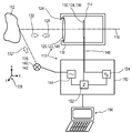
도 1은, 본 발명에 따른 센서 영역을 갖는 종방향 광학 센서를 포함하는 검출기의 예시적인 실시양태를 도시한다.
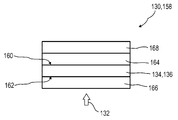
도 2a 및 2b는, 본 발명에 따른 광학 검출기의 종방향 광학 센서의 센서 영역의 2가지 상이한 예시적인 실시양태를 도시한다.
도 3a 내지 3c는, 본 발명에 따른 광학 검출기의 종방향 광학 센서의 센서 영역의 다수의 다른 예시적인 실시양태를 도시한다.
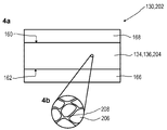
도 4a 및 4b는, 본 발명에 따른 광학 검출기의 종방향 광학 센서의 센서 영역의 다른 예시적인 실시양태를 도시한다.
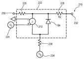
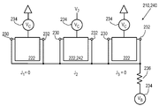
도 5a 내지 5d는, 센서 영역을 나타내기 위한 등가의 회로도를 도시한다.
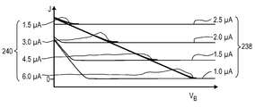
도 6a 및 6b는, 센서 영역에 걸친 바이어스 전압에 대한 "FiP-효과"의 의존성을 보여주는 계산 결과(도 6a) 및 실험 결과(도 6b)를 도시한다.
도 7은, 본 발명에 따른 검출기를 포함하는, 검출기 시스템, 카메라, 인간-기계 인터페이스, 엔터테인먼트 장치 및 추적 시스템의 예시적인 실시양태를 도시한다.
도 8a 및 8b는, 본 발명에 따른 광학 검출기의 종방향 광학 센서의 센서 영역의 다른 예시적인 실시양태를 도시한다.
참조번호 목록
110: 검출기,
112: 물체,
114: 종방향 광학 센서,
116: 광학 축,
118: 하우징,
120: 전달 장치,
122: 굴절 렌즈,
124: 개구,
126: 시인 방향,
128: 좌표계,
130: 센서 영역,
132: 광 빔,
134: 반도체성 물질,
136: 반도체 층,
138: 조명원,
140: 발광 다이오드,
142: 변조된 조명원,
144: 변조 장치,
146: 변조된 전달 장치,
148: 신호 인출선,
150: 평가 장치,
152: 종방향 평가 장치,
154: 바이어스 전압원,
156: 데이터 처리 장치,
158: 제 1 전자 배치,
160: 제 1 표면 영역,
162: 제 2 표면 영역,
164: 고-저항성 층,
166: 제 1 전극,
168: 제 2 전극,
170: 제 2 전자 배치,
172: 분할 전극,
174: 제 1 부분 전극,
176: 제 2 부분 전극,
178: 중-저항성(medium-resistive) 층,
180: 제 3 전자 배치,
182: 다이오드,
184: 다이오드 어레이,
186: n형 반도체성 물질,
188: p형 반도체성 물질,
190: 접합부(p-n 접합),
192: p형 반도체 층,
194: 제 4 전자 배치,
196: 제 5 전자 배치,
198: n형 반도체 층,
200: 절연 패드,
202: 제 6 전자 배치,
204: 비결정질 반도체성 상,
206: 반도체성 입자,
208: 고-저항성 상,
210: 등가 회로,
212: 전류원,
214: 제 1 인출선,
216: 제 2 인출선,
218: 전압계(V),
220: 저항기,
222: 센서 요소,
224: 제어 전압(VC),
226: 저항기,
228: 저항기,
230: 좌측 접촉부,
232: 우측 접촉부,
234: 바이어스 전압(VB),
236: 저항기,
238: 디포커싱된(defocused) 상태,
240: 포커싱된 상태,
242: 중심 센서 요소,
244: 표준화된 광전류(J)의 경로(course),
246: 제 1 초점 값,
248: 제 2 초점 값,
250: 검출기 시스템,
252: 카메라,
254: 인간-기계 인터페이스,
256: 엔터테인먼트 장치,
258: 추적 시스템,
260: 횡방향 광학 센서,
262: 횡방향 평가 유닛,
264: 위치 정보,
266: 이미지화 장치,
268: 제어 요소,
270: 사용자,
272: 비콘(beacon) 장치,
274: 기계,
276: 추적 제어기,
278: 제 7 전자 배치,
280: 절연 층,
282: 다이오드 어레이,
284: 다이오드,
286: p형 반도체성 물질,
288: n형 반도체성 물질,
290: 접합부(p-n 접합),
292: 웰,
294: 고-도전성 층,
296: 측면,
298: 코팅.Other optional details and features of the invention will be apparent from the following description of the preferred exemplary embodiments, which is set forth below in conjunction with the dependent claims. In this context, certain features may be implemented singly or in combination. The present invention is not limited to the exemplary embodiments. Exemplary embodiments are shown diagrammatically in the drawings. Like reference numerals in the individual figures denote like elements or elements having the same function, or elements corresponding to each other of their functions.
Specifically, in the figure,
Figure 1 shows an exemplary embodiment of a detector comprising a longitudinal optical sensor having a sensor region according to the invention.
Figures 2a and 2b show two different exemplary embodiments of the sensor region of a longitudinal optical sensor of an optical detector according to the present invention.
Figures 3A-3C illustrate a number of alternative exemplary embodiments of the sensor region of a longitudinal optical sensor of an optical detector according to the present invention.
4A and 4B show another exemplary embodiment of the sensor area of a longitudinal optical sensor of an optical detector according to the invention.
5A to 5D show equivalent circuit diagrams for indicating sensor regions.
6A and 6B show the calculation results (FIG. 6A) and experimental results (FIG. 6B) showing the dependence of the "FiP-effect" on the bias voltage across the sensor region.
Figure 7 illustrates exemplary embodiments of a detector system, a camera, a human-machine interface, an entertainment device, and a tracking system, including a detector in accordance with the present invention.
8A and 8B illustrate another exemplary embodiment of the sensor region of a longitudinal optical sensor of an optical detector according to the present invention.
Reference number list
110: detector,
112: object,
114: longitudinal optical sensor,
116: optical axis,
118: housing,
120: transmission device,
122: refraction lens,
124: opening,
126: Poetry direction,
128: Coordinate system,
130: sensor area,
132: light beam,
134: semiconducting material,
136: semiconductor layer,
138: Light source,
140: Light emitting diode,
142: Modulated illumination source,
144: modulation device,
146: Modulated transmission device,
148: Signal lead wire,
150: evaluation device,
152: longitudinal direction evaluation device,
154: bias voltage source,
156: Data processing device,
158: first electronic arrangement,
160: first surface area,
162: second surface area,
164: high-resistance layer,
166: a first electrode,
168: second electrode,
170: second electronic arrangement,
172: split electrode,
174: first partial electrode,
176: second partial electrode,
178: a medium-resistive layer,
180: third electronic arrangement,
182: diode,
184: diode array,
186: an n-type semiconductor material,
188: p-type semiconductor material,
190: junction (pn junction),
192: a p-type semiconductor layer,
194: fourth electronic arrangement,
196: fifth electronic arrangement,
198: n-type semiconductor layer,
200: Insulation pad,
202: sixth electronic arrangement,
204: amorphous semiconductor property,
206: semiconductor particles,
208: High-resistance phase,
210: equivalent circuit,
212: current source,
214: first lead wire,
216: second lead line,
218: Voltmeter (V),
220: Resistors,
222: sensor element,
224: control voltage (V C ),
226: Resistors,
228: Resistors,
230: left contact portion,
232: Right contact,
234: Bias voltage (V B ),
236: Resistors,
238: defocused state,
240: focused state,
242: center sensor element,
244: a course of the standardized photocurrent J,
246: first focus value,
248: second focus value,
250: detector system,
252: camera,
254: Human-machine interface,
256: Entertainment device,
258: Tracking system,
260: lateral optical sensor,
262: lateral evaluation unit,
264: location information,
266: Imaging device,
268: control element,
270: User,
272: beacon device,
274: Machinery,
276: tracking controller,
278: seventh electronic arrangement,
280: insulating layer,
282: diode array,
284: diode,
286: p-type semiconductor material,
288: n-type semiconductor material,
290: junction (pn junction),
292: Well,
294: a high-conductive layer,
296: Side,
298: Coating.
이러한 문제들은 본 발명의 특허청구범위의 독립항들에 의해 해결된다. 개별적으로 구현되거나 조합적으로 구현될 수 있는 본 발명의 효과적인 특징들은 종속항 및/또는 아래의 상세한 설명 및 세부 실시양태에 제시된다.These problems are solved by the independent claims of the present invention. The effective features of the present invention, which may be implemented individually or in combination, are set forth in the dependent claims and / or the following detailed description and detailed embodiments.
본원에서 표현 "~을 갖는", "~을 포함하는" 및 "~을 함유하는" 뿐만 아니라 이들의 문법적 변형은 비 배타적인 방식으로 사용된다. 따라서, 표현 "A가 B를 갖는다" 뿐만 아니라 표현 "A가 B를 포함한다" 또는 "A가 B를 함유한다"는 A가 B 이외에도 하나 이상의 다른 구성요소 및/또는 성분을 포함한다는 사실과, B 이외에는 A에 그 어떠한 다른 구성요소, 성분 또는 요소가 제공되지 않는 경우 모두를 지칭할 수 있다.The grammatical variations of the terms "having", "including" and "containing" as well as their grammatical variations are used herein in a non-exclusive manner. Thus, the expression "A contains B" or "A contains B" as well as the expression "A has B" as well as the fact that A includes one or more other components and / B can refer to both, unless A is provided with no other element, component or element.
본 발명의 제 1 양태에서, 광학적 검출을 위한, 특히 하나 이상의 물체의 깊이에 대해 또는 이의 깊이 및 폭 둘 다에 대해 하나 이상의 물체의 위치를 결정하기 위한 검출기가 개시된다.DETAILED DESCRIPTION OF THE INVENTION In a first aspect of the present invention, a detector is disclosed for determining the position of one or more objects for optical detection, particularly for the depth of one or more objects or for both its depth and width.
"물체"는 일반적으로 생명체 및 비-생명체로부터 선택되는 임의의 물체일 수 있다. 따라서, 하나의 예로서, 하나 이상의 물체는 하나 이상의 물품 및/또는 하나의 물품의 하나 이상의 부분을 포함할 수 있다. 추가적으로 또는 대안으로서, 물체는 하나 이상의 생명체 및/또는 생명체의 하나 이상의 부분, 가령 사용자와 같은 인간 및/또는 동물의 하나 이상의 신체 부분일 수 있거나 이를 포함할 수 있다.An "object" may generally be any object selected from living and non-living. Thus, as an example, one or more objects may comprise one or more articles and / or one or more parts of an article. Additionally or alternatively, the object can be or include one or more parts of one or more organisms and / or one or more parts of a living being, such as a human, such as a user, and / or one or more parts of an animal.
본원에서 용어 "위치"는 일반적으로, 물체의 공간적인 위치 및/또는 방향에 대한 정보의 임의의 항목을 지칭한다. 이를 위하여, 하나의 예로서, 하나 이상의 좌표계가 사용될 수 있으며, 물체의 위치는 하나, 둘, 세 개 또는 그보다 많은 좌표들을 사용하여 결정될 수 있다. 하나의 예로서, 하나 이상의 직각 좌표계 및/또는 다른 유형의 좌표계가 사용될 수 있다. 하나의 예에서, 상기 좌표계는, 검출기가 사전결정된 위치 및/또는 방향을 갖는 검출기의 좌표계일 수 있다. 하기에서 더 자세히 설명되는 바와 같이, 상기 검출기는 검출기의 주요 시야 방향을 구성할 수 있는 광학 축을 가질 수 있다. 상기 광학 축은 Z 축과 같은 좌표계의 광학 축을 형성할 수 있다. 또한, 하나 이상의 추가적인 축, 바람직하게는 Z 축에 대해 수직인 축이 제공될 수 있다.The term "location" herein generally refers to any item of information about the spatial location and / or orientation of an object. To this end, as one example, one or more coordinate systems can be used and the position of the object can be determined using one, two, three or more coordinates. As one example, one or more Cartesian and / or other types of coordinate systems may be used. In one example, the coordinate system may be the coordinate system of the detector where the detector has a predetermined position and / or direction. As will be described in more detail below, the detector may have an optical axis that can configure the principal viewing direction of the detector. The optical axis may form an optical axis in the same coordinate system as the Z axis. In addition, one or more additional axes, preferably axes perpendicular to the Z axis, may be provided.
따라서, 하나의 예로서, 검출기는 광학 축이 Z 축을 형성하고 또한 Z 축에 대해 수직인 동시에 서로 수직인 x-축 및 y-축이 제공되는 좌표계를 구성할 수 있다. 하나의 예로서, 검출기 및/또는 검출기의 일부는 좌표계 내의 특정 지점, 가령 좌표계의 원점에 존재할 수 있다. 이러한 좌표계에서, Z 축에 평행하거나 역평행한 방향은 종방향으로서 간주될 수 있으며, Z 축을 따르는 좌표는 종방향 좌표로서 간주될 수 있다. 종방향 좌표에 대해 수직인 임의의 방향은 횡방향으로 간주될 수 있으며 X 좌표 및/또는 Y 좌표가 횡방향 좌표로 간주될 수도 있다.Thus, as an example, the detector may constitute a coordinate system in which the optical axis forms the Z-axis and is perpendicular to the Z-axis and at the same time the x-axis and the y-axis perpendicular to each other are provided. As an example, a portion of the detector and / or detector may be at a particular point in the coordinate system, e.g., at the origin of the coordinate system. In this coordinate system, the direction parallel or anti-parallel to the Z axis can be regarded as the longitudinal direction, and the coordinates along the Z axis can be regarded as the longitudinal coordinates. Any direction perpendicular to the longitudinal coordinate may be regarded as the lateral direction and the X coordinate and / or Y coordinate may be regarded as the lateral coordinate.
다르게는, 다른 유형의 좌표계가 사용될 수도 있다. 따라서, 하나의 예로서, 광학 축이 Z 축을 형성하고 Z 축으로부터의 거리와 편각(polar angle)이 추가적인 좌표로서 사용될 수 있는 극좌표계가 사용될 수도 있다. 또한, Z 축에 대해 평행하거나 역평행한 방향은 종방향으로 간주될 수 있으며, Z 축을 따르는 좌표는 종방향 좌표로 간주될 수도 있다. Z 축에 대해 수직인 임의의 방향은 횡방향으로 간주될 수 있으며 극 좌표 및/또는 편각은 횡방향 좌표로 간주될 수도 있다.Alternatively, other types of coordinate systems may be used. Thus, as an example, a polar coordinate system may be used in which the optical axis forms the Z-axis and the distance from the Z-axis and the polar angle can be used as additional coordinates. Further, the direction parallel or antiparallel to the Z axis may be regarded as the longitudinal direction, and the coordinates along the Z axis may be regarded as the longitudinal direction. Any direction perpendicular to the Z axis may be considered to be transverse, and polar and / or declination angles may be considered to be transverse.
본원에 하나 이상의 물체의 위치를 결정하기 위한 "검출기"는 일반적으로, 하나 이상의 물체의 위치에 대한 하나 이상의 정보 항목을 제공하도록 구성된 장치이다. 상기 검출기는 고정식 장치이거나 이동식 장치일 수 있다. 또한, 상기 검출기는 독립형 장치일 수 있거나 또다른 장치, 가령 컴퓨터, 차량 또는 임의의 다른 장치의 일부일 수 있다. 또한, 상기 검출기는 핸드헬드형 장치일 수 있다. 상기 검출기의 다른 실시양태도 이용가능하다.A "detector" for determining the location of one or more objects herein is generally a device configured to provide one or more information items for the location of one or more objects. The detector may be a stationary device or a mobile device. The detector may also be a stand-alone device or another device, such as a computer, a vehicle or any other device. The detector may also be a handheld device. Other embodiments of the detector are available.
상기 검출기는 하나 이상의 물체의 위치에 대한 하나 이상의 정보 항목을 임의의 실행가능한 방식으로 제공하도록 구성될 수 있다. 따라서, 이러한 정보는 가령 전자적인 방식으로, 시각적인 방식으로, 음향적인 방식으로 또는 이들의 임의의 조합의 방식으로 제공될 수 있다. 이러한 정보는 또한 검출기의 데이터 저장소 또는 별개의 장치에 저장될 수 있고 및/또는 하나 이상의 인터페이스, 가령 무선 인터페이스 및/또는 유선 인터페이스를 통해 제공될 수도 있다.The detector can be configured to provide one or more information items for the location of one or more objects in any executable manner. Thus, such information may be provided, for example, in an electronic manner, in a visual manner, in an acoustic manner, or in any combination of these. This information may also be stored in a data store or a separate device of the detector and / or may be provided via one or more interfaces, such as a wireless interface and / or a wired interface.
본 발명에 따른, 하나 이상의 물체의 광학적 검출을 위한 검출기는 하나 이상의 종방향 광학 센서 및 하나 이상의 평가 장치를 포함하며, 상기 종방향 광학 센서는 하나 이상의 센서 영역을 갖고, 상기 종방향 광학 센서는, 광 빔에 의한 상기 센서 영역의 조사(illumination)에 의존적인 방식으로 하나 이상의 종방향 센서 신호를 생성하도록 설계되고, 상기 종방향 센서 신호는, 상기 조사의 총 전력이 동일하다면, 상기 센서 영역 내의 광 빔의 빔 단면에 대한 의존성을 나타내고, 상기 종방향 센서 신호는, 상기 센서 영역에 포함된 하나 이상의 반도체성 물질에 의해 생성되고, 상기 반도체성 물질의 표면의 일부에 고-저항성 물질이 존재하고, 상기 고-저항성 물질은 상기 반도체성 물질의 전기 저항과 동등하거나 이를 초과하는 전기 저항을 나타내고, 상기 평가 장치는, 상기 종방향 광학 센서의 종방향 센서 신호를 평가함으로써 물체의 종방향 위치에 대한 하나 이상의 정보 항목을 생성하도록 설계된다.According to the present invention, a detector for optical detection of at least one object comprises at least one longitudinal optical sensor and at least one evaluation device, the longitudinal optical sensor having at least one sensor region, Wherein the sensor is designed to generate at least one longitudinal sensor signal in a manner dependent on illumination of the sensor region by a light beam, Wherein the longitudinal sensor signal is indicative of a dependence of the beam on the beam cross-section, the longitudinal sensor signal being generated by at least one semiconducting material contained in the sensor region, Wherein the high -resistance material exhibits electrical resistance equal to or greater than the electrical resistance of the semiconductive material, The device is designed to generate one or more items of information on the longitudinal position of the object by evaluating the longitudinal sensor signal of the longitudinal optical sensor.
본원에서, 상기 열거된 구성요소는 별도의 구성요소일 수 있다. 다르게는, 위에서 열거된 바와 같은 구성요소들 중 둘 이상이 단일 구성요소로 통합될 수 있다. 더욱이, 하나 이상의 평가 장치는 전송 장치 및 종방향 광학 센서와는 독립적인 분리된 평가 장치로서 형성될 수 있지만, 바람직하게는, 종방향 센서 신호를 수신하기 위해 종방향 광학 센서에 접속될 수 있다. 다르게는, 하나 이상의 평가 장치는 종방향 광학 센서 내에 완전히 또는 부분적으로 통합될 수 있다.In the present application, the above listed components may be separate components. Alternatively, two or more of the components listed above may be integrated into a single component. Furthermore, the at least one evaluation device may be formed as a separate evaluation device independent of the transmission device and the longitudinal optical sensor, but may preferably be connected to the longitudinal optical sensor to receive the longitudinal sensor signal. Alternatively, the one or more evaluation devices may be fully or partially integrated into the longitudinal optical sensor.
본원에서 "종방향 광학 센서"는, 일반적으로 광 빔에 의한 센서 영역의 조사에 의존적인 방식으로 하나 이상의 종방향 센서 신호를 생성하도록 설계되는 장치이고, 종방향 센서 신호는, 상기 조사의 총 전력이 동일하다면, "FiP-효과"에 따라, 센서 영역에서의 광 빔의 빔 단면에 의존적이다. 일반적으로, 종방향 센서 신호는 깊이로서 표기될 수도 있는 종방향 위치를 나타내는 임의의 신호일 수 있다. 예로서, 종방향 센서 신호는 디지털 및/또는 아날로그 신호이거나 또는 이를 포함할 수 있다. 예로서, 종방향 센서 신호는 전압 신호 및/또는 전류 신호이거나 또는 이를 포함할 수 있다. 추가적으로 또는 다르게는, 종방향 센서 신호는 디지털 데이터이거나 또는 이를 포함할 수 있다. 종방향 센서 신호는 단일의 신호 값 및/또는 일련의 신호 값들을 포함할 수 있다. 종방향 센서 신호는 둘 이상의 신호를 평균화 및/또는 둘 이상의 신호의 몫(quotient)을 형성하는 것과 같이, 둘 이상의 개별적인 신호를 조합하여 도출되는 임의의 신호를 더 포함할 수 있다. 종방향 광학 센서 및 종방향 센서 신호의 잠재적인 실시양태의 경우, 국제 특허 출원 공개 제 WO 2012/110924 A1 호 또는 제 WO 2014/097181 A1 호에 개시된 바와 같은 광학 센서를 참조할 수 있다.As used herein, a "longitudinal optical sensor" is a device designed to generate one or more longitudinal sensor signals in a manner that is generally dependent on the irradiation of the sensor region by the light beam, Is the same, it depends on the beam cross-section of the light beam in the sensor region, according to the "FiP-effect ". In general, the longitudinal sensor signal may be any signal that represents a longitudinal position that may be denoted as a depth. By way of example, the longitudinal sensor signal may be or include digital and / or analog signals. By way of example, the longitudinal sensor signal may be or include a voltage signal and / or a current signal. Additionally or alternatively, the longitudinal sensor signal may be or include digital data. The longitudinal sensor signal may comprise a single signal value and / or a series of signal values. The longitudinal sensor signal may further include any signal derived by combining two or more separate signals, such as averaging two or more signals and / or forming a quotient of two or more signals. For potential embodiments of longitudinal optical sensors and longitudinal sensor signals, reference may be made to optical sensors as disclosed in International Patent Application Publication No. WO 2012/110924 Al or WO 2014/097181 A1.
여기에서, 하나 이상의 종방향 광학 센서는 하나 이상의 센서 영역을 나타내고, 상기 센서 영역은 하나 이상의 반도체성 물질을 포함하고, 상기 반도체성 물질은, 단일-상 물질 또는 반도체성 물질의 2개 이상, 바람직하게는 2개 또는 3개의 개별적인 상을 포함할 수 있다. 또한, 본원에서 용어 "상"은, 물질의 한정된 부피 또는 이의 일부 내의 균질한 조성을 지칭할 수 있다. 여기에서, 한정된 부피는, 예를 들어 벌크 물질 형태 또는 다공성 물질 형태의 일체성(coherent) 배열을 나타낼 수 있으며, 이때 공극은, 각각 제 2 물질, 예를 들어 추가의 반도체성 물질; 저-저항성 물질, 예컨대 금속성 전도성 물질; 고-저항성 물질, 예컨대 절연 물질; 또는 유체, 예컨대 기체 또는 액체 조성물을 나타낼 수 있는 하나 이상의 추가의 상을 포함할 수 있다. 대안적으로 또는 추가적으로, 상기 부피는, 예를 들어, 전술된 바와 같은 제 2 물질 중 하나를 각각 포함할 수 있는 하나 이상의 추가의 상에 의해 분리될 수 있는 개별 부피를 형성함으로써, 비-간섭성(incoherent) 배열을 나타낼 수 있다. 바람직하게는, 상기 반도체성 물질은 외인성 반도체를 포함할 수 있으며, 이때 상기 반도체성 물질의 전자 특성은 도핑제를 도입함으로써 변경되어, 반도체성 물질 내의 전하 캐리어 농도가 영향을 받게 된다. 따라서, 최신 기술로부터 공지된 바와 같이, 상기 반도체성 물질은, 전하 캐리어가 주로 전자에 의해 제공되는 n형 반도체성 물질; 또는 전하 캐리어가 정공에 의해 주로 제공되는 p형 반도체성 물질로부터 선택될 수 있다. 또한, 도핑되지 않은 진성 i형 반도체성 물질이 여전히 n형 반도체성 물질과 p형 반도체성 물질 사이에 위치될 수 있다. 그러나, 다른 배열이 가능할 수 있다.Wherein the at least one longitudinal optical sensor represents at least one sensor region and wherein the sensor region comprises at least one semiconducting material and wherein the semiconducting material comprises at least two of a single- May comprise two or three separate phases. The term "phase" herein may also refer to a homogeneous composition within a defined volume of a material or a portion thereof. Herein, the defined volume may represent, for example, a coherent arrangement in the form of a bulk material or a porous material, where the pores each comprise a second material, for example a further semiconductive material; Low-resistance materials, such as metallic conductive materials; A high-resistance material such as an insulating material; Or a fluid, such as a gas or liquid composition. Alternatively or additionally, the volume can be reduced by forming individual volumes that can be separated by, for example, one or more additional phases, each of which may include one of the second materials as described above, (incoherent) array. Preferably, the semiconducting material may comprise an extrinsic semiconductor, wherein the electronic properties of the semiconducting material are altered by introducing a dopant, whereby the charge carrier concentration in the semiconducting material is affected. Thus, as is known from the state of the art, the semiconducting material comprises an n-type semiconducting material in which the charge carrier is mainly provided by electrons; Or a p-type semiconducting material in which a charge carrier is predominantly provided by holes. Also, undoped intrinsic i-type semiconducting material may still be located between the n-type semiconducting material and the p-type semiconducting material. However, other arrangements may be possible.
일반적으로, 상기 반도체성 물질은, 전형적으로 10-6 S/m 내지 103 S/m의 값을 갖는 전기 전도도(즉, 금속성 물질의 전도도(103 S/m 이상, 특히 106 S/m 이상)와 절연 물질의 전도도(10-6 S/m 미만, 특히 10-8 S/m 이하) 사이)를 나타낸다. 이로써, 전기 전도도 값은, 상기 반도체성 물질의 전류 운반 능력을 결정한다. 특히, 상기 반도체성 물질과 관련하여, 전기 전도도는 일반적으로 전하 캐리어의 개수에 의존하며, 이때 전하 캐리어의 개수는 물질의 유형뿐만 아니라 상기 물질 내로 삽입되는 도판트의 유형에 의존한다. 또한, 본원에서 특정 물질의 "전기 저항"은, 전기 전도도의 역수 값을 나타낸다. 따라서, 상기 센서 영역 내의 반도체성 물질은 전기 저항에 대한 특정 값을 나타낸다. Typically, the semiconducting material has an electrical conductivity (i.e., a conductivity of at least 10 3 S / m, in particular 10 6 S / m, typically 10 6 S / m to 10 3 S / Or more) and the conductivity of the insulating material (less than 10 -6 S / m, especially 10 -8 S / m or less). As such, the electrical conductivity value determines the current carrying capacity of the semiconductive material. In particular, with respect to the semiconducting material, the electrical conductivity generally depends on the number of charge carriers, wherein the number of charge carriers depends on the type of material as well as the type of dopant to be inserted into the material. In addition, the term "electrical resistance" of a specific substance in the present application represents an inverse value of electrical conductivity. Thus, the semiconducting material in the sensor region represents a specific value for electrical resistance.
본 발명의 목적을 위해, 상기 종방향 광학 센서의 센서 영역 내에 포함된 반도체성 물질은 바람직하게는 무기 반도체성 물질, 유기 반도체성 물질 또는 이들의 조합물을 포함할 수 있다.For purposes of the present invention, the semiconducting material contained within the sensor region of the longitudinal optical sensor may preferably comprise an inorganic semiconducting material, an organic semiconducting material, or a combination thereof.
이와 관련하여, 상기 무기 반도체성 물질은 특히, 하나 이상의 셀루륨, 텔루륨, 셀루륨-텔루륨 합금, 금속 옥사이드, IV족 원소 또는 화합물, 즉, IV족으로부터의 원소, 또는 하나 이상의 IV족 원소를 갖는 화학적 화합물, III-V 화합물, 즉, 하나 이상의 III족 원소와 하나 이상의 V족 원소를 갖는 화학적 화합물, II-VI 화합물, 즉, 하나 이상의 II족 원소 및 하나 이상의 VI족 원소를 갖는 화학적 화합물, 및/또는 칼코게나이드 중 적어도 하나를 포함할 수 있다. 그러나, 다른 무기 반도체성 물질도 동등하게 적절할 수 있다.In this regard, the inorganic semiconducting material is particularly preferably one or more elements selected from the group consisting of one or more of the group consisting of a cellulosium, a tellurium, a cellulo-tellurium alloy, a metal oxide, a group IV element or a compound, A chemical compound having at least one Group III element and at least one Group V element, a chemical compound having at least one Group II element and at least one Group VI element, a chemical compound having at least one Group III element and at least one Group V element, , ≪ / RTI > and / or chalcogenide. However, other inorganic semiconducting materials may be equally suitable.
이와 관련하여, 상기 무기 반도체성 물질은 특히, 하나 이상의 셀루륨, 텔루륨, 셀루륨-텔루륨 합금, 금속 옥사이드, IV족 원소 또는 화합물, 즉, IV족으로부터의 원소, 또는 하나 이상의 IV족 원소를 갖는 화학적 화합물, III-V 화합물, 즉, 하나 이상의 III족 원소와 하나 이상의 V족 원소를 갖는 화학적 화합물, II-VI 화합물, 즉, 하나 이상의 II족 원소 및 하나 이상의 VI족 원소를 갖는 화학적 화합물, 및/또는 칼코게나이드 중 적어도 하나를 포함할 수 있다. 그러나, 다른 무기 반도체성성 물질도 동등하게 적절할 수 있다.In this regard, the inorganic semiconducting material is particularly preferably one or more elements selected from the group consisting of one or more of the group consisting of a cellulosium, a tellurium, a cellulo-tellurium alloy, a metal oxide, a group IV element or a compound, A chemical compound having at least one Group III element and at least one Group V element, a chemical compound having at least one Group II element and at least one Group VI element, a chemical compound having at least one Group III element and at least one Group V element, , ≪ / RTI > and / or chalcogenide. However, other inorganic semiconducting materials may be equally suitable.
상기 금속 옥사이드와 관련하여, 이러한 종류의 반도체성 물질은, 구리(II) 옥사이드(CuO), 구리(I) 옥사이드(CuO2), 니켈 옥사이드(NiO), 아연 옥사이드(ZnO), 은 옥사이드(Ag2O), 망간 옥사이드(MnO), 티타늄 다이옥사이드(TiO2), 바륨 옥사이드(BaO), 납 옥사이드(PbO), 세륨 옥사이드(CeO2), 비스무트 옥사이드(Bi2O3), 및 카드뮴 옥사이드(CdO)를 포함하는 군으로부터 선택될 수 있다. 다른 3상, 4상 또는 그보다 많은 상의 금속 옥사이드 역시 적용가능할 수 있다. In relation to the metal oxide, this type of semiconductor material, copper (II) oxide (CuO), copper (I) oxide (CuO 2), nickel oxide (NiO), zinc oxide (ZnO), the oxide (Ag 2 O), manganese oxide (MnO), titanium dioxide (TiO 2), barium oxide (BaO), lead oxide (PbO), cerium oxide (CeO 2), bismuth oxide (Bi 2 O 3), and cadmium oxide (CdO ). ≪ / RTI > Other three-phase, four-phase, or more phase metal oxides may also be applicable.
IV족 원소 또는 화합물과 관련하여, 이러한 종류의 반도체성 물질은, 도핑된 다이아몬드(C), 도핑된 규소(Si), 규소 카바이드(SiC), 및 규소 게르마늄(SiGe)을 포함하는 군으로부터 선택될 수 있다.With respect to Group IV elements or compounds, this type of semiconducting material is selected from the group comprising doped diamond (C), doped silicon (Si), silicon carbide (SiC), and silicon germanium (SiGe) .
III-V 화합물과 관련하여, 이러한 종류의 반도체성 물질은, 인듐 안티모나이드(InSb), 붕소 나이트라이드(BN), 붕소 포스파이드(BP), 붕소 아르세나이드(BAs), 알루미늄 나이트라이드(AlN), 알루미늄 포스파이드(AlP), 알루미늄 아르세나이드(AlAs), 알루미늄 안티모나이드(AlSb), 인듐 나이트라이드(InN), 인듐 포스파이드(InP), 인듐 아르세나이드(InAs), 인듐 안티모나이드(InSb), 갈륨 나이트라이드(GaN), 갈륨 포스파이드(GaP), 갈륨 아르세나이드(GaAs), 및 갈륨 안티모나이드(GaSb)를 포함하는 군으로부터 선택될 수 있다.With respect to the III-V compounds, this type of semiconducting material can be formed by a combination of indium antimonide (InSb), boron nitride (BN), boron phosphide (BP), boron arsenide (BAs), aluminum nitride AlN), aluminum phosphide (AlP), aluminum arsenide (AlAs), aluminum antimonide (AlSb), indium nitride (InN), indium phosphide (InP), indium arsenide May be selected from the group comprising monad (InSb), gallium nitride (GaN), gallium phosphide (GaP), gallium arsenide (GaAs), and gallium antimonide (GaSb).
II-VI 화합물과 관련하여, 이러한 종류의 반도체성 물질은, 카드뮴 설파이드(CdS), 카드뮴 셀레나이드(CdSe), 카드뮴 텔루라이드(CdTe), 아연 설파이드(ZnS), 아연 셀레나이드(ZnSe), 아연 텔루라이드(ZnTe), 수은 설파이드(HgS), 수은 셀레나이드(HgSe), 수은 텔루라이드(HgTe), 카드뮴 아연 텔루라이드(CdZnTe), 수은 카드뮴 텔루라이드(HgCdTe), 수은 아연 텔루라이드(HgZnTe), 및 수은 아연 셀레나이드(CdZnSe)를 포함하는 군으로부터 선택될 수 있다. 그러나, 다른 II-VI 화합물도 가능할 수 있다.With respect to II-VI compounds, this type of semiconducting material can be selected from the group consisting of cadmium sulfide (CdS), cadmium selenide (CdSe), cadmium telluride (CdTe), zinc sulfide (ZnS), zinc selenide Mercury mercury telluride (HgSe), mercury telluride (HgTe), cadmium zinc telluride (CdZnTe), mercury cadmium telluride (HgCdTe), mercury zinc telluride (HgZnTe), mercury cadmium telluride And mercury zinc selenide (CdZnSe). However, other II-VI compounds may also be possible.
칼코게나이드와 관련하여, 이러한 종류의 반도체성 물질은, 적합한 반도체성 특성을 나타내는 한, 설파이드 칼코게나이드, 셀레나이드 칼코게나이드, 텔루라이드 칼코게나이드, 3상 칼코게나이드, 4상 및 그보다 많은 상의 칼코게나이드를 포함하는 군으로부터 선택될 수 있다. With respect to chalcogenide, this type of semiconducting material can be selected from the group consisting of sulfide chalcogenide, selenide chalcogenide, telluride chalcogenide, 3-phase chalcogenide, 4-phase and more Many phases can be selected from the group comprising chalcogenides.
특히, 설파이드 칼코게나이드는, 납 설파이드(PbS), 카드뮴 설파이드(CdS), 아연 설파이드(ZnS), 수은 설파이드(HgS), 은 설파이드(Ag2S), 망간 설파이드(MnS), 비스무트 트라이설파이드(Bi2S3), 안티몬 트라이설파이드(Sb2S3), 비소 트라이설파이드(As2S3), 주석(II) 설파이드(SnS), 주석(IV) 다이설파이드(SnS2), 인듐 설파이드(In2S3), 구리 설파이드(CuS 또는 Cu2S), 코발트 설파이드(CoS), 니켈 설파이드(NiS), 몰리브덴 다이설파이드(MoS2), 철 다이설파이드(FeS2), 및 크롬 트라이설파이드(CrS3)를 포함하는 군으로부터 선택될 수 있다. In particular, the sulfide chalcogenide is a mixture of lead sulfide (PbS), cadmium sulfide (CdS), zinc sulfide (ZnS), mercury sulfide (HgS), silver sulfide (Ag 2 S), manganese sulfide (MnS), bismuth tri- ssulfide Bi 2 S 3 ), antimony triisulfide (Sb 2 S 3 ), arsenic tri-sulphide (As 2 S 3 ), tin (II) sulfide (SnS), tin (IV) disulfide (SnS 2 ) 2 S 3), copper sulfide (CuS or Cu 2 S), cobalt sulphide (CoS), nickel sulfide (NiS), molybdenum disulfide (MoS 2), iron disulfide (FeS 2), and chromium tri-sulfide (CrS 3 ). ≪ / RTI >
특히, 셀레나이드 칼코게나이드는, 납 셀레나이드(PbSe), 카드뮴 셀레나이드(CdSe), 아연 셀레나이드(ZnSe), 비스무트 트라이셀레나이드(Bi2Se3), 수은 셀레나이드(HgSe), 안티몬 트라이셀레나이드(Sb2Se3), 비소 트라이셀레나이드(As2Se3), 니켈 셀레나이드(NiSe), 탈륨 셀레나이드(TlSe), 구리 셀레나이드(CuSe 또는 Cu2Se), 몰리브덴 다이셀레나이드(MoSe2), 주석 셀레나이드(SnSe), 및 코발트 셀레나이드(CoSe), 및 인듐 셀레나이드(In2Se3)를 포함하는 군으로부터 선택될 수 있다.In particular, selenide chalcogenide is, lead-selenide (PbSe), cadmium selenide (CdSe), zinc selenide (ZnSe), bismuth tri-selenide (Bi 2 Se 3), mercury selenide (HgSe), antimony tri (Sb 2 Se 3 ), arsenic triacenide (As 2 Se 3 ), nickel selenide (NiSe), thallium selenide (TlSe), copper selenide (CuSe or Cu 2 Se), molybdenum diselenide MoSe 2 ), tin selenide (SnSe), and cobalt selenide (CoSe), and indium selenide (In 2 Se 3 ).
특히, 텔루라이드 칼코게나이드는, 납 텔루라이드(PbTe), 카드뮴 텔루라이드(CdTe), 아연 텔루라이드(ZnTe), 수은 텔루라이드(HgTe), 비스무트 트라이텔루라이드(Bi2Te3), 비소 트라이텔루라이드(As2Te3), 안티몬 트라이텔루라이드(Sb2Te3), 니켈 텔루라이드(NiTe), 탈륨 텔루라이드(TlTe), 구리 텔루라이드(CuTe), 몰리브덴 다이텔루라이드(MoTe2), 주석 텔루라이드(SnTe), 및 코발트 텔루라이드(CoTe), 은 텔루라이드(Ag2Te), 및 인듐 텔루라이드(In2Te3)를 포함하는 군으로부터 선택될 수 있다. In particular, telluride chalcogenide is, lead telluride (PbTe), cadmium telluride (CdTe), zinc telluride (ZnTe), mercury telluride (HgTe), bismuth tri-telluride (Bi 2 Te 3), arsenic tri telluride (As 2 Te 3), antimony tri-telluride (Sb 2 Te 3), nickel telluride (NiTe), thallium telluride (TlTe), copper telluride (CuTe), molybdenum die telluride (MoTe 2), Tin telluride (SnTe), and cobalt telluride (CoTe), silver telluride (Ag 2 Te), and indium telluride (In 2 Te 3 ).
특히, 3상 칼코게나이드는, 수은 카드뮴 텔루라이드(HgCdTe; MCT), 수은 아연 텔루라이드(HgZnTe), 수은 카드뮴 설파이드(HgCdS), 납 카드뮴 설파이드(PbCdS), 납 수은 설파이드(PbHgS), 구리 인듐 다이설파이드(CuInS2; CIS), 카드뮴 설포셀레나이드(CdSSe), 아연 설포셀레나이드(ZnSSe), 탈륨 설포셀레나이드(TlSSe), 카드뮴 아연 설파이드(CdZnS), 카드뮴 크롬 설파이드(CdCr2S4), 수은 크롬 설파이드(HgCr2S4), 구리 크롬 설파이드(CuCr2S4), 카드뮴 납 셀레나이드(CdPbSe), 구리 인듐 다이셀레나이드(CuInSe2), 인듐 갈륨 아르세나이드(InGaAs), 납 옥사이드 설파이드(Pb2OS), 납 옥사이드 셀레나이드(Pb2OSe), 납 설포셀레나이드(PbSSe), 비소 셀레나이드 텔루라이드(As2Se2Te), 인듐 갈륨 포스파이드(InGaP), 갈륨 아르세나이드 포스파이드(GaAsP), 알루미늄 갈륨 포스파이드(AlGaP), 카드뮴 셀레나이트(CdSeO3), 카드뮴 아연 텔루라이드(CdZnTe), 및 카드뮴 아연 셀레나이드(CdZnSe), 상기 열거된 2상 칼코게나이드 및/또는 2상 III족-V족-화합물로부터의 화합물을 적용함으로써 수득된 추가의 조합물을 포함하는 군으로부터 선택될 수 있다.Particularly, the three-phase chalcogenide is selected from the group consisting of mercury cadmium telluride (HgCdTe; MCT), mercury zinc telluride (HgZnTe), mercury cadmium sulfide (HgCdS), lead cadmium sulfide (PbCdS), lead mercury sulfide (PbHgS) disulfide (CuInS 2; CIS), cadmium sulfo-selenide (CdSSe), zinc sulfo-selenide (ZnSSe), thallium sulfo-selenide (TlSSe), cadmium zinc sulfide (CdZnS), cadmium, chromium sulfide (CdCr 2 S 4), mercury, chromium sulfide (HgCr 2 S 4), copper chromium sulfide (CuCr 2 S 4), cadmium, lead selenide (CdPbSe), copper indium di-selenide (CuInSe 2), indium gallium arsenide (InGaAs), lead oxide, sulfide (Pb 2 OS), lead oxide selenide (Pb 2 OSe), lead sulfoselenide (PbSSe), arsenic selenide telluride (As 2 Se 2 Te), indium gallium phosphide (InGaP) (GaAsP), aluminum gallium phosphide (AlGaP), cadmium cell By applying the compounds from compound-les nitro (CdSeO 3), cadmium zinc telluride (CdZnTe), and cadmium zinc selenide (CdZnSe), recited above the two-phase chalcogenide and / or group 2, the group III -V ≪ / RTI > and additional combinations obtained.
다르게는 또는 추가적으로, 상기 유기 반도체성 물질은 특히, 프탈로시아닌, 나프탈로시아닌, 서브프탈로시아닌, 페릴렌, 안트라센, 피렌, 올리고- 및 폴리티오펜, 풀러렌, 인디고이드 염료, 비스-아조 안료, 스쿠아릴륨 염료, 티아피릴륨 염료, 아줄레늄 염료, 다이티오케토-피롤로피롤, 퀸아크리돈, 다이브로모안탄트론, 폴리비닐카바졸, 및 이들의 유도체 및 조합물로 이루어진 군으로부터 선택되는 반도체성 화합물일 수 있거나 이를 포함할 수 있다.Alternatively or additionally, the organic semiconducting material may be selected from the group consisting of phthalocyanine, naphthalocyanine, subphthalocyanine, perylene, anthracene, pyrene, oligo- and polythiophene, fullerene, indigoid dyes, bis-azo pigments, squarylium dyes , Thiapyrilium dyes, azulenium dyes, dithioceto-pyrrolopyrroles, quinacridones, dibromoanthanthrone, polyvinylcarbazole, and derivatives and combinations thereof. Or may include the same.
또한, 2016 년 1월 28일자로 출원된 국제 특허 출원 제 PCT/EP2016/051817 호는, 본 발명의 목적에 동등하게 적용될 수 있는 다수의 반도체성 물질을 개시하고 있으며, 상기 출원의 전체 내용을 본원에 참고로 인용한다.International Patent Application No. PCT / EP2016 / 051817, filed January 28, 2016, discloses a number of semiconducting materials which may equally be applied for the purposes of the present invention, Quot;
또한, 상기 반도체성 물질을 포함하는 상기 종방향 광학 센서의 센서 영역은 하나 이상의 광 빔에 의해 조사된다(illuminated). 따라서, 상기 조사의 총 전력이 동일하다면, 상기 센서 영역 내의 반도체성 물질 내의 광전류는, 상기 센서 영역 내의 광 빔의 빔 단면(이는, 상기 센서 영역 내의 입사 빔에 의해 생성되는 "스팟 크기"로서 명명)에 의존적이다. 따라서, 입사 광 빔에 의한, 상기 반도체성 물질을 포함하는 상기 센서 영역의 조사 정도에 상기 반도체성 물질 내의 광전류가 의존적이라는 관찰가능한 특성은 특히, 동일한 총 전력을 포함하지만 상기 센서 영역 상에 상이한 스팟 크기를 생성하는 2개의 광 빔이 상기 센서 영역 내의 반도체성 물질의 광전류의 상이한 값을 제공하고 동시에 서로에 대해 구별가능함을 달성한다.In addition, the sensor region of the longitudinal optical sensor comprising the semiconductive material is illuminated by one or more light beams. Thus, if the total power of the irradiation is the same, the photocurrent in the semiconducting material in the sensor region will have a beam cross section of the light beam in the sensor region, which is named "spot size" generated by the incident beam in the sensor region. ). Thus, the observable characteristic that the photocurrent in the semiconducting material depends on the degree of irradiation of the sensor region comprising the semiconductive material by the incident light beam, in particular, includes the same total power, Achieves that the two light beams producing the magnitude provide different values of the photocurrent of the semiconducting material in the sensor region and at the same time are distinguishable from each other.
일반적으로, 센서 영역 내의 광전류는, 전술된 바와 같이 반도체성 물질 내에서 이용가능한 전하 캐리어에 기인할 수 있다고 가정된다. 센서 영역 내의 반도체성 물질 내의 하나 이상의 광전류 값을 실제로 결정할 수 있도록, 상기 반도체성 물질은 바람직하게는 2개 이상의 전극 사이에 함입될 수 있으며, 상기 전극은 특히, 내부의 전하 캐리어에 대한 높은 전도도를 제공하기 위해 상기 반도체성 물질의 전기 전도도의 값보다 높은 전기 전도도를 나타낸다. 결과적으로, 하나 이상의 광전류 값은, 전극을 사용하여 센서 영역 또는 이의 일부에 걸쳐 하나 이상의 전류 또는 전압을 측정함으로써 획득될 수 있다. 이를 위해, 전기장은 센서 영역 내의 반도체성 물질의 적어도 일부에 걸쳐 적용되고/되거나 생성될 수 있다. 이로써, 하나 이상의 광전류 값에 기초한, 광학 검출기에 의해 생성된 종방향 센서 신호의 하나 이상의 값이 수득될 수 있다. It is generally assumed that the photocurrent in the sensor region can be attributed to the charge carriers available in the semiconductive material, as described above. The semiconducting material may preferably be sandwiched between two or more electrodes so that one or more photocurrent values in the semiconducting material in the sensor region can actually be determined, said electrode particularly having a high conductivity for the internal charge carrier Exhibits a higher electrical conductivity than the value of the electrical conductivity of the semiconducting material. As a result, one or more photocurrent values can be obtained by measuring one or more currents or voltages across the sensor region or a portion thereof using an electrode. To this end, the electric field can be applied and / or produced over at least a portion of the semiconducting material in the sensor region. Thereby, one or more values of the longitudinal sensor signal generated by the optical detector, based on one or more photocurrent values, can be obtained.
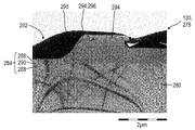
상기 광 빔이 센서 영역 내의 반도체성 물질 상에 충돌하도록, 바람직하게는, 상기 전극들 중 적어도 하나가 입사 광 빔의 파장에 대해 투명할 수 있다. 따라서, 투명 전극은 전기 전도성 투명 물질, 바람직하게는 투명한 전도성 옥사이드, 특히 인듐 주석 옥사이드(ITO 또는 주석-도핑된 인듐 옥사이드), 즉 인듐(III) 옥사이드와 주석(IV) 옥사이드(SnO2)의 고용체(예컨대, 90 중량%의 In2O3 및 10 중량%의 SnO2)를 포함하며, 이는 종래 기술에 따라 높은 전기 전도도를 포함한다. 동시에, ITO는 380nm 내지 780nm의 가시 스펙트럼 범위에서 얇은 층으로는 투명하고 무색이지만, 적외선(IR) 스펙트럼 범위와 자외선(UV) 스펙트럼 범위 둘 다에서는 불투명 한 특성을 나타내는 것으로 공지되어 있다. 그러나, 가시광 스펙트럼 범위에서는, 다른 투명 전극 물질, 예를 들어 불소 주석 옥사이드(SnO2:F 또는 FTO), 알루미늄 아연 옥사이드(ZnO:Al 또는 AZO), 안티몬 주석 옥사이드(SnO2:Sb 또는 ATO), 또는 그래핀이 사용될 수 있다. 그러나 다른 스펙트럼 범위의 경우, 다른 물질이 적합할 수 있다.Preferably, at least one of the electrodes is transparent to the wavelength of the incident light beam such that the light beam impinges on the semiconductive material in the sensor region. Thus, the transparent electrode is an electrically conductive transparent material, preferably a transparent conductive oxide, in particular indium tin oxide (ITO, or tin-doped indium oxide), or a solid solution of indium (III) oxide and tin (IV) oxide (SnO 2) (E. G., 90% by weight of In 2 O 3 and 10% by weight of SnO 2 ), which comprises high electrical conductivity according to the prior art. At the same time, ITO is known to be opaque in both the infrared (IR) spectral range and the ultraviolet (UV) spectral range, although it is transparent and colorless as a thin layer in the visible spectrum range of 380 nm to 780 nm. However, in the visible spectral range, and the other transparent electrode material, for example, fluorine tin oxide (SnO 2: F, or FTO), aluminum zinc oxide (ZnO: Al or AZO), antimony tin oxide (SnO 2: Sb, or ATO), Or graphene may be used. However, for other spectral ranges, other materials may be suitable.
본 발명에 따르면, 상기 반도체성 물질은, 상기 센서 영역 내에 반도체성 물질의 표면의 일부가, 상기 반도체성 물질의 상에 대해 결정된 전기 정항 값과 적어도 동일하거나 바람직하게는 이를 초과할 수 있는 전기 저항 값을 경험할 수 있는 방식으로, 상기 센서 영역 내에 배열된다. 본 발명에 따르면, 이러한 종류의 배열은, 반도체성 물질의 표면의 일부에 존재하는 고-저항성 물질을 제공함으로써 달성된다. 본원에서 용어 "고-저항성 물질"은, 고-저항성 물질에 인접하여 위치하는 반도체성 물질의 전기 저항과 적어도 동일하거나 바람직하게는 이를 초과하는 전기 저항을 나타내지만, 상기 정의된 바와 같은 절연 물질을 구성하지 않는 물질을 지칭한다. 이와 관련하여, 반도체성 물질의 표면에 도달할 수 있는 전하 캐리어가 고-저항성 물질과 마주 칠 수 있는 것이 특히 충분할 수 있으며, 이때 고-저항성 물질은 바람직하게는 반도체성 물질과 상이할 수 있지만, 다르게는, 고-저항성 물질이 경계, 계면 및/또는 접합부에 의해 반도체성 물질로부터 적어도 분리될 수 있는 한, 심지어 동일한 종류의 반도체성 물질를 포함할 수 있다. 본원에서 용어 "경계", "계면" 및 "접합부"는, 관련된 물질, 즉, 경계, 계면 및/또는 접합부 중 적어도 두 면에 위치하는 반도체성 물질 및 고-전도성 물질의 스케일링 거동을 지칭할 수 있다. 여기에서, 특히, 관련 물질의 경계, 계면 및/또는 접합부 내에서 발생하는 스케일링 거동은, 이의 전기 전도성 특성 값의 변화를 포함한다. 이론상, 스케일링 거동은 비-연속적 함수에 의해 기술될 수 있지만, 실제 경계, 계면 및/또는 접합부에서는 항상 연속적 전이가 관찰될 수 있다.According to the present invention, the semiconducting material is characterized in that a part of the surface of the semiconducting material in the sensor area has an electrical resistance which may be at least equal to or preferably greater than the electrical setting value determined for the phase of the semiconducting material Values in the sensor region. According to the present invention, this kind of arrangement is achieved by providing a high-resistance material present in a part of the surface of the semiconducting material. As used herein, the term "high-resistance material" refers to an electrical resistance that is at least equal to or preferably greater than the electrical resistance of a semiconducting material located adjacent a high-resistance material, Refers to materials that do not constitute. In this regard, it may be particularly sufficient that the charge carriers capable of reaching the surface of the semiconducting material can be faced with a high-resistive material, wherein the high-resistive material is preferably different from the semiconducting material, Alternatively, as long as the high-resistance material can be at least separated from the semiconducting material by the interface, interface and / or junction, it may even comprise the same type of semiconducting material. The terms "boundary "," interface ", and "junction" herein may refer to the scaling behavior of the semiconducting material and the high-conductivity material that are located on at least two of the related materials, have. Here, in particular, the scaling behavior that occurs within the boundaries, interfaces and / or junctions of the relevant materials involves a change in its electrical conductivity characteristic value. In theory, the scaling behavior can be described by a non-continuous function, but continuous transitions can always be observed at the actual boundary, interface and / or junction.
특히, 반도체성 물질과 고-저항성 물질 사이의 경계, 계면 및/또는 접합부 내에서의 저항 거동은 비선형 형태를 포함할 수 있다. 따라서, 바람직한 실시양태에서, 반도체성 물질과 고-저항성 물질 사이의 경계, 계면 및/또는 접합부 내에서의 전기 저항의 비선형 거동은, 초점 스팟 직경에 대한 광전류의 선형 의존성을 야기하도록 조정될 수 있다. 따라서, 하기에 더욱 상세히 설명되는 바와 같이, 고-저항성 물질은 다수의 상이한 형태를 취할 수 있으며, 특히, 고-저항성 층, 고-저항성 코팅, 고-저항성 공핍 대역, 고-저항성 터널링 장벽, 고-저항성 밴드-대-밴드 계면, 및 고-저항성 쇼트키 장벽 중 적어도 하나로부터 선택될 수 있다. In particular, the resistance behavior at the interface, interface, and / or junction between the semiconducting material and the high-resistance material may include nonlinear shapes. Thus, in a preferred embodiment, the nonlinear behavior of the electrical resistance in the interface, interface and / or junction between the semiconducting material and the high -resistant material can be adjusted to cause a linear dependence of photocurrent on the focal spot diameter. Thus, as will be described in greater detail below, the high -resistant material can take many different forms, and in particular can be a high-resistive layer, a high-resistive coating, a high-resistive depletion band, - resistive band-to-band interface, and a high-resistance Schottky barrier.
이러한 종류의 배열에 의해, 고-저항성 물질에 인접하여 위치된 반도체성 물질를 포함하는 센서 영역의 조사는 반도체성 물질 내에 추가의 전기장을 생성할 수 있으며, 이는 반도체성 물질 내에서, 반도체성 물질에 대해 반대 방향으로 배향될 수 있다. 전기장은 반도체성 물질에서의 광전류를 결정할 때 적용 및/또는 발생되는 것으로서 사용된다. 이미 전술된 바와 같이, 센서 영역 내의 광전류는 반도체성 물질 내의 전하 캐리어에 기인하는 것으로 일반적으로 가정된다. 그러나, 반대 방향으로 배향된 추가의 전기장은 반도체성 물질에서 이용 가능한 전하 운반체에 일종의 영향을 미칠 수 있다. 반도체성 물질 내의 광전류를 결정하기 위해 사용되는 전계는 바람직하게는, 특정 전하, 즉 양으로 하전된 정공과는 별도로 음으로 하전된 전자를 포함하는 전하 캐리어를 대응 전극으로 인도하기 위해 반도체성 물질 내에 수집하는데 적용될 수 있으며, 다른 한편으로, 추가의 전계의 방향은 기존의 전계의 영향을 감소시킬 수 있고, 또한, 특히 음으로 대전된 전자와 양으로 하전된 정공의 재조합에 의해, 반대 전하를 포함하는 전하 캐리어의 재조합을 유발할 수 있다. 그러나, 전술된 재조합 효과에 의해, 반도체 층 내에서 이용가능한 전하 캐리어의 수는 감소된다.With this kind of arrangement, the irradiation of the sensor region comprising the semiconducting material located adjacent to the high-resistive material can create an additional electric field in the semiconducting material, which in the semiconducting material, Lt; / RTI > The electric field is used as being applied and / or generated in determining the photocurrent in the semiconducting material. As already mentioned above, it is generally assumed that the photocurrent in the sensor region is due to the charge carrier in the semiconducting material. However, the additional electric field oriented in the opposite direction may have some sort of effect on the charge carriers available in the semiconducting material. The electric field used to determine the photocurrent in the semiconducting material is preferably selected such that the charge carrier in the semiconducting material is directed to a corresponding charge carrier comprising a negatively charged electron that is separate from the specific charge, On the other hand, the direction of the further electric field can reduce the influence of the existing electric field, and in addition, especially by the recombination of positively charged electrons and positively charged electrons, Lt; RTI ID = 0.0 > carrier. ≪ / RTI > However, due to the recombination effect described above, the number of charge carriers available in the semiconductor layer is reduced.
결과적으로, 입사 광 빔에 의해 조사되는 센서 영역의 영역 내에서, 즉 광 빔이 반도체성 물질 상에 충돌하는 센서 영역 상의 스팟 내에서, 이용 가능한 전하 캐리어의 수는 감소된다. 그러나, 반도체성 물질 내의 추가적인 전기장의 강도는 반도체성 물질의 조사의 강도에 의존한다. 이에 따라, 조사의 출력이 동일하다면, 조사된 영역 당 추가적인 계의 강도는 스팟 크기가 감소함에 따라 증가한다. 결과적으로, 반도체성 물질에서 결정될 수 있는 광전류는 입사 광 빔에 의해 조사되는 센서 영역 내의 영역, 즉 센서 영역에 충돌하는 광 빔의 빔 단면에 대한 의존성을 나타낸다. 따라서, 제공되는 조사의 동일한 총 전력이 센서 영역 상에 충돌하는 경우, 반도체성 물질 내의 전하 캐리어의 수에 의존하는 종방향 센서 신호는 센서 영역 내의 광 빔의 빔 단면에 의존성을 나타낸다. 그러나, 이 결과는, 본 발명에 따른 광학 검출기, 즉 센서 영역 내에 포함된 하나 이상의 반도체성 물질을 포함하는 광학 검출기에서 관찰될 수 있는 바람직한 FiP-효과 이외의 것은 설명하지 않으며, 이때 반도체성 물질의 표면의 일부는 상기 정의된 고-저항성 물질에 인접한다.As a result, in the region of the sensor region irradiated by the incident light beam, i.e. in the spot on the sensor region where the light beam impinges on the semiconducting material, the number of available charge carriers is reduced. However, the strength of the additional electric field in the semiconducting material depends on the intensity of the irradiation of the semiconducting material. Thus, if the power of the irradiation is the same, the intensity of the additional system per irradiated area increases as the spot size decreases. As a result, the photocurrent which can be determined in the semiconducting material represents the dependence of the light beam impinging on the region in the sensor region irradiated by the incident light beam, that is, the sensor region, on the beam cross section. Thus, when the same total power of the irradiating radiation impacts on the sensor region, the longitudinal sensor signal, which depends on the number of charge carriers in the semiconducting material, is dependent on the beam cross-section of the light beam in the sensor region. However, this result does not account for anything other than the preferred FiP-effect that can be observed in an optical detector according to the invention, i.e. an optical detector comprising at least one semiconductive material contained in the sensor region, A portion of the surface is adjacent to the defined high-resistance material.
따라서, 결과적으로, 센서 영역 내의 고-저항성 물질에 인접하여 위치된 반도체성 물질을 포함하는 종방향 광학 센서는 주로, 예를 들어 2개 이상의 종방향 센서 신호 빔 단면(특히, 빔 직경)에 대한 하나 이상의 정보 항목과 비교함으로써, 종방향 센서 신호의 기록으로부터 센서 영역 내의 광 빔의 빔 단면을 결정하도록 한다. 또한, 상기 언급된 FiP-효과에 따라, 상기 조사의 총 전력이 동일하다면, 상기 센서 영역 내의 광 빔의 빔 단면은 상기 종방향 위치, 또는 상기 센서 영역에 충돌하는 광 빔을 방출하거나 반사하는 물체의 깊이에 의존적이기 때문에, 상기 종방향 광학 센서는, 이에 따라, 각각의 물체의 종방향 위치를 결정하는데 적용될 수 이다. Consequently, as a result, a longitudinal optical sensor comprising semiconducting material positioned adjacent to a high-resistivity material in the sensor region will typically have, for example, at least two longitudinal sensor signal beam cross-sections (especially beam diameters) To determine a beam cross-section of the light beam in the sensor area from the recording of the longitudinal sensor signal. Further, in accordance with the FiP-effect mentioned above, if the total power of the irradiation is the same, the beam cross-section of the light beam in the sensor region is either the longitudinal position, or the object which emits or reflects the light beam impinging on the sensor region The longitudinal optical sensor can therefore be applied to determine the longitudinal position of each object.
국제 특허 출원 공개 제 WO 2012/110924 A1 호로부터 이미 공지된 바와 같이, 상기 종방향 광학 센서는, 상기 센서 영역의 조사에 의존적인 방식으로 하나 이상의 종방향 센서 신호를 생성하도록 설계되고, 상기 센서 신호는, 상기 조사의 총 전력이 동일하다면, 상기 센서 영역에 대한 조사의 빔 단면에 의존적이다. 예로서, 렌즈의 위치의 함수로서 광전류(I)를 측정하는 것이 상기 출원에 제공되며, 이때 렌즈는 상기 종방향 광학 센서의 센서 영역 상에 전자기 복사선을 집중하도록 구성된다. 측정 동안, 상기 렌즈는, 결과적으로 상기 센서 영역 상의 광 스팟의 직경이 변하는 방식으로, 상기 센서 영역에 대해 수직인 방향으로, 상기 종방향 광학 센서에 대해 대체된다. 광기전 장치, 특히 염료 태양 전지가 상기 센서 영역 내의 물질로서 사용되는 특별한 예에서, 상기 종방향 광학 센서의 신호(이 경우, 광전류)는, 상기 렌즈의 초점에서 최대값 바깥쪽으로, 상기 광전류가 이의 최대값의 10% 미만으로 떨어지도록, 상기 조사의 기하구조에 분명히 의존적이다.As is already known from International Patent Application Publication No. WO 2012/110924 Al, the longitudinal optical sensor is designed to generate one or more longitudinal sensor signals in a manner that is dependent on the irradiation of the sensor region, Depends on the beam cross-section of the irradiation for the sensor region, if the total power of the irradiation is the same. As an example, it is provided in this application to measure the photocurrent I as a function of the position of the lens, wherein the lens is configured to focus the electromagnetic radiation on the sensor region of the longitudinal optical sensor. During the measurement, the lens is replaced for the longitudinal optical sensor, in a direction perpendicular to the sensor area, in a manner that results in a change in the diameter of the light spot on the sensor area. In a particular example in which a photovoltaic device, in particular a dye solar cell, is used as a material within the sensor region, the signal (in this case, photocurrent) of the longitudinal optical sensor is directed out of the maximum value at the focal point of the lens, Is clearly dependent on the geometry of the investigation so that it falls below 10% of the maximum value.
따라서, 상기 FiP-효과에 따라, 상기 종방향 센서 신호는, 총 전력이 동일하다면, 1개 또는 복수개의 포커싱에 대해 및/또는 상기 센서 영역 상의 또는 상기 센서 영역 내의 광 스팟의 1개 또는 복수개의 특정 크기에 대해 하나 이상의 확연한 최대값을 나타낼 수 있다. 비교를 위해, 가능한 최소 단면을 갖는 광 빔에 충돌하는 조건에서, 예컨대 광학 렌즈에 의해 영향을 받는 것처럼 상기 물질이 초점 또는 그 근처에 위치할 수 있는 경우, 상기 종방향 센서 신호의 최대값이 관찰됨은 "양의 FiP-효과"로서 명명될 수 있다. 국제 특허 출원 공개 제 WO 2012/110924 A1 호에 기술된 바와 같이, 전술된 광기전 장치, 특히 염료-감응성 태양 전지(DSC), 바람직하게는 고체 염료-감응성 태양 전지(sDSC)는 상기 환경 하에 양의 FiP-효과를 제공한다.Thus, according to the FiP-effect, the longitudinal sensor signals can be used for one or more focusing and / or for one or more of the light spots on the sensor region or in the sensor region, if the total power is the same It can represent one or more distinct maxima for a particular size. For comparison, if the material can be located at or near the focus, such as under the influence of a light beam having the smallest cross-section possible, e.g. as affected by an optical lens, the maximum value of the longitudinal sensor signal is observed Can be named as the "positive FiP-effect ". As described in International Patent Application Publication No. WO 2012/110924 Al, the photovoltaic devices described above, particularly dye-sensitized solar cells (DSC), preferably solid dye-sensitized solar cells (sDSC) ≪ / RTI >
반면에, 다른 물질들(예컨대, 2016년 1월 28일자로 출원된 국제 특허 출원 제 PCT/EP2016/051817 호에 개시된 것과 같은 물질 부류) 중에, 본원에 기술된 센서 영역 내에 고-저항성 물질에 인접하여 위치하는 반도체성 물질이 또한 "음의 FiP-효과"를 나타낼 수 있으며, 이는, 상기 양의 FiP-효과의 정의에 대응하여, 이용가능한 최소 빔 단면을 갖는 광 빔과 대응 물질이 충돌하는 조건 하에, 특히, 광학 렌즈에 의해 영향을 받는 것처럼 상기 물질이 초점에 또는 그 근처에 위치할 수 있는 경우, 상기 종방향 센서 신호의 최소값이 관찰됨을 설명하는 것이다. 전술된 바와 같이, 음의 FIP-효과의 발생은, 특히, 센서 영역 내에서 광 빔의 스팟 내에 생성되는 추가적인 전계에 의해 유발되는 재조합에 의해, 상기 고-저항성 물질을 경험하는 상기 반도체성 물질 내의 전하 캐리어의 개수가 센서 영역의 조사된 부분 에서 감소될 수 있다는 관찰에 의해 설명될 수 있다. 추가적인 전계의 강도가 상기 반도체성 물질의 조사 전력에 의존하기 때문에, 조사의 전력이 동일하다면, 조사된 영역 당 추가적인 전계의 강도는 스팟 크기가 감소함에 따라 증가한다. 결과적으로, 전하 캐리어의 재조합 속도 및 이에 따른 상기 반도체성 물질 내의 잔류 전하 캐리어의 개수는 스팟 크기에 의존할 수 있다. 결과적으로, 전하 캐리어의 개수에 의존하는 광전류는, 큰 빔 단면의 경우에 비해 작은 빔 단면의 경우에 더 작을 수 있으며, 이에 따라, 본 발명에 따른 광학 검출기에서 음의 FIP-효과가 관찰된다.On the other hand, other materials (e.g., a material class as disclosed in International Patent Application No. PCT / EP2016 / 051817 filed on January 28, 2016) may be used in which the high- The semiconducting material located at the bottom may also exhibit a "negative FiP-effect ", which corresponds to the definition of the positive FiP-effect, the condition under which the corresponding material collides with the light beam having the smallest beam cross- , The minimum value of the longitudinal sensor signal is observed when the material can be located at or near the focus as if it were affected by an optical lens. The generation of a negative FIP-effect, as described above, is achieved by recombination caused by an additional electric field generated in the spot of the light beam in the sensor region, in particular within the semiconductive material Can be explained by the observation that the number of charge carriers can be reduced in the irradiated portion of the sensor region. Since the intensity of the additional electric field depends on the irradiation power of the semiconducting material, if the irradiation power is the same, the intensity of the additional electric field per irradiated area increases as the spot size decreases. As a result, the recombination rate of the charge carriers and hence the number of residual charge carriers in the semiconducting material may depend on the spot size. As a result, the photocurrent depending on the number of charge carriers may be smaller in the case of a small beam cross-section than in the case of a large beam cross-section, so that a negative FIP-effect is observed in the optical detector according to the present invention.
상기 반도체성 물질 내에서의 전하 캐리어 재조합의 전술된 효과는 본원에 개시된 바와 같은 배열에서만 관찰될 수 있음이 강조되며, 이때 고-저항성 물질에 인접한 상기 반도체성 물질의 표면의 일부는, 특히 상기 반도체 층 내에 위치하는 부피로의 전하 캐리어의 평균 자유 경로를 제한함으로써 전하 캐리어 재조합이 이러한 방식으로 제한되도록 하기 위하여, 상기 반도체성 물질에 대한 고-저항성 경계, 계면 및/또는 접합부로서 기능한다. 통상적인 규소 다이오드의 반도체성 물질 내의 전하 캐리어는 상당히 큰 부피에 걸쳐 확산되도록 하는 큰 평균 자유 경로를 취할 수 있는 반면에, 본 발명에 따른 배열 내의 전하 캐리어는, 본 발명의 배열에 이용될 수 있는 고-저항성 경계, 계면 또는 접합부를 포함할 수 있다.It is emphasized that the aforementioned effect of charge carrier recombination in the semiconductive material can only be observed in the arrangement as disclosed herein, wherein a portion of the surface of the semiconductive material adjacent to the high- Interface, and / or junction to the semiconducting material so that the charge carrier recombination is limited in this manner by limiting the average free path of the charge carrier to the volume located within the layer. Charge carriers in the semiconductor material of conventional silicon diodes can take a large average free path that allows them to spread over a fairly large volume while charge carriers in the arrangement according to the present invention can be used in an arrangement of the present invention High-resistance boundaries, interfaces, or junctions.
따라서, 본 발명에 따른 종방향 광학 센서에서의 FiP-효과의 발생에 대한 이러한 관찰은, 예를 들어, 고전적인 센서(즉, 무기 광 검출 장치, 예컨대 규소 다이오드, 게르마늄 다이오드 또는 CMOS 장치)가 센서 영역 내 반도체성 물질로서 사용된 국제 특허 출원 공개 제 WO 2012/110924 A1 호에 기술된 바와 같은 비교 측정과 특히 뚜렷한 대조를 이룬다. 따라서, 고전적인 센서가 사용되는 국제 특허 출원 공개 제 WO 2012/110924 A1 호에 기술된 바와 같은 배열에서, 조사의 총 전력이 동일하다면, 종방향 센서 신호는 센서 영역의 조사의 기하학적 구조와 실질적으로 독립적이다. 그러나 고전적인 센서에서 발견되는 것과 같은 이러한 상이한 행동에 대한 이유는, 고전적인에서 센서에서는, 고-저항성 경계, 계면 및/또는 접합부가 반도체성 물질의 표면에 존재하지 않지만, 반도체성 물질의 표면은 저-저항성(즉, 고-도전성) 전극 물질에 인접한다는 관찰에 의해 설명될 수 있다. 따라서, 최신 기술에서 사용되는 고전적인 센서는, 본 발명과 현저히 달리, 입사 광에 의한 충돌시 상기 반도체성 물질 내의 전하 캐리어 재조합의 상당한 비율을 제공할 수 없다. 결과적으로, 규소 다이오드, 게르마늄 다이오드 또는 CMOS 장치와 같은 고전적인 센서에서는, 이들이 반도체 소재를 포함하더라도, 전술된 메커니즘에 기초할 수 있는 FiP-효과가 관찰될 수 없다. 상기 반도체성 물질의 표면의 상당 부분에 고-저항성 물질을 할당하는 것만이, FiP-효과를 제공하기에 충분한 상당한 재조합을 허용한다.Thus, this observation of the occurrence of the FiP-effect in a longitudinal optical sensor according to the present invention can be achieved, for example, when a classical sensor (i.e. an inorganic light detecting device such as a silicon diode, a germanium diode or a CMOS device) Particularly in contrast to comparative measurements as described in International Patent Application Publication No. WO 2012/110924 Al used as a semiconducting material in the region. Thus, in an arrangement such as that described in International Patent Application Publication No. WO 2012/110924 A1 where classical sensors are used, if the total power of the irradiation is the same, then the longitudinal sensor signal will have substantially the same geometry as the irradiation geometry of the sensor region It is independent. However, the reason for this different behavior, such as found in classical sensors, is that in a classical sensor, the surface of the semiconducting material does not exist at the surface of the semiconducting material, but the high-resistance boundary, interface and / (I.e., high-conductivity) electrode material. ≪ RTI ID = 0.0 > Thus, the classical sensor used in the state of the art can not provide a significant proportion of the charge carrier recombination in the semiconductive material upon impact by incident light, which is significantly different from the present invention. As a result, in a classical sensor such as a silicon diode, a germanium diode or a CMOS device, even if they contain a semiconductor material, the FiP effect which can be based on the above-mentioned mechanism can not be observed. Only assigning a high-resistant material to a substantial portion of the surface of the semiconducting material allows for substantial recombination sufficient to provide the FiP-effect.
또한, 본원에서 다루어지는 물질 및 광기전 물질의 종류가 강조될 수 있다. 광기전 물질을 포함하는 종방향 광학 센서에서, 각각의 센서 영역의 조사는, 측정될 센서 영역에 걸쳐 광전류 또는 광전 전압을 제공할 수 있는 전하 캐리어를 생성할 수 있다. 하나의 예로서, 광 빔이 광기전 물질에 입사될 수 있는 경우, 상기 물질의 원자가 전자대에 존재할 수 있는 전자는 에너지를 흡수하여 여기될 수 있고, 자유 전도성 전자로서 행동할 수 있는 전도대로 점프할 수 있다. 광기전 물질과 달리, 고-저항성 경계, 계면 및/또는 접합부를 포함하는 반도체성 물질에서 관찰될 수 있는 FiP-효과는, 전술된 바와 같이, 센서 영역 내에서 조사된 영역들 내의 전하 캐리어의 재조합 속도의 증가에 기초한다. In addition, the types of materials and photovoltaic materials discussed herein may be emphasized. In a longitudinal optical sensor comprising photovoltaic materials, the irradiation of each sensor region may produce a charge carrier capable of providing photocurrent or photoelectric voltage across the sensor region to be measured. As an example, when the light beam can be incident on the photovoltaic material, the electrons that may be present in the valence electron band of the material can be excited to absorb the energy and jump to a conduction band that can act as the free- can do. Unlike photovoltaic materials, the FiP-effect that can be observed in semiconducting materials, including high-resistance boundaries, interfaces and / or junctions, is that the recombination of the charge carriers in the irradiated regions in the sensor region, It is based on an increase in speed.
본 발명에 따른 광학 검출기의 센서 영역에 있어서, 고-저항성 물질은 반도체성 물질의 표면의 일부에 존재하고, 고-저항성 물질은 반도체성 물질의 전기 저항보다 높은 전기 저항을 나타내고, 다양한 실시양태가 바람직하게 사용될 수 있다.In the sensor region of the optical detector according to the invention, the high -resistance material is present in a portion of the surface of the semiconducting material, the high -resistance material exhibiting a higher electrical resistance than the electrical resistance of the semiconducting material, Can be preferably used.
특히 바람직한 실시양태에서, 상기 반도체 층은, 2개의 대향 표면 영역을 포함할 수 있는 반도체 층의 형태로 제공될 수 있다. 본원에서 용어 "층"은, 긴 형상 및 두께를 갖는 요소를 지칭하며, 측방향 치수에서의 상기 요소의 연장은 상기 요소의 두께를 10배 이상, 바람직하게는 20배, 더욱 바람직하게는 50배, 가장 바람직하게는 100배 이상 초과한다. 본원에서 용어 "표면 영역"은, 층의 두께의 치수에 수직인 긴 형상을 따라, 바람직하게는 평면의 형태로 배열된, 층의 2개의 표면을 지칭한다. 이로써, 층의 다른 표면은, 특히 표면 영역에 대한 이의 사소한 연장과 관련하여, 무시될 수 있다. 이러한 결과는 특히, 전술된 바와 같이 고-저항성 물질에 인접하여 위치하는 반도체성 물질의 표면의 일부로서 다루어지는 반도체성 물질의 표면의 일부에 적용될 수 있다. In a particularly preferred embodiment, the semiconductor layer may be provided in the form of a semiconductor layer which may include two opposing surface regions. The term "layer" as used herein refers to an element having a long shape and thickness, wherein the extension of the element in the lateral dimension is at least 10 times, preferably at least 20 times, more preferably at least 50 times , And most preferably more than 100 times. The term "surface region" as used herein refers to two surfaces of a layer, arranged in the shape of a plane, preferably along a long shape perpendicular to the dimension of the thickness of the layer. As such, the other surface of the layer can be neglected, particularly with respect to its minor extension to the surface area. This result is particularly applicable to a portion of the surface of the semiconducting material that is treated as part of the surface of the semiconducting material located adjacent to the high-resistance material, as described above.
또한, 반도체 층이 전기 전도도의 이방성 행동을 나타낼 수 있는, 특히, 반도체 층의 표면 영역에 수직인 제 1 방향에서 비교적 높은 전기 전도도 값이 관찰될 수 있고 반도체 층의 표면 영역에 평행한 제 2 방향에서 비교적 낮은 전기 전도도 값이 관찰될 수 있는 FiP-효과에 대해 특히 유리할 수 있다. 이러한 종류의 배열은, 반도체 층의 표면 영역에 수직인 제 1 방향 내에서 전하 캐리어가 바람직하게 이동하고, 반도체 층의 표면 영역에 평행한 제 2 방향 내에서의 이의 이동은 방해받을 수 있는 이점을 제공할 수 있다. 따라서, 이러한 종류의 배열은, 바람직하게는 동시에, 제 1 방향을 따라(즉, 반도체 층을 가로질러) 광전류의 신속한 생성, 및 제 2 방향을 따라(즉, 반도체 층 내에서의) 광전류의 공간별 측정을 가능하게 할 수 있다. 결과적으로, 이러한 특정 실시양태에 반도체 층을 사용함으로써 측방향 감지가 개선될 수 있다.In addition, a relatively high electrical conductivity value can be observed in a first direction, which is perpendicular to the surface area of the semiconductor layer, in which the semiconductor layer can exhibit anisotropic behavior of electrical conductivity, and in a second direction parallel to the surface area of the semiconductor layer Can be particularly advantageous for the FiP-effect where a relatively low electrical conductivity value can be observed. This kind of arrangement is advantageous in that the charge carrier is preferably moved in a first direction perpendicular to the surface area of the semiconductor layer and its movement in a second direction parallel to the surface area of the semiconductor layer can be disturbed . Thus, this type of arrangement is preferably arranged so as to simultaneously produce a rapid generation of photocurrents along the first direction (i. E. Across the semiconductor layer) and a rapid generation of photocurrents along the second direction It is possible to make a star measurement. As a result, lateral sensing can be improved by using a semiconductor layer for this particular embodiment.
이러한 목적은 특히 본 발명의 추가의 실시양태를 제공함으로써 달성될 수 있으며, 이때 반도체 층 내의 반도체 상이 반도체성 미세결정질 니들을 포함할 수 있고, 적어도 일부의 니들, 바람직하게는 대부분의 니들, 가장 바람직하게는 모든 니들은 반도체 층의 표면 영역에 수직인 제 1 방향으로 배향될 수 있다. 본원에 서 용어 "니들"은, 긴 형상 및 직경을 갖는 물체를 지칭할 수 있으며, 길이에 따른 상기 요소의 연장은 상기 물체의 직경을 2배 이상, 바람직하게는 5배, 더욱 바람직하게는 10배, 가장 바람직하게는 20배 이상 초과한다. 결정질 상 내에 존재하는 전하 캐리어의 이동도가 전형적으로 결정질 상의 경계 표면에서 전하 캐리어의 이동도에 비해 더 높을 수도 있고, 이에 따라, 가능하게는 결정질 상 바깥쪽에서, 각각의 미세결정질 니들은, 높은 전기 전도도를 나타내는 부피를 구성함으로써, 미세결정질 니들의 주된 배향 내의 전기 전도도를 증가시킬 수 있다. 바람직하게는, 반도체성 미세결정질 니들이 반도체성 미세결정질 규소일 수 있거나 이를 포함할 수 있다. 그러나, 미세결정질 상 내의 반도체성 물질은 일반적으로, 이러한 종류의 반도체성 물질이 미세결정질 상을 나타낼 수 있는 한, 상기 및/또는 하기 언급되는 하나 이상의 반도체성 물질로부터 선택될 수 있다.This object can be achieved in particular by providing further embodiments of the present invention, wherein the semiconductor phase in the semiconductor layer can comprise semiconducting microcrystalline needles and comprise at least some of the needles, preferably most of the needles, , All the needles may be oriented in a first direction perpendicular to the surface area of the semiconductor layer. As used herein, the term "needle" can refer to an object having a long shape and diameter, wherein the extension of the element along its length is at least two times, preferably five times, more preferably ten Fold, and most preferably more than 20 times. The mobility of the charge carriers present in the crystalline phase may typically be higher than the mobility of the charge carriers at the boundary surface of the crystalline phase, and thus, possibly outside the crystalline phase, each microcrystalline needle has a high electrical By constructing a volume representing the conductivity, the electrical conductivity in the main orientation of the microcrystalline needle can be increased. Preferably, the semiconducting microcrystalline needles may be semiconducting microcrystalline silicon or may comprise semiconducting microcrystalline silicon. However, the semiconducting material in the microcrystalline phase can generally be selected from one or more of the semiconducting materials mentioned above and / or below, as long as this kind of semiconducting material can represent a microcrystalline phase.
다른 특히 바람직한 실시양태에서, 반도체 층은, 반도체 층의 2개의 표면 영역 중 적어도 하나가 고-저항성 층에 인접할 수 있는 방식으로 광학 검출기의 센서 영역 내에 배열될 수 있다. 본원에서 용어 "고-저항성 층"은, 반도체 층의 전기 저항을 초과하는 전기 저항 값을 나타내는 고-저항성 물질을 포함하는, 광학 검출기의 센서 영역 내에 존재하는 추가의 층과 관련될 수 있다. 그러나, 고-저항성 층의 전기 전도도의 값은 바람직하게는, 전하 캐리어를 반도체 층으로부터 고-저항성 층을 통해 전극 층(하기에 더 자세히 기술됨)으로 무시할 수 없을 정도로 수송하기 위해, 너무 낮지 않아야 한다.In another particularly preferred embodiment, the semiconductor layer can be arranged in the sensor region of the optical detector in such a way that at least one of the two surface regions of the semiconductor layer can be adjacent to the high-resistivity layer. The term "high-resistivity layer" as used herein may relate to additional layers present in the sensor region of the optical detector, including a high-resistivity material exhibiting an electrical resistance value that exceeds the electrical resistance of the semiconductor layer. However, the value of the electrical conductivity of the high-resistivity layer is preferably not too low to transport the charge carrier from the semiconductor layer through the high-resistivity layer to the electrode layer (described in more detail below) do.
본 발명의 다른 실시양태에서, 반도체 층은, 광학 검출기의 센서 영역 내에서 반도체 층의 2개의 표면 영역들 중 적어도 하나가 금속 층에 인접하도록 하는 방식으로 배열될 수 있다. 따라서, 쇼트키 다이오드(쇼트키 장벽 다이오드로도 지칭됨)로부터 특히 공지된 바와 같이, 고-저항성 경계, 특히 고-저항성 공핍 대역은 반도체 층 및 인접한 금속 층 사이에 위치될 수 있다. 다시, 반도체 층의 표면 영역에 존재하는 고-저항성 경계는, 전술된 바와 같은 이러한 종류의 배열을 구비한 광학 검출기에서 FiP-효과의 발생을 가능하게 할 수 있다.In another embodiment of the present invention, the semiconductor layer may be arranged in such a manner that at least one of the two surface areas of the semiconductor layer in the sensor region of the optical detector is adjacent to the metal layer. Thus, as is particularly known from Schottky diodes (also referred to as Schottky barrier diodes), a high-resistance boundary, in particular a high-resistance depletion band, can be located between the semiconductor layer and the adjacent metal layer. Again, the high-resistance boundary present in the surface region of the semiconductor layer may enable the generation of the FiP-effect in an optical detector with this sort of arrangement as described above.
다른 특히 바람직한 실시양태에서, 상기 반도체 층은, 반도체성 물질이 하나 이상의 n형 반도체 층 및 하나 이상의 p형 반도체 층을 포함하는 방식으로 광학 검출기의 센서 영역 내에 배치될 수 있으며, 이때 하나 이상의 접합부는 2개의 반도체 층 사이의 경계에 위치할 수 있다. 여기에서, n형 반도체 층은, 전술된 바와 같이, 전하 캐리어가 주로 전자에 의해 제공되는 n형 반도체성 물질을 포함하며, p형 반도체 층은, 전하 캐리어가 주로 정공에 의해 제공되는 p형 반도체성 물질을 포함한다. 본원에서 용어 "접합부"는, 본원에 기술된 바와 같이 n형 반도체 층과 p형 반도체 층 사이에 존재할 수 있는 경계 또는 계면을 지칭한다. 다이오드는 통상적으로 단일 p-n 접합을 가질 수 있고, 트랜지스터는 n-p-n 접합 또는 p-n-p 접합의 형태와 같은 일련의 두개의 p-n 접합을 포함할 수 있다. 또한, 도핑되지 않은 진성 i형 반도체성 물질은 n형 반도체 층과 p형 반도체 층 사이의 접합부에 위치할 수 있다. 일반적으로, 다이오드 및 트랜지스터와 같은 이들 전자 부품은, 전자 부품에 인가된 전류(V)에 대한 선형 의존성을 나타내지 않는 비선형 I-V 특성, 즉, 전자 부품을 통해 흐르는 기록 전류(I)의 증가에 대한 거동을 나타내는 추가의 적합한 전자 부품과 공통점이 있다.In another particularly preferred embodiment, the semiconductor layer can be disposed in the sensor region of the optical detector in such a way that the semiconductor material comprises one or more n-type semiconductor layers and one or more p-type semiconductor layers, wherein the one or more junctions And may be located at the boundary between two semiconductor layers. Here, the n-type semiconductor layer includes an n-type semiconductor material in which the charge carrier is mainly provided by electrons, as described above, and the p-type semiconductor layer is a p-type semiconductor in which the charge carrier is mainly provided by holes ≪ / RTI > As used herein, the term " junction " refers to a boundary or interface that may exist between an n-type semiconductor layer and a p-type semiconductor layer, as described herein. The diode may typically have a single p-n junction, and the transistor may include a series of two p-n junctions, such as an n-p-n junction or a form of a p-n-p junction. In addition, the undoped intrinsic i-type semiconductor material may be located at the junction between the n-type semiconductor layer and the p-type semiconductor layer. In general, these electronic components, such as diodes and transistors, have nonlinear IV characteristics that do not exhibit a linear dependence on the current (V) applied to the electronic component, that is, the behavior of the write current I flowing through the electronic component Lt; RTI ID = 0.0 > electronic components. ≪ / RTI >
다르게는 또는 추가적으로, 반도체 층은 비결정질 반도체성 물질을 포함할 수 있다. 본원에서 "반도체성 물질"은, 바람직하게는 균질한 또는 결정질 상으로 존재할 수 있고 고-저항성 상에 의해 서로 분리되는 반도체성 입자들을 포함하는 물질의 부류를 지칭할 수 있는 한, 용어 "비결정질"로 명명될 수 있으며, 이때 고-저항성 상은, 반도체성 입자 내에서 반도체성 벌크 물질의 전기 저항보다 높은, 반도체성 입자의 표면의 일부에서의 전기 저항을 제공한다. 그러나, 이러한 배열은, 비결정질 반도체성 물질을 포함하는 반도체 층의 표면 영역들 중 적어도 하나에 인접할 수 있는 방식으로 또한 제공될 수 있는 별도의 고-저항성 층의 할당을 배제하지 않을 수 있다.Alternatively or additionally, the semiconductor layer may comprise an amorphous semiconductor material. As used herein, the term " semiconducting material "is used herein to refer to a class of materials, preferably semiconducting particles, which may be in homogeneous or crystalline phase and separated from one another by a high- Wherein the high-resistivity phase provides electrical resistance at a portion of the surface of the semiconducting particle that is higher than the electrical resistance of the semiconducting bulk material within the semiconductive particle. However, such an arrangement may not preclude the allocation of a separate high-resistivity layer, which may also be provided in a manner that may be adjacent to at least one of the surface regions of the semiconductor layer comprising an amorphous semiconductor material.
다르게는 또는 추가적으로, 반도체 층은 벌크-헤테로 접합, 즉, 적합한 유기 반도체에 의해 제공되는 것과 같은 n형 반도체성 물질과 p형 반도체성 물질의 나노크기 블렌드를 포함할 수 있다. 또한, 이러한 배열은, 벌크-헤테로 접합을 포함하는 반도체 층의 표면 영역들 중 적어도 하나에 인접할 수 있는 방식으로 또한 제공될 수 있는 별도의 고-저항성 층의 할당을 배제하지 않을 수 있다.Alternatively or additionally, the semiconductor layer may include a bulk-heterojunction, i.e., a nano-sized semiconductor material and a nano-sized semiconductor material blend, such as provided by a suitable organic semiconductor. This arrangement may also not preclude the allocation of a separate high-resistivity layer, which may also be provided in a manner that may be adjacent to at least one of the surface regions of the semiconductor layer including the bulk-heterojunction.
따라서, 하나 이상의 반도체 층은, 추가의 도핑되지 않은 진성 i형 반도체성 물질이 하나 이상의 접합부에 존재할 수 있는지 여부에 관계 없이, n형 반도체성 물질과 p형 반도체성 물질 사이에 위치된 단일 접합부 또는 복수개의 접합부를 포함할 수 있다. 이와 관련하여, 복수개의 접합부는, 다른 바람직한 실시양태에서, 반도체 층 내에 1차원 또는 2차원 방식으로 배치될 수 있다. 이로써, 2개의 인접한 접합부는 반도체성 물질 또는 절연 층에 의해 분리될 수 있다. 센서 영역 내의 반도체 층 및 임의적 추가 층들의 배열의 바람직한 실시양태의 다양한 예가 하기에 더욱 상세히 설명될 것이다.Thus, the at least one semiconductor layer can be a single junction located between the n-type semiconductor material and the p-type semiconductor material, irrespective of whether additional undoped intrinsic i-type semiconductor material can be present in the at least one junction or And may include a plurality of joints. In this regard, the plurality of junctions may be arranged in a one-dimensional or two-dimensional manner in the semiconductor layer, in another preferred embodiment. As such, two adjacent junctions can be separated by a semiconductive material or an insulating layer. Various examples of preferred embodiments of the arrangement of semiconductor layers and optional additional layers in the sensor region will be described in further detail below.
다른 특히 바람직한 실시양태에서, 반도체 층 내의 반도체성 상은, 바람직하게는 1 μm × 1 μm, 덜 바람직하게는 2 μm × 2 μm, 또는 5 μm × 5 μm보다 작은 크기를 갖는 다이오드를 형성하는 p-n 접합의 웰을 포함할 수 있다. 상기 다이오드들은, 고-저항성 층에 연결된 하나 이상의 표면 상에 존재한다. 언급된 실시양태는 전하 캐리어가 측방향으로 확산될 수 없도록 하는 방식으로 전하 캐리어의 흐름을 제한하는 이점을 가지며, 이는 FiP-효과를 감소시킬 것이다. 바람직한 구성에서, 고-저항성 물질은 또한, p-n 접합을 공통의 저-저항 전극 층에 연결하는 개개의 고-저항성 전극을 각각의 단일 p-n 접합이 갖는 방식으로 구성된다.In another particularly preferred embodiment, the semiconducting phase in the semiconductor layer is a pn junction forming a diode having a size preferably less than 1 占 퐉 占 1 占 퐉, less preferably 2 占 퐉 占 2 占 퐉, or less than 5 占 퐉 占 5 占 퐉 Lt; / RTI > The diodes are on one or more surfaces connected to a high-resistance layer. The embodiments described have the advantage of limiting the flow of charge carriers in such a way that the charge carriers can not diffuse laterally, which will reduce the FiP-effect. In a preferred configuration, the high-resistance material is also configured in such a way that each single p-n junction has an individual high-resistance electrode connecting the p-n junction to a common low-resistance electrode layer.
특히 바람직한 실시양태에서, 반도체 층은 2개 이상의 전극 층 사이에 함입될 수 있으며, 전극 층은 종방향 센서 신호를 제공하도록 구성될 수 있다. 여기에서, 전극 층은, 특히 상기 목적을 위해 구성된 신호 인출선에 의해 평가 장치에 연결될 수 있다. 바람직한 예로서, 전술된 바와 같이 2개의 대향 표면 영역을 포함할 수 있는 반도체 층은, 하나의 표면 영역이 고-저항성 층에 인접할 수 있고 다른 표면 영역이 전극 층들 중 하나에 인접할 수 있는 방식으로 배열될 수 있다. 또한, 상기 바람직한 실시양태에서, 2개의 대향 표면 영역을 또한 포함할 수 있는 고-저항성 층은, 하나의 표면 영역이 반도체 층에 인접할 수 있고 다른 표면 영역이 전극 층들 중 나머지 하나와 인접할 수 있는 방식으로 배열될 수 있다. 그러나 다른 배열이 가능할 수 있다.In a particularly preferred embodiment, the semiconductor layer may be embedded between two or more electrode layers, and the electrode layer may be configured to provide a longitudinal sensor signal. Here, the electrode layer can be connected to the evaluation device by means of a signal lead line, especially designed for this purpose. As a preferred example, a semiconductor layer, which may include two opposing surface regions as described above, may be formed by a method in which one surface region may be adjacent to the high-resistance layer and the other surface region may be adjacent to one of the electrode layers Lt; / RTI > Also, in the preferred embodiment, the high-resistance layer, which may also include two opposing surface areas, may be such that one surface area may be adjacent to the semiconductor layer and the other surface area may be adjacent to the other one of the electrode layers Lt; / RTI > However, other arrangements may be possible.
또한, 광학 검출기의 상기 특히 바람직한 실시양태 내의 전극 층은, 2개의 전극 층에 걸쳐, 및 상기 실시양태에서 전극 층들 사이에 반도체 층이 함입될 수 있는 경우에는 또한 반도체 층에 걸쳐 바이어스 전압을 인가하도록 구성될 수 있다. 따라서, 상기 특정 실시양태에서, 바이어스 전압은 센서 영역 내의 광 빔의 빔 단면에 대한 종방향 센서 신호의 의존성을 조정하는데 사용될 수 있다. 이로써, 종방향 광학 센서는, 종방향 광학 센서가 센서 영역 내의 광 빔의 빔 단면에 의존적일 수 있는(즉, 상기 FiP-효과를 나타내는) 제 1 상태, 및 종방향 광학 센서는 센서 영역 내의 광 빔의 빔 단면에서 독립적일 수 있는(즉, FiP-효과를 나타내지 않지만 고전적인 광학 센서와 같은 방식으로 행동하는) 제 2 상태 사이에서 스위칭될 수 있다. 특정 배열에 따라, 예를 들어 하기 특정 실시예에서 설명되는 바와 같이, 종방향 광학 센서의 제 1 상태와 제 2 상태 사이의 다른 상태가 수득될 수 있다. FiP-효과의 이러한 종류의 조절은 실질적으로, 반도체 층에 걸쳐 적용될 수 있는 바이어스 전압의 값을 변경하여 이러한 변경에 의해 FiP-효과의 발생에 대한 역치가 변경됨으로써 달성될 수 있다.In addition, the electrode layer in this particularly preferred embodiment of the optical detector is arranged to apply a bias voltage across the two electrode layers, and also in the case of a semiconductor layer between the electrode layers in this embodiment, Lt; / RTI > Thus, in this particular embodiment, the bias voltage can be used to adjust the dependence of the longitudinal sensor signal on the beam cross-section of the light beam in the sensor region. As such, the longitudinal optical sensor can be configured such that the longitudinal optical sensor has a first state (i.e., exhibiting the FiP-effect) that can be dependent on the beam cross-section of the light beam in the sensor region May be switched between a second state that may be independent of the beam cross-section of the beam (i.e., behave in the same manner as a classical optical sensor, but not FiP-effect). Depending on the particular arrangement, other states may be obtained between the first state and the second state of the longitudinal optical sensor, for example as described in the specific embodiments below. This kind of modulation of the FiP-effect can be achieved substantially by changing the value of the bias voltage that can be applied across the semiconductor layer, thereby changing the threshold for the occurrence of the FiP-effect.
따라서, 결과적으로, 상기 특정 실시양태는, 스위칭-온되거나 스위칭-오프되거나 또는 사전-정의된 수준으로 설정되는 것과 같이 임의적의 방식으로 FiP-효과의 강도가 조정될 수 있는 광학 검출기를 제공할 수 있다. 이러한 종류의 FiP-효과의 조정은 많은 실제적인 목적에 사용될 수 있다. 바람직한 예로서, 종방향 광학 센서의 감도는 상당히 상이한 조명 조건(예컨대, 한편으로는 실내 조명 및 다른 한편으로는 실외 조명)에 더 잘 대처할 수 있도록 조절될 수 있다. 이러한 이점은 특히, 시야가 제 1 조명 조건(예컨대, 실외 장면)으로부터 제 2 조명 조건(예컨대, 실내 장면)으로 이동할 수 있는 카메라 또는 추적 시스템에서 사용될 수 있다. 그러나 다른 용도가 가능할 수도 있다.Consequently, this particular embodiment can provide an optical detector in which the intensity of the FiP-effect can be adjusted in any manner, such as being switched on or switched off or set to a pre-defined level . Adjustment of this kind of FiP-effect can be used for many practical purposes. As a preferred example, the sensitivity of the longitudinal optical sensor can be adjusted to better cope with significantly different lighting conditions (e.g., indoor lighting on the one hand and outdoor lighting on the other). This advantage can be particularly used in a camera or tracking system in which a view can move from a first illumination condition (e.g., an outdoor scene) to a second illumination condition (e.g., an indoor scene). However, other uses may be possible.
또한, 바이어스 전압을 대응적으로 변화시킴으로써, 상기 특정 실시양태를 포함하는 종방향 광학 센서가 추가적으로 이의 기준선을 결정하는데 사용될 수 있다. 2개 이상(인가된 바이어스 전압으로 인해 암 전류가 소실되지 않는 경우에는 3개 이상)의 종방향 광학 센서가 요구될 수 있는 최신 기술과 대조적으로, 본 발명에 따르면 단일 종방향 광학 센서로 충분할 수 있다. 따라서, 바이어스 전압에 대해 실제로 적용된 값에 따라, 동일한 개별 종방향 광학 센서가 한편으로는 FiP 센서로서 및 다른 한편으로는 전술된 바와 같은 고전적인 센서로서 사용될 수 있다. 결과적으로, 개별적인 종방향 광학 센서가 고전적인 센서로서 행동할 수 있는 제 1 값으로 바이어스 전압을 조절함으로써, 각각의 종방향 광학 센서의 기준선 값이 결정될 수 있다. 추가의 측정을 위해, 개별적인 종방향 광학 센서가 FiP 센서로서 행동할 수 있는 제 2 값으로 바이어스 전압을 조정하고, 종방향 센서를 측정하고 이전에 측정된 기준선 값을 고려함으로써 입사 광 빔의 빔 단면의 값을 도출하는 것이 가능할 수 있다. 예를 들어, 국제 특허 출원 공개 제 WO2014/097181 A1 호에 개시된 실시양태와는 달리, 본 발명의 실시양태에 따르면, 높은 정밀도로, 모호성 없이, 본원에 전술된 바와 같은 단일 종방향 광학 센서를 사용하여, 이러한 임무를 수행할 수 있는 제 2 또는 심지어 제 3 종방향 광학 센서를 사용할 필요 없이, 물체의 종방향 위치를 결정할 수 있다. In addition, by correspondingly varying the bias voltage, a longitudinal optical sensor comprising the particular embodiment can additionally be used to determine its baseline. In contrast to the state of the art in which two or more longitudinal optical sensors may be required (three or more if the dark current is lost due to an applied bias voltage), a single longitudinal optical sensor may be sufficient have. Thus, depending on the value actually applied to the bias voltage, the same individual longitudinal optical sensor can be used as a FiP sensor on the one hand and as a classical sensor as described above on the other hand. As a result, the baseline value of each longitudinal optical sensor can be determined by adjusting the bias voltage to a first value so that the individual longitudinal optical sensor can act as a classical sensor. For further measurements, the beam cross-section of the incident light beam may be adjusted by adjusting the bias voltage to a second value that an individual longitudinal optical sensor can act as an FiP sensor, measuring the longitudinal sensor and taking into account the previously measured baseline value Can be derived. For example, unlike the embodiment disclosed in International Patent Application Publication No. WO2014 / 097181 Al, according to an embodiment of the present invention, a single longitudinal optical sensor as described herein before is used with high precision, without ambiguity , The longitudinal position of the object can be determined without the need to use a second or even a third longitudinal optical sensor capable of performing this task.
본원에서 용어 "평가 장치"는 일반적으로, 정보의 항목, 즉, 물체의 위치의 하나 이상의 정보 항목을 생성하도록 설계된 임의 장치를 지칭한다. 예로서, 평가 장치는 하나 이상의 ASIC(application-specific integrated circuit)와 같은 하나 이상의 집적 회로 및/또는 하나 이상의 컴퓨터, 바람직하게는 하나 이상의 마이크로컴퓨터 및/또는 마이크로제어기와 같은 하나 이상의 데이터 처리 장치이거나 또는 그것을 포함할 수 있다. 하나 이상의 AD 변환기 및/또는 하나 이상의 필터와 같은 센서 신호의 수신 및/또는 전처리를 위한 하나 이상의 장치와 같은, 하나 이상의 전처리 장치 및/또는 데이터 획득 장치와 같은 추가적인 구성요소가 포함될 수 있다. 본원에서, 센서 신호는 종방향 센서 신호, 및 적용가능한 경우 횡방향 센서 신호 중 하나를 일반적으로 지칭할 수 있다. 더욱이, 평가 장치는 하나 이상의 데이터 저장 장치를 포함할 수 있다. 더욱이, 전술된 바와 같이, 평가 장치는 하나 이상의 무선 인터페이스 및/또는 하나 이상의 유선 결합 인터페이스와 같은 하나 이상의 인터페이스를 포함할 수 있다.The term "evaluation device" as used herein generally refers to any item of information, i. E., Any device designed to generate one or more information items of the location of an object. By way of example, the evaluation device may be one or more integrated circuits and / or one or more data processing devices, such as one or more computers, preferably one or more microcomputers and / or microcontrollers, such as one or more application-specific integrated circuits (ASICs) You can include it. Additional components such as one or more preprocessor and / or data acquisition devices, such as one or more devices for receiving and / or preprocessing sensor signals, such as one or more AD converters and / or one or more filters, may be included. In the present application, the sensor signal may generally refer to one of a longitudinal sensor signal, and, where applicable, a transverse sensor signal. Moreover, the evaluation device may include one or more data storage devices. Moreover, as described above, the evaluation device may include one or more interfaces, such as one or more wireless interfaces and / or one or more wireline coupling interfaces.
하나 이상의 평가 장치는, 하나 이상의 컴퓨터 프로그램, 예를 들어 정보 항목을 생성하는 단계를 수행 또는 지원하는 하나 이상의 컴퓨터 프로그램을 수행하도록 구성될 수 있다. 예로서, 센서 신호를 입력 변수로서 이용함으로써, 물체의 위치로의 사전결정된 변환을 수행할 수 있는 하나 이상의 알고리즘이 구현될 수 있다.The one or more evaluation devices may be configured to perform one or more computer programs that perform or assist in the step of generating one or more computer programs, e.g., information items. By way of example, by using the sensor signal as an input variable, one or more algorithms that can perform predetermined conversions to the position of the object may be implemented.
상기 평가 장치는 특히 하나 이상의 데이터 처리 장치, 특히, 센서 신호를 평가함으로써 정보 항목을 생성하도록 설계될 수 있는 전자 데이터 처리 장치를 포함할 수 있다. 따라서, 상기 평가 장치는 센서 신호를 입력 변수로서 이용하고, 이들 입력 변수를 처리함으로써 물체의 횡방향 위치 및 종방향 위치에 대한 정보 항목을 생성하도록 설계된다. 이러한 처리는 병렬로, 후속적으로 또는 심지어 조합된 방식으로 수행될 수 있다. 상기 평가 장치는 하나 이상의 저장된 및/또는 공지된 관계를 계산 및/또는 이용함에 의한 것과 같은, 이들 정보 항목을 생성하기 위한 임의의 공정를 이용할 수 있다. 센서 신호 이외에, 하나 또는 복수개의 다른 파라미터 및/또는 정보 항목이 위에서와 같은 관계, 예를 들면, 변조 주파수에 대한 하나 이상의 정보 항목에 영향을 미칠 수 있다. 관계는 경험적으로, 분석적으로 또는 반경험적으로(semi-empirically) 결정되거나 또는 결정가능할 수 있다. 특히 바람직하게, 관계는 하나 이상의 보정 곡선, 보정 곡선들의 하나 이상의 세트, 하나 이상의 함수 또는 언급된 가능성들의 조합을 포함한다. 하나 또는 복수개의 보정 곡선은 예를 들면, 데이터 저장 장치 및/또는 표에, 예를 들면, 값들의 세트 및 그것의 관련된 함수 값들의 형태로 저장될 수 있다. 그러나, 대안적으로 또는 추가적으로, 하나 이상의 보정 곡선은, 예를 들면 파라미터화된 형태로 및/또는 함수 방정식으로서 또한 저장될 수 있다. 센서 신호를 정보 항목으로 처리하기 위한 별도의 관계들이 이용될 수 있다. 다르게는, 센서 신호를 처리하기 위한 하나 이상의 결합된 관계가 가능하다. 다양한 가능성들이 고려될 수 있으며, 또한 결합될 수 있다.The evaluation device may in particular comprise at least one data processing device, in particular an electronic data processing device, which may be designed to generate an information item by evaluating the sensor signal. Thus, the evaluating device is designed to generate an information item for the lateral position and the longitudinal position of the object by using the sensor signal as an input variable and processing these input variables. Such processing may be performed in parallel, subsequently, or even in a combined manner. The evaluating device may use any process for generating these information items, such as by calculating and / or using one or more stored and / or known relationships. In addition to the sensor signal, one or more other parameters and / or information items may affect one or more information items for the above relationship, for example modulation frequency. The relationship may be empirically, analytically or semi-empirically determined or determinable. Particularly preferably, the relationship comprises at least one calibration curve, at least one set of calibration curves, at least one function or a combination of the mentioned possibilities. One or more calibration curves may be stored, for example, in a data storage device and / or table, e.g. in the form of a set of values and their associated function values. However, alternatively or additionally, one or more calibration curves may also be stored, for example, in a parameterized form and / or as a function equation. Separate relations for processing the sensor signal as an information item can be used. Alternatively, one or more combined relationships are possible for processing the sensor signals. Various possibilities can be considered and also combined.
예로써, 상기 평가 장치는 정보 항목을 결정하려는 목적을 위한 프로그래밍의 관점에서 설계될 수 있다. 상기 평가 장치는 특히 하나 이상의 컴퓨터, 예를 들면, 하나 이상의 마이크로컴퓨터를 포함할 수 있다. 더욱이, 상기 평가 장치는 하나 또는 복수개의 휘발성 또는 비휘발성 데이터 메모리를 포함할 수 있다. 데이터 처리 장치(특히, 하나 이상의 컴퓨터)에 대한 대안으로서 또는 추가적으로, 상기 평가 장치는 정보 항목, 예를 들면, 전자 표 및 특히 하나 이상의 순람표 및/또는 하나 이상의 ASIC을 결정하기 위해 설계되는 하나 또는 복수개의 다른 전자 배치요소를 포함할 수 있다.By way of example, the evaluation device may be designed in terms of programming for the purpose of determining an information item. The evaluation device may in particular comprise one or more computers, for example one or more microcomputers. Moreover, the evaluation device may include one or more volatile or nonvolatile data memories. As an alternative to or in addition to the data processing apparatus (in particular one or more computers), the evaluating apparatus may comprise an information item, for example an electronic table and in particular one or more look-up tables and / or one or more ASICs And may include a plurality of other electronic placement elements.
전술된 바와 같이, 상기 검출기는 하나 이상의 평가 장치를 갖는다. 특히, 하나 이상의 평가 장치는 또한, 예를 들면, 상기 검출기의 하나 이상의 조명원을 제어하도록 및/또는 상기 검출기의 하나 이상의 변조 장치를 제어하도록 설계된 평가 장치에 의해, 상기 검출기를 완전하게 또는 부분적으로 제어 또는 구동하도록 설계될 수 있다. 상기 평가 장치는, 특히, 복수개의 센서 신호와 같은 하나 또는 복수개의 센서 신호, 예를 들면, 조사의 상이한 변조 주파수에서 연속적인 복수개의 센서 신호가 픽업(picked up)되는 하나 이상의 측정 사이클을 수행하도록 설계될 수 있다.As described above, the detector has one or more evaluation devices. In particular, the at least one evaluation device may also be adapted to control the at least one illumination source of the detector, for example, by an evaluation device designed to control one or more modulation devices of the detector, Control or drive. The evaluation device may be adapted to perform one or more measurement cycles, in particular one or more sensor signals such as a plurality of sensor signals, for example, a plurality of sensor signals successively picked up at different modulation frequencies of irradiation Can be designed.
전술된 바와 같이, 상기 평가 장치는 하나 이상의 센서 신호를 평가함으로써 물체의 위치에 대한 하나 이상의 정보 항목을 생성하도록 설계된다. 상기 물체의 위치는 정적일 수 있거나 또는 심지어 물체의 하나 이상의 이동, 예를 들면, 검출기 또는 그 부분들과 물체 또는 그 부분들 사이의 상대적인 이동을 포함할 수 있다. 이러한 경우, 상대적인 이동은 일반적으로 하나 이상의 선형 이동 및/또는 하나 이상의 회전 이동을 포함할 수 있다. 이동 정보의 항목은, 예를 들면, 상이한 시간들에 픽업된 2개 이상의 정보 항목의 비교에 의해 또한 획득될 수 있어서, 예를 들면, 위치 하나 이상의 정보 항목이 속도 하나 이상의 정보 항목 및/또는 가속도 하나 이상의 정보 항목, 예를 들면, 물체 또는 그 부분들과 검출기 또는 그 부분들 사이의 하나 이상의 상대적인 속도에 대한 하나 이상의 정보 항목을 또한 포함할 수 있게 된다. 특히, 위치 하나 이상의 정보 항목은 일반적으로, 물체 또는 그 부분들과 검출기 또는 그 부분들 사이의 거리, 특히, 광학적 경로 길이에 대한 정보의 항목; 물체 또는 그 부분들과 임의적인 전송 장치 또는 그 부분들 사이의 거리 또는 광학적 거리에 대한 정보의 항목; 검출기 또는 그 부분들에 대한 물체 또는 그 부분들의 위치선정에 대한 정보의 항목; 검출기 또는 그 부분들에 대한 물체 및/또는 그 부분들의 방향성에 대한 정보의 항목; 물체 또는 그 부분들과 검출기 또는 그 부분들 사이의 상대적인 이동에 대한 정보의 항목; 물체 또는 그 부분들의 2차원 또는 3차원 공간 구성, 특히, 물체의 기하구조 또는 형태에 대한 정보 항목으로부터 일반적으로 선택될 수 있다. 따라서, 일반적으로, 위치 하나 이상의 정보 항목은, 예를 들면 물체 또는 이의 하나 이상의 부분의 하나 이상의 위치에 대한 정보의 항목; 물체 또는 이의 일부의 하나 이상의 방향에 대한 정보의 항목; 물체 또는 이의 일부의 기하구조 또는 형태에 대한 정보의 항목; 물체 또는 이의 일부의 속도에 대한 정보의 항목; 물체 또는 이의 일부의 가속도에 대한 정보 항목; 및 검출기의 가시 범위 내에 물체 또는 이의 일부의 존재 또는 부재에 대한 정보 항목으로 구성되는 군로부터 선택될 수 있다.As described above, the evaluation device is designed to generate one or more information items for the position of an object by evaluating one or more sensor signals. The location of the object can be static or even include one or more movements of the object, e.g. relative movement between the detector or its parts and the object or parts thereof. In this case, the relative movement may generally include one or more linear movements and / or one or more rotational movements. The item of movement information can also be obtained, for example, by comparison of two or more items of information picked up at different times so that, for example, one or more items of information can be obtained by comparing one or more items of information and / One or more information items, e.g., one or more information items for one or more relative speeds between an object or portions thereof and a detector or portions thereof. In particular, the at least one information item is generally an item of information about the distance between the object or its parts and the detector or parts thereof, in particular the optical path length; An item of information about the distance or optical distance between the object or parts thereof and the optional transmission device or parts thereof; An item of information about the location of the object or parts thereof with respect to the detector or its parts; An item of information about the direction of the object and / or parts thereof to the detector or parts thereof; An item of information about the relative movement between the object or parts thereof and the detector or parts thereof; Can be generally selected from two- or three-dimensional spatial configurations of an object or parts thereof, in particular from an information item on the geometry or form of the object. Thus, in general, one or more information items may be, for example, items of information about one or more locations of an object or one or more portions thereof; An item of information about one or more directions of an object or a portion thereof; An item of information about the geometry or morphology of the object or part thereof; An item of information about the speed of the object or part thereof; An information item about the acceleration of the object or part thereof; And an information item on the presence or absence of an object or a part thereof within the visible range of the detector.
위치 하나 이상의 정보 항목은, 예를 들면 하나 이상의 좌표계, 예를 들어 검출기 또는 그 부분들이 놓이는 좌표계에서 지정될 수 있다. 대안적으로 또는 추가적으로, 위치 정보는 또한 단순히, 예를 들면, 검출기 또는 그 부분들과 물체 또는 그 부분들 사이의 거리를 포함할 수 있다. 언급된 가능성들의 조합이 또한 고려될 수 있다.Position One or more information items may be specified, for example, in one or more coordinate systems, e.g., a coordinate system in which the detector or portions thereof are located. Alternatively or additionally, the location information may also simply include, for example, the distance between the detector or parts thereof and the object or parts thereof. Combinations of the mentioned possibilities can also be considered.
전술된 바와 같이, 모호성 없이 높은 정밀도로 물체의 종방향 위치를 결정하기 위해서 단일 종방향 광학 센서를 사용하는 것이 충분할 수 있지만, 상기 검출기는 2개 이상의 종방향 광학 센서를 포함할 수 있으며, 각각의 종방향 광학 센서는 하나 이상의 종방향 센서 신호를 생성하도록 구성될 수 있다. 예로서, 상기 센서 영역 또는 상기 종방향 광학 센서의 센서 표면은 이에 따라 평행하게 배향될 수 있으며, 약간의, 예컨대 10° 이하, 바람직하게는 5° 이하의 각 허용오차(tolerance)가 허용가능할 수 있다. 본원에서, 바람직하게는, 상기 검출기의 모든 종방향 광학 센서(이들은, 검출기의 광학 축을 따라 적층체 형태로 배열될 수 있음)은 투명할 수 있다. 따라서, 광 빔은, 다른 종방향 광학 센서 상에 충돌하기 이전에, 바람직하게는 후속적으로 제 1 투명한 종방향 광학 센서를 통과할 수 있다. 따라서, 상기 물체로부터의 광 빔은 후속적으로, 상기 광학 검출기 내에 존재하는 모든 종방향 광학 센서에 도달할 수 있다. 본원에서, 상이한 종방향 광학 센서는, 입사 광 빔에 대해 동일하거나 상이한 스펙트럼 민감도를 나타낼 수 있다.As described above, it may be sufficient to use a single longitudinal optical sensor to determine the longitudinal position of the object with high precision without ambiguity, but the detector may include two or more longitudinal optical sensors, The longitudinal optical sensor may be configured to generate one or more longitudinal sensor signals. By way of example, the sensor area or the sensor surface of the longitudinal optical sensor may be oriented in parallel accordingly, and each tolerance of a few, e.g. 10 or less, preferably 5 or less, have. In this context, preferably, all longitudinal optical sensors of the detector, which may be arranged in the form of a laminate along the optical axis of the detector, may be transparent. Thus, the light beam may pass through the first transparent longitudinal optical sensor, preferably subsequently, before it impinges on another longitudinal optical sensor. Thus, the light beam from the object can subsequently reach all the longitudinal optical sensors present in the optical detector. In the present application, different longitudinal optical sensors may exhibit the same or different spectral sensitivity to an incident light beam.
바람직하게는, 본 발명에 따른 검출기는, 국제 특허 출원 공개 제 WO 2014/097181 A1 호에 개시된 바와 같이, 특히 바람직하게는 하나 이상의 횡방향 광학 센서와 함께, 단일 종방향 광학 센서 또는 다르게는 종방향 광학 센서들의 적층체를 포함할 수 있다. 예로서, 하나 이상의 횡방향 광학 센서는, 종방향 광학 센서의 물체 쪽으로 대면하는 한 면 상에 위치될 수 있다. 대안적으로 또는 추가적으로, 하나 이상의 횡방향 광학 센서는, 종방향 광학 센서의 물체와 떨어진 쪽의 면 상에 위치될 수 있다. 다시, 추가적으로 또는 다르게는, 하나 이상의 횡방향 광학 센서는 적층체의 종방향 광학 센서들 사이에 놓일 수 있다. 그러나, 예를 들어, 물체의 깊이를 결정하는 것만 목적으로 하는 경우, 단일 종방향 광학 센서만 포함할 수 있고 횡방향 광학 센서는 포함하지 않는 실시양태가 여전히 가능할 수 있다.Preferably, the detector according to the invention comprises a single longitudinal optical sensor or, alternatively, a longitudinal direction sensor as described in International Patent Application Publication No. WO 2014/097181 Al, particularly preferably with one or more transverse optical sensors, And a stack of optical sensors. By way of example, one or more of the lateral optical sensors may be located on one side facing the object side of the longitudinal optical sensor. Alternatively or additionally, the at least one lateral optical sensor may be located on a side of the longitudinal optical sensor remote from the object. Again, additionally or alternatively, one or more transverse optical sensors may be placed between the longitudinal optical sensors of the stack. However, for example, if the objective is only to determine the depth of an object, embodiments may be possible that include only a single longitudinal optical sensor and do not include a lateral optical sensor.
본원에서 용어 "횡방향 광학 센서"는 일반적으로, 물체로부터 검출기로 이동하는 하나 이상의 광 빔의 횡방향 위치를 결정하도록 구성되는 장치를 지칭한다. 용어 "위치"와 관련하여, 상기 정의를 참조할 수 있다. 따라서, 바람직하게, 횡방향 위치는 검출기의 광학 축에 대해 수직인 하나 이상의 차원에서의 하나 이상의 좌표이거나 또는 이를 포함할 수 있다. 예로서, 횡방향 위치는 횡방향 광학 센서의 감광성 센서 표면 상에서와 같이, 광학 축에 대해 수직인 평면에서의 광 빔에 의해 생성된 광 스팟의 위치일 수 있다. 예로서, 평면에서의 위치는 데카르트 좌표 및/또는 극좌표에서 주어질 수 있다. 다른 실시양태들이 가능하다. 횡방향 광학 센서의 잠재적인 실시양태들을 위해, 국제 특허 출원 공개 제 WO 2014/097181 A1 호를 참조할 수 있다. 그러나, 다른 실시양태들이 가능하며, 이하에 더욱 상세히 기술될 것이다.As used herein, the term " transverse optical sensor "generally refers to an apparatus configured to determine the lateral position of one or more light beams traveling from an object to a detector. With respect to the term "position ", reference can be made to the above definition. Thus, preferably, the transverse position may be or comprise one or more coordinates in one or more dimensions perpendicular to the optical axis of the detector. By way of example, the transverse position may be the position of a light spot produced by a light beam in a plane perpendicular to the optical axis, such as on a photosensitive sensor surface of a transverse optical sensor. By way of example, the position in the plane may be given in Cartesian coordinates and / or polar coordinates. Other embodiments are possible. For potential embodiments of the transverse optical sensor, reference may be made to International Patent Application Publication No. WO 2014/097181 Al. However, other embodiments are possible and will be described in more detail below.
횡방향 광학 센서는 하나 이상의 횡방향 센서 신호를 제공할 수 있다. 본원에서, 일반적으로 횡방향 센서 신호는 횡방향 위치를 나타내는 임의의 신호일 수 있다. 예로서, 횡방향 센서 신호는 디지털 및/또는 아날로그 신호이거나 또는 이를 포함할 수 있다. 예로서, 횡방향 센서 신호는 전압 신호 및/또는 전류 신호이거나 또는 그것을 포함할 수 있다. 추가적으로 또는 다르게는, 횡방향 센서 신호는 디지털 데이터이거나 또는 그것을 포함할 수 있다. 횡방향 센서 신호는 단일의 신호 값 및/또는 일련의 신호 값들을 포함할 수 있다. 횡방향 센서 신호는 둘 이상의 신호를 평균화 및/또는 둘 이상의 신호의 몫을 형성하는 것과 같이, 둘 이상의 개별적인 신호를 결합함으로써 도출되는 임의의 신호를 더 포함할 수 있다.The transverse optical sensor may provide one or more transverse sensor signals. Herein, in general, the transverse sensor signal may be any signal indicative of the transverse position. By way of example, the transverse sensor signal may be or include digital and / or analog signals. By way of example, the transverse sensor signal may be or include a voltage signal and / or a current signal. Additionally or alternatively, the transverse sensor signal may be digital data or may include it. The transverse sensor signal may comprise a single signal value and / or a series of signal values. The transverse sensor signal may further include any signal derived by combining two or more separate signals, such as averaging two or more signals and / or forming a quotient of two or more signals.
국제 특허 출원 공개 제 WO 2014/097181 A1 호에 따른 개시내용과 유사한 제 1 실시양태에서, 상기 횡방향 광학 센서는, 하나 이상의 제 1 전극, 하나 이상의 제 2 전극 및 하나 이상의 광기전 물질을 갖는 광학 검출기일 수 있으며, 이때 상기 광기전 물질은 상기 제 1 전극과 상기 제 2 전극 사이에 함입될 수 있다. 따라서, 상기 횡방향 광학 센서는 하나 이상의 광학 검출기, 예컨대 하나 이상의 유기 광검출기, 가장 바람직하게는, 하나 이상의 염료-감응성 유기 태양 전지(DSC, 염료 태양 전지로도 지칭됨), 예컨대 하나 이상의 고체 염료-감응성 유기 태양 전지(s-DSC)일 수 있거나 이를 포함할 수 있다. 따라서, 상기 검출기는, 하나 이상의 횡방향 광학 센서로서 기능하는 하나 이상의 DSC(예컨대, 하나 이상의 sDSC), 및 하나 이상의 종방향 광학 센서로서 기능하는 하나 이상의 DSC(예컨대, 하나 이상의 sDSC)를 포함할 수 있다.In a first embodiment, similar to the disclosure in accordance with International Patent Application Publication No. WO 2014/097181 A1, the transverse optical sensor comprises at least one first electrode, at least one second electrode, and at least one optically- Detector, wherein the photovoltaic material may be embedded between the first electrode and the second electrode. Thus, the transverse optical sensor may comprise one or more optical detectors, such as one or more organic photodetectors, most preferably one or more dye-sensitive organic solar cells (DSC, also referred to as dye solar cells) - sensitive organic solar cell (s-DSC). Thus, the detector may include one or more DSCs (e.g., one or more sDSCs) that function as one or more lateral optical sensors, and one or more DSCs (e.g., one or more sDSCs) that serve as one or more longitudinal optical sensors have.
이러한 공지된 실시양태와 달리, 본 발명에 따른 횡방향 광학 센서의 바람직한 실시양태는, 광전도성 물질, 바람직하게는 무기 광전도성 물질, 예컨대 2016년 1월 28일자로 출원된 국제 특허 출원 제 PCT/EP2016/051817 호에 기술된 광전도성 물질 중 하나의 층을 포함할 수 있다. 본원에서, 광전도성 물질 층은, 균질, 결정질, 다결정질, 미세결정질, 나노결정질 및/또는 비결정질 상으로부터 선택되는 조성을 포함할 수 있다. 바람직하게는, 상기 광전도성 물질 층은, 바람직하게는 인듐 주석 옥사이드(ITO), 불소 도핑된 주석 옥사이드(FTO), 또는 마그네슘 옥사이드(MgO)를 포함하는 투명한 전도성 옥사이드의 2개의 층 사이에 함입될 수 있으며, 이때 상기 2개의 층 중 하나는 금속 나노와이어, 특히 Ag 나노와이어로 대체될 수 있다. 그러나, 특히, 목적하는 투명한 스펙트럼 범위에 따라, 다른 물질이 가능할 수 있다.A preferred embodiment of the transverse optical sensor according to the present invention, in contrast to this known embodiment, comprises a photoconductive material, preferably an inorganic photoconductive material, such as those disclosed in International Patent Application No. PCT / May comprise one layer of the photoconductive material described in EP2016 / 051817. In this application, the layer of photoconductive material may comprise a composition selected from homogeneous, crystalline, polycrystalline, microcrystalline, nanocrystalline and / or amorphous. Preferably, the layer of photoconductive material is embedded between two layers of a transparent conductive oxide, preferably comprising indium tin oxide (ITO), fluorine doped tin oxide (FTO), or magnesium oxide (MgO) Wherein one of the two layers can be replaced by a metal nanowire, in particular an Ag nanowire. However, in particular, depending on the desired transparent spectral range, other materials may be possible.
또한, 횡방향 광학 신호를 기록하기 위해 2개 이상의 전극이 존재할 수 있다. 바람직한 실시양태에서, 상기 2개 이상의 전극은 실제로, 2개 이상의 물리적 전극 형태로 배열될 수 있으며, 이때 각각의 물리적 전극은 전기 전도성 물질, 바람직하게는 금속성 전도성 물질, 더욱 바람직하게는 고도의 금속성 전도성 물질, 예컨대 구리, 은, 금, 이들의 합금 또는 조성물, 또는 그래핀을 포함할 수 있다. 본원에서, 상기 2개 이상의 물리적 전극은 각각, 특히, 가능한 적은 손실을 갖는 횡방향 센서 신호를 달성하기 위해, 바람직하게는, 상기 광학 센서 내의 각각의 전극과 반도체 층 사이에 직접적인 전기 접촉이 달성되는 방식으로 배열될 수 있다.Further, there may be two or more electrodes for recording a lateral optical signal. In a preferred embodiment, the two or more electrodes may in fact be arranged in the form of two or more physical electrodes, wherein each physical electrode comprises an electrically conductive material, preferably a metallic conductive material, more preferably a highly conductive metallic Materials, such as copper, silver, gold, alloys or compositions thereof, or graphene. In the present application, the two or more physical electrodes are preferably arranged such that a direct electrical contact is achieved between each electrode and the semiconductor layer in the optical sensor, in order to achieve, in particular, a lateral sensor signal having as little loss as possible . ≪ / RTI >
그러나, 특정 실시양태에서, 상기 언급된 물리적 전극들 중 적어도 하나는 전기 전도성 빔(특히, 전기 전도성 빔이 상기 센서 영역에 충돌함으로써 상기 광학 센서 내의 각각의 전기 전도성 빔과 반도체 층 사이에 직접적인 전기 접촉을 생성할 수 있는 방식으로 배열될 수 있는 전기 전도성 입자(바람직하게는, 전자)의 빔)에 의해 적어도 부분적으로 대체될 수 있다. 이러한 직접적인 전기 접촉을 상기 광전도성 층에 제공함으로써, 상기 전기 전도성 빔은, 유사하게, 상기 광학 센서로부터 상기 평가 장치로의 횡방향 센서 신호의 적어도 일부를 수송하기 위한 수단으로서 기능할 수 있다.However, in certain embodiments, at least one of the above-mentioned physical electrodes may include an electrically conductive beam (particularly, a direct electrical contact between the respective electrically conductive beam in the optical sensor and the semiconductor layer as the electrically conductive beam impinges on the sensor region) (Preferably a beam of electrons) that can be arranged in such a way that they can generate electrons (e.g., electrons). By providing such direct electrical contact to the photoconductive layer, the electrically conductive beam can similarly function as a means for transporting at least a portion of the transverse sensor signal from the optical sensor to the evaluation device.
바람직하게는, 본 발명에 따른 특히 바람직한 실시양태에서, 광학 센서의 하나 이상의 전극 층은 2개 이상의 부분 전극을 갖는 분할 전극일 수 있다. 일반적으로, 본원에서 용어 "부분 전극"은, 바람직하게는 다른 부분 전극과 독립적으로, 하나 이상의 전류 및/또는 전압 신호를 측정하도록 구성된 복수개의 전극 중의 하나를 지칭할 수 있다. 따라서, 복수개의 부분 전극이 제공되는 경우, 각각의 전극은, 독립적으로 측정되고/되거나 사용될 수 있는 2개 이상의 부분 전극을 통해 복수개의 전위 및/또는 전류 및/또는 전압을 제공하도록 구성된다. 본 발명에 따르면, 2개 이상의 부분 전극이 횡방향 광학 센서로서 사용될 수 있으며, 전술된 바와 같이, 횡방향 광학 센서는 물체로부터 검출기로 이동하는 광 빔의 횡방향 위치를 결정하도록 구성될 수 있고, 이때 횡방향 위치는, 검출기의 광학 축에 수직인 하나 이상의 치수에서의 위치이다. 이 목적을 위해, 횡방향 광학 센서는 하나 이상의 횡방향 센서 신호를 생성하도록 구성될 수 있으며, 평가 장치는, 횡방향 센서 신호를 평가함으로써 물체의 횡방향 위치에 대한 하나 이상의 정보 항목을 생성하도록 추가로 설계된다. 따라서, 하나 이상의 횡방향 센서 신호는 센서 영역 내의 입사 광 빔의 x- 및/또는 y-위치를 나타낼 수 있다. 결과적으로, 횡방향 센서 신호는 횡방향 광학 센서의 센서 영역의 평면 내의 광 빔에 의해 생성된 광 스팟의 위치를 나타낼 수 있다.Preferably, in a particularly preferred embodiment according to the present invention, the at least one electrode layer of the optical sensor may be a split electrode having two or more partial electrodes. In general, the term "partial electrode" herein may refer to any one of a plurality of electrodes configured to measure one or more current and / or voltage signals, preferably independently of the other partial electrodes. Thus, when a plurality of partial electrodes are provided, each electrode is configured to provide a plurality of potentials and / or currents and / or voltages through two or more partial electrodes that can be independently measured and / or used. According to the present invention, two or more partial electrodes can be used as the lateral optical sensor, and as described above, the lateral optical sensor can be configured to determine the lateral position of the light beam moving from the object to the detector, Wherein the transverse position is a position in one or more dimensions perpendicular to the optical axis of the detector. For this purpose, the lateral optical sensor may be configured to generate one or more lateral sensor signals, and the evaluating device may be further adapted to generate one or more information items for the lateral position of the object by evaluating the lateral sensor signals . Thus, the one or more transverse sensor signals may indicate the x- and / or y- position of the incident light beam in the sensor region. As a result, the transverse sensor signal can indicate the position of the light spot produced by the light beam in the plane of the sensor area of the transverse optical sensor.
상기 횡방향 광학 센서는 또한, 상기 부분 전극을 통한 전류에 따라 횡방향 센서 신호를 생성하도록 구성될 수 있다. 따라서, 2개의 수평 부분 전극을 통한 전류의 비가 형성되어 x-좌표를 생성할 수 있고/있거나, 수직 부분 전극을 통한 전류의 비가 형성되어 y-좌표를 생성할 수 있다. 상기 검출기, 바람직하게는 상기 횡방향 광학 센서 및/또는 상기 평가 장치는, 상기 부분 전극을 통한 전류의 하나 이상의 비로부터 물체의 횡방향 위치에 대한 정보를 도출하도록 구성될 수 있다. 상기 부분 전극을 통한 전류를 비교함으로써 위치 좌표를 생성하는 다른 방법도 가능하다.The transverse optical sensor may also be configured to generate a transverse sensor signal in accordance with the current through the partial electrode. Thus, the ratio of the current through the two horizontal partial electrodes can be formed to produce the x-coordinate and / or the ratio of the current through the vertical partial electrode can be formed to produce the y-coordinate. The detector, preferably the lateral optical sensor and / or the evaluation device, can be configured to derive information about the lateral position of the object from one or more ratios of current through the partial electrode. Other methods of generating position coordinates by comparing the current through the partial electrodes are also possible.
부분 전극은 일반적으로, 센서 영역 내의 광 빔의 위치를 결정하기 위해, 다양한 방식으로 한정될 수 있다. 따라서, 수평 좌표 또는 x-좌표를 결정하기 위해 둘 이상의 수평 부분 전극이 제공될 수 있고, 수직 좌표 또는 y-좌표를 결정하기 위해 둘 이상의 수직 부분 전극이 제공될 수 있다. 따라서, 부분 전극이 센서 영역의 가장자리에 제공될 수 있으며, 이때 센서 영역의 내부 공간은 자유롭게 유지되고 하나 이상의 추가적인 전극 물질로 피복될 수 있다. 이하에 더욱 상세히 기술되는 바와 같이, 2개 이상의 부분 전극은 중-저항성 층 상의 다른 위치에 배열될 수 있고, 상기 중-저항성 층은 상기 고-저항성 층에 인접할 수 있다. 본원에서 "중-저항성(medium-resistive) 층"은, 중-저항성 층의 전기 저항이 부분 전극의 전기 저항은 초과하지만 고-저항 층의 전기 전도도 이하라는 관찰에 의해 정의될 수 있는, 광학 센서 내의 다른 층을 지칭할 수 있다. 고-저항성 층에서와 유사한 방식으로, 본 발명에 따른 광학 센서 내의 중-저항성 층으로 사용되기에 적합한 반도체성 물질이 선택될 수 있다. 따라서, 상기 실시양태와 관련하여, 광학 센서의 2개 이상의 부분 전극이 중-저항성 층의 동일한 측에 적용되는 것이 특히 바람직할 수 있다.The partial electrodes can generally be defined in various ways to determine the position of the light beam in the sensor area. Thus, two or more horizontal partial electrodes may be provided to determine the horizontal or x-coordinate, and two or more vertical partial electrodes may be provided to determine the vertical or y-coordinate. Thus, a partial electrode can be provided at the edge of the sensor region, wherein the internal space of the sensor region can be freely maintained and covered with one or more additional electrode materials. As described in more detail below, two or more partial electrodes may be arranged at different locations on the mid-resistive layer, and the mid-resistive layer may be adjacent to the high-resistive layer. The term " medium-resistive layer "as used herein refers to a layer of material that can be defined by observing that the electrical resistance of the mid-resistive layer is above the electrical resistance of the partial electrode but below the electrical conductivity of the high- Lt; RTI ID = 0.0 > a < / RTI > In a manner similar to that in the high-resistivity layer, a semiconductive material suitable for use as the mid-resistive layer in the optical sensor according to the present invention may be selected. Thus, in connection with the above embodiment, it may be particularly desirable for two or more partial electrodes of the optical sensor to be applied on the same side of the mid-resistive layer.
전극들 중 하나가 3개 또는 그보다 많은 부분 전극을 갖는 분할 전극인, 횡방향 광학 센서를 사용하면, 부분 전극들을 통한 전류가 센서 영역에서의 광 빔의 위치에 의존적일 수 있다. 이는 일반적으로, 옴 손실(Ohmic loss) 또는 저항성 손실(resistive loss)이 부분 전극들 상에 부딪히는 광으로 인한 전하의 생성 위치로부터 도중에 발생될 수 있다는 사실 때문일 수 있다. 따라서, 부분 전극들 이외에, 분할 전극은 부분 전극에 접속된 하나 이상의 추가적인 전극 물질을 포함할 수 있고, 하나 이상의 추가적인 전극 물질은 전기 저항을 제공한다. 따라서, 전기 전하의 생성의 위치로부터 하나 이상의 추가적인 전극 물질을 통한 부분 전극까지의 도중에서의 옴 손실로 인해, 부분 전극을 통한 전류는 전기 전하의 생성의 위치에, 그리고, 그에 따라, 센서 영역에서의 광 빔의 위치에 의존적이다. 센서 영역에서의 광 빔의 위치를 결정하는 이러한 원칙의 세부 사항을 위해, 하기의 바람직한 실시양태 및/또는 국제 특허 출원 공개 제 WO 2014/097181 A1 호 및 이의 각각의 참고문헌에 개시된 바와 같은 물리적인 원칙 및 장치 옵션을 참조할 수 있다.Using a lateral optical sensor, where one of the electrodes is a split electrode having three or more partial electrodes, the current through the partial electrodes may be dependent on the position of the light beam in the sensor region. This may be due to the fact that ohmic losses or resistive losses may occur in the middle of the generation of charge due to light impinging on the partial electrodes. Thus, in addition to the partial electrodes, the split electrode may include one or more additional electrode materials connected to the partial electrodes, and one or more additional electrode materials provide electrical resistance. Thus, owing to the ohmic loss on the way from the location of the generation of electric charge to the partial electrode through the one or more additional electrode material, the current through the partial electrode is at the location of the generation of electrical charge, Lt; RTI ID = 0.0 > beam < / RTI > For the details of this principle of determining the position of the light beam in the sensor region, the following preferred embodiments and / or the physical, as disclosed in International Patent Application Publication No. WO 2014/097181 Al and its respective references Principles and device options are available.
본 발명의 다른 실시양태는, 물체로부터 상기 검출기로 전파되는 광 빔의 성질에 대해 언급한다. 본원에서 용어 "광"은 일반적으로, 가시광 스펙트럼 범위, 자외선 스펙트럼 범위 및 적외선 스펙트럼 범위 중 적어도 하나 내의 전자기 복사선을 지칭한다. 본원에서, 용어 "가시광 스펙트럼 범위"는 일반적으로, 380 nm 내지 780 nm의 스펙트럼 범위를 지칭한다. 용어 적외선(IR) 스펙트럼 범위는 일반적으로, 780 nm 내지 1000 μm 범위의 전자기 복사선을 지칭하며, 이때 780 nm 내지 1.4 μm의 범위가 일반적으로 근적외선(NIR) 스펙트럼 범위로서 명명되고, 15 μm 내지 1000 μm의 범위가 원적외선(FIR) 스펙트럼 범위로서 명명된다. 용어 "자외선 스펙트럼 범위"는 일반적으로, 1 nm 내지 380 nm 범위, 바람직하게는 100 nm 내지 380 nm 범위 내의 전자기 복사선을 지칭한다. 바람직하게는, 본 발명에서 사용되는 광은 가시광, 즉, 가시광 스펙트럼 범위의 광이다.Another embodiment of the present invention refers to the nature of a light beam propagating from an object to the detector. The term "light" herein generally refers to electromagnetic radiation in at least one of the visible light spectrum range, the ultraviolet spectrum range, and the infrared spectrum range. As used herein, the term "visible light spectrum range" generally refers to the spectral range of 380 nm to 780 nm. The term infrared (IR) spectral range generally refers to electromagnetic radiation in the range of 780 nm to 1000 μm, where the range of 780 nm to 1.4 μm is commonly referred to as the near infrared (NIR) spectral range, (FIR) spectral range. The term "ultraviolet spectrum range" generally refers to electromagnetic radiation in the range of 1 nm to 380 nm, preferably in the range of 100 nm to 380 nm. Preferably, the light used in the present invention is visible light, that is, light in the visible light spectrum range.
용어 "광 빔"은 일반적으로, 특정 방향으로 방출된 상당한 양의 광을 지칭한다. 따라서, 광 빔은 광 빔의 전파 방향에 대해 수직인 방향으로 사전결정된 확장을 갖는 광 빔(light ray)들의 묶음(bundle)일 수 있다. 바람직하게, 광 빔은 빔 웨이스트(beam waist), 레일레이 길이(Rayleigh-length) 또는 임의의 다른 빔 파라미터 또는 공간에서의 빔 직경 및/또는 빔 전파의 전개를 특징화하기에 적합한 빔 파라미터들의 조합 중 적어도 하나와 같이, 하나 이상의 가우스(Gaussian) 빔 파라미터에 의해 특징화될 수 있는 하나 이상의 가우스 광 빔이거나 또는 그것을 포함할 수 있다.The term "light beam" generally refers to a significant amount of light emitted in a particular direction. Thus, the light beam may be a bundle of light rays having a predetermined extension in a direction perpendicular to the direction of propagation of the light beam. Preferably, the light beam is a combination of beam parameters suitable for characterizing the development of beam waist, Rayleigh-length or any other beam parameter or beam diameter and / or beam propagation in space Or at least one Gaussian light beam that can be characterized by one or more Gaussian beam parameters, such as at least one of the Gaussian beam parameters.
광 빔은 물체 자체에 의해 허용될 수 있다(즉, 물체로부터 나올 수 있다). 추가적으로 또는 다르게는, 광 빔의 다른 근원(origin)이 가능하다. 따라서, 이하에 더욱 상세히 기술되는 바와 같이, 하나 이상의 기본(primary) 광 빔, 예를 들면 사전결정된 특성을 갖는 하나 이상의 기본 광 빔 또는 빔을 사용하여, 물체를 조사하는 하나 이상의 조명원이 제공될 수 있다. 후자의 경우, 물체로부터 검출기로 전파되는 광 빔은 물체 및/또는 물체에 연결된 반사 장치에 의해 반사되는 광 빔일 수 있다.The light beam may be allowed by the object itself (i.e., it may come from the object). Additionally or alternatively, other origins of the light beam are possible. Thus, as will be described in more detail below, one or more primary illumination light sources, for example one or more primary illumination light beams or beams having predetermined properties, are provided to illuminate an object . In the latter case, the light beam propagating from the object to the detector may be a light beam reflected by the object and / or the reflecting device connected to the object.
전술된 바와 같이, 하나 이상의 종방향 센서 신호는, 광 빔에 의한 상기 조사의 총 전력이 동일하다면, FiP-효과에 따라, 하나 이상의 종방향 광학 센서의 센서 영역에서의 광 빔의 빔 단면에 의존적이다. 본원에서 용어 "빔 단면"은 일반적으로, 광 빔의 측방향 확장 또는 특정 위치에서 광 빔에 의해 생성된 광 스팟을 지칭한다. 원형의 광 스팟이 생성되는 경우, 반경, 직경 또는 가우스 빔 웨이스트(Gaussian beam waist) 또는 가우스 빔 웨이스트의 두 배가 빔 단면의 측정값으로서 기능할 수 있다. 비원형의 광 스팟이 생성되는 경우, 단면은 등가 빔 단면이라고도 지칭되는 비원형 광 스팟과 동일한 구역을 갖는 원의 단면을 결정함에 의한 것과 같은, 임의의 다른 가능한 방식으로 결정될 수 있다. 이와 관련하여, 상응하는 물질이, 가능한 최소 단면을 갖는 광 빔과 충돌할 수 있는 조건 하에, 종방향 센서 신호의 극값, 특히 전역 극값의 관찰을 이용하는 것이 가능할 수 있다. 상기 극값이 최대값인 경우, 이의 관찰은 양의 FiP-효과로 명명될 수 있고, 상기 극값이 최소값인 경우, 이의 관찰은 음의 FiP-효과로 명명될 수 있다.As described above, the one or more longitudinal sensor signals are dependent on the beam cross-section of the light beam in the sensor region of one or more longitudinal optical sensors, depending on the FiP-effect, if the total power of the irradiation by the light beam is the same to be. The term "beam cross-section" as used herein generally refers to a light spot generated by a light beam at a lateral extension or position of the light beam. When a circular light spot is generated, the radius, diameter, or twice the Gaussian beam waist or Gaussian beam waist can serve as a measure of the beam cross-section. If a non-circular light spot is generated, the cross-section may be determined in any other possible manner, such as by determining the cross-section of the circle having the same area as the non-circular light spot, also referred to as the equivalent beam cross-section. In this regard, it may be possible to utilize the observation of the extremum of the longitudinal sensor signal, in particular of the global extremum, under the condition that the corresponding material can collide with a light beam having the smallest possible cross-section. If the extremum is a maximum value, its observation can be termed a positive FiP-effect, and if the extremum is a minimum value, its observation can be termed a negative FiP-effect.
따라서, 광 빔에 의한 상기 센서 영역의 조사의 총 전력이 동일하다면, 제 1 빔 직경 또는 빔 단면을 갖는 광 빔은 제 1 종방향 센서 신호를 생성할 수 있으며, 상기 제 1 빔 직경 또는 빔 단면과 상이한 제 2 빔 직경 또는 빔-단면을 갖는 광 빔은, 상기 제 1 종방향 센서 신호와 상이한 제 2 종방향 센서 신호를 생성한다. 따라서, 상기 종방향 센서 신호들을 비교함으로써, 빔 단면의 정보(특히, 빔 직경)에 대한 하나 이상의 항목을 생성할 수 있다. 이러한 효과의 자세한 사항은, 국제 특허 출원 공개 제 WO 2012/110924 A1 호를 참조할 수 있다. 따라서, 광 빔의 총 전력 및/또는 강도에 대한 정보를 얻기 위해서, 및/또는 종방향 센서 신호 및/또는 총 전력에 대한 물체의 종방향 위치에 대한 하나 이상의 정보 항목 및/또는 광 빔의 전체 강도를 정규화하기 위해서, 상기 종방향 광학 센서에 의해 생성된 종방향 센서 신호를 비교할 수 있다. 따라서, 예로서, 종방향 광학 센서 신호의 최대값이 검출될 수 있고, 모든 종방향 센서 신호가 이러한 최대값에 의해 나누어질 수 있으며, 그로 인해, 표준화된 종방향 광학 센서 신호를 생성하게 되고, 그 다음 그것은 전술된 공지된 관계를 이용하여 물체에 대한 하나 이상의 종방향 정보 항목으로 변환될 수 있다. 종방향 센서 신호들의 평균 값을 이용하고, 모든 종방향 센서 신호들을 평균 값에 의해 나누는 정규화와 같은 다른 방식의 정규화가 가능하다. 다른 옵션들이 가능하다. 각각의 이들 옵션은, 광 빔의 총 전력 및/또는 강도와는 독립적인 변환을 제공하기에 적합할 수 있다. 또한, 이에 따라, 광 빔의 총 전력 및/또는 강도에 대한 정보가 생성될 수 있다.Thus, if the total power of irradiation of the sensor region by the light beam is the same, a light beam having a first beam diameter or beam cross-section can produce a first longitudinal sensor signal, and the first beam diameter or beam cross- And a second beam diameter or beam-cross-section that is different from the second beam diameter produces a second longitudinal sensor signal that is different from the first longitudinal sensor signal. Thus, by comparing the longitudinal sensor signals, one or more items for the information of the beam cross-section (in particular the beam diameter) can be generated. Details of this effect can be found in International Patent Application Publication No. WO 2012/110924 Al. Thus, in order to obtain information on the total power and / or intensity of the light beam and / or one or more information items about the longitudinal position of the object with respect to the longitudinal sensor signal and / or the total power and / In order to normalize the intensity, the longitudinal sensor signals generated by the longitudinal optical sensor can be compared. Thus, by way of example, the maximum value of the longitudinal optical sensor signal can be detected, and all the longitudinal sensor signals can be divided by this maximum value, thereby producing a standardized longitudinal optical sensor signal, Which can then be transformed into one or more longitudinal information items for the object using the known relationships described above. Other methods of normalization are possible, such as normalization, which takes an average value of the longitudinal sensor signals and divides all longitudinal sensor signals by the mean value. Other options are available. Each of these options may be suitable to provide a transformation that is independent of the total power and / or intensity of the light beam. Also, information on the total power and / or intensity of the light beam can thus be generated.
구체적으로, 물체로부터 검출기로 전파되는 광 빔의 하나 이상의 빔 특성이 공지된 경우, 이에 따라, 물체의 종방향 위치에 대한 하나 이상의 정보 항목이 하나 이상의 종방향 센서 신호와 물체의 종방향 위치 사이의 공지된 관계로부터 도출될 수 있다. 공지된 관계는 평가 장치에서 알고리즘으로서 및/또는 하나 이상의 보정 곡선으로서 저장될 수 있다. 예로서, 구체적으로 가우스 빔에 대해, 빔 직경 또는 빔 웨이스트와 물체의 위치 사이의 관계가, 빔 웨이스트와 종방향 좌표 사이의 가우스 관계를 이용함으로써 쉽게 도출될 수 있다. 본 발명에 따른 평가 장치를 이용함으로써 물체의 종방향 위치에 대한 하나 이상의 정보 항목을 결정하는 것에 대한 추가의 세부사항은, 국제 특허 출원 공개 제 WO 2014/097181 A1 호에서의 설명을 참조할 수 있다. 따라서, 일반적으로, 바람직하게 광 빔의 전파의 방향에서의 하나 이상의 전파 좌표 상에서의 광 빔의 빔 직경의 공지된 종속성으로부터 및/또는 광 빔의 공지된 가우스 프로파일로부터, 물체의 종방향 위치에 대한 하나 이상의 정보 항목을 결정하기 위해, 평가 장치는 광 빔의 빔 단면 및/또는 직경을 광 빔의 공지된 빔 특성과 비교하도록 구성될 수 있다.In particular, if more than one beam characteristic of a light beam propagating from an object to a detector is known, then one or more information items for the longitudinal position of the object are obtained between one or more longitudinal sensor signals and the longitudinal position of the object Can be derived from known relationships. The known relationship may be stored as an algorithm in the evaluation device and / or as one or more calibration curves. By way of example, and specifically for a Gaussian beam, the relationship between the beam diameter or the position of the beam waist and the object can be easily derived by utilizing the Gaussian relationship between beam waist and longitudinal coordinates. Further details of determining one or more information items for the longitudinal position of an object by using the evaluation device according to the present invention can be found in the description in International Patent Application Publication No. WO 2014/097181 Al . Thus, in general, it is desirable to derive from the known dependence of the beam diameter of the light beam on at least one propagation coordinate in the direction of propagation of the light beam and / or from the known Gaussian profile of the light beam, To determine one or more information items, the evaluating device can be configured to compare the beam cross-section and / or the diameter of the light beam with known beam characteristics of the light beam.
추가로, 물체의 하나 이상의 횡방향 좌표가 결정될 수 있다. 따라서, 일반적으로, 평가 장치는 국제 특허 출원 공개 제 WO 2014/097181 A1 호에 추가로 기술된 바와 같이, 픽셀화되거나 세그먼트화되거나 대면적의 횡방향 광학 센서일 수 있는 하나 이상의 횡방향 광학 센서 상에서의 광 빔의 위치를 결정함으로써 물체의 하나 이상의 횡방향 좌표를 결정하도록 또한 구성될 수 있다.In addition, one or more lateral coordinates of the object can be determined. Thus, in general, the evaluating device may be implemented on one or more transverse optical sensors, which may be pixelated or segmented, or a large area lateral optical sensor, as further described in International Patent Application Publication No. WO 2014/097181 Al To determine one or more lateral coordinates of the object by determining the position of the light beam of the object.
추가로, 상기 검출기는 하나 이상의 전송 장치, 예컨대 광학 렌즈, 특히 하나 이상의 굴절 렌즈, 특히 박형의 수렴 굴절 렌즈, 예컨대 박형의 볼록 또는 양볼록 렌즈, 및/또는 하나 이상의 볼록 거울(이들은 통상의 광학 축을 따라 추가로 배열될 수 있음)을 포함할 수 있다. 가장 바람직하게는, 이 경우, 물체로부터 발생된 광 빔은, 상기 광 빔이 이미지화 장치에 최종적으로 충돌할 수 있을 때까지, 먼저 하나 이상의 전송 장치를 통과하고 이후로 단일의 투명한 종방향 광학 센서 또는 투명한 종방향 광학 센서들의 적층체를 통과하여 이동할 수 있다. 본원에서 용어 "전송 장치"는, 물체로부터 나오는 하나 이상의 광 빔을 검출기 내의 광학 센서, 즉, 2개 이상의 종방향 광학 센서 및 하나 이상의 임의적인 횡방향 광학 센서로 전송하도록 구성되는 광학 요소를 지칭한다. 따라서, 전송 장치는 물체로부터 검출기로 전파되는 광을 광학 센서로 공급하도록 설계될 수 있고, 여기서 이러한 공급은 전송 장치의 이미지화에 의해 또는 비-이미지화 특성에 의해 임의적으로 수행될 수 있다. 특히, 전송 장치는 또한, 후자가 횡방향 및/또는 종방향 광학 센서에 공급되기 전에 전자기 복사선을 수집하도록 설계될 수 있다.In addition, the detector may comprise at least one transmission device, for example an optical lens, in particular one or more refractive lenses, in particular a thin, converging refractive lens, such as a thin convex or biconvex lens and / or one or more convex mirrors Which may be further arranged in accordance with the present invention. Most preferably, in this case, the light beam generated from the object passes first through one or more transmission devices and then through a single, transparent longitudinal optical sensor or < RTI ID = 0.0 > Can move through a stack of transparent longitudinal optical sensors. The term "transmission device " as used herein refers to an optical element that is configured to transmit one or more light beams coming from an object to an optical sensor within the detector, i.e., two or more longitudinal optical sensors and one or more optional lateral optical sensors . Thus, the transmission device may be designed to supply light to the optical sensor that is propagated from the object to the detector, where such supply may be performed arbitrarily by imaging the transmission device or by non-imaging characteristics. In particular, the transmission device may also be designed to collect electromagnetic radiation before the latter is supplied to the transverse and / or longitudinal optical sensors.
또한, 하나 이상의 전송 장치는 이미지화 특성을 갖는다. 따라서, 상기 전송 장치는 하나 이상의 이미지화 요소, 예를 들면 하나 이상의 렌즈 및/또는 하나 이상의 곡면 거울(curved mirror)을 포함하는데, 그 이유는, 상기 이미지화 요소의 경우, 예를 들어 센서 영역에 대한 조사의 기하구조는 상대적인 위치선정, 예를 들면 전송 장치와 물체 사이의 거리에 의존할 수 있기 때문이다. 본원에서, 상기 전송 장치는, 특히, 물체가 상기 검출기의 시각적 범위 내에 배열되는 경우, 물체로부터 나온 전자기 복사선이 상기 센서 영역으로 완전히 전송되도록, 예를 들어 상기 센서 영역 상에 완전히 포커싱되도록 하는 방식으로 설계될 수 있다.In addition, one or more transmission devices have imaging characteristics. Thus, the transmission device comprises one or more imaging elements, for example one or more lenses and / or one or more curved mirrors, in the case of the imaging elements, for example, For example, the distance between the transmission device and the object. In the present application, the transmission apparatus is used in such a way that, in particular, when the object is arranged in the visual range of the detector, the electromagnetic radiation from the object is completely transmitted to the sensor region, Can be designed.
일반적으로, 검출기는 하나 이상의 이미지화 장치, 즉, 하나 이상의 이미지를 획득할 수 있는 장치를 더 포함할 수 있다. 이미지화 장치는 다양한 방식으로 구현될 수 있다. 따라서, 이미지화 장치는 예를 들면, 검출기 하우징에서의 검출기의 일부일 수 있다. 대안적으로 또는 추가적으로, 그러나, 이미지화 장치는 또한 검출기 하우징 외부에, 예를 들면, 분리된 이미지화 장치로서 배열될 수 있다. 대안적으로 또는 추가적으로, 이미지화 장치는 또한 검출기에 접속될 수 있고, 또는 심지어 검출기의 일부일 수 있다. 바람직한 배열에서, 이미지화 장치 및 투명 종방향 광학 센서들의 적층체가, 광 빔이 따라서 이동하는 공통 광학 축을 따라 정렬된다. 따라서, 광 빔이 투명 종방향 광학 센서들의 적층체를 통해, 그것이 이미지화 장치 상에 부딪힐 때까지 이동하는 방식으로, 이미지화 장치를 광 빔의 광학적 경로에 위치시킬 수 있다. 그러나, 다른 배열들이 가능하다.In general, the detector may further comprise one or more imaging devices, i. E. Devices capable of acquiring one or more images. The imaging device may be implemented in a variety of ways. Thus, the imaging device may be part of a detector, for example, in a detector housing. Alternatively or additionally, however, the imaging device may also be arranged outside the detector housing, for example as a separate imaging device. Alternatively or additionally, the imaging device may also be connected to the detector, or even part of the detector. In a preferred arrangement, the imaging device and the stack of transparent longitudinal optical sensors are aligned along a common optical axis along which the light beam travels. Thus, the imaging device can be positioned in the optical path of the light beam in such a way that the light beam travels through the stack of transparent longitudinal optical sensors until it hits on the imaging device. However, other arrangements are possible.
본원에서 "이미지화 장치"는 일반적으로, 물체 또는 이의 일부의 1차원, 2차원 또는 3차원 이미지를 생성할 수 있는 장치로서 이해된다. 따라서, 하나 이상의 임의적인 이미지화 장치를 갖거나 또는 갖지 않는 검출기가, IR 카메라 또는 RGB 카메라와 같은 카메라, 즉, 3개의 분리된 접속 상에 적색, 녹색 및 청색으로서 지정되는 3개의 기본 칼라를 전달하도록 설계되는 카메라로서 완전하게 또는 부분적으로 이용될 수 있다. 따라서, 예로서, 하나 이상의 이미지화 장치는 픽셀화된(pixelated) 유기 카메라 요소, 바람직하게는 픽셀화된 유기 카메라 칩; 픽셀화된 무기 카메라 요소, 바람직하게는 픽셀화된 무기 카메라 칩, 더욱 바람직하게는 CCD- 또는 CMOS-칩; 흑백 카메라 요소, 바람직하게는 흑백 카메라 칩; 멀티칼라 카메라 요소, 바람직하게는 멀티칼라 카메라 칩; 풀-칼라 카메라 요소, 바람직하게는 풀-칼라 카메라 칩으로 구성되는 군로부터 선택된 하나 이상의 이미지화 장치이거나 또는 그것을 포함할 수 있다. 이미지화 장치는 흑백 이미지화 장치, 다색(multi-chrome) 이미지화 장치 및 하나 이상의 풀 칼라 이미지화 장치로 구성되는 군로부터 선택된 하나 이상의 장치이거나 또는 그것을 포함할 수 있다. 다색 이미지화 장치 및/또는 풀 칼라 이미지화 장치는, 당업자라면 인식할 수 있듯이, 필터 기술을 이용 및/또는 고유 칼라 감도 또는 다른 기술을 이용함으로써 생성될 수 있다. 이미지화 장치의 다른 실시양태들이 또한 가능하다.An "imaging device" is generally understood herein as an apparatus capable of generating a one-dimensional, two-dimensional or three-dimensional image of an object or a portion thereof. Thus, a detector with or without one or more optional imaging devices can be used to transmit three primary colors designated as red, green, and blue on a camera such as an IR camera or an RGB camera, i.e., three separate connections It can be used completely or partially as a designed camera. Thus, by way of example, one or more imaging devices may include a pixelated organic camera element, preferably a pixelated organic camera chip; A pixelated weapon camera element, preferably a pixelated weapon camera chip, more preferably a CCD- or CMOS-chip; A monochrome camera element, preferably a monochrome camera chip; A multicolor camera element, preferably a multicolor camera chip; And may include or include one or more imaging devices selected from the group consisting of full-color camera elements, preferably full-color camera chips. The imaging device may be or comprise one or more devices selected from the group consisting of a monochrome imaging device, a multi-chrome imaging device, and one or more full-color imaging devices. Multicolor imaging devices and / or full color imaging devices may be created using filter technology and / or using inherent color sensitivity or other techniques, as will be appreciated by those skilled in the art. Other embodiments of the imaging device are also possible.
이미지화 장치는 물체의 복수개의 부분 영역을 연속적으로 및/또는 동시에 이미지화하도록 설계될 수 있다. 예로써, 물체의 부분 영역은 예를 들면, 이미지화 장치의 해상도 제한에 의해 구분되며, 그로부터 전자기 복사선이 발생하게 되는, 물체의 1차원, 2차원 또는 3차원 영역일 수 있다. 이러한 문맥에서, 이미지화는 물체의 각각의 부분 영역으로부터 발생되는 전자기 복사선이, 예를 들면, 물체의 하나 이상의 임의적인 전송 장치에 의해 이미지화 장치로 공급됨을 의미하는 것으로 이해되어야 한다. 전자기 광 빔은 물체 자체에 의해, 예를 들면, 발광 복사선(luminescent radiation)의 형태로 생성될 수 있다. 대안적으로 또는 추가적으로, 하나 이상의 검출기는 물체를 조사하기 위한 하나 이상의 조명원을 포함할 수 있다.The imaging device may be designed to image multiple subregions of an object sequentially and / or simultaneously. By way of example, a subregion of an object may be a one-dimensional, two-dimensional, or three-dimensional region of an object, for example, separated by resolution constraints of the imaging device from which electromagnetic radiation is generated. In this context, imaging is to be understood as meaning that electromagnetic radiation originating from each sub-region of an object is supplied to the imaging device by, for example, one or more optional transfer devices of the object. The electromagnetic light beam can be produced by the object itself, for example in the form of luminescent radiation. Alternatively or additionally, the one or more detectors may comprise one or more illumination sources for illuminating the object.
특히, 이미지화 장치는 예를 들면, 스캐닝 방법에 의해, 특히, 하나 이상의 행 스캔 및/또는 라인 스캔을 이용하여, 복수개의 부분 영역을 순차적으로 순차 이미지화하도록 설계될 수 있다. 그러나, 다른 실시양태, 예를 들면, 복수개의 부분 영역이 동시에 이미지화되는 실시양태가 또한 가능하다. 이미지화 장치는 물체의 부분 영역의 이러한 이미지화 동안에, 부분적 영역과 관련된 신호, 바람직하게는 전자 신호를 생성하도록 설계된다. 신호는 아날로그 및/또는 디지털 신호일 수 있다. 예로써, 전자 신호는 각각의 부분 영역과 관련될 수 있다. 그에 따라, 전자 신호는 동시에 또는 시간적으로 시차를 둔 방식으로 생성될 수 있다. 예로써, 행 스캔 또는 라인 스캔 동안에, 예를 들면, 라인에서 함께 스트링되는 물체의 부분 영역에 대응하는 전자 신호들의 순서를 생성할 수 있다. 더욱이, 이미지화 장치는 전자 신호를 처리 및/또는 전처리하기 위한 하나 이상의 필터 및/또는 아날로그-디지털 변환기와 같은, 하나 이상의 신호 처리 장치를 포함할 수 있다.In particular, the imaging device may be designed to sequentially image sequential sub-regions, for example, using a scanning method, in particular using one or more row scans and / or line scans. However, other embodiments, for example, embodiments in which a plurality of subregions are imaged simultaneously are also possible. The imaging device is designed to produce a signal, preferably an electronic signal, associated with the partial area during this imaging of the partial area of the object. The signals may be analog and / or digital signals. By way of example, an electronic signal may be associated with each partial region. Thereby, the electronic signals can be generated simultaneously or in a time-lag manner. By way of example, during a row scan or a line scan, for example, an order of electronic signals corresponding to a partial region of an object stringed together in a line may be generated. Moreover, the imaging device may include one or more signal processing devices, such as one or more filters and / or analog-to-digital converters for processing and / or preprocessing the electronic signals.
물체로부터 나오는 광은 물체 자체에서 발생될 수 있지만, 또한 임의적으로 상이한 근원을 갖고, 이러한 근원으로부터 물체로, 그리고 후속적으로 광학 센서 쪽으로 전파될 수 있다. 후자의 경우는, 예를 들면, 이용되는 하나 이상의 조명원에 의해 행해질 수 있다. 조명원은 다양한 방식으로 구현될 수 있다. 따라서, 조명원은 예를 들면, 검출기 하우징 내의 검출기의 일부일 수 있다. 대안적으로 또는 추가적으로, 그러나, 하나 이상의 조명원은 또한 검출기 하우징 외부에, 예를 들면, 분리된 광원로서 배열될 수 있다. 조명원은 물체로부터 분리되어 배열될 수 있고, 소정의 거리로부터 물체를 조사할 수 있다. 대안적으로 또는 추가적으로, 조명원은 또한 물체에 접속되거나 또는 물체의 일부일 수 있으므로, 예로써, 물체로부터 나오는 전자기 복사선이 또한 조명원에 의해 직접적으로 생성될 수 있다. 예로써, 하나 이상의 조명원은 물체 상에 및/또는 내에 배열될 수 있고, 센서 영역을 조사하는 전자기 복사선을 직접 생성할 수 있다. 이러한 조명원은 예를 들면, 환경 광원이거나 또는 그것을 포함할 수 있고/있거나 인공적인 조명원이거나 또는 그것을 포함할 수 있다. 예로써, 하나 이상의 적외선 방출기(emitter) 및/또는 가시 광을 위한 하나 이상의 방출기 및/또는 자외선 광을 위한 하나 이상의 방출기가 물체 상에 배열될 수 있다. 예로써, 하나 이상의 발광 다이오드 및/또는 하나 이상의 레이저 다이오드가 물체 상에 및/또는 내에 배열될 수 있다. 조명원은 특히 하나 또는 복수개의 이하의 조명원, 즉, 레이저, 특히 레이저 다이오드(비록 원칙적으로는, 대안적으로 또는 추가적으로, 다른 유형의 레이저가 이용될 수도 있음); 발광 다이오드; 백열등(incandescent lamp); 네온 광; 화염원; 열원; 유기 광원, 특히 유기 발광 다이오드; 구조화된 광원을 포함할 수 있다. 대안적으로 또는 추가적으로, 다른 조명원이 또한 이용될 수 있다. 조명원이, 적어도 대략적으로 예를 들면, 많은 레이저에서의 경우인 가우스 빔 프로파일을 갖는 하나 이상의 광 빔을 생성하도록 설계되는 것이 특히 바람직하다. 임의적 조명원의 다른 잠재적인 예에 대해, 국제 특허 출원 공개 제 WO 2012/110924 A1 호 및 제 WO 2014/097181 A1 호 중 하나를 참조할 수 있다. 또한, 다른 실시양태도 가능하다.Light emanating from an object can be generated in the object itself, but also has a different source, and can propagate from such a source to an object, and subsequently to an optical sensor. The latter case can be done, for example, by one or more illumination sources used. The illumination source can be implemented in various ways. Thus, the illumination source may be part of the detector in the detector housing, for example. Alternatively or additionally, however, one or more illumination sources may also be arranged outside the detector housing, for example as a separate light source. The illumination source can be arranged separately from the object, and the object can be irradiated from a predetermined distance. Alternatively or additionally, the illumination source may also be connected to an object or part of an object, so that, for example, electromagnetic radiation emanating from an object may also be generated directly by the illumination source. By way of example, one or more illumination sources may be arranged on and / or within an object and may directly generate electromagnetic radiation to illuminate the sensor region. Such an illumination source may be, for example, an environmental light source, or it may include and / or may be an artificial illumination source. By way of example, one or more infrared emitters and / or one or more emitters for visible light and / or one or more emitters for ultraviolet light may be arranged on the object. By way of example, one or more light emitting diodes and / or one or more laser diodes may be arranged on and / or within an object. The illumination source may in particular comprise one or a plurality of the following illumination sources: a laser, in particular a laser diode (although, in principle, alternatively or additionally, a different type of laser may be used); Light emitting diodes; Incandescent lamp; Neon light; Flame source; Heat source; Organic light sources, especially organic light emitting diodes; And may include structured light sources. Alternatively or additionally, other illumination sources may also be used. It is particularly preferred that the illumination source is designed to produce at least one light beam having a Gaussian beam profile that is at least roughly the case, for example, in many lasers. For another potential example of an arbitrary illumination source, reference can be made to one of International Patent Application Publication Nos. WO 2012/110924 A1 and WO 2014/097181 A1. Other embodiments are also possible.
하나 이상의 임의적 조명원은 일반적으로, 자외선 스펙트럼 범위, 바람직하게 200 nm 내지 380 nm의 범위에 있는 것; 가시 스펙트럼 범위(380 nm 내지 780 nm); 적외선 스펙트럼 범위, 바람직하게 780 nm 내지 3.0μm의 범위에 있는 것 중 적어도 하나에서 광을 방출할 수 있다. 가장 바람직하게, 하나 이상의 조명원은 가시 스펙트럼 범위, 바람직하게 500 nm 내지 780 nm의 범위에서, 가장 바람직하게는 650 nm 내지 750 nm 또는 690 nm 내지 700 nm에서 광을 방출하도록 구성된다. 본원에서, 조명원이 종방향 센서의 스펙트럼 감도와 관련될 수 있는 스펙트럼 범위를, 특히, 각각의 조명원에 의해 조사될 수 있는 종방향 센서가 충분한 신호-대-노이즈 비를 갖는 고해상도 평가를 가능하게 할 수 있는 높은 강도를 갖는 센서 신호를 제공할 수 있도록 보장하는 방식으로 나타낼 수 있을 때 특히 바람직하다.One or more of the optional illumination sources are generally in the ultraviolet spectral range, preferably in the range of 200 nm to 380 nm; Visible spectrum range (380 nm to 780 nm); And may emit light in at least one of those in the infrared spectral range, preferably in the range of 780 nm to 3.0 탆. Most preferably, the at least one illumination source is configured to emit light in the visible spectrum range, preferably in the range of 500 nm to 780 nm, and most preferably in the range of 650 nm to 750 nm or 690 nm to 700 nm. In the present application, a spectral range in which an illumination source can be associated with the spectral sensitivity of a longitudinal sensor, and in particular, a longitudinal sensor, which can be illuminated by each illumination source, enables a high resolution evaluation with a sufficient signal-to- In a manner that ensures that a sensor signal having a high intensity that can be generated by the sensor is provided.
또한, 상기 검출기는 조사을 변조하기 위한, 특히, 주기적인 변조를 위한 하나 이상의 변조 장치, 특히, 주기적 빔 중단 장치를 가질 수 있다. 조사의 변조는 조사의 총 전력이 특히 하나 또는 복수개의 변조 주파수로 바람직하게는 주기적으로 변하는 공정을 의미하는 것으로 이해되어야 한다. 특히, 주기적 변조는 조사의 총 전력의 최대값과 최소값 사이에서 실시될 수 있다. 최소값은 0일 수 있지만, 또한 0 초과일 수 있어서, 예로써, 완전한 변조가 실시될 필요가 없을 수 있다. 변조는 예를 들어, 물체와 광학 센서 사이에서의 빔 경로에서, 예를 들면, 그러한 빔 경로에 배열되는 하나 이상의 변조 장치에 의해 실시될 수 있다. 대안적으로 또는 추가적으로, 그러나, 변조는 또한 물체를 조사하기 위한 임의적 조명원(이하에 더욱 상세히 기술됨)과 물체 사이의 빔 경로에서, 예를 들면, 그러한 빔 경로에 배열되는 하나 이상의 변조 장치에 의해 실시될 수 있다. 이들 가능성들의 조합이 또한 고려될 수 있다. 하나 이상의 변조 장치는 예를 들면, 빔 초퍼(beam chopper), 또는 예를 들면, 바람직하게 일정한 속도에서 회전하고, 따라서 조사를 주기적으로 인터럽트할 수 있는 하나 이상의 인터럽터 블레이드(interrupter blade) 또는 인터럽터 휠을 포함하는 일부 다른 유형의 주기적 빔 중단 장치를 포함할 수 있다. 대안적으로 또는 추가적으로, 그러나, 하나 또는 복수개의 상이한 유형의 변조 장치, 예를 들면, 전기 광학(electro-optical) 효과 및/또는 음향 광학(acousto-optical) 효과에 기초한 변조 장치를 이용할 수도 있다. 다시, 대안적으로 또는 추가적으로, 하나 이상의 임의적 조명원 자신은 예를 들면, 변조된 강도 및/또는 총 전력, 예를 들면, 주기적으로 변조된 총 전력을 갖는 조명원 자신에 의해, 및/또는 펄스형 조명원로서, 예를 들면, 펄스형 레이저로서 구현되는 조명원에 의해, 변조된 조사를 생성하도록 또한 설계될 수 있다. 따라서, 예로써, 하나 이상의 변조 장치는 전체적으로 또는 부분적으로 조명원 내에 통합될 수도 있다. 다양한 가능성들이 고려될 수 있다.In addition, the detector may have one or more modulation devices for modulation of radiation, in particular for periodic modulation, in particular a periodic beam-stopping device. The modulation of the radiation should be understood to mean a process in which the total power of the radiation varies, in particular periodically, in particular at one or a plurality of modulation frequencies. In particular, cyclic modulation can be implemented between the maximum and minimum values of the total power of the probe. The minimum value may be zero, but may also be greater than zero, so that for example, complete modulation may not need to be performed. The modulation may be performed, for example, by a beam path between the object and the optical sensor, e.g., by one or more modulation devices arranged in such a beam path. Alternatively, or additionally, however, the modulation can also be carried out in a beam path between the object and an arbitrary illumination source (described in more detail below) for irradiating the object, for example in one or more modulation devices arranged in such a beam path . ≪ / RTI > A combination of these possibilities can also be considered. The at least one modulating device may comprise, for example, a beam chopper or one or more interrupter blades or interrupter wheels that are capable of rotating, for example, at a constant speed and thus interrupting the irradiation periodically And may include some other type of periodic beam-stopping device. Alternatively or additionally, however, one or a plurality of different types of modulation devices may be used, for example modulation devices based on electro-optical effects and / or acousto-optical effects. Again, alternatively or additionally, the one or more arbitrary illumination sources themselves may, for example, be illuminated by the illumination source itself with modulated intensity and / or total power, e.g., periodically modulated total power, and / Shaped illumination source, for example, by an illumination source embodied as a pulsed laser. Thus, by way of example, the one or more modulation devices may be integrated in whole or in part within an illumination source. Various possibilities can be considered.
따라서, 상기 검출기는 특히 상이한 변조들의 경우에 2개 이상의 종방향 센서 신호, 특히, 각각의 상이한 변조 주파수들에서 2개 이상의 종방향 센서 신호를 검출하도록 설계될 수 있다. 상기 평가 장치는 2개 이상의 종방향 센서 신호로부터 기하학적 정보를 생성하도록 설계될 수 있다. 국제 특허 출원 공개 제 WO 2012/110924 A1 호 및 제 WO 2014/097181 A1 호에 기술된 바와 같이, 모호성을 해결할 수 있고/있거나, 예를 들면, 조사의 총 전력이 일반적으로 공지되지 않는다는 사실을 고려할 수 있다. 예로써, 검출기는 물체 및/또는 0.1 Hz 내지 10 kHz와 같은 0.05 Hz 내지 1 MHz의 주파수를 이용한, 하나 이상의 종방향 광학 센서의 하나 이상의 센서 범위와 같은 검출기의 하나 이상의 센서 영역의 조사의 변조를 유발하도록 설계될 수 있다. 전술된 바와 같이, 이러한 목적을 위해, 검출기는 하나 이상의 임의적 조명원 내에 통합될 수 있고/있거나 조명원과는 독립적일 수 있는 하나 이상의 변조 장치를 포함할 수 있다. 따라서, 하나 이상의 조명원은 전술된 조사의 변조를 생성하도록 홀로 구성될 수 있고/있거나, 하나 이상의 전기 광학 장치 및/또는 하나 이상의 음향 광학 장치와 같이, 하나 이상의 초퍼 및/또는 변조된 전달성을 갖는 하나 이상의 장치와 같은 하나 이상의 독립적인 변조 장치가 제공될 수 있다. 그러나, 본 발명에 따르면, 상기 광학 검출기에 하나 이상의 변조 주파수를 적용하지 않고, 종방향 센서 신호를 직접 결정하는 것이 유리할 수 있다. 하기에서 설명되는 바와 같이, 많은 관련 상황 하에서는, 물체에 대한 목적하는 종방향 정보를 획득하는데 변조 주파수의 적용이 필요하지 않을 수 있다. 전술된 바와 같이, 광학 센서를 가로질러 인가되는 바이어스 전압을 변화시켜 단일 개별 광학 센서의 기준선을 결정함으로써 모호성을 해결하고/하거나 조사의 총 전력을 고려하는 것이 또한 가능할 수 있다. 결과적으로, 상기 광학 검출기는, 단순하고 비용-효율적인 구성의 공간 검출기에 추가로 기여할 수 있는 변조 장치를 포함하는 것이 필요하지 않을 수 있다.Thus, the detector can be designed to detect two or more longitudinal sensor signals, in particular two or more longitudinal sensor signals, at each of the different modulation frequencies, especially in the case of different modulations. The evaluation device may be designed to generate geometric information from two or more longitudinal sensor signals. Consider the fact that ambiguity can be resolved and / or the total power of the investigation is not generally known, for example, as described in International Patent Application Publication Nos. WO 2012/110924 A1 and WO 2014/097181 A1 . By way of example, the detector may be capable of modulating the illumination of one or more sensor regions of the detector, such as one or more sensor ranges of one or more longitudinal optical sensors, using a frequency of 0.05 Hz to 1 MHz, such as 0.1 Hz to 10 kHz ≪ / RTI > As described above, for this purpose, the detector may include one or more modulation devices that may be integrated within and / or independent of the illumination source (s). Thus, one or more illumination sources may be configured and / or configured to generate modulation of the illumination described above, or may include one or more choppers and / or a modulated electrical attenuator, such as one or more electro-optic devices and / or one or more acousto- One or more independent modulation devices, such as one or more devices having one or more modulation schemes, may be provided. However, according to the present invention, it may be advantageous to directly determine the longitudinal sensor signal, without applying one or more modulation frequencies to the optical detector. As described below, under many related circumstances, the application of the modulation frequency may not be necessary to obtain the desired longitudinal information for the object. As described above, it may also be possible to resolve the ambiguity and / or to take into account the total power of the irradiation by varying the bias voltage applied across the optical sensor to determine the baseline of a single discrete optical sensor. As a result, it may not be necessary for the optical detector to include a modulation device that can contribute further to a simple, cost-effective configuration spatial detector.
바람직한 실시양태에서, 상기 종방향 광학 센서는, 조사의 총 전력이 동일하다면, 상기 센서 영역 내의 광 빔의 빔 단면에 의존적이고, 이에 따라 상기 종방향 센서 신호는 0 Hz 내지 500 Hz의 광 빔의 변조된 주파수 범위 내에서 실질적으로 주파수-독립적이다. 이로써, 용어 "실질적으로"는, 광 빔의 변조 주파수가, 제시된 주파수 범위 내에서 변하는 경우, 상기 종방향 센서의 진폭이 10% 미만, 바람직하게는 1% 미만으로 변한다는 관찰을 기술하는 것이다. 전술된 바와 같이, 상기 설명은, 상기 "FiP" 효과가 낮은 주파수, 특히 0 Hz에서도 발생된다는 관찰을 참조하는 것이며, 이는, 상기 광학 검출기를 둘러싸는 근처에서, 피할 수 없는 자연적인 또는 기술적으로 나타나는 변조 주파수 이외에, 변조 주파수가 존재하지 않음을 나타낸다. 결과적으로, 제시된 주파수 범위 내의 하나 이상의 종방향 센서 신호를 기록하는 것은, 상기 센서 영역 내의 광 빔의 빔 단면을 결정함으로써, 전술된 바와 같이, 물체의 종방향 위치에 대한 하나 이상의 정보 항목을 생성할 수 있게 한다.In a preferred embodiment, the longitudinal optical sensor is dependent on the beam cross-section of the light beam in the sensor region, if the total power of the irradiation is the same, whereby the longitudinal sensor signal is of a light beam of 0 Hz to 500 Hz Is substantially frequency-independent within a modulated frequency range. As such, the term "substantially" describes the observation that the amplitude of the longitudinal sensor changes to less than 10%, preferably less than 1%, when the modulation frequency of the light beam varies within a given frequency range. As described above, the above description refers to the observation that the "FiP" effect occurs even at low frequencies, especially at 0 Hz, which, in the vicinity of surrounding the optical detector, In addition to the modulation frequency, there is no modulation frequency. As a result, recording one or more longitudinal sensor signals within a given frequency range can be achieved by determining the beam cross-section of the light beam within the sensor region, thereby generating one or more information items for the longitudinal position of the object, I will.
본 발명의 다른 양태에서, 선행하는 실시양태들 중 어느 하나에 따른 2개 이상의 검출기를 포함하는 장치가 제안된다. 본원에서, 2개 이상의 검출기는 바람직하게는 동일한 광학 특성을 갖지만 서로에 대하여 상이할 수도 있다. 또한, 상기 배열은 하나 이상의 조명원을 추가로 포함할 수 있다. 본원에서, 하나 이상의 물체는, 기본 광을 생성하는 하나 이상의 조명원을 이용함으로써 조사될 수 있고, 하나 이상의 물체는 탄력적으로 또는 비탄력적으로 기본 광을 반사하며, 그로 인해 2개 이상의 검출기들 중 하나로 전파되는 복수개의 광 빔을 생성하게 된다. 하나 이상의 조명원은 2개 이상의 검출기들 각각의 구성 부분을 형성하거나 또는 형성하지 않을 수 있다. 예로써, 하나 이상의 조명원 자신은 환경 광원이거나 또는 이를 포함할 수 있고/있거나, 인공적인 조명원이거나 또는 이를 포함할 수 있다. 이러한 실시양태는 바람직하게 2개 이상의 검출기, 바람직하게는 2개의 동일한 검출기가 깊이 정보를 획득하기 위해 사용되는, 특히, 단일 검출기의 고유의 측정 부피를 연장하는 측정 부피를 제공하기 위한 목적으로 이용되는 용도에 적합하다.In another aspect of the invention, an apparatus is proposed that includes two or more detectors in accordance with any of the preceding embodiments. In the present application, two or more detectors preferably have the same optical properties, but may be different for each other. In addition, the arrangement may further comprise one or more illumination sources. In the present application, one or more objects may be illuminated by using one or more illumination sources that produce a base light, and one or more objects may reflect the base light in a resilient or inelastic manner, Thereby generating a plurality of light beams to be propagated. The one or more illumination sources may or may not form components of each of the two or more detectors. By way of example, one or more of the illumination sources may themselves be or include an environmental light source, or may be or include an artificial illumination source. This embodiment is preferably used for the purpose of providing a measurement volume that extends the inherent measurement volume of a single detector, in which two or more detectors, preferably two identical detectors, are used to obtain depth information It is suitable for use.
본 발명의 다른 양태에서, 사용자와 기계 사이에서 하나 이상의 정보 항목을 교환하기 위한 인간-기계 인터페이스가 제안된다. 제안된 바와 같은 인간-기계 인터페이스는, 전술된 실시양태들 중 적어도 하나에서의, 또는 이하에 더욱 상세히 언급된 바와 같은 전술된 검출기가 기계에게 정보 및/또는 명령을 제공하기 위해 하나 이상의 사용자에 의해 이용될 수 있다는 사실을 이용할 수 있다. 따라서, 바람직하게, 인간-기계 인터페이스는 제어 명령을 입력하기 위해 이용될 수 있다.In another aspect of the invention, a human-machine interface is proposed for exchanging one or more information items between a user and a machine. The human-machine interface as proposed may be implemented by one or more users in at least one of the embodiments described above, or as described in more detail below, to provide information and / or instructions to the machine Can be used. Thus, preferably, the human-machine interface can be used to input control commands.
인간-기계 인터페이스는, 전술된 실시양태 중 적어도 하나 및/또는 이하에 더욱 상세히 개시된 바와 같은 실시양태 중 적어도 하나에 따른 것과 같이, 본 발명에 따른 검출기를 하나 이상 포함하고, 인간-기계 인터페이스는 인간-기계 인터페이스가 하나 이상의 정보 항목에, 특히, 하나 이상의 제어 명령에 기하학적 정보를 할당하도록 설계되는 검출기에 의해 사용자의 기하구조 하나 이상의 정보 항목을 생성하도록 설계된다.The human-machine interface includes one or more detectors according to the present invention, such as according to at least one of the embodiments described above and / or in more detail below, The machine interface is designed to generate one or more information items of the user's geometry by one or more information items, in particular by a detector designed to assign geometric information to one or more control instructions.
본 발명의 다른 양태에서, 하나 이상의 엔터테인먼트 기능을 실행하기 위한 엔터테인먼트 장치가 개시된다. 본원에서 "엔터테인먼트 장치"는, 이하에서 하나 이상의 플레이어라고도 지칭되는 하나 이상의 사용자의 레져 및/또는 엔터테인먼트의 목적을 제공할 수 있는 장치이다. 예로서, 엔터테인먼트 장치는 게임, 바람직하게는 컴퓨터 게임의 목적을 수행할 수 있다. 추가적으로 또는 다르게는, 엔터테인먼트 장치는 또한, 일반적으로 스포츠, 물리 치료 또는 모션 추적을 수행하기 위한 것과 같은 다른 목적을 위해 이용될 수 있다. 따라서, 엔터테인먼트 장치는 컴퓨터, 컴퓨터 네트워크 또는 컴퓨터 시스템 내에 구현될 수 있으며, 또는 하나 이상의 게임 소프트웨어 프로그램을 실행하는 컴퓨터, 컴퓨터 네트워크 또는 컴퓨터 시스템을 포함할 수 있다.In another aspect of the invention, an entertainment device for performing one or more entertainment functions is disclosed. As used herein, an " entertainment device "is a device that can provide the purpose of leisure and / or entertainment of one or more users, also referred to herein as one or more players. By way of example, an entertainment device may perform the purposes of a game, preferably a computer game. Additionally or alternatively, the entertainment device may also be used for other purposes, such as generally for performing sports, physical therapy or motion tracking. Thus, an entertainment device may be embodied within a computer, a computer network, or a computer system, or may include a computer, a computer network, or a computer system that executes one or more game software programs.
엔터테인먼트 장치는 위에서 개시된 실시양태들 중 적어도 하나에 따른 및/또는 이하에 개시된 실시양태들 중 적어도 하나에 따른 것과 같은, 본 발명에 따른 하나 이상의 인간-기계 인터페이스를 포함한다. 엔터테인먼트 장치는, 플레이어가 인간-기계 인터페이스에 의해 하나 이상의 정보 항목을 입력할 수 있도록 설계된다. 하나 이상의 정보 항목은 엔터테인먼트 장치의 제어기 및/또는 컴퓨터에 송신 및/또는 그것에 의해 이용될 수 있다.An entertainment device includes one or more human-machine interfaces in accordance with the present invention, such as in accordance with at least one of the embodiments disclosed above and / or according to at least one of the embodiments disclosed below. An entertainment device is designed such that a player can enter one or more information items by a human-machine interface. The one or more information items may be transmitted to and / or used by a controller and / or computer of an entertainment device.
본 발명의 다른 양태에서, 하나 이상의 이동가능 물체의 위치를 추적하기 위한 추적 시스템이 제공된다. 본원에서 추적 시스템은 하나 이상의 물체 또는 물체의 하나 이상의 부분의 일련의 과거 위치에 대한 정보를 수집하도록 구성되는 장치이다. 추가적으로, 추적 시스템은 하나 이상의 물체 또는 물체의 하나 이상의 부분의 하나 이상의 예측된 미래 위치에 대한 정보를 제공하도록 구성될 수 있다. 추적 시스템은 완전히 또는 부분적으로 전자 장치로서, 바람직하게는 하나 이상의 데이터 처리 장치로서, 더욱 바람직하게는 하나 이상의 컴퓨터 또는 마이크로컴퓨터로서 구현될 수 있는 하나 이상의 추적 제어기를 가질 수 있다. 다시, 하나 이상의 추적 제어기는 하나 이상의 평가 장치를 포함할 수 있고/있거나, 하나 이상의 평가 장치의 일부일 수 있고/있거나, 완전히 또는 부분적으로 하나 이상의 평가 장치와 동일할 수 있다.In another aspect of the invention, a tracking system is provided for tracking the position of one or more movable objects. The tracking system herein is a device configured to collect information about a series of past locations of one or more objects or one or more portions of an object. Additionally, the tracking system may be configured to provide information about one or more predicted future locations of one or more objects or one or more portions of an object. The tracking system may have one or more tracking controllers that may be implemented in whole or in part as an electronic device, preferably as one or more data processing devices, more preferably as one or more computers or microcomputers. Again, the one or more tracking controllers may include one or more evaluation devices and / or may be part of one or more evaluation devices and / or may be completely or partially identical to one or more evaluation devices.
상기 추적 시스템은 위에서 열거된 실시양태들 중 적어도 하나에서 개시된 바와 같은 및/또는 이하의 실시양태들 중 적어도 하나에서 개시된 바와 같은 하나 이상의 검출기와 같은, 본 발명에 따른 검출기를 하나 이상 포함한다. 상기 추적 시스템은 또한 하나 이상의 추적 제어기를 포함한다. 상기 추적 시스템은 둘 이상의 검출기들 사이의 중첩하는 부피에서의 하나 이상의 물체에 관한 깊이 정보의 신뢰할 수 있는 획득을 허용하는, 1개, 2개 또는 그보다 많은 검출기, 특히 둘 이상의 동일한 검출기를 포함할 수 있다. 추적 제어기는 물체의 일련의 위치를 추적하도록 구성되고, 각각의 위치는 특정한 시점에서의 물체의 위치에 대한 하나 이상의 정보 항목을 포함한다.The tracking system includes one or more detectors according to the present invention, such as one or more detectors as disclosed in at least one of the embodiments enumerated above and / or in at least one of the following embodiments. The tracking system also includes one or more tracking controllers. The tracking system may comprise one, two or more detectors, in particular two or more identical detectors, which allow a reliable acquisition of depth information on one or more objects in overlapping volumes between two or more detectors have. The tracking controller is configured to track a series of positions of the object, each position comprising one or more information items about the position of the object at a particular point in time.
상기 추적 시스템은 물체에 접속가능한 하나 이상의 비콘 장치를 더 포함할 수 있다. 비콘 장치의 잠재적인 정의를 위해, 국제 특허 출원 공개 제 WO 2014/097181 A1 호를 참조할 수 있다. 상기 추적 시스템은 바람직하게 검출기가 하나 이상의 비콘 장치의 물체의 위치에 대한 정보를 생성하도록, 특히, 특정 스펙트럼 감도를 나타내는 특정 비콘 장치를 포함하는 물체의 위치에 대한 정보를 생성하도록 구성된다. 따라서, 상이한 칼라를 나타내는 하나보다 많은 비콘이 본 발명의 검출기에 의해, 특히, 동시적인 방식으로 추적될 수 있다. 본원에서, 비콘 장치는 능동 비콘 장치로서 및/또는 수동 비콘 장치로서 완전히 또는 부분적으로 구현될 수 있다. 예로서, 비콘 장치는 검출기로 송신될 하나 이상의 광 빔을 생성하도록 구성된 하나 이상의 조명원을 포함할 수 있다. 추가적으로 또는 다르게는, 비콘 장치는, 조명원에 의해 생성된 광을 반사하도록, 그에 따라, 검출기로 송신될 반사된 광 빔을 생성하도록 구성된 하나 이상의 반사기를 포함할 수 있다.The tracking system may further comprise one or more beacon devices connectable to an object. For a potential definition of a beacon device, reference can be made to International Patent Application Publication No. WO 2014/097181 Al. The tracking system is preferably configured to generate information about the position of an object of one or more beacon devices, in particular the detector, in particular, the position of an object comprising a particular beacon device exhibiting a particular spectral sensitivity. Thus, more than one beacon representing a different color can be tracked by the inventive detector, in particular, in a simultaneous manner. In this disclosure, the beacon device may be implemented as an active beacon device and / or as a passive beacon device fully or partially. By way of example, a beacon device may include one or more illumination sources configured to generate one or more light beams to be transmitted to a detector. Additionally or alternatively, the beacon device may include one or more reflectors configured to reflect light generated by the illumination source, and thereby produce a reflected light beam to be transmitted to the detector.
본 발명의 다른 양태에서, 하나 이상의 물체의 하나 이상의 위치를 결정하기 위한 스캐닝 시스템이 제공된다. 본원에서, 상기 스캐닝 시스템은, 하나 이상의 물체의 하나 이상의 표면에 위치하는 하나 이상의 점을 조사하도록 및 상기 하나 이상의 점과 상기 스캐닝 시스템 사이의 거리에 대한 하나 이상의 정보 항목을 생성하도록 구성된 하나 이상의 광 빔을 방출하도록 구성된 장치이다. 상기 하나 이상의 점과 상기 스캐닝 시스템 사이의 거리에 대한 하나 이상의 정보 항목을 생성하기 위하여, 상기 스캐닝 시스템은 본 발명에 따른 검출기 중 적어도 하나, 예를 들어, 상기 열거되는 실시양태 중 적어도 하나에 개시되고/되거나 하기 실시양태 중 적어도 하나에 개시된 검출기 중 적어도 하나를 포함한다.In another aspect of the invention, a scanning system is provided for determining one or more locations of one or more objects. Wherein the scanning system is configured to scan one or more points located on at least one surface of one or more objects and to generate one or more information items about a distance between the one or more points and the scanning system . In order to generate one or more information items about the distance between the one or more points and the scanning system, the scanning system may be adapted to detect at least one of the detectors according to the present invention, for example in at least one of the enumerated embodiments / RTI ID = 0.0 > and / or < / RTI > the detectors disclosed in at least one of the following embodiments.
따라서, 상기 스캐닝 시스템은, 하나 이상의 물체의 하나 이상의 표면에 위치하는 하나 이상의 점을 조사하도록 구성된 하나 이상의 광 빔을 방출하도록 구성된 조명원을 하나 이상 포함한다. 본원에서 용어 "점"은, 예를 들어 스캐닝 시스템의 사용자에 의해, 조명원에 의해 조사되도록 선택될 수 있는 물체의 표면의 일부 상의 작은 영역을 지칭한다. 바람직하게는, 점은, 한편으로는, 상기 스캐닝 시스템으로 구성된 조명원과 물체의 표면의 일부(여기에 점이 가능한 정확히 위치될 수 있음) 사이의 거리에 대한 값을 상기 스캐닝 시스템이 결정하기 위해 가능한 작을 수 있는 크기, 다른 한편으로는, 상기 스캐닝 시스템의 사용자 또는 상기 스캐닝 시스템 자체가, 특히 자동 절차에 의해, 물체의 표면의 관련 부분 상의 점의 존재를 검출하도록 하기 위해 가능한 클 수 있는 크기를 나타낼 수 있다.Thus, the scanning system includes one or more illumination sources configured to emit one or more light beams configured to illuminate one or more points located on one or more surfaces of one or more objects. As used herein, the term "point " refers, for example, to a small area on a portion of a surface of an object that can be selected by a user of the scanning system to be illuminated by an illumination source. Preferably, the point is, on the one hand, possible for the scanning system to determine a value for the distance between the illumination source constituted by the scanning system and a part of the surface of the object (which can be accurately positioned as possible here) On the other hand, the user of the scanning system or the scanning system itself, on the other hand, can be as large as possible to detect the presence of a point on the relevant part of the surface of the object, in particular by automatic procedures .
이를 위하여, 상기 조명원은 인공 조명원, 특히 하나 이상의 레이저원 및/또는 하나 이상의 백열등 및/또는 하나 이상의 반도체 광원, 예를 들어, 하나 이상의 발광 다이오드, 특히 유기 및/또는 무기 발광 다이오드를 포함할 수 있다. 조명원으로서 하나 이상의 레이저 공급원을 사용하는 것이, 이의 일반적으로 한정된 빔 프로파일 및 취급성으로 인해 특히 바람직하다. 본원에서는, 사용자에 의해 용이하게 저장가능하고 수송가능할 수 있는 소형(compact) 스캐닝 시스템을 제공하는 것이 중요할 수 있는 경우, 단일 레이저 공급원의 사용이 바람직할 수 있다. 이에 따라, 상기 조명원은 바람직하게는 상기 검출기의 구성요소 일부일 수 있고, 따라서, 특히 상기 검출기 내로, 예를 들어 상기 검출기의 하우징 내로 통합될 수 있다. 바람직한 실시양태에서, 상기 스캐닝 시스템의 하우징은 특히, 예를 들어 읽기 쉬운 방식으로, 사용자에게 거리-관련 정보를 제공하도록 구성된 하나 이상의 디스플레이를 포함할 수 있다. 다른 바람직한 실시양태에서, 상기 스캐닝 시스템의 하우징은 특히, 예를 들어 하나 이상의 작동 모드를 설정하기 위한, 상기 스캐닝 시스템과 관련된 하나 이상의 기능을 조작하도록 구성될 수 있는 하나 이상의 버튼을 추가로 포함할 수 있다. 다른 바람직한 실시양태에서, 상기 스캐닝 시스템의 하우징은 특히, 상기 스캐닝 시스템을, 예를 들어, 특히 거리 측정의 정확성 및/또는 사용자에 의한 상기 스캐닝 시스템의 취급성을 증가시키기 위한 자기 물질을 포함하는 다른 표면(예컨대, 고무 발, 베이스 플레이트 또는 벽 홀더)에 고정하도록 구성될 수 있는 하나 이상의 고정(fastening) 유닛을 추가로 포함할 수 있다.To this end, the illumination source comprises an artificial illumination source, in particular one or more laser sources and / or one or more incandescent lamps and / or one or more semiconductor light sources, for example one or more light emitting diodes, in particular organic and / or inorganic light emitting diodes . It is particularly preferred to use one or more laser sources as illumination sources because of its generally limited beam profile and handling. In the present application, the use of a single laser source may be desirable where it may be important to provide a compact scanning system that can be easily stored and transported by the user. Thus, the illumination source can preferably be part of the detector element and therefore can be incorporated into the detector, in particular into the housing of the detector, for example. In a preferred embodiment, the housing of the scanning system may in particular comprise one or more displays adapted to provide distance-related information to the user, for example in an easy-to-read manner. In another preferred embodiment, the housing of the scanning system may additionally include one or more buttons, which may be configured to manipulate one or more functions associated with the scanning system, for example, for setting one or more operating modes have. In another preferred embodiment, the housing of the scanning system is particularly adapted to provide the scanning system with, for example, a distance measurement accuracy of < RTI ID = 0.0 > and / May further comprise one or more fastening units that may be configured to be secured to a surface (e.g., a rubber foot, base plate, or wall holder).
이에 따라, 특히 바람직한 실시양태에서, 상기 스캐닝 시스템의 조명원은, 물체의 표면에 위치하는 단일 점을 조사하도록 구성될 수 있는 단일 레이저 빔을 방출할 수 있다. 본 발명에 따른 검출기 중 적어도 하나를 사용하여, 하나 이상의 점과 상기 스캐닝 시스템 사이의 거리에 대한 하나 이상의 정보 항목을 생성할 수 있다. 이로써, 바람직하게는, 예를 들어 상기 하나 이상의 검출기로 구성된 평가 장치를 사용하여, 상기 스캐닝 시스템으로 구성된 조명 시스템과 상기 조명원에 의해 생성되는 단일 점 사이의 거리가 결정될 수 있다. 그러나, 상기 스캐닝 시스템은, 특히 이를 위하여 구성될 수 있는 추가적인 평가 시스템을 추가로 포함할 수 있다. 대안적으로 또는 추가적으로, 상기 스캐닝 시스템, 특히 상기 스캐닝 시스템의 하우징의 크기를 고려할 수 있으며, 이에 따라, 상기 스캐닝 시스템의 하우징의 특정 지점(예컨대, 상기 하우징의 전면 모서리 또는 후면 모서리)과 상기 단일 점 사이의 거리가 대안적으로 결정될 수 있다.Thus, in a particularly preferred embodiment, the illumination source of the scanning system is capable of emitting a single laser beam, which can be configured to irradiate a single point located on the surface of the object. At least one of the detectors according to the present invention may be used to generate one or more information items about the distance between one or more points and the scanning system. Thereby, preferably, the distance between a single point generated by the illumination source and the illumination system constituted by the scanning system can be determined, for example, using an evaluation device consisting of the one or more detectors. However, the scanning system may further include an additional evaluation system, which may be specifically configured for this purpose. Alternatively, or additionally, the size of the scanning system, in particular the housing of the scanning system, can be taken into account, and thus the specific point of the housing of the scanning system (e.g., the front edge or back edge of the housing) May alternatively be determined.
다르게는, 상기 스캐닝 시스템의 조명원은, 2개의 개별적인 빔의 방출 거리 사이의 각각의 각도(예컨대, 직각) 제공하여, 동일한 물체의 표면 또는 2개의 별도의 물체의 2개의 상이한 표면에 위치하는 2개의 각각의 점이 조사될 수 있도록 구성될 수 있는 2개의 개별적인 레이저 빔을 방출할 수 있다. 그러나, 2개의 개별적인 레이저 빔들 간의 각각의 각도에 대한 다른 값이 또한 가능할 수 있다. 이러한 특징은 특히 간접 측정 기능을 위해, 예를 들어, 상기 스캐닝 시스템과 상기 점 사이에 하나 이상의 장애물의 존재로 인해 직접 접근가능할 수 없거나 달리 도달하기 어려울 수 있는 간접 거리를 유도하기 위해 사용될 수 있다. 이에 따라, 예로서, 2개의 개별적인 거리를 측정하고, 피타고라스 식을 이용하여 높이를 유도함으로써, 물체의 높이에 대한 값을 결정하는 것이 가능할 수 있다. 특히, 물체에 대한 사전정의된 수준을 유지할 수 있도록, 상기 스캐닝 시스템은, 사용자에 의해 사전정의된 수준을 유지하기 위해 사용될 수 있는 하나 이상의 레벨링(leveling) 유닛, 특히 통합된 버블 바이알을 추가로 포함할 수 있다.Alternatively, the illumination source (s) of the scanning system may provide a respective angle (e. G., A right angle) between the emission distances of the two individual beams so that the surface of the same object or two It is possible to emit two separate laser beams, each of which can be configured so that each point of the beam can be irradiated. However, other values for each angle between the two individual laser beams may also be possible. This feature can be used for indirect measurement functions, for example, to derive an indirect distance that can not be directly accessible or otherwise difficult to reach due to the presence of one or more obstacles between the scanning system and the point, for example. Thus, for example, it may be possible to determine a value for the height of an object by measuring two individual distances and using a Pythagorean equation to derive the height. In particular, in order to be able to maintain a predefined level for an object, the scanning system additionally includes one or more leveling units, particularly integrated bubble vials, that can be used to maintain a predefined level by the user can do.
다른 대안으로서, 상기 스캐닝 시스템의 조명원은, 서로에 대해 각각의 피치를 나타낼 수 있고 하나 이상의 물체의 하나 이상의 표면 상에 위치하는 점들의 어레이를 생성하도록 하는 방식으로 배열될 수 있는 복수개의 개별적인 레이저 빔, 예컨대 레이저 빔들의 어레이를 방출할 수 있다. 이를 위하여, 전술된 레이저 빔들의 어레이의 생성을 허용할 수 있는 특수하게 구성된 광학 요소(예컨대 빔-분할 장치 및 거울)가 제공될 수 있다. 특히, 조명원은, 주기적 또는 비주기적 방식으로 광 빔을 재유도하기 위해 하나 이상의 이동가능한 거울을 사용함으로써 영역 또는 부피를 스캔하도록 유도될 수 있다. 조명원은, 상기 방식으로 구조화된 광원을 제공하기 위해 마이크로-거울들의 어레이를 사용하여 재유도될 수 있다. 구조화된 광원은 점 또는 가장자리와 같은 광학 특징을 투사하는 데 사용될 수 있다.Alternatively, the illumination sources of the scanning system may be arranged in such a way as to produce an array of points that can each represent a pitch relative to one another and that are located on one or more surfaces of one or more objects. For example, an array of laser beams. To this end, specially configured optical elements (e.g., beam-splitting devices and mirrors) may be provided that may allow the generation of the array of laser beams described above. In particular, the illumination source may be guided to scan an area or volume by using one or more movable mirrors to redirect the light beam in a periodic or aperiodic manner. The illumination source may be redirected using an array of micro-mirrors to provide a structured light source in this manner. Structured light sources can be used to project optical features such as dots or edges.
따라서, 상기 스캐닝 시스템은, 하나 이상의 물체의 하나 이상의 표면 상에 배치된 하나 이상의 점들의 정적 배열을 제공할 수 있다. 다르게는, 상기 스캐닝 시스템의 조명원, 특히 하나 이상의 레이저 빔, 예컨대 전술된 레이저 빔들의 어레이는, 특히 하나 이상의 거울(예컨대, 마이크로미러들의 언급된 어레이 내에 구성된 마이크로미러)을 움직임으로써, 시간에 걸쳐 다른 강도를 나타낼 수 있고/있거나 시간 경과시 교대 방향으로 방출될 수 있는 하나 이상의 광 빔을 제공하도록 구성될 수 있다. 결과적으로, 상기 조명원은, 상기 스캐닝 장치의 하나 이상의 조명원에 의해 생성되는 교대 특징을 갖는 하나 이상의 광 빔을 사용하여, 하나 이상의 물체의 하나 이상의 표면의 일부를 이미지로서 스캐닝하도록 구성될 수 있다. 이에 따라, 특히, 상기 스캐닝 시스템은, 예를 들어 하나 이상의 물체의 하나 이상의 표면을 순차적으로 또는 동시에 스캐닝하기 위해, 하나 이상의 열(row) 스캐닝 및/또는 라인 스캐닝을 사용할 수 있다. 비제한적인 예로서, 스캐닝 시스템은, 예를 들어 제조 환경에서의 안전성 레이저 스캐너에 사용되고/되거나, 예를 들어 3D-인쇄, 신체 스캐닝, 품질 관리와 관련하여 물체의 형태를 결정하는데 사용되는 3D-스캐닝 장치에; 예를 들어 범위 측정기로서 건축 용도에; 예를 들어 소포의 크기 또는 부피를 결정하기 위한 물류 용도에; 가정 용품, 예를 들어 로봇 진공 청소기 또는 잔디깍기에; 또는 스캐닝 단계를 포함할 수 있는 다른 종류의 용도에 사용될 수 있다.Thus, the scanning system may provide a static arrangement of one or more points disposed on one or more surfaces of one or more objects. Alternatively, the illumination source of the scanning system, particularly the one or more laser beams, for example the array of laser beams described above, can be moved over time by moving in particular one or more mirrors (e.g., a micro mirror configured within the mentioned array of micromirrors) May be configured to provide one or more light beams that may exhibit different intensities and / or may be emitted in alternating directions over time. As a result, the illumination source can be configured to scan, as an image, a portion of one or more surfaces of one or more objects using one or more light beams having alternating features generated by one or more illumination sources of the scanning device . Thus, in particular, the scanning system can use one or more row scanning and / or line scanning, for example, to sequentially or simultaneously scan one or more surfaces of one or more objects. As a non-limiting example, a scanning system may be used in a safety laser scanner, for example in a manufacturing environment, and / or in a 3D-printing system used to determine the shape of an object, for example in relation to 3D printing, A scanning device; For example as a range finder; For example for logistical purposes to determine the size or volume of the vesicles; Housewares, such as robot vacuum cleaners or lawn mowers; Or other types of applications that may include a scanning step.
본 발명의 다른 양태에서, 하나 이상의 물체를 이미지화하기 위한 카메라가 개시된다. 카메라는 위에서 주어지거나 또는 아래에서 더욱 상세히 주어진 실시양태들 중 적어도 하나에서 개시된 바와 같은, 본 발명에 따른 검출기를 하나 이상 포함한다. 따라서, 상기 검출기는 사진 장치, 구체적으로, 디지털 카메라의 일부일 수 있다. 구체적으로, 검출기는 3D 사진을 위해, 특히 디지털 3D 사진을 위해 이용될 수 있다. 따라서, 검출기는 디지털 3D 카메라를 형성하거나 또는 디지털 3D 카메라의 일부일 수 있다. 본원에서 용어 "사진술"은 일반적으로, 하나 이상의 물체의 이미지 정보를 획득하는 기술을 지칭한다. 본원에서 또한 "카메라"는 일반적으로 사진술을 수행하도록 구성된 장치이다. 본원에서 또한 용어 "디지털 사진술"은 일반적으로, 조사의 강도를 나타내는 전기 신호, 바람직하게는 디지털 전기 신호를 생성하도록 구성된 복수개의 광감지 요소를 이용함으로써 하나 이상의 물체의 이미지 정보를 획득하는 기술을 지칭한다. 본원에서 또한 용어 "3D 사진술"은 일반적으로, 3개의 공간적 차원에서의 하나 이상의 물체의 이미지 정보를 획득하는 기술을 지칭한다. 따라서, 3D 카메라는 3D 사진술을 수행하도록 구성된 장치이다. 일반적으로, 카메라는 단일의 3D 이미지와 같은 단일의 이미지를 획득하도록 구성되거나, 또는 이미지들의 순서와 같은 복수개의 이미지를 획득하도록 구성될 수 있다. 따라서, 카메라는 또한 디지털 비디오 순서를 획득하는 것과 같은, 비디오 용도를 위해 구성된 비디오 카메라일 수 있다.In another aspect of the invention, a camera is disclosed for imaging one or more objects. The camera includes one or more detectors according to the present invention, as described above, or as disclosed in at least one of the embodiments given in more detail below. Thus, the detector may be part of a photographic device, specifically a digital camera. In particular, the detector can be used for 3D photography, especially for digital 3D photography. Thus, the detector may form a digital 3D camera or may be part of a digital 3D camera. The term "photography" as used herein generally refers to a technique for obtaining image information of one or more objects. Also herein, "camera" is generally an apparatus configured to perform photography. The term "digital photography" also generally refers to a technique for acquiring image information of one or more objects by using a plurality of light sensing elements configured to generate an electrical signal, preferably a digital electrical signal, indicative of the intensity of the illumination do. The term "3D photography" also generally refers to a technique for obtaining image information of one or more objects in three spatial dimensions. Thus, the 3D camera is a device configured to perform 3D photography. In general, a camera may be configured to acquire a single image, such as a single 3D image, or may be configured to acquire a plurality of images, such as an order of images. Thus, the camera may also be a video camera configured for video use, such as acquiring a digital video sequence.
따라서, 일반적으로, 본 발명은 또한 하나 이상의 물체를 이미지화하기 위한 카메라, 구체적으로 디지털 카메라, 보다 구체적으로 3D 카메라 또는 디지털 3D 카메라를 언급한다. 전술된 바와 같이, 용어 "이미지화"는, 본원에서 일반적으로 하나 이상의 물체의 이미지 정보를 획득하는 것을 지칭한다. 카메라는 본 발명에 따른 검출기를 하나 이상 포함한다. 카메라는, 전술된 바와 같이, 단일의 이미지를 획득하도록 또는 이미지 순서와 같은 복수개의 이미지를 획득하도록, 바람직하게는 디지털 비디오 순서를 획득하도록 구성될 수 있다. 따라서, 예로서, 카메라는 비디오 카메라이거나 또는 그것을 포함할 수 있다. 후자의 경우, 카메라는 바람직하게 이미지 순서를 저장하기 위한 데이터 메모리를 포함한다.Thus, in general, the present invention also refers to a camera, particularly a digital camera, more specifically a 3D camera or a digital 3D camera, for imaging one or more objects. As discussed above, the term "imaging" refers generally to obtaining image information of one or more objects. The camera comprises one or more detectors according to the invention. The camera may be configured to obtain a single image, or preferably to acquire a plurality of images, such as an image sequence, as described above, preferably in a digital video sequence. Thus, by way of example, the camera may be or be a video camera. In the latter case, the camera preferably includes a data memory for storing the image sequence.
본 발명의 다른 양태에서, 하나 이상의 물체의 위치를 결정하기 위한 방법이 개시된다. 바람직하게, 상기 방법은 위에서 개시되거나 또는 이하에 더욱 상세히 기술된 실시양태들 중 적어도 하나에 따른 하나 이상의 검출기와 같은, 본 발명에 따른 검출기를 하나 이상 이용할 수 있다. 따라서, 상기 방법의 임의적 실시양태를 위해, 검출기의 다양한 실시양태의 설명을 참조할 수 있다In another aspect of the present invention, a method for determining the position of one or more objects is disclosed. Preferably, the method may utilize one or more detectors according to the present invention, such as one or more detectors described above or in accordance with at least one of the embodiments described in more detail below. Thus, for optional embodiments of the method, reference may be made to the description of various embodiments of the detector
상기 방법은 주어진 순서로 또는 상이한 순서로 수행될 수 있는 이하의 단계들을 포함한다. 더욱이, 열거되지 않은 추가적인 방법 단계들이 제공될 수 있다. 더욱이, 방법 단계들 중 둘 이상 또는 심지어 전부는, 적어도 부분적으로 동시적으로 수행될 수 있다. 더욱이, 방법 단계들 중 둘 이상 또는 심지어 전부는, 2회 또는 심지어 2회보다 많이, 반복적으로 수행될 수 있다.The method includes the following steps that may be performed in a given order or in a different order. Moreover, additional method steps not listed may be provided. Moreover, more than two, or even all, of the method steps can be performed at least partially simultaneously. Moreover, more than two, or even all, of the method steps can be performed repetitively, more than twice or even more than two times.
본 발명에 따른 방법은,The method according to the invention,
- 하나 이상의 종방향 광학 센서를 사용하여 하나 이상의 종방향 센서 신호를 생성하는 단계로서, 이때 상기 종방향 센서 신호는 광 빔에 의한 상기 종방향 광학 센서의 센서 영역의 조사에 의존적이고, 상기 종방향 센서 신호는, 상기 조사의 총 전력이 동일하다면, 상기 센서 영역 내의 광 빔의 빔 단면에 의존적이고, 상기 종방향 센서 신호는, 상기 센서 영역 내에 포함된 하나 이상의 반도체성 물질에 의해 생성되고, 상기 반도체성 물질의 표면의 일부에 고-저항성 물질이 존재하고, 상기 고-저항성 물질은, 상기 반도체성 물질의 전기 저항과 동일하거나 이를 초과하는 전기 저항을 나타내는, 단계; 및- generating at least one longitudinal sensor signal using at least one longitudinal optical sensor, wherein the longitudinal sensor signal is dependent on the irradiation of the sensor region of the longitudinal optical sensor by a light beam, Wherein the sensor signal is dependent on a beam cross-section of a light beam in the sensor region if the total power of the irradiation is the same, the longitudinal sensor signal is generated by one or more semiconducting materials contained in the sensor region, Wherein a high-resistivity material is present on a portion of the surface of the semiconducting material and wherein the high -resistant material exhibits an electrical resistance equal to or greater than the electrical resistance of the semiconducting material; And
- 상기 종방향 광학 센서의 종방향 센서 신호를 평가함으로써 물체의 종방향 위치에 대한 하나 이상의 정보 항목을 생성하는 단계- generating at least one information item for the longitudinal position of the object by evaluating the longitudinal sensor signal of said longitudinal optical sensor
를 포함한다..
본 발명에 따른 방법에 관한 추가의 세부사항에 대해, 상기 및/또는 하기에 제시되는 광학 검출기의 설명을 참조할 수 있다.For further details regarding the method according to the invention, reference can be made to the description of the optical detector presented above and / or below.
본 발명의 다른 양태에서, 본 발명에 따른 검출기의 용도가 개시된다. 본원에서, 물체의 위치, 특히 깊이를 결정하기 위한, 특히 교통 기술에서의 거리 측정; 특히 교통 기술에서의 위치 측정; 엔터테인먼트 용도; 보안 용도; 인간-기계 인터페이스 용도; 추적 용도; 사진촬영 용도; 이미지화 용도 또는 카메라 용도; 하나 이상의 공간의 지도를 생성하기 위한 맵핑 용도; 차량용 자동유도 또는 추적 비콘 검출기; (주위보다 더 뜨겁거나 더 차가운) 열 신호를 갖는 물체의 거리 및/또는 위치 측정; 머신 비전 용도; 로봇 용도로 이루어진 군으로부터 선택되는 용도를 위한 상기 검출기의 용도가 개시된다.In another aspect of the invention, the use of a detector according to the invention is disclosed. In the present application, distance measurement, in particular in traffic technology, for determining the location, in particular depth, of an object; Especially location measurement in traffic technology; For entertainment purposes; Security purpose; Human-machine interface applications; Tracking purposes; For photography; Imaging or camera applications; A mapping purpose for generating a map of one or more spaces; Automotive guided or tracked beacon detectors; Measuring the distance and / or position of an object having a thermal signal (hotter or cooler than ambient); Machine vision applications; The use of said detector for use selected from the group consisting of robotic applications is disclosed.
본 발명에 따른 광학 검출기의 다른 용도는 또한, 광학 장치가 이미 성공적으로 적용된 용도와의 조합, 예를 들어, 물체의 존재 또는 부재의 결정; 확장된 광학 용도, 예컨대 카메라 노출 제어, 자동 슬라이드 초점, 자동 백미러, 전자 스케일(electronic scale), 특히 변조된 광원에서의 자동 이득 제어, 자동 전조등 디머(dimmer), 야간 (거리) 광 제어, 오일 버너 연소 정지, 또는 연기 검출기; 또는 다른 용도, 예를 들어, 복사 기계에서 토너의 밀도를 결정하는 밀도측정기, 또는 비색(colorimetric) 측정과의 조합을 지칭할 수 있다.Other uses of optical detectors in accordance with the present invention may also include combinations of optical devices with applications for which they have already been successfully applied, for example, determination of the presence or absence of an object; For example, camera exposure control, automatic slide focus, automatic rearview mirror, electronic scale, automatic gain control, especially in modulated light sources, automatic headlight dimmer, night (distance) light control, oil burner Combustion stop, or smoke detector; Or other uses, for example, a density meter that determines the density of the toner in a copying machine, or a combination of colorimetric measurements.
따라서, 일반적으로, 본 발명에 따른 장치, 예컨대 상기 검출기는 다양한 분야의 용도에 적용될 수 있다. 특히, 상기 검출기는, 교통 기술에서의 위치 측정; 엔터테인먼트 용도; 보안 용도; 인간-기계 인터페이스 용도; 추적 용도; 사진촬영 용도; 하나 이상의 공간, 예컨대 방, 건물 및 거리의 군으로부터 선택되는 하나 이상의 공간의 지도를 생성하기 위한 맵핑 용도; 모바일 용도; 웹캠; 오디오 장치; 돌비 사운드 오디오 시스템; 컴퓨터 주변 장치; 게임 용도; 카메라 또는 비디오 용도; 보안 용도; 감시 용도; 자동차 용도; 수송 용도; 의학 용도; 스포츠 용도; 머신 비전 용도; 차량 용도; 항공기 용도; 선박 용도; 우주선 용도; 건물 용도; 건설 용도; 지도제작 용도; 제조 용도; 하나 이상의 최신 감지 기술(예컨대, 비행시간 검출기, 레이더, 광 빔 레이더, 수중 음파 탐지기, 사진 측량법, 입체사진 카메라, 초음파 센서, 또는 간섭측정)과의 조합 용도로 이루어진 군으로부터 선택되는 용도를 위해 적용될 수 있다. 추가적으로 또는 다르게는, 특히 자동차 또는 다른 차량(예컨대, 기차, 오토바이, 자전거, 화물 수송용 트럭) 또는 로봇에 사용하기 위한 또는 보행자가 사용하기 위한, 특히 랜드마크-기반 위치선정 및/또는 내비게이션을 위한 국부적 및/또는 전체적 위치선정 시스템에서의 용도가 거론될 수 있다. 또한, 예를 들어 가정 용도 및/또는 제조, 군수, 감시 또는 유지보수 기술에 사용되는 로봇을 위한 잠재적 용도로서 실내 위치선정 시스템이 거론될 수 있다.Thus, in general, the device according to the invention, such as the detector, can be applied to various fields of application. In particular, the detector can be used for position measurement in traffic technology; For entertainment purposes; Security purpose; Human-machine interface applications; Tracking purposes; For photography; A mapping application for creating a map of one or more spaces selected from the group of rooms, buildings, and streets; For mobile use; Webcam; Audio device; Dolby sound audio system; Computer peripheral; Game purpose; For camera or video applications; Security purpose; For monitoring purposes; Automotive applications; For transportation purposes; Medical uses; For sports purposes; Machine vision applications; Vehicle application; Aircraft applications; Ship purpose; Spacecraft applications; Building purpose; Construction purpose; For mapping purposes; For manufacturing purposes; For use in combination with one or more of the latest sensing technologies (e.g., flight time detector, radar, light beam radar, sonar, photogrammetry, stereoscopic camera, ultrasonic sensor, or interference measurement) . Additionally or alternatively, it may be used in particular for use in an automobile or other vehicle (e.g., a train, a motorcycle, a bicycle, a freight transport truck) or a robot, or for use by pedestrians, particularly for landmark-based positioning and / Applications in local and / or global positioning systems can be discussed. Indoor positioning systems can also be mentioned as potential applications, for example for robots used in domestic applications and / or manufacturing, logistics, surveillance or maintenance techniques.
따라서, 먼저, 본 발명에 따른 장치는 휴대폰, 태블릿 컴퓨터, 랩탑, 스마트 패널 또는 다른 고정식 또는 이동식 또는 착용식 컴퓨터 또는 커뮤니케이션 용도에 사용될 수 있다. 따라서, 본 발명에 따른 장치는, 성능 개선을 위해 하나 이상의 활동 광원, 예컨대 가시광 범위 또는 적외선 스펙트럼 범위의 광을 방출하는 광원과 조합될 수 있다. 따라서, 예로서, 본 발명에 따른 장치는, 예를 들어 환경, 물체 및 생명체를 스캐닝 및/또는 검출하기 위한 모바일 소프트웨어와 조합된 카메라 및/또는 센서로서 사용될 수 있다. 본 발명에 따른 장치는 심지어, 이미지화 효과를 증가시키기 위해 2D 카메라, 예컨대 통상적인 카메라와 조합될 수 있다. 본 발명에 따른 장치는 또한, 특히 음성 및/또는 몸짓 인식과 조합된, 감시 및/또는 기록 목적을 위한 또는 모바일 장치를 제어하기 위한 입력 장치로서 사용될 수 있다. 따라서, 특히, 인간-기계 인터페이스로서 기능하는 본 발명에 따른 장치(입력 장치로도 지칭됨)는, 예를 들어 모바일 장치(예컨대, 휴대폰)를 통해 다른 전자 장치 또는 컴포넌트를 제어하기 위한 모바일 제품에 사용될 수 있다. 예로서, 본 발명에 따른 하나 이상의 장치를 포함하는 모바일 제품은, 텔레비전 세트, 게임 콘솔, 음악 재생기 또는 음악 장치 또는 다른 엔터테인먼트 장치를 제어하는데 사용될 수 있다.Thus, first, the device according to the present invention can be used for mobile phones, tablet computers, laptops, smart panels or other fixed or mobile or wearable computer or communication applications. Thus, an apparatus according to the present invention may be combined with one or more active light sources, e.g., a light source that emits light in the visible range or infrared spectrum range, for improved performance. Thus, by way of example, the device according to the present invention can be used as a camera and / or sensor combined with mobile software for scanning and / or detecting, for example, environments, objects and life forms. The device according to the invention can even be combined with a 2D camera, e.g. a conventional camera, to increase the imaging effect. The device according to the invention can also be used as an input device for monitoring and / or recording purposes, or for controlling a mobile device, in particular combined with voice and / or gesture recognition. Thus, in particular, a device (also referred to as an input device) according to the present invention which functions as a human-machine interface can be used in a mobile device for controlling other electronic devices or components, for example via a mobile device Can be used. By way of example, a mobile product comprising one or more devices according to the present invention may be used to control a television set, game console, music player or music device or other entertainment device.
또한, 본 발명에 따른 장치는 웹캠, 또는 계산 용도를 위한 다른 주변 장치에 사용될 수 있다. 따라서, 예로서, 본 발명에 따른 장치는, 이미지화, 기록, 감시, 스캐닝, 또는 동작 검출용 소프트웨어와 조합으로 사용될 수 있다. 상기 인간-기계 인터페이스 및/또는 엔터테인먼트 장치의 문맥에서 기술된 바와 같이, 본 발명에 따른 장치는 표정 및/또는 신체 표현에 의해 명령을 제공하는데 특히 유용하다. 본 발명에 따른 장치는, 다른 입력값 생성 장치, 예컨대 마우스, 키보드, 마이크와 조합으로 사용될 수 있다. 또한, 본 발명에 따른 장치는, 예를 들어 웹캠을 사용하여, 게임 용도에 사용될 수 있다. 또한, 본 발명에 따른 장치는 가상 훈련 용도 및/또는 화상 회의에 사용될 수 있다. 또한, 본 발명에 따른 장치는, 특히 머리 장착식 디스플레이를 착용하는 경우, 가상 또는 증강 현실 용도에 사용되는 손, 팔, 또는 물체를 인지 또는 추적하는데 사용될 수 있다. Further, the apparatus according to the present invention can be used for a webcam, or other peripherals for computational purposes. Thus, by way of example, the apparatus according to the present invention may be used in combination with software for imaging, recording, monitoring, scanning, or motion detection. As described in the context of the human-machine interface and / or entertainment device, the device according to the invention is particularly useful in providing instructions by facial expression and / or body expression. The apparatus according to the present invention can be used in combination with other input value generating devices, such as a mouse, a keyboard, and a microphone. Further, the apparatus according to the present invention can be used for gaming applications, for example, using a webcam. Furthermore, the device according to the invention can be used for virtual training purposes and / or for video conferencing. The device according to the invention can also be used to recognize or track a hand, arm, or object used in virtual or augmented reality applications, particularly when wearing a head mounted display.
또한, 본 발명에 따른 장치는, 상기 부분적으로 설명된 바와 같은 모바일 오디오 장치, 텔레비전 장치 및 게임 장치에 사용될 수 있다. 특히, 본 발명에 따른 장치는 전자 장치 또는 엔터테인먼트 장치용 조정 장치 또는 제어 장치로 사용될 수 있다. 또한, 본 발명에 따른 장치는, 예를 들어, 증강 현실을 위해 및/또는 디스플레이를 보고 있는지 여부 및/또는 어떤 관점에서 디스플레이를 보고 있는지를 인식하기 위해, 특히 투명한 디스플레이를 사용하는 2D- 및 3D-디스플레이 기술에서 눈 검출 또는 눈 추적에 사용될 수 있다. 또한, 본 발명에 따른 장치는, 특히 머리-장착식 디스플레이를 착용하는 경우, 가상 또는 증강 현실 제품과 연결되어 방, 경계, 장애물을 탐험하는데 사용될 수 있다.Further, an apparatus according to the present invention can be used in a mobile audio apparatus, a television apparatus, and a game apparatus as described in part. In particular, the device according to the present invention can be used as a control device or a control device for an electronic device or an entertainment device. Further, the apparatus according to the present invention can be used to recognize, for example, augmented reality and / or viewing the display and / or in which view the display is being viewed, especially 2D- and 3D - Can be used for eye detection or eye tracking in display technology. Further, the device according to the present invention can be used to explore rooms, boundaries, obstacles in connection with a virtual or augmented reality product, especially when wearing a head-mounted display.
또한, 본 발명에 따른 장치는 디지털 카메라(예컨대, DSC 카메라)에 또는 이로서 및/또는 리플렉스형 카메라(예컨대, SLR 카메라)에 또는 이로서 사용될 수 있다. 이러한 용도를 위해, 모바일 용도(예컨대, 휴대폰)에서 전술된 바와 같은 본 발명에 따른 장치의 용도를 참조할 수 있다.Furthermore, the device according to the invention can be used in or in a digital camera (e.g. a DSC camera) and / or in a reflex camera (e.g. SLR camera). For this purpose, reference may be made to the use of the device according to the invention as described above in mobile applications (e.g. mobile phones).
또한, 본 발명에 따른 장치는 보안 또는 감시 용도를 위해 사용될 수 있다. 따라서, 예로서, 본 발명에 따른 하나 이상의 장치는, 사전결정된 영역 내에 또는 바깥쪽에 물체가 존재하는 경우 신호를 제공하는 하나 이상의 디지털 및/또는 아날로그 전자제품과 조합될 수 있다(예컨대, 은행 또는 박물관에서의 감시 용도를 위해). 특히, 본 발명에 따른 장치는 광학 암호화에 사용될 수 있다. 본 발명에 따른 하나 이상의 장치를 사용하는 검출은, 예를 들어 IR, x-선, UV-VIS, 레이더 또는 초음파 검출기를 사용하여, 파장을 보완하는 다른 검출 장치와 조합될 수 있다. 본 발명에 따른 장치는 또한, 저광 환경에서의 검출을 허용하기 위해 능동 적외선 광원과 조합될 수 있다. 본 발명에 따른 장치는 일반적으로, 능동 검출기 시스템에 비해 유리하며, 그 이유는 특히, 예를 들어 레이저 용도, 초음파 용도, 광 빔 레이더 또는 유사한 능동 검출기 장치에서 흔히 있는 것처럼, 제 3자에 의해 검출될 수 있는 송출 신호를 능동적으로 방지하기 때문이다. 따라서, 일반적으로, 본 발명에 따른 장치는, 움직이는 물체를 인식하지 못하게 및 검출가능하지 않게 추적하는데 사용될 수 있다. 추가적으로, 본 발명에 따른 장치는 일반적으로 통상적인 장치에 비해 조작 및 번거로움이 줄어드는 경향이 있다. The device according to the invention can also be used for security or surveillance purposes. Thus, by way of example, one or more devices in accordance with the present invention may be combined with one or more digital and / or analog electronic products that provide a signal when objects are in or out of a predetermined area (e.g., a bank or a museum For surveillance purposes). In particular, the device according to the invention can be used for optical encryption. Detection using one or more devices according to the present invention may be combined with other detection devices that complement the wavelength, for example using IR, x-ray, UV-VIS, radar or ultrasonic detectors. The device according to the invention can also be combined with an active infrared light source to allow detection in low light environments. The device according to the invention is generally advantageous compared to the active detector system because it is particularly advantageous for detection by a third party, as is often the case, for example, in laser applications, in ultrasound applications, in light beam radar or similar active detector devices This is because it actively prevents the transmission signal that can be transmitted. Thus, in general, the device according to the present invention can be used to track unintentional and undetectable moving objects. In addition, the apparatus according to the present invention generally tends to reduce operation and hassle compared to conventional apparatuses.
또한, 본 발명에 따른 장치를 사용함에 의한 3D 검출의 용이성 및 정확성을 고려하면, 본 발명에 따른 장치는 일반적으로 안면, 신체 및 사람 인식 및 식별에 사용될 수 있다. 본원에서, 본 발명에 따른 장치는 식별 또는 개인화 목적을 위해 다른 검출 수단(예컨대, 비밀번호, 지문, 홍채 검출, 음성 인식 또는 다른 수단)과 조합될 수 있다. 따라서, 일반적으로, 본 발명에 따른 장치는 보안 장치 및 다른 개인화 용도에 사용될 수 있다.Further, considering the ease and accuracy of 3D detection by using the apparatus according to the present invention, the device according to the present invention can be generally used for facial, body and human recognition and identification. Herein, a device according to the present invention may be combined with other detection means (e.g., password, fingerprint, iris detection, speech recognition or other means) for identification or personalization purposes. Thus, in general, the device according to the invention can be used for security devices and other personalization applications.
또한, 본 발명에 따른 장치는 제품 식별을 위한 3D 바코드 판독기로서 사용될 수 있다. Further, the apparatus according to the present invention can be used as a 3D barcode reader for product identification.
추가로, 상기 언급된 보안 및 감시 용도를 위해, 본 발명에 따른 장치는 일반적으로 공간 및 영역의 감시 및 모니터링에 사용될 수 있다. 따라서, 본 발명에 따른 장치는 공간 및 영역의 조사 및 모니터링을 위해, 예로서, 금지 영역이 침해당한 경우 알람을 촉발 또는 실행하기 위해 사용될 수 있다. 따라서, 일반적으로, 본 발명에 따른 장치는, 임의적으로 다른 유형의 센서와 조합으로, 예를 들어 동작 또는 열 센서와 조합으로, 이미지 증폭기 또는 이미지 강화 장치 및/또는 광전자 배증관과 조합으로, 건물 감시 또는 박물관에서 감시 목적으로 사용될 수 있다. 또한, 본 발명에 따른 장치는 공공 공간 또는 붐비는 공간에서 잠재적으로 위험한 행동, 예를 들면 범죄 행위, 예컨대 주차장에서 또는 주인이 없는 물체(예컨대, 공항에서 주인이 없는 수하물)의 절도를 검출하는데 사용될 수 있다.In addition, for the security and monitoring applications mentioned above, the device according to the invention can generally be used for monitoring and monitoring of space and area. Thus, the device according to the invention can be used for the investigation and monitoring of space and area, for example, to trigger or to trigger an alarm when a forbidden area is violated. Thus, in general, the device according to the invention can be used in combination with any other type of sensor, for example in combination with an operational or thermal sensor, in combination with an image amplifier or image enhancement device and / Can be used for surveillance or monitoring purposes in museums. The device according to the invention can also be used for detecting theft of potentially dangerous behavior in a public or crowded space, for example in a criminal act, for example in a parking lot or on an object without owner (for example, baggage without an owner at the airport) .
또한, 본 발명에 따른 장치는 카메라 용도, 예컨대 비디오 및 캠코더 용도에 유리하게 적용될 수 있다. 따라서, 본 발명에 따른 장치는 동작 캡쳐 및 3D-영화 기록을 위해 사용될 수 있다. 본원에서, 본 발명에 따른 장치는 일반적으로, 통상적인 광학 장치에 비해 다수의 이점을 제공한다. 따라서, 본 발명에 따른 장치는 일반적으로, 광학 컴포넌트에 비해 복잡성을 덜 필요로 한다. 따라서, 예로서, 예를 들어 하나의 렌즈만 갖는 본 발명에 따른 장치를 제공함으로써, 통상적인 광학 장치에 비해 렌즈의 개수가 감소될 수 있다. 감소된 복잡성으로 인해, 예를 들어 모바일 용도를 위한 매우 소형의 장치가 가능하다. 고품질의 2개 이상의 렌즈를 갖는 통상적인 광학 시스템은 일반적으로, 예를 들어 부피가 큰 빔-분할기가 일반적으로 필요하기 때문에, 부피가 크다. 또한, 본 발명에 따른 장치는 일반적으로 초점/자동초점 장치, 예컨대 자동초점 카메라에 사용될 수 있다. 또한, 본 발명에 따른 장치는 광학 현미경, 특히 공초점 현미경에 사용될 수 있다.Further, the apparatus according to the present invention can be advantageously applied to camera applications, such as video and camcorder applications. Thus, the device according to the invention can be used for motion capture and 3D-movie recording. In the present application, an apparatus according to the present invention generally provides a number of advantages over conventional optical devices. Thus, devices according to the present invention generally require less complexity than optical components. Thus, by way of example, by providing an apparatus according to the invention with only one lens, for example, the number of lenses can be reduced compared to conventional optical devices. Due to the reduced complexity, for example, very small devices for mobile applications are possible. Conventional optical systems with two or more lenses of high quality are generally bulky because, for example, bulky beam-splitters are generally required. Further, the device according to the present invention can be generally used in a focus / autofocus device, such as an autofocus camera. The device according to the invention can also be used in optical microscopes, in particular confocal microscopes.
또한, 본 발명에 따른 장치는 일반적으로 자동차 기술 및 수송 기술의 기술 분야에 적용가능하다. 따라서, 예로서, 본 발명에 따른 장치는, 예를 들어 조정식 순항 제어, 비상 브레이크 보조, 차로 이탈 경고, 주위 시야, 사각 지대 검출, 교통 신호 검출, 교통 신호 인식, 차로 인식, 후방 교차 교통 경보, 전방에 접근하는 교통 또는 차량에 따라 전조등 강도 및 범위를 조정하기 위한 광원 인식, 조정식 정면 조명 시스템, 하이빔 전조등의 자동 제어, 정면 광 시스템에서의 조정식 차단광(cut-off light), 눈부심 없는 정면 조명 시스템, 전조등 조사에 의한 동물, 방해물 등의 표시, 후방 교차 교통 경보 및 기타 운전자 보조 시스템, 예컨대 첨단 운전자 보조 시스템, 또는 기타 자동차 및 교통 용도를 위한, 거리 및 감시 센서로서 사용될 수 있다. 또한, 본 발명에 따른 장치는, 특히 충돌 회피를 위해 사전에 운전자의 행동을 예상하도록 구성될 수 있는 운전자 보조 시스템에 사용될 수 있다. 또한, 본 발명에 따른 장치는, 예를 들어 본 발명에 따른 검출기를 사용하여 수득된 위치 정보의 제 1 및 제 2 시간-도함수를 분석함으로써, 속도 및/또는 가속도 측정에도 사용될 수 있다. 이러한 특징은 일반적으로 자동차 기술, 수송 기술 또는 일반 교통 기술에 적용가능할 수 있다. 다른 분야의 기술에서의 용도도 가능하다. 실내 위치선정 시스템에서의 특정 용도는, 수송에서 승객의 위치선정의 검출, 더욱 특히 안전 시스템, 예컨대 에어백의 사용을 전자적으로 제어하는 것일 수 있다. 본원에서, 에어백의 사용은 특히, 에어백의 사용이 승객에게 부상, 특히 심한 부상을 유발할 수 있는 방식으로 승객이 차량 내에 위치할 수 있는 경우에는 금지되 수 있다. 또한, 차량, 예컨대 자동차, 기차, 항공기 등에서, 특히 자율주행 차량에서, 운전자가 교통에 주의를 기울이는지, 주의가 산만한지, 졸리운지, 피곤한지, 또는 예를 들어 알코올 또는 다른 약물의 섭취로 인해 운전이 불가능한지를 결정하기 위해, 본 발명에 따른 장치가 사용될 수 있다.Further, the apparatus according to the present invention is generally applicable to the technical fields of automobile technology and transportation technology. Thus, by way of example, the apparatus according to the present invention can be used for a variety of applications including, for example, an adjustable cruise control, an emergency brake assistance, a lane departure warning, an ambient vision, a dead zone detection, a traffic signal detection, a traffic signal recognition, Light source recognition to adjust headlight intensity and range depending on traffic or vehicle approaching the front, adjustable front lighting system, automatic control of high beam headlights, adjustable cut-off light in frontal light system, Can be used as a distance and surveillance sensor for systems, headlights, indication of animals, obstructions, rear cross traffic alerts, and other driver assistance systems, such as advanced driver assistance systems, or other automotive and transportation applications. Further, the apparatus according to the present invention can be used in a driver assistance system that can be configured to anticipate the driver's behavior in advance, especially for collision avoidance. The apparatus according to the invention can also be used for velocity and / or acceleration measurements, for example, by analyzing first and second time-derivatives of position information obtained using a detector according to the invention. This feature may generally be applicable to automotive technology, transportation technology or general transportation technology. Applications in other fields of technology are also possible. A particular use in an indoor positioning system may be to detect the positioning of passengers in transportation, and more particularly to electronically control the use of safety systems such as airbags. In the present application, the use of an airbag may be prohibited, particularly if the use of the airbag can cause the passenger to be injured, particularly in the manner in which the passenger may cause serious injury. In addition, it is also possible to reduce the risk of the driver being distracted, drowsy, tired, or consuming alcohol or other drugs, for example, in a vehicle, such as an automobile, a train or an aircraft, To determine if operation is impossible, an apparatus according to the present invention may be used.
이러한 용도 또는 다른 용도에서, 일반적으로, 본 발명에 따른 장치는 독립형 장치로서, 또는 다른 센서 장치와의 조합으로, 예컨대 레이더 및/또는 초음파 장치와의 조합으로 사용될 수 있다. 특히, 본 발명에 따른 장치는 자율주행 및 안전 문제를 위해 사용될 수 있다. 또한, 이러한 용도에서, 본 발명에 따른 장치는 적외선 센서, 레이더 센서(이는 음파 센서임), 2차원 카메라 또는 다른 유형의 센서와 조합으로 사용될 수 있다. 이러한 용도에서는, 본 발명에 따른 장치의 수동적인 성질이 유리하다. 따라서, 본 발명에 따른 장치는 일반적으로 방출 신호를 필요로 하지 않기 때문에, 다른 신호원과의 활동 센서 신호의 간섭 위험이 방지될 수 있다. 본 발명에 따른 장치는 특히, 인식 소프트웨어, 예컨대 표준 이미지 인식 소프트웨어와 조합으로 사용될 수 있다. 따라서, 본 발명에 따른 장치에 의해 제공되는 신호 및 데이터는 전형적으로 용이하게 처리가능하며, 따라서, 일반적으로, 확립된 입체시 시스템(예컨대, 광 빔 레이더)보다 더 적은 계산 전력을 필요로 한다. 적은 공간 명령을 고려하면, 본 발명에 따른 장치, 예컨대 카메라는 실제적으로 차량 내 임의의 위치, 예컨대 창문 스크린의 위에 또는 뒤에, 전방 후드 위에, 범퍼 위에, 라이트 위에, 거울 위에 또는 다른 곳에 위치할 수 있다. 본 발명에 따른 다양한 검출기, 예컨대 본 발명에 개시된 효과에 기초하는 하나 이상의 검출기는, 예를 들어 자율주행 차량을 허용하기 위해 또는 활동 안전성 개념의 성능을 증가시키기 위해 조합될 수 있다. 따라서, 다양한 본 발명에 따른 장치는, 예를 들면 창문(예컨대, 뒷창문, 옆창문 또는 앞창문)에서, 범퍼 상에서 또는 라이트 상에서, 본 발명에 따른 하나 이상의 다른 장치 및/또는 통상적인 센서와 조합될 수 있다. In this or other applications, in general, the device according to the invention can be used as a stand-alone device or in combination with other sensor devices, for example in combination with radar and / or ultrasonic devices. In particular, the device according to the invention can be used for autonomous travel and safety problems. Further, in such applications, the device according to the invention may be used in combination with an infrared sensor, a radar sensor (which is a sonic sensor), a two-dimensional camera or other type of sensor. In such applications, the passive nature of the device according to the invention is advantageous. Thus, since the device according to the invention does not generally require an emission signal, the risk of interference of the activity sensor signal with other sources can be prevented. The apparatus according to the invention can be used in particular in combination with recognition software, for example standard image recognition software. Thus, the signals and data provided by the apparatus according to the invention are typically easily processable and, therefore, generally require less computational power than an established stereoscopic system (e.g., a light beam radar). Considering fewer spatial commands, the device according to the invention, e.g. a camera, can actually be located at any location in the vehicle, such as on or behind a window screen, on a front hood, on a bumper, on a light, on a mirror, have. The various detectors according to the invention, for example one or more detectors based on the effects described in the present invention, can be combined, for example to permit autonomous vehicles or to increase the performance of the activity safety concept. Thus, a variety of devices according to the invention may be used in combination with one or more other devices according to the invention and / or with a conventional sensor, for example in a window (e.g. a rear window, a side window or a front window), on a bumper or on a light, .
본 발명에 따른 하나 이상의 장치, 예컨대 본 발명에 따른 하나 이상의 검출기와 하나 이상의 비(rain) 검출 센서와의 조합도 가능하다. 그 이유는, 본 발명에 따른 장치가 일반적으로 폭우 동안 통상적인 센서 기술(예컨대 레이더)보다 유리하다는 사실 때문이다. 본 발명에 따른 하나 이상의 장치와 하나 이상의 통상적인 감지 기술(예컨대, 레이더)의 조합은, 소프트웨어가 기상 조건에 따라 신호의 정확한 조합을 선택하게 할 수 있다.Combinations of one or more devices according to the invention, such as one or more detectors according to the invention and one or more rain detection sensors are also possible. The reason is that the device according to the invention is generally advantageous over conventional sensor technology (e.g., radar) during heavy rains. The combination of one or more devices in accordance with the present invention and one or more conventional sensing techniques (e.g., radar) may allow the software to select an exact combination of signals in accordance with the weather conditions.
또한, 본 발명에 따른 장치는 일반적으로 브레이크 보조 및/또는 주차 보조로서 및/또는 속도 측정을 위해 사용될 수 있다. 속도 측정은, 예를 들어 교통 제어시 다른 자동차의 속도를 측정하기 위해 차량 내에 통합되거나 차량 바깥쪽에 사용될 수 있다. 또한, 본 발명에 따른 장치는 주차장에서 빈 주차 공간을 검색하는데 사용될 수 있다.Further, the device according to the invention can generally be used as brake assist and / or parking assist and / or for speed measurement. The speed measurement can be integrated into the vehicle or used outside the vehicle, for example, to measure the speed of another vehicle in traffic control. Further, the apparatus according to the present invention can be used to search for an empty parking space in a parking lot.
또한, 본 발명에 따른 장치는 일반적으로, 특히 어려운 가시성 조건 하의 시야, 예컨대 야간 시야, 안개 시야, 또는 매연 시야에서 사용될 수 있다. 이러한 목적을 달성하기 위하여, 상기 광학 검출기는, 작은 입자, 예컨대 연기 또는 매연으로 존재하는 입자, 또는 작은 액적, 예컨대 안개, 미스트 또는 연무로 존재하는 액적이 입사 광 빔을 반사하지 못하거나 이의 단지 작은 부분만 반사할 수 있는 파장 범위 내에서 적어도 민감할 수 있는 특별히 선택된 물질을 포함할 수 있다. 일반적으로 공지된 바와 같이, 입사 빔의 파장이 상기 입자 또는 액적 각각의 크기를 초과하는 경우, 입사 광 빔의 반사는 작거나 무시할 수 있다. 또한, 신체 및 물체에서 방축되는 열 복사선을 검출함으로써 강력한 시야가 가능할 수 있다. 따라서, 적외선(IR) 스펙트럼 범위 이내, 바람직하게는 근적외선(NIR) 스펙트럼 범위 이내에서 특히 민감할 수 있는 특별히 선택된 물질을 포함하는 광학 검출기는 야간에도, 매연, 연기, 안개, 미스트 또는 연무 내에서도 우수한 시계를 허용할 수 있다.Further, the apparatus according to the present invention can be used in general, especially under difficult visibility conditions, such as night vision, fogging, or soot vision. In order to achieve this object, the optical detector may be a small particle, for example a particle present in smoke or soot, or a small droplet, such as a mist, mist or mist present, that does not reflect an incident light beam, May include a specially selected material that is at least sensitive within a wavelength range that allows only partial reflection. As is generally known, if the wavelength of the incident beam exceeds the size of each of the particles or droplets, the reflection of the incident light beam can be small or negligible. In addition, a strong field of view may be possible by detecting thermal radiation shrinking from the body and the object. Thus, optical detectors that include specially selected materials that are particularly sensitive within the infrared (IR) spectrum, preferably within the near IR (NIR) spectrum range, can be used at night, in watches, smoke, fog, mist, . ≪ / RTI >
또한, 본 발명에 따른 장치는 의료 시스템 및 스포츠 분야에 사용될 수 있다. 따라서, 의료 기술 분야에서는, 예를 들어 내시경에 사용하기 위한 수술 로봇을 거론할 수 있으며, 그 이유는, 상기 설명된 바와 같이, 본 발명에 따른 장치가 적은 부피만 필요로 할 수 있고 다른 장치 내로 통합될 수 있기 때문이다. 특히, 렌즈를 갖는 본 발명에 따른 장치는 의료 장치(예컨대, 내시경)에서 3D 정보를 캡쳐하기 위해 최대한 사용될 수 있다. 또한, 본 발명에 따른 장치는, 동작의 추적 및 분석을 가능하게 하도록, 적절한 모니터링 소프트웨어와 조합될 수 있다. 이는, 의료 장치(예컨대, 내시경 또는 메스)와, 예를 들어 자기 공명 이미지화, x-선 이미지화 또는 초음파 이미지화로부터 수득된 의료 이미지화로부터의 결과와의 위치의 즉각적인 중첩을 허용할 수 있다. 이러한 용도는 특히, 예를 들어 정확한 위치 정보가 중요한 의학적 치료, 예컨대 뇌 수술, 장거리 진단 및 원격 의료에서 가치가 있다. 또한, 본 발명에 따른 장치는 3D-신체 스캔에 사용될 수 있다. 신체 스캔은 의료 맥락에서, 예컨대 치과 수술, 외과 수술, 비만 수술 또는 성형 수술에 적용될 수 있거나, 의료 진단 맥락에서, 예컨대 근막동통 증후군, 암, 신체 기형 장애 또는 다른 질환의 진단에 적용될 수 있다. 신체 스캔은 또한, 스포츠 장비의 인체공학적 사용 또는 피팅을 평가하기 위해 스포츠 분야에 적용될 수 있다. Further, the device according to the present invention can be used in a medical system and sports field. Thus, in the medical arts, for example, a surgical robot for use in an endoscope can be mentioned, because, as described above, the device according to the invention may only require a small volume It can be integrated. In particular, an apparatus according to the present invention with a lens can be used to capture 3D information in a medical device (e.g., an endoscope) as much as possible. Further, the apparatus according to the present invention can be combined with appropriate monitoring software to enable tracking and analysis of the operation. This may allow immediate superposition of the location of the medical device (e.g., an endoscope or scalpel) and the result from medical imaging obtained, for example, from magnetic resonance imaging, x-ray imaging or ultrasound imaging. This use is particularly valuable, for example, in accurate medical information, such as brain surgery, long-range diagnosis and telemedicine. In addition, the device according to the invention can be used for 3D-body scanning. The body scan may be applied in a medical context, for example in dental surgery, surgery, obesity surgery or cosmetic surgery, or in the context of medical diagnosis, for example in the diagnosis of myofascial pain syndrome, cancer, somatic anomalies or other diseases. Body scans can also be applied to the sports field to evaluate ergonomic use or fitting of sports equipment.
신체 스캔은 또한 의복 맥락에서, 예를 들어 의복의 적합한 크기 및 피팅을 결정하는데 사용될 수 있다. 이러한 기술은 맞춤복 맥락에서, 주문 의복의 맥락에서 또는 인터넷으로부터의 주문 의복 또는 신발의 맥락에서 또는 무인 쇼핑 장치, 예컨대, 마이크로 키오스크(kiosk) 장치 또는 고객 안내(concierge) 장치에 사용될 수 있다. 의복 맥락에서의 신체 스캔은 완전히 차려입은 고객을 스캐닝하는데 특히 중요하다.The body scan may also be used in the context of a garment, for example, to determine the appropriate size and fitting of the garment. Such techniques may be used in a customized context, in the context of custom apparel, or in the context of custom apparel or shoes from the Internet, or in an unattended shopping device, e.g., a micro kiosk device or a concierge device. Body scanning in the clothing context is particularly important for scanning fully dressed customers.
또한, 본 발명에 따른 장치는 사람 집계 시스템의 맥락에서, 엘리베이터, 기차, 버스, 자동차 또는 항공기 내의 사람의 수를 집계하는데 또는 낭하(hallway), 문, 통로(aisle), 소매점, 스타디움, 엔터테인먼트 장소, 박물관, 도서관, 공공 위치, 영화관, 극장 등을 통과하는 사람의 수를 집계하는데 사용될 수 있다. 또한, 사람 집계 시스템에서의 3D-기능은, 만나는 사람에 대한 추가의 정보, 예컨대 키, 무게, 나이, 체력 등을 수득하거나 추정하는데 사용될 수 있다. 이러한 정보는 기업 정보수집 메트릭스(metrics)를 위해 및/또는 사람들이 계수될 수 있는 곳을 더욱 매력적으로 또는 안전하게 만드는 것을 추가로 최적화하기 위해 사용될 수 있다. 소매 환경에서, 사람 집계의 맥락에서의 본 발명에 따른 장치는 재방문(returning) 고객 또는 교차 쇼핑객(cross shopper)을 인식하는데, 쇼핑 행동을 평가하는데, 구입하는 방문객의 백분율을 평가하는데, 직원 교대를 최적화하는데, 또는 방문객 당 쇼핑몰의 경비를 모니터링하는데 사용될 수 있다. 또한, 사람 집계 시스템은 인체측정학적 조사에 사용될 수 있다. 또한, 본 발명에 따른 장치는 수송 거리에 따라 승객에게 자동으로 요금을 매기는 대중교통 시스템에 사용될 수 있다. 또한, 본 발명에 따른 장치는 아동 놀이터에서 부상당한 어린이 또는 위험한 행동과 관련된 어린이를 인식하기 위해, 놀이터 장난감과의 추가적인 상호작용을 허용하기 위해, 놀이터 장난감의 안정한 사용을 보장하기 위해 사용될 수 있다.The device according to the invention may also be used to count the number of persons in an elevator, a train, a bus, a car or an airplane in the context of a person counting system or in a hallway, a door, aisle, a retail store, a stadium, , Museums, libraries, public locations, cinemas, theaters, and so on. In addition, the 3D-function in the person counting system can be used to obtain or estimate additional information about the person to meet, such as height, weight, age, stamina, and the like. This information can be used to further optimize for corporate information collection metrics and / or making it more attractive or secure where people can be counted. In a retail environment, a device according to the present invention in the context of a human aggregation recognizes a returning customer or a cross shopper, evaluates the shopping behavior, evaluates the percentage of visitors purchasing, , Or can be used to monitor the cost of a shopping mall per visitor. In addition, human aggregation systems can be used for anthropometric investigation. Also, the device according to the present invention can be used in a public transportation system that automatically charges passengers according to the transportation distance. The device according to the invention can also be used to ensure the stable use of playground toys, in order to allow for additional interaction with playground toys, in order to recognize children injured in the children's playground or children associated with dangerous behavior.
또한, 본 발명에 따른 장치는 공사 도구, 예컨대 물체 또는 벽에 대한 거리를 결정하기 위한, 표면이 편평한지를 평가하기 위한, 물체를 정렬하거나 물체를 정돈된 방식으로 놓기 위한 범위 계기, 또는 공사 현장에 사용하기 위한 검사 카메라에 사용될 수 있다. The apparatus according to the present invention may also be used to determine the distance to a construction tool, e.g., an object or a wall, a range gauge for aligning the object or placing the object in an ordered manner for evaluating whether the surface is flat, Can be used for inspection cameras for use.
또한, 본 발명에 따른 장치는 스포츠 및 운동 분야에서, 예를 들어 훈련, 원격 지시 또는 경쟁 목적을 위해 적용될 수 있다. 특히, 본 발명에 따른 장치는 댄스, 에어로빅, 풋볼, 축구, 농구, 야구, 크리켓, 하키, 트랙 및 필드, 수영, 폴로, 핸드볼, 배구, 럭비, 스모, 유도, 펜싱, 권투, 골프, 자동차 경주, 레이저 태그, 전투 모의시험 등의 분야에 적용될 수 있다. 본 발명에 따른 장치는, 게임을 모니터링하기 위해, 심판을 지원하기 위해, 스포츠에서 특정 상황의 판단, 특히 자동 판단을 위해, 예를 들면 포인트 또는 골이 실제로 이루어졌는지를 평가하기 위해, 예를 들어 스포츠 및 게임 둘 다에서 공, 배트, 칼, 동작 등 검출하는데 사용될 수 있다.The device according to the invention can also be applied in the field of sports and exercise, for example for training, remote indication or competition purposes. Particularly, the device according to the present invention can be used for a variety of sports such as dancing, aerobics, football, soccer, basketball, baseball, cricket, hockey, track and field, swimming, polo, handball, volleyball, rugby, , Laser tags, combat simulations, and so on. The device according to the invention may be used for monitoring a game, for supporting a referee, for judging a specific situation in a sport, in particular for automatic judgment, for example, Can be used to detect balls, bats, knives, motions, etc. in both sports and games.
또한, 본 발명에 따른 장치는 자동차 경주, 자동차 운전자 훈련, 자동차 안전 훈련 등의 분야에서 자동차 또는 자동차 트랙의 위치, 또는 이전 트랙 또는 이상적인 트랙으로부터의 벗어남을 결정하는데 사용될 수 있다.The device according to the present invention can also be used to determine the position of an automobile or automotive track, or to depart from a previous or ideal track in the field of automobile racing, automobile driver training, automotive safety training and the like.
본 발명에 따른 장치는 또한, 특히 원격 레슨, 예를 들어 현악기(예컨대, 피들(fiddle), 바이올린, 비올라, 첼로, 베이스, 하프, 기타, 밴조 또는 우크렐레), 건반 안기(예컨대, 피아노, 오르간, 키보드, 하프시코드, 하모늄 또는 아코디언), 및/또는 타악기(예컨대, 드럼, 팀파니, 마림바, 실로폰, 비브라폰, 봉고, 콩가, 팀발레스, 젬베 또는 타블라)의 레슨에서 악기 연주를 지원하는데 사용될 수 있다.The apparatus according to the invention may also be used in particular for remote lessons such as string instruments (e.g. fiddle, violin, viola, cello, bass, harp, guitar, banjo or urnele), key holders (e.g. piano, (E.g., keyboard, harpsichord, harmonium or accordion), and / or percussion instruments (e.g., drums, timpani, marimba, xylophone, vibraphone, bongo, conga, team ballet, djembe or tabla) .
본 발명에 따른 장치는 또한, 훈련을 격려하기 위해 및/또는 동작을 조사하고 교정하기 위해 재활 및 물리치료에 사용될 수 있다. 본원에서, 본 발명에 따른 장치는 또한 거리 진단에 적용될 수 있다.The device according to the present invention may also be used for rehabilitation and physical therapy to encourage training and / or to investigate and correct the movement. Herein, the apparatus according to the present invention can also be applied to distance diagnosis.
또한, 본 발명에 따른 장치는 머신 비전 분야에 적용될 수 있다. 따라서, 본 발명에 따른 장치 중 적어도 하나는, 예를 들어 수동 제어 유닛 및/또는 로봇 작동을 위한 수동 제어 유닛으로서 사용될 수 있다. 움직이는 로봇과 조합시, 본 발명에 따른 장치는, 자율 동작 및/또는 부품에서 불량의 자율 검출을 허용할 수 있다. 또한, 본 발명에 따른 장치는 사고(예컨대, 비제한적으로 로봇, 제조 부품 및 생명체 간의 충돌)를 예방하기 위한 제조 및 안정성 감시에 사용될 수 있다. 로봇공학에서는, 인간과 로봇의 안전하고 직접적인 상호작용이 흔히 문제가 되며, 그 이유는, 인간을 인지하지 못하는 경우 로봇이 인간에게 심한 손상을 입힐 수 있기 때문이다. 본 발명에 따른 장치는 로봇이 물체 및 인간을 더 잘 더 빨리 위치시키는 것을 돕고, 안전한 상호작용을 허용할 수 있다. 본 발명에 따른 장치의 수동적 성질을 고려하면, 본 발명에 따른 장치는 능동 장치보다 유리할 수 있고/있거나, 레이더, 초음파, 2D 카메라, IR 검출 등과 같은 기존 해결책에 상호보완적으로 사용될 수 있다. 본 발명에 따른 장치의 하나의 특정 이점은 신호 간섭의 가능성이 낮다는 것이다. 따라서, 복수개의 센서가 동일한 환경에서 동시에 작동할 수 있다. 따라서, 본 발명에 따른 장치는 일반적으로, 고도로 자동화된 제조 환경, 예컨대 비제한적으로 자동차, 광업, 철강 등에 유용할 수 있다. 본 발명에 따른 장치는 또한, 예를 들어 2-D 이미지화, 레이더, 초음파, IR 들과 같은 다른 센서와 조합으로, 제조시 품질 제어를 위해, 예컨대 품질 제어 또는 다른 목적을 위해 사용될 수 있다. 또한, 본 발명에 따른 장치는 표면 품질의 평가를 위해, 예를 들어 제품의 표면 균일성 또는 수 마이크로 범위 내지 수 미터 범위의 규정된 차원에 대한 접착력을 조사하는데 사용될 수 있다. 다른 품질 제어 용도도 가능하다. 제조 환경에서, 본 발명에 따른 장치는, 천연 제품(예컨대, 음식 또는 목재)을 복잡한 3-차원 구조로 가공하는 경우, 다량의 폐기물을 방지하는데 데 특히 유용하다. 또한, 본 발명에 따른 장치는 저장탑(silos), 탱크 등의 충전 수준을 모니터링하는데 사용될 수 있다. 또한, 본 발명에 따른 장치는, 예를 들어 인쇄 회로 기판의 자동 광검사, 조립체 또는 하위-조립체의 검사, 엔지니어링 부품의 확인, 엔진 부품 검사, 목재 품질 검사, 라벨 검사, 의료 장치 검사, 제품 방향 검사, 포장 검사, 식품 팩 검사 등에서, 손실된 부품, 불완전한 부품, 느슨한 부품, 저 품질 부품 등에 대해 복합 제품을 검사하는데 사용될 수 있다.Further, the apparatus according to the present invention can be applied to the field of machine vision. Thus, at least one of the devices according to the invention can be used, for example, as a manual control unit and / or as a manual control unit for robot operation. When combined with a moving robot, the device according to the invention can allow autonomous operation and / or autonomous detection of defects in the part. In addition, the device according to the present invention can be used for manufacturing and stability monitoring to prevent accidents (e.g., but not limited to, robots, manufacturing parts and collisions between living things). In robotic engineering, the safe and direct interaction of humans and robots is often a problem, because robots can cause severe damage to humans if they do not recognize humans. The device according to the present invention can allow robots to locate objects and humans faster and better, and allow safe interaction. Considering the passive nature of the device according to the invention, the device according to the invention may be more advantageous than the active device and / or may be complementary to existing solutions such as radar, ultrasound, 2D camera, IR detection and the like. One particular advantage of the device according to the invention is that the probability of signal interference is low. Therefore, a plurality of sensors can operate simultaneously in the same environment. Thus, devices according to the present invention are generally useful in highly automated manufacturing environments such as, but not limited to, automotive, mining, steel, and the like. The device according to the invention can also be used for quality control at the time of production, for example for quality control or other purposes, for example in combination with other sensors such as 2-D imaging, radar, ultrasonic, IRs. Further, the apparatus according to the present invention can be used for evaluating the surface quality, for example, for examining the surface uniformity of the product or the adhesion to a prescribed dimension in the range of several micrometers to several meters. Other quality control applications are possible. In a manufacturing environment, the apparatus according to the present invention is particularly useful for preventing large quantities of waste when processing natural products (e.g., food or wood) into a complicated three-dimensional structure. Further, the apparatus according to the present invention can be used to monitor the charge level of storage silos, tanks, and the like. Further, the apparatus according to the present invention can be used for various purposes such as, for example, automatic light inspection of printed circuit boards, inspection of assemblies or sub-assemblies, checking of engineering parts, engine parts inspection, wood quality inspection, label inspection, It can be used to inspect composite products for missing parts, defective parts, loose parts, and low quality parts in inspection, packaging inspection, food pack inspection and so on.
또한, 본 발명에 따른 장치는 차량, 기차, 항공기, 선박, 우주선 및 다른 교통 용도에 사용될 수 있다. 따라서, 교통 용도의 맥락에서 전술된 용도 이외에, 항공기, 차량 등에 대한 수동 추적 시스템을 거론할 수 있다. 움직이는 물체의 속도 및/또는 방향을 모니터링하기 위한, 본 발명에 따른 하나 이상의 장치, 예컨대 본 발명에 따른 하나 이상의 검출기의 용도가 가능하다. 특히, 육상, 해상 및 공중(우주 포함)에서 빨리 움직이는 물체를 추적하는 것을 거론할 수 있다. 하나 이상의 본 발명에 따른 장치, 예컨대 본 발명에 따른 하나 이상의 검출기는 특히, 가만히 있는 및/또는 움직이는 장치 상에 장착될 수 있다. 본 발명에 따른 하나 이상의 장치의 출력 신호는, 예를 들어 또다른 물체의 자율적인 또는 안내된 동작에 대한 안내 메커니즘과 조합될 수 있다. 따라서, 충돌을 피하거나, 추적된 물체와 조정된 물체 간의 충돌을 가능하게 하기 위한 용도가 가능하다. 본 발명에 따른 장치는 일반적으로 유용하고 이로우며, 그 이유는, 적게 요구되는 계산 전력, 즉각적인 응답성, 및 능동 시스템(예컨대, 레이더)에 비해 검출하고 방해하기가 좀 더 어려운 상기 검출 시스템의 수동적 성질 때문이다. 본 발명에 따른 장치는, 예컨대 비제한적으로, 속도 제어 및 항공 교통 제어 장치에 특히 유용하다. 또한, 본 발명에 따른 장치는 도로 요금의 자동화된 요금지불(tolling) 시스템에 사용될 수 있다.The device according to the invention can also be used in vehicles, trains, aircraft, ships, spaceships and other traffic applications. Thus, in addition to the uses described above in the context of traffic applications, manual tracking systems for aircraft, vehicles, and the like can be mentioned. It is possible to use one or more devices according to the invention, for example one or more detectors according to the invention, for monitoring the speed and / or direction of a moving object. In particular, it can be said to track fast-moving objects on land, sea and air (including space). One or more devices according to the invention, such as one or more detectors according to the invention, may be mounted on a device which is particularly quiet and / or moving. The output signal of one or more devices according to the present invention may be combined with a guidance mechanism for autonomous or guided operation of another object, for example. Thus, it is possible to avoid collision or enable collision between the tracked object and the adjusted object. The apparatus according to the present invention is generally useful and advantageous because it requires less computational power to be required, instantaneous responsiveness, and passive (more precise) detection of the detection system, which is more difficult to detect and interfere with than active systems Because of nature. The apparatus according to the invention is particularly useful for, for example, but not limited to, speed control and air traffic control devices. Further, the apparatus according to the present invention can be used in an automated tolling system of road fees.
본 발명에 따른 장치는 일반적으로, 수동 용도에 사용될 수 있다. 수동 용도는 항구 또는 위험 지역에서 선박의 안내, 및 착륙 또는 이륙시 항공기의 안내를 포함한다. 본원에서는, 정확한 안내를 위해 고정되고 공지된 활동 표적이 사용될 수 있다. 이는, 위험하지만 잘 정의된 경로를 주행하는 차량, 예컨대 채굴 차량에 사용될 수 있다. 또한, 본 발명에 따른 장치는 빠르게 접근하는 물체(예컨대, 자동차, 기차, 비행 물체, 동물 등)을 검출하는데 사용될 수 있다. 또한, 본 발명에 따른 장치는 물체의 속도 또는 가속도를 검출하거나, 시간에 따라 위치, 속도 및/또는 가속도 중 적어도 하나를 추적함으로써 물체의 움직임을 예측하는데 사용될 수 있다.The device according to the invention can generally be used for manual applications. Manual use includes guidance of the vessel in port or danger zone, and guidance of the aircraft at landing or take-off. In this application, fixed and known activity targets may be used for precise guidance. This can be used in vehicles that run on dangerous but well-defined paths, such as mining vehicles. Further, the apparatus according to the present invention can be used to detect a rapidly approaching object (e.g., an automobile, a train, a flying object, an animal, etc.). Further, the apparatus according to the present invention can be used to predict the motion of an object by detecting the velocity or acceleration of the object, or by tracking at least one of position, velocity and / or acceleration over time.
또한, 전술된 바와 같이, 본 발명에 따른 장치는 게임 분야에 사용될 수 있다. 따라서, 본 발명에 따른 장치는 동일하거나 상이한 크기, 칼라, 형태의 복수개의 물체와 함께 사용하기에, 예를 들어 동작을 이의 항목에 통합하는 소프트웨어와 조합으로 동작을 검출하기에 수동적일 수 있다. 특히, 그래픽 출력 내로의 동작을 수행하는 용도가 가능하다. 또한, 예를 들어 본 발명에 따른 장치 중 적어도 하나를 몸짓 또는 얼굴 인식에 사용하여 명령을 내리기 위한 본 발명에 따른 장치의 용도가 가능하다. 본 발명에 따른 장치는, 예를 들어 저광 조건 또는 환경 조건이 필요한 다른 상황 하에 능동 시스템과 조합될 수 있다. 추가적으로 또는 다르게는, 본 발명에 따른 하나 이상의 장치와 하나 이상의 IR 또는 VIS 광원의 조합이 가능하다. 본 발명에 따른 검출기와 특수 장치의 조합이 역시 가능하며, 이는, 상기 시스템 및 이의 소프트웨어, 예컨대 비제한적으로, 특수한 칼라, 형태, 다른 장치에 대한 상대적 위치, 동작의 속도, 광, 장치 상의 광원을 변조하는데 사용되는 광 주파수, 표면 특성, 사용되는 물질, 반사 특성, 투명도, 흡수 특성 등에 의해 용이하게 구별될 수 있다. 상기 장치는, 다른 가능성 중에서도 특히, 막대, 라켓, 곤봉, 총, 칼, 바퀴, 고리, 핸들, 병, 공, 유리, 화병, 숟가락, 포크, 큐브, 주사위, 피규어, 손가락인형, 테디 베어, 비이커, 페달, 스위치, 장갑, 보석, 악기 또는 악기 연주를 위한 보조 장치, 예컨대 플렉트럼(plectrum), 드럼스틱 등)을 닮을 수 있다. 다른 옵션도 가능하다.Further, as described above, the apparatus according to the present invention can be used in the game field. Thus, an apparatus according to the present invention may be passive for use with a plurality of objects of the same or different sizes, colors, shapes, for example in combination with software that incorporates an action into an item of interest. In particular, it is possible to perform an operation into a graphic output. It is also possible to use the device according to the invention for commanding, for example, by using at least one of the devices according to the invention for gesture or face recognition. The device according to the invention can be combined with the active system, for example under low light conditions or other situations where environmental conditions are required. Additionally or alternatively, a combination of one or more devices according to the invention and one or more IR or VIS light sources is possible. Combinations of detectors and special devices in accordance with the present invention are also possible and are not limited to the system and its software such as, but not limited to, a particular color, shape, relative position to another device, speed of operation, light, Can be easily distinguished by the optical frequency used for modulation, surface characteristics, materials used, reflection characteristics, transparency, absorption characteristics, and the like. The device may be used in a variety of ways, including, among other possibilities, a rod, a racquet, a club, a gun, a knife, a wheel, a hook, a handle, a bottle, a ball, a glass, a vase, a spoon, a fork, a cube, a dice, , Pedals, switches, gloves, jewelry, musical instruments, or auxiliary devices for playing musical instruments, such as plectrum, drum stick, etc.). Other options are available.
또한, 본 발명에 따른 장치는, 예를 들어 고온 또는 다른 발광 공정으로 인해 그 자체로 광을 방출하는 물체를 검출하거나 추적하는데 사용될 수 있다. 발광 부품은 배기 스트림 등일 수 있다. 또한, 본 발명에 따른 장치는 반사 물체를 추적하고 상기 물체의 회전 또는 방향을 분석하는데 사용될 수 있다.Furthermore, the device according to the invention can be used, for example, to detect or track objects that emit light themselves due to high temperature or other light emitting processes. The light emitting component may be an exhaust stream or the like. Further, the apparatus according to the present invention can be used for tracking a reflected object and analyzing the rotation or direction of the object.
또한, 본 발명에 따른 장치는 일반적으로 건물, 건축 및 지도제작 분야에 사용될 수 있다. 따라서, 일반적으로, 본 발명에 따른 하나 이상의 장치는, 환경 영역(예컨대, 전원 지대 또는 건물)을 측정하고/하거나 모니터링하기 위해 사용될 수 있다. 본원에서, 본 발명에 따른 하나 이상의 장치는 다른 방법 및 장치와 조합될 수 있거나, 단지 건축 프로젝트의 이동 및 정확성, 변하는 물체, 집을 모니터링하는데 사용될 수 있다. 본 발명에 따른 장치는, 땅 또는 공중 둘 다로부터, 방, 거리, 하우스, 커뮤니티 또는 풍경의 지도를 구축하기 위해, 스캔된 환경의 3차원 모델을 생성하는데 사용될 수 있다. 잠재적 적용 분야는, 건설, 지도제작, 부동산, 토지 측량 등일 수 있다. 예로서, 본 발명에 따른 장치는, 빌딩, 굴뚝, 생산 현장, 농경지, 생산 공장 또는 조경과 같은 농산물 생산 환경을 감시하기 위해, 구조 작업을 지원하기 위해, 위험한 환경에서의 작업을 지원하거나, 실내 또는 실외의 화재 현장에서 소방대를 지원하기 위해, 하나 이상의 사람, 동물 또는 움직이는 물건을 찾거나 모니터링하기 위해, 또는 헬멧, 마크, 비콘 장치 등을 따라감으로써 인식할 수 있는 스포츠(예컨대, 스키 또는 사이클링)를 하는 한 명 이상의 사람을 따라가 기록하는 드론과 같은 엔터테인먼트 목적을 위해, 비행가능한 차량, 예컨대 드론 또는 마이크로콥터에 사용될 수 있다. 본 발명에 따른 장치는 장애물을 인식하거나, 사전-정의된 경로를 따라가거나, 엣지, 파이프, 빌딩 등에 따라가거나, 환경의 전체 또는 국부 맵을 기록하는데 사용될 수 있다. 또한, 본 발명에 따른 장치는, 실내 또는 실외의 위치 파악 및 드론의 위치 결정을 위해, 기압 센서가 충분히 정확하지 않은 경우 실내의 드론의 높이를 안정화시키기 위해, 복수개의 드론의 상호작용(예컨대, 몇몇 드론의 콘서트화된 동작)을 위해, 또는 공중에서의 충전 또는 주유를 위해 사용될 수 있다.In addition, the device according to the present invention can be generally used in the fields of building, architecture and cartography. Thus, in general, one or more devices according to the present invention may be used to measure and / or monitor an environmental zone (e.g., a power station or a building). In this disclosure, one or more devices in accordance with the present invention may be combined with other methods and apparatus, or may be merely used to monitor the movement and accuracy of a building project, a changing object, a house. The apparatus according to the present invention can be used to create a three-dimensional model of the scanned environment for building maps of rooms, streets, houses, communities or landscapes from both the ground and the public. Potential applications can be construction, mapping, real estate, land surveying, and so on. By way of example, the apparatus according to the present invention can be used to monitor agricultural produce production environments such as buildings, chimneys, production sites, agricultural lands, production plants or landscapes, to support operations in hazardous environments, (E.g., skiing or cycling) to recognize or monitor one or more people, animals or moving objects, or to follow a helmet, a mark, a beacon device, etc., to support a fire brigade in an outdoor fire scene. Such as a drone or a microcopter, for entertainment purposes such as a drone that tracks one or more people playing the same. Devices in accordance with the present invention may be used to recognize obstacles, follow pre-defined paths, follow edges, pipes, buildings, etc., or record a full or local map of the environment. Further, the apparatus according to the present invention may further include a plurality of drones (for example, a plurality of drones) for stabilizing the height of the drones in the room when the air pressure sensor is not sufficiently accurate, Some concerted operation of the drones), or for charging or lubrication in the air.
또한, 본 발명에 따른 장치는, CHAIN(Cedec Home Appliances Interoperating Network)과 같은 가전 기기의 상호접속 네트워크 내에서, 가정 내의 기본 기기 관련 서비스, 예를 들면 에너지 또는 부하 관리, 원격 진단, 애완동물 관련 기기, 아동 관련 기기, 아동 감시, 감시 관련 기기, 고령자 또는 환자에 대한 지원 또는 서비스, 주택 보안 및/또는 감시, 기기 작동의 원격 제어 및 자동 유지보수 지원에 사용될 수 있다. 또한, 본 발명에 따른 장치는, 특히 하나 이상의 사람의 위치에 따라, 방의 어느 부분이 특정 온도 또는 습도가 되도록 하기 위해, 공조 시스템과 같은 가열 또는 냉각 시스템에 사용될 수 있다. 또한, 본 발명에 따른 장치는 가사 노동에 사용될 수 있는 서비스 로봇 또는 자율 로봇과 같은 가정용 로봇에 사용될 수 있다. 본 발명에 따른 장치는 다수의 상이한 목적을 위해, 예를 들면 충돌을 피하거나 환경을 맵핑하는 것뿐만 아니라, 사용자를 식별하기 위해, 주어진 사용자에 대해 로봇의 성능을 개인화하기 위해, 보안 목적을 위해, 또는 몸짓 또는 얼굴 인식을 위해 사용될 수 있다. 예로서, 본 발명에 따른 장치는 로봇식 진공 청소기, 바닥 세척 로봇, 건식 청소 로봇, 의류 다림질용 다림질 로봇, 동물 배설물 처리 로봇(예컨대, 고양이 배설물 처리 로봇), 침입자를 검출하는 보안 로봇, 로봇식 잔디깍기 기계, 자동화된 풀장 청소기, 낙수받이 청소 로봇, 유리창 청소 로봇, 장난감 로봇, 텔레프레전스 로봇, 행동이 불편한(less mobile) 사람에게 회사를 제공하는 소셜 로봇, 말을 수화로 또는 수화를 말로 번역하는 로봇에 사용될 수 있다. 고령자와 같이 행동이 불편한 사람들의 맥락에서, 본 발명에 따른 장치를 갖는 가정용 로봇은 물체를 집어들고, 물체를 운반하고, 물체와 사용자가 안전하게 상호작용하는데 사용될 수 있다. 또한, 본 발명에 따른 장치는 위험 물질 또는 물체를 사용하거나 위험한 환경에서 작동하는 로봇에 사용될 수 있다. 비제한적인 예로서, 본 발명에 따른 장치는, 특히 재해 이후 위험 물질(예컨대, 화학 물질 또는 방사성 물질)과 함께 또는 다른 위험하거나 잠재적으로 위험한 물체(예컨대, 지뢰, 불발된 무기 등)와 함께 작업하기 위해, 불안전한 환경(예컨대, 불타는 물체 근처 또는 재해 후 여역)에서 작업하거나 이를 조사하기 위해, 또는 공중, 바다, 지하 등에서 유인 또는 무인 구조 작업을 하기 위해, 로봇 또는 무인 원격 제어 차량에 사용될 수 있다.In addition, the device according to the present invention can be used in an interconnection network of household appliances such as a CHAIN (Cedec Home Appliances Interoperating Network), in the home, for basic equipment related services such as energy or load management, , Child-related equipment, child monitoring, surveillance-related equipment, support or services for elderly persons or patients, home security and / or monitoring, remote control of equipment operation and automatic maintenance support. The device according to the invention can also be used in a heating or cooling system, such as an air conditioning system, in order to ensure that certain parts of the room are at a certain temperature or humidity, in particular according to the position of one or more persons. Further, the apparatus according to the present invention can be used in a home robot, such as a service robot or an autonomous robot, which can be used for housework. The device according to the invention may be used for a number of different purposes, for example to avoid collisions or to map the environment, as well as to identify the user, to personalize the robot's performance for a given user, , Or for gesture or face recognition. By way of example, the apparatus according to the invention may be used in various applications such as robotic vacuum cleaners, floor cleaning robots, dry cleaning robots, ironing robots for clothing ironing, animal feces handling robots (e.g. cat feces handling robots), security robots for detecting intruders, A lawn mower, an automated pool cleaner, a dewatering robot, a window cleaning robot, a toy robot, a telepresence robot, a social robot that provides the company to people with less mobility, Can be used in a robot for translation. In the context of people with uncomfortable behavior, such as the elderly, household robots having a device according to the invention can be used to pick up objects, carry objects, and safely interact with objects and users. Further, the apparatus according to the present invention can be used in robots that use hazardous materials or objects, or operate in hazardous environments. By way of non-limiting example, the device according to the invention may be used in conjunction with hazardous materials (e.g. chemical or radioactive material), especially after a disaster, or with other dangerous or potentially dangerous objects such as mines, To be used in robotic or unmanned remote control vehicles to work or investigate in unsafe environments (eg near burning objects or after disasters), or for manned or unmanned rescue operations in the air, sea, underground, etc. have.
또한, 본 발명에 따른 장치는, 사람의 존재를 검출하거나, 장치의 내용 또는 기능을 모니터하거나, 사람과 상호작용하고/하거나, 사람에 대한 정보를 다른 가정용, 모바일 또는 엔터테인먼트 장치와 공유하기 위해, 가정용, 모바일 또는 엔터테인먼트 장치, 예컨대 냉장고, 전자렌지, 세탁기, 윈도우 블라인드 또는 셔터, 가정용 알람, 공기 조화 장치, 가열 장치, 텔레비전, 오디오 장치, 스마트 워치, 휴대 전화, 전화기, 식기 세척기, 스토브 등에 사용될 수 있다. 본원에서, 본 발명에 따른 장치는, 예를 들어 가사일에서 또는 직장에서, 예를 들면 물건을 들거나 운반하거나 또는 집기 위한 장치에서, 또는 제한된 시력 능력을 가진 사람을 지원하는데 사용될 수 있으며, 또는 환경 내의 장애물을 신호화하기에 적합한 광학 및/또는 음향 신호를 갖는 안전 시스템에서, 노인 또는 장애인, 시각 장애인, 또는 제한된 시각 능력을 갖는 사람을 지원하는데 사용될 수 있다.The device according to the present invention may also be used to detect the presence of a person, to monitor the content or function of the device, to interact with the person, and / or to share information about the person with other household, mobile or entertainment devices, Can be used in home, mobile or entertainment devices such as refrigerators, microwave ovens, washing machines, window blinds or shutters, home alarms, air conditioners, heating devices, televisions, audio devices, smart watches, mobile phones, telephones, dishwashers, have. Herein, the device according to the invention may be used, for example, in a household or in a workplace, for example in a device for picking up, carrying or picking up objects, or for supporting people with limited vision ability, May be used to support elderly or disabled persons, blind persons, or people with limited visual capabilities, in a safety system with optical and / or acoustic signals suitable for signaling obstacles.
본 발명에 따른 장치는 또한 농업에서, 예를 들어 해충, 잡초 및/또는 감염된 작물을 완전히 또는 부분적으로 검출 및 선별하기 위해 사용될 수 있으며, 이때 작물은 균류 또는 곤충에 의해 감염될 수 있다. 또한, 작물을 수확하기 위해, 본 발명에 따른 장치는, 수확 장치에 의해 달리 해를 입을 수 있는 동물(예컨대, 사슴)을 검출하는데 사용될 수 있다. 또한, 본 발명에 따른 장치는 밭 또는 온실에서 식물 성장을 모니터링하는데, 특히 밭 또는 온실의 주어진 영역에 대한 물 또는 비료 또는 작물 보호 제품의 양 또는 심지어 제시된 작물을 조절하는데 사용될 수 있다. 또한, 농업 생명 공학에서, 본 발명에 따른 장치는 식물의 크기 및 모양을 모니터하는데 사용될 수 있다.The device according to the invention can also be used in agriculture, for example to detect and sort, in whole or in part, insects, weeds and / or infected crops, wherein the crops can be infected by fungi or insects. Further, in order to harvest the crops, the apparatus according to the present invention can be used to detect animals (e.g., deer) that may be otherwise damaged by the harvesting apparatus. In addition, the device according to the invention can be used to monitor plant growth in a field or greenhouse, in particular to control the amount of water or fertilizer or crop protection product or even a proposed crop for a given area of the field or greenhouse. Also, in agricultural biotechnology, the device according to the present invention can be used to monitor the size and shape of plants.
또한, 본 발명에 따른 장치는 화학 물질 또는 오염물을 검출하기 위한 센서, 전자 냄새검출(nose) 칩, 박테리아 또는 바이러스 등을 검출하기 위한 마이크로 센서 칩, 가이거(Geiger) 카운터, 촉각 센서, 열 센서 등과 조합될 수 있다. 이는, 예를 들어, 고도의 전염성 환자 치료, 고도의 위험 물질 취급 또는 제거, 고도로 오염된 지역(예를 들어, 고도의 방사성 구역 또는 화학 물질 유출) 청소와 같은 위험하거나 어려운 작업을 처리하기 위해 또는 농업에서 해충 방제를 위해 구성된 스마트 로봇을 제조하는 데 사용될 수 있다.Further, the apparatus according to the present invention can be used as a sensor for detecting chemical substances or contaminants, an electronic odor detection chip, a micro sensor chip for detecting bacteria or viruses, a Geiger counter, a tactile sensor, Can be combined. This may be used to treat dangerous or difficult tasks such as, for example, treatment of highly infectious patients, treatment or removal of highly hazardous materials, cleaning of highly contaminated areas (e.g., highly radioactive areas or chemical spills), or It can be used to manufacture smart robots configured for pest control in agriculture.
본 발명에 따른 하나 이상의 장치는 또한, 예를 들어 CAD 또는 유사한 소프트웨어와 조합으로 물체를 스캐닝하기 위해, 예를 들면 첨삭 가공 및/또는 3D 인쇄를 위해 사용될 수 있다. 여기에서, 예를 들어 x-, y- 또는 z-방향에서 또는 이들 방향의 임의의 조합에서, 예컨대 동시에, 본 발명에 따른 장치의 높은 치수 정확도를 사용할 수 있다. 이와 관련하여, 반사되거나 확산식 산란된 광을 제공할 수 있는 표면 상에 조사된 스팟의 검출기부터의 거리를 결정하는 것은, 조사된 스팟으로부터의 광원의 거리와 실질적으로 무관하게 수행될 수 있다. 본 발명의 이러한 특성은 공지된 방법, 예컨대 삼각 측량 또는 TOF(time-of-flight) 방법과 직접적으로 대조되는데, 이때 광원과 조사된 스팟 사이의 거리는, 검출기와 조사된 스팟 사이의 거리를 결정할 수 있기 위해, 사전에 공지되거나 사후(posteriori)에 계산될 수 있어야 한다. 대조적으로, 본 발명에 따른 검출기는 스팟이 적절히 조사되는 것으로 충분할 수 있다. 또한, 본 발명에 따른 장치는, 고체 또는 액체 표면을 포함할 수 있는지 여부에 관계없이, 반사 표면(예컨대, 금속 표면)을 스캐닝하는데 사용될 수 있다. 또한, 본 발명에 따른 장치는, 검사 및 유지 보수, 예를 들어 배관 검사 게이지(pipeline inspection gauges)에 사용될 수 있다. 또한, 생산 환경에서, 본 발명에 따른 장치는, 불규칙하게(badly) 정의된 형태의 물체(예를 들면, 자연적으로 자라는 물체, 예컨대 야채, 또는 다른 천연 제품)를 모양 또는 크기로 분류하거나, 제품(예컨대, 고기, 또는 가공 단계에서 필요한 정밀도보다 더 낮은 정밀도로 제조된 물체)을 절단하는데 사용될 수 있다.One or more devices in accordance with the present invention may also be used for scanning objects, for example, in conjunction with CAD or similar software, for example, for affixing and / or 3D printing. Here, for example, the high dimensional accuracy of the device according to the invention can be used in the x-, y- or z-direction or in any combination of these directions, for example. In this regard, determining the distance from the detector of the illuminated spot on the surface that can provide reflected or diffuse scattered light can be performed substantially independent of the distance of the light source from the illuminated spot. This characteristic of the present invention is directly contrasted with known methods, such as triangulation or time-of-flight (TOF) methods, where the distance between the light source and the irradiated spot can determine the distance between the detector and the irradiated spot , It must be known in advance or calculated posteriori. In contrast, the detector according to the invention may suffice for the spot to be properly illuminated. Further, the apparatus according to the present invention can be used to scan a reflective surface (e.g., a metal surface), whether or not it can comprise a solid or liquid surface. The device according to the invention can also be used for inspection and maintenance, for example pipeline inspection gauges. In addition, in a production environment, the device according to the present invention can be used to sort or size objects of a badly defined form (e.g., naturally occurring objects such as vegetables, or other natural products) (E. G., Meat, or an object manufactured with a precision lower than that required in the processing step).
또한, 본 발명에 따른 장치는 지역 내비게이션 시스템에 사용되어, 자율주행 또는 부분적 자율주행 차량 또는 멀티콥터 등이 실내 또는 실외 공간을 통해 이동할 수 있게 한다. 비제한적인 예는 물체를 집어 다른 위치에 배치하기 위해 자동화 창고를 통해 이동하는 차량을 포함할 수 있다. 실내 내비게이션은 쇼핑몰, 소매점, 박물관, 공항 또는 기차역에서 사용되어 모바일 용품, 모바일 장치, 수하물, 고객 또는 직원의 위치를 추적하거나 사용자에게 특정 위치 정보(예컨대, 지도상의 현재 위치) 또는 판매된 상품에 대한 정보 등을 제공할 수 있다.The apparatus according to the present invention is also used in a local navigation system to enable an autonomous or partially autonomous vehicle or multi-copter to travel through an indoor or outdoor space. Non-limiting examples may include vehicles moving through automated warehouses to pick up objects and place them in different locations. Indoor navigation is used in shopping malls, retail stores, museums, airports or train stations to track the location of mobile goods, mobile devices, luggage, customers or employees, or to provide users with specific location information (e.g. Information can be provided.
또한, 본 발명에 따른 장치는 속도, 경사, 다가올 장애물, 도로의 불균일성 또는 커브 등을 모니터링함으로써, 오토바이의 운전 보조와 같은 오토바이의 안전한 운전을 보장하는데 사용될 수 있다. 또한, 본 발명에 따른 장치는 충돌을 피하기 위해 열차 또는 트램에 사용될 수 있다. Further, the apparatus according to the present invention can be used to ensure safe operation of a motorcycle, such as driving assistance of a motorcycle, by monitoring speed, slope, obstacles to approach, road unevenness or curvature, and the like. Furthermore, the device according to the invention can be used on trains or trams to avoid collisions.
또한, 본 발명에 따른 장치는 물류 프로세스를 최적화하기 위해 포장 또는 소포를 스캐닝하는 것과 같은 핸드 헬드 장치에 사용될 수 있다. 또한, 본 발명에 따른 장치는 다른 핸드헬드 장치, 예컨대 개인 쇼핑 장치, RFID 판독기, 예컨대 의료 용도를 위해 또는 환자 또는 환자 건강 관련 정보 수득하거나 교화하거나 기록하기위해 병원 또는 헬쓰 환경에서 사용하기 위한 헨드헬드 장치, 또는 소매 또는 건강 환경을 위한 스마트 배지 등을 포함할 수 있다.Further, the apparatus according to the present invention can be used in handheld devices, such as scanning packages or vesicles to optimize the logistics process. The device according to the present invention may also be used in other handheld devices, such as personal shopping devices, RFID readers, such as for medical applications, or for handheld devices for use in hospitals or healthcare environments to obtain, Devices, or smart media for retail or health care environments.
전술한 바와 같이, 본 발명에 따른 장치는 또한, 제조, 품질 관리 또는 식별용도에, 예를 들어 제품 식별 또는 크기 식별(예컨대, 최적의 장소 또는 패키지를 발견하기 위해, 폐기물을 줄이기 위해)에 사용될 수 있다. 또한, 본 발명에 따른 장치는 물류 용도에 사용될 수 있다. 따라서, 본 발명에 따른 장치는 최적화된 적재 또는 포장 콘테이너 또는 차량에 사용될 수 있다. 또한, 본 발명에 따른 장치는 제조 분야에서 표면 손상을 모니터링 또는 제어하기 위해, 렌탈 물체(예컨대, 렌탈 차량)를 모니터링 또는 제어하기 위해, 및/또는 보험 용도를 위해, 예컨대 손해 보상을 위해 사용될 수 있다. 또한, 본 발명에 따른 장치는, 특히 로봇과 조합으로, 물질, 물체 또는 공구의 크기를 식별하기 위해, 예컨대 최적의 물질 취급을 위해 사용될 수 있다. 또한, 본 발명에 따른 장치는 생산 공정 제어를 위해, 예컨대 탱크의 충전 수준을 관찰하기 위해 사용될 수 있다. 또한, 본 발명에 따른 장치는 생산 자산, 예컨대 비제한적으로, 탱크, 파이프, 반응기, 공구 등의 유지 보수를 위해 사용될 수 있다. 또한, 본 발명에 따른 장치는 3D 품질 마크를 분석하기 위해 사용될 수 있다. 또한, 본 발명에 따른 장치는 치아 인레이, 치아 교정기, 보철물, 의복 등과 같은 맞춤형 제품을 제조하는데 사용될 수 있다. 본 발명에 따른 장치는 또한, 신속한 시제품화, 3D 복사 등을 위한 하나 이상의 3D 프린터와 조합될 수 있다. 또한, 본 발명에 따른 장치는 하나 이상의 제품의 형상을 검출하기 위해, 예를 들어 제품 무단 복제 방지 및 위조 방지 목적을 위해 사용될 수 있다.As described above, the apparatus according to the present invention can also be used for manufacturing, quality control or identification purposes, for example for product identification or size identification (e.g., to find the optimal place or package, to reduce waste) . Furthermore, the device according to the invention can be used for logistic purposes. Thus, the device according to the invention can be used in an optimized loading or packaging container or vehicle. The device according to the invention can also be used for monitoring or controlling surface damage in the field of manufacture, for monitoring or controlling a rental object (for example a rental vehicle) and / or for insurance purposes, have. The device according to the invention can also be used, for example, for optimum material handling, in particular in combination with robots, to identify the size of a material, object or tool. Further, the apparatus according to the invention can be used for production process control, for example, to observe the filling level of the tank. Further, the apparatus according to the present invention can be used for maintenance of production assets, such as, but not limited to, tanks, pipes, reactors, tools, and the like. Further, the apparatus according to the present invention can be used for analyzing the 3D quality mark. The device according to the invention can also be used to manufacture customized products such as tooth inlays, orthodontics, prostheses, garments, and the like. The apparatus according to the present invention can also be combined with one or more 3D printers for rapid prototyping, 3D copying, and the like. Further, the apparatus according to the present invention can be used for detecting the shape of one or more products, for example, for product piracy prevention and anti-counterfeiting purposes.
또한, 본 발명에 따른 장치는 몸짓 인식과 관련하여 사용될 수 있다. 이러한 맥락에서, 본 발명에 따른 장치와 조합된 몸짓 인식은 특히, 신체, 신체 일부 또는 물체의 동작을 통해 정보를 기계로 전송하기 위한 인간-기계 인터페이스로서 사용될 수 있다. 여기에서, 정보는 바람직하게는, 손 또는 손의 일부(예컨대, 손가락)의 동작을 통해, 특히, 물체를 지시함으로써, 예를 들어 청각 장애인에게 수화를 적용함으로써, 번호, 승인, 불승인 등에 대한 신호를 나타냄으로써, 예를 들어 누군가에게로의 접근, 떠남 또는 사람을 맞이함, 물체를 누름, 물체를 받음을 요청하는 경우에, 또는 스포츠 또는 음악 분야에서, 또는 손 또는 손가락 운동(예컨대, 준비 운동)에서, 손을 흔듦으로써 전송될 수 있다. 정보는 또한, 예를 들어 스포츠 또는 음악, 예컨대 엔터테인먼트, 운동 또는 훈련 기능의 기계의 목적으로, 팔 또는 다리의 동작(예컨대, 팔, 다리, 두 팔, 두 다리 또는 팔과 다리의 조합의 회전, 발차기, 잡기, 비틀기, 회전, 말기, 훑기, 밀기, 구부리기, 주먹으로 치기, 흔들기)에 의해 전송될 수 있다. 정보는 또한, 전신 또는 이의 주요 부분의 동작, 예를 들어 점프, 회전, 또는 복잡한 신호(예를 들면, 정보(예컨대, "우회전", "좌회전", "전진", "감속", "정지", 또는 "엔진 정지")를 전송하기 위해 공항에서 또는 교통 경찰에 의해 사용되는 신호 언어)를 보냄에 의해, 또는 수영하는 척하거나 다이빙하는 척하거나 달리는 척하거나 총을 쏘려는 척함으로써, 또는 예를 들어 요가, 필라테스, 유도, 가라데, 댄스 또는 발레에서 복잡한 동작 또는 체위를 함으로써 전송될 수 있다. 정보는 또한, 모형(mock-up) 장치에 대응하는 실제 장치를 제어하기 위한 실제 또는 모형 장치를 사용함으로써, 예를 들어 컴퓨터 프로그램에서 실제 기타 기능을 제어하기 위해 모형 기타를 이용함으로써, 컴퓨터 프로그램에서 실제 기타 기능을 제어하기 위해 실제 기타를 이용함으로써, 전자책을 읽거나 가상 문서를 통해 페이지를 넘기거나 브라우징하기 위한 실제 또는 모형 책을 사용함으로써, 컴퓨터 프로그램에서 그림을 그리기 위해 실제 또는 모형 펜을 사용함으로써 전송될 수 있다. 또한, 정보의 전송은 사용자에 대한 피드백(예컨대, 소리, 진동 또는 동작)과 조합될 수 있다.Further, the apparatus according to the present invention can be used in connection with gesture recognition. In this context, gesture recognition combined with an apparatus according to the present invention can be used in particular as a human-machine interface for transmitting information to a machine through the action of the body, part of the body, or an object. Here, the information is preferably signaled, for example, by applying sign language to a deaf person, for example by signaling an object, through a motion of a hand or part of a hand (e.g. a finger) (For example, in a sport or musical field, or in a hand or finger exercise (e.g., a preparation exercise), or in a sporting or musical field, for example in the case of approaching, leaving or greeting a person, pressing an object, , Can be transmitted by shaking the hand. The information can also be used to determine the motion of an arm or leg (e.g., the rotation of an arm, leg, two arms, two legs, or a combination of arms and legs) for the purposes of sports or music, Kicking, twisting, twisting, rotating, ending, sweeping, pushing, bending, punching, wiggling). The information may also include information about the operation of the entire body or a major portion thereof such as jumps, rotations, or complex signals (e.g., information (e.g., "right turn," "left turn," "forward," " By sending a signal language used at the airport or by a traffic police to send a traffic light (or "engine stop")), or by pretending to pretend to swim, pretend to dive, pretend to run, Can be transmitted by complicated movements or positions in yoga, pilates, judo, karate, dance or ballet. The information may also be stored in a computer program by using a real or model device for controlling an actual device corresponding to a mock-up device, for example by using a model or the like to control actual other functions in the computer program By using real or model books to read e-books or flip pages or browse through virtual documents by using real guitars to control actual guitar functions, use real or model pens to draw pictures in a computer program . Also, the transmission of information may be combined with feedback (e.g., sound, vibration or motion) to the user.
음악 및/또는 악기의 맥락에서, 몸짓 인식과 조합된 본 발명에 따른 장치는, 운동 목적, 악기 제어, 악기 녹음, 음악 연주 또는 녹음을 위해(예를 들어, 소음 방지 또는 녹음을 위해, 모형 악기의 사용을 통해 또는 현재 악기를 가지고 있는 척만 함으로써, 예컨대, 기타 치는 흉내만 냄으로써), 또는 실제 오케스트라, 앙상블, 밴드, 빅 밴드, 합창단 등의 연주를 위해, 또는 연습, 운동, 녹음 또는 엔터테인먼트 목적을 위해 사용될 수 있다.In the context of music and / or musical instruments, an apparatus in accordance with the invention in combination with gesture recognition may be used for exercise purposes, musical instrument control, musical instrument recording, musical performance or recording (for example, For example, by pretending to have a musical instrument, for example, by pretending to play a guitar), or for playing an actual orchestra, an ensemble, a band, a big band, a choir, Lt; / RTI >
또한, 안전 및 감시의 맥락에서, 몸짓 인식과 조합된 본 발명에 따른 장치는, 사람의 동작 프로파일을 인식하거나(예컨대, 걷거나 신체를 움직임으로써 사람을 인식함), 접근 또는 식별 제어(예컨대, 개인 식별 신호 또는 개인 식별 움직임)으로서 수신호 또는 손 움직임, 또는 신체의 일부 또는 전신의 신호 또는 움직임을 사용하는데 사용될 수 있다.In addition, in the context of safety and surveillance, an apparatus in accordance with the invention in combination with gesture recognition can be used to recognize a person's motion profile (e.g., recognize a person by walking or moving a body), access or identification control An identification signal or a personal identification movement), or a signal or movement of a part or whole body of the body.
또한, 스마트 홈 어플리케이션 또는 사물 인터넷의 맥락에서, 몸짓 인식과 조합된 본 발명에 따른 장치는, 가전 제품 및/또는 가전 장치(예컨대, 냉장고, 중앙 난방, 에어 컨디셔닝, 전자파 오븐, 각빙 제조기 또는 온수 보일러) 또는 엔터테인먼트 장치(예컨대, 텔레이번 세트, 스마트폰, 게임 콘솔, 비디오 레코더, DVD 플레이어, 개인용 컴퓨터, 랩탑, 태블릿 또는 이들의 조합) 또는 가전 장치와 엔터테인먼트 장치의 조합의 상호접속 네트워크의 일부일 수 있는 가전 장치의 중앙 또는 비-중앙 제어에 사용될 수 있다.In addition, in the context of a smart home application or object internet, an apparatus in accordance with the present invention in combination with gesture recognition can be used in a home appliance and / or a home appliance (e.g., a refrigerator, central heating, air conditioning, electromagnetic oven, ) Or a combination of an entertainment device (e.g., a tele-set, a smart phone, a game console, a video recorder, a DVD player, a personal computer, a laptop, a tablet or a combination thereof) Can be used for central or non-central control of consumer electronics.
또한, 가상 현실 또는 증강 현실의 맥락에서, 몸짓 인식과 조합된 본 발명에 따른 장치는 가상 현실 용도 또는 증강 현실 용도의 동작 또는 기능(예를 들면, 신호, 몸짓, 신체 움직임 또는 신체 일부 움직임 등을 사용하여 게임을 플레이하거나 제어함; 실제 세계를 통해 움직임; 실제 물체를 조작함; 실제 물체, 예컨대 공, 체스 피규어, 바둑알, 악기, 기구, 또는 브러쉬를 사용하여 스포츠, 예술, 공예, 음악 또는 게임을 실시하거나 연습하거나 플레이함)을 제어하는데 사용될 수 있다.In addition, in the context of a virtual reality or augmented reality, a device according to the present invention in combination with gesture recognition can be used for a virtual reality application or an augmented reality use operation or function (e.g., signal, gesture, body movement, Arts, crafts, music, or games using real objects such as balls, chess figures, roots, musical instruments, instruments, or brushes; Or practice or play) the game.
또한, 의료의 맥락에서, 몸짓 인식과 조합된 본 발명에 따른 장치는, 재활 훈련 또는 원격 진단을 지원하거나, 수술 또는 치료를 감시하거나 조사하여 의료 영상을 의료 장치의 위치와 중첩시켜 표시하거나, 수술 또는 치료 중에 기록된 내시경 또는 울트라 사운드 등의 이미지로 예를 들어 자기 공명 단층 촬영(magnetic resonance tomography) 또는 x-선 등으로부터의 사전-기록된 의학적 이미지를 수술 또는 치료 동안 기록된 내시경 또는 초음파로부터의 이미지와 중첩시키는데 사용될 수 있다.In addition, in the context of medical care, an apparatus in accordance with the present invention in combination with gesture recognition may be used to support rehabilitation or remote diagnosis, monitor or investigate surgery or therapy to display a medical image superimposed on the location of a medical device, Or an image such as an endoscope or an ultrasound recorded during treatment, or a pre-recorded medical image from, for example, magnetic resonance tomography or x-ray, etc., from an endoscope or ultrasound recorded during surgery or treatment Can be used to overlay an image.
또한, 제조 및 공정 자동화의 맥락에서, 본 발명에 따른 몸짓 인식과 결합된 장치는, 로봇, 드론, 무인 자율 주행 차량, 서비스 로봇, 이동가능한 물체 등을 제어하거나 가르치거나 프로그래밍하는데, 예를 들어 프로그래밍, 제어, 제조, 제작, 수리 또는 교육을 위해, 또는 안정상의 이유로 또는 유지 목적으로 물체 또는 영역의 원격 조작을 위해 사용될 수 있다.Further, in the context of manufacturing and process automation, an apparatus in combination with gesture recognition in accordance with the present invention may be used to control, teach, or program a robot, a drones, an autonomous vehicle, a service robot, , For control, manufacture, fabrication, repair or training, or for remote control of an object or area for stability reasons or for maintenance purposes.
또한, 비즈니스 인텔리전스 메트릭스의 맥락에서, 몸짓 인식과 조합된 본 발명에 따른 장치는, 인원을 계수하는데 또는 고객 움직임, 고객이 시간을 보내는 영역, 고객 테스트, 모집, 프로브(probe)를 조사하는데 사용될 수 있다.In addition, in the context of business intelligence metrics, a device in accordance with the present invention in combination with gesture recognition can be used to count personnel or to investigate customer movements, areas where customers spend time, customer testing, recruitment, and probes have.
또한, 본 발명에 따른 장치는, 특히 제작의 정밀도를 지원하거나 최소 또는 최대 거리를 유지하기 위해 또는 안전 조치를 위해, DIY(do-it-yourself) 또는 전문 공구, 특히 전기 또는 모터 구동식 공구 또는 전동 공구, 예를 들면 드릴링 머신, 톱, 끌, 망치, 렌치, 스테이플 건, 디스크 절단기, 금속 전단기 및 니블러, 앵글 그라인더, 다이 그라인더, 드릴, 해머 드릴, 히트 건, 렌치, 샌더, 조각기, 네일러(nailer), 직소(jig saw), 비스킷 결합기(buiscuit joiner), 우드 라우터, 전동 대패, 광택기, 타일 절단기, 세척기, 롤러, 월 체이서, 라쓰(lath), 임팩트 드라이버, 조인터, 페인트 롤러, 스프레이 건, 모르티서(morticer), 또는 용접기의 맥락에 사용될 수 있다.The device according to the invention can also be used as a do-it-yourself or professional tool, in particular an electric or motor-driven tool or a tool, for the purpose of supporting the precision of production or maintaining minimum or maximum distance, Electric tools such as drilling machines, saws, chisels, hammer, wrenches, staple guns, disk cutters, metal shears and nibblers, angle grinders, die grinders, drills, hammer drills, heat guns, wrenches, Nailer, jig saw, buiscuit joiner, wood router, electric planter, polisher, tile cutter, washer, roller, wall chaser, lath, impact driver, , Spray gun, morticer, or welder.
또한, 본 발명에 따른 장치는 시각 장애인을 돕는데 사용될 수 있다. 또한, 본 발명에 따른 장치는, 예를 들어 소매 환경, 의료 용도, 생산 환경 등에 사용될 수 있는 위생적인 이유로 직접적인 접촉을 피하기 위해 터치 스크린에 사용될 수 있다. 또한, 본 발명에 따른 장치, 안정한 청소 로봇, 달걀 수집 기계, 착유기, 수확용 기계, 농기계, 수확기, 포워더, 콤바인 수확기, 트랙터, 경운기, 쟁기, 디스토너(destoner), 써레, 스트립 틸(strip till), 파종기, 플랜터, 예컨대 감자 플랜터, 두엄 살포기, 분무기, 스프링클러 시스템, 스와더(swather), 발러(baler), 로더(loader), 포크리프트(forklift), 잔디깍기 등의 농업 생산 환경에서 사용될 수 있다.Further, the apparatus according to the present invention can be used to assist the visually impaired. Further, the device according to the present invention can be used on a touch screen to avoid direct contact for hygienic reasons that may be used, for example, in retail environments, medical applications, production environments, and the like. The apparatus according to the present invention, the stable cleaning robot, the egg collecting machine, the milking machine, the harvesting machine, the agricultural machine, the harvester, the forwarder, the combine harvester, the tractor, the tiller, the plow, the destoner, the harrow, In agricultural production environments such as sowing machines, planters, such as potato planters, cow sprayers, sprayers, sprinkler systems, swathers, balers, loaders, forklifts and lawn mowers Can be used.
또한, 본 발명에 따른 장치는, 제한된 의사 소통 기술 또는 가능성을 가진 인간 또는 동물(예컨대, 어린이 또는 장애인 등)을 위한 의복, 신발, 안경, 모자, 보철물, 또는 치과 교정기의 선택 및/또는 개조에 사용될 수 있다. 또한, 본 발명에 따른 장치는 창고, 물류, 유통, 선적, 적재, 하역, 스마트 제조, 인더스트리 4.0 등과 같은 맥락에 사용될 수 있다. 또한, 제조의 맥락에서, 본 발명에 따른 장치는 처리, 분배, 굽힘, 물질 취급 등의 맥락에서 사용될 수 있다.The device according to the invention is also suitable for the selection and / or modification of clothes, shoes, glasses, hats, prostheses or dental braces for humans or animals (such as children or persons with disabilities) with limited communication skills or possibilities Can be used. The device according to the invention can also be used in contexts such as warehousing, logistics, distribution, shipping, loading, unloading, smart manufacturing, industry 4.0 and the like. Further, in the context of manufacture, the device according to the invention can be used in the context of treatment, dispensing, bending, material handling, and the like.
본 발명에 따른 장치는 하나 이상의 다른 유형의 측정 장치와 결합될 수 있다. 따라서, 본 발명에 따른 장치는 TOF(time of flight) 검출기, 스테레오(stereo) 카메라, 라이트필드 카메라, 광 빔 레이더, 레이더, 소나(sonar), 초음파 검출기 또는 간섭계 등과 같은 하나 이상의 다른 유형의 센서 또는 검출기와 조합될 수 있다. 본 발명에 따른 장치를 하나 이상의 다른 유형의 센서 또는 검출기와 조합할 때, 본 발명에 따른 장치 및 하나 이상의 추가의 센서 또는 검출기는 독립적인 장치로 설계될 수 있으며, 이때 본 발명에 따른 장치는 하나 이상의 추가의 센서 또는 검출기와 분리된다. 다르게는, 본 발명에 따른 장치 및 하나 이상의 추가의 센서 또는 검출기는 완전히 또는 부분적으로 단일 장치로서 통합되거나 설계될 수 있다.The device according to the invention can be combined with one or more other types of measuring devices. Thus, the apparatus according to the present invention may be used in one or more other types of sensors, such as a time of flight detector, a stereo camera, a light field camera, a light beam radar, a radar, a sonar, an ultrasonic detector or an interferometer, Detector. ≪ / RTI > When combining an apparatus according to the invention with one or more other types of sensors or detectors, the apparatus according to the invention and one or more additional sensors or detectors can be designed as independent apparatuses, Or more sensors or detectors. Alternatively, the device according to the invention and one or more additional sensors or detectors may be integrated or designed as a single device, in whole or in part.
따라서, 비제한적인 예로서, 본 발명에 따른 장치는 스테레오 카메라를 추가로 포함할 수 있다. 본원에서 "스테레오 카메라"는, 2개 이상의 상이한 관점으로부터 장면 또는 물체의 이미지를 캡처하도록 설계된 카메라이다. 따라서, 본 발명에 따른 장치는 하나 이상의 스테레오 카메라와 조합될 수 있다. Thus, by way of non-limiting example, the apparatus according to the present invention may further comprise a stereo camera. As used herein, a "stereo camera" is a camera designed to capture an image of a scene or object from two or more different viewpoints. Thus, an apparatus according to the present invention may be combined with one or more stereo cameras.
스테레오 카메라의 기능은 일반적으로 당분야에 공지되어 있는데, 이는, 스테레오 카메라가 일반적으로 당업자에게 공지되어 있기 때문이다. 본 발명에 따른 장치와의 이러한 조합은 추가적인 거리 정보를 제공할 수 있다. 따라서, 본 발명에 따른 장치는, 스테레오 카메라의 정보에 더하여, 스테레오 카메라에 의해 캡쳐된 장면 내의 하나 이상의 물체의 종방향 위치에 대한 하나 이상의 정보 항목을 제공하도록 구성될 수 있다. 스테레오 카메라에 의해 제공되는 정보, 예를 들어 스테레오 카메라를 사용하여 수행된 삼각 측량 측정을 평가함으로써 수득된 거리 정보는 본 발명에 따른 장치를 사용하여 보정 및/또는 검증될 수 있다. 따라서, 하나의 예로서, 상기 스테레오 카메라는, 예를 들어 삼각 측량 측정을 이용함으로써, 하나 이상의 물체의 종방향 위치에 대한 하나 이상의 제 1 정보 항목을 제공하는데 사용될 수 있으며, 본 발명에 따른 장치는 상기 하나 이상의 물체의 종방향 위치에 대한 하나 이상의 제 2 정보 항목을 제공하는데 사용될 수 있다. 제 1 정보 항목과 제 2 정보 항목은 측정의 정확성을 높이는데 사용될 수 있다. 따라서, 제 1 정보 항목은 제 2 정보 항목을 보정하는데 사용될 수 있거나, 그 반대일 수 있다. 결과적으로, 본 발명에 따른 장치는, 하나의 예로서, 스테레오 카메라 및 본 발명에 따른 장치를 갖는 스테레오 카메라 시스템을 형성할 수 있으며, 이때 스테레오 카메라 시스템은, 본 발명에 따른 장치에 의해 제공되는 정보를 이용하여, 스테레오 카메라에 의해 제공된 정보를 보정하도록 구성된다.The function of a stereo camera is generally known in the art, as a stereo camera is generally known to those skilled in the art. This combination with the device according to the invention can provide additional distance information. Thus, an apparatus according to the present invention can be configured to provide one or more information items for the longitudinal position of one or more objects in the scene captured by the stereo camera, in addition to the information of the stereo camera. Distance information obtained by evaluating triangulation measurements performed using information provided by a stereo camera, for example a stereo camera, may be calibrated and / or verified using an apparatus according to the present invention. Thus, as an example, the stereo camera can be used to provide one or more first information items for the longitudinal position of one or more objects, for example by using triangulation measurements, And may be used to provide one or more second information items for the longitudinal position of the one or more objects. The first information item and the second information item can be used to increase the accuracy of the measurement. Thus, the first information item may be used to correct the second information item, or vice versa. As a result, the apparatus according to the present invention can form a stereo camera system with a stereo camera and an apparatus according to the invention as an example, wherein the stereo camera system comprises information provided by the apparatus according to the invention To correct the information provided by the stereo camera.
결과적으로, 추가적으로 또는 대안적으로, 본 발명에 따른 장치는, 본 발명에 따른 장치에 의해 제공되는 제 2 정보 항목을 사용하여, 스테레오 카메라에 의해 제공되는 제 1 정보 항목을 보정하도록 구성될 수 있다. 추가적으로 또는 대안적으로, 본 발명에 따른 장치는, 본 발명에 따른 장치에 의해 제공되는 제 2 정보 항목을 이용하여 스테레오 카메라의 광학 왜곡을 보정하도록 구성될 수 있다. 또한, 본 발명에 따른 장치는, 스테레오 카메라에 의해 제공되는 스테레오 정보를 계산하도록 구성될 수 있고, 본 발명에 따른 장치에 의해 제공된 제 2 정보 항목은 스테레오 정보의 계산을 가속화하는데 사용될 수 있다.Consequently, additionally or alternatively, the apparatus according to the invention can be configured to correct the first information item provided by the stereo camera, using the second information item provided by the apparatus according to the invention . Additionally or alternatively, the apparatus according to the present invention may be configured to correct optical distortion of a stereo camera using a second information item provided by the apparatus according to the invention. Further, an apparatus according to the present invention can be configured to calculate stereo information provided by a stereo camera, and a second information item provided by an apparatus according to the present invention can be used to accelerate the calculation of stereo information.
하나의 예로서, 본 발명에 따른 장치는, 스테레오 카메라를 교정하기 위해, 본 발명에 따른 장치에 의해 캡쳐된 장면 내의 하나 이상의 가상 또는 실제 물체를 사용하도록 구성될 수 있다. 하나의 예로서, 하나 이상의 물체 및/또는 영역 및/또는 스팟이 상기 교정에 사용될 수 있다. 하나의 예로서, 하나 이상의 물체 또는 스팟의 거리는 본 발명에 따른 장치를 사용하여 결정될 수 있고, 이 거리를 이용하여, 스테레오 카메라에 의해 제공된 거리 정보가 보정될 수 있다. 예를 들어, 본 발명에 따른 장치의 하나 이상의 활성 광 스팟은 스테레오 카메라의 교정 포인트로서 사용될 수 있다. 예를 들어, 활성 광 스팟은 그림 내에서 자유롭게 움직일 수 있다.As an example, an apparatus according to the present invention can be configured to use one or more virtual or physical objects in a scene captured by an apparatus according to the present invention for calibrating a stereo camera. As an example, one or more objects and / or regions and / or spots may be used in the calibration. As one example, the distance of one or more objects or spots can be determined using the apparatus according to the invention, and using this distance, the distance information provided by the stereo camera can be corrected. For example, one or more active light spots of an apparatus according to the present invention may be used as calibration points of a stereo camera. For example, an active light spot can move freely within a picture.
본 발명에 따른 장치는 능동 거리 센서에 의해 제공된 정보를 이용하여 스테레오 카메라를 연속적으로 또는 불연속적으로 교정하도록 구성될 수 있다. 따라서, 하나의 예로서, 상기 교정은 규칙적인 간격으로, 연속적으로 또는 간헐적으로 수행될 수 있다.An apparatus according to the present invention can be configured to continuously or discontinuously calibrate a stereo camera using information provided by an active range sensor. Thus, as an example, the calibration may be performed at regular intervals, continuously or intermittently.
또한, 전형적인 스테레오 카메라는 물체의 거리에 의존하는 측정 오차 또는 불확실성을 나타낸다. 이러한 측정 오차는 본 발명에 따른 장치에 의해 제공된 정보와 조합될 때 감소될 수 있다.A typical stereo camera also exhibits measurement errors or uncertainties depending on the distance of the object. This measurement error can be reduced when combined with the information provided by the apparatus according to the invention.
스테레오 카메라 및 다른 유형의 거리 센서의 조합은 당분야에 일반적으로 공지되어 있다. 따라서 문헌[Scaramuzza et al., IEEE/RSJ International Conference on Intelligent Robots and Systems, 2007. IROS 2007. 4164-4169]에서는, 카메라의 외적 자가-교정 및 자연 경관으로부터의 3D 레이저 거리계가 개시되어 있다. 유사하게, 문헌[D. Klimentjew et al., 2010 IEEE Conference on Multisensor Fusion and Integration for Intelligent Systems (MFI), pages 236 - 241]에서는, 카메라의 다중 센서 융합과 물체 인식을 위한 3D 레이저 거리계가 개시되어 있다. 당업자가 알 수 있는 바와 같이, 당분야에 공지된 이러한 구성에서의 레이저 거리계는, 상기 선행 기술 문헌에 개시된 방법 및 이점을 변경하지 않고서, 본 발명에 따른 하나 이상의 장치로 간단히 대체되거나 보완될 수 있다. 스테레오 카메라의 잠재적인 구성에 대해, 상기 선행 기술 문헌을 참조할 수 있다. 또한, 하나 이상의 임의적인 스테레오 카메라의 다른 구성 및 실시양태가 가능하다.The combination of a stereo camera and other types of distance sensors is generally known in the art. Therefore, in the Scaramuzza et al., IEEE / RSJ International Conference on Intelligent Robots and Systems, 2007. IROS 2007. 4164-4169, a 3D laser rangefinder from external self-calibration and landscape of cameras is disclosed. Similarly, Klimentjew et al., 2010 IEEE Conference on Multisensor Fusion and Integration for Intelligent Systems (MFI), pages 236-241, discloses a 3D laser rangefinder for multi-sensor fusion and object recognition of cameras. As will be appreciated by those skilled in the art, laser rangefinders in such configurations known in the art can be simply replaced or supplemented with one or more devices in accordance with the present invention without changing the methods and advantages disclosed in the prior art documents . For the potential configuration of a stereo camera, reference may be made to the above prior art documents. Also, other configurations and embodiments of one or more optional stereo cameras are possible.
바람직하게는, 광학 검출기, 방법, 인간-기계 인터페이스, 엔터테인먼트 장치, 추적 시스템, 카메라, 및 특히 전달 장치, 종방향 광학 센서, 평가 장치 및 적용가능한 경우 횡방향 광학 센서, 변조 장치, 조명원 및 이미지화 장치, 특히 잠재적 물질, 구성 및 추가의 세부사항에 대한 검출기의 다양한 용도에 대한 추가의 세부사항에 대해서는, 국제 특허 출원 공개 제 WO 2012/110924 A1 호, 미국 특허 출원 공개 제 2012/206336 A1 호, 국제 특허 출원 공개 제 WO 2014/097181 A1 호 및 미국 특허 출원 공개 제 2014/291480 A1 호에 개시되어 있으며, 이들 출원의 전체 내용을 본원에 참고로 인용한다.Preferably, the optical detector, the method, the human-machine interface, the entertainment device, the tracking system, the camera, and especially the transmission device, the longitudinal optical sensor, the evaluation device and the lateral optical sensor, For further details on the various uses of the detector, particularly the potential materials, construction and further details of the device, see International Patent Application Publication No. WO 2012/110924 A1, U.S. Patent Application Publication No. 2012/206336 A1, International Patent Application Publication No. WO 2014/097181 A1 and United States Patent Application Publication No. 2014/291480 A1, the entire contents of which are incorporated herein by reference.
전술된 검출기, 방법, 인간-기계 인터페이스 및 엔터테인먼트 장치 및 또한 제안된 용도는 종래 기술에 비해 상당한 이점을 갖는다. 따라서, 일반적으로, 공간에서의 하나 이상의 물체의 위치를 정확하게 결정하기 위한 단순하고 또한 효율적인 검출기가 제공될 수 있다. 본원에서, 예로서, 물체 또는 이의 일부의 3차원 좌표가 빠르고 효율적인 방식으로 결정될 수 있다.The above-described detectors, methods, human-machine interfaces and entertainment devices and also the proposed uses have significant advantages over the prior art. Thus, in general, a simple and efficient detector for accurately determining the position of one or more objects in space can be provided. In the present application, for example, the three-dimensional coordinates of an object or a portion thereof can be determined in a fast and efficient manner.
당분야에 공지된 장치에 비해, 본원에 제안된 검출기는 특히 검출기의 광학 구성과 관련하여 고도의 단순성을 제공한다. 따라서, 원칙적으로, 하나 이상의 반도체성 물질을 갖는 센서 영역을 포함하는 광학 검출기를(이때 반도체성 물질의 표면의 일부에 고-저항성 물질이 제공됨), 적절한 평가 장치와 함께, 상기 고-저항성 물질에 인접한 상기 반도체성 물질 상에 입사하는 입사 광 빔의 단면의 변화와 조합하여 사용함으로써, 신뢰할 수 있는 고정밀 위치 검출이 충분히 이루어진다. 이러한 고도의 단순성은, 고정밀 측정의 가능성과 조합되어, 기계 제어, 예를 들어 인간-기계 인터페이스 및 더 바람직하게는 게임에 특히 적합하다. 따라서, 다수의 게임 목적을 위해 사용될 수 있는 비용-효율적 엔터테인먼트 장치가 제공될 수 있다.Compared to devices known in the art, the detectors proposed herein provide a high degree of simplicity, particularly with respect to the optical configuration of the detector. Thus, in principle, an optical detector comprising a sensor region with one or more semiconducting materials, wherein a high-resistive material is provided at a portion of the surface of the semiconducting material, By use in combination with changes in the cross-section of the incident light beam incident on the adjacent semiconductive material, reliable high-precision position detection is sufficiently achieved. This high degree of simplicity, in combination with the possibility of high precision measurement, is particularly suitable for machine control, for example a human-machine interface and more preferably for games. Thus, a cost-effective entertainment device that can be used for multiple gaming purposes can be provided.
본 발명의 또다른 특정 이점은, 매우 낮은 광 수준(월광) 및 매우 높은 광 수준(태양 직사광)에 대한 종방향 광학 센서의 높은 응답성을 지칭할 수 있으며, 상기 응답성은 넓은 범위에 걸친 바이어스 전압 수준의 유연한 조절로 인해 넓은 동적 범위를 나타낼 수 있다. 넓은 범위에 걸친 바이어스 전압 수준의 유연한 조절은 또한 광학 센서의 기준선을 결정하는데 사용될 수 있으며, 이는, 광학 센서의 기준선을 고려함으로써 광학 검출기 내에서 센서 신호를 명확하게 결정하기에 단일 광학 센서가 충분할 수 있다는 이점을 나타낸다. 또한, 입사광의 변조가 필요하지 않을 수도 있다. 또한, 결과적인 종방향 센서 신호는, 특히 2016 년 1월 28일자로 출원된 국제 특허 출원 제 PCT/EP2016/051817 호에 개시된 바와 같은 광전도성 물질을 포함하는 광학 센서에 비해 비교적 낮은 노이즈 수준을 나타낼 수 있다.Another particular advantage of the present invention is that it can refer to the high responsiveness of a longitudinal optical sensor for very low light levels (moonlight) and very high light levels (sunlight) The flexible control of the level can represent a wide dynamic range. Flexible adjustment of the bias voltage level over a wide range can also be used to determine the baseline of the optical sensor because a single optical sensor may be sufficient to clearly determine the sensor signal within the optical detector by considering the baseline of the optical sensor . In addition, modulation of incident light may not be necessary. The resulting longitudinal sensor signal also exhibits a relatively low noise level compared to an optical sensor comprising a photoconductive material as disclosed in International Patent Application No. PCT / EP2016 / 051817, filed January 28, 2016 .
요약하면, 본 발명과 관련하여, 다음의 실시양태가 특히 바람직하다고 간주된다:In summary, in the context of the present invention, the following embodiments are considered particularly preferred:
실시양태 1: 하나 이상의 종방향 광학 센서 및 하나 이상의 평가 장치를 포함하는, 하나 이상의 물체의 광학적 검출을 위한 검출기로서, 이때 상기 종방향 광학 센서는 하나 이상의 센서 영역을 갖고, 상기 종방향 광학 센서는, 광 빔에 의한 상기 센서 영역의 조사에 의존적인 방식으로 하나 이상의 종방향 센서 신호를 생성하도록 설계되고, 상기 종방향 센서 신호는, 상기 조사의 총 전력이 동일하다면, 상기 센서 영역 내의 광 빔의 빔 단면에 대한 의존성을 나타내고, 상기 종방향 센서 신호는, 상기 센서 영역에 포함된 하나 이상의 반도체성 물질에 의해 생성되고, 상기 반도체성 물질의 표면의 일부에 고-저항성 물질이 존재하고, 상기 고-저항성 물질은 상기 반도체성 물질의 전기 저항과 동등하거나 이를 초과하는 전기 저항을 나타내고, 상기 평가 장치는, 상기 종방향 광학 센서의 종방향 센서 신호를 평가함으로써 물체의 종방향 위치에 대한 하나 이상의 정보 항목을 생성하도록 설계되는, 검출기.Embodiment 1: A detector for optical detection of at least one object comprising at least one longitudinal optical sensor and at least one evaluation device, wherein the longitudinal optical sensor has at least one sensor region, , And is designed to generate one or more longitudinal sensor signals in a manner dependent on the irradiation of the sensor region by a light beam, the longitudinal sensor signals being such that if the total power of the irradiation is the same, Wherein said sensor signal is generated by at least one semiconducting material contained in said sensor region, wherein a high-resistant material is present on a portion of the surface of said semiconducting material, and wherein said high- - the resistive material exhibits electrical resistance equal to or greater than the electrical resistance of the semiconductive material, Wherein the detector is designed to generate one or more information items for a longitudinal position of the object by evaluating a longitudinal sensor signal of the longitudinal optical sensor.
실시양태 2: 실시양태 1에 있어서, 상기 고-저항성 물질이 경계, 계면 및/또는 접합부 중 적어도 하나에 의해 상기 반도체성 물질로부터 분리되는, 검출기.Embodiment 2: A detector according to embodiment 1, wherein the high-resistant material is separated from the semiconductive material by at least one of a boundary, an interface and / or a junction.
실시양태 3: 실시양태 1 또는 2에 있어서, 상기경계, 계면 및/또는 접합부 중 적어도 하나가 고-저항성 물질을 포함하는, 검출기.Embodiment 3: A detector according to embodiment 1 or 2, wherein at least one of the interface, interface and / or junction comprises a high-resistant material.
실시양태 4: 실시양태 2 또는 3에 있어서, 상기 경계, 계면 및/또는 접합부는, 상기 경계, 계면 및/또는 접합부의 양 측면에 위치하는 상기 반도체성 물질 및 상기 고-저항성 물질의 전기적 전도 특성에 대한 스케일링 거동을 나타내는, 검출기.Embodiment 4: The method of embodiment 2 or 3, wherein the interface, interface and / or junction are configured to provide electrical conduction characteristics of the semiconductive material and the high-resistance material located on both sides of the interface, interface and / ≪ / RTI >
실시양태 5: 실시양태 4에 있어서, 상기 경계, 계면 및/또는 접합부에서의 스케일링 거동이 상기 경계, 계면 및/또는 접합부 내의 상기 반도체성 물질과 상기 고-저항성 물질 사이의 전기 저항의 변경을 포함하는 검출기. Embodiment 5: The method of embodiment 4 wherein the scaling behavior at the interface, interface, and / or junction includes altering the electrical resistance between the semiconductive material and the high-resistance material at the interface, interface and / Lt; / RTI >
실시양태 6: 실시양태 2 내지 5 중 어느 하나에 있어서, 상기 고-저항성 물질이 고-저항성 층, 고-저항성 코팅, 고-저항성 공핍 대역, 고-저항성 터널링 장벽, 고-저항성 밴드-대-밴드 계면, 및 고-저항성 쇼트키 장벽 중 적어도 하나로부터 선택되는, 검출기.Embodiment 6: The method of any one of embodiments 2-5, wherein the high-resistive material is a high-resistivity layer, a high-resistivity coating, a high-resistive depletion band, a high-resistivity tunneling barrier, Band interface, and a high-resistance Schottky barrier.
실시양태 7: 실시양태 1 내지 6 중 어느 하나에 있어서, 상기 반도체성 물질이 무기 반도체성 물질, 유기 반도체성 물질 또는 이들의 조합물을 포함하는, 검출기.Embodiment 7: A detector according to any one of embodiments 1-6, wherein the semiconducting material comprises an inorganic semiconducting material, an organic semiconducting material, or a combination thereof.
실시양태 8: 실시양태 7에 있어서, 상기 무기 반도체성 물질이 셀레늄, 텔 루륨, 셀레늄-텔루륨 합금, 금속 옥사이드, IV족 원소 또는 화합물, III-V 화합물, II-IV 화합물 및 칼코게나이드 중 적어도 하나를 포함하는, 검출기.Embodiment 8: The method of embodiment 7 wherein said inorganic semiconductive material is selected from the group consisting of selenium, tellurium, selenium-tellurium alloys, metal oxides, Group IV elements or compounds, III-V compounds, II-IV compounds and chalcogenides Wherein the detector comprises at least one detector.
실시양태 9: 실시양태 8에 있어서, 상기 금속 옥사이드가 구리(II) 옥사이드(CuO), 구리(I) 옥사이드(CuO2), 니켈 옥사이드(NiO), 아연 옥사이드(ZnO), 은 옥사이드(Ag2O), 망간 옥사이드(MnO), 티타늄 다이옥사이드(TiO2), 바륨 옥사이드(BaO), 납 옥사이드(PbO), 세륨 옥사이드(CeO2), 비스무트 옥사이드(Bi2O3) 및 카드뮴 옥사이드(CdO)를 포함하는 군으로부터 선택되는, 검출기.Embodiment 9: performed according to aspect 8, wherein the metal oxide is copper (II) oxide (CuO), copper (I) oxide (CuO 2), nickel oxide (NiO), zinc oxide (ZnO), the oxide (Ag 2 O), manganese oxide (MnO), titanium dioxide (TiO 2), barium oxide (BaO), lead oxide (PbO), cerium oxide (CeO 2), bismuth oxide (Bi 2 O 3) and cadmium oxide (CdO) the ≪ / RTI >
실시양태 10: 실시양태 1 내지 9 중 어느 하나에 있어서, 상기 Ⅳ족 원소 또는 화합물이, 도핑된 다이아몬드(C), 도핑된 규소(Si), 규소 카바이드(SiC) 및 규소 게르마늄(SiGe)을 포함하는 군으로부터 선택되는, 검출기.Embodiment 10: A composition according to any one of embodiments 1 to 9, wherein said Group IV element or compound comprises doped diamond (C), doped silicon (Si), silicon carbide (SiC) and silicon germanium (SiGe) Lt; / RTI >
실시양태 11: 실시양태 1 내지 10 중 어느 하나에 있어서, 상기 III-V 화합물은, 인듐 안티모나이드(InSb), 붕소 나이트라이드(BN), 붕소 포스파이드(BP), 붕소 아르세나이드(BAs), 알루미늄 나이트라이드(AlN), 알루미늄 포스파이드(AlP), 알루미늄 아르세나이드(AlAs), 알루미늄 안티모나이드(AlSb), 인듐 나이트라이드(InN), 인듐 포스파이드(InP), 인듐 아르세나이드(InAs), 인듐 안티모나이드(InSb), 갈륨 나이트라이드(GaN), 갈륨 포스파이드(GaP), 갈륨 아르세나이드(GaAs) 및 갈륨 안티모나이드(GaSb)를 포함하는 군으로부터 선택되는, 검출기.Embodiment 11: A method according to any one of embodiments 1 to 10, wherein the III-V compound is at least one selected from the group consisting of indium antimonide (InSb), boron nitride (BN), boron phosphide (BP), boron arsenide ), Aluminum nitride (AlN), aluminum phosphide (AlP), aluminum arsenide (AlAs), aluminum antimonide (AlSb), indium nitride (InN), indium phosphide (GaAs), gallium arsenide (GaAs), and gallium antimonide (GaSb), wherein the at least one layer is selected from the group consisting of InAs, InAs, InSb, Gallium Nitride .
실시양태 12. 실시양태 1 내지 11 중 어느 하나에 있어서, 상기 II-VI 화합물이, 카드뮴 설파이드(CdS), 카드뮴 셀레나이드(CdSe), 카드뮴 텔루라이드(CdTe), 아연 설파이드(ZnS), 아연 셀레나이드(ZnSe), 아연 텔루라이드(ZnTe), 수은 설파이드(HgS), 수은 셀레나이드(HgSe), 수은 텔루라이드(HgTe), 카드뮴 아연 텔루라이드(CdZnTe), 수은 카드뮴 텔루라이드(HgCdTe), 수은 아연 셀레나이드(CdZnSe)를 포함하는 군으로부터 선택되는, 검출기.12. The method of any one of embodiments 1-11 wherein the II-VI compound is selected from the group consisting of cadmium sulfide (CdS), cadmium selenide (CdSe), cadmium telluride (CdTe), zinc sulfide (ZnS) (ZnSe), zinc telluride (ZnTe), mercury sulfide (HgS), mercury selenide (HgSe), mercury telluride (HgTe), cadmium zinc telluride (CdZnTe), mercury cadmium telluride (HgCdTe) Selenide (CdZnSe).
실시양태 13: 실시양태 1 내지 12 중 어느 하나에 있어서, 상기 칼코게나이드가, 설파이드 칼코게나이드, 셀레나이드 칼코게나이드, 텔루라이드 칼코게나이드, 3상 칼코게나이드, 4상 및 그보다 많은 상의 칼코게나이드로 이루어진 군으로부터 선택되는, 검출기.Embodiment 13: The method of any one of embodiments 1-12, wherein the chalcogenide is selected from the group consisting of sulfide chalcogenide, selenide chalcogenide, telluride chalcogenide, three-phase chalcogenide, Chalcogenide. ≪ / RTI >
실시양태 14: 실시양태 13에 있어서, 상기 설파이드 칼코게나이드가, 납 설파이드(PbS), 카드뮴 설파이드(CdS), 아연 설파이드(ZnS), 수은 설파이드(HgS), 은 설파이드(Ag2S), 망간 설파이드(MnS), 비스무트 트라이설파이드(Bi2S3), 안티몬 트라이설파이드(Sb2S3), 비소 트라이설파이드(As2S3), 주석(II) 설파이드(SnS), 주석(IV) 다이설파이드(SnS2), 인듐 설파이드(In2S3), 구리 설파이드(CuS), 코발트 설파이드(CoS), 니켈 설파이드(NiS), 몰리브덴 다이설파이드(MoS2), 철 다이설파이드(FeS2), 및 크롬 트라이설파이드(CrS3)를 포함하는 군으로부터 선택되는, 검출기.Embodiments 14: embodiments according to 13, wherein the sulfide chalcogenide is, lead sulfide (PbS), cadmium sulfide (CdS), zinc sulfide (ZnS), mercury sulfide (HgS), the sulfide (Ag 2 S), manganese sulfide (MnS), bismuth tri-sulfide (Bi 2 S 3), antimony tri-sulfide (Sb 2 S 3), arsenic tri-sulfide (As 2 S 3), tin (II) sulfide (SnS), tin (IV) disulfide (SnS 2 ), indium sulfide (In 2 S 3 ), copper sulfide (CuS), cobalt sulfide (CoS), nickel sulfide (NiS), molybdenum disulfide (MoS 2 ), iron disulfide (FeS 2 ) a detector selected from the group consisting of tri-sulfide (CrS 3).
실시양태 15: 실시양태 13 또는 14에 있어서, 상기 셀레나이드 칼코게나이드가, 납 셀레나이드(PbSe), 카드뮴 셀레나이드(CdSe), 아연 셀레나이드(ZnSe), 비스무트 트라이셀레나이드(Bi2Se3), 수은 셀레나이드(HgSe), 안티몬 트라이셀레나이드(Sb2Se3), 비소 트라이셀레나이드(As2Se3), 니켈 셀레나이드(NiSe), 탈륨 셀레나이드(TlSe), 구리 셀레나이드(CuSe), 몰리브덴 다이셀레나이드(MoSe2), 주석 셀레나이드(SnSe), 코발트 셀레나이드(CoSe), 및 인듐 셀레나이드(In2Se3)를 포함하는 군으로부터 선택되는, 검출기.Embodiments 15: embodiments 13 or according to 14, wherein the selenide chalcogenide is, lead-selenide (PbSe), cadmium selenide (CdSe), zinc selenide (ZnSe), bismuth tri-selenide (Bi 2 Se 3 ), mercury selenide (HgSe), antimony tri-selenide (Sb 2 Se 3), arsenic tri-selenide (As 2 Se 3), nickel-selenide (NiSe), thallium selenide (TlSe), copper selenide (CuSe ), Molybdenum diselenide (MoSe 2 ), tin selenide (SnSe), cobalt selenide (CoSe), and indium selenide (In 2 Se 3 ).
실시양태 16: 실시양태 13 내지 15 중 어느 하나에 있어서, 상기 텔루라이드 칼코게나이드가, 납 텔루라이드(PbTe), 카드뮴 텔루라이드(CdTe), 아연 텔루라이드(ZnTe), 수은 텔루라이드(HgTe), 비스무트 트라이텔루라이드(Bi2Te3), 비소 트라이텔루라이드(As2Te3), 안티몬 트라이텔루라이드(Sb2Te3), 니켈 텔루라이드(NiTe), 탈륨 텔루라이드(TlTe), 구리 텔루라이드(CuTe), 몰리브덴 다이텔루라이드(MoTe2), 주석 텔루라이드(SnTe), 코발트 텔루라이드(CoTe), 은 텔루라이드(Ag2Te), 및 인듐 텔루라이드(In2Te3)를 포함하는 군으로부터 선택되는, 검출기.Embodiment 16: The method of any one of embodiments 13-15 wherein the telluride chalcogenide is selected from the group consisting of lead telluride (PbTe), cadmium telluride (CdTe), zinc telluride (ZnTe), mercury telluride (HgTe) (Bi 2 Te 3 ), arsenic tere telluride (As 2 Te 3 ), antimony tritulide (Sb 2 Te 3 ), nickel telluride (NiTe), thallium telluride (TlTe), copper telluride (Ag 2 Te), and indium telluride (In 2 Te 3 ), such as ruthenium (Ru) (CuTe), molybdenum diterulide (MoTe 2 ), tin telluride (SnTe), cobalt telluride Lt; / RTI >
실시양태 17: 실시양태 13 내지 16 중 어느 하나에 있어서, 상기 3상 칼코게나이드가, 수은 카드뮴 텔루라이드(HgCdTe), 수은 아연 텔루라이드(HgZnTe), 수은 카드뮴 설파이드(HgCdS), 납 카드뮴 설파이드(PbCdS), 납 수은 설파이드(PbHgS), 구리 인듐 다이설파이드(CuInS2), 카드뮴 설포셀레나이드(CdSSe), 아연 설포셀레나이드(ZnSSe), 탈륨 설포셀레나이드(TlSSe), 카드뮴 아연 설파이드(CdZnS), 카드뮴 크롬 설파이드(CdCr2S4), 수은 크롬 설파이드(HgCr2S4), 구리 크롬 설파이드(CuCr2S4), 카드뮴 납 셀레나이드(CdPbSe), 구리 인듐 다이셀레나이드(CuInSe2), 인듐 갈륨 아르세나이드(InGaAs), 납 옥사이드 설파이드(Pb2OS), 납 옥사이드 셀레나이드(Pb2OSe), 납 설포셀레나이드(PbSSe), 비소 셀레나이드 텔루라이드(As2Se2Te), 인듐 갈륨 포스파이드(InGaP), 갈륨 아르세나이드 포스파이드(GaAsP), 알루미늄 갈륨 포스파이드(AlGaP), 카드뮴 셀레나이트(CdSeO3), 카드뮴 아연 텔루라이드(CdZnTe), 및 카드뮴 아연 셀레나이드(CdZnSe)를 포함하는 군으로부터 선택되는, 검출기.Embodiment 17: The method of any one of embodiments 13-16, wherein the three-phase chalcogenide is selected from the group consisting of mercury cadmium telluride (HgCdTe), mercury zinc telluride (HgZnTe), mercury cadmium sulfide (HgCdS), lead cadmium sulfide PbCdS), lead mercury sulfide (PbHgS), copper indium disulfide (CuInS 2 ), cadmium sulfoselenide (CdSSe), zinc sulfoselenide (ZnSSe), thallium sulfoselenide (TlSSe), cadmium zinc sulfide (CdZnS) cadmium, chromium sulfide (CdCr 2 S 4), mercury, chromium sulfide (HgCr 2 S 4), copper chromium sulfide (CuCr 2 S 4), cadmium, lead selenide (CdPbSe), copper indium di-selenide (CuInSe 2), indium gallium arsenide (InGaAs), lead oxide sulfide (Pb 2 OS), lead oxide, selenide (Pb 2 OSe), lead sulfo-selenide (PbSSe), arsenic selenide telluride (As 2 Se 2 Te), indium gallium Force (InGaP), gallium arsenide phosphide (G aAsP), aluminum gallium phosphide (AlGaP), cadmium selenite (CdSeO 3), cadmium zinc telluride (CdZnTe), and cadmium zinc selenide (a detector selected from the group consisting of CdZnSe).
실시양태 18: 실시양태 1 내지 17 중 어느 하나에 있어서, 상기 유기 반도체성 물질이, 프탈로시아닌, 나프탈로시아닌, 서브프탈로시아닌, 페릴렌, 안트라센, 피렌, 올리고- 및 폴리티오펜, 풀러렌, 인디고이드 염료, 비스-아조 안료, 스쿠아릴륨 염료, 티아피릴륨 염료, 아줄레늄 염료, 다이티오케토-피롤로피롤, 퀸아크리돈, 다이브로모안탄트론, 폴리비닐카바졸, 이들의 유도체 및 조합물을 포함하는 군으로부터 선택되는 화합물을 포함하는, 검출기.Embodiment 18: The organic electroluminescent device according to any one of embodiments 1-17, wherein the organic semiconducting material is selected from the group consisting of phthalocyanine, naphthalocyanine, subphthalocyanine, perylene, anthracene, pyrene, oligo- and polythiophene, fullerene, Azo pigments, bis-azo pigments, squarylium dyes, thiapyrylium dyes, azulenium dyes, dithioceto-pyrrolopyrroles, quinacridones, dibromoanthanthrone, polyvinylcarbazoles, derivatives and combinations thereof Lt; RTI ID = 0.0 > 1, < / RTI >
실시양태 19: 실시양태 1 내지 18 중 어느 하나에 있어서, 상기 반도체성 물질이 2개 이상의 전극 사이에 함입되어 있는, 검출기.Embodiment 19: A detector according to any one of embodiments 1 to 18, wherein the semiconducting material is embedded between two or more electrodes.
실시양태 20: 실시양태 19에 있어서, 상기 광학 검출기가, 상기 전극을 사용하여 상기 센서 영역의 적어도 일부에 걸친 하나 이상의 전류 또는 전압을 측정함으로써 종방향 센서 신호를 생성하도록 구성된, 검출기.Embodiment 20: The detector of embodiment 19, wherein the optical detector is configured to generate a longitudinal sensor signal by measuring one or more currents or voltages across at least a portion of the sensor region using the electrode.
실시양태 21: 실시양태 19 또는 20에 있어서, 상기 전극들 중 적어도 하나가 광 빔의 파장에 대해 투명한, 검출기.Embodiment 21: A detector according to embodiment 19 or 20, wherein at least one of the electrodes is transparent to the wavelength of the light beam.
실시양태 22: 실시양태 1 내지 21 중 어느 하나에 있어서, 상기 반도체성 물질이 n형 반도체성 물질 및 p형 반도체성 물질 중 적어도 하나를 포함하는, 검출기.Embodiment 22: The detector according to any one of embodiments 1-21, wherein the semiconducting material comprises at least one of an n-type semiconductor material and a p-type semiconducting material.
실시양태 23: 실시양태 22에 있어서, 사익 반도체성 물질이, n형 반도체성 물질과 p형 반도체성 물질 사이에 위치한 i형 반도체성 물질을 추가로 포함하는, 검출기.Embodiment 23: The detector of embodiment 22, wherein the eutectic semiconductor material further comprises an i-type semiconducting material positioned between the n-type semiconductor material and the p-type semiconductor material.
실시양태 24: 실시양태 1 내지 23 중 어느 하나에 있어서, 상기 반도체성 물질이 반도체성 비결정질, 단결정질, 나노결정질 또는 미세결정질 고체의 형태로 제공되는, 검출기.Embodiment 24: A detector according to any one of embodiments 1-23, wherein the semiconducting material is provided in the form of a semiconducting amorphous, monocrystalline, nanocrystalline or microcrystalline solid.
실시양태 25: 실시양태 1 내지 24 중 어느 하나에 있어서, 상기 반도체성 물질이 반도체 층의 형태로 제공되고, 상기 반도체 층이 2개의 대향 표면 영역을 포함하는, 검출기.Embodiment 25: The detector according to any one of embodiments 1 to 24, wherein the semiconductor material is provided in the form of a semiconductor layer, and the semiconductor layer comprises two opposed surface areas.
실시양태 26: 실시양태 25에 있어서, 상기 반도체 층이 반도체성 미세결정질 상을 포함하고, 상기 반도체성 미세결정질 층은 바람직하게는 규소로부터 선택되는, 검출기.Embodiment 26: The detector of
실시양태 27: 실시양태 25 또는 26에 있어서, 상기 반도체 층이 반도체성 미세결정질 니들을 포함하며, 상기 니들의 적어도 일부가 상기 반도체 층의 표면 영역에 수직으로 배향된, 검출기.Embodiment 27: A detector according to
실시양태 28: 실시양태 25 내지 27 중 어느 하나에 있어서, 상기 반도체 층의 2개의 표면 영역 중 적어도 하나가 고-저항성 층에 인접하고, 상기 고-저항성 층의 전기 저항은 인접한 반도체 층의 전기 저항을 초과하는, 검출기.Embodiment 28: The method of any one of embodiments 25-27, wherein at least one of the two surface areas of the semiconductor layer is adjacent to the high-resistance layer, and the electrical resistance of the high- ≪ / RTI >
실시양태 29: 실시양태 1 내지 28 중 어느 하나에 있어서, 상기 반도체 층의 두 표면 영역 중 적어도 하나가, 금속층에 또는 투명 전도성 옥사이드를 포함하는 하나 이상의 층에 인접하는, 검출기.Embodiment 29: A detector according to any one of embodiments 1-28, wherein at least one of the two surface regions of the semiconductor layer is adjacent to a metal layer or to at least one layer comprising a transparent conductive oxide.
실시양태 30: 실시양태 29에 있어서, 상기 반도체 층과 상기 인접한 금속층 사이에 고-저항성 공핍 대역이 존재하는, 검출기.Embodiment 30: A detector according to embodiment 29, wherein a high-resistive depletion band is present between the semiconductor layer and the adjacent metal layer.
실시양태 31: 실시양태 1 내지 30 중 어느 하나에 있어서, 상기 반도체성 물질이 하나 이상의 n형 반도체 층 및 하나 이상의 p형 반도체 층을 포함하는, 검출기. Embodiment 31: The detector according to any one of embodiments 1 to 30, wherein the semiconductive material comprises at least one n-type semiconductor layer and at least one p-type semiconductor layer.
실시양태 32: 실시양태 31에 있어서, 상기 반도체 층의 n형 반도체성 물질 및/또는 p형 반도체성 물질이 상기 반도체 층 내에 배치된 복수개의 n형 반도체성 영역 및/또는 p형 반도체성 영역으로서 배열된, 검출기.Embodiment 32: A method according to embodiment 31, wherein the n-type semiconductor material and / or the p-type semiconductor material of the semiconductor layer are a plurality of n-type semiconductive areas and / or p- Arranged, detector.
실시양태 33: 실시양태 31 또는 32에 있어서, 상기 하나 이상의 경계, 계면 및/또는 접합부가, 한편으로는, 복수개의 n형 반도체성 영역 및 n형 반도체 층 중 적어도 하나 사이에 위치하고, 다른 한편으로는, 복수개의 p형 반도체성 영역 및 p형 반도체 층 중 적어도 하나 사이에 위치하는, 검출기.Embodiment 33: A method according to embodiment 31 or 32 wherein said at least one boundary, interface and / or junction is located on the one hand between at least one of a plurality of n-type semiconductor regions and n-type semiconductor layers, Is located between at least one of a plurality of p-type semiconductor regions and a plurality of p-type semiconductor layers.
실시양태 34: 실시양태 33에 있어서, 상기 복수개의 경계, 계면 및/또는 접합부가 상기 반도체 층 내에 위치하는, 검출기.Embodiment 34: The detector of embodiment 33 wherein the plurality of boundaries, interfaces and / or junctions are located in the semiconductor layer.
실시양태 35: 실시양태 34에 있어서, 상기 복수개의 경계, 계면 및/또는 접합부가 상기 반도체 층 내에 1차원 또는 2차원 배열로 위치하는, 검출기.Embodiment 35: A detector according to embodiment 34, wherein the plurality of boundaries, interfaces and / or junctions are located in a one-dimensional or two-dimensional array within the semiconductor layer.
실시양태 36: 실시양태 33 내지 35 중 어느 하나에 있어서, 2개의 인접한 경계, 계면 및/또는 접합부가 절연 층에 의해 분리된, 검출기.Embodiment 36: A detector according to any one of embodiments 33 to 35, wherein two adjacent boundaries, interfaces and / or junctions are separated by an insulating layer.
실시양태 37: 실시양태 33 내지 36 중 어느 하나에 있어서, 상기 i형 반도체 층이, 상기 경계, 계면 및/또는 접합부에서, 한편으로는, 상기 복수개의 n형 반도체성 영역 및 n형 반도체 층 중 적어도 하나 사이에, 및 다른 한편으로는, 상기 복수개의 p형 반도체성 영역 및 p형 반도체 층 중 적어도 하나 사이에 위치하는, 검출기.Embodiment 37: The semiconductor device according to any one of Embodiments 33 to 36, wherein the i-type semiconductor layer is formed on the boundary, the interface and / or the junction, on the one hand, And between at least one of the plurality of p-type semiconductor regions and at least one of the plurality of p-type semiconductor regions and the p-type semiconductor layer.
실시양태 38: 실시양태 26 내지 37 중 어느 하나에 있어서, 상기 반도체 층이 2개 이상의 전극 층들 사이에 함입되어 있는, 검출기.Embodiment 38: The detector according to any one of embodiments 26 to 37, wherein the semiconductor layer is sandwiched between two or more electrode layers.
실시양태 39: 실시양태 38에 있어서, 바이어스 전압이 2개의 전극 층을 가로 질러 인가되는, 검출기.Embodiment 39: A detector according to embodiment 38, wherein a bias voltage is applied across the two electrode layers.
실시양태 40: 실시양태 39에 있어서, 상기 바이어스 전압이, 상기 센서 영역 내의 광 빔의 빔 단면에 대한 상기 종방향 센서 신호의 의존성을 조정하도록 구성된, 검출기.Embodiment 40: The detector of embodiment 39, wherein the bias voltage is configured to adjust the dependence of the longitudinal sensor signal on the beam cross-section of the light beam in the sensor region.
실시양태 41: 실시양태 40에 있어서, 상기 바이어스 전압이, 상기 종방향 광학 센서의 FiP-효과를 스위칭-온 또는 스위칭-오프하도록 구성된, 검출기.Embodiment 41. The detector of
실시양태 42: 실시양태 38 내지 41 중 어느 하나에 있어서, 상기 반도체 층의 표면 영역들 중 하나가 상기 고-저항성 층에 인접한, 검출기.Embodiment 42: A detector according to any one of embodiments 38 to 41, wherein one of the surface regions of the semiconductor layer is adjacent to the high-resistance layer.
실시양태 43: 실시양태 42에 있어서, 상기 반도체 층의 표면 영역들 중 나머지 하나가 상기 전극 층들 중 하나에 인접한, 검출기.Embodiment 43: The detector of embodiment 42, wherein the remaining one of the surface areas of the semiconductor layer is adjacent one of the electrode layers.
실시양태 44: 실시양태 42 또는 43에 있어서, 상기 고-저항성 층이 상기 전극 층들 중 나머지 하나에 인접한, 검출기.Embodiment 44: The detector of embodiment 42 or 43, wherein the high -resistance layer is adjacent to the remaining one of the electrode layers.
실시양태 45: 실시양태 38 내지 44 중 어느 하나에 있어서, 상기 전극 층들 중 하나가 분할 전극인, 검출기.Embodiment 45: A detector according to any one of embodiments 38 to 44, wherein one of the electrode layers is a split electrode.
실시양태 46: 실시양태 45에 있어서, 상기 분할 전극이 2개 이상의 개별적인 부분 전극을 포함하는, 검출기.Embodiment 46: A detector according to embodiment 45, wherein said split electrode comprises two or more separate partial electrodes.
실시양태 47: 실시양태 45 또는 46에 있어서, 상기 2개 이상의 부분 전극이 중-저항성 층 상의 상이한 위치에 배열된, 검출기.Embodiment 47: A detector according to embodiment 45 or 46, wherein the two or more partial electrodes are arranged at different locations on the mid-resistive layer.
실시양태 48: 실시양태 47에 있어서, 상기 중-저항성 층의 전기 저항률이 상기 부분 전극의 전기 저항률을 초과하지만 상기 고-저항성 층의 전기 저항률 이하인, 검출기.Embodiment 48: The detector of embodiment 47, wherein the electrical resistivity of the mid-resistive layer is greater than the electrical resistivity of the partial electrode but less than the electrical resistivity of the high-resistive layer.
실시양태 49: 실시양태 46 내지 48 중 어느 하나에 있어서, 상기 2개 이상의 부분 전극이 상기 중-저항성 층의 동일 측면 상에 적용된, 검출기.Embodiment 49: A detector according to any one of embodiments 46-48, wherein the two or more partial electrodes are applied on the same side of the heavy-resistance layer.
실시양태 50: 실시양태 46 내지 49 중 어느 하나에 있어서, 상기 2개 이상의 부분 전극이 횡방향 광학 센서의 일부로서 사용되고, 상기 횡방향 광학 센서는, 물체로부터 광학 검출기로 이동하는 광 빔의 횡방향 위치를 결정하도록 구성되고, 상기 횡방향 위치는, 상기 검출기의 광학 축에 수직인 하나 이상의 치수의 위치이고, 상기 횡방향 광학 센서는 하나 이상의 횡방향 센서 신호를 생성하도록 구성된, 검출기.Embodiment 50: A device according to any one of embodiments 46 to 49, wherein the two or more partial electrodes are used as a part of a lateral optical sensor, and the lateral optical sensor has a lateral direction of a light beam moving from an object to an optical detector Wherein the transverse position is a position of one or more dimensions perpendicular to the optical axis of the detector, and wherein the transverse optical sensor is configured to generate one or more transverse sensor signals.
실시양태 51: 실시양태 47 내지 50 중 어느 하나에 있어서, 상기 2개 이상의 부분 전극이 횡방향 광학 센서의 일부로서 및 종방향 광학 센서의 일부로서 동시에 사용되는, 검출기.Embodiment 51: A detector according to any one of embodiments 47 to 50, wherein said two or more partial electrodes are used simultaneously as part of a lateral optical sensor and part of a longitudinal optical sensor.
실시양태 52: 실시양태 50 또는 51에 있어서, 상기 평가 장치가, 상기 횡방향 센서 신호를 평가함으로써 물체의 횡방향 위치에 대한 하나 이상의 정보 항목을 생성하도록 추가로 설계된, 검출기.Embodiment 52: A detector according to embodiment 50 or 51, wherein the evaluation device is further designed to generate at least one information item for the lateral position of the object by evaluating the lateral sensor signal.
실시양태 53: 실시양태 47 내지 52 중 어느 하나에 있어서, 상기 부분 전극을 통한 전류가 상기 센서 영역 내의 광 빔의 위치에 의존하며, 상기 횡방향 광학 센서가, 상기 부분 전극을 통한 전류에 따라 횡방향 센서 신호를 생성하도록 구성된, 검출기.Embodiment 53: A method according to any one of embodiments 47-52, wherein the current through the partial electrode is dependent on the position of the light beam in the sensor region, and the lateral optical sensor detects a lateral And to generate a direction sensor signal.
실시양태 54: 실시양태 53에 있어서, 상기 검출기가, 상기 부분 전극을 통한 전류의 하나 이상의 비율로부터 물체의 횡방향 위치에 대한 정보를 도출하도록 구성된, 검출기.Embodiment 54. The detector of embodiment 53, wherein the detector is configured to derive information about a lateral position of an object from at least one ratio of current through the partial electrode.
실시양태 55: 실시양태 54에 있어서, 상기 반도체성 입자의 표면의 일부가 고-저항성 코팅으로 피복되고, 상기 고-저항성 코팅의 전기 저항이 상기 반도체성 입자의 전기 저항을 초과하는, 검출기.Embodiment 55: The detector of embodiment 54, wherein a portion of the surface of the semiconductive particle is coated with a high-resistance coating, wherein the electrical resistance of the high-resistance coating exceeds the electrical resistance of the semiconductive particle.
실시양태 56: 실시양태 1 내지 55 중 어느 하나에 있어서, 상기 종방향 광학 센서가 투명한 광학 센서인, 검출기.Embodiment 56: A detector according to any one of embodiments 1 to 55, wherein the longitudinal optical sensor is a transparent optical sensor.
실시양태 57: 실시양태 1 내지 56 중 어느 하나에 있어서, 상기 종방향 광학 센서의 센서 영역이 정확히 하나의 연속 센서 영역이고, 상기 종방향 센서 신호가 상기 전체 센서 영역에 대한 균일한 센서 신호인, 검출기.Embodiment 57: A method according to any one of embodiments 1 to 56 wherein the sensor area of the longitudinal optical sensor is exactly one continuous sensor area and the longitudinal sensor signal is a uniform sensor signal for the entire sensor area, Detector.
실시양태 58: 실시양태 1 내지 57 중 어느 하나에 있어서, 상기 종방향 광학 센서의 센서 영역이 각각의 장치의 표면에 의해 형성되고, 상기 표면은 물체 쪽으로 대면하거나 물체와 떨어진 쪽인, 검출기.Embodiment 58: The detector according to any one of embodiments 1 to 57, wherein the sensor region of the longitudinal optical sensor is formed by the surface of each device, and the surface is an object facing or away from the object.
실시양태 59: 실시양태 1 내지 58 중 어느 하나에 있어서, 상기 광학 검출기가, 상기 센서 영역의 하나 이상의 부분의 전기 저항 또는 전도도의 하나 이상의 측정에 의해 종방향 센서 신호를 생성하도록 구성된, 검출기.Embodiment 59: A detector according to any one of embodiments 1 to 58, wherein the optical detector is configured to generate a longitudinal sensor signal by one or more measurements of electrical resistance or conductivity of one or more portions of the sensor region.
실시양태 60: 실시양태 1 내지 59 중 어느 하나에 있어서, 상기 광학 검출기가, 하나 이상의 전류-전압 측정 및/또는 하나 이상의 전압-전류 측정을 수행함으로써 종방향 센서 신호를 생성하도록 구성된, 검출기.Embodiment 60: A detector as in any one of embodiments 1-69, wherein the optical detector is configured to generate a longitudinal sensor signal by performing at least one current-voltage measurement and / or at least one voltage-current measurement.
실시양태 61: 실시양태 1 내지 60 중 어느 하나에 있어서, 상기 평가 장치가, 바람직하게는 상기 조사의 공지된 전력을 고려하고, 임의적으로는 상기 조사가 변조되는 변조 주파수를 고려하여, 상기 조사의 기하구조와 상기 검출기에 대한 물체의 상대적 위치선정 간의 하나 이상의 사전-정의된 관계로부터의 물체의 종방향 위치에 대한 하나 이상의 정보 항목을 생성하도록 설계된, 검출기.Embodiment 61: A method according to any one of embodiments 1-60, wherein the evaluating device is configured to determine, based on the known power of the irradiation, a modulation frequency at which the irradiation is modulated, The detector being designed to generate at least one information item for a longitudinal position of the object from one or more pre-defined relationships between the geometry and the relative positioning of the object relative to the detector.
실시양태 62: 실시양태 1 내지 61 중 어느 하나에 있어서, 상기 검출기가, 상기 조사의 변조를 위한 하나 이상의 변조 장치를 추가로 갖는, 검출기.Embodiment 62: The detector of any one of embodiments 1-61, wherein the detector further has at least one modulation device for modulation of the irradiation.
실시양태 63: 실시양태 62에 있어서, 상기 광 빔이, 변조된 광 빔인, 검출기.Embodiment 63: A detector according to embodiment 62, wherein said light beam is a modulated light beam.
실시양태 64: 실시양태 63에 있어서, 상기 검출기가, 특히 각각 상이한 변조 주파수에서의 2개 이상의 센서 신호의 상이한 변조의 경우에 2개 이상의 종방향 센서 신호를 검출하도록 설계되고, 상기 평가 장치가, 상기 2개 이상의 종방향 센서 신호를 평가함으로써 물체의 종방향 위치에 대한 하나 이상의 정보 항목을 생성하도록 설계된, 검출기.Embodiment 64: A method according to embodiment 63, wherein the detector is designed to detect two or more longitudinal sensor signals, in particular in the case of different modulation of two or more sensor signals, each at a different modulation frequency, The detector being designed to generate one or more information items for the longitudinal position of the object by evaluating the two or more longitudinal sensor signals.
실시양태 65: 실시양태 1 내지 64 중 어느 하나에 있어서, 상기 종방향 광학 센서는 또한, 상기 종방향 센서 신호가, 상기 조사의 총 전력이 동일하다면, 상기 조사의 변조의 변조 주파수에 의존적인 방식으로 설계된, 검출기.Embodiment 65: The longitudinal optical sensor of any one of embodiments 1-64, wherein the longitudinal sensor signal is further configured such that, if the total power of the irradiation is the same, .
실시양태 66: 실시양태 65에 있어서, 상기 광 빔이 비-변조된 연속파 광 빔인, 검출기.Embodiment 66: A detector according to embodiment 65, wherein said light beam is a non-modulated continuous wave light beam.
실시양태 67: 실시양태 1 내지 66 중 어느 하나에 있어서, 하나 이상의 조명원을 추가로 포함하는, 검출기.Embodiment 67: A detector according to any one of embodiments 1-66, further comprising at least one illumination source.
실시양태 68: 실시양태 67에 있어서, 상기 조명원이, 적어도 부분적으로 상기 물체에 연결되고/되거나 적어도 부분적으로 상기 물체와 동일한 조명원; 및 적어도 부분적으로 상기 물체를 일차 복사선으로 조사하도록 설계된 조명원으로부터 선택되는, 검출기.Embodiment 68: A device according to embodiment 67, wherein the illumination source is at least partially connected to the object and / or at least partially the same illumination source as the object; And an illumination source designed to at least partially illuminate the object with primary radiation.
실시양태 69: 실시양태 68에 있어서, 상기 광 빔이, 물체 상의 상기 일차 복사선의 반사에 의해 및/또는 상기 일차 복사선에 의해 자극된 물체 자체의 발광에 의해 생성되는, 검출기. Embodiment 69: A detector according to Embodiment 68, wherein the light beam is generated by reflection of the primary radiation on the object and / or by light emission of the object itself stimulated by the primary radiation.
실시양태 70: 실시양태 69에 있어서, 상기 종방향 광학 센서의 스펙트럼 감도가 상기 조명원의 스펙트럼 범위에 의해 커버되는, 검출기.Embodiment 70: The detector of embodiment 69, wherein the spectral sensitivity of the longitudinal optical sensor is covered by the spectral range of the illumination source.
실시양태 71: 실시양태 1 내지 70 중 어느 하나에 있어서, 상기 검출기가 2개 이상의 종방향 광학 센서를 갖고, 상기 종방향 광학 센서가 적층된 것인, 검출기.Embodiment 71: A detector according to any one of embodiments 1-70, wherein the detector has two or more longitudinal optical sensors, and the longitudinal optical sensors are laminated.
실시양태 72: 실시양태 71에 있어서, 상기 종방향 광학 센서가 상기 광학 축을 따라 적층된, 검출기.Embodiment 72: The detector of embodiment 71, wherein the longitudinal optical sensor is stacked along the optical axis.
실시양태 73: 실시양태 71 또는 72에 있어서, 상기 종방향 광학 센서가 종방향 광학 센서 적층체를 형성하고, 상기 종방향 광학 센서의 센서 영역이 상기 광학 축에 대해 수직으로 배향된, 검출기.Embodiment 73: A detector according to Embodiment 71 or 72, wherein the longitudinal optical sensor forms a longitudinal optical sensor stack, and the sensor region of the longitudinal optical sensor is oriented perpendicular to the optical axis.
실시양태 74: 실시양태 1 내지 73 중 어느 하나에 있어서, 상기 종방향 광학 센서는, 물체로부터의 광 빔이 모든 종방향 광학 센서를 바람직하게는 순차적으로 조사하도록 배열되고, 하나 이상의 종방향 센서 신호가 각각의 종방향 광학 센서에 의해 생성되는, 검출기.Embodiment 74: The longitudinal optical sensor according to any one of embodiments 1-73, wherein the longitudinal optical sensor is arranged to irradiate a light beam from an object, preferably sequentially, to all longitudinal optical sensors, Are generated by respective longitudinal optical sensors.
실시양태 75: 실시양태 1 내지 74 중 어느 하나에 있어서, 상기 평가 장치가, 상기 종방향 센서 신호를 표준화하고 독립적으로 상기 광 빔의 강도로부터 물체의 종방향 위치에 대한 정보를 생성하도록 구성된, 검출기.Embodiment 75: A device as in any of the embodiments 1-74, wherein the evaluator is configured to standardize the longitudinal sensor signal and independently generate information on the longitudinal position of the object from the intensity of the light beam, .
실시양태 76: 실시양태 75에 있어서, 상기 평가 장치가, 상이한 종방향 센서의 종방향 센서 신호를 비교함으로써, 상기 광 빔이 넓어지는지 또는 좁아지는지를 인식하도록 구성된, 검출기.Embodiment 76: A detector according to embodiment 75, wherein the evaluation device is configured to recognize whether the light beam is widened or narrowed by comparing longitudinal sensor signals of different longitudinal sensors.
실시양태 77: 실시양태 1 내지 76 중 어느 하나에 있어서, 상기 평가 장치가, 하나 이상의 종방향 센서 신호로부터 광 빔의 직경을 결정함으로써 물체의 종방향 위치에 대한 하나 이상의 정보 항목을 생성하도록 구성된, 검출기.Embodiment 77: A method according to any one of embodiments 1-76, wherein the evaluating device is configured to generate one or more information items for a longitudinal position of an object by determining a diameter of a light beam from one or more longitudinal sensor signals, Detector.
실시양태 78: 실시양태 77에 있어서, 상기 평가 장치가, 바람직하게는 상기 광 빔의 전파 방향으로 하나 이상의 전파 좌표에 대한 상기 광 빔의 빔 직경의 공지된 의존성으로부터 및/또는 상기 광 빔의 공지된 가우스 프로파일로부터, 물체의 종방향 위치에 대한 하나 이상의 정보 항목을 결정하기 위해, 상기 광 빔의 직경을 상기 광 빔의 공지된 빔 특성과 비교하도록 구성된, 검출기.Embodiment 78: A method according to embodiment 77, wherein the evaluating device is adapted to determine from the known dependence of the beam diameter of the light beam on at least one propagation coordinate, preferably in the propagation direction of the light beam, and / And compare the diameter of the light beam with a known beam characteristic of the light beam to determine at least one item of information about the longitudinal position of the object from the Gaussian profile.
실시양태 79: 실시양태 1 내지 78 중 어느 하나에 있어서, 상기 검출기가 하나 이상의 이미지화 장치를 추가로 포함하는, 검출기. Embodiment 79: A detector according to any one of embodiments 1-78, wherein the detector further comprises at least one imaging device.
실시양태 80: 실시양태 79에 있어서, 상기 이미지화 장치가, 물체로부터 가장 멀리 떨어진 위치에 위치하는, 검출기.Embodiment 80: A detector according to embodiment 79, wherein the imaging device is located at a farthest position away from the object.
실시양태 81: 실시양태 79 또는 80에 있어서, 상기 광 빔이 상기 하나 이상의 종방향 광학 센서를 통과한 후 상기 이미지화 장치를 조사하는, 검출기. Embodiment 81: A detector according to embodiment 79 or 80, wherein the light beam irradiates the imaging device after passing through the at least one longitudinal optical sensor.
실시양태 82: 실시양태 79 내지 81 중 어느 하나에 있어서, 상기 이미지화 장치가 카메라를 포함하는, 검출기.Embodiment 82: The detector according to any one of embodiments 79-81, wherein the imaging device comprises a camera.
실시양태 83: 실시양태 79 내지 82 중 어느 하나에 있어서, 상기 이미지화 장치가 무기 카메라; 흑백 카메라; 다색 카메라; 풀-칼라 카메라; 픽셀화된 무기 칩; 픽셀화된 유기 카메라; CCD 칩, 바람직하게는 멀티-칼라 CCD 칩 또는 풀-칼라 CCD 칩; CMOS 칩; IR 카메라; 또는 RGB 카메라 중 적어도 하나를 포함하는, 검출기.Embodiment 83: A device according to any one of embodiments 79-82 wherein the imaging device is an inorganic camera; Black and white camera; Multicolor camera; Full-color camera; Pixelated inorganic chips; A pixelated organic camera; A CCD chip, preferably a multi-color CCD chip or a full-color CCD chip; CMOS chip; IR camera; Or an RGB camera.
실시양태 84: 실시양태 1 내지 83 중 어느 하나에 따른 검출기를 2개 이상 포함하는 배열.Embodiment 84: An arrangement comprising two or more detectors according to any of embodiments 1-83.
실시양태 85: 실시양태 84에 있어서, 상기 배열이 하나 이상의 조명원을 추가로 포함하는, 배열. Embodiment 85: An array as in claim 84, wherein the arrangement further comprises one or more illumination sources.
실시양태 86: 사용자와 기계 사이에서 하나 이상의 정보 항목을 교환하기 위한, 특히 제어 명령을 입력하기 위한 인간-기계 인터페이스로서, 상기 인간-기계 인터페이스는 실시양태 1 내지 83 중 어느 하나에 따른 검출기를 하나 이상 포함하고, 상기 인간-기계 인터페이스는, 상기 검출기에 의해 사용자의 하나 이상의 기하학적 정보 항목을 생성하도록 설계되고, 상기 인간-기계 인터페이스는 하나 이상의 기하학적 정보 항목, 특히 하나 이상의 제어 명령에 할당되도록 설계된, 인간-기계 인터페이스.Embodiment 86: A human-machine interface for exchanging one or more information items between a user and a machine, in particular for entering a control command, said human-machine interface comprising a detector according to any one of embodiments < RTI ID = Wherein the human-machine interface is designed to generate one or more geometric information items of a user by the detector, the human-machine interface being designed to be assigned to one or more geometric information items, in particular one or more control commands, Human - machine interface.
실시양태 87: 실시양태 86에 있어서, 상기 사용자의 하나 이상의 기하학적 정보 항목이, 사용자의 신체의 위치; 사용자의 하나 이상의 신체 부위의 위치; 사용자의 신체의 방향; 및 사용자의 하나 이상의 신체 부위의 방향으로 이루어진 군으로부터 선택되는, 인간-기계 인터페이스. Embodiment 87: A method according to embodiment 86, wherein one or more of the user's geometric information items comprises a location of a user's body; The location of one or more bodily parts of the user; The direction of the user's body; And a direction of at least one body part of the user.
실시양태 88: 실시양태 86 또는 87에 있어서, 상기 인간-기계 인터페이스가, 사용자에게 연결가능한 하나 이상의 비콘 장치를 추가로 포함하고, 상기 인간-기계 인터페이스는, 상기 검출기가 하나 이상의 비콘 장치의 위치에 대한 정보를 생성할 수 있도록 구성된, 인간-기계 인터페이스.Embodiment 88: A human-machine interface according to Embodiment 86 or 87, wherein the human-machine interface further comprises one or more beacon devices connectable to the user, wherein the human-machine interface is configured such that the detector A human-machine interface configured to generate information about a human-machine interface.
실시양태 89: 실시양태 88에 있어서, 상기 비콘 장치가, 상기 검출기로 투과되는 하나 이상의 광 빔을 생성하도록 구성된 하나 이상의 조명원을 포함하는, 인간-기계 인터페이스.Embodiment 89. A human-machine interface in accordance with embodiment 88, wherein the beacon device comprises at least one light source configured to generate at least one light beam that is transmitted to the detector.
실시양태 90: 하나 이상의 엔터테인먼트 기능, 특히 게임을 수행하기 위한 엔터테인먼트 장치로서, 이때 상기 엔터테인먼트 장치는 실시양태 182 내지 186 중 어느 하나에 따른 하나 이상의 인간-기계 인터페이스를 포함하고, 상기 엔터테인먼트 장치는, 상기 인간-기계 인터페이스에 의해 p층에 하나 이상의 정보 항목이 입력될 수 있도록 설계되고, 상기 엔터테인먼트 장치는, 상기 정보에 따라 상기 엔터테인먼트 기능을 변화시키도록 설계된, 엔터테인먼트 장치.Embodiment 90: An entertainment device for performing one or more entertainment functions, particularly a game, wherein the entertainment device comprises one or more human-machine interfaces according to any one of
실시양태 91: 하나 이상의 이동가능한 물체의 위치를 추적하기 위한 추적 시스템으로서, 상기 추적 시스템은 실시양태 1 내지 83 중 어느 하나에 따른 검출기를 하나 이상 포함하고, 상기 추적 시스템은 추가로 하나 이상의 추적 제어기를 포함하고, 상기 추적 제어기는, 특정 시점에 물체의 위치에 대한 하나 이상의 정보 항목을 각각 포함하는, 물체의 일련의 위치를 추적하도록 구성된, 추적 시스템.Embodiment 91: A tracking system for tracking the position of one or more movable objects, the tracking system comprising one or more detectors according to any one of Embodiments 1 to 83, Wherein the tracking controller is configured to track a series of positions of an object, each comprising one or more information items for a position of an object at a particular point in time.
실시양태 92: 실시양태 91에 있어서, 상기 추적 시스템이, 물체에 연결가능한 하나 이상의 비콘 장치를 추가로 포함하고, 상기 추적 시스템은, 상기 검출기가 하나 이상의 비콘 장치의 물체의 위치에 대한 정보를 생성할 수 있도록 구성된, 추적 시스템.Embodiment 92. The method of embodiment 91 wherein the tracking system further comprises at least one beacon device connectable to an object, wherein the tracking system generates information about the location of an object of the one or more beacon devices A tracking system configured to do so.
실시양태 93: 하나 이상의 물체의 하나 이상의 위치를 결정하기 위한 스캐닝 시스템으로서, 상기 스캐닝 시스템은 실시양태 1 내지 83 중 어느 하나에 따른 검출기를 하나 이상 포함하고, 상기 스캐닝 시스템은, 하나 이상의 물체의 하나 이상의 표면 상에 위치하는 하나 이상의 점의 조사를 위해 구성된 하나 이상의 광 빔을 방출하도록 구성된 하나 이상의 조명원을 추가로 포함하고, 상기 스캐닝 시스템은, 하나 이상의 검출기를 사용하여, 상기 하나 이상의 점과 상기 스캐닝 시스템 사이의 거리에 대한 하나 이상의 정보 항목을 생성하도록 설계된, 스캐닝 시스템.Embodiment 93: A scanning system for determining at least one position of at least one object, said scanning system comprising at least one detector according to any one of Embodiments 1 to 83, wherein said scanning system comprises one or more objects Further comprising at least one illumination source configured to emit one or more light beams configured for illumination of one or more points located on the surface, wherein the scanning system uses one or more detectors, The scanning system being designed to generate one or more information items about the distance between the scanning systems.
실시양태 94: 실시양태 93에 있어서, 상기 조명원이 하나 이상의 인공 조명원, 특히 하나 이상의 레이저 공급원 및/또는 하나 이상의 백열등 및/또는 하나 이상의 반도체 광원을 포함하는, 스캐닝 시스템.Embodiment 94. The scanning system of embodiment 93, wherein the illumination source comprises one or more artificial illumination sources, in particular one or more laser sources and / or one or more incandescent lamps and / or one or more semiconductor light sources.
실시양태 95: 실시양태 93 또는 94에 있어서, 상기 조명원이, 각각의 피치, 특히 규칙적인 피치를 나타내는 복수개의 개별적인 광 빔, 특히 광 빔의 어레이를 방출하는, 스캐닝 시스템.Embodiment 95: A scanning system according to embodiment 93 or 94, wherein said illumination source emits a plurality of individual light beams, in particular an array of light beams, each representing a respective pitch, in particular a regular pitch.
실시양태 96: 실시양태 93 내지 95 중 어느 하나에 있어서, 상기 조명원이, 공간을 통해 광 빔을 재유도하는 하나 이상의 이동가능 거울을 포함하는, 스캐닝 시스템.Embodiment 96: A scanning system as in any one of embodiments 93-95, wherein the illumination source comprises at least one movable mirror for re-directing a light beam through the space.
실시양태 97: 실시양태 96에 있어서, 상기 조명원이, 한 세트의 광학적 특징, 특히 점 또는 가장자리를 투사하도록 구성된 하나 이상의 마이크로-거울 어레이를 포함하는, 스캐닝 시스템.Embodiment 97: A scanning system according to embodiment 96, wherein the illumination source comprises one or more micro-mirror arrays configured to project a set of optical characteristics, in particular points or edges.
실시양태 98: 실시양태 95 내지 97 중 어느 하나에 있어서, 상기 스캐닝 시스템이 하나 이상의 하우징을 포함하는, 스캐닝 시스템.Embodiment 98: A scanning system according to any one of embodiments 95 to 97, wherein the scanning system comprises at least one housing.
실시양태 99: 실시양태 98에 있어서, 상기 하나 이상의 점과 상기 스캐닝 시스템 사이의 거리에 대한 하나 이상의 정보 항목이, 상기 하나 이상의 점과 상기 스캐닝 시스템의 하우징(특히, 상기 하우징의 전면 모서리 또는 후면 모서리) 상의 특정 지점 간의 거리를 결정하는, 스캐닝 시스템. Embodiment 99: A method according to embodiment 98, wherein at least one item of information about the distance between the at least one point and the scanning system is indicative of the distance between the at least one point and the housing of the scanning system, in particular, the front edge or rear edge of the housing ≪ / RTI > wherein the distance between the specific points on the scanning surface is determined.
실시양태 100: 실시양태 98 또는 99에 있어서, 상기 하우징이 디스플레이, 버튼, 고정 유닛, 레벨링 유닛 중 적어도 하나를 포함하는, 스캐닝 시스템.Embodiment 100: A scanning system according to embodiment 98 or 99, wherein said housing comprises at least one of a display, a button, a fixed unit, and a leveling unit.
실시양태 101: 실시양태 1 내지 83 중 어느 하나에 따른 검출기를 하나 이상 포함하는, 하나 이상의 물체를 이미지화하기 위한 카메라.Embodiment 101: A camera for imaging at least one object comprising at least one detector according to any one of embodiments 1-83.
실시양태 102: 특히, 실시양태 1 내지 83 중 어느 하나에 따른 검출기를 사용하여 하나 이상의 물체를 광학적 검출하기 위한 방법으로서, Embodiment 102: In particular, a method for optically detecting one or more objects using a detector according to any one of Embodiments 1 to 83,
- 하나 이상의 종방향 광학 센서를 사용하여 하나 이상의 종방향 센서 신호를 생성하는 단계로서, 상기 종방향 센서 신호는 광 빔에 의한 상기 종방향 광학 센서의 센서 영역의 조사에 의존적이고, 상기 종방향 센서 신호는, 상기 조사의 총 전력이 동일하다면, 상기 센서 영역 내의 광 빔의 빔 단면에 의존적이고, 상기 종방향 센서 신호는, 상기 센서 영역 내에 포함된 하나 이상의 반도체성 물질에 의해 생성되고, 고-저항성 물질이 상기 반전도 물질의 표면의 일부에 존재하고, 상기 고-저항성 물질은, 상기 반전도 물질의 전기 저항과 동일하거나 이를 초과하는 전기 저항을 나타내는, 단계; 및- generating at least one longitudinal sensor signal using at least one longitudinal optical sensor, the longitudinal sensor signal being dependent on the irradiation of the sensor region of the longitudinal optical sensor by a light beam, Wherein the signal is dependent on a beam cross-section of a light beam in the sensor region if the total power of the irradiation is the same, the longitudinal sensor signal is generated by one or more semiconductive materials contained within the sensor region, Wherein a resistive material is present on a portion of the surface of the reversal conductive material and the high -resistant material exhibits an electrical resistance equal to or greater than the electrical resistance of the reversal conductive material; And
- 상기 종방향 광학 센서의 종방향 센서 신호를 평가함으로써 물체의 종방향 위치에 대한 하나 이상의 정보 항목을 생성하는 단계- generating at least one information item for the longitudinal position of the object by evaluating the longitudinal sensor signal of said longitudinal optical sensor
를 포함하는, 방법./ RTI >
실시양태 103: 위치, 특히 물체의 깊이를 결정하기 위한, 실시양태 1 내지 83 중 어느 하나에 따른 검출기의 용도.Embodiment 103: Use of a detector according to any of embodiments 1 to 83 for determining the position, in particular the depth of an object.
실시양태 104: 실시양태 103에 있어서, 특히 교통 기술에서의 거리 측정; 특히 교통 기술에서의 위치 측정; 엔터테인먼트 용도; 보안 용도; 인간-기계 인터페이스 용도; 추적 용도; 사진촬영 용도; 이미지화 용도 또는 카메라 용도; 하나 이상의 공간의 지도를 생성하기 위한 맵핑 용도; 차량용 자동유도 또는 추적 비콘 검출기; (배경보다 더 뜨겁거나 더 차가운) 열 신호를 갖는 물체의 거리 및/또는 위치 측정; 머신 비전 용도; 로봇 용도로 이루어진 군으로부터 선택되는 용도를 위한 용도.Embodiment 104: The method according to embodiment 103, wherein distance measurement is used, in particular in traffic technology; Especially location measurement in traffic technology; For entertainment purposes; Security purpose; Human-machine interface applications; Tracking purposes; For photography; Imaging or camera applications; A mapping purpose for generating a map of one or more spaces; Automotive guided or tracked beacon detectors; Measuring the distance and / or position of an object having a thermal signal (hotter or cooler than the background); Machine vision applications; For use in applications selected from the group consisting of robotic applications.
예시적인 실시양태Exemplary embodiments
도 1은 하나 이상의 물체(112)의 위치를 결정하기 위한, 본 발명에 따른 광학 검출기(110)의 예시적인 실시양태를 개략적인 방식으로 도시한다. 광학 검출기(110)는, 상기 특정 실시양태에서 광학 검출기(110)의 광학 축(116)을 따라 배치된 하나 이상의 종방향 광학 센서(114)를 포함한다. 특히, 광학 축(116)은 대칭축 및/또는 종방향 광학 센서(114)의 구성의 회전 축일 수 있다. 종방향 광학 센서(114)는 검출기(110)의 하우징(118) 내부에 위치될 수 있다. 또한, 하나 이상의 전달 장치(120)가 바람직하게 굴절 렌즈(122)로 구성될 수 있다. 특히, 광학 축(116)에 대해 동심원 상에 위치될 수 있는 하우징(118) 내의 개구(124)는, 바람직하게는 검출기(110)의 시야 방향(126)을 한정할 수 있다. 좌표계(128)가 정의될 수 있으며, 이때 광학 축(116)에 평행한 방향 또는 역평행한 방향이 종방향으로서 정의될 수 있고, 광학 축(116)에 대해 수직인 방향은 횡방향으로서 정의될 수 있다. 도 1에 상징적으로 도시된 바와 같이, 좌표계(128)에서, 종방향은 z로 표시되고 횡방향은 각각 x 및 y로 표시된다. 그러나, 다른 유형의 좌표계(128)도 가능하다.FIG. 1 illustrates, in schematic form, an exemplary embodiment of an
또한, 종방향 광학 센서(114)는 광 빔(132)에 의한 센서 영역(130)의 조사에 의존적인 방식으로 하나 이상의 종방향 센서 신호를 생성하도록 설계된다. 따라서, FiP-효과에 따라, 종방향 센서 신호는, 조사의 총 전력이 동일하다면, 하기에서 더 상세히 설명되는 바와 같이, 각각의 센서 영역(130)에서의 광 빔((132)의 빔 단면에 의존적이다. 본 발명에 따르면, 종방향 센서 신호는 센서 영역(130)에 포함된 하나 이상의 반도체성 물질(134)을 사용하여 생성된다. 하기에 더욱 상세히 설명되는 바와 같이, 반도체성 물질(134)은 바람직하게는 반도체 층(136) 형태로 제공될 수 있다. 그러나, 다른 배열이 또한 가능할 수 있다. 반도체성 물질(134)에 대해 선택된 형태에 관계없이, 반도체성 물질(134)의 표면의 적어도 일부는, 반도체성 물질(134)의 전기 저항 값을 초과하는 값을 나타내는 전기 저항을 경험한다. 상기 특정 특징을 제공하기 위해 사용된 특히 바람직한 배열이 하기에 더 상세히 설명될 것이다. 종방향 광학 센서(114)의 센서 영역(130)은, 물체(112)로부터 센서 영역(130)으로 이동하는 광 빔(132)에 대해 투명하거나 반투명할 수 있다. 그러나, 종방향 광학 센서(114)의 센서 영역(130)은, 특히, 각각의 종방향 광학 센서(114)가 단일 종방향 광학 센서(114)일 수 있거나 종방향 광학 센서(114)의 적층체 내의 마지막 종방향 종방향 광학 센서(114)일 수 있는 실시양태에서는 불투명할 수 있다.In addition, the longitudinal
종방향 광학 센서(114)의 센서 영역(130)을 조사하기 위한 광 빔(132)은 발광 물체(112)에 의해 생성될 수 있다. 다르게는 또는 추가적으로, 광 빔(132)은 주위 광원 및/또는 인공 광원(예컨대, 발광 다이오드(140))을 포함할 수 있는 별도의 조명원(138)에 의해 생성될 수 있으며, 상기 조명원은, 바람직하게는 광 빔(132)이 광학 축(116)을 따라 개구부(124)를 통해 광학 검출기(110)의 하우징(118)에 도입됨으로써 종방향 광학 센서(114)의 센서 영역(130)에 도달하도록 구성될 수 있도록, 조명원(138)에 의해 생성된 광의 적어도 일부를 물체(112)가 반사할 수 있는 방식으로 물체(112)를 조사하도록 구성된다. 특정 실시양태에서, 조명원(138)은 변조된 광원(142)일 수 있으며, 이때 변조된 광원(142)의 하나 이상의 변조 특성은 하나 이상의 선택적인 변조 장치(144)에 의해 제어될 수 있다. 다르게는 또는 추가적으로, 상기 변조는, 예를 들어, 변조된 전송 장치(146)를 사용함으로써, 조명원(138)과 물체(112) 사이 및/또는 물체(112)와 종방향 광학 센서(114) 사이의 빔 경로 내에서 수행될 수 있다. 다른 가능성도 고려될 수 있다. The
하나 이상의 신호 인출선(148)을 통해, 종방향 센서 신호가 평가 장치(150)로 전송될 수 있으며, 이는 이하에서 더 상세히 설명될 것이다. 평가 장치(150)는 일반적으로, 종방향 광학 센서(114)의 종방향 센서 신호를 평가함으로써, 물체(112)의 종방향 위치에 대한 하나 이상의 정보 항목을 생성하도록 설계된다. 이 목적을 위해, 평가 장치(150)는, 종방향 평가 유닛(152)에 의해 상징적으로 표시되는 센서 신호("z"로 표시됨)를 평가하기 위해, 전자 장치 및/또는 하나 이상의 소프트웨어 구성 요소를 포함할 수 있다. 하기에서 더 상세히 설명되는 바와 같이, 평가 장치(150)는, 종방향 광학 센서(114)의 하나 이상의 종방향 센서 신호를 비교함으로써, 물체(112)의 종방향 위치에 대한 하나 이상의 정보 항목을 결정하도록 구성될 수 있다. Through one or more signal lead-
전술된 바와 같이, 종방향 광학 센서(114)의 광 빔(132)에 의한 충돌시, 종방향 센서는, 센서 영역(130)에서 반도체성 물질(134)을 사용함으로써 생성되며, 이때 반도체성 물질(134)의 표면의 적어도 특정 부분은 반도체성 물질(134)의 전기 저항보다 높은 전기 저항을 경험한다. 광학 검출기(110)에 의해 생성된 종방향 센서 신호를 실제로 측정하기 위해, 평가 장치(150)는 하나 이상의 신호 인출선(148) 중 하나 이상을 통해 상기 센서 영역의 하나 이상의 부분의 하나 이상의 전기 저항 또는 전도도를 측정하도록 구성된다. 특히 바람직한 실시양태에서, 반도체성 물질(134)에 바이어스 전압을 제공하도록 구성될 수 있는 바이어스 전압원(154)이 또한 제공될 수 있다. 하기에 제시되는 바와 같이, 바이어스 전압 값의 변화는 특히, 센서 영역(130) 내의 광 빔(132)의 빔 단면에 대한 종방향 센서 신호의 의존성의 종류를 조정하기 위해 사용될 수 있다.A longitudinal sensor is created by using a semiconducting material 134 in the
일반적으로, 평가 장치(150)는 데이터 처리 장치(156)의 일부일 수 있고/있거나 하나 이상의 데이터 처리 장치(156)를 포함할 수 있다. 평가 장치(150)는 하우징(118) 내로 완전히 또는 부분적으로 통합될 수 있고/있거나, 종방향 광학 센서(114)에 무선 방식으로, 또는 도 1 에 도시된 바와 같이 유선 방식으로 전기적으로 연결된 별도의 장치로서 완전히 또는 부분적으로 구현될 수 있다. 평가 장치(150)는 하나 이상의 추가 구성요소, 예를 들어 하나 이상의 전자 하드웨어 구성요소 및/또는 하나 이상의 소프트웨어 구성요소, 예컨대 하나 이상의 측정 유닛 및/또는 하나 이상의 평가 유닛 및/또는 하나 이상의 제어 유닛(도 1에 도시되지 않음), 및/또는 조절된 광원(142)의 조절 특성을 제어하도록 구성된 조절 장치(144)를 추가로 포함할 수 있다.In general, the
도 2a 내지 4는 본 발명에 따른 종방향 광학 센서(114)의 다수의 예시적인 실시양태를 나타낸다. 그러나, 다른 실시양태가 가능할 수 있으며, 이러한 실시양태는 특히, 언급된 도면들 중 첫번째 도면에 제시된 바와 같은 하나 이상의 특징을, 언급된 도면들 중 두번째 도면에 도시된 다른 특징과 조합할 수 있다. 다르게는 또는 추가적으로, 당업자에게 공지된 적합한 부가적인 특징들이, 언급된 도면들 중 임의의 도면에 도입될 수 있다. 2a-4 show a number of exemplary embodiments of a longitudinal
도 2a에 개략적으로 도시된 기본 실시양태에서, 종방향 광학 센서(114)는 센서 영역(130) 내의 제 1 전자 배치(158)를 포함하며, 상기 제 1 전자 배치(158)는, 반도체 층(136) 형태의 반도체성 물질(134)을 포함한다. 이러한 형태의 결과로서, 반도체 층(136)은 제 1 표면 영역(160) 및 제 2 표면 영역(162)을 포함하며, 제 1 표면 영역(160) 및 제 2 표면 영역(162)은 측방향으로 연장된 반도체 층(136)의 대향 측면 상에 위치한다. 도 2a에서 개략적으로 도시된 바와 같이, 반도체 층(136)의 제 1 표면 영역(160)은 고-저항성 층(164)에 인접하며, 고-저항성 층(164)은, 반도체 층(136)의 전기 저항 값을 초과하는 전기 저항 값을 갖는다. 결과적으로, 제 1 전자 배치(158)에서, 반도체성 물질(134)의 전기 저항 값 초과의 값을 나타내는 전기 저항이 반도체 층(136)의 제 1 표면 영역(160)에 제공된다. 전술된 바와 같이, 이러한 배열은 반도체 층(136) 내에 추가적인 전기장이 발생되는 것을 허용한다. 센서 영역(130) 내의 광전류가 반도체성 물질(134) 내의 전하 캐리어에 기인할 수 있기 때문에, 추가의 전기장은 전하 캐리어의 재조합을 유도할 수 있고, 이로써 반도체 층(136) 내의 이용 가능한 전하 캐리어의 수가 감소된다. 2A, a longitudinal
결과적으로, 입사 광 빔(132)에 의해 조사되는 센서 영역(130)의 영역 내에서, 이용가능한 전하 캐리어의 수는 감소된다. 반도체성 물질(134) 내의 추가적인 전기장의 강도는 반도체 층(136)의 조사의 강도에 의존하기 때문에, 조사된 영역 당 추가적인 전기장의 강도는, 조사된 영역의 크기가 감소함에 따라 증가한다. 결과적으로, 반도체성 물질(134) 내의 광전류는 입사 광 빔(132)에 의해 조사된 센서 영역(130) 내의 영역(즉, 센서 영역(130)에 충돌하는 광 빔(132)의 빔 단면)에 대한 의존성을 나타낸다. 따라서, 조사의 총 전력이 동일하다면, 반도체성 물질(134) 내의 전하 캐리어의 수에 의존하는 종방향 센서 신호는 센서 영역(130) 내의 입사 광 빔(132)의 빔 단면에 대한 의존성을 나타낸다. 그러나, 이러한 결과는, 본 발명에 따른 광학 검출기(110)에서 관찰되는 바람직한 FiP-효과를 설명한다.As a result, within the region of the
도 2a에 추가로 도시된 바와 같이, 반도체 층(136)은, 제 2 표면 영역(162)이 제 1 전극(166)에 직접 인접하고, 이에 따라, 고-저항성 층(164)에 직접 인접한 제 1 전극(166)은 제 2 전극(168) 근처에 간접적으로만 인접하는 방식으로(그 이유는, 제 1 전극(166)이 고-저항성 층(164)에 의해 제 2 전극(168)으로부터 분리되기 때문임), 제 1 전극(166)과 제 2 전극(168) 사이의 제 1 전자 배치(158) 내에 함입된다. 이들의 분파에 따라, 제 1 전극(166) 및 제 2 전극(168) 둘 다의 전기 저항은 반도체 층(136) 및 고-저항성 층(164)의 전기 저항보다 낮아서, 이들 두 전극 층(166, 168) 내에서 높은 측방향 전도율을 허용한다. 또한, 이들 두 전극 층(166, 168)은 센서 영역(130)의 적어도 일부에 걸친 하나 이상의 전류 또는 전압을 측정하는데 사용된다.2A, the semiconductor layer 136 is formed such that the
따라서, 전극 층들(166, 168)에 사용될 수 있는 적합한 전극 물질은, 전기 저항에 대해 상기 언급된 높은 값을 나타내는 금속 층 또는 반도체 층을 포함할 수 있다. 그러나, 상당한 손실을 겪지 않으면서 입사 광 빔(132)에 포함된 광자가 반도체 층(136)에 충돌하도록 하기 위해, 전극들(166, 168) 중 적어도 하나는 바람직하게는, 광 빔(132)의 파장에 대해 투명할 수 있다. 도 2a에 도시된 바와 같이, 입사 광 빔(132)은, 상기 특정 실시양태에서, 전기적으로 매우 전도성이고 동시에 투명한 물질로부터, 특히 인듐 주석 옥사이드 (ITO 또는 주석 - 도핑된 인듐 옥사이드)로부터 선택되는 제 1 전극(166)에 충돌함으로써 제 1 전자 배치(158)에 도달할 수 있다. 그러나, 입사 광 빔(132)의 실제 파장에 따라, 다른 적합한 물질이 전극 층들(166, 168) 중 하나 또는 둘 다에 대한 전극 물질로서 선택될 수 있다.Thus, a suitable electrode material that may be used for the electrode layers 166, 168 may comprise a metal layer or semiconductor layer exhibiting the above-mentioned high values for electrical resistance. However, at least one of the
도 2b는, 종방향 광학 센서(114)가 센서 영역(130) 내에 제 2 전자 배치(170)를 포함하는 다른 실시양태를 개략적으로 도시한다. 제 1 배치(158)와 유사하게, 제 2 전자 배치(170)는, 제 1 표면 영역(160) 및 제 2 표면 영역(162)을 갖는 반도체 층(136) 형태의 반도체성 물질을 포함하며, 이때 제 1 표면 영역(160)은 고-저항성 층(164)에 인접하고, 제 2 표면 영역(162)은 제 1 전극(166)에 인접한다.FIG. 2B schematically illustrates another embodiment in which the longitudinal
그러나, 도 2a에 따른 제 1 배치(158)와 대조적으로, 도 2b에 도시된 바와 같은 제 2 전자 배치(170)에서, 제 2 전극(168)은 분할 전극(172)을 포함하며, 분할 전극(172)은 2개 이상의 부분 전극(174, 176)을 갖는다. 또한, 제 2 전자 배치(170)는, 2개 이상의 부분 전극(174, 176)이 중-저항성 층(178)의 동일한 측면에 적용되는 방식으로, 바람직하게는 제 2 전극(168)과 고-저항성 층(164) 사이에 위치하는 중-저항성 층(164)을 포함한다. 이의 분파에 따라, 중-저항성 층(178)은, 제 2 전극(168)의 전기 전도도를 초과하지만 고-저항성 층(164)의 전기 전도도 이하인 전기 전도도를 가져서, 분할 전극(172)의 부분 전극들(174, 176) 사이에 분압기를 구성하도록 선택된다. 도 2b에 개략적으로 도시된 바와 같이, 제 2 전자 배치(170)에서 광 빔(132)은 제 2 전극(168) 상에 충돌할 수 있고, 부분 전극(174, 176)은 투명 전극 물질을 포함할 필요가 없고, 오히려 중-저항성 층(178) 및 고-저항성 층(164)은 둘 다, 입사 광 빔(132)이 반도체 층(136) 내의 반도체성 물질(134)에 도달할 수 있도록 하기 위한 투명성을 위해 선택될 수 있다.However, in contrast to the first arrangement 158 according to FIG. 2A, in the second electronic arrangement 170 as shown in FIG. 2B, the
도 2b에 도시된 바와 같은 제 2 전자 배치(170)의 결과로서, 광학 센서(114)는 종방향 센서 신호, 및 추가적으로 또는 대안적으로, 횡방향 센서 신호를 제공하도록 구성될 수 있다. 분할 전극(172)의 모든 부분 전극들(174, 176)을 통한 전류의 합을, 본원의 다른 곳에서 설명된 방식으로 종방향 센서 신호를 결정하는데 고려할 수 있고, 분할 전극(172)의 2개 이상의 부분 전극(174, 176)을 통한 전류의 비를 사용하여 횡방향 센서 신호를 생성할 수 있다. 따라서, 광학 센서(114)는, 물체(110)로부터 센서 영역(130)으로 이동하는 광 빔(132)의 횡방향 위치를 결정하도록 동시에 구성될 수 있으며, 여기서 횡방향 위치는 광학 검출기(110)의 광학 축(16)에 수직인 하나 이상의 치수의 위치이다. 따라서, 종방향 센서 신호와 유사하게, 광학 센서(114)에 의해 생성된 하나 이상의 횡방향 센서 신호는 또한, 하나 이상의 신호 인출선(148)을 통해 평가 장치(150)로 전송될 수 있다. 평가 장치는 또한, 횡방향 센서 신호를 평가하고, 이에 따라, 분할 전극(172)의 2개 이상의 부분 전극(174, 176)을 통한 전류의 비를 고려함으로써, 물체(112)의 횡방향 위치에 대한 하나 이상의 정보 항목을 생성하도록 설계된다.As a result of the second electronic arrangement 170 as shown in FIG. 2B, the
도 3a 내지 3c는 본 발명에 따른 종방향 광학 센서(114)의 또다른 예시적인 실시양태를 도시한다. 도 3a에 개략적으로 도시된 바와 같이, 종방향 광학 센서(114)의 센서 영역(130) 내에 추가로 존재할 수 있고 도 1에 도시된 바와 같은 제 1 전자 배치(158)와 유사한 제 3 전자 배치(180)에서, 반도체 층(136) 내의 반도체성 물질(134)은 소면적 다이오드(184)의 다이오드 어레이(182)의 형태로 배열될 수 있다. 여기에서, 다이오드 어레이(182) 내의 각각의 다이오드(184)는 n형 반도체성 물질(186) 및 p형 반도체성 물질(이는 접합부(190), 특히 p-n 접합에 의해 분리될 수 있음)을 포함할 수 있다. 또한, n형 반도체성 물질(186)과 p형 반도체성 물질(188) 사이에 i형 반도체성 물질(여기서는 도시되지 않음)이 위치될 수 있다. 도 3b에 추가로 도시된 바와 같이, 다이오드 어레이(182) 내의 다이오드(184) 중 2개 이상, 예컨대 이들 모두의 p형 반도체성 물질은 바람직하게는, 다이오드 어레이(182) 내의 다이오드(184) 중 2개 이상, 예컨대 이들 모두에 의해 공통으로 사용될 수 있는 조인트 p형 반도체 층(192)을 형성할 수 있는 방식으로 배열될 수 있다. 다르게는 또는 추가적으로, 반도체 층(136) 내의 반도체성 물질(134)은, 추가의 전자 부품, 특히 쌍극성 트랜지스터, 전계 효과 트랜지스터 및 전하-커플링된 웰 중 하나 이상을 포함할 수 있는 방식으로 배열될 수 있다.3A-3C illustrate another exemplary embodiment of a longitudinal
도 2에 도시된 기본 실시양태와 유사하게, 도 3a에 도시된 바와 같은 제 3 전자 배치(180) 내의 반도체 층(136)은, 반도체 층(136)의 제 2 표면 영역(162)이 제 1 전극(166)에 직접 인접하지만, 반도체 층(136)의 제 1 표면 영역(160)이, 제 2 전극(168)에 또한 인접한 고-저항성 층(164)에 직접 인접하는 방식으로, 제 1 전극 (166)과 제 2 전극(168) 사이에 함입된다.Similar to the basic embodiment shown in Figure 2, the semiconductor layer 136 in the third electronic arrangement 180 as shown in Figure 3a is formed such that the
도 3b에 도시된 바와 같이, 종방향 광학 센서(114)의 센서 영역(130) 내에 추가로 존재할 수 있는 제 4 전자 배치(194)에서, 반도체 층(136) 내의 반도체성 물질(134)은, 도 3a에 도시된 바와 같은 제 3 전자 배치(180)와 유사한 소면적 다이오드(184)의 다이오드 어레이(182) 형태로 배열될 수 있다. 그러나, p형 반도체성 물질(188)의 전기 전도도가 n형 반도체성 물질(186)의 전기 전도도를 초과하는 경우, 다이오드 어레이(182) 내의 다이오드들(184) 중 2개 이상, 예컨대 이들 모두로 사용될 수 있는 조인트 p형 반도체 층(192)이 제 4 전자 배치(194)의 고-저항성 층(164)으로서 사용될 수 있다. 따라서, 도 3b에 도시된 바와 같은 제 4 전자 배치는, 별도의 고-저항성 층(164)을 포함할 수 없는 광학 검출기(110)의 센서 영역(130)에 전자 배치를 제공할 기회를 제안할 수 있다. 결과적으로, 제 4 전자 배치(194)는, 특히, 상기 장치 내에 사용되는 상이한 종류의 물질이 감소하기 때문에, 적은 노력으로도 생성될 수 있다.3B, the semiconducting material 134 in the semiconductor layer 136, in the fourth electron arrangement 194, which may further be present in the
제 3 전자 배치(180) 및 제 4 전자 배치(194) 둘 다에서, 반도체 층(136) 내의 n형 반도체성 물질(186) 및 p형 반도체성 물질(188)은 변경된 방식으로, 특히 역순으로 배열될 수 있으며, n형 반도체성 물질(186)은 도 3a 및 3b에 도시된 바와 같이 p형 반도체성 물질(188)의 위치에 위치하며, 그 반대도 마찬가지이다. 이러한 예는 도 3c의 제 5 전자 배치(196)에 개략적으로 도시되어 있으며, 여기서 다이오드 어레이(182) 내의 다이오드들(184) 중 2개 이상, 예컨대 이들 모두의 n형 반도체성 물질(186)은 바람직하게는, 다이오드 어레이(182) 내의 다이오드(184) 중 2개 이상, 예컨대 이들 모두 공통으로 사용될 수 있는 조인트 n형 반도체 층(198)을 형성할 수 있다.The n-
반대로, 다이오드 어레이(182)의 각각의 다이오드(184)의 p형 반도체성 물질(188)은 별도의 배열로 유지되며, 절연 물질(예컨대, 규소 다이옥사이드(SiO2))을 포함할 수 있는 절연 패드(200)를 추가로 제공함으로써 별도의 배열이 추가로 보장된다. 여기에서, 절연 패드(200)는, 다이오드 어레이(182) 내의 2개의 인접한 다이오드(184)의 각각의 p형 반도체성 물질(188) 사이에 절연 장벽을 제공할 수 있다. 별도의 배열의 결과로서, 다이오드들(184) 중 하나의 응답은 바람직하게는, 다이오드 어레이(182) 내의 다이오드(184)의 응답이 다른 한편으로는 더 넓은 영역에 걸쳐 번지는 별도의 구성이 없는 경우에 비해, 반도체 층(136) 내에 국한될 수 있다.Conversely, the p-
도 3a 내지 3c 중 임의의 하나의 특징에 관한 더 상세한 설명은 도 2a 또는 2b 중 어느 하나를 참조할 수 있다.A more detailed description of any one of the features of Figs. 3a-3c can be found in any one of Figs. 2a or 2b.
도 4a 및 4b는, 제 6 전자 배치(202)를 포함하는 본 발명에 따른 종방향 광학 센서(114)의 또다른 예시적인 실시양태를 개략적으로 나타낸다. 제 6 전자 배치(202)에서, 반도체성 물질(134)은 비결정질 반도체 상(204) 형태의 반도체 층(136) 내에 배열된다. 도 4a에 도시된 바와 같이, 반도체 층(136)의 제 1 표면 영역(160)은 제 2 전극(168)에 직접 인접하지만, 반도체 층(136)의 제 2 표면 영역(162)은 제 1 전극(166)에 직접 인접한다. 도 4b의 확대된 부분은, 바람직하게는 균질 또는 결정질이고 고-저항성 상(208)에 의해 서로 분리되는 반도체성 입자(206)를 비결정질 반도체 상(204)이 포함한다는 것을 강조한다. 여기에서, 고-저항성 상(208)은, 벌크 반도체성 입자(206) 내의 반도체성 물질(134)의 전기 저항을 초과하는, 반도체성 입자(206)의 표면에서의 전기 저항을 제공한다. 또한, 제 6 전자 배치(202)는, 추가의 실시양태(여기에 도시되지 않음)에서, 도 2a에서의 도시와 유사하게, 반도체 층(136)과 제 2 전극(168) 사이에 위치할 수 있는 별도의 고-저항성 층(164)을 추가로 포함할 수 있다. 다르게는, 반도체 층(136)이 비결정질 반도체 상(204)의 형태를 포함하는 다른 실시양태가 가능할 수 있다.Figures 4A and 4B schematically illustrate another exemplary embodiment of a longitudinal
특히, 본 발명에 적어도 우선적으로 포함되는 것으로 생각되는 근본적인 현상을 설명하기 위해, 도 5a 내지 5d는, 센서 영역(130)의 적어도 일부를 나타내는 것으로 의도되는 등가 회로(210)를 포함하는 도표를 도시한다.5a-5d illustrate a diagram that includes an
바람직한 예로서, 예를 들어 도 3a로부터 공지된, 다이오드 어레이(182) 내의 각각의 다이오드(184)는 도 5a에서 공통의 "다이오드 기호"로 도시된다. 여기에서, 3개의 예시적인 다이오드(184)는 등가 회로(210) 내에 선형의 평행 배열로 배치된다. 다이오드(184)에 대한 입사 광 빔(132)의 효과를 모델링하기 위해, 전류원(212)(기호 "J"로도 지칭됨)은 3개의 다이오드(184) 각각과 평행으로 연결된다. 도 2a 및 3a에 개략적으로 도시된 기본적인 실시양태를 모델링하기 위해, 반도체 층(136)을 나타내기 위한 다이오드 어레이(182) 내의 3개의 다이오드(184)는, 제 1 인출선(214) 및 제 2 인출선(216)을 통해 전압계(218)와 연결되며, 제 1 인출선(214)은 제 1 전극(166)을 나타내고, 제 2 인출선(216)은 기본적인 실시양태의 제 2 전극(168)을 나타낸다. 또한, 도 2a 및 3a의 기본적인 실시양태와 유사하게, 각각 전류원(212)과 평행하게 배열된 3개의 다이오드(184)는 각각 제 1 인출선(214)에 직접 연결되어, 반도체 층(136)이 등가 회로(210) 내의 제 1 전극(166)에 인접한다는 사실을 나타낸다. 유사한 방식으로, 각각 전류원(212)과 평행하게 배열된 3개의 다이오드(184)는 각각 별도의 저항기(220)를 통해 제 2 인출선(216)에 추가로 연결되어, 제 2 전극(168)에 또한 인접한 고-저항성 층(164)에 반도체 층(136)이 인접한다는 사실을 나타낸다. 본원에 제시된 바와 같이, 저항기(220)는 등가 회로(210) 내의 고-저항성 층(164)을 모델링하는데 사용된다. 또한, 센서 영역(130)의 일부에 더하여, 평가 장치(150)가 개략적으로 도시된다.As a preferred example, each
모델 시뮬레이션은, 도 5b에 더 자세히 도시된 도 5a의 등가 회로(210)를 사용하여 수행되었다. 여기에서, 센서 영역(130) 내의 100 ㎛ × 100 ㎛의 영역을 커버하도록 의도된, 센서 영역(130)의 단일 센서 요소(222)만이, 전류원(212)과 평행하게 배열된 단일 다이오드(184)로 개략적으로 제시된다. 더욱 상세하게 도시되는 바와 같이, 전류원(212)은, 제어 전압(VC)(224)에 의해 구동되어, 센서 요소(222), 예컨대 100 ㎛ × 100 ㎛의 언급된 영역을 갖는 센서 요소(222) 내에 포함된 반도체성 물질(134) 내의 상이한 광전류를 시뮬레이션할 수 있게 한다. 또한, 센서 요소(222)의 직렬 저항은 모델 저항기(226, 228) 중 하나 또는 둘 다를 사용하여 모델링될 수 있다. 따라서, 목적하는 모델링 결과는, 좌측 접촉부(230) 및 우측 접촉부(232) 중 하나 또는 둘 다에 의해 수득된 종방향 센서 신호의 하나 이상의 값을 기록함으로써 획득될 수 있다. 바이어스 전압(VB)(234)은 추가의 저항기(236)를 통해 센서 요소(222)의 등가 회로(210)에 인가될 수 있다.Model simulation was performed using the
도 5a 및 5b의 등가 회로(210)를 사용함으로써, 다음의 두 가지 상이한 시뮬레이션을 수행하였다.By using the
제 1 시뮬레이션에서, V1의 값을 갖는 동일한 제어 전압 (234)은, 도 5c에 개략적으로 도시된 바와 같이, 3개의 개별적인 센서 요소(222) 모두에 대해 동일하게 인가된다. 결과적으로, 동일한 광전류(J1 = J2 = J3)가 3개의 개별적인 센서 요소(222) 각각에서 시뮬레이션되었다. 이러한 방식으로, 입사 광 빔(132)의 디포커싱된 상황(238)이 모델링될 수 있으며, 여기서 광 빔(132)은, 다소 균일한 방식으로 센서 영역(232)에 충돌하여, 3개의 개별적인 센서 요소(222) 각각에서 종방향 센서 신호를 생성할 수 있다.In a first simulation, the
다른 한편으로는, 도 5d에 따른 제 2 시뮬레이션에서, 포커싱된 상황(240)은, V2의 값을 갖는 제어 전압(234)을 중앙 센서 요소(242)에만 인가함으로써 모델링되고, 이에 따라 광전류(J2)는 중앙 센서 요소(242)에만 존재할 수 있고, 2개의 다른 센서 요소(222)에서는 광전류 J1 = J3 = 0이 수득될 수 없다. 결과적으로, 도 5d에 따른 시뮬레이션은, 입사 광 빔(132)이 중앙 센서 요소(242) 내에서 광전류 및 이에 따라 종방향 센서 신호만을 생성할 수 있고 2개의 다른 센서 요소(222)에 의해 종방향 센서 신호가 제공되지 않을 수 있는 상황을 모델링한다. 따라서, 이 결과는 센서 영역(130)의 어드레싱된 부분 내의 포커싱된 상황(240)을 모델링한다.On the other hand, in the second simulation according to Figure 5d, the
도 6a에서는, 도 5c 및 5d에 개략적으로 도시된 바와 같은 구성에 따라 모델링된 두개의 상이한 상황에 기초한 시뮬레이션 결과가 제공된다. 따라서, 광전류(J)의 값은 제어 전압 (VC)에 대해 선택된 값(이로써, 디포커싱된 상황(238) 또는 포커싱된 상황(240)의 발생이 조절되었음)과, 바이어스 전압(VB)에 대해 선택된 값 둘 다에 의존할 수 있다. 결과적으로, 도 5a 내지 5d에 따른 시뮬레이션은, 상세한 상황에 따라, FiP-효과의 발생 또는 소멸을 허용할 수 있는 장치가 제공될 수 있음을 암시한다.In Fig. 6A, simulation results based on two different situations modeled according to the configuration as schematically shown in Figs. 5C and 5D are provided. Thus, the value of photocurrent J is proportional to the value selected for the control voltage V C (thereby adjusting the occurrence of the defocused
이 결과는, 도 1에 개략적으로 도시된 광학 검출기(110)와 같은 본 발명에 따른 광학 검출기(110)를 사용함으로써 실험적으로 검증될 수 있다. 특히, 바이어스 전압원(154)을 사용함으로써, FiP-효과의 발생과 실종을 입증하기 위해, 센서 영역(130)에 걸친 바이어스 전압(VB)이 변할 수 있다. 도 6b에 도시된 바와 같이, 광학 검출기(110)의 센서 영역(130) 내에 생성된 표준화된 광전류(J)의 경로(244)는, 실제로 바이어스 전압(VB)에 대해 선택된 값에 의존한다. 센서 영역(130)에 걸친 바이어스 전압(VB)의 선택된 값에 대해, 굴절 렌즈(122)의 초점을 변화시키고, 대응 광전류(J)를 기록하였다.This result can be verified experimentally by using the
도 6b에 도시된 각각의 결과로부터 도출될 수 있는 바와 같이, 바이어스 전압(VB)이 -4V인 경우, FiP-효과가 기록될 수 없다. 바이어스 전압(VB)의 특정 값에 대해, 경로(244)는 굴절 렌즈(122)의 초점 상의 센서 영역(130) 내의 표준화된 광전류(J)의 의존성을 나타내지 않으며, 이에 따라, 상기 정의된 고전적인 센서로부터 공지된 방식으로 거동한다. 그럼에도 불구하고, 여기에서 관찰될 수 있는 유일한 효과는, 약 22 mm의 제 1 초점 값 (246) 미만 및 약 34 mm의 제 2 초점 값 (248) 초과의 표준화된 광전류(J)의 감소이다. 그러나, 이 효과는, 센서 영역(130)의 공간적 한계를 반영하며, 광 스팟의 영역은 전체 센서 영역(130)의 영역을 초과하여, 표준화된 광전류(J)의 강도 감소를 제공한다. 이러한 감소는, 이 실험에 사용된 장치가 여전히 광검출기로 간주될 수 있음을 입증한다.As can be deduced from the respective results shown in Fig. 6B, when the bias voltage V B is -4 V, the FiP-effect can not be recorded. For a particular value of the bias voltage V B , the
도 6b로부터 추가로 도출될 수 있는 바와 같이, VB가 -4V가 아닌, 선택된 바이어스 전압의 다른 값들의 경우, VB = 0이 되도록 바이어스 전압이 선택된 경우에, 가장 현저한 방식으로 FiP-효과가 관찰될 수 있다. 그러나, 상이한 실험들에 대해, 전술된 효과에 대한 상이한 값들이 가능할 수 있다. 상기 정의된 바와 같이, "음의 FiP-효과"가 관찰될 수 있다(도 6b). 양의 FiP-효과의 정의에 대응하여, 음의 FiP-효과는, 본원에 설명된 바와 같이, 이용가능한 가장 작은 빔 단면을 갖는 광 빔(132)과 센서 영역이 충돌할 때의 종방향 센서 신호의 최소값의 관찰을 기술한다.As can be further deduced from FIG. 6b, in the case of other values of the selected bias voltage, where V B is not -4V, when the bias voltage is selected such that V B = 0, the FiP- Can be observed. However, for different experiments, different values for the effect described above may be possible. As defined above, a "negative FiP-effect" can be observed (Fig. 6B). In response to the definition of a positive FiP-effect, a negative FiP-effect is obtained by subtracting the longitudinal sensor signal when the sensor region collides with the
결과적으로, 센서 영역(130)에 걸친 바이어스 전압(VB)의 값을 선택함으로써, 본 발명에 따른 광학 검출기(110)는 FiP-효과에 대한 임계치를 이동시키고, 이에 따라 FiP-효과의 발생 또는 소멸을 임의적인 방식으로 조절한다. 이 효과는, 이미 전술된 바와 같이, 다수의 상황, 특히, 동일한 광학 검출기(110)가 상당히 상이한 조사 조건 하에서 사용될 수 있는 상황에서 다소 유용하게 사용될 수 있다. 또한, 이미 전술된 바와 같이, 광학 검출기(110)는 또한, 대응적으로 바이어스 전압을 변화시킴으로써 이의 기준선을 결정하는데 사용될 수 있다. 이러한 방식으로 도출된 기준선은, 후속적으로, 단일 종방향 광학 센서(114)의 할당에 의한 종방향 센서 신호의 명확한 결정을 위해 고려될 수 있다.As a result, by selecting a value of the bias voltage V B across the
하나의 예로서, 도 7은, 하나 이상의 광학 검출기(110), 예를 들어 도 1 내지 도 6에 도시된 실시양태 중 적어도 하나에 개시된 바와 같은 광학 검출기(110)를 포함하는 검출기 시스템(250)의 예시적인 실시양태를 도시한다. 여기에서, 광학 검출기(110)는, 특히 디지털 비디오 클립과 같은 이미지 및/또는 이미지 순서를 획득하기 위해 제조될 수 있는 3D 이미지화를 위한 카메라(252)로서 사용될 수 있다. 또한, 도 8은, 하나 이상의 검출기(110) 및/또는 하나 이상의 검출기 시스템(250)을 포함하는 인간-기계 인터페이스(254)의 예시적인 실시양태, 및 추가로, 인간-기계 인터페이스(254)를 포함하는 엔터테인먼트 장치(256)를 도시한다. 도 7은 또한, 검출기(110) 및/또는 검출기 시스템(250)을 포함하는, 하나 이상의 물체(112)의 위치를 추적하도록 구성된 추적 시스템(258)의 실시양태를 도시한다.As one example, FIG. 7 illustrates a
광학 검출기(110) 및 검출기 시스템(250)에 관하여, 본원의 전체 내용을 참조할 수 있다. 기본적으로, 검출기(110)의 모든 잠재적인 실시양태가 또한 도 7에 도시된 실시양태에서 구체화될 수 있다. 평가 장치(150)는, 특히 신호 인출선(148)에 의해, 2개 이상의 종방향 광학 센서(114)에 각각 연결될 수 있다. 또한, 2개 또는 바람직하게는 3개의 종방향 광학 센서(114)의 사용은, 임의의 잔여 모호성 없이 종방향 센서 신호의 평가를 지원할 수 있다. 그러나, 전술된 바와 같이, 센서 영역(130)에 걸친 바이어스 전압(VB)을 변화시킴으로써, 종방향 광학 센서(114)의 단일 할당이 모호성 없이 종방향 센서 신호를 결정하기에 충분할 수 있다.With regard to
평가 장치(150)는 또한, 특히 신호 인출선(148)에 의해, 임의적인(optional) 하나 이상의 횡방향 광학 센서(260)에 연결될 수 있다. 예를 들면, 신호 인출선(148), 및/또는 무선 인터페이스 및/또는 유선 인터페이스일 수 있는 하나 이상의 인터페이스가 제공될 수 있다. 또한, 신호 인출선(148)은 센서 신호를 생성하기 위한 및/또는 센서 신호를 변경하기 위한 하나 이상의 드라이버 및/또는 하나 이상의 측정 장치를 포함할 수 있다. 또한, 다시, 하나 이상의 전달 장치(120)가, 특히 굴절 렌즈(122) 또는 볼록 거울로서 제공될 수 있다. 광학 검출기(110)는, 예로서, 하나 이상의 구성요소(114, 260)를 수용할 수 있는 하나 이상의 하우징(118)을 추가로 포함할 수 있다.The
또한, 평가 장치(150)는 광학 센서(114, 260) 및/또는 광학 검출기(110)의 다른 구성요소 내로 완전히 또는 부분적으로 통합될 수 있다. 평가 장치(150)는 또한 하우징(118) 및/또는 별도의 하우징 내에 밀봉될 수 있다. 평가 장치(150)는, 센서 신호를 평가하기 위해, 종방향 평가 유닛(152)("z"로 표시됨) 및 횡방향 평가 유닛(262)("xy"로 표시됨)으로 부호 표시된 하나 이상의 전자 장치 및/또는 하나 이상의 소프트웨어 구성요소를 포함할 수 있다. 이들 평가 유닛에 의해 도출된 결과를 조합함으로써, 위치 정보(264), 바람직하게는 3차원 위치 정보("x, y, z"로 표시됨)가 생성될 수 있다.In addition, the
도 1에 따른 실시양태와 유사하게, 접지(152) 위쪽에 바이어스 전압(VB)을 제공하도록 구성된 바이어스 전압원(154)이 제공될 수 있다.Similar to the embodiment according to FIG. 1, a
또한, 광학 검출기(110) 및/또는 검출기 시스템(250)은, 다양한 방식으로 구성될 수 있는 이미지화 장치(266)를 포함할 수 있다. 따라서, 도 8에 도시된 바와 같이, 이미지화 장치(266)는, 예를 들어 검출기 하우징(118) 내의 검출기(110)의 일부일 수 있다. 여기에서, 이미지화 장치 신호는 하나 이상의 이미지화 장치 신호 인출선(148)에 의해 검출기(110)의 평가 장치(150)로 전송될 수 있다. 다르게는, 이미지화 장치(266)는 검출기 하우징(118) 바깥쪽에 별도로 위치될 수 있다. 이미지화 장치(266)는 완전히 또는 부분적으로 투명하거나 불투명할 수 있다. 이미지화 장치(266)는 유기 이미지화 장치 또는 무기 이미지화 장치일 수 있거나 이를 포함할 수 있다. 바람직하게는, 이미지화 장치(266)는 픽셀들의 매트릭스를 하나 이상 포함할 수 있으며, 상기 픽셀들의 매트릭스는 특히, CCD 칩 및/또는 CMOS 칩과 같은 무기 반도체 센서 장치 및 유기 반도체 센서 장치로 이루어진 군으로부터 선택될 수 있다.In addition, the
도 7에 도시된 바와 같은 예시적 실시양태에서, 검출될 물체(112)는, 하나의 예로서, 스포츠 장비의 물품으로서 설계될 수 있고/있거나, 제어 요소(268)를 형성할 수 있고, 이의 위치 및/또는 방향은 사용자(270)에 의해 조작될 수 있다. 따라서, 일반적으로, 도 7에 도시된 실시양태에서, 또는 검출기 시스템(250), 인간-기계 인터페이스(254), 엔터테인먼트 장치(256) 또는 추적 시스템(258)의 임의의 다른 실시양태에서, 물체(112) 자신은 명명된 장치들의 일부일 수 있고, 특히, 하나 이상의 제어 요소(268)를 포함할 수 있으며, 하나 이상의 제어 요소(268)는 하나 이상의 비콘 장치(272)를 갖고, 제어 요소(200)의 위치 및/또는 방향은 바람직하게 사용자(270)에 의해 조작될 수 있다. 하나의 예로서, 물체(112)는 배트(bat), 라켓(racket), 클럽(club) 또는 임의의 다른 스포츠 장비 및/또는 모조의(fake) 스포츠 장비의 물품 중 적어도 하나이거나 이를 포함할 수 있다. 다른 유형의 물체(112)가 가능하다. 또한, 사용자(270)가 물체(112)로서 고려될 수 있고, 그 위치가 검출될 것이다. 하나의 예로서, 사용자(270)는, 그 또는 그녀의 신체에 직접적으로 또는 간접적으로 부착된 비콘 장치들(220) 중 적어도 하나를 수반할 수 있다.In an exemplary embodiment as shown in FIG. 7, the object to be detected 112 may be designed as an example of an article of sport equipment, as an example, and / or may form a
광학 검출기(110)는 하나 이상의 비콘 장치(272)의 종방향 위치에 대한 하나 이상의 항목, 및 임의적으로 이의 횡방향 위치에 대한 하나 이상의 정보 항목, 및/또는 물체(112)의 종방향 위치에 대한 정보의 하나 이상의 다른 항목, 및 임의적으로 물체(112)의 횡방향 위치에 대한 하나 이상의 정보 항목을 결정하도록 구성될 수 있다. 특히, 광학 검출기(110)는 칼라(예를 들어 물체(112)의 상이한 칼라, 더욱 특히, 상이한 칼라를 포함할 수 있는 비콘 장치(272)의 칼라)를 식별하고/하거나 물체(112)를 이미지화하도록 구성된다. 바람직하게, 검출기(110)의 광학 축(116)에 대하여 동심원적으로 위치할 수 있는 하우징(118) 내 개구(124)가 바람직하게는 광학 검출기(110)의 시야 방향(126)을 정의할 수 있다.
광학 검출기(110)는 하나 이상의 물체(112)의 위치를 결정하도록 구성될 수 있다. 추가적으로, 광학 검출기(110), 구체적으로 카메라(252)를 포함하는 실시양태는 물체(112)의 하나 이상의 이미지, 바람직하게는 3D 이미지를 획득하도록 구성될 수 있다. 전술된 바와 같이, 광학 검출기(110) 및/또는 검출기 시스템(250)을 사용하여 물체(112) 및/또는 이의 일부의 위치를 결정하는 것은, 하나 이상의 정보 항목을 기계(274)에 제공하기 위해, 인간-기계 인터페이스(254)를 제공하는데 이용될 수 있다. 도 8에 도식적으로 도시된 실시양태에서, 기계(274)는, 데이터 처리 장치(156)를 포함하는 하나 이상의 컴퓨터 및/또는 컴퓨터 시스템이거나 이를 포함할 수 있다. 다른 실시양태도 가능하다. 평가 장치(150)는 컴퓨터일 수 있고/있거나, 컴퓨터를 포함할 수 있고/있거나, 분리된 장치로서 완전히 또는 부분적으로 구현될 수 있고/있거나, 기계(274), 특히 컴퓨터 내로 완전히 또는 부분적으로 통합될 수 있다. 이는, 평가 장치(150) 및/또는 기계(274)의 일부를 완전히 또는 부분적으로 형성할 수 있는 추적 시스템(258)의 추적 제어기(276)에 대해서도 동일하게 적용된다.The
유사하게, 전술된 바와 같이, 인간-기계 인터페이스(254)는 엔터테인먼트 장치(256)의 일부를 형성할 수 있다. 따라서, 물체(112)로서 기능하는 사용자(270)에 의해서 및/또는 물체(112)를 다루는 사용자(270)에 의해서 및/또는 물체(112)로서 기능하는 제어 요소(268)에 의해서, 사용자(270)는 하나 이상의 정보 항목(예컨대, 하나 이상의 제어 명령)을 기계(274), 특히, 컴퓨터에 입력함으로써, 컴퓨터 게임의 커서를 제어하는 것과 같은 엔터테인먼트 기능을 변경할 수 있다.Similarly, the human-machine interface 254 may form part of the entertainment device 256, as described above. Thus, by the
도 8a 및 8b는, 본 발명에 따른 종방향 광학 센서(114)의 다른 예시적인 실시양태를 도시한다. 여기에서, 도 8a 및 8b는 각각, 종방향 광학 센서(114)의 센서 영역(130) 내에 추가로 존재할 수 있는 제 7 전자 배치(278)의 조감도(도 8a)로서 및 측방향 포커싱된 이온 빔 컷(도 8b)으로서 SEM 이미지를 도시한다.8A and 8B illustrate another exemplary embodiment of a longitudinal
상기 특정 실시양태에서, 절연 층(280)은 기판으로서 절연 물질인 규소 다이옥사이드(SiO2)를 포함한다. 절연 층(280)의 상부에서, 소면적 다이오드(284)의 다이오드 어레이(282)는, 인접한 소면적 다이오드(284)들이 절연 층(280)에 의해 분리되는 방식으로 배열된다. 특히, 도 8b로부터 유도될 수 있는 바와 같이, 다이오드 어레이(282) 내의 각각의 다이오드(284)는, 추가적으로, 접합부(290)에 의해, 특히 p-n 접합에 의해 분리되는 p형 반도체성 물질(286) 및 n형 반도체성 물질(288)을 둘 다 포함한다. 또한, p형 반도체성 물질(286)과 n형 반도체성 물질(288) 사이에 i형 반도체성 물질(여기서는 도시되지 않음)이 추가로 위치할 수 있다. 여기에서, p형 반도체성 물질(286) 및 n형 반도체성 물질(288)은, 동일한 반도체성 기제 물질로서 규소를 포함하기 때문에 도 8b의 SEM 이미지에서 거의 구별될 수 없지만, 전형적으로, SEM에서 거의 관찰될 수 없는 효과를 제공하는 각각의 도핑 종류에 의해서만 상이함에 주목할 수 있다. 기하학적 고려사항으로 인해, 소면적 다이오드(284)의 웰(292)의 하부 상의 n형 반도체성 물질(288)을 완전히 피복하는 p형 반도체성 물질(286)만이 도 8a의 조감도에서 볼 수 있다.In this particular embodiment, the insulating
또한, 상기 특정 실시양태에서, 다결정질 규소(Si)를 포함하는 고도의 도전성 층(294)은 웰(292)의 측면(296)을 커버할 수 있으며, 또한 절연 층(280)의 상부 표면에서 웰(292)을 둘러쌀 수 있다. 따라서, 상기 특정 실시양태는, 전기 전도성 빔, 특히 전기 전도성 입자의 빔, 바람직하게는 전자(이는, 센서 영역(130)에 충돌할 수 있고 이에 따라 다이오드 어레이(282) 내의 소면적 다이오드(284)와 전기 전도성 빔 사이에 전기적 접촉을 생성할 수 있음)의 빔을 수용할 수 있다. 이러한 전기 접촉을 소면적 다이오드(284)에 제공함으로써, 전기 전도성 빔은 유사하게, 센서 영역(282)으로부터 평가 장치(150)로 종방향 센서 신호의 적어도 일부를 전송하기 위한 수단으로서 작용할 수 있다. 여기에서, 도 8a에 예시된 배열에서, 웰(292)에 대한 연장된 형태의 고도의 전도성 층(294)은 특히, 소면적 다이오드(284)와의 전기적 접촉을 실제로 달성하기 위해 전기 전도성 빔의 기회를 향상시키는데 기여하도록 구성될 수 있다. 또한, 도 8b는, 대응 SEM 이미지를 기록하는데 필요할 수 있는 백금(Pt)을 포함하는 코팅(298)을 도시한다.A highly
전술된 바와 같이, 광학 검출기(110)는 직선 빔 경로 또는 경사진 빔 경로, 각을 이룬 빔 경로, 분지된 빔 경로, 편향되거나 또는 분할된 빔 경로 또는 다른 유형의 빔 경로들을 가질 수 있다. 또한, 광 빔(132)은 각각의 빔 경로 또는 부분적 빔 경로를 따라, 1회 또는 반복적으로, 단방향성으로 또는 양방향성으로 전파될 수 있다. 이로써, 위에서 열거된 구성요소 또는 이하에 더욱 상세히 열거되는 임의적 다른 구성요소가 완전히 또는 부분적으로, 종방향 광학 센서(114)의 앞쪽에 및/또는 종방향 광학 센서(114)의 뒤쪽에 위치될 수 있다.As discussed above, the
Claims (31)
종방향 광학 센서(114)는 하나 이상의 센서 영역(130)을 갖고,
종방향 광학 센서(114)는, 광 빔(132)에 의한 센서 영역(130)의 조사(illumination)에 의존적인 방식으로 하나 이상의 종방향 센서 신호를 생성하도록 설계되고,
상기 종방향 센서 신호는, 상기 조사의 총 전력이 동일하다면, 센서 영역(130) 내의 광 빔(132)의 빔 단면(174)에 대한 의존성을 나타내고,
상기 종방향 센서 신호는, 상기 센서 영역(130) 내에 포함된 하나 이상의 반도체성 물질(134)에 의해 생성되고,
반도체성 물질(134)의 표면의 일부에 고-저항성 물질이 존재하고,
상기 고-저항성 물질은, 반도체성 물질(134)과 동일하거나 이를 초과하는 전기 전도도를 나타내고,
평가 장치(150)는, 종방향 광학 센서(114)의 종방향 센서 신호를 평가함으로써 물체(112)의 종방향 위치에 대한 하나 이상의 정보 항목을 생성하도록 설계된, 검출기(110).A detector (110) for optical detection of at least one object (112), including at least one longitudinal optical sensor (114) and at least one evaluation device (150)
The longitudinal optical sensor 114 has one or more sensor regions 130,
The longitudinal optical sensor 114 is designed to generate one or more longitudinal sensor signals in a manner that is dependent on the illumination of the sensor region 130 by the light beam 132,
The longitudinal sensor signal indicates the dependence of the light beam 132 in the sensor region 130 on the beam cross-section 174 if the total power of the illumination is the same,
The longitudinal sensor signal is generated by one or more semiconductive materials 134 contained within the sensor region 130,
Resistant material is present on a portion of the surface of the semiconducting material 134,
The high-resistance material exhibits an electrical conductivity that is equal to or greater than the semiconducting material 134,
The evaluation device 150 is designed to generate one or more information items for the longitudinal position of the object 112 by evaluating the longitudinal sensor signals of the longitudinal optical sensor 114.
상기 고-저항성 물질이 경계, 계면 및/또는 접합부(junction)(190) 중 적어도 하나에 의해 반도체성 물질(134)로부터 분리되고/되거나,
경계, 계면 및/또는 접합부(190) 중 적어도 하나가 상기 고-저항성 물질을 포함하는, 검출기(110).The method according to claim 1,
The high-resistance material may be separated from the semiconductive material 134 by at least one of a boundary, an interface and / or a junction 190, and /
Wherein at least one of the interface, interface, and / or junction (190) comprises the high-resistant material.
반도체성 물질(134)이 반도체 층(136)의 형태로 제공되고,
반도체 층(136)은 2개의 대향 표면 영역들(160, 162)을 포함하는, 검출기(110).3. The method according to claim 1 or 2,
Semiconductor material 134 is provided in the form of a semiconductor layer 136,
The semiconductor layer (136) includes two opposing surface regions (160, 162).
반도체 층(136)이 반도체성 미세결정질 니들(needle)을 포함하고,
상기 니들의 적어도 일부는 반도체 층(136)의 표면 영역들(160, 162)에 수직으로 배향된, 검출기(110).The method of claim 3,
The semiconductor layer 136 comprises a semiconducting microcrystalline needle,
Wherein at least a portion of the needle is oriented perpendicular to surface regions (160, 162) of the semiconductor layer (136).
반도체 층(136)의 두 표면 영역들(160, 162) 중 적어도 하나가 고-저항성 층(164)에 인접하고,
고-저항성 층(164)의 전기 저항은 인접한 반도체 층(136)의 전기 저항을 초과하는, 검출기(110).The method according to claim 3 or 4,
At least one of the two surface areas 160, 162 of the semiconductor layer 136 is adjacent to the high-resistivity layer 164,
And the electrical resistance of the high-resistivity layer (164) exceeds the electrical resistance of the adjacent semiconductor layer (136).
반도체 층(136)의 두 표면 영역들(160, 162) 중 적어도 하나가 금속 층에 인접하고,
반도체 층(136)과 상기 인접한 금속 층 사이에 고-저항성 공핍(depletion) 대역이 존재하는, 검출기(110).6. The method according to any one of claims 3 to 5,
At least one of the two surface regions 160, 162 of the semiconductor layer 136 is adjacent to the metal layer,
There is a high-resistive depletion band between the semiconductor layer 136 and the adjacent metal layer.
반도체성 물질(134)이 하나 이상의 n형 반도체성 물질(186) 및 하나 이상의 p형 반도체성 물질(188)을 포함하고,
n형 반도체성 물질(186)과 p형 반도체성 물질(188) 사이에 하나 이상의 접합부(190)가 위치하는, 검출기(110).6. The method according to any one of claims 2 to 5,
Semiconductor material 134 includes one or more n-type semiconducting materials 186 and one or more p-type semiconducting materials 188,
wherein at least one junction (190) is located between the n-type semiconducting material (186) and the p-type semiconducting material (188).
n형 반도체성 물질(186)과 p형 반도체성 물질(188) 사이의 접합부(190)에 i형 반도체성 물질이 위치하는, 검출기(110).8. The method of claim 7,
wherein the i-type semiconductor material is located at the junction 190 between the n-type semiconducting material 186 and the p-type semiconducting material 188.
반도체성 물질(134) 내에 복수개의 접합부(190)가 위치하는, 검출기(110).9. The method according to claim 7 or 8,
A detector (110) in which a plurality of junctions (190) are located within the semiconductive material (134).
2개의 인접한 접합부(190)가 절연 층(200)에 의해 분리된, 검출기(110).10. The method according to any one of claims 7 to 9,
A detector (110) in which two adjacent junctions (190) are separated by an insulating layer (200).
반도체 층(136)이 2개 이상의 전극 층들(166, 168) 사이에 함입된, 검출기(110).11. The method according to any one of claims 3 to 10,
Wherein the semiconductor layer (136) is embedded between two or more electrode layers (166, 168).
2개의 전극 층들(166, 168)을 가로질러 바이어스 전압이 인가되는, 검출기(110).12. The method of claim 11,
A bias voltage is applied across the two electrode layers (166, 168).
상기 바이어스 전압이, 센서 영역(130) 내 광 빔(132)의 빔 단면에 대한 상기 종방향 센서 신호의 의존성을 조정하도록 구성된, 검출기(110).13. The method of claim 12,
Wherein the bias voltage is configured to adjust the dependence of the longitudinal sensor signal on the beam cross-section of the light beam (132) in the sensor region (130).
반도체 층(136)의 표면 영역들(160, 162) 중 하나가 고-저항성 층(164)에 인접하고,
반도체 층(136)의 표면 영역들(160, 162) 중 나머지 하나는 전극 층들(166, 168) 중 하나에 인접하는, 검출기(110).14. The method according to any one of claims 11 to 13,
One of the surface regions 160, 162 of the semiconductor layer 136 is adjacent to the high-resistivity layer 164,
Wherein one of the surface regions (160, 162) of the semiconductor layer (136) is adjacent one of the electrode layers (166, 168).
고-저항성 층(164)이 전극 층들(166, 168) 중 나머지 하나에 인접하는, 검출기(110).15. The method of claim 14,
Wherein the high-resistivity layer (164) is adjacent to the other one of the electrode layers (166, 168).
전극 층들(166, 168) 중 하나가 분할(split) 전극(172)이고,
분할 전극(172)은 개별적인 2개 이상의 부분 전극(174, 176)인, 검출기(110).16. The method according to any one of claims 11 to 15,
One of the electrode layers 166, 168 is a split electrode 172,
The detector (110), wherein the split electrode (172) is two or more separate partial electrodes (174, 176).
2개 이상의 부분 전극(174, 176)이 중-저항성(medium-resistive) 층(178) 상의 상이한 위치에 배치되고,
중-저항성 층(178)은 고-저항성 층(164)에 인접하고,
중-저항성 층의 전기 전도도는 부분 전극(172)의 전기 전도를 초과하지만 고-저항성 층(164)의 전기 전도도 이하인, 검출기(110).17. The method of claim 16,
Two or more partial electrodes 174 and 176 are disposed at different locations on the medium-resistive layer 178,
The middle-resistive layer 178 is adjacent to the high-resistive layer 164,
Resistivity layer is greater than the electrical conductivity of the partial electrode (172) but less than the electrical conductivity of the high-resistivity layer (164).
2개 이상의 부분 전극(174, 176)이 중-저항성 층(178)의 동일한 측면 상에 적용된, 검출기(110).18. The method of claim 17,
Wherein two or more partial electrodes (174, 176) are applied on the same side of the middle-resistive layer (178).
2개 이상의 부분 전극(174, 176)이 횡방향 광학 센서(260)로서 사용되고,
횡방향 광학 센서(260)는, 물체(112)로부터 검출기(110)로 이동하는 광 빔(132)의 횡방향 위치를 결정하도록 구성되고,
상기 횡방향 위치는, 검출기(110)의 광학 축(116)에 수직인 하나 이상의 치수의 위치이고,
횡방향 광학 센서(260)는 하나 이상의 횡방향 센서 신호를 생성하도록 구성되고,
평가 장치(150)는, 상기 횡방향 센서 신호를 평가함으로써 물체(112)의 횡방향 위치에 대한 하나 이상의 정보 항목을 생성하도록 추가로 설계된, 검출기(110).19. The method according to any one of claims 16 to 18,
Two or more partial electrodes 174 and 176 are used as the lateral optical sensor 260,
The lateral optical sensor 260 is configured to determine the lateral position of the light beam 132 moving from the object 112 to the detector 110,
The transverse position is the position of one or more dimensions perpendicular to the optical axis 116 of the detector 110,
The transverse optical sensor 260 is configured to generate one or more transverse sensor signals,
The evaluation device (150) is further designed to generate one or more information items for the lateral position of the object (112) by evaluating the lateral sensor signal.
반도체성 물질(134)이 반도체성 단결정질, 비결정질, 나노결정질 또는 미세결정질 상(phase)(204)의 형태로 제공되고,
상기 반도체성 상(204)은 반도체성 입자(206)를 포함하고,
반도체성 입자(206)의 표면의 일부는 고-저항성 코팅(208)으로 피복되고,
고-저항성 코팅(208)의 전기 저항은 반도체성 입자(206)의 전기 저항을 초과하는, 검출기(110). 20. The method according to any one of claims 1 to 19,
The semiconducting material 134 is provided in the form of a semiconducting monocrystalline, amorphous, nanocrystalline or microcrystalline phase 204,
The semiconductive features 204 comprise semiconductive particles 206,
A portion of the surface of the semiconducting particles 206 is coated with a high-resistance coating 208,
Wherein the electrical resistance of the high-resistivity coating (208) exceeds the electrical resistance of the semiconductive particles (206).
상기 반도체성 상(204)이 단결정질, 비결정질, 나노결정질 또는 미세결정질 규소를 포함하는, 검출기(110).21. The method of claim 20,
Wherein the semiconductor feature (204) comprises monocrystalline, amorphous, nanocrystalline, or microcrystalline silicon.
광 빔(132)이, 비-변조된 연속파(non-modulated continuous-wave) 빔인, 검출기(110).22. The method according to any one of claims 1 to 21,
A detector (110), wherein the light beam (132) is a non-modulated continuous-wave beam.
하나 이상의 조명원(138)을 추가로 포함하는 검출기(110).23. The method according to any one of claims 1 to 22,
A detector (110) further comprising one or more illumination sources (138).
하나 이상의 이미지화 장치(266)를 추가로 포함하는 검출기(110).24. The method according to any one of claims 1 to 23,
A detector (110) further comprising one or more imaging devices (266).
인간-기계 인터페이스(254)는 제 1 항 내지 제 24 항 중 어느 한 항에 따른 검출기(110)를 하나 이상 포함하고,
인간-기계 인터페이스(254)는, 검출기(110)에 의해 사용자(270)의 하나 이상의 기하학적 정보 항목을 생성하도록 설계되고,
인간-기계 인터페이스(254)는 상기 기하학적 정보에 하나 이상의 정보 항목을 할당하도록 설계된, 인간-기계 인터페이스.A human-machine interface (254) for exchanging one or more information items between a user (270) and a machine (274)
The human-machine interface 254 comprises one or more detectors 110 according to any one of claims 1 to 24,
The human-machine interface 254 is designed by the detector 110 to generate one or more geometric information items of the user 270,
The human-machine interface 254 is designed to assign one or more information items to the geometric information.
엔터테인먼트 장치(256)는 제 26 항에 따른 인간-기계 인터페이스(254)를 하나 이상 포함하고,
엔터테인먼트 장치(256)는, 사용자(270)가 인간-기계 인터페이스(254)에 의해 하나 이상의 정보 항목을 입력할 수 있도록 설계되고,
엔터테인먼트 장치는, 상기 정보에 따라 엔터테인먼트 기능을 변화시키도록 설계된, 엔터테인먼트 장치.An entertainment device (256) for performing one or more entertainment functions,
The entertainment device 256 comprises one or more human-machine interfaces 254 according to claim 26,
The entertainment device 256 is designed such that the user 270 can enter one or more information items by the human-machine interface 254,
The entertainment device is designed to change an entertainment function according to the information.
추적 시스템(258)은 제 1 항 내지 제 24 항 중 어느 한 항에 따른 검출기(110)를 하나 이상 포함하고,
추적 시스템(258)은 하나 이상의 추적 제어기(276)를 추가로 포함하고,
추적 제어기(276)는 물체(112)의 일련의 위치를 추적하도록 구성되고, 각각의 위치는 특정 시점에 물체(112)의 적어도 종방향 위치에 대한 하나 이상의 정보 항목을 포함하는, 추적 시스템.A tracking system (258) for tracking the position of one or more movable objects (112)
Tracking system 258 includes one or more detectors 110 according to any one of claims 1 to 24,
The tracking system 258 further includes one or more tracking controllers 276,
The tracking controller 276 is configured to track a series of positions of the object 112, each position including at least one information item for at least a longitudinal position of the object 112 at a particular time.
상기 스캐닝 시스템은 제 1 항 내지 제 24 항 중 어느 한 항에 따른 검출기(110)를 하나 이상 포함하고,
상기 스캐닝 시스템은, 하나 이상의 물체(112)의 하나 이상의 표면에 위치하는 하나 이상의 점(dot)을 조사(illumination)하도록 구성된 하나 이상의 광 빔을 방출하도록 구성된 하나 이상의 조명원을 추가로 포함하고,
상기 스캐닝 시스템은, 하나 이상의 검출기(110)를 사용하여, 상기 하나 이상의 점과 상기 스캐닝 시스템 간의 거리에 대한 하나 이상의 정보 항목을 생성하도록 설계된, 스캐닝 시스템.1. A scanning system for determining one or more locations of one or more objects (112)
The scanning system includes at least one detector (110) according to any one of claims 1 to 24,
The scanning system further includes at least one illumination source configured to emit one or more light beams configured to illuminate one or more dots located on at least one surface of the one or more objects (112)
Wherein the scanning system is designed to generate one or more information items about a distance between the one or more points and the scanning system using one or more detectors (110).
상기 방법은,
하나 이상의 종방향 광학 센서(114)를 사용하여 하나 이상의 종방향 센서 신호를 생성하는 단계, 및
종방향 광학 센서(114)의 종방향 센서 신호를 평가함으로써 물체(112)의 종방향 위치에 대한 하나 이상의 정보 항목을 생성하는 단계
를 포함하고,
상기 종방향 센서 신호는 광 빔(132)에 의한 종방향 광학 센서(114)의 센서 영역(130)의 조사에 의존적이고,
상기 종방향 센서 신호는, 상기 조사의 총 전력이 동일하다면, 센서 영역(130) 내의 광 빔(132)의 빔 단면(174)에 의존적이고,
상기 종방향 센서 신호는, 센서 영역(130) 내에 포함된 하나 이상의 반도체성 물질(134)에 의해 생성되고,
반도체성 물질(134)의 표면의 일부에 고-저항성 물질이 존재하고,
상기 고-저항성 물질은 반도체성 물질(134)의 전기 저항과 동일하거나 이를 초과하는 전지 저항을 나타내는, 검출 방법.A method of optical detection of one or more objects (112)
The method comprises:
Generating one or more longitudinal sensor signals using one or more longitudinal optical sensors (114), and
Generating one or more information items for the longitudinal position of the object 112 by evaluating the longitudinal sensor signals of the longitudinal optical sensor 114
Lt; / RTI >
The longitudinal sensor signal is dependent on the illumination of the sensor area 130 of the longitudinal optical sensor 114 by the light beam 132,
The longitudinal sensor signal is dependent on the beam cross section 174 of the light beam 132 in the sensor region 130 if the total power of the irradiation is the same,
The longitudinal sensor signal is generated by one or more semiconductive materials 134 contained within the sensor region 130,
Resistant material is present on a portion of the surface of the semiconducting material 134,
Wherein the high -resistant material exhibits cell resistance equal to or greater than the electrical resistance of the semiconductive material (134).
Applications Claiming Priority (3)
| Application Number | Priority Date | Filing Date | Title |
|---|---|---|---|
| EP15164653.6 | 2015-04-22 | ||
| EP15164653 | 2015-04-22 | ||
| PCT/EP2016/058487 WO2016169871A1 (en) | 2015-04-22 | 2016-04-18 | Detector for an optical detection of at least one object |
Publications (1)
| Publication Number | Publication Date |
|---|---|
| KR20170139626A true KR20170139626A (en) | 2017-12-19 |
Family
ID=53008317
Family Applications (1)
| Application Number | Title | Priority Date | Filing Date |
|---|---|---|---|
| KR1020177033771A KR20170139626A (en) | 2015-04-22 | 2016-04-18 | Detectors for optical detection of one or more objects |
Country Status (6)
| Country | Link |
|---|---|
| US (1) | US20180136319A1 (en) |
| EP (1) | EP3286580A1 (en) |
| JP (1) | JP2018513566A (en) |
| KR (1) | KR20170139626A (en) |
| CN (1) | CN107533126A (en) |
| WO (1) | WO2016169871A1 (en) |
Families Citing this family (39)
| Publication number | Priority date | Publication date | Assignee | Title |
|---|---|---|---|---|
| KR102088685B1 (en) | 2012-12-19 | 2020-03-13 | 바스프 에스이 | Detector for optically detecting at least one object |
| WO2014198629A1 (en) | 2013-06-13 | 2014-12-18 | Basf Se | Detector for optically detecting at least one object |
| KR20160019067A (en) | 2013-06-13 | 2016-02-18 | 바스프 에스이 | Detector for optically detecting an orientation of at least one object |
| CN106662636B (en) | 2014-07-08 | 2020-12-25 | 巴斯夫欧洲公司 | Detector for determining a position of at least one object |
| KR102497704B1 (en) | 2014-12-09 | 2023-02-09 | 바스프 에스이 | Optical detector |
| JP6841769B2 (en) | 2015-01-30 | 2021-03-10 | トリナミクス ゲゼルシャフト ミット ベシュレンクテル ハフツング | Detector that optically detects at least one object |
| EP3325917B1 (en) | 2015-07-17 | 2020-02-26 | trinamiX GmbH | Detector for optically detecting at least one object |
| US10412283B2 (en) | 2015-09-14 | 2019-09-10 | Trinamix Gmbh | Dual aperture 3D camera and method using differing aperture areas |
| US10706626B1 (en) * | 2015-12-09 | 2020-07-07 | Roger Brent | Augmented reality procedural system |
| EP3491675B1 (en) | 2016-07-29 | 2022-11-16 | trinamiX GmbH | Optical sensor and detector for optical detection |
| US11305766B2 (en) * | 2016-09-26 | 2022-04-19 | Iprd Group, Llc | Combining driver alertness with advanced driver assistance systems (ADAS) |
| WO2018077870A1 (en) | 2016-10-25 | 2018-05-03 | Trinamix Gmbh | Nfrared optical detector with integrated filter |
| US11428787B2 (en) | 2016-10-25 | 2022-08-30 | Trinamix Gmbh | Detector for an optical detection of at least one object |
| KR102452770B1 (en) | 2016-11-17 | 2022-10-12 | 트리나미엑스 게엠베하 | A detector for optically detecting at least one object |
| US11860292B2 (en) | 2016-11-17 | 2024-01-02 | Trinamix Gmbh | Detector and methods for authenticating at least one object |
| WO2018096083A1 (en) | 2016-11-25 | 2018-05-31 | Trinamix Gmbh | Optical detector comprising at least one optical waveguide |
| JP6690517B2 (en) * | 2016-12-13 | 2020-04-28 | 株式会社デンソー | Driving support device and driving support method |
| US11719818B2 (en) | 2017-03-16 | 2023-08-08 | Trinamix Gmbh | Detector for optically detecting at least one object |
| WO2018193045A1 (en) | 2017-04-20 | 2018-10-25 | Trinamix Gmbh | Optical detector |
| JP6801566B2 (en) * | 2017-04-25 | 2020-12-16 | トヨタ自動車株式会社 | Mobile robot |
| US11067692B2 (en) | 2017-06-26 | 2021-07-20 | Trinamix Gmbh | Detector for determining a position of at least one object |
| DE102017214296B3 (en) | 2017-08-16 | 2018-07-26 | Audi Ag | A method of operating an occupant protection system of a vehicle and occupant protection system for a vehicle |
| KR20200040780A (en) | 2017-08-28 | 2020-04-20 | 트리나미엑스 게엠베하 | A detector that determines the position of at least one object |
| KR20200040782A (en) | 2017-08-28 | 2020-04-20 | 트리나미엑스 게엠베하 | Rangefinder for determining at least one geometric information |
| RU2669310C1 (en) * | 2017-11-02 | 2018-10-09 | Федеральное государственное бюджетное образовательное учреждение высшего образования "Воронежский институт Государственной противопожарной службы Министерства Российской Федерации по делам гражданской обороны, чрезвычайным ситуациям и ликвидации последствий стихийных бедствий" (ФГБОУ ВО Воронежский | Express-method of automatic recognition of flame from the board of an unmanned aircraft |
| CN108111784B (en) * | 2017-12-22 | 2020-06-26 | 成都先锋材料有限公司 | Biological living body image monitoring system |
| KR102614048B1 (en) * | 2017-12-22 | 2023-12-15 | 삼성전자주식회사 | Electronic device and method for displaying object for augmented reality |
| US10963750B2 (en) | 2018-01-04 | 2021-03-30 | IAS Machine, LLC | Procedural language and content generation environment for use in augmented reality/mixed reality systems to support laboratory and related operations |
| CN108398682B (en) * | 2018-01-18 | 2022-02-11 | 深圳市路畅科技股份有限公司 | Radar image display method and device and reversing radar system |
| EP3528004A1 (en) | 2018-02-14 | 2019-08-21 | trinamiX GmbH | Detector for an optical detection of at least one object |
| US11053729B2 (en) * | 2018-06-29 | 2021-07-06 | Overhead Door Corporation | Door system and method with early warning sensors |
| CN109444848B (en) * | 2018-10-25 | 2021-03-19 | 上海禾赛科技股份有限公司 | Scanning device and scanning method thereof, and laser radar |
| EP3671261A1 (en) | 2018-12-21 | 2020-06-24 | Leica Geosystems AG | 3d surveillance system comprising lidar and multispectral imaging for object classification |
| CN113874173A (en) | 2019-02-08 | 2021-12-31 | 安川美国有限公司 | Correlation type automatic teaching |
| EP4031832A4 (en) * | 2019-09-17 | 2023-10-18 | Carbon Autonomous Robotic Systems Inc. | Autonomous laser weed eradication |
| DE102019216195A1 (en) * | 2019-10-21 | 2021-04-22 | Carl Zeiss Industrielle Messtechnik Gmbh | Device and method for determining a spatial position and orientation |
| US11132590B2 (en) | 2019-12-12 | 2021-09-28 | Lablightar Inc. | Augmented camera for improved spatial localization and spatial orientation determination |
| CN114234829B (en) * | 2021-11-30 | 2024-04-05 | 山东航天电子技术研究所 | Spacecraft impact monitoring and impact part shape reconstruction system and method |
| CN117232471B (en) * | 2023-11-16 | 2024-01-26 | 四川省亚通工程咨询有限公司 | Expressway tunnel inspection system and method |
Family Cites Families (8)
| Publication number | Priority date | Publication date | Assignee | Title |
|---|---|---|---|---|
| JPH07142761A (en) * | 1993-11-18 | 1995-06-02 | Mitsubishi Electric Corp | Photoreceptor element and its array, device and method for sensing picture |
| US7419846B2 (en) * | 2004-04-13 | 2008-09-02 | The Trustees Of Princeton University | Method of fabricating an optoelectronic device having a bulk heterojunction |
| US8497459B2 (en) * | 2010-01-08 | 2013-07-30 | Washington University | Method and apparatus for high resolution photon detection based on extraordinary optoconductance (EOC) effects |
| JP2009097872A (en) * | 2007-10-12 | 2009-05-07 | Sharp Corp | Optical range-finding sensor, object detection device, cleaning toilet seat, and manufacturing method of the optical range-finding sensor |
| CN103492835B (en) | 2011-02-15 | 2016-08-17 | 巴斯夫欧洲公司 | Detector at least one object of optical detection |
| CN102544185A (en) * | 2011-12-29 | 2012-07-04 | 东南大学 | Light spot position detection sensor |
| US8804101B2 (en) * | 2012-03-16 | 2014-08-12 | Advanced Scientific Concepts, Inc. | Personal LADAR sensor |
| KR102088685B1 (en) | 2012-12-19 | 2020-03-13 | 바스프 에스이 | Detector for optically detecting at least one object |
-
2016
- 2016-04-18 CN CN201680023720.7A patent/CN107533126A/en active Pending
- 2016-04-18 EP EP16717617.1A patent/EP3286580A1/en not_active Withdrawn
- 2016-04-18 WO PCT/EP2016/058487 patent/WO2016169871A1/en active Application Filing
- 2016-04-18 US US15/567,885 patent/US20180136319A1/en not_active Abandoned
- 2016-04-18 KR KR1020177033771A patent/KR20170139626A/en unknown
- 2016-04-18 JP JP2017555488A patent/JP2018513566A/en not_active Withdrawn
Also Published As
| Publication number | Publication date |
|---|---|
| EP3286580A1 (en) | 2018-02-28 |
| WO2016169871A1 (en) | 2016-10-27 |
| CN107533126A (en) | 2018-01-02 |
| JP2018513566A (en) | 2018-05-24 |
| US20180136319A1 (en) | 2018-05-17 |
Similar Documents
| Publication | Publication Date | Title |
|---|---|---|
| KR20170139626A (en) | Detectors for optical detection of one or more objects | |
| JP7387810B2 (en) | Photodetector for optical detection | |
| KR102431355B1 (en) | Detector for optical detection of at least one object | |
| US20190129036A1 (en) | Detector for an optical detection of at least one object | |
| KR102539263B1 (en) | camera recording at least one image of at least one object | |
| US20190170849A1 (en) | Detector for an optical detection of at least one object | |
| US20190157470A1 (en) | Detector for optically detecting at least one object | |
| WO2018115073A1 (en) | Detector for an optical detection |