KR20170130431A - Signal Correction for Carrier-Aggregated Transceivers - Google Patents
Signal Correction for Carrier-Aggregated Transceivers Download PDFInfo
- Publication number
- KR20170130431A KR20170130431A KR1020177026911A KR20177026911A KR20170130431A KR 20170130431 A KR20170130431 A KR 20170130431A KR 1020177026911 A KR1020177026911 A KR 1020177026911A KR 20177026911 A KR20177026911 A KR 20177026911A KR 20170130431 A KR20170130431 A KR 20170130431A
- Authority
- KR
- South Korea
- Prior art keywords
- signal
- correction
- module
- communication signal
- sub
- Prior art date
Links
Images


Classifications
-
- H—ELECTRICITY
- H04—ELECTRIC COMMUNICATION TECHNIQUE
- H04B—TRANSMISSION
- H04B1/00—Details of transmission systems, not covered by a single one of groups H04B3/00 - H04B13/00; Details of transmission systems not characterised by the medium used for transmission
- H04B1/02—Transmitters
- H04B1/04—Circuits
- H04B1/0475—Circuits with means for limiting noise, interference or distortion
-
- H—ELECTRICITY
- H04—ELECTRIC COMMUNICATION TECHNIQUE
- H04B—TRANSMISSION
- H04B1/00—Details of transmission systems, not covered by a single one of groups H04B3/00 - H04B13/00; Details of transmission systems not characterised by the medium used for transmission
- H04B1/02—Transmitters
- H04B1/04—Circuits
- H04B1/0483—Transmitters with multiple parallel paths
-
- H—ELECTRICITY
- H04—ELECTRIC COMMUNICATION TECHNIQUE
- H04B—TRANSMISSION
- H04B1/00—Details of transmission systems, not covered by a single one of groups H04B3/00 - H04B13/00; Details of transmission systems not characterised by the medium used for transmission
- H04B1/02—Transmitters
- H04B1/04—Circuits
- H04B2001/0408—Circuits with power amplifiers
- H04B2001/0425—Circuits with power amplifiers with linearisation using predistortion
Abstract
반송파 집성을 지원하는 무선 디바이스의 트랜시버는 제 1 송신된 통신 신호와 연관된 상호 변조 왜곡을 감쇠시키기 위한 정정 신호를 생성하는 정정 모듈을 포함할 수 있다. 일 실시예에서, 정정 신호는 제 2 송신된 통신 신호(공격 신호)에 의해 야기되는 상호 변조 왜곡을 감소시키기 위해 제 1 송신 통신 신호(희생 신호)에 가산될 수 있다. 정정 신호는 공격 신호에 기초하여 생성될 수 있다. 다른 실시예에서, 정정 신호는 제 1 송신 통신 신호를 등화하거나 사전 왜곡시킬 수 있다.The transceiver of the wireless device supporting carrier aggregation may include a correction module for generating a correction signal for attenuating the intermodulation distortion associated with the first transmitted communication signal. In one embodiment, the correction signal may be added to the first transmit communication signal (the victim signal) to reduce intermodulation distortion caused by the second transmitted communication signal (attack signal). The correction signal may be generated based on the attack signal. In another embodiment, the correction signal may equalize or pre-distort the first transmitted communication signal.
Description
[0001]예시적인 실시예들은 일반적으로 무선 통신에 관한 것이며, 특히 반송파 집성을 지원하는 무선 디바이스들에 대한 신호 정정에 관한 것이다.[0001] Exemplary embodiments generally relate to wireless communications, and more particularly to signal correction for wireless devices that support carrier aggregation.
[0002]무선 통신 시스템의 무선 디바이스(예를 들어, 셀룰러 폰 또는 스마트 폰)은 양방향 통신을 위해 데이터를 송신 및 수신할 수 있다. 무선 디바이스는 데이터 송신을 위한 송신기 및 데이터 수신을 위한 수신기를 포함할 수 있다. 데이터 송신의 경우, 송신기는 변조된 RF(radio frequency) 신호를 생성하기 위해 데이터와 함께 RF 반송파 신호를 변조하고, 적절한 출력 전력 레벨을 갖는 송신 RF 신호를 생성하기 위해 변조된 RF 신호를 증폭하고, 송신 RF 신호를 안테나를 통해 기지국으로 송신할 수 있다. 데이터 수신의 경우, 수신기는 안테나를 통해 수신된 RF 신호를 획득할 수 있고, 수신된 RF 신호를 증폭하고 프로세싱하여, 기지국에 의해 송신된 데이터를 복원할 수 있다.[0002] A wireless device (e.g., a cellular phone or a smartphone) of a wireless communication system may transmit and receive data for two-way communication. The wireless device may include a transmitter for data transmission and a receiver for data reception. For data transmission, the transmitter modulates the RF carrier signal with the data to produce a modulated RF signal, amplifies the modulated RF signal to produce a transmitted RF signal having an appropriate output power level, The transmitting RF signal can be transmitted to the base station via the antenna. For data reception, the receiver can acquire the RF signal received via the antenna, and amplify and process the received RF signal to recover the data transmitted by the base station.
[0003]무선 디바이스는 다수의 주파수 대역들 및/또는 다수의 라디오 기술들에 대한 양방향 통신을 지원할 수 있다. 무선 디바이스는 또한, 다수의 반송파들에 대한 동시 동작인 반송파 집성을 지원할 수 있다. 반송파는 양방향 통신을 위해 사용되는 주파수들의 범위를 지칭할 수 있으며, 특정 특징들과 연관될 수 있다. 예를 들어, 반송파는 통신 시스템(예를 들어, Wi-Fi, 셀룰러) 및/또는 통신 프로토콜(예를 들어, IEEE 802.11, 블루투스, LTE 등)과 연관될 수 있다. 반송파는 또한 CC(component carrier), 주파수 채널, 셀 등을 지칭할 수 있다.[0003] A wireless device may support bi-directional communication for multiple frequency bands and / or multiple radio technologies. The wireless device may also support carrier aggregation, which is a concurrent operation on multiple carriers. Carriers may refer to a range of frequencies used for bi-directional communication and may be associated with certain characteristics. For example, the carrier may be associated with a communication system (e.g., Wi-Fi, cellular) and / or a communication protocol (e.g., IEEE 802.11, Bluetooth, LTE, etc.). The carrier wave may also refer to a component carrier (CC), a frequency channel, a cell, and so on.
[0004]다수의 송신기들이 동시에 동작할 경우, 바람직하지 않게도, 제 1 송신기와 연관된 통신 신호들이, 제 2 송신기와 연관된 통신 신호들을 간섭할 수 있다. 예를 들어, 제 2 송신기로부터의 통신 신호들이 제 1 통신 신호에서 상호 변조 왜곡을 유발할 수 있다.[0004] When multiple transmitters operate simultaneously, undesirably, communication signals associated with the first transmitter may interfere with communication signals associated with the second transmitter. For example, communication signals from the second transmitter may cause intermodulation distortion in the first communication signal.
[0005]따라서, 무선 디바이스들, 특히 반송파 집성을 지원하는 무선 디바이스들의 다수의 송신기들의 성능을 개선할 필요가 있다.[0005] Accordingly, there is a need to improve the performance of wireless devices, especially multiple transmitters of wireless devices supporting carrier aggregation.
[0006]본 실시예들이 예로서 도시되며 첨부 도면들의 도면들에 의해 제한되는 것으로 의도되지 않는다. 동일한 참조 번호들은 도면들 및 명세서 전체에 걸쳐 동일한 엘리먼트들을 지칭한다.
[0007]도 1은 일부 예시적인 실시예들에 따른, 무선 통신 시스템과 통신하는 무선 디바이스를 도시한다.
[0008]도 2는 도 1의 수신기 및 송신기의 예시적인 설계를 도시한다.
[0009]도 3은 도 1의 무선 디바이스에 의해 지원될 수 있는 3개의 예시적인 대역 그룹들을 도시하는 대역 다이어그램이다.
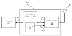
[0010]도 4는 도 2의 무선 디바이스 내에 포함된 트랜시버의 단순화된 블록도이다.
[0011]도 5는 도 2의 무선 디바이스 내에 포함된 트랜시버의 다른 실시예의 블록도이다.
[0012]도 6a는 일부 실시예들에 따른, 정정 모듈의 블록도이다.
[0013]도 6b는 도 6a의 정정 서브-모듈의 다른 실시예의 블록도이다.
[0014]도 7은 일부 실시예들에 따른, 도 5의 믹서 유닛의 블록도이다.
[0015]도 8a는 일부 실시예들에 따른, 정정 모듈 제어기의 블록도이다.
[0016]도 8b는 도 5의 트랜시버에 대한 예시적인 동작 모드들을 도시하는 예시적인 테이블이다.
[0017]도 9는 도 2의 무선 디바이스의 다른 예시적인 실시예인 디바이스를 도시한다.
[0018]도 10은 일부 실시예들에 따른, 도 1의 무선 디바이스에 대한 예시적인 동작을 도시하는 예시적인 흐름도를 도시한다.[0006] The embodiments are shown by way of example and are not intended to be limited by the figures of the accompanying drawings. Like reference numerals refer to like elements throughout the drawings and the specification.
[0007] Figure 1 illustrates a wireless device in communication with a wireless communication system, in accordance with some example embodiments.
[0008] FIG. 2 illustrates an exemplary design of the receiver and transmitter of FIG.
[0009] FIG. 3 is a band diagram illustrating three exemplary band groups that may be supported by the wireless device of FIG. 1;
[0010] FIG. 4 is a simplified block diagram of a transceiver included in the wireless device of FIG. 2.
[0011] FIG. 5 is a block diagram of another embodiment of a transceiver included in the wireless device of FIG. 2.
[0012] FIG. 6A is a block diagram of a correction module, in accordance with some embodiments.
[0013] FIG. 6B is a block diagram of another embodiment of the correction sub-module of FIG. 6A.
[0014] FIG. 7 is a block diagram of the mixer unit of FIG. 5, in accordance with some embodiments.
[0015] Figure 8A is a block diagram of a correction module controller, in accordance with some embodiments.
[0016] FIG. 8B is an exemplary table illustrating exemplary operational modes for the transceiver of FIG. 5.
[0017] FIG. 9 illustrates a device that is another exemplary embodiment of the wireless device of FIG. 2.
[0018] FIG. 10 illustrates an exemplary flow diagram illustrating exemplary operation for the wireless device of FIG. 1, in accordance with some embodiments.
[0019]다음의 설명에서, 본 개시내용의 철저한 이해를 제공하기 위해 특정 컴포넌트들, 회로들, 및 프로세스들의 예들과 같은 다수의 특정 세부사항들이 제시된다. 본원에 사용된 용어 "커플링되는"은 직접 커플링되거나 또는 하나 또는 그 초과의 개재된 컴포넌트들 또는 회로들를 통해 커플링되는 것을 의미한다. 또한, 다음의 상세한 설명에서 그리고 설명의 목적으로, 본 실시예들의 완전한 이해를 제공하기 위해 구체적인 명명법 및/또는 세부사항들이 제시된다. 그러나, 이들 특정 세부사항들이 본 실시예들을 실시하기 위해 필요로 되지 않을 수 있다는 것은 당업자에게 명백할 것이다. 다른 예시들에서, 본 개시내용을 불명료하게 하는 것을 회피하기 위해서, 잘 알려진 회로들 및 디바이스들은 블록도 형태로 도시되어 있다. 본원에 설명된 다양한 버스들을 통해 제공된 신호들 중 임의의 신호는 다른 신호들과 시간-멀티플렉싱될 수 있고 하나 또는 그 초과의 공통 버스들을 통해 제공될 수 있다. 추가로, 회로 엘리먼트들 또는 소프트웨어 블록들 간의 상호접속이 버스들 또는 단일 신호 라인들로 도시될 수 있다. 버스들 각각은 대안으로 단일 신호 라인일 수 있고, 단일 신호 라인들의 각각은 대안으로 버스들일 수 있고, 단일 라인 또는 버스는 컴포넌트들 간의 통신을 위한 무수한 물리적 또는 논리적 메카니즘들 중 임의의 하나 또는 그 초과의 것을 나타낼 수 있다. 본 실시예들이, 본원에 설명된 특정 예들로 제한된다기 보다는, 첨부된 청구항들에 의해 정의된 모든 컴포넌트들을 본 실시예들의 범위 내에서 포함하는 것으로 해석되어야 한다.[0019] In the following description, numerous specific details are set forth such as examples of specific components, circuits, and processes in order to provide a thorough understanding of the present disclosure. As used herein, the term "coupled" means coupled directly or coupled through one or more intervening components or circuits. In the following detailed description and for the purposes of explanation, specific nomenclature and / or details are set forth in order to provide a thorough understanding of the embodiments. However, it will be apparent to those skilled in the art that these specific details may not be required to practice these embodiments. In other instances, well known circuits and devices are shown in block diagram form in order to avoid obscuring the present disclosure. Any of the signals provided over the various busses described herein may be time-multiplexed with other signals and provided over one or more common busses. Additionally, interconnection between circuit elements or software blocks may be illustrated as buses or single signal lines. Each of the buses may alternatively be a single signal line, each of the single signal lines may alternatively be a bus, and a single line or bus may be any one or more of any of a myriad of physical or logical mechanisms for communication between the components Can be represented. It should be understood that these embodiments are not limited to the specific examples described herein but rather include all of the components defined by the appended claims within the scope of the embodiments.
[0020]이외에도, 첨부된 도면들과 관련하여 아래에 제시되는 상세한 설명은, 본 개시내용의 예시적인 실시예들의 설명으로서 의도되며, 본 개시내용이 실시될 수 있는 유일한 실시예들만을 나타내도록 의도되지 않는다. 본 설명 전반에 걸쳐 사용되는 용어 "예시적인"은 "예, 예시, 또는 예증으로서 기능하는 것"을 의미하고, 다른 실시예들에 비해 반드시 바람직하거나 유리한 것으로서 해석되지는 않아야 한다.[0020] In addition, the following detailed description, taken in conjunction with the accompanying drawings, is intended as a description of exemplary embodiments of the present disclosure, and is intended to show only those embodiments in which the present disclosure may be practiced It does not. The word "exemplary " used throughout this description means" serving as an example, instance, or illustration, " and should not necessarily be construed as preferred or advantageous over other embodiments.
[0021]도 1은 일부 예시적인 실시예들에 따른, 무선 통신 시스템(120)과 통신하는 무선 디바이스(110)를 도시한다. 무선 통신 시스템(120)은, LTE(Long Term Evolution) 시스템, CDMA(Code Division Multiple Access) 시스템, GSM(Global System for Mobile Communications) 시스템, WLAN(wireless local area network) 시스템 또는 몇몇 다른 무선 시스템일 수 있다. CDMA 시스템은 광대역 WCDMA(Wideband CDMA), CDMA 1X, EVDO(Evolution-Data Optimized), TD-SCDMA(Time Division Synchronous CDMA), 또는 CDMA의 일부 다른 버전들을 구현할 수 있다. 간결함을 위해, 도 1은 2개의 기지국들(130 및 132) 및 하나 시스템 제어기(140)를 포함하는 무선 통신 시스템(120)을 도시한다. 일반적으로, 무선 시스템은 임의의 수의 기지국들 및 임의의 세트의 네트워크 엔티티들을 포함할 수 있다.[0021] FIG. 1 illustrates a
[0022]무선 디바이스(110)는 또한, 사용자 장비(UE), 모바일 스테이션, 단말, 액세스 단말, 가입자 유닛, 스테이션 등으로 지칭될 수 있다. 무선 디바이스(110)는 셀룰러 폰, 스마트 폰, 태블릿, 무선 모뎀, PDA(personal digital assistant), 핸드 헬드 디바이스, 랩탑 컴퓨터, 스마트북, 넷북, 무선 전화기, WLL(wireless local loop) 스테이션, 블루투스 디바이스 등일 수 있다. 무선 디바이스(110)는 무선 통신 시스템(120)과 통신할 수 있다. 무선 디바이스(110)는 또한, 하나 또는 그 초과의 GNSS(global navigation satellite system) 등에서, 브로드캐스트 스테이션들(예를 들어, 브로드캐스트 스테이션(134))로부터의 신호들, 위성들(예를 들어, 위성(150))로부터의 신호들을 수신할 수 있다. 무선 디바이스(110)는, LTE, WCDMA, CDMA 1X, EVDO, TD-SCDMA, GSM, 802.11 등과 같은 무선 통신을 위한 하나 또는 그 초과의 라디오 기술들을 지원할 수 있다.[0022] The
[0023]도 2는 도 1의 무선 디바이스(110)의 예시적인 설계의 블록도를 도시한다. 본 예시적인 설계에서, 무선 디바이스(110)는 1차 안테나(210)에 커플링된 1차 트랜시버(220), 2차 안테나(212)에 커플링된 2차 트랜시버(222), 및 데이터 프로세서/제어기(280)를 포함한다. 1차 트랜시버(220)는 다수의 주파수 대역들, 다수의 라디오 기술들, 반송파 집성 등을 지원하기 위해서 다수(K)개의 수신기들(230pa 내지 230pk) 및 다수(K)개의 송신기들(250pa 내지 250pk)을 포함한다. 2차 트랜시버(222)는, 다수의 주파수 대역들, 다수의 라디오 기술들, 반송파 집성, 수신 다이버시티, 다수의 송신 안테나들로부터 다수의 수신 안테나들로의 MIMO(multiple-input multiple-output) 송신 등을 지원하기 위해, 다수(L)개의 수신기들(230sa 내지 230sl) 및 다수(L)개의 송신기들(250sa 내지 250sl)을 포함한다.[0023] FIG. 2 shows a block diagram of an exemplary design of the
[0024]도 2에 도시된 예시적인 설계에서, 각각의 수신기(230)(예를 들어, 230pa 내지 230pk 및 230sa 내지 230sl)는 LNA(low noise amplifier)(240)(예를 들어, 240pa 내지 240pk 및 240sa 내지 240sl) 및 수신 회로들(242)(예를 들어, 242pa 내지 242pk 및 242sa 내지 242sl)을 포함한다. 데이터 수신의 경우, 1차 안테나(210)는, 기지국들 및/또는 다른 송신기 스테이션들로부터 신호들을 수신하고 수신된 RF(radio frequency) 신호를 제공하며, 이 수신된 RF 신호는, 안테나 인터페이스 회로(224)를 통해 라우팅되고 입력 RF 신호로서 선택된 수신기에 제공된다. 안테나 인터페이스 회로(224)는 스위치들, 듀플렉서들, 송신 필터들, 수신 필터들, 매칭 회로들 등을 포함할 수 있다. 아래의 설명은, 수신기(230pa)가 선택된 수신기라고 가정한다. 수신기(230pa)에서, LNA(240pa)는 입력 RF 신호를 증폭시키고 출력 RF 신호를 제공한다. 수신 회로들(242pa)은 출력 RF 신호를 RF로부터 기저대역으로 하향변환하고, 하향변환된 신호를 증폭 및 필터링하고, 그리고 아날로그 입력 신호를 데이터 프로세서/제어기(280)로 제공한다. 수신 회로들(242pa)은 믹서들, 필터들, 증폭기들, 매칭 회로들, 발진기, LO(local oscillator) 발생기, PLL(phase locked loop) 등을 포함할 수 있다. 트랜시버들(220 및 222) 내 각각의 나머지 수신기(230)는 수신기(230pa)와 유사한 방식으로 동작할 수 있다.[0024] In the exemplary design shown in FIG. 2, each receiver 230 (e.g., 230pa to 230pk and 230sa to 230sl) includes a low noise amplifier (LNA) 240 (e.g., 240pa to 240pk And 240sa through 240sl and receive circuits 242 (e.g., 242pA through 242pk and 242sa through 242sl). In the case of data reception, the
[0025]도 2에 도시된 예시적인 설계에서, 각각의 송신기(250)(예를 들어, 250pa 내지 250pk 및 250sa 내지 250sl)는 송신 회로들(252)(예를 들어, 252pa 내지 252pk 및 252sa 내지 252sl) 및 PA(power amplifier)(254)(예를 들어, 254pa 내지 254pk 내지 254sa 내지 254sl)를 포함한다. 데이터 송신의 경우, 데이터 프로세서/제어기(280)는 송신될 데이터를 프로세싱(예를 들어, 인코딩 및 변조)하고 아날로그 출력 신호를 선택된 송신기에 제공한다. 아래의 설명은, 송신기(250pa)가 선택된 송신기라는 것을 가정한다. 송신기(250pa)에서, 송신 회로들(252pa)은 아날로그 출력 신호를 증폭, 필터링하고, 기저대역으로부터 RF로 상향변환하여, 변조된 RF 신호를 제공한다. 송신 회로들(252pa)은, 증폭기들, 필터들, 믹서들, 매칭 회로들, 발진기, LO 생성기, PLL 등을 포함할 수 있다. PA(254pa)는 변조된 RF 신호를 수신하고 증폭하며 적절한 출력 전력 레벨을 갖는 송신 RF 신호를 제공한다. 송신 RF 신호는 안테나 인터페이스 회로(224)를 통해 라우팅되고 1차 안테나(210)를 통해 송신된다. 트랜시버들(220 및 222) 내 각각의 나머지 송신기(250)는 송신기(250pa)와 유사한 방식으로 동작할 수 있다. 예를 들어, 제 2 RF 신호가 안테나 인터페이스 회로(226)를 통해 라우팅되고, 2차 안테나(212)를 통해 송신 및/또는 수신될 수 있다.[0025] In the exemplary design shown in FIG. 2, each transmitter 250 (e.g., 250pA to 250pk and 250sa to 250sl) includes transmit circuits 252 (e.g., 252pA to 252pk, 252sl) and a power amplifier (PA) 254 (e.g., 254pA to 254pk to 254sa to 254sl). In the case of data transmission, the data processor /
[0026]각각의 수신기(230) 및 송신기(250)는 또한 도 2에 도시되지 않은 다른 회로들, 이를 테면, 필터들, 매칭 회로들 등을 포함할 수 있다. 트랜시버들(220 및 222)의 전부 또는 일부가 하나 또는 그 초과의 아날로그 IC(integrated circuit)들, RF IC들(RFIC들), 혼합-신호 IC들 등 상에서 구현될 수 있다. 예를 들어, 트랜시버들(220 및 222) 내의 LNA들(240) 및 수신 회로들(242)은, 아래에 설명되는 바와 같이 다수의 IC 칩들 상에서 구현될 수 있다. 트랜시버들(220 및 222)의 회로들은 또한 다른 방식들로 구현될 수 있다.[0026] Each receiver 230 and transmitter 250 may also include other circuits not shown in FIG. 2, such as filters, matching circuits, and the like. All or a portion of the
[0027]데이터 프로세서/제어기(280)는 무선 디바이스(110)를 위한 다양한 기능들을 수행할 수 있다. 예를 들어, 데이터 프로세서/제어기(280)는 수신기들(230)을 통해 수신되는 데이터 및 송신기들(250)을 통해 송신되는 데이터에 대한 프로세싱을 수행할 수 있다. 데이터 프로세서/제어기(280)는 트랜시버들(220 및 222) 내의 다양한 회로들의 동작을 제어할 수 있다. 메모리(282)는 데이터 프로세서/제어기(280)를 위한 프로그램 코드들 및 데이터를 저장할 수 있다. 데이터 프로세서/제어기(280)는 하나 또는 그 초과의 ASIC(application specific integrated circuit)들 및/또는 다른 IC들 상에서 구현될 수 있다.[0027] Data processor /
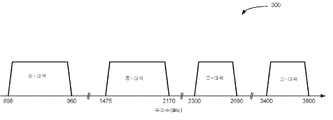
[0028]도 3은 무선 디바이스(110)에 의해 지원될 수 있는 3개의 예시적인 대역 그룹들을 도시하는 대역 다이어그램(300)이다. 일부 실시예들에서, 무선 디바이스(110)는 1000 MHz(megahertz) 보다 낮은 주파수들을 갖는 RF 신호들을 포함하는 저-대역(LB), 1000 MHz 내지 2300 MHz의 주파수들을 갖는 RF 신호들을 포함하는 중-대역(MB), 및/또는 2300 MHz 보다 높은 주파수들을 갖는 RF 신호들을 포함하는 고-대역(HB)에서 동작할 수 있다. 예를 들어, 도 3에 도시된 바와 같이, 저-대역 RF 신호들은 698 MHz 내지 960 MHz를 커버할 수 있고, 중-대역 RF 신호들은 1475 MHz 내지 2170 MHz를 커버할 수 있고, 고-대역 RF 신호들은 2300 MHz 내지 2690 MHz, 및 3400 MHz 내지 3800 MHz를 커버할 수 있다. 저-대역, 중-대역 및 고-대역은 대역들의 3개의 그룹들(또는 대역 그룹들)을 지칭하며, 각각의 대역 그룹은 다수의 주파수 대역들(또는 단순히 "대역들")을 포함한다. 각각의 대역은 200 MHz까지 커버할 수 있다. LTE 릴리즈 11은, LTE/UMTS 대역들로서 지칭되고 3GPP TS 36.101에서 나열되는 35개의 대역들을 지원한다.[0028] FIG. 3 is a band diagram 300 illustrating three exemplary band groups that may be supported by the
[0029]일반적으로, 임의의 수의 대역 그룹들이 정의될 수 있다. 각각의 대역 그룹은 도 3에 도시된 주파수 범위들 중 임의의 것과 매칭되거나 매칭되지 않을 수 있는 주파수들의 임의의 범위를 커버할 수 있다. 각각의 대역 그룹은 또한 임의의 수의 대역들을 포함할 수 있다.[0029] In general, any number of band groups may be defined. Each band group may cover any range of frequencies that may or may not match any of the frequency ranges shown in FIG. Each band group may also include any number of bands.
[0030]도 4는 도 2의 무선 디바이스(110) 내에 포함될 수 있는 트랜시버(400)의 단순화된 블록도이다. 예를 들어, 트랜시버(400)는 1차 트랜시버(220) 또는 2차 트랜시버(222)일 수 있다. 트랜시버(400)는 디지털 통신 신호들(415)을 디지털 모뎀(410)과 교환할 수 있다. 일부 실시예들에서, 디지털 모뎀(410)은 데이터 프로세서/제어기(280) 내에 포함될 수 있다. 디지털 모뎀(410)은 디지털 통신 신호들을 트랜시버(400)로 제공할 수 있고, 그리고/또는 트랜시버(400)로부터 디지털 통신 신호들을 수신할 수 있다.[0030] FIG. 4 is a simplified block diagram of a
[0031]트랜시버(400)는 디지털 기저대역 프로세싱 유닛(420) 및 아날로그 프로세싱 유닛(430)을 포함할 수 있다. 일부 실시예들에서, 디지털 기저대역 프로세싱 유닛(420)은 디지털 통신 신호들(415)(예를 들어, 디지털 송신 및/또는 수신 통신 신호들)을 아날로그 통신 신호들(453)(예를 들어, 아날로그 송신 및/또는 수신 통신 신호들)로 변환할 수 있다. 예를 들어, 디지털 송신 통신 신호가 디지털 기저대역 프로세싱 유닛(420)에 의해 디지털 모뎀(410)으로부터 수신될 수 있다. 디지털 송신 통신 신호는, 아날로그 송신 통신 신호를 생성하기 위해 디지털 기저대역 프로세싱 유닛(420) 내에 포함되는 디지털-투-아날로그 컨버터(간결함을 위해 미도시)에 의해 프로세싱될 수 있다. 아날로그 프로세싱 유닛(430)이 아날로그 송신 통신 신호를 수신하고, 상향변환한 후, 안테나(440)를 통해 상향변환된 신호를 송신할 수 있다. 유사한 방식으로, 통신 신호가 안테나(440)에 의해 수신되고, 아날로그 프로세싱 유닛(430)에 의해 아날로그 수신 통신 신호로 하향변환되고, 그리고 디지털 기저대역 프로세싱 유닛(420) 내에 포함되는 아날로그-투-디지털 컨버터(간결함을 위해 미도시)을 통해 디지털 수신 통신 신호로 변환될 수 있다.[0031] The
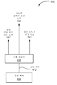
[0032]일부 실시예들에서, 디지털 기저대역 프로세싱 유닛(420)은, 정정 신호(452)를 생성하는 정정 모듈(450)을 포함할 수 있다. 정정 신호(452)는 아날로그 송신 통신 신호와 연관된 하나 또는 그 초과의 손상들을 정정하기 위해 사용될 수 있다. 예를 들어, 정정 신호(452)는 아날로그 송신 통신 신호와 연관된 상호 변조 왜곡의 전부 또는 일부를 상쇄하고, 아날로그 송신 통신 신호를 등화하고, 그리고/또는 아날로그 송신 통신 신호를 사전 왜곡시킬 수 있다. 일부 실시예들에서, 정정 신호(452)가 아날로그 프로세싱 유닛(430) 내에서 아날로그 송신 통신 신호와 결합될 수 있다. 정정 모듈(450)의 동작 및 정정 신호(452)의 생성이 아래의 도 5 내지 도 7과 관련하여 보다 상세하게 설명된다.[0032] In some embodiments, the digital
[0033]도 5는 도 2의 무선 디바이스(110) 내에 포함될 수 있는 트랜시버(500)의 다른 실시예의 블록도이다. 트랜시버(500)는 디지털 기저대역 프로세싱 유닛(520) 및 아날로그 프로세싱 유닛(530)을 포함할 수 있다. 트랜시버(400)와 유사하게, 디지털 기저대역 프로세싱 유닛(520)은 디지털 모뎀(410)(간결함을 위해 미도시)으로부터의 디지털 통신 신호들(예를 들어, 디지털 기저대역 신호들)을 아날로그 프로세싱 유닛(530)을 위해 아날로그 통신 신호들(예를 들어, 아날로그 기저대역 신호들)로 변환할 수 있다. 또한, 디지털 기저대역 프로세싱 유닛(520)은 아날로그 프로세싱 유닛(530)으로부터의 아날로그 통신 신호들을 디지털 모뎀(410)을 위해 디지털 통신 신호들로 변환할 수 있다.[0033] FIG. 5 is a block diagram of another embodiment of a
[0034]디지털 기저대역 프로세싱 유닛(520)은 DAC(digital-to-analog converter)/ADC(analog-to-digital converter) 유닛(521), DAC/ADC 유닛(522), 정정 모듈(560), 및 피드백 수신기(525)를 포함할 수 있다. DAC/ADC 유닛(521)은 디지털 모뎀(410)(간결함을 위해 도 5에 미도시)으로부터 제 1 송신기와 연관된 디지털 송신 통신 신호(571)를 수신할 수 있다. DAC/ADC 유닛(521)은 디지털 송신 통신 신호(571)를 아날로그 송신 통신 신호(573)로 변환할 수 있다. 또한, DAC/ADC 유닛(521)은 제 1 수신기와 연관된 아날로그 수신 통신 신호(574)를 수신할 수 있고, 이에 대한 응답으로, 디지털 수신 통신 신호(572)를 생성할 수 있다. 일부 실시예에서, 트랜시버(500)는 2개 또는 그 초과의 송신기/수신기 쌍들을 지원할 수 있다. 따라서, DAC/ADC 유닛(522)은 디지털 모뎀(410)으로부터 제 2 송신기와 연관된 디지털 송신 통신 신호(575)를 수신할 수 있고, 이에 대한 응답으로, 아날로그 프로세싱 유닛(530)을 위해 아날로그 송신 통신 신호(577)를 생성할 수 있다. DAC/ADC 유닛(522)은 또한, 제 2 수신기와 연관된 아날로그 수신 통신 신호(578)를 수신할 수 있고, 이에 대한 응답으로, 디지털 수신 통신 신호(576)를 생성할 수 있다. 당업자는, 디지털 기저대역 프로세싱 유닛(520) 및 아날로그 프로세싱 유닛(530)이 직교 위상 및/또는 차동 신호들을 프로세싱할 수 있다는 것을 인식할 것이다. 예를 들어, 디지털 송신 통신 신호(571)는 2개의 신호들: 디지털 동위상 신호 및 디지털 직교 위상 신호를 포함할 수 있다. 또한, 일부 실시예들에서, 디지털 동위상 신호 및 디지털 직교 위상 신호는 차동 신호들일 수 있다.The digital baseband processing unit 520 includes a digital-to-analog converter (DAC) / analog-to-digital converter (ADC)
[0035]아날로그 프로세싱 유닛(530)은 제 1 믹서 유닛(540), 제 2 믹서 유닛(545), 출력 선택기(550), 피드백 신호 선택기(551), 증폭기(552 - 555), 제 1 커플러(556), 및 제 2 커플러(557)를 포함할 수 있다. 아날로그 통신 신호들은 디지털 기저대역 프로세싱 유닛(520)과 아날로그 프로세싱 유닛(530) 사이에서 교환될 수 있다. 따라서, 제 1 송신기/수신기 쌍과 연관된 아날로그 통신 신호들(예를 들어, 아날로그 송신 통신 신호(573) 및 아날로그 수신 통신 신호(574))이 믹서 유닛(540)과 DAC/ADC 유닛(521) 사이에 커플링될 수 있다. 유사한 방식으로, 제 2 송신기/수신기 쌍과 연관된 아날로그 통신 신호들(예를 들어, 아날로그 송신 통신 신호(577) 및 아날로그 수신 통신 신호(578))이 믹서 유닛(545)과 DAC/ADC 유닛(522) 사이에 커플링될 수 있다.The analog processing unit 530 includes a
[0036]일부 실시예들에서, 믹서 유닛(540)이 국부 발진기 신호(간결함을 위해 도 5에 미도시)에 기초하여 아날로그 송신 통신 신호(573)를 상향변환하고, 변조된 송신 통신 신호(580)를 생성할 수 있다. 믹서 유닛(540)은 또한, 변조된 수신 통신 신호(581)를 하향변환하고, 아날로그 수신 통신 신호(574)를 생성할 수 있다. 일부 실시예들에서, 변조된 송신 통신 신호(580)가 증폭기(553)에 의해 버퍼링될 수 있고, 수신된 변조된 통신 신호(582)는 증폭기(552)에 의해 버퍼링될 수 있다. 유사한 방식으로, 믹서 유닛(545)은 아날로그 송신 통신 신호(577)를 상향변환하고, 변조된 송신 통신 신호(583)를 생성할 수 있다. 믹서 유닛(545)은 또한, 변조된 수신 통신 신호(584)를 하향변환하고, 아날로그 수신 통신 신호(578)를 생성할 수 있다. 일부 실시예들에서, 변조된 송신 통신 신호(583)가 증폭기(555)에 의해 버퍼링될 수 있고, 수신된 변조된 통신 신호(585)는 증폭기(554)에 의해 버퍼링될 수 있다.In some embodiments, the
[0037]정정 모듈(560)은 변조된 송신 통신 신호와 연관될 수 있는 하나 또는 그 초과의 손상들을 정정하는 정정 신호(586)를 생성할 수 있다. 일부 실시예에서, 정정 모듈(560)은 도 4에 설명된 정정 모듈(450)의 다른 실시예일 수 있다. 유사한 방식으로, 정정 신호(586)는 도 4의 정정 신호(452)의 다른 실시예일 수 있다. 일 실시예에서, 정정 신호(586)는 다른 송신 통신 신호에 의해 야기된 상호 변조 왜곡을 정정할 수 있다. 예를 들어, 제 1 송신기 및 제 2 송신기 둘 모두가 동시에 또는 거의 동시에 동작할 경우, 제 1 송신기는 제 2 송신기에서 왜곡(이를 테면, 상호 변조 왜곡)을 유도할 수 있다. 정정 모듈(560)은, 제 2 송신기에서의 상호 변조 왜곡을 중화시키는(counteract)(또는 감소시키는) 정정 신호(586)를 생성할 수 있다. 다른 실시예에서, 정정 신호(586)는 송신 통신 신호와 연관된 하나 또는 그 초과의 비선형성들을 정정하거나 또는 중화시킬 수 있다. 예를 들어, 정정 신호(586)는 송신 통신 신호를 사전 왜곡시키거나 또는 등화시킬 수 있다.[0037]
[0038]정정 모듈(560)은 디지털 송신 통신 신호(571), 디지털 수신 통신 신호(572), 디지털 송신 통신 신호(575), 디지털 수신 통신 신호(576), 디지털 피드백 신호(589), 및/또는 정정 모듈 모드 제어 신호(587)에 기초하여 정정 신호(586)를 생성할 수 있다. 일부 실시예들에서, 피드백 수신기(525)는 변조된 송신 통신 신호를 수신 및 복조하고, 복조된 송신 통신 신호에 기초하여 디지털 피드백 신호(589)를 생성하고, 디지털 피드백 신호(589)를 정정 모듈(560)에 제공할 수 있다. 피드백 수신기(525)는 피드백 신호 선택기(551)에 커플링될 수 있다. 피드백 신호 선택기(551)는 피드백 선택기 제어 신호(590)에 기초하여 제 1 송신기 또는 제 2 송신기와 연관된 변조된 송신 통신 신호를 선택할 수 있다. 일부 실시예들에서, 변조된 아날로그 송신 신호가 증폭기(553) 및/또는 증폭기(555)에 의해 제공될 수 있다. 커플러(556)는 제 1 송신기와 연관된 변조된 아날로그 송신 신호를 피드백 신호 선택기(551)에 제공할 수 있다. 유사한 방식으로, 커플러(557)는 제 2 송신기와 연관된 변조된 아날로그 송신 신호를 피드백 신호 선택기(551)에 제공할 수 있다. 일부 실시예들에서, 커플러(556) 및 커플러(557)는 방향성 커플러일 수 있다. 정정 모듈(560) 및 피드백 신호 선택기(551)의 동작은 도 6 및 도 8과 관련하여 아래에 보다 상세하게 설명된다.The
[0039]정정 신호(586)는 각각, 믹서 유닛(540) 및 믹서 유닛(545) 내부에서 아날로그 송신 통신 신호(573)와 연관된 변조된 송신 통신 신호 또는 아날로그 송신 통신 신호(577)와 연관된 변조된 송신 통신 신호에 가산될 수 있다. 일부 실시예들에서, 정정 신호(586)는 하나 또는 그 초과의 DAC들(간결함을 위해 미도시)을 통해 디지털 신호로부터 아날로그 신호로 변환될 수 있다. 믹서 유닛(540) 및 믹서 유닛(545)의 동작들이 도 7과 관련하여 아래에 보다 상세하게 설명된다. 일부 실시예들에서, 정정 신호(586)는 출력 선택기(550)를 통해 믹서 유닛(540) 또는 믹서 유닛(545)으로 라우팅될 수 있다. 출력 선택기(550)는 출력 선택기 제어 신호(591)에 의해 제어될 수 있다. 출력 선택기(550)의 동작들이 도 8과 관련하여 아래에 보다 상세하게 설명된다.
[0040]도 6a는 일부 실시예들에 따른, 정정 모듈(560)의 블록도이다. 정정 모듈(560)은 입력 선택기(602), 분석 유닛(601), 제 1 정정 서브-모듈(603), 제 2 정정 서브-모듈(604), 및 합산 노드(620)를 포함할 수 있다. 제 1 정정 서브-모듈(603) 및 제 2 정정 서브-모듈(604)만이 도시되었지만, 정정 모듈(560)의 다른 실시예들은 다른 개수의 정정 서브-모듈들(간결함을 위해 미도시)을 포함할 수 있다. 예를 들어, 정정 모듈(560)의 일부 실시예들은 다수(N)개의 정정 서브-모듈들을 포함할 수 있다.[0040] FIG. 6A is a block diagram of a
[0041]각각의 정정 서브-모듈은 위상 수정 유닛, 지연 수정 유닛, 및 증폭 수정 유닛을 포함할 수 있다. 예를 들어, 제 1 정정 서브-모듈(603)은 지연 수정 유닛(610), 위상 수정 유닛(611), 및 진폭 수정 유닛(612)을 포함할 수 있다. 유사한 방식으로, 제 2 정정 서브-모듈(604)은 지연 수정 유닛(615), 위상 수정 유닛(616), 및 진폭 수정 유닛(617)을 포함할 수 있다. 정정 서브-유닛들의 다른 실시예들은 3개 미만의 수정 유닛들, 가산 유닛들 및/또는 복제(예를 들어, 리던던트) 유닛들을 포함할 수 있다.[0041] Each of the correction sub-modules may include a phase correction unit, a delay correction unit, and an amplification correction unit. For example, the
[0042]디지털 통신 신호는 입력 선택기(602)에 의해 제 1 정정 서브-모듈(603) 및/또는 제 2 정정 서브- 모듈(604)에 제공될 수 있다. 입력 선택기(602)는 디지털 송신 통신 신호(571), 디지털 수신 통신 신호(572), 디지털 송신 통신 신호(575), 디지털 수신 통신 신호(576), 및 디지털 피드백 신호(589)를 수신할 수 있다. 일 실시예에서, 제 1 정정 서브-모듈(603) 및/또는 제 2 정정 서브-모듈(604)은, 선택된 디지털 통신 신호의 타이밍(예를 들어, 지연), 위상, 및/또는 진폭을 수정할 수 있다. 예를 들어, 제 1 정정 서브-모듈(603)은, 지연 수정 유닛(610)을 통해 디지털 통신 신호를 지연시킴으로써 디지털 통신 신호의 지연을 조정할 수 있다. 또한, 위상 수정 유닛(611)은 디지털 통신 신호의 위상을 조정할 수 있고, 진폭 수정 유닛(612)은 디지털 통신 신호와 연관된 진폭을 증가 또는 감소시킬 수 있다. 유사한 방식으로, 디지털 통신 신호는 제 2 정정 서브-모듈(604)에 의해 수정될 수 있다. 도 6a에서 예시적인 순서로 도시되었지만, 다른 실시예들에서, 지연 수정 유닛들(610 및 615), 위상 수정 유닛들(611 및 616), 및 진폭 수정 유닛들(612 및 617)은 임의의 기술적으로 실행가능한 순서로 배열될 수 있다. 따라서, 지연, 위상 및 진폭 수정들은, 제 1 정정 서브-모듈(603) 및/또는 제 2 정정 서브-모듈(604)에서 임의의 기술적으로 실행가능한 순서로 발생할 수 있다.The digital communication signal may be provided to the
[0043]일부 실시예들에서, 위상, 지연 및 진폭 수정들은 복수의 필터 탭들을 갖는 디지털 필터들에 의해 달성될 수 있다. 예를 들어, 지연 수정 유닛(610), 위상 수정 유닛(611), 및/또는 진폭 수정 유닛(612)은, 디지털 신호의 위상, 지연, 및 진폭을 각각 수정하기 위한 디지털 필터(예를 들어, FIR(finite impulse response) 또는 IIR(infinite impulse response) 필터)를 각각 포함할 수 있다. 유사한 방식으로, 지연 수정 유닛(615), 위상 수정 유닛(616), 및 진폭 수정 유닛(617)은 각각 디지털 필터들을 포함할 수 있다.[0043] In some embodiments, phase, delay, and amplitude modifications may be achieved by digital filters having a plurality of filter taps. For example, the delay correction unit 610, the phase correction unit 611, and / or the
[0044]일부 실시예에서, 제 1 정정 서브-모듈(603) 및/또는 제 2 정정 서브-모듈(604) 내에 제공되는 위상 수정, 지연 수정 및/또는 진폭 수정의 양이 분석 유닛(601)에 의해 제공되는 서브-모듈 셋팅들에 의해 결정될 수 있다. 일부 실시예들에서, 서브-모듈 셋팅들은 연관된 정정 서브-모듈 내에서 하나 또는 그 초과의 필터 탭들을 구성할 수 있다. 예를 들어, 제 1 정정 서브-모듈(603)에 대한 서브-모듈 셋팅들은 지연 수정 유닛(610), 위상 수정 유닛(611), 및/또는 진폭 수정 유닛(612) 내에서 필터 탭들을 구성할 수 있다. 유사한 방식으로, 제 2 정정 서브-모듈(604)에 대한 서브-모듈 셋팅들은 지연 수정 유닛(615), 위상 수정 유닛(616), 및/또는 진폭 수정 유닛(617) 내에서 필터 탭들을 구성할 수 있다. 일부 실시예들에서, 각각의 정정 서브-모듈로부터의 출력 신호들은, 정정 신호(586)를 생성하기 위해 합산 노드(620)에서 함께 합산될 수 있다.[0044] In some embodiments, the amount of phase correction, delay correction, and / or amplitude correction provided in the
[0045]일 실시예에서, 정정 모듈(560)은 동작 모드에 기초하여 정정 신호(586)를 생성하도록 구성될 수 있다. 예를 들어, 일부 동작 모드들이, 상호 변조 왜곡을 감소시키거나 감쇠시키기 위한 정정 신호(586)를 생성할 수 있다. 상호 변조 왜곡은, 희생 신호(victim signal)를 간섭하는 공격 신호(aggressor signal)에 의해 야기될 수 있다. 예를 들어, 제 1 변조된 송신 통신 신호(공격 신호)가 제 2 변조된 송신 통신 신호(희생 신호)를 간섭할 수 있다. 다른 예에서, 제 2 변조된 송신 통신 신호(공격 신호)가 제 1 변조된 송신 통신 신호(희생 신호)를 간섭할 수 있다. 따라서, 일부 실시예들에서, 정정 신호(586)는, 공격 신호로부터 하나 또는 그 초과의 희생 신호들에 대한 간섭을 감소시키도록 구성될 수 있다.[0045] In one embodiment, the
[0046]제 1 동작 모드(예를 들어, 캘리브레이션 모드)에서, 제 1 정정 서브-모듈(603) 및/또는 제 2 정정 서브-모듈(604)에 대한 최초 서브-모듈 셋팅들은, 상호 변조 왜곡을 감소시키거나 감쇠시키도록 분석 유닛(601)에 의해 결정될 수 있다. 희생 신호는 변조된 송신 통신 신호(580)일 수 있고, 공격 신호는 변조된 송신 통신 신호(583)일 수 있다(도 5를 또한 참조한다). 최초 서브-모듈 셋팅들은 분석 유닛(601)에서 수신된 공격 신호에 기초할 수 있다. 따라서, 입력 선택기(602)는 디지털 송신 통신 신호(575)를 제 1 정정 서브-모듈(603) 및 제 2 정정 서브-모듈(604)에 제공할 수 있고, 디지털 피드백 신호(589)를 분석 유닛(601)에 제공할 수 있다. 일부 실시예들에서, 디지털 피드백 신호(589)는 희생 신호(예를 들어, 변조된 송신 통신 신호(580))와 연관될 수 있다.[0046] In a first mode of operation (e.g., a calibration mode), the initial sub-module settings for the
[0047]일부 실시예들에서, 초기화 동안, 수신 신호 r(t)는 아래의 식 1로 표현될 수 있다:[0047] In some embodiments, during initialization, the received signal r (t) may be expressed by
![]()
![]()
여기서, h(t)는 누설 경로들을 기술하는 함수이고;Where h (t) is a function describing the leakage paths;
x(t)는 공격 신호를 기술하는 함수이고; 그리고x (t) is a function describing the attack signal; And
g(t)는 상쇄 신호를 기술하는 함수이다.g (t) is a function describing the cancellation signal.
[0048]따라서, 식 1은, 초기화 기간(예를 들어, 희생 송신기가 송신 중이지 않을 경우) 동안 수신 신호가 2개의 컴포넌트들: 누설 경로들(예를 들어, 상호 변조)로 인한 제 1 컴포넌트 및 상쇄 신호 g(t)로 인한 제 2 컴포넌트를 포함할 수 있다는 것을 표현한다. 누설 경로들로 인한 제 1 컴포넌트를 결정하기 위해서, 상쇄 신호 g(t) 컴포넌트는 식 (2)에 나타내어진 바와 같이 제로로 셋팅될 수 있다.[0048] Thus,
![]()
![]()
[0049]다음으로, 수신 신호는, 아래의 식 3을 산출하는 분석 유닛(601)에 의해 기록될 수 있다 (예를 들어, 수신 신호의 다수(M)개의 샘플들이 기록될 수 있다):Next, the received signal can be recorded by an
![]()
![]()
[0050]따라서, 상쇄 신호 g(t)가 공격 신호로부터의 영향들을 제거하는 경우는 다음 식과 같다:Therefore, when the cancel signal g (t) removes the influence from the attack signal, the following equation is obtained:
![]()
![]()
[0051]수신 신호 r(t)는 상술된 레코딩과 연관되는 이산적인 수의 샘플들(M)을 포함할 수 있기 때문에, r(t)는, 아래의 식 5에 나타내어진 바와 같이 벡터로 표현될 수 있다:Since the received signal r (t) may include a discrete number of samples M associated with the above-described recording, r (t) may be expressed as a vector as shown in Equation 5 below. Can be:
![]()
![]()
[0052]따라서, 상쇄 신호 g(t)에 대한 해(solving)가 아래의 식 6에서 나타내어진다 :[0052] Thus, the solving for the offset signal g (t) is shown in Equation 6 below:
![]()
![]()
X+는 X의 의사 역수이다![]()
![]()
[0053]이러한 방식으로, 상쇄 신호 g(t)의 최초 값이 결정될 수 있다. 예를 들어, 희생 신호와 연관된 송신기가 온 상태에 있지만, 데이터를 송신하고 있지 않는 동안, 수신 신호(디지털 피드백 신호(589))가 분석 유닛(601)에 의해 레코딩될 수 있다. 그런 다음, 분석 유닛(601)은 상쇄 신호 g(t)를 결정할 수 있고, 또한, 공격 신호에 기초하여 g(t)를 생성하는 방법을 결정할 수 있다. 다른 실시예들에서, 상쇄 신호 g(t)를 결정하기 위해 반복되는 샘플링 및 추정들이 사용될 수 있다. 예를 들어, 상쇄 신호 g(t)를 결정하기 위해 LMS(least-mean-square) 및/또는 RLS(recursive-least-squares) 연산들이 사용될 수 있다. 또 다른 실시예들에서, LMS, RLS 및/또는 식 6의 결합이 사용될 수 있다.In this way, the initial value of the offset signal g (t) can be determined. For example, a received signal (digital feedback signal 589) may be recorded by the
[0054]따라서, 분석 유닛(601)은 (예를 들어, 식 (6)을 사용하여) 상쇄 신호 g(t)를 생성하기 위해 서브-모듈 셋팅들을 결정할 수 있다. 일부 실시예들에서, 상쇄 신호 g(t)는 정정 서브-모듈(603) 및/또는 정정 서브-모듈(604) 내의 디지털 필터(예를 들어, FIR 또는 IIR 필터들)에 대한 탭 값들을 기술하고 그리고/또는 그 탭 값들과 연관될 수 있다. 일부 실시예들에서, 2개 이상의 정정 서브-모듈이 상쇄 신호 g(t)를 생성하기 위해 사용될 수 있다. 따라서, 분석 유닛(601)은 상쇄 신호 g(t)(예를 들어, 정정 신호(586))를 생성하기 위해 복수의 정정 서브-모듈들에 대한 서브-모듈 셋팅들을 결정할 수 있다. 제 1 정정 서브-모듈(603) 및/또는 제 2 정정 서브-모듈(604)은 디지털 송신 통신 신호(575)를 수정하고 정정 신호(586)를 생성할 수 있다. 정정 신호(586)가, 상호 변조 왜곡을 감소시키거나 감쇠시키기 위해 희생 신호(예를 들어, 믹서 유닛(540) 내의 변조된 송신 통신 신호(580))에 가산될 수 있다.[0054] Thus, the
[0055]제 2 동작 모드(예를 들어, 정상 동작 모드)에서, 제 1 정정 서브-모듈(603) 및 제 2 정정 서브-모듈(604)에 대한 서브-모듈 셋팅들이 상호 변조 왜곡을 감소시키거나 감쇠시키도록 분석 유닛(601)에 의해 결정될 수 있다. 제 1 동작 모드와는 대조적으로, 제 2 동작 모드는 제 1 동작 모드 동안 결정된 최초 서브-모듈 셋팅들을 업데이트하고 그리고/또는 리파인할 수 있다. 제 1 동작 모드와 유사하게, 희생 신호는 변조된 송신 통신 신호(580)일 수 있고, 공격 신호는 변조된 송신 통신 신호(583)일 수 있다. 입력 선택기(602)는 디지털 송신 통신 신호(575)를 제 1 정정 서브-모듈(603) 및 제 2 정정 서브-모듈(604)에 제공할 수 있다. 입력 선택기(602)는 디지털 수신 통신 신호(572) 또는 디지털 수신 통신 신호(576)를 분석 유닛(601)에 제공할 수 있다. 분석 유닛(601)은, 제 1 정정 서브-모듈(603) 및/또는 제 2 정정 서브-모듈(604)에 대한 셋팅들을 결정하기 위해 디지털 수신 통신 신호(572) 또는 디지털 수신 통신 신호(576)를 사용할 수 있다. 따라서, 제 1 정정 서브-모듈(603) 및/또는 제 2 정정 서브-모듈(604)은, 디지털 송신 통신 신호(571)를 수정하고 상호 변조 왜곡을 감소시키거나 감쇠시키기 위한 정정 신호(586)를 생성할 수 있다. 정정 신호(586)는 믹서 유닛(540) 내의 아날로그 송신 통신 신호(573)에 가산될 수 있다.In a second operating mode (e.g., normal operating mode), sub-module settings for the first correcting
[0056]분석 유닛(601)은, 제 1 동작 모드 또는 임의의 다른 기술적으로 실현가능한 방법으로 상술된 절차들을 사용하여 제 1 정정 서브-모듈(603) 및/또는 제 2 정정 서브-모듈(604)에 대한 업데이트된 서브-모듈 셋팅들을 결정할 수 있다. 일부 실시예들에서, 희생 신호와 연관된 비트 에러 레이트 또는 노이즈 플로어 측정치들이 새로운 서브-모듈 셋팅들을 결정하기 위해 사용될 수 있다. 예를 들어, 서브-모듈 셋팅들을 결정하기 위한 LMS 및/또는 RLS 반복들은, 희생 신호가 미리결정된 임계치보다 작은 비트 에러 레이트 또는 노이즈 플로어 측정치를 가질 때까지 반복될 수 있다. [0056] The
[0057]상술된 제 1 동작 모드 및 제 2 동작 모드에서, 희생 신호는, 변조된 송신 통신 신호(580)이고, 공격 신호는, 변조된 송신 통신 신호(583)이다. 다른 모드들은 다른 희생 신호 및 공격 신호들을 지원할 수 있다. 예를 들어, 희생 신호가, 변조된 송신 통신 신호(583)이고, 공격 신호가, 변조된 송신 통신 신호(580)인 경우, 제 3 동작 모드는 제 1 정정 서브-모듈(603) 및/또는 제 2 정정 서브-모듈(604)에 대한 최초 서브-모듈 셋팅들을 결정할 수 있다. 유사한 방식으로, 제 4 동작 모드에서, 제 1 정정 서브-모듈(603) 및/또는 제 2 정정 서브-모듈(604)에 대한 업데이트된 서브-모듈 셋팅들은 상호 변조 왜곡을 감소시키거나 감쇠시키도록 분석 유닛(601)에 의해 결정될 수 있다. 제 3 동작 모드 및 제 4 동작 모드에 대한 셋팅들 및 동작들은, 제 1 동작 모드 및 제 2 동작 모드에 대해 상술된 것과 유사한 방식으로 결정될 수 있다. 제 3 동작 모드 및 제 4 동작 모드에서, 상이한 신호들이, 도 8과 관련하여 표 1에서 아래에 설명된 바와 같이, 제 1 정정 서브-모듈(603), 제 2 정정 서브-모듈(604) 및 분석 유닛(601)에 커플링될 수 있다.[0057] In the first and second modes of operation described above, the victim signal is a modulated transmit
[0058]제 5 동작 모드에서, 정정 모듈(560)은 제 1 송신기의 출력을 등화하기 위한 정정 신호(586)를 생성하도록 구성될 수 있다. 따라서, 공격 신호에 의해 야기된 손상들을 정정하는 대신에, 정정 신호(586)는 제 1 송신기와 연관된 신호 프로세싱에 의해 야기된 손상들을 정정할 수 있다. 일부 실시예들에서, 제 1 송신기와 연관된 신호 프로세싱 특성들은 벤치 테스트 또는 시뮬레이션 동안 결정될 수 있다. 따라서, 제 1 정정 서브-모듈(603) 및/또는 제 2 정정 서브-모듈(604)에 적용될 수 있는 셋팅들(예를 들어, 제 1 송신기에 대한 신호들을 등화하는 것과 연관된 셋팅들)은 벤치 테스트 및/또는 시뮬레이션 결과들에 기초하여 결정될 수 있으며, 분석 유닛(601) 내에 저장될 수 있다.[0058] In a fifth mode of operation, the
[0059]예를 들어, 도 5를 또한 참조하면, 믹서 유닛(540) 및/또는 증폭기(553)가 특성화되었을 수 있고, 바람직하지 않은 주파수 응답을 가질 수 있다. 입력 선택기(602)는 디지털 송신 통신 신호(571)를 제 1 정정 서브-모듈(603) 및/또는 제 2 정정 서브-모듈(604)에 제공할 수 있다. 분석 유닛(601)은 또한 디지털 피드백 신호(589)를 통해, 변조된 송신 통신 신호(580)를 수신할 수 있다. 분석 유닛(601)은 디지털 피드백 신호(589)에 기초한 제 1 정정 서브-모듈(603) 및/또는 제 2 정정 서브-모듈(604)에 대한 셋팅들 및 제 1 송신기에 대한 신호들을 등화하는 것과 연관된 리트리빙된 셋팅들을 결정할 수 있다. 따라서, 제 1 정정 서브-모듈(603) 및/또는 제 2 정정 서브-모듈(604)은 디지털 송신 통신 신호(571)를 수정하여 정정 신호(586)를 생성할 수 있다. 일 실시예에서, 정정 신호(586)는 믹서 유닛(540) 내에서 아날로그 송신 통신 신호(573)에 가산될 수 있다. 다른 실시예에서, 정정 신호(586)는 디지털 신호일 수 있고 DAC/ADC 유닛(521) 이전에 디지털 송신 통신 신호(571)에 가산될 수 있다.[0059] For example, referring also to FIG. 5,
[0060]다른 동작 모드들은, 제 2 송신기의 출력을 등화하기 위한 정정 신호(586)를 생성하도록 정정 모듈(560)을 구성할 수 있다. 예를 들어, 도 5를 또한 참조하면, 제 6 동작 모드에서, 믹서 유닛(545) 및/또는 증폭기(555)는 특성화되었을 수 있고, 바람직하지 않은 주파수 응답을 가질 수 있다. 입력 선택기(602)는 디지털 송신 통신 신호(575)를 제 1 정정 서브-모듈(603) 및/또는 제 2 정정 서브-모듈(604)에 제공할 수 있다. 분석 유닛(601)은 또한 디지털 피드백 신호(589)를 통해, 변조된 송신 통신 신호(583)를 수신할 수 있다. 분석 유닛(601)은 디지털 피드백 신호(589)에 기초한 제 1 정정 서브-모듈(603) 및/또는 제 2 정정 서브-모듈(604)에 대한 셋팅들 및 제 2 송신기에 대한 신호들을 등화하는 것과 연관된 리트리빙된 셋팅들을 결정할 수 있다. 따라서, 제 1 정정 서브-모듈(603) 및/또는 제 2 정정 서브-모듈(604)은 디지털 송신 통신 신호(575)를 수정하여 정정 신호(586)를 생성할 수 있다. 일 실시예에서, 정정 신호(586)는 믹서 유닛(545) 내에서 아날로그 송신 통신 신호(577)에 가산될 수 있다. 다른 실시예에서, 정정 신호(586)는 디지털 신호일 수 있고 DAC/ADC 유닛(522) 이전에 디지털 송신 통신 신호(575)에 단순히 가산될 수 있다.[0060] Other modes of operation may configure the
[0061]제 7 동작 모드에서, 정정 모듈(560)은 제 1 송신기를 통해 출력될 신호들(예를 들어, 디지털 송신 통신 신호(571))을 사전 왜곡시키기 위한 정정 신호(586)를 생성하도록 구성될 수 있다. 일부 실시예들에서, 디지털 송신 통신 신호는, 일부 신호 프로세싱과 연관된 알려진 손상들을 정정하도록 수정될 수 있다. 입력 선택기(602)는 디지털 송신 통신 신호(571)를 제 1 정정 서브-모듈(603) 및/또는 제 2 정정 서브-모듈(604)에 제공할 수 있다. 분석 유닛(601)은 제 1 정정 서브-모듈(603) 및/또는 제 2 정정 서브-모듈(604)에 대한 제 1 송신기에 대한 신호들을 사전 왜곡시키는 것과 연관되는 저장된 셋팅들을 리트리빙할 수 있다. 분석 유닛(601)은 또한 디지털 피드백 신호(589)를 통해 (입력 선택기(602)를 경유하여), 변조된 송신 통신 신호(580)를 수신할 수 있다. 분석 유닛(601)은 디지털 피드백 신호(589)에 기초한 제 1 정정 서브-모듈(603) 및/또는 제 2 정정 서브-모듈(604)에 대한 셋팅들 및/또는 제 1 송신기에 대한 신호들을 사전 왜곡시키는 것과 연관되는 리트리빙된 셋팅들을 결정할 수 있다. 따라서, 제 1 정정 서브-모듈(603) 및/또는 제 2 정정 서브-모듈(604)은 디지털 송신 통신 신호(571)를 수정하여 정정 신호(586)를 생성할 수 있다. 정정 신호(586)는 믹서 유닛(540) 내에서 아날로그 송신 통신 신호(573)에 가산될 수 있다.In a seventh mode of operation, the
[0062]다른 동작 모드들은, 제 2 송신기를 통해 출력될 신호들을 사전 왜곡시키기 위한 정정 신호(586)를 생성하도록 정정 모듈(560)을 구성할 수 있다. 예를 들어, 제 8 동작 모드에서, 정정 모듈(560)은 정정 신호(586)를 생성하여 제 2 송신기에 대한 신호들(예를 들어, 디지털 송신 통신 신호(575))을 사전 왜곡시키도록 구성될 수 있다. 입력 선택기(602)는 디지털 송신 통신 신호(575)를 제 1 정정 서브-모듈(603) 및/또는 제 2 정정 서브-모듈(604)에 제공할 수 있다. 분석 유닛(601)은 제 1 정정 서브-모듈(603) 및/또는 제 2 정정 서브-모듈(604)에 대한 제 2 송신기에 대한 신호들을 사전 왜곡시키는 것과 연관되는 저장된 셋팅들을 리트리빙할 수 있다. 분석 유닛(601)은 또한 디지털 피드백 신호(589)를 통해, 변조된 송신 통신 신호(583)를 수신할 수 있다. 분석 유닛(601)은 디지털 피드백 신호(589)에 기초한 제 1 정정 서브-모듈(603) 및/또는 제 2 정정 서브-모듈(604)에 대한 셋팅들 및/또는 제 2 송신기에 대한 신호들을 사전 왜곡시키는 것과 연관되는 리트리빙된 셋팅들을 결정할 수 있다. 따라서, 제 1 정정 서브-모듈(603) 및/또는 제 2 정정 서브-모듈(604)은 디지털 송신 통신 신호(575)를 수정하여 정정 신호(586)를 생성할 수 있다. 정정 신호(586)는 믹서 유닛(545) 내에서 아날로그 송신 통신 신호(577)에 가산될 수 있다.[0062] Other modes of operation may configure the
[0063]예시적인 동작 모드들이 상술되었지만, 이들 동작 모드들은 단지 예시이며, 제한하려는 것은 아니다.[0063] While exemplary operating modes have been described above, these operating modes are illustrative only and not intended to be limiting.
[0064]도 6b는 도 6a의 정정 서브-모듈(651)의 다른 실시예의 블록도(650)이다. 정정 서브-모듈(651)은 승산기들(660-665) 및 가산기들(670-671)을 포함할 수 있다. 6개의 승산기 및 2개의 가산기만이 도시되었지만, 정정 서브-모듈(651)의 다른 실시예들은 다른 수의 승산기들 및 가산기들을 포함할 수 있다.[0064] FIG. 6B is a block diagram 650 of another embodiment of the correction sub-module 651 of FIG. 6A. The correction sub-module 651 may include multipliers 660-665 and adders 670-671. Although only six multipliers and two adders are shown, other embodiments of the correction sub-module 651 may include other numbers of multipliers and adders.
[0065]정정 서브-모듈(651)은 입력 선택기(602)로부터 신호를 수신할 수 있고 정정 모듈(560)(도 6a 참조)에 대한 비선형 정정 서브-모듈 출력 신호(675)(예를 들어, 비선형 주파수 응답을 갖는 정정 신호)를 생성할 수 있다. 일부 실시예들에서, 비선형 주파수 응답들이, 송신 통신 신호를 사전 왜곡시키는데 사용될 수 있다. 일부 실시예들에서, 승산기들(660-662)이 입력 선택기(602)로부터 신호를 수신하고 연관된 지수(exponential) 신호들을 점진적으로 생성할 수 있다. 예를 들어, 입력 신호(x)가 승산기(660)의 2개의 입력들에서 수신될 수 있다. 응답으로, 승산기(660)는 출력 신호(x2)를 생성할 수 있다. 유사한 방식으로, 승산기(661)는 출력 신호(x3)를 생성할 수 있고, 승산기(662)는 출력 신호(x4)를 생성할 수 있다. 추가적인 비선형 항들을 생성하기 위해 추가적인 승산기들(간결함을 위해 미도시)이 사용될 수 있다.Module 651 may receive a signal from
[0066]승산기들(660-662)로부터의 출력 신호들이 승산기들(663-665)에 제공될 수 있다. 승산기들(663-665)은 승산기들(660-662)로부터의 각각의 출력 신호에 이득 계수(승산기들(663-665)에 대해 각각 A1-A3로 나타내어짐)를 승산할 수 있다. 이득 계수들(A1-A3)은 승산기들(660 - 662)로부터의 각각의 출력 신호가 정정 서브-모듈 출력 신호(675)에 대해 갖는 영향의 양(예를 들어, 가중치)을 제어할 수 있다. 따라서, 일부 실시예들에서, 정정 서브-모듈(651)과 연관된 서브-모듈 셋팅들은 이득 계수들(A1-A3)의 값들을 결정할 수 있다. 가산기들(670 및 671)은, 정정 서브-모듈 출력 신호(675)를 생성하기 위해서 승산기들(663-665)로부터의 출력 신호들을 함께 가산할 수 있다.[0066] Output signals from the multipliers 660-662 may be provided to the multipliers 663-665. The multipliers 663-665 may multiply the respective output signals from the multipliers 660-662 by the gain factor (denoted as A1-A3 for the multipliers 663-665, respectively). The gain factors A1-A3 may control the amount (e.g., weight) of the effect each output signal from the multipliers 660 - 662 has on the correction
[0067]다른 실시예들에서, 정정 서브-모듈(651) 내의 상이한 개수의 승산기들 및 승산기들(660-665) 및 가산기들(670-671)의 상이한 구성들에 의해 상이한 비선형 주파수 응답들이 제공될 수 있다. 또 다른 실시예들에서, 정정 서브-모듈은 지연, 위상 및 진폭 수정 유닛들(610-612) 및 승산기들(660-665) 및 가산기들(670-671) 둘 모두를 포함할 수 있다.[0067] In other embodiments, different non-linear frequency responses are provided by different configurations of different numbers of multipliers and multipliers 660-665 and adders 670-671 in the correction sub-module 651 . In still other embodiments, the correction sub-module may include both delay, phase and amplitude correction units 610-612 and multipliers 660-665 and adders 670-671.
[0068]도 7은 일부 실시예들에 따른, 믹서 유닛(540)의 블록도(700)이다. 믹서 유닛(540)은 제 1 믹서(701), 제 2 믹서(702), 제 3 믹서(705), 제 4 믹서(706), 제 1 합산 노드(703), 제 2 합산 노드(707), 제 3 합산 노드(710), 및 국부 발진기(704)를 포함할 수 있다. 믹서 유닛(540)은 아날로그 송신 통신 신호(573) 및 정정 신호(586)를 (출력 선택기(550)를 통해, 간결함을 위해 도 7에 미도시) 수신할 수 있다. 믹서 유닛(540)은 변조된 송신 통신 신호(580)를 생성할 수 있다. 일부 실시예에서, 아날로그 송신 통신 신호(573)는 아날로그 송신 동위상 신호(720) 및 아날로그 송신 직교 위상 신호(721)를 갖는 직교 위상 신호일 수 있다. 유사한 방식으로, 정정 신호(586)는 정정 동위상 신호(722) 및 정정 직교 위상 신호(723)를 갖는 직교 위상 신호일 수 있다. 일부 실시예들에서, 아날로그 송신 동위상 신호(720), 아날로그 송신 직교 위상 신호(721), 정정 동위상 신호(722), 및/또는 정정 직교 위상 신호(723)는 차동 신호들(간결함을 위해 미도시)일 수 있다.[0068] FIG. 7 is a block diagram 700 of a
[0069]믹서 유닛(540)은 국부 발진기(704)에 의해 제공된 신호들에 기초하여 하나 또는 그 초과의 신호들을 변조할 수 있다. 일부 실시예들에서, 국부 발진기(704)는 반송파 주파수와 연관된 주파수를 갖는 LO(local oscillator) 신호를 생성할 수 있다. 다른 실시예들에서, 국부 발진기(704)는 LO 동위상(I) 신호 및 LO 직교 위상(Q) 신호를 포함하는 직교 위상 LO 신호들을 생성할 수 있다. 또 다른 실시예들에서, 국부 발진기(704)는 차동 LO 신호들(간결함을 위해 미도시)을 생성할 수 있다.[0069]
[0070]일부 실시예들에서, 아날로그 송신 통신 신호(573)는 부분 변조된 송신 통신 신호(708)를 생성하기 위해 LO 신호와 "혼합"될 수 있다. 믹서는 2개의 입력 신호들을 함께 "혼합"(예를 들어, 2개의 신호를 함께 승산)하고 2개의 입력 신호들의 곱에 기초하여 출력 신호를 생성할 수 있다. 일부 실시예들에서, 개별 I 및 Q 신호들은 독립적으로 혼합될 수 있다. 따라서, 아날로그 송신 동위상 신호(720)는 제 1 믹서(701)에 의해 LO (I) 신호와 혼합될 수 있고, 아날로그 송신 직교 위상 신호(721)는 제 2 믹서(702)에 의해 LO (Q) 신호와 혼합될 수 있다. 제 1 믹서(701) 및 제 2 믹서(702)로부터의 출력 신호들이 제 1 합산 노드(703)에 의해 함께 합산되어 부분 변조된 송신 통신 신호(708)를 생성할 수 있다.[0070] In some embodiments, the analog transmit
[0071]유사한 방식으로, 정정 신호(586)는 부분 변조된 송신 통신 신호(709)를 생성하기 위해 LO 신호와 혼합될 수 있다. 예를 들어, 정정 동위상 신호(722)는 제 3 믹서(705)에 의해 LO (I) 신호와 혼합될 수 있고, 정정 직교 위상 신호(723)는 제 4 믹서(706)에 의해 LO (Q) 신호와 혼합될 수 있다. 제 3 믹서(705) 및 제 4 믹서(706)로부터의 출력 신호들은, 부분 변조된 송신 통신 신호(709)를 생성하기 위해 제 2 합산 노드(707)에 의해 함께 합산될 수 있다. 제 3 합산 노드(710)는, 변조된 송신 통신 신호(580)를 생성하기 위해 (예를 들어, 정정된 통신 신호를 생성하기 위해) 부분 변조된 송신 통신 신호(708) 및 부분 변조된 송신 통신 신호(709)를 함께 합산할 수 있다. 믹서 유닛(545)은 믹서 유닛(540)과 실질적으로 유사할 수 있다.[0071] In a similar manner, the
[0072]도 8a는 일부 실시예들에 따른, 정정 모듈 제어기(800)의 블록도이다. 정정 모듈 제어기(800)는 트랜시버(400), 트랜시버(500) 내에 그리고/또는 정정 모듈(560) 내에 포함될 수 있다. 일부 실시예에서, 정정 모듈 제어기(800)는, 정정 모듈(560), 출력 선택기(550), 및/또는 피드백 신호 선택기(551)의 동작들을 적어도 부분적으로 제어할 수 있다.[0072] FIG. 8A is a block diagram of a
[0073]정정 모듈 제어기(800)는 제어 블록(810) 및 신호 생성기(815)를 포함할 수 있다. 제어 블록(810)은, 트랜시버(400) 또는 트랜시버(500)로 하여금 상술된 동작 모드들 중 하나 또는 그 초과의 것에서 동작하게 할 수 있는 모드 제어 신호(812)를 생성할 수 있다. 예를 들어, 제어 블록(810)은, 상호 변조 왜곡을 감소시키거나 감쇠시키도록 제 1 정정 서브-모듈(603) 및 제 2 정정 서브-모듈(604)에 대한 최초 서브-모듈 셋팅들을 결정하기 위해, 트랜시버(500)를 제 1 동작 모드에서 동작시키기 위한 모드 제어 신호(812)를 생성할 수 있다. 일부 실시예들에서, 모드 제어 신호(812)는 공격 신호 및 희생 신호에 기초하여 결정될 수 있다. 다른 실시예들에서, 모드 제어 신호(812)는 적용될 원하는 등화 또는 사전 왜곡 정정에 기초하여 결정될 수 있다.[0073] The
[0074]신호 생성기(815)는 모드 제어 신호(812)를 수신할 수 있고, 이에 대한 응답으로, 정정 모듈 모드 제어 신호(587), 피드백 선택기 제어 신호(590), 및/또는 출력 선택기 제어 신호(591)를 생성할 수 있다. 일부 실시예들에서, 정정 모듈 모드 제어 신호(587)는 분석 유닛(601) 내에서 하나 또는 그 초과의 동작들을 결정할 수 있다. 다른 실시예들에서, 피드백 선택기 제어 신호(590)는, (커플러(556) 또는 커플러(557)로부터의) 신호 중 어느 것이 피드백 수신기(525)에 커플링될 것인지를 결정할 수 있다. 또 다른 실시예들에서, 출력 선택기 제어 신호(591)는, 어느 믹서 유닛(믹서 유닛(540) 또는 믹서 유닛(545))이 정정 모듈(560)로부터 정정 신호(586)를 수신할지를 결정할 수 있다.The
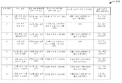
[0075]도 8b는, 제 1 정정 서브-모듈(603), 제 2 정정 서브-모듈(604), 및 분석 유닛(601)에 대한 입력 소스들을 포함하는 트랜시버(500)에 대한 예시적인 모드들 및 구성들을 설명하는 예시적인 테이블(850)을 도시한다. 테이블(850)은 또한 피드백 신호 선택기(551) 및 출력 선택기(550)와 연관된 셋팅들을 도시한다. 테이블(850)은 모든 가능한 동작 모드들 및 구성들의 철저한 리스트를 의미하는 것이 아니며, 대신 트랜시버(500)에 대한 예시적인 모드 및 구성들을 보여준다. 8b illustrates exemplary modes for a
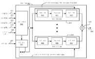
[0076]도 9는 도 2의 무선 디바이스(110)의 다른 예시적인 실시예인 디바이스(900)를 도시한다. 디바이스(900)는 트랜시버(910), 정정 모듈(920), 프로세서(930), 및 메모리(940)를 포함한다. 일부 실시예들에서, 트랜시버(910)는 도 4 및 도 5와 각각 관련하여 상술된 트랜시버(400) 또는 트랜시버(500)의 하나 또는 그 초과의 예시적인 실시예들과 유사할 수 있다. 다른 실시예들에서, 트랜시버(910)는 도 2와 관련하여 상술된 1차 트랜시버(220) 및/또는 2차 트랜시버(222)와 유사할 수 있다. 일부 실시예들에서, 트랜시버(910)는, 다중 반송파들(예를 들어, 반송파 주파수들)에 대한 동시 동작인 반송파 집성을 지원할 수 있는 다중-대역 트랜시버일 수 있다. 일 실시예에서, 트랜시버(910)는 상이한 반송파 주파수들을 통해 통신 신호들을 송신하고 수신하기 위한 제 1 송신기(903) 및 제 2 송신기(904)를 포함할 수 있다.[0076] FIG. 9 illustrates a device 900 that is another exemplary embodiment of the
[0077]정정 모듈(920)은 송신 통신 신호와 연관되는 하나 또는 그 초과의 손상들을 정정하기 위한 정정 신호(586)를 생성할 수 있다. 예를 들어, 일 실시예에서, 정정 모듈(920)은, 변조된 송신 통신 신호와 연관된 상호 변조 왜곡을 감소시키거나 감쇠시키기 위한 정정 신호(586)를 생성할 수 있다. 다른 실시예에서, 정정 모듈(920)은 송신 통신 신호를 등화하고 그리고/또는 사전 왜곡시키기 위한 정정 신호(586)를 생성할 수 있다. 정정 모듈(920)은 하나 또는 그 초과의 정정 서브-모듈들, 이를 테면, 제 1 정정 서브-모듈(603) 및/또는 제 2 정정 서브-모듈(604)(도 6a 참조)을 포함할 수 있다.[0077]
[0078]메모리(940)는 정정 모듈(920)에 대한 하나 또는 그 초과의 서브-모듈 셋팅들을 저장하기 위해 사용될 수 있는 룩업 테이블(942)을 포함할 수 있다. 일 실시예에서, 송신 통신 신호를 사전 왜곡시키는 것과 연관되는 서브-모듈 셋팅들이 룩업 테이블(942)에 저장될 수 있다. 다른 실시예에서, 송신 통신 신호를 등화하는 것과 연관되는 서브-모듈 셋팅들이 룩업 테이블(942)에 저장될 수 있다.[0078] The memory 940 may include a look-up table 942 that may be used to store one or more sub-module settings for the
[0079]메모리(940)는 또한, 다음 소프트웨어 모듈들:[0079] Memory 940 also includes the following software modules:
·트랜시버(910)를 동작시킬 주파수 대역들을 선택하기 위한 트랜시버 제어 소프트웨어(944); Transceiver control software 944 for selecting frequency bands for operating the transceiver 910;
·정정 모듈(920)에 대한 동작 모드들을 결정하기 위한 정정 모듈 제어 소프트웨어(946); 및Correction
·통신 신호를 분석하고 정정 모듈(920) 내에 포함된 정정 서브-모듈들에 대한 하나 또는 그 초과의 셋팅들을 결정하기 위한 신호 분석 소프트웨어(948)
를 저장할 수 있는 비일시적 컴퓨터 판독가능 저장 매체(예를 들어, 하나 또는 그 초과의 비휘발성 메모리 엘리먼트들, 이를 테면, EPROM, EEPROM, 플래시 메모리, 하드 드라이브 등)를 포함할 수 있다.(E.g., one or more non-volatile memory elements, such as EPROM, EEPROM, flash memory, hard drive, etc.) capable of storing a plurality of non-volatile memory elements.
각각의 소프트웨어 모듈은, 프로세서(930)에 의해 실행될 경우, 디바이스(900)로 하여금 대응하는 기능(들)을 수행하게 할 수 있는 프로그램 명령들을 포함한다. 따라서, 메모리(940)의 비일시적 컴퓨터 판독가능 저장 매체는 도 10의 동작들 모두 또는 동작들의 일 부분을 수행하기 위한 명령들을 포함할 수 있다. Each software module includes program instructions that, when executed by the processor 930, enable the device 900 to perform the corresponding function (s). Accordingly, the non-volatile computer readable storage medium of memory 940 may include all of the operations of FIG. 10 or instructions for performing a portion of the operations.
[0080]트랜시버(910), 정정 모듈(920), 및 메모리(940)에 커플링되는 프로세서(930)는 디바이스(900)에 (예를 들어, 메모리(940) 내에) 저장된 하나 또는 그 초과의 소프트웨어 프로그램들의 스크립트들 또는 명령들을 실행할 수 있는 임의의 하나 또는 그 초과의 적절한 프로세서들일 수 있다.The processor 930 coupled to the transceiver 910, the
[0081]프로세서(930)는 트랜시버(910)를 동작시킬 하나 또는 그 초과의 주파수 대역들을 선택하기 위한 트랜시버 제어 소프트웨어(944)를 실행시킬 수 있다. 예를 들어, 트랜시버 제어 소프트웨어(944)는 송신기(903)를 동작시키기 위해서는 2.4 GHz 주파수 대역을 선택할 수 있고 송신기(904)를 동작시키기 위해서는 900 MHz 주파수 대역을 선택할 수 있다. 다른 실시예들에서, 트랜시버(910)는 다른 주파수 대역들 내에서 동작할 수 있다.[0081] Processor 930 may execute transceiver control software 944 to select one or more frequency bands to operate transceiver 910. For example, the transceiver control software 944 may select the 2.4 GHz frequency band to operate the
[0082]프로세서(930)는 정정 모듈(920)에 대한 동작 모드들을 결정하기 위한 정정 모듈 제어 소프트웨어(946)를 실행시킬 수 있다. 예를 들어, 정정 모듈 제어 소프트웨어(946)는 제 1 송신 통신 신호 내의 상호 변조 왜곡을 감소시키기 위해 정정 모듈(920)을 제 1 동작 모드에서 동작시킬 수 있다. 다른 예에서, 정정 모듈 제어 소프트웨어(946)는 제 1 송신 통신 신호를 등화하기 위해 정정 모듈(920)을 제 5 동작 모드에서 동작시킬 수 있다. 본원에 나열된 동작 모드들은 단지 예시이며, 제한하려는 것은 아니다.[0082] The processor 930 may execute correction
[0083]프로세서(930)는 통신 신호를 분석하고 이 통신 신호에 기초하여 제 1 정정 서브-모듈(603) 및/또는 제 2 정정 서브-모듈(604)에 대한 하나 또는 그 초과의 서브-모듈 셋팅들을 결정하기 위해 신호 분석 소프트웨어(948)를 실행시킬 수 있다. 일부 실시예들에서, 신호 분석 소프트웨어(948)는 공격 신호를 분석하고, 희생 신호에 대한 그 공격 신호의 영향들을 감소시키거나 감쇠시키기 위한 정정 신호(586)를 생성하기 위해 서브-모듈 셋팅들을 결정할 수 있다. 다른 실시예들에서, 신호 분석 소프트웨어(948)는 통신 신호를 분석하고, 통신 신호를 등화하고 그리고/또는 사전 왜곡시키기 위한 정정 신호(586)를 생성하기 위해 서브-모듈 셋팅들을 결정할 수 있다.[0083] The processor 930 may be configured to analyze the communication signals and to provide one or
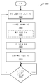
[0084]도 10은 일부 실시예들에 따른, 무선 디바이스(110)에 대한 예시적인 동작(1000)을 도시하는 예시적인 흐름도를 도시한다. 또한 도 5, 도 6, 도 8 및 도 9를 참조하면, 정정 모듈(560)의 동작 모드가 결정된다(1002). 일부 실시예들에서, 동작 모드는 원하는 정정 신호(586)에 기초할 수 있다. 예를 들어, 동작 모드는 적어도 부분적으로, 제 1 통신 신호와 연관된 상호 변조 왜곡을 감소시키거나 감쇠시키기 위한, 제 1 통신 신호를 등화하기 위한 그리고/또는 제 1 통신 신호를 사전 왜곡시키기 위한 정정 신호(586)에 의해 결정될 수 있다. 부가적으로, 일부 실시예들에서, 동작 모드는 또한 공격 신호 및 희생 신호에 의해 결정될 수 있다.[0084] FIG. 10 illustrates an exemplary flow chart illustrating an
[0085]다음으로, 서브-모듈 셋팅들이 동작 모드에 기초하여 결정된다(1004). 예를 들어, 정정 모듈(560)의 동작 모드는 제 1 통신 신호를 사전 왜곡시키도록 선택될 수 있다. 따라서, 제 1 통신 신호를 사전 왜곡시키기 위한 서브-모듈 셋팅들은 룩업 테이블(942)로부터 리트리빙되고, 제 1 통신 신호의 사전 왜곡을 수행하도록 정정 모듈(560)을 구성하는데 사용될 수 있다. 다른 예들에서, 다른 서브-모듈 셋팅들은 다른 동작 모드들에 기초하여 결정될 수 있다.[0085] Next, the sub-module settings are determined based on the operation mode (1004). For example, the operating mode of the
[0086]일부 실시예들에서, 서브-모듈 셋팅들(1004)을 결정하는 것은 또한 통신 신호의 선택적 분석을 포함할 수 있다(1006). 통신 신호의 분석은 서브-모듈 셋팅들의 결정을 도울 수 있다. 예를 들어, 정정 모듈(560)의 동작 모드가 공격 신호에 기인하는 상호 변조 왜곡을 감소시키거나 감쇠시키기 위한 정정 신호(586)를 생성하는 것이라면, 그 공격 신호는 분석 유닛(601)에 의해 분석될 수 있다. 다른 예에서, 정정 모듈(560)의 동작 모드가 제 1 통신 신호를 등화하기 위한 정정 신호(586)를 생성하는 것이라면, 제 1 통신 신호는 분석 유닛(601)에 의해 분석될 수 있다. 다른 예들에서, 다른 신호들이 분석 유닛(601)에 의해 분석될 수 있다.[0086] In some embodiments, determining the
[0087]다음으로, 정정 신호(586)가 생성된다(1008). 일부 실시예들에서, 정정 신호(586)는, 1004에서 결정된 서브-모듈 셋팅들에 의해 구성되는 하나 또는 그 초과의 정정 서브-모듈들(603 내지 604)에 의해 생성될 수 있다. 다음으로, 정정된 통신 신호가 생성된다(1010). 일부 실시예에서, 정정된 통신 신호는 정정 신호(586)와 통신 신호를 합산함으로써 생성될 수 있다.Next, a
[0088]다음으로, 서브-모듈 셋팅들의 업데이트가 결정된다(1012). 서브-모듈 셋팅들이 업데이트될 경우, 동작들은 1002로 진행한다. 서브-모듈 셋팅들이 변경되지 않을 경우, 동작들은 1012로 진행하여 서브-모듈 셋팅들이 업데이트될 것인지를 계속 체크한다.[0088] Next, an update of the sub-module settings is determined (1012). If the sub-module settings are updated, operations proceed to 1002. [ If the sub-module settings are not changed, operations proceed to 1012 to continue to check if the sub-module settings are to be updated.
[0089]본원에 개시된 실시예들과 관련하여 설명된 다양한 예시적인 로직 블록들, 모듈들 및 회로들은 범용 프로세서, DSP(digital signal processor), ASIC(application specific integrated circuit), FPGA(field programmable gate array) 또는 다른 프로그래밍 가능한 로직 디바이스, 이산 게이트 또는 트랜지스터 로직, 이산 하드웨어 컴포넌트들, 또는 본 명세서에서 설명된 기능들을 수행하도록 설계된 이들의 임의의 결합으로 구현되거나 이들에 의해 수행될 수 있다. 범용 프로세서는 마이크로프로세서일 수 있지만, 대안으로 프로세서는 임의의 종래 프로세서, 제어기, 마이크로제어기 또는 상태 머신일 수 있다. 프로세서는 또한 컴퓨팅 디바이스들의 결합, 예를 들어, DSP와 마이크로프로세서의 결합, 복수의 마이크로프로세서들, DSP 코어와 협력하는 하나 또는 그 초과의 마이크로프로세서들 또는 임의의 다른 이러한 구성으로서 구현될 수 있다.[0089] The various illustrative logical blocks, modules, and circuits described in connection with the embodiments disclosed herein may be implemented or performed with a general purpose processor, a digital signal processor (DSP), an application specific integrated circuit (ASIC), a field programmable gate array ) Or other programmable logic device, discrete gate or transistor logic, discrete hardware components, or any combination thereof designed to perform the functions described herein. A general purpose processor may be a microprocessor, but in the alternative, the processor may be any conventional processor, controller, microcontroller, or state machine. The processor may also be implemented as a combination of computing devices, e.g., a combination of a DSP and a microprocessor, a plurality of microprocessors, one or more microprocessors in cooperation with a DSP core, or any other such configuration.
[0090]하나 또는 그 초과의 예시적인 실시예들에서, 설명된 기능들은 하드웨어, 소프트웨어, 펌웨어, 또는 이들의 임의의 결합으로 구현될 수 있다. 소프트웨어로 구현되는 경우, 기능들은 하나 또는 그 초과의 명령들 또는 코드로서 컴퓨터 판독가능 매체 상에 저장되거나 또는 이로서 송신될 수 있다. 컴퓨터 판독가능 매체들은 컴퓨터 저장 매체들, 및 일 장소에서 다른 장소로 컴퓨터 프로그램의 이전을 용이하게 하는 임의의 매체들을 포함하는 통신 매체 둘 모두를 포함한다. 저장 매체는 컴퓨터에 의해 액세스될 수 있는 임의의 이용가능한 매체일 수 있다. 한정이 아닌 예시로, 이러한 컴퓨터 판독 가능 매체는 RAM, ROM, EEPROM, CD-ROM이나 다른 광 디스크 저장소, 자기 디스크 저장소 또는 다른 자기 저장 디바이스들, 또는 명령들이나 데이터 구조들의 형태로 원하는 프로그램 코드를 전달 또는 저장하는데 사용될 수 있으며 컴퓨터에 의해 액세스 가능한 임의의 다른 매체를 포함할 수 있다. 또한, 임의의 접속이 컴퓨터 판독 가능 매체로 적절히 지칭된다. 예를 들어, 소프트웨어가 동축 케이블, 광섬유 케이블, 연선, DSL(digital subscriber line), 또는 적외선, 라디오 및 마이크로파와 같은 무선 기술들을 사용하여 웹사이트, 서버 또는 다른 원격 소스로부터 전송된다면, 동축 케이블, 광섬유 케이블, 연선, DSL, 또는 적외선, 라디오 및 마이크로파와 같은 무선 기술들이 매체의 정의에 포함된다. 본원에서 이용된 바와 같은 디스크(disk) 및 디스크(disc)는 CD(compact disc), 레이저 디스크(laser disc), 광학 디스크(optical disc), DVD(digital versatile disc), 플로피 디스크(floppy disk) 및 블루레이 디스크(blu-ray disc)를 포함하고, 여기서, 디스크(disk)들은 통상 데이터를 자기적으로 재생하는 반면, 디스크(disc)들은 데이터를 레이저들로 광학적으로 재생한다. 상기의 것들의 결합들이 또한 컴퓨터 판독가능 매체들의 범위 내에 포함되어야 한다.[0090] In one or more exemplary embodiments, the functions described may be implemented in hardware, software, firmware, or any combination thereof. When implemented in software, the functions may be stored on or transmitted by one or more instructions or code on a computer readable medium. Computer-readable media includes both computer storage media and communication media including any medium that facilitates the transfer of a computer program from one place to another. The storage medium may be any available media that can be accessed by a computer. By way of example, and not limitation, such computer-readable media may carry any desired program code in the form of RAM, ROM, EEPROM, CD-ROM or other optical disk storage, magnetic disk storage or other magnetic storage devices, Or any other medium that can be used to store and be accessed by a computer. Also, any connection is properly referred to as a computer-readable medium. For example, if the software is transmitted from a web site, server, or other remote source using wireless technologies such as coaxial cable, fiber optic cable, twisted pair, digital subscriber line (DSL), or infrared, radio and microwave, Wireless technologies such as cable, twisted pair, DSL, or infrared, radio, and microwave are included in the definition of media. Disks and discs as used herein are intended to encompass discs and discs, such as compact discs (CD), laser discs, optical discs, digital versatile discs (DVDs), floppy disks, A blu-ray disc, wherein discs typically reproduce data magnetically, while discs optically reproduce data with lasers. Combinations of the above should also be included within the scope of computer readable media.
[0091]위의 명세서에서, 본 실시예들은, 본 명세서의 특정한 예시적 실시예들을 참조하여 설명되었다. 그러나, 첨부되는 청구항들에서 제시되는 바와 같은 본 개시내용의 더 넓은 사상 및 범위로부터 벗어나지 않고 본 명세서에 대해 다양한 수정들 및 변화들이 이루어질 수 있다는 것이 자명할 것이다. 따라서, 명세서 및 도면들은, 제한적 의미라기 보다는 예시적인 의미로서 간주된다.[0091] In the foregoing specification, the embodiments have been described with reference to specific exemplary embodiments thereof. It will, however, be evident that various modifications and changes may be made thereto without departing from the broader spirit and scope of the present disclosure as set forth in the appended claims. Accordingly, the specification and drawings are to be regarded in an illustrative rather than a restrictive sense.
Claims (20)
제 1 송신 통신 신호를 수정하기 위한 정정 신호의 제 1 부분을 생성하도록 구성된 제 1 정정 서브-모듈; 및
제 2 송신 통신 신호에 기초하여 상기 제 1 정정 서브-모듈을 제어하기 위한 서브-모듈 셋팅들을 결정하도록 구성된 분석 유닛을 포함하는, 장치.As an apparatus,
A first correction sub-module configured to generate a first portion of a correction signal for modifying a first transmission communication signal; And
And an analysis unit configured to determine sub-module settings for controlling the first correction sub-module based on the second transmission communication signal.
상기 제 1 송신 통신 신호는 제 1 송신기에 대한 디지털 기저대역 신호이고, 상기 제 2 송신 통신 신호는 제 2 송신기에 대한 디지털 기저대역 신호인, 장치.The method according to claim 1,
Wherein the first transmit communication signal is a digital baseband signal for a first transmitter and the second transmit communication signal is a digital baseband signal for a second transmitter.
복수의 통신 신호들로부터 상기 제 2 송신 통신 신호를 선택하도록 구성된 입력 선택기를 더 포함하는, 장치.The method according to claim 1,
Further comprising an input selector configured to select the second transmitted communication signal from the plurality of communication signals.
상기 정정 신호는 상기 제 1 송신 통신 신호와 연관된 상호 변조 왜곡을 감쇠시키도록 구성되는, 장치.The method according to claim 1,
Wherein the correction signal is configured to attenuate intermodulation distortion associated with the first transmitted communication signal.
상기 정정 신호는 상기 제 1 송신 통신 신호를 등화하도록 구성되는, 장치.The method according to claim 1,
Wherein the correction signal is configured to equalize the first transmit communication signal.
상기 정정 신호는 상기 제 1 송신 통신 신호를 사전 왜곡시키도록 구성되는, 장치.The method according to claim 1,
Wherein the correction signal is configured to pre-distort the first transmission communication signal.
상기 제 1 정정 서브-모듈은 상기 장치의 동작 모드에 기초하여 상기 정정 신호의 상기 제 1 부분을 생성하도록 구성되는, 장치.The method according to claim 1,
Wherein the first correction sub-module is configured to generate the first portion of the correction signal based on an operating mode of the device.
상기 장치의 동작 모드에 기초하여 모드 제어 신호를 생성하기 위한 제어 블록을 더 포함하는, 장치.8. The method of claim 7,
And a control block for generating a mode control signal based on an operating mode of the device.
상기 제 1 송신 통신 신호를 수정하기 위한 상기 정정 신호의 제 2 부분을 생성하도록 구성된 제 2 정정 서브-모듈을 더 포함하는, 장치.The method according to claim 1,
And a second correction sub-module configured to generate a second portion of the correction signal for modifying the first transmission communication signal.
상기 제 1 정정 서브-모듈은,
상기 제 2 송신 통신 신호와 연관된 위상을 수정하고;
상기 제 2 송신 통신 신호와 연관된 시간을 수정하고; 그리고
상기 제 2 송신 통신 신호와 연관된 진폭을 수정하도록 추가로 구성되는, 장치.The method according to claim 1,
The first correction sub-module comprises:
Modify a phase associated with the second transmitted communication signal;
Modify the time associated with the second transmitted communication signal; And
And to modify the amplitude associated with the second transmitted communication signal.
상기 분석 유닛은 상기 장치의 동작 모드에 기초하여 상기 제 1 정정 서브-모듈에 대한 모듈 셋팅들을 결정하도록 구성되는, 장치.The method according to claim 1,
Wherein the analysis unit is configured to determine module settings for the first correction sub-module based on an operating mode of the device.
상기 분석 유닛은 상기 제 2 송신 통신 신호를 분석하는 것에 기초하여 최초 정정 서브-모듈 셋팅들을 결정하도록 추가로 구성되는, 장치.The method according to claim 1,
Wherein the analysis unit is further configured to determine initial correction sub-module settings based on analyzing the second transmitted communication signal.
제 1 정정 서브-모듈을 통해 제 1 송신 통신 신호를 수정하기 위한 정정 신호의 제 1 부분을 생성하기 위한 수단; 및
제 2 송신 통신 신호에 기초하여 상기 제 1 정정 서브-모듈을 제어하기 위한 서브-모듈 셋팅들을 결정하기 위한 수단을 포함하는, 장치.As an apparatus,
Means for generating a first portion of a correction signal for modifying a first transmission communication signal via a first correction sub-module; And
And means for determining sub-module settings for controlling the first correction sub-module based on the second transmission communication signal.
상기 제 1 송신 통신 신호는 제 1 송신기에 대한 디지털 기저대역 신호이고, 상기 제 2 송신 통신 신호는 제 2 송신기에 대한 디지털 기저대역 신호인, 장치.14. The method of claim 13,
Wherein the first transmit communication signal is a digital baseband signal for a first transmitter and the second transmit communication signal is a digital baseband signal for a second transmitter.
복수의 통신 신호들로부터 상기 제 2 송신 통신 신호를 선택하기 위한 수단을 더 포함하는, 장치.14. The method of claim 13,
And means for selecting the second transmitted communication signal from the plurality of communication signals.
상기 정정 신호는 상기 제 1 송신 통신 신호와 연관된 상호 변조 왜곡을 감쇠시키도록 구성되는, 장치.14. The method of claim 13,
Wherein the correction signal is configured to attenuate intermodulation distortion associated with the first transmitted communication signal.
상기 정정 신호는 상기 제 1 송신 통신 신호를 등화하도록 구성되는, 장치.14. The method of claim 13,
Wherein the correction signal is configured to equalize the first transmit communication signal.
상기 정정 신호는 상기 제 1 송신 통신 신호를 사전 왜곡시키도록 구성되는, 장치.14. The method of claim 13,
Wherein the correction signal is configured to pre-distort the first transmission communication signal.
상기 정정 신호의 상기 제 1 부분은 상기 장치의 동작 모드에 기초하는, 장치.14. The method of claim 13,
Wherein the first portion of the correction signal is based on an operating mode of the device.
상기 명령들은, 장치의 프로세서에 의해 실행될 경우,
상기 장치로 하여금,
제 1 정정 서브-모듈에 의해, 제 1 송신 통신 신호를 수정하기 위한 정정 신호의 제 1 부분을 생성하게 하고; 그리고
분석 유닛에 의해, 제 2 송신 통신 신호에 기초하여 상기 제 1 정정 서브-모듈을 제어하기 위한 서브-모듈 셋팅들을 결정하게 하는, 명령들이 저장되는 비일시적 컴퓨터 판독가능 저장 매체.17. A non-transitory computer readable storage medium having stored thereon instructions,
The instructions, when executed by a processor of the device,
The apparatus comprising:
Generate, by the first correction sub-module, a first portion of the correction signal for modifying the first transmission communication signal; And
Module to determine, by an analysis unit, sub-module settings for controlling the first correction sub-module based on a second transmission communication signal.
Applications Claiming Priority (3)
| Application Number | Priority Date | Filing Date | Title |
|---|---|---|---|
| US14/668,823 | 2015-03-25 | ||
| US14/668,823 US9762266B2 (en) | 2015-03-25 | 2015-03-25 | Signal correction for carrier aggregation transceiver |
| PCT/US2016/021628 WO2016153787A1 (en) | 2015-03-25 | 2016-03-09 | Signal correction for carrier aggregation transceiver |
Publications (1)
| Publication Number | Publication Date |
|---|---|
| KR20170130431A true KR20170130431A (en) | 2017-11-28 |
Family
ID=55538659
Family Applications (1)
| Application Number | Title | Priority Date | Filing Date |
|---|---|---|---|
| KR1020177026911A KR20170130431A (en) | 2015-03-25 | 2016-03-09 | Signal Correction for Carrier-Aggregated Transceivers |
Country Status (6)
| Country | Link |
|---|---|
| US (1) | US9762266B2 (en) |
| EP (1) | EP3275081B1 (en) |
| JP (1) | JP2018509852A (en) |
| KR (1) | KR20170130431A (en) |
| CN (1) | CN107454994B (en) |
| WO (1) | WO2016153787A1 (en) |
Families Citing this family (11)
| Publication number | Priority date | Publication date | Assignee | Title |
|---|---|---|---|---|
| GB2544753B (en) * | 2015-11-24 | 2021-12-08 | Trw Ltd | Transceiver Circuits |
| US10666305B2 (en) * | 2015-12-16 | 2020-05-26 | Kumu Networks, Inc. | Systems and methods for linearized-mixer out-of-band interference mitigation |
| US9998160B2 (en) * | 2016-11-04 | 2018-06-12 | Mediatek Inc. | Methods for avoiding inter-modulation distortion and communications apparatuses utilizing the same |
| JP6837573B2 (en) | 2017-03-27 | 2021-03-03 | クム ネットワークス, インコーポレイテッドKumu Networks, Inc. | Linearity-enhanced mixer |
| US9985667B1 (en) | 2017-04-24 | 2018-05-29 | Mitsubishi Electric Research Laboratories, Inc. | Inter-band CA digital transmitter with multi-stage out-of-band noise canceller |
| US10469109B2 (en) * | 2017-09-19 | 2019-11-05 | Qualcomm Incorporated | Predistortion for transmitter with array |
| CN112335182B (en) | 2018-06-25 | 2022-02-08 | 株式会社村田制作所 | Front-end circuit |
| US10756774B2 (en) | 2018-12-18 | 2020-08-25 | Apple Inc. | Nonlinear interference cancellation |
| KR20210012235A (en) | 2019-07-24 | 2021-02-03 | 삼성전자주식회사 | Electronic device and wireless communication system thereof |
| US11606228B2 (en) | 2021-04-30 | 2023-03-14 | Hewlett Packard Enterprise Development Lp | Methods and systems for filter frequency response shift compensation for WLAN traffic |
| US11356133B1 (en) | 2021-04-30 | 2022-06-07 | Hewlett Packard Enterprise Development Lp | Methods and systems for filter frequency response shift compensation for WLAN traffic |
Family Cites Families (19)
| Publication number | Priority date | Publication date | Assignee | Title |
|---|---|---|---|---|
| JP3709316B2 (en) | 1999-05-28 | 2005-10-26 | 松下電器産業株式会社 | Communication apparatus and communication method |
| US7340265B2 (en) | 2002-02-28 | 2008-03-04 | Atheros Communications, Inc. | Method and apparatus for transient frequency distortion compensation |
| US6728517B2 (en) * | 2002-04-22 | 2004-04-27 | Cognio, Inc. | Multiple-input multiple-output radio transceiver |
| TWI251425B (en) * | 2002-11-15 | 2006-03-11 | Interdigital Tech Corp | Compensating for analog radio component impairments to relax specifications |
| DE602004027374D1 (en) * | 2003-06-04 | 2010-07-08 | St Ericsson Sa | REKTKONVERSIONSEMPFÄNGER |
| US7724840B2 (en) * | 2006-12-19 | 2010-05-25 | Crestcom, Inc. | RF transmitter with predistortion and method therefor |
| CN100578922C (en) | 2007-12-17 | 2010-01-06 | 华为技术有限公司 | High efficiency power amplifier |
| WO2010106752A1 (en) | 2009-03-19 | 2010-09-23 | パナソニック株式会社 | Distortion-correcting receiver and distortion correction method |
| US8331485B2 (en) | 2009-07-08 | 2012-12-11 | Qualcomm Incorporated | Spur cancellation in a digital baseband transmit signal using cancelling tones |
| US8326239B1 (en) | 2009-10-16 | 2012-12-04 | Qualcomm Atheros, Inc. | Power amplifier linearization using digital predistortion |
| US8442564B2 (en) * | 2011-01-13 | 2013-05-14 | Motorola Mobility Llc | Inter-modulation distortion reduction in multi-mode wireless communication terminal |
| US8885763B2 (en) | 2011-02-16 | 2014-11-11 | Analog Devices, Inc. | Digital pre-distortion |
| US8767869B2 (en) | 2011-08-18 | 2014-07-01 | Qualcomm Incorporated | Joint linear and non-linear cancellation of transmit self-jamming interference |
| US8817925B2 (en) | 2012-03-16 | 2014-08-26 | Qualcomm Incorporated | System and method for RF spur cancellation |
| CN103580609B (en) * | 2012-08-07 | 2017-03-01 | 晨星软件研发(深圳)有限公司 | The correcting unit of second order inter-modulation modulation distortion, system and bearing calibration |
| US8917792B2 (en) * | 2012-12-12 | 2014-12-23 | Motorola Mobility Llc | Method and apparatus for the cancellation of intermodulation and harmonic distortion in a baseband receiver |
| WO2014136437A1 (en) | 2013-03-07 | 2014-09-12 | 日本電気株式会社 | Wireless transmission device and wireless transmission method |
| US9231801B2 (en) | 2013-03-15 | 2016-01-05 | Qualcomm Incorporated | Adaptive non-linear interference cancellation for intermodulation distortion |
| JP2014192670A (en) * | 2013-03-27 | 2014-10-06 | Nec Casio Mobile Communications Ltd | Radio device, its control method, and program |
-
2015
- 2015-03-25 US US14/668,823 patent/US9762266B2/en active Active
-
2016
- 2016-03-09 KR KR1020177026911A patent/KR20170130431A/en unknown
- 2016-03-09 CN CN201680016982.0A patent/CN107454994B/en not_active Expired - Fee Related
- 2016-03-09 WO PCT/US2016/021628 patent/WO2016153787A1/en active Application Filing
- 2016-03-09 EP EP16710083.3A patent/EP3275081B1/en active Active
- 2016-03-09 JP JP2017549646A patent/JP2018509852A/en not_active Ceased
Also Published As
| Publication number | Publication date |
|---|---|
| JP2018509852A (en) | 2018-04-05 |
| EP3275081B1 (en) | 2019-06-12 |
| CN107454994B (en) | 2020-01-17 |
| US20160285484A1 (en) | 2016-09-29 |
| WO2016153787A1 (en) | 2016-09-29 |
| US9762266B2 (en) | 2017-09-12 |
| CN107454994A (en) | 2017-12-08 |
| EP3275081A1 (en) | 2018-01-31 |
Similar Documents
| Publication | Publication Date | Title |
|---|---|---|
| EP3275081B1 (en) | Signal correction for carrier aggregation transceiver | |
| US10291384B2 (en) | Transceiver and method for reducing a self-interference of a transceiver | |
| US20220286266A1 (en) | Zero division duplexing mimo radio with adaptable rf and/or baseband cancellation | |
| US8964821B2 (en) | Shared feedback for adaptive transmitter pre-distortion | |
| RU2664392C2 (en) | Method and device for interference suppression | |
| JP6585168B2 (en) | Intermodulation distortion canceller for use in multicarrier transmitters. | |
| US8204456B2 (en) | Systems and methods for spurious emission cancellation | |
| US9438284B2 (en) | Non-linear interference cancellation for multiple receiver antennas | |
| US9100110B2 (en) | Non-linear interference cancellation with multiple aggressors | |
| US10992335B2 (en) | Methods and transceivers for reducing a distortion component within a baseband receive signal | |
| US10230421B2 (en) | Receiver and a method for reducing a distortion component within a baseband receive signal | |
| US20170237454A1 (en) | Non-linear product detection and cancellation in a wireless device | |
| JP2012060433A (en) | Transmitter-receiver, rfic for mobile phone terminal using the same, and base station for mobile phone |