KR20170123820A - Display apparatus - Google Patents
Display apparatus Download PDFInfo
- Publication number
- KR20170123820A KR20170123820A KR1020160052881A KR20160052881A KR20170123820A KR 20170123820 A KR20170123820 A KR 20170123820A KR 1020160052881 A KR1020160052881 A KR 1020160052881A KR 20160052881 A KR20160052881 A KR 20160052881A KR 20170123820 A KR20170123820 A KR 20170123820A
- Authority
- KR
- South Korea
- Prior art keywords
- rear cover
- light guide
- guide plate
- heat sink
- display panel
- Prior art date
Links
- 239000000758 substrate Substances 0.000 claims abstract description 109
- 230000003287 optical effect Effects 0.000 claims description 40
- 230000008878 coupling Effects 0.000 claims description 32
- 238000010168 coupling process Methods 0.000 claims description 32
- 238000005859 coupling reaction Methods 0.000 claims description 32
- 230000003014 reinforcing effect Effects 0.000 claims description 32
- 238000000034 method Methods 0.000 claims description 18
- 239000000463 material Substances 0.000 claims description 6
- 239000007769 metal material Substances 0.000 claims description 5
- 238000003825 pressing Methods 0.000 claims description 3
- 230000005855 radiation Effects 0.000 abstract description 3
- 229910052782 aluminium Inorganic materials 0.000 description 7
- XAGFODPZIPBFFR-UHFFFAOYSA-N aluminium Chemical compound [Al] XAGFODPZIPBFFR-UHFFFAOYSA-N 0.000 description 7
- 230000017525 heat dissipation Effects 0.000 description 5
- 238000003780 insertion Methods 0.000 description 5
- 230000037431 insertion Effects 0.000 description 5
- 239000004973 liquid crystal related substance Substances 0.000 description 4
- 230000000694 effects Effects 0.000 description 3
- 230000014509 gene expression Effects 0.000 description 2
- 238000012986 modification Methods 0.000 description 2
- 230000004048 modification Effects 0.000 description 2
- 210000000080 chela (arthropods) Anatomy 0.000 description 1
- 230000005672 electromagnetic field Effects 0.000 description 1
- 239000011521 glass Substances 0.000 description 1
- 230000001678 irradiating effect Effects 0.000 description 1
- 230000007257 malfunction Effects 0.000 description 1
- 238000004519 manufacturing process Methods 0.000 description 1
- 238000007789 sealing Methods 0.000 description 1
Images


Classifications
-
- G—PHYSICS
- G02—OPTICS
- G02F—OPTICAL DEVICES OR ARRANGEMENTS FOR THE CONTROL OF LIGHT BY MODIFICATION OF THE OPTICAL PROPERTIES OF THE MEDIA OF THE ELEMENTS INVOLVED THEREIN; NON-LINEAR OPTICS; FREQUENCY-CHANGING OF LIGHT; OPTICAL LOGIC ELEMENTS; OPTICAL ANALOGUE/DIGITAL CONVERTERS
- G02F1/00—Devices or arrangements for the control of the intensity, colour, phase, polarisation or direction of light arriving from an independent light source, e.g. switching, gating or modulating; Non-linear optics
- G02F1/01—Devices or arrangements for the control of the intensity, colour, phase, polarisation or direction of light arriving from an independent light source, e.g. switching, gating or modulating; Non-linear optics for the control of the intensity, phase, polarisation or colour
- G02F1/13—Devices or arrangements for the control of the intensity, colour, phase, polarisation or direction of light arriving from an independent light source, e.g. switching, gating or modulating; Non-linear optics for the control of the intensity, phase, polarisation or colour based on liquid crystals, e.g. single liquid crystal display cells
- G02F1/133—Constructional arrangements; Operation of liquid crystal cells; Circuit arrangements
- G02F1/1333—Constructional arrangements; Manufacturing methods
- G02F1/133308—Support structures for LCD panels, e.g. frames or bezels
-
- G—PHYSICS
- G02—OPTICS
- G02B—OPTICAL ELEMENTS, SYSTEMS OR APPARATUS
- G02B6/00—Light guides; Structural details of arrangements comprising light guides and other optical elements, e.g. couplings
- G02B6/0001—Light guides; Structural details of arrangements comprising light guides and other optical elements, e.g. couplings specially adapted for lighting devices or systems
- G02B6/0011—Light guides; Structural details of arrangements comprising light guides and other optical elements, e.g. couplings specially adapted for lighting devices or systems the light guides being planar or of plate-like form
- G02B6/0081—Mechanical or electrical aspects of the light guide and light source in the lighting device peculiar to the adaptation to planar light guides, e.g. concerning packaging
- G02B6/0085—Means for removing heat created by the light source from the package
-
- G—PHYSICS
- G02—OPTICS
- G02F—OPTICAL DEVICES OR ARRANGEMENTS FOR THE CONTROL OF LIGHT BY MODIFICATION OF THE OPTICAL PROPERTIES OF THE MEDIA OF THE ELEMENTS INVOLVED THEREIN; NON-LINEAR OPTICS; FREQUENCY-CHANGING OF LIGHT; OPTICAL LOGIC ELEMENTS; OPTICAL ANALOGUE/DIGITAL CONVERTERS
- G02F1/00—Devices or arrangements for the control of the intensity, colour, phase, polarisation or direction of light arriving from an independent light source, e.g. switching, gating or modulating; Non-linear optics
- G02F1/01—Devices or arrangements for the control of the intensity, colour, phase, polarisation or direction of light arriving from an independent light source, e.g. switching, gating or modulating; Non-linear optics for the control of the intensity, phase, polarisation or colour
- G02F1/13—Devices or arrangements for the control of the intensity, colour, phase, polarisation or direction of light arriving from an independent light source, e.g. switching, gating or modulating; Non-linear optics for the control of the intensity, phase, polarisation or colour based on liquid crystals, e.g. single liquid crystal display cells
- G02F1/133—Constructional arrangements; Operation of liquid crystal cells; Circuit arrangements
- G02F1/1333—Constructional arrangements; Manufacturing methods
- G02F1/133308—Support structures for LCD panels, e.g. frames or bezels
- G02F1/133314—Back frames
-
- G—PHYSICS
- G02—OPTICS
- G02F—OPTICAL DEVICES OR ARRANGEMENTS FOR THE CONTROL OF LIGHT BY MODIFICATION OF THE OPTICAL PROPERTIES OF THE MEDIA OF THE ELEMENTS INVOLVED THEREIN; NON-LINEAR OPTICS; FREQUENCY-CHANGING OF LIGHT; OPTICAL LOGIC ELEMENTS; OPTICAL ANALOGUE/DIGITAL CONVERTERS
- G02F1/00—Devices or arrangements for the control of the intensity, colour, phase, polarisation or direction of light arriving from an independent light source, e.g. switching, gating or modulating; Non-linear optics
- G02F1/01—Devices or arrangements for the control of the intensity, colour, phase, polarisation or direction of light arriving from an independent light source, e.g. switching, gating or modulating; Non-linear optics for the control of the intensity, phase, polarisation or colour
- G02F1/13—Devices or arrangements for the control of the intensity, colour, phase, polarisation or direction of light arriving from an independent light source, e.g. switching, gating or modulating; Non-linear optics for the control of the intensity, phase, polarisation or colour based on liquid crystals, e.g. single liquid crystal display cells
- G02F1/133—Constructional arrangements; Operation of liquid crystal cells; Circuit arrangements
- G02F1/1333—Constructional arrangements; Manufacturing methods
- G02F1/133308—Support structures for LCD panels, e.g. frames or bezels
- G02F1/13332—Front frames
-
- G—PHYSICS
- G02—OPTICS
- G02F—OPTICAL DEVICES OR ARRANGEMENTS FOR THE CONTROL OF LIGHT BY MODIFICATION OF THE OPTICAL PROPERTIES OF THE MEDIA OF THE ELEMENTS INVOLVED THEREIN; NON-LINEAR OPTICS; FREQUENCY-CHANGING OF LIGHT; OPTICAL LOGIC ELEMENTS; OPTICAL ANALOGUE/DIGITAL CONVERTERS
- G02F1/00—Devices or arrangements for the control of the intensity, colour, phase, polarisation or direction of light arriving from an independent light source, e.g. switching, gating or modulating; Non-linear optics
- G02F1/01—Devices or arrangements for the control of the intensity, colour, phase, polarisation or direction of light arriving from an independent light source, e.g. switching, gating or modulating; Non-linear optics for the control of the intensity, phase, polarisation or colour
- G02F1/13—Devices or arrangements for the control of the intensity, colour, phase, polarisation or direction of light arriving from an independent light source, e.g. switching, gating or modulating; Non-linear optics for the control of the intensity, phase, polarisation or colour based on liquid crystals, e.g. single liquid crystal display cells
- G02F1/133—Constructional arrangements; Operation of liquid crystal cells; Circuit arrangements
- G02F1/1333—Constructional arrangements; Manufacturing methods
- G02F1/133382—Heating or cooling of liquid crystal cells other than for activation, e.g. circuits or arrangements for temperature control, stabilisation or uniform distribution over the cell
- G02F1/133385—Heating or cooling of liquid crystal cells other than for activation, e.g. circuits or arrangements for temperature control, stabilisation or uniform distribution over the cell with cooling means, e.g. fans
-
- G—PHYSICS
- G02—OPTICS
- G02F—OPTICAL DEVICES OR ARRANGEMENTS FOR THE CONTROL OF LIGHT BY MODIFICATION OF THE OPTICAL PROPERTIES OF THE MEDIA OF THE ELEMENTS INVOLVED THEREIN; NON-LINEAR OPTICS; FREQUENCY-CHANGING OF LIGHT; OPTICAL LOGIC ELEMENTS; OPTICAL ANALOGUE/DIGITAL CONVERTERS
- G02F1/00—Devices or arrangements for the control of the intensity, colour, phase, polarisation or direction of light arriving from an independent light source, e.g. switching, gating or modulating; Non-linear optics
- G02F1/01—Devices or arrangements for the control of the intensity, colour, phase, polarisation or direction of light arriving from an independent light source, e.g. switching, gating or modulating; Non-linear optics for the control of the intensity, phase, polarisation or colour
- G02F1/13—Devices or arrangements for the control of the intensity, colour, phase, polarisation or direction of light arriving from an independent light source, e.g. switching, gating or modulating; Non-linear optics for the control of the intensity, phase, polarisation or colour based on liquid crystals, e.g. single liquid crystal display cells
- G02F1/133—Constructional arrangements; Operation of liquid crystal cells; Circuit arrangements
- G02F1/1333—Constructional arrangements; Manufacturing methods
- G02F1/1335—Structural association of cells with optical devices, e.g. polarisers or reflectors
- G02F1/133524—Light-guides, e.g. fibre-optic bundles, louvered or jalousie light-guides
-
- G—PHYSICS
- G02—OPTICS
- G02F—OPTICAL DEVICES OR ARRANGEMENTS FOR THE CONTROL OF LIGHT BY MODIFICATION OF THE OPTICAL PROPERTIES OF THE MEDIA OF THE ELEMENTS INVOLVED THEREIN; NON-LINEAR OPTICS; FREQUENCY-CHANGING OF LIGHT; OPTICAL LOGIC ELEMENTS; OPTICAL ANALOGUE/DIGITAL CONVERTERS
- G02F1/00—Devices or arrangements for the control of the intensity, colour, phase, polarisation or direction of light arriving from an independent light source, e.g. switching, gating or modulating; Non-linear optics
- G02F1/01—Devices or arrangements for the control of the intensity, colour, phase, polarisation or direction of light arriving from an independent light source, e.g. switching, gating or modulating; Non-linear optics for the control of the intensity, phase, polarisation or colour
- G02F1/13—Devices or arrangements for the control of the intensity, colour, phase, polarisation or direction of light arriving from an independent light source, e.g. switching, gating or modulating; Non-linear optics for the control of the intensity, phase, polarisation or colour based on liquid crystals, e.g. single liquid crystal display cells
- G02F1/133—Constructional arrangements; Operation of liquid crystal cells; Circuit arrangements
- G02F1/1333—Constructional arrangements; Manufacturing methods
- G02F1/1335—Structural association of cells with optical devices, e.g. polarisers or reflectors
- G02F1/1336—Illuminating devices
- G02F1/133615—Edge-illuminating devices, i.e. illuminating from the side
-
- G—PHYSICS
- G02—OPTICS
- G02B—OPTICAL ELEMENTS, SYSTEMS OR APPARATUS
- G02B6/00—Light guides; Structural details of arrangements comprising light guides and other optical elements, e.g. couplings
- G02B6/0001—Light guides; Structural details of arrangements comprising light guides and other optical elements, e.g. couplings specially adapted for lighting devices or systems
- G02B6/0011—Light guides; Structural details of arrangements comprising light guides and other optical elements, e.g. couplings specially adapted for lighting devices or systems the light guides being planar or of plate-like form
- G02B6/0033—Means for improving the coupling-out of light from the light guide
- G02B6/005—Means for improving the coupling-out of light from the light guide provided by one optical element, or plurality thereof, placed on the light output side of the light guide
- G02B6/0051—Diffusing sheet or layer
-
- G—PHYSICS
- G02—OPTICS
- G02B—OPTICAL ELEMENTS, SYSTEMS OR APPARATUS
- G02B6/00—Light guides; Structural details of arrangements comprising light guides and other optical elements, e.g. couplings
- G02B6/0001—Light guides; Structural details of arrangements comprising light guides and other optical elements, e.g. couplings specially adapted for lighting devices or systems
- G02B6/0011—Light guides; Structural details of arrangements comprising light guides and other optical elements, e.g. couplings specially adapted for lighting devices or systems the light guides being planar or of plate-like form
- G02B6/0081—Mechanical or electrical aspects of the light guide and light source in the lighting device peculiar to the adaptation to planar light guides, e.g. concerning packaging
- G02B6/0086—Positioning aspects
- G02B6/0088—Positioning aspects of the light guide or other optical sheets in the package
-
- G—PHYSICS
- G02—OPTICS
- G02B—OPTICAL ELEMENTS, SYSTEMS OR APPARATUS
- G02B6/00—Light guides; Structural details of arrangements comprising light guides and other optical elements, e.g. couplings
- G02B6/0001—Light guides; Structural details of arrangements comprising light guides and other optical elements, e.g. couplings specially adapted for lighting devices or systems
- G02B6/0011—Light guides; Structural details of arrangements comprising light guides and other optical elements, e.g. couplings specially adapted for lighting devices or systems the light guides being planar or of plate-like form
- G02B6/0081—Mechanical or electrical aspects of the light guide and light source in the lighting device peculiar to the adaptation to planar light guides, e.g. concerning packaging
- G02B6/0086—Positioning aspects
- G02B6/009—Positioning aspects of the light source in the package
-
- G—PHYSICS
- G02—OPTICS
- G02F—OPTICAL DEVICES OR ARRANGEMENTS FOR THE CONTROL OF LIGHT BY MODIFICATION OF THE OPTICAL PROPERTIES OF THE MEDIA OF THE ELEMENTS INVOLVED THEREIN; NON-LINEAR OPTICS; FREQUENCY-CHANGING OF LIGHT; OPTICAL LOGIC ELEMENTS; OPTICAL ANALOGUE/DIGITAL CONVERTERS
- G02F1/00—Devices or arrangements for the control of the intensity, colour, phase, polarisation or direction of light arriving from an independent light source, e.g. switching, gating or modulating; Non-linear optics
- G02F1/01—Devices or arrangements for the control of the intensity, colour, phase, polarisation or direction of light arriving from an independent light source, e.g. switching, gating or modulating; Non-linear optics for the control of the intensity, phase, polarisation or colour
- G02F1/13—Devices or arrangements for the control of the intensity, colour, phase, polarisation or direction of light arriving from an independent light source, e.g. switching, gating or modulating; Non-linear optics for the control of the intensity, phase, polarisation or colour based on liquid crystals, e.g. single liquid crystal display cells
- G02F1/133—Constructional arrangements; Operation of liquid crystal cells; Circuit arrangements
- G02F1/1333—Constructional arrangements; Manufacturing methods
- G02F1/1335—Structural association of cells with optical devices, e.g. polarisers or reflectors
- G02F1/1336—Illuminating devices
- G02F1/133628—Illuminating devices with cooling means
-
- G02F2001/133314—
-
- G02F2001/13332—
Abstract
Description
본 발명은 섀시가 개선된 디스플레이 장치에 관한 것이다. The present invention relates to a display device with improved chassis.
일반적으로 디스플레이 장치는 화면을 표시하는 장치로, 모니터나 텔레비전이 이에 포함된다. 디스플레이 장치는 유기 발광 다이오드(OLED: Organic Light-Emitting Diode)와 같은 자발광 디스플레이 패널과, 액정 디스플레이(LCD, liquid crystal display) 패널과 같은 수광 디스플레이 패널이 사용된다.Generally, a display device is a device for displaying a screen, which includes a monitor and a television. A display device uses a self-luminous display panel such as an organic light-emitting diode (OLED) and a light-receiving display panel such as a liquid crystal display (LCD) panel.
본 발명은 수광 디스플레이 패널에 관한 것으로 액정패널로 이루어져 화면이 표시되는 디스플레이 패널과, 디스플레이 패널의 후방측에 배치된 백라이트 유닛을 포함한다. 또한 백라이트 유닛에서 조사되는 광을 디스플레이 패널 측으로 조사하기 위해 광학시트, 도광판 등의 구성을 포함할 수 있다.The present invention relates to a light receiving display panel, including a display panel formed of a liquid crystal panel and displaying a screen, and a backlight unit disposed on a rear side of the display panel. Further, it may include an optical sheet, a light guide plate, and the like to irradiate the light emitted from the backlight unit toward the display panel.
상술한 디스플레이 장치의 구성들은 탑섀시와 바텀섀시로 구성되는 섀시와 탑섀시와 바텀섀시 사이에 배치되는 미들몰드에 의해 지지될 수 있다.The above-described configurations of the display device can be supported by a chassis composed of a top chassis and a bottom chassis, and a middle mold disposed between the top chassis and the bottom chassis.
최근의 디스플레이 장치들이 슬림화되는 추세에 있어서 상술한 미들몰드와 바텀섀시를 모두 포함하는 경우 디스플레이 장치의 두께가 증가하고 원가가 상승하는 문제가 발생할 수 있다.In recent trends of display devices becoming slimmer, the thickness of the display device may increase and the cost may increase when the display device includes both the middle mold and the bottom chassis.
본 발명의 일측면은 미들몰드와 바텀섀시를 포함하지 않고 탑섀시와 리어커버로 디스플레이 패널 등의 구성을 지지하는 디스플레이 장치를 제공한다.One aspect of the present invention provides a display device that does not include a middle mold and a bottom chassis but supports a configuration such as a display panel with a top chassis and a rear cover.
본 발명의 다른 측면은 탑섀시와 리어커버 사이에 방열을 위해 마련되는 히트 싱크를 포함하는 디스플레이 장치를 제공한다.Another aspect of the present invention provides a display device including a heat sink provided between the top chassis and the rear cover for radiating heat.
본 발명의 사상에 따른 디스플레이 장치는 디스플레이 패널과 상기 디스플레이 패널의 전방에 마련되는 탑 섀시와 상기 디스플레이 패널의 후방에 배치되고 상기 탑 섀시에 지지되는 광학시트와 상기 광학시트 후방에 배치되는 도광판과 상기 도광판의 측면에 배치되어 상기 도광판에 광을 조사하는 LED 기판과 상기 디스플레이 패널의 외관을 형성하고 상기 탑 섀시의 후방에서 상기 탑 섀시에 결합되고 상기 도광판을 상기 탑섀시측으로 가압하는 리어 커버와 상기 LED기판에서 발생하는 열을 방열하도록 상기 LED기판과 연결되고 상기도광판과 상기 리어 커버 사이에 배치되는 히트 싱크(heat sink)를 포함한다. A display device according to the present invention includes a display panel, a top chassis disposed in front of the display panel, an optical sheet disposed behind the display panel and supported by the top chassis, a light guide plate disposed behind the optical sheet, A rear cover which is disposed on a side surface of the light guide plate and irradiates light to the light guide plate, a rear cover which forms an outer surface of the display panel and is coupled to the top chassis at the rear of the top chassis and presses the light guide plate toward the top chassis, And a heat sink connected to the LED substrate to dissipate heat generated from the substrate and disposed between the light guide plate and the rear cover.
또한 상기 리어 커버는 플라스틱 재질을 포함한다.Further, the rear cover includes a plastic material.
또한 상기 히트 싱크는 상기 LED기판의 길이 방향과 대응되는 방향으로 연장되는 제 1변과 상기 제 1변보다 길이가 짧은 제 2변을 포함하는 플레이트 형상으로 마련된다.The heat sink is provided in a plate shape including a first side extending in a direction corresponding to a longitudinal direction of the LED substrate and a second side having a length shorter than the first side.
또한 상기 히트 싱크의 넓이는 상기 도광판의 넓이보다 작다.And the width of the heat sink is smaller than the width of the light guide plate.
또한 상기 리어 커버의 강성을 보강하도록 상기 리어 커버와 결합되는 보강부재를 더 포함하고, 상기 보강부재의 적어도 일측은 상기 히트 싱크와 접한다.And a reinforcing member coupled to the rear cover to reinforce the rigidity of the rear cover, wherein at least one side of the reinforcing member contacts the heat sink.
또한 상기 리어 커버는 상기 탑 섀시 측으로 돌출되고 상기 도광판이 상기 탑 섀시에 지지되도록 상기 도광판을 상기 탑 섀시 측으로 가압하는 복수의 리브를 포함한다.The rear cover further includes a plurality of ribs protruding toward the top chassis and pressing the light guide plate toward the top chassis so that the light guide plate is supported by the top chassis.
또한 상기 탑 섀시는 상기 광학시트가 걸리도록 상기 광학시트 측으로 돌출되는 걸이부를 포함하고, 상기 광학시트는 상기 걸이부가 관통되도록 마련되는 걸이홀을 포함한다.The top chassis includes a hook portion protruding toward the optical sheet so as to catch the optical sheet, and the optical sheet includes a hook hole provided to allow the hook portion to penetrate.
또한 상기 도광판 후방에 배치되는 반사시트를 더 포함하고, 상기 반사시트는 상기 걸이부에 걸려 상기 탑 섀시에 지지된다.And a reflective sheet disposed behind the light guide plate, wherein the reflective sheet is held by the hook portion and supported by the top chassis.
또한 상기 탑 섀시는 상기 도광판이 지지되도록 상기 도광판 측으로 돌출되는 도광판 지지부를 포함하고, 상기 도광판 지지부는 상기 디스플레이 패널과 상기 광학패널의 두께의 합과 대응되는 길이로 돌출된다.The top chassis includes a light guide plate supporting part protruding toward the light guide plate to support the light guide plate, and the light guide plate supporting part protrudes to a length corresponding to the sum of thicknesses of the display panel and the optical panel.
또한 상기 탑 섀시는 상기 히트 싱크가 지지되도록 상기 히트 싱크 측으로 돌출되는 끼움 돌기를 포함하고, 상기 히트 싱크는 상기 끼움 돌기와 끼움 결합되도록 마련되는 끼움홈을 포함한다.Further, the top chassis includes a fitting protrusion protruded toward the heat sink so as to support the heat sink, and the heat sink includes a fitting groove fitted to the fitting protrusion.
또한 전장품이 실장되는 전장품 기판을 더 포함하고, 상기 전장품 기판은 상기 리어 커버에 결합된다.And an electrical component substrate on which an electrical component is mounted, and the electrical component substrate is coupled to the rear cover.
또한 전장품 기판의 일측에는 상기 전장품 기판의 넓이와 대응되는 넓이로 마련되는 결합 플레이트가 배치된다.And an engaging plate provided on one side of the electric component substrate, the engaging plate having a width corresponding to the width of the electric component substrate.
또한 상기 전장품 기판은 상기 도광판과 상기 리어 커버 사이에 배치된다.And the electric component substrate is disposed between the light guide plate and the rear cover.
또한 상기 전장품 기판은 상기 리어 커버의 후방에 배치되고, 상기 리어커버는 상기 전장품 기판을 커버하는 보조 커버를 포함한다.The electric component substrate is disposed behind the rear cover, and the rear cover includes an auxiliary cover covering the electrical component substrate.
또한 상기 결합플레이트는 상기 히트 싱크와 연결된다.The coupling plate is connected to the heat sink.
본 발명의 사상에 따른 디스플레이 장치는 디스플레이 패널과 상기 디스플레이 패널의 전방에 마련되는 탑 섀시와 상기 디스플레이 패널의 후방에 마련되고 상기 탑 섀시와 결합하는 리어 커버와 상기 탑 섀시와 상기 리어 커버 사이에 배치되어 지지되는 광학시트와 도광판과 상기 도광판에 광을 조사하도록 상기 도광판의 측방에 배치되는 LED 기판과 상기 LED기판에서 발생하는 열을 방열하도록 상기 LED기판과 연결되는 히트 싱크(heat sink)와 상기 리어 커버의 강성을 보강하도록 상기 리어 커버와 결합되고 상기 히트 싱크와 연결되는 보강 부재를 포함한다.A display device according to an embodiment of the present invention includes a display panel, a top chassis provided in front of the display panel, a rear cover provided at the rear of the display panel and engaged with the top chassis, and a rear cover disposed between the top chassis and the rear cover A heat sink connected to the LED substrate to dissipate heat generated in the LED substrate, and a heat sink connected to the LED substrate, wherein the heat sink includes a light guide plate, a light guide plate, an LED substrate disposed on the side of the light guide plate, And a reinforcing member coupled to the rear cover to reinforce the rigidity of the cover and connected to the heat sink.
또한 상기 리어 커버에 결합되고 전장품이 실장되는 전장품 기판을 더 포함하고, 상기 전장품 기판의 일측에는 상기 전장품 기판에서 발생하는 전자파를 감소시키는 결합 플레이트가 배치된다.And an electrical component board coupled to the rear cover and to which electrical components are mounted, and a coupling plate for reducing electromagnetic waves generated from the electrical component substrate is disposed on one side of the electrical component substrate.
또한 상기 결합 플레이트는 상기 히트 싱크과 상기 보강 부재 중 적어도 하나와 연결된다.The coupling plate is connected to at least one of the heat sink and the reinforcing member.
또한 상기 탑 섀시와 상기 리어 커버는 후크 결합된다.Further, the top chassis and the rear cover are hooked.
본 발명의 사상에 따른 디스플레이 장치는 디스플레이 패널과 상기 디스플레이 패널의 전방에 마련되는 섀시와 상기 디스플레이 패널의 외관을 형성하고 상기 디스플레이 패널의 후방에서 상기 섀시와 결합하고 플라스틱 재질을 포함하는 리어 커버와 상기 섀시와 상기 리어 커버에 의해 지지되는 도광판과 상기 도광판에 광을 조사하는 LED기판과 상기LED기판과 연결되고 상기 디스플레이 패널과 상기 리어 커버 사이에 배치되는 금속 재질을 포함하는 플레이트를 포함한다.A display device according to an embodiment of the present invention includes a display panel, a chassis provided in front of the display panel, a rear cover which forms an outer surface of the display panel and is coupled to the chassis at the rear of the display panel, And a plate including a chassis, a light guide plate supported by the rear cover, an LED substrate for emitting light to the light guide plate, and a metal material connected to the LED substrate and disposed between the display panel and the rear cover.
본 발명은 미들몰드와 바텀섀시를 포함하지 않아 디스플레이 장치의 두께를 얇게 구현할 수 있고, 원가를 절감할 수 있는 효과가 있다. Since the present invention does not include a middle mold and a bottom chassis, the thickness of the display device can be reduced and the cost can be reduced.
또한 바텀섀시가 없음에도 히트 싱크를 포함하여 LED기판에서 발생하는 열을 효과적으로 방열할 수 있다.In addition, even without the bottom chassis, the heat generated from the LED substrate can be effectively dissipated, including the heat sink.
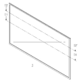
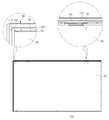
도 1은 본 발명의 일 실시예에 따른 디스플레이 장치의 사시도이다.
도 2는 본 발명의 일 실시예에 따른 디스플레이 장치의 분해사시도이다.
도 3은 도 1에 표시된 I1-I1선에 따른 측단면도이다.
도 4는 본 발명의 일 실시예에 따른 디스플레이 장치의 탑 섀시에 대한 배면도이다.
도 5는 본 발명의 일 실시예에 의한 디스플레이 장치의 탑 섀시와 일부 구성에 대한 배면도이다.
도 6은 본 발명의 일 실시예에 의한 디스플레이 장치의 탑 섀시와 일부 구성에 대한 배면도이다.
도 7은 본 발명의 일 실시예에 따른 디스플레이 장치의 탑 섀시와 일부 구성에 대한 배면도이다.
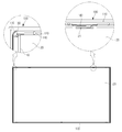
도 8은 본 발명의 일 실시예에 따른 디스플레이 장치의 LED기판과 히트 싱크에 대한 사시도이다.
도 9는 본 발명의 일 실시예에 의한 디스플레이 장치의 리어 커버와 일부 구성에 대한 사시도이다.
도 10은 본 발명의 일 실시예에 의한 디스플레이 장치의 리어 커버와 일부 구성에 대한 분해 사시도이다.
도 11은 도 1에 표시된 I2-I2선에 따른 측단면도이다.
도 12는 본 발명의 다른 일 실시예에 의한 디스플레이 장치의 리어 커버와 일부 구성에 대한 사시도이다.
도 13은 본 발명의 다른 일 실시예에 의한 디스플레이 장치의 리어 커버의 배면측 사시도이다.
도 14는 본 발명의 다른 일 실시예에 의한 디스플레이 장치의 리어 커버와 일부 구성에 대한 배면측 분해 사시도이다.
도 15는 본 발명의 다른 일 실시예에 의한 디스플레이 장치의 리어 커버와 일부 구성에 대한 사시도이다.
도 16은 본 발명의 다른 일 실시예에 의한 디스플레이 장치의 리어 커버와 일부 구성에 대한 분해 사시도이다.1 is a perspective view of a display device according to an embodiment of the present invention.
2 is an exploded perspective view of a display device according to an embodiment of the present invention.
3 is a side sectional view taken along the line I1-I1 shown in Fig.
4 is a rear view of a top chassis of a display device according to an embodiment of the present invention.
5 is a rear view of a top chassis and a part of a configuration of a display device according to an embodiment of the present invention.
6 is a rear view of a top chassis and a part of a configuration of a display device according to an embodiment of the present invention.
7 is a rear view of a top chassis and a partial configuration of a display device according to an embodiment of the present invention.
8 is a perspective view of an LED substrate and a heat sink of a display device according to an embodiment of the present invention.
9 is a perspective view of a rear cover and a part of the structure of a display device according to an embodiment of the present invention.
10 is an exploded perspective view of a rear cover and a partial configuration of a display device according to an embodiment of the present invention.
11 is a side sectional view taken along the line I2-I2 shown in Fig.
12 is a perspective view of a rear cover and a part of the structure of a display device according to another embodiment of the present invention.
13 is a rear perspective view of a rear cover of a display device according to another embodiment of the present invention.
FIG. 14 is an exploded rear perspective view of a rear cover and a partial configuration of a display device according to another embodiment of the present invention. FIG.
15 is a perspective view of a rear cover and a part of the structure of a display device according to another embodiment of the present invention.
16 is an exploded perspective view of a rear cover and a partial configuration of a display device according to another embodiment of the present invention.
본 명세서에 기재된 실시예와 도면에 도시된 구성은 개시된 발명의 바람직한 일 예에 불과할 뿐이며, 본 출원의 출원시점에 있어서 본 명세서의 실시예와 도면을 대체할 수 있는 다양한 변형 예들이 있을 수 있다. It is to be understood that both the foregoing general description and the following detailed description of the present invention are exemplary and explanatory only and are not restrictive of the invention, as claimed, and it is to be understood that the invention is not limited to the disclosed embodiments.
또한, 본 명세서의 각 도면에서 제시된 동일한 참조번호 또는 부호는 실질적으로 동일한 기능을 수행하는 부품 또는 구성요소를 나타낸다.In addition, the same reference numerals or signs shown in the respective figures of the present specification indicate components or components performing substantially the same function.
또한, 본 명세서에서 사용한 용어는 실시예를 설명하기 위해 사용된 것으로, 개시된 발명을 제한 및/또는 한정하려는 의도가 아니다. 단수의 표현은 문맥상 명백하게 다르게 뜻하지 않는 한, 복수의 표현을 포함한다. 본 명세서에서, "포함하다" 또는 "가지다" 등의 용어는 명세서상에 기재된 특징, 숫자, 단계, 동작, 구성요소, 부품 또는 이들을 조합한 것이 존재함을 지정하려는 것이지, 하나 또는 그 이상의 다른 특징들이나 숫자, 단계, 동작, 구성요소, 부품 또는 이들을 조합한 것들의 존재 또는 부가 가능성을 미리 배제하지 않는다.Also, the terms used herein are used to illustrate the embodiments and are not intended to limit and / or limit the disclosed invention. The singular expressions include plural expressions unless the context clearly dictates otherwise. In this specification, the terms "comprises" or "having" and the like refer to the presence of stated features, integers, steps, operations, elements, components, or combinations thereof, But do not preclude the presence or addition of one or more features, integers, steps, operations, elements, components, or combinations thereof.
또한, 본 명세서에서 사용한 "제1", "제2" 등과 같이 서수를 포함하는 용어는 다양한 구성요소들을 설명하는데 사용될 수 있지만, 상기 구성요소들은 상기 용어들에 의해 한정되지는 않으며, 상기 용어들은 하나의 구성요소를 다른 구성요소로부터 구별하는 목적으로만 사용된다. 예를 들어, 본 발명의 권리 범위를 벗어나지 않으면서 제1 구성요소는 제2 구성요소로 명명될 수 있고, 유사하게 제2 구성요소도 제1 구성요소로 명명될 수 있다. "및/또는" 이라는 용어는 복수의 관련된 기재된 항목들의 조합 또는 복수의 관련된 기재된 항목들 중의 어느 항목을 포함한다.It is also to be understood that terms including ordinals such as " first ", "second ", and the like used herein may be used to describe various elements, but the elements are not limited by the terms, It is used only for the purpose of distinguishing one component from another. For example, without departing from the scope of the present invention, the first component may be referred to as a second component, and similarly, the second component may also be referred to as a first component. The term "and / or" includes any combination of a plurality of related listed items or any of a plurality of related listed items.
이하에서는 본 발명에 따른 실시예를 첨부된 도면을 참조하여 상세히 설명한다. Hereinafter, embodiments according to the present invention will be described in detail with reference to the accompanying drawings.
이하에서 사용되는 전면 및 전방은 도 1에 도시된 디스플레이 장치(1)를 기준으로 앞으로 보이는 전면 및 전방을 향하는 방향을 지칭하고, 후방은 디스플레이 장치(1)의 후방을 향하는 방향을 지칭하도록 한다.The front and front views used hereinbelow refer to front and forward directions seen forward with reference to the
본 발명의 설명은 평면 디스플레이 장치(1)를 일례로 설명하나, 곡면 디스플레이 장치나, 곡면 상태와 평판 상태가 가변 가능한 가변형(bendable 또는 Flexible) 디스플레이 장치에도 적용이 가능하다. Although the flat
또한 화면 크기에 상관 없이 디스플레이 장치(1)에는 모두 적용이 가능하다.그 일례로, 스마트 텔레비전, 모니터 등과 같이 테이블, 벽, 천정 등에 설치 될 수 있는 제품이나 태블릿(Tablet), 노트북, 스마트 폰, 이북(ebook) 등과 같은 포터블(portable) 제품에도 적용이 가능하다.For example, it can be applied to the
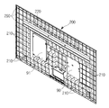
도 1은 본 발명의 일 실시예에 따른 디스플레이 장치의 사시도이고, 도 2는 본 발명의 일 실시예에 따른 디스플레이 장치의 분해사시도이다.FIG. 1 is a perspective view of a display device according to an embodiment of the present invention, and FIG. 2 is an exploded perspective view of a display device according to an embodiment of the present invention.
디스플레이 장치(1) 화상이 표시되는 디스플레이 패널(10)과, 디스플레이 패널(10)과 후방에 배치되어 후방측에서 전달된 광을 전방측에 위치한 디스플레이 패널(10)에 전달되도록 하는 도광판(30)과, 디스플레이 패널(10)과 도광판(30) 사이에 마련되어 도광판(30)에 의해 전달된 광의 광학특성을 개선하기 광학시트(20)를 포함할 수 있다.A
디스플레이 패널(10)은 각각 전극이 마련되어 있는 두 유리기판(미도시) 사이에 액정(미도시)이 봉입되어 형성되는 액정 패널로 이루어질 수 있다.The
광학시트(20)는 도광판(30)을 통해 전달된 광을 다시 확산시키는 확산시트와 확산된 광이 디스플레이 패널(10)에 수직한 방향으로 집광되도록 하는 프리즘 스티와 프리즘 시트를 보호하기 위한 보호 시트 등을 포함할 수 있다.The
또한 디스플레이 장치(1)는 도광판(30)의 일측에 배치되고 도광판(30)에 광을 조사하는 광원을 포함하는 LED기판(50)을 포함할 수 있다. 광원(51, 도3 참고)은 얇은 화면에 의한 박막화가 가능한 점광원으로 발광다이오드(Light Emitting Diode, LED)를 포함할 수 있다. 다만 광원은 LED에 한정되지 않고 발광 가능한 다른 구성일 수 있다.The
광원(51)은 복수로 배치될 수 있으며 LED 기판(50)의 길이 방향을 따라 이격배치될 수 있다.The
본 발명의 일 실시예에 의할 때 LED 기판(50)은 도광판(30)의 일측면에 배치될 수 있다. 이 때 LED 기판(50)의 도광판(30)의 측면의 길이와 대응되는 길이로 연장될 수 있다. 즉, LED 기판(50)은 도광판(30)의 상하 방향 길이와 대응되는 길이로 연장될 수 있다.According to one embodiment of the present invention, the
다만 이에 한정되지 않고 LED 기판(50)은 도광판(30)의 하측 또는 상측에 배치될 수 있다. 이 때 LED기판(50)은 도광판(30)의 좌우 방향 길이와 대응되는 길이로 연장될 수 있다. However, the present invention is not limited thereto and the
또한 본 발명의 일 실시예와 달리 LED 기판(50)은 도광판(30)의 양측에 배치될 수 있다. LED 기판(50)은 도광판(30)의 일측과 타측에 각각 배치되어 도광판(30)의 양측에서 광을 조사할 수 있다.Also, unlike the embodiment of the present invention, the
디스플레이 장치(1)는 LED 기판(50)과 접하고 도광판(30)의 후방에 배치되는 히트 싱크(60)를 포함할 수 있다. 히트 싱크(60)에 대하여는 자세하게 하술한다.The
디스플레이 장치(1)는 도광판(30)의 후측에 배치되고 도광판 후방으로 조사되는 광을 전방으로 반사하는 반사 시트(40)를 포함할 수 있다.The
이하에서는 상술한 각 구성이 탑 섀시(100)와 리어 커버(200)에 의해 지지되는 것에 대해 자세하게 설명한다.Hereinafter, the above-described respective constitutions are supported by the
도 3은 도 1에 표시된 I1-I1선에 따른 측단면도이고, 도 4는 본 발명의 일 실시예에 따른 디스플레이 장치의 탑 섀시에 대한 배면도이고, 도 5는 본 발명의 일 실시예에 의한 디스플레이 장치의 탑 섀시와 일부 구성에 대한 배면도이고, 도 6은 본 발명의 일 실시예에 의한 디스플레이 장치의 탑 섀시와 일부 구성에 대한 배면도이고, 도 7은 본 발명의 일 실시예에 따른 디스플레이 장치의 탑 섀시와 일부 구성에 대한 배면도이다.4 is a rear view of a top chassis of a display device according to an embodiment of the present invention, and FIG. 5 is a cross-sectional view taken along line I1-I1 of FIG. FIG. 6 is a rear view of a top chassis and a partial configuration of a display device according to an embodiment of the present invention, and FIG. 7 is a plan view of a top chassis of a display device according to an embodiment of the present invention Fig. 5 is a rear view of a top chassis and a part of the configuration of the display device. Fig.
종래의 디스플레이 장치에서 상술한 디스플레이 패널, 광학시트, 도광판, LED 기판, 반사 시트와 같은 구성은 탑 섀시와 바텀 섀시로 구성되는 섀시와 미들 몰드에 지지되었다.In the conventional display device, a structure such as the display panel, the optical sheet, the light guide plate, the LED substrate, and the reflection sheet described above was supported on the chassis and the middle mold composed of the top chassis and the bottom chassis.
미들 몰드와 바텀 섀시는 주로 알루미늄 재질로 형성되며, 특히 바텀 섀시의 경우 디스플레이 패널의 면적과 대응되는 크기의 플레이트 형상으로 마련되어 이에 의해 디스플레이 장치의 원가가 상승하는 문제가 발생하였으며, 디스플레이 장치의 외관을 형성하는 커버 내측에 미들 몰드와 바텀 섀시가 마련되어 디스플레이 장치의 두께가 증가하는 문제가 발생하였다.The middle mold and the bottom chassis are mainly made of aluminum, and in particular, in the case of the bottom chassis, the bottom chassis is provided in a plate shape having a size corresponding to the area of the display panel, thereby raising the cost of the display device. A middle mold and a bottom chassis are provided inside the cover to form a thick display device.
이를 해결하기 위하여 본 발명은 미들 몰드와 바텀 섀시를 포함하지 않고, 디스플레이 패널(10), 광학시트(20), 도광판(30), LED 기판(50). 반사 시트(40)의 구성이 탑 섀시(100)와 리어 커버(200)에 지지되게 마련될 수 있다.To solve this problem, the present invention does not include a middle mold and a bottom chassis, but includes a
즉 본 발명의 일 실시예에 따를 때 디스플레이 장치(1)의 섀시는 단일개의 탑 섀시(100)로만 형성될 수 있다. 따라서 탑 섀시(100)를 섀시로 명명할 수 있음은 자명하나 설명의 편의상 탑 섀시(100)로 명명한다.That is, according to an embodiment of the present invention, the chassis of the
도 3 및 도 4에 도시된 바와 같이 디스플레이 패널(10), 광학시트(20), 도광판(30), LED 기판(50). 반사 시트(40)의 구성은 탑 섀시(100)와 리어 커버(200) 사이에 배치될 수 있다. 자세하게는 탑 섀시(100)의 후측면에 디스플레이 패널(10), 광학시트(20), 도광판(30) 및 반사 시트(40)가 순차적으로 배치될 수 있다.The
탑 섀시(100)의 후측면에는 디스플레이 패널(100)이 접하여 지지될 수 있는 제 1지지부(120)가 마련될 수 있다. 제 1지지부(120)는 탑 섀시의 개구의 테두리 측을 따라 마련될 수 있다. 제 1 지지부(120)에 디스플레이 패널(10)의 테두리 측이 접하여 탑 섀시(100)에 지지될 수 있다.A
디스플레이 패널(10)의 후측에 순차적으로 광학시트(20), 도광판(30) 및 반사 시트(40)가 중첩되게 배치될 수 있으며, 도광판(30) 및 반사 시트(40)의 후방에 마련되는 리어 커버(200)의 가압에 의해 디스플레이 패널(10), 광학시트(20), 도광판(30) 및 반사 시트(40)는 탑 섀시(100)에 지지될 수 있다.The
즉, 디스플레이 패널(10), 광학시트(20), 도광판(30), LED 기판(50). 반사 시트(40)가 탑 섀시(100)에 지지되어 있는 상태에서 탑 섀시(100)와 리어 커버(200)가 후크 결합되면서 리어 커버(200)가 탑 섀시(100) 측으로 디스플레이 패널(10), 광학시트(20), 도광판(30), LED 기판(50). 반사 시트(40)를 가압하여 디스플레이 패널(10), 광학시트(20), 도광판(30), LED 기판(50). 반사 시트(40) 구성들이 탑 섀시(100)와 리어 커버(200) 사이에 고정될 수 있다.That is, the
리어 커버(200)는 탑 섀시(100)의 후측에서 탑 섀시(100)와 결합될 수 있다. 자세하게는 탑 섀시(100) 후측면에는 리어 커버(200)가 삽입되는 삽입홈(110)이 마련되고 리어 커버(200)의 전면측의 테두리에 걸쳐 형성되는 삽입부(280)가 삽입홈(110)에 삽입되어 결합될 수 있다.The
삽입홈(110)과 삽입부(280)에는 각각 리어 커버(200)가 탑 섀시(100)에 삽입된 상태에서 후크 결합될 수 있도록 제 1후크부(190)와 제 2후크부(290)가 마련될 수 있다. 삽입부(280)가 삽입홈(110)에 소정부분 삽입되게 되면 제 1후크부(190)와 제 2후크부(290)가 후크 결합되어 탑 섀시(100)와 리어 커버(200)가 고정될 수 있다.The
다만 이에 한정되지 않고 탑 섀시(100)와 리어 커버(200)는 나사 결합 등으로 결합될 수 있고 후크 결합에 한정되지 않는다.However, the present invention is not limited to this, and the
상술한 바와 같이 1차적으로 디스플레이 패널(10)이 탑 섀시(100)의 테두리 측이 제 1지지부(120)에 접하면서 지지되고 도 5에 도시된 바와 같이 디스플레이 패널(10)의 후측에 광학시트(20)가 배치될 수 있다.The edge of the
광학시트(20)는 디스플레이 패널(10)과 도광판(30) 사이에 적층 배치되어 지지됨과 동시에 탑 섀시(100)의 후면에서 돌출되는 걸이부(140)에 걸려 탑 섀시(100)에 의해 고정될 수 있다.The
자세하게는 광학시트(20)의 상측에는 걸이부(140)와 대응되는 크기의 걸이 홀(21)이 마련될 수 있다. 걸이 홀(21)이 걸이부(140)에 걸려서 고정될 수 있다. 본 발명의 일 실시예와 같이 걸이부(140)와 걸이 홀(21)은 두개로 마련될 수 있으며, 이에 한정되지 않고 단일 또는 3개 이상의 복수로 마련될 수 있다.In detail, a
도 6에 도시된 바와 같이 도광판(30)은 광학시트(20) 후방에 배치되어 탑 섀시(100)에 지지될 수 있다. 자세하게는 도광판(30)은 디스플레이 패널(10)과 광학시트(20)와 적층 배치되며, 탑 섀시(100)의 후면에 마련되는 제 2지지부(130)에 접하면서 탑 섀시(100)에 지지될 수 있다.The
제 2지지부(130)는 탑 섀시(100)의 후면 모서리 측에서 후방 측으로 돌출되게 마련될 수 있다. 제 2지지부(130)는 디스플레이 패널(10)과 광학시트(20)의 두께와 대응되는 길이로 돌출될 수 있다.The
도광판(30)이 디스플에이 패널(10)과 광학시트(20)와 적층 배치될 때 디스플레이 패널(10)과 광학시트(20)의 두께에 의해 탑 섀시(100)와 도광판(30) 사이에 발생하는 이격 거리 만큼 제 2지지부(130)가 후방으로 돌출되어 도광판(30)이 탑 섀시(100)에 직접 접하여 지지될 수 있어, 도광판(30)이 안정적으로 지지될 수 있다.The thickness of the
도광판(30)의 후측에는 반사시트(40)가 적층 배치될 수 있다. 반사시트(40)는 광학시트(20)와 같이 걸이부(140)와 대응되는 걸이 홈을 포함할 수 있다.(도 2 참고). 도면에 도시되지는 않았지만 반사시트(40)는 도광판(30)과 리어 커버(200) 사이에 적층 배치됨과 동시에 광학시트(20)와 같이 걸이부(140)에 걸려 탑 섀시(100)에 지지될 수 있다.A
반사시트(40)의 후방에는 히트 싱크(60)가 배치될 수 있다. 히트 싱크(60)는 LED 기판(50)과 접하며 LED 기판(50)과 함께 탑 섀시(50)에 지지될 수 있다. 다만, 이에 한정되지 않고 LED 기판(50)과 히트 싱크(60)는 리어 커버(200) 측에 삽입되거나 리어 커버(200) 측에 결합되는 형식으로 리어 커버(200)에 지지될 수 있다. 히트 싱크(60)에 대하여는 자세하게 후술한다.A
제 1지지부(120)의 일측에는 가림부재(70)가 배치될 수 있다. 자세하게는 LED 기판(50)이 제 1지지부(120)에 접하는 측에 가림부재(70)가 배치될 수 있다.A shielding
가림부재(70)는 광원(51)에서 조사되는 광이 디스플레이 패널(10)과 탑 섀시(100) 사이로 조사되어 도광판(30)을 거치지 않고 직접 외측으로 광이 조사되는 것을 방지하고 LED 기판(50)이 디스플레이 패널(10)과 탑 섀시(100) 사이 공간으로 노출되는 것을 방지하기 위함이다.The shielding
따라서 가림부재(70)는 LED 기판(50)과 탑 섀시(100)의 개구 사이에 배치될 수 있다. 본 발명의 일 실시예에 의할 때 가림부재(70)는 디스플레이 패널(10)의 측면에 배치되어 외부로 LED 기판(50)이 노출되는 것을 방지할 수 있다.Therefore, the shielding
종래의 디스플레이 장치는 미들 몰드에 의해 LED 기판이 외부로 노출되지 않았으나 본 발명은 상술한 바와 같이 디스플레이 장치에 미들 몰드가 포함되지 않아 가림부재(70)에 의해 LED 기판(50)이 외부로 노출되는 것을 방지할 수 있다.In the conventional display device, the LED substrate is not exposed to the outside by the middle mold. However, since the present invention does not include the middle mold in the display device as described above, the
반사시트(40) 및 히트 싱크(60)의 후방에는 상술한 바와 같이 리어 커버(200)가 배치되어 탑 섀시(100)와 후크 결합될 수 있다. 리어 커버(200)는 전방으로 돌출되는 복수의 리브(210)를 포함할 수 있다.(도2 및 도9 참고)The
리어 커버(200)가 탑 섀시(100)와 후크 결합함에 따라 리어 커버(200)에서 돌출되는 복수의 리브(210)는 히트 싱크(60), LED 기판(50), 반사시트(40), 도광판(30), 광학시트(20) 및 디스플레이 패널(10)을 탑 섀시(100) 측으로 가압할 수 있다.A plurality of
따라서 적층 배치되는 디스플레이 패널(10), 광학시트(20), 도광판(30) 및 반사시트(40) 및 LED 기판(50)과 히트 싱크(60)는 전면측으로는 탑 섀시(100), 후면측으로는 리어 커버(200)에 의해 지지되어 고정될 수 있다.Accordingly, the
이하에서는 히트 싱크에 대하여 자세히 설명한다.Hereinafter, the heat sink will be described in detail.
도 7은 본 발명의 일 실시예에 따른 디스플레이 장치의 탑 섀시와 일부 구성에 대한 배면도이고, 도 8은 본 발명의 일 실시예에 따른 디스플레이 장치의 LED기판과 히트 싱크에 대한 사시도이다.FIG. 7 is a rear view of a part of a top chassis of a display device according to an embodiment of the present invention, and FIG. 8 is a perspective view of an LED substrate and a heat sink of a display device according to an embodiment of the present invention.
종래의 디스플레이 장치의 경우 바텀 섀시가 알루미늄 재질로 형성되어 있으며 바텀 섀시가 LED 기판과 접하게 배치되어 있어 LED 기판에서 발생하는 열을 바텀 섀시를 통해 방열할 수 있었다. 따라서 종래의 디스플레이 장치는 바텀 섀시에 의해 별도의 히트 싱크가 배치되지 않았으나, 본 발명의 경우 상술한 바와 같이 바텀 섀시를 포함하지 않기 때문에 LED 기판(50)에서 발생하는 열을 방열하는 구성이 필요할 수 있다. 이에 따라 본 발명의 일 실시예에 의할 때, 디스플레이 장치(1)는 LED 기판(50)과 접하여 LED 기판(50)에서 발생되는 열을 방열시키는 히트 싱크(60)를 포함할 수 있다.In the conventional display device, the bottom chassis is made of aluminum and the bottom chassis is disposed in contact with the LED substrate, so that heat generated from the LED substrate can be dissipated through the bottom chassis. Therefore, the conventional display device does not include a separate heat sink by the bottom chassis. However, since the present invention does not include the bottom chassis as described above, it is necessary to provide a structure for dissipating the heat generated in the
자세하게는 히트 싱크(60)는 도광판(30) 또는 반사 시트(40)와 리어 커버(200) 사이에 배치되는 플레이트 형상으로 마련될 수 있다. 히트 싱크(60)는 방열성이 좋은 알루미늄과 같은 금속 재질을 포함할 수 있다.In detail, the
히트 싱크(60)는LED 기판(50)의 후측 즉, 광원(51)이 실장되는 반대측면과 접하게 배치될 수 있다. 히트 싱크(60)의 일단에는 LED 기판(50)의 후측과 접할 수 있도록 절곡되는 접촉면(61)을 포함할 수 있다. The
접촉면(61)과 LED 기판(50)의 후측면에 접하면서 LED 기판에서 발생되는 열이 접촉면(61)을 통해 전체 히트 싱크(60)로 전달되어 용이하게 방열될 수 있다. 접촉면(61)은 히트 싱크(60)의 플레이트에 대해서 직각으로 절곡될 수 있으며,LED 기판(50)의 후측면의 너비 만큼 연장될 수 있다.The heat generated from the LED substrate while being in contact with the
히트 싱크(60)의 제1변(60a)과 제 2변(60b)을 포함하는 플레이트 형상으로 마련될 수 있다. 제 1변(60a)은 LED 기판(50)의 길이 방향과 대응되는 길이로 형성될 수 있으며, 제 2변(60b)은 제 1변(60a)보다 길이가 짧게 형성될 수 있다.And may be provided in a plate shape including the
제 2변(60b)의 길이가 제 1변(60a)의 길이보다 길어질 경우, 히트 싱크(60)의 넓이가 넓어지게 되어 히트 싱크(60)가 종래의 바텀 섀시의 크기와 유사하게 마련될 수 있는데, 이 경우 히트 싱크(60)를 제작하는 원가가 상승하게 되는 바 문제가 발생할 수 있다.When the length of the
따라서 히트 싱크(60)의 제 1변(60a)은 히트 싱크(60)가 LED 기판(50)가 충분히 접할 수 있도록 LED 기판(50)의 길이와 대응되는 길이로 연장될 수 있으며, 제 2변(60b)은 제 1변(60a)의 길이보다 짧게 형성되어 효과적으로 원가를 절감할 수 있게 할 수 있다.The
같은 맥락으로 히트 싱크(60)는 디스플레이 패널(10) 또는 도광판(30)의 넓이보다 작게 마련될 수 있다. 상술한 바와 같이 히트 싱크(60)의 넓이가 넓어질 경우 디스플레이 장치(1)의 원가가 상승하는 문제가 발생하기 때문이다.In the same manner, the
히트 싱크(60)의 넓이는 바람직하게 도광판(30)의 1/3 크기 이하로 마련될 수 있다. 히트 싱크(60)의 넓이는 본 발명의 일 실시예에 한정되지 않고 LED 기판에서 발생되는 열량에 따라 방열 기능을 충분히 하는 선에서 최소화되는 것이 좋다.The width of the
다만, 후술하겠으나 방열 기능을 향상시키기 위하여 히트 싱크(60)는 리어 커버(200)에 배치되는 보강 부재(220), 또는 보강 부재(220)와 결합 플레이트(91)와 접하게 하여 방열 기능을 향상 시킬 수 있다. However, as will be described later, in order to improve the heat dissipation function, the
이 때 히트 싱크(60)의 넓이가 작아서 방열성이 낮아져도 히트 싱크(60)와 접하는 보강 부재(220), 또는 보강 부재(220와 결합 플레이트(91)와 접하여 부족한 방열성을 높일 수 있다.At this time, even if the heat dissipation is low due to a small width of the
히트 싱크(60)는 상술한 바와 같이 리어 커버(200)의 가압에 의해 반사 시트(40)와 리어 커버(200) 사이에 지지될 수 있으며, 탑 섀시(100)의 후면에서 돌출되는 끼움 돌기(140)와 히트 싱크(60)의 일측에 마련되는 끼움 홈(62)이 각각 끼움 결합되어 히트 싱크(60)가 탑 섀시(100)에 지지될 수 있다.The
자세하게는 끼움 돌기(140)는 제 1지지면(120)에서 후방 측으로 돌출되는 구성이며, 끼움 홈(62)은 끼움 돌기(140)와 대응되는 크기로 마련되어 끼움 홈(62)이 끼움 돌기(140) 측으로 가압되면서 끼움 결합될 수 있다. The
따라서 히트 싱크(60)는 1차적으로 리어 커버(200)의 가압으로 탑 섀시(100)에 지지될 수 있으며, 2차적으로 끼움 돌기(140)와 끼움 홈(62)의 끼움 결합을 통해 탑 섀시(100)에 지지될 수 있다.Accordingly, the
이하에서는 리어 커버(200)와 리어 커버(200)에 결합되는 일부 구성들에 대하여 자세히 설명한다.Hereinafter, some configurations of the
도 9는 본 발명의 일 실시예에 의한 디스플레이 장치의 리어 커버와 일부 구성에 대한 사시도이고, 도 10은 본 발명의 일 실시예에 의한 디스플레이 장치의 리어 커버와 일부 구성에 대한 분해 사시도이고, 도 11은 도 1에 표시된 I2-I2선에 따른 측단면도이다.FIG. 9 is a perspective view of a rear cover and a partial configuration of a display device according to an embodiment of the present invention, FIG. 10 is an exploded perspective view of a rear cover and a partial configuration of a display device according to an embodiment of the present invention, 11 is a side cross-sectional view along the line I2-I2 shown in Fig.
상술한 바와 같이 리어 커버(200)는 탑 섀시(100)에 결합되며 탑 섀시(100)와 리어 커버(200) 사이에 배치되는 구성들을 탑 섀시(100) 측으로 가압하여 미들 몰드나 바텀 섀시 없이도 디스플레이 패널(10), 광학시트(20), 도광판(30) 등의 구성이 내측에서 지지될 수 있도록 할 수 있다.The
리어 커버(200)는 플라스틱 재질을 포함할 수 있다. 이에 따라 리어 커버(200)의 내구성이 약할 수 있는데 이를 보완하기 위하여 보강 부재(220)가 리어 커버(200)에 결합될 수 있다. 또한 복수의 리브(210)가 교차되도록 마련되어 리어 커버(200)의 강성을 높일 수 있다.The
복수의 리브(210)는 리어 커버(200)의 전방을 향해 돌출되게 마련될 수 있다. 복수의 리브(210)는 리어 커버(200) 전방에 배치되는 디스플레이 패널(10), 광학시트(20), 도광판(30) 등의 구성을 탑 섀시(100) 측으로 가압하기 위함이나, 상술한 바와 같이 리어 커버(200)의 강성을 높이는 역할을 할 수 있다.The plurality of
복수의 리브(210)는 도 9에 도시된 바와 같이 교차되어 형성될 수 있지만, 이에 한정되지 않고 다양한 패턴으로 돌출될 수 있다. 복수의 리브(210)의 일단은 반사시트(40), 도광판(30) 또는 히트 싱크(60)가 접할 수 있으며, 리어 커버(200)가 탑 섀시(100)와 후크 결합되면서 복수의 리브(210)가 이에 연동되어 전방으로 가압되고 복수의 리브(210)의 일단이 반사시트(40), 도광판(30) 또는 히트 싱크(60)를 전방으로 가압할 수 있다.The plurality of
보강 부재(220)는 리어 커버(200)의 길이 방향으로 대응되게 연장될 수 있다. 본 발명의 일 실시예에 의할 때는 디스플레이 장치(1)의 좌우 방향으로 연장될 수 있다. 보강 부재(220)는 플라스틱 재질로 형성되는 리어 커버(200) 보다 강성이 강한 금속 재질로 형성될 수 있다. 바람직하게는 히트 싱크(60)과 유사한 알루미늄 재질로 형성될 수 있다. The reinforcing
보강 부재(220)는 리어 커버(200)의 전면 측에 배치될 수 있다. 또한 보강 부재(220)는 도 11에 도시된 바와 같이, 일측이 히트 싱크(60)와 접하게 배치될 수 있다. 히트 싱크(60)와 접하게 배치되어 히트 싱크(60)에서 열을 전달 받아 방열효과를 더 높이기 위함이다.The reinforcing
보강 부재(220)를 통해 히트 싱크(60)의 방열 효과를 증가시킴에 따라 히트 싱크(60)의 크기를 더 줄일 수 있으며, 이에 따라 디스플레이 장치(1)의 원가를 절감하는 효과가 발생할 수 있다.The size of the
리어 커버(200)의 전면측에는 디스플레이 장치(1)를 제어하는 전장품이 실장되는 전장품 기판(90)이 배치될 수 있다. 종래의 디스플레이 장치의 경우 전장품 기판은 알루미늄 재질로 형성되는 바텀 섀시에 배치되도록 구성되어 있으나, 본 발명의 일 실시예에 의할 때 전장품 기판(90)은 리어 커버(200)에 배치될 수 있다.An
전장품 기판(90)의 일측에는 전장품 기판(90)과 접한 상태로 리어 커버(200)와 결합되는 결합 플레이트(91)각 마련될 수 있다. 상술한 바와 같이 전장품 기판이 기존에는 바텀 섀시에 배치되어 바텀 섀시가 전장품 기판에서 발생하는 열을 방열하는 효과가 발생할 수 있었다. 다만 본 발명은 바텀 섀시를 포함하지 않는 바, 추가적으로 결합 플레이트(91)를 포함하여 전장품 기판(90)에서 발생하는 열을 방열할 수 있다. 결합 플레이트(91)는 히트 싱크(60)나 보강 부재(220)와 같은 알루미늄 등과 같은 금속 재질로 마련될 수 있다.A
또한 전장품 기판(90)에 실장된 각종 전장품에서는 유해전파가 발생되는데 특히 유해전파에 의해 형성되는 전자파 방해(EMI: Electromagnetic Interference)가 문제가 될 수 있다. 전자파 방해에 의해 각 전장품 간이나 외부 전자계의 오작동이 발생될 수 있으며, 전자파는 인체에 유해하기 때문에 일정 수준 이하로 전자파 방해가 방생되도록 표준을 두고 있다.In addition, harmful radio waves are generated in various electrical parts mounted on the
종래의 디스플레이 장치의 경우 알루미늄으로 형성되는 바텀 섀시가 전자파의 발생을 차폐하는 역할을 하였는데 본 발명에서는 바텀 섀시가 포함되어 있지 않기 때문에 결합 플레이트(91)가 전장품 기판(90)과 접하게 마련되어 전자파를 차폐하는 역할을 수행할 수 있다.In the case of the conventional display device, the bottom chassis formed of aluminum shields the generation of electromagnetic waves. In the present invention, since the bottom chassis is not included, the
따라서 결합 플레이트(91)는 본 발명의 일 실시예와 같이 플레이트 형상으로 마련될 수 있으나 이에 한정되지 않고 전장품 기판(90)을 감싸는 쉴드캔(shield can) 형태로 마련될 수도 있다.Therefore, the
이하에서는 본 발명의 다른 일 실시예에 의한 리어 커버(200')에 대하여 설명한다. 하술할 리어 커버(200') 이 외의 구성은 도 1 내지 도 11에 개시된 일 실시예에 의한 구성과 동일한 바 그 설명을 생략한다.Hereinafter, a rear cover 200 'according to another embodiment of the present invention will be described. The configuration other than the rear cover 200 'to be described later is the same as the configuration according to the embodiment shown in Figs. 1 to 11, and a description thereof will be omitted.
도 12는 본 발명의 다른 일 실시예에 의한 디스플레이 장치의 리어 커버와 일부 구성에 대한 사시도이고, 도 13은 본 발명의 다른 일 실시예에 의한 디스플레이 장치의 리어 커버의 배면측 사시도이고, 도 14는 본 발명의 다른 일 실시예에 의한 디스플레이 장치의 리어 커버와 일부 구성에 대한 배면측 분해 사시도이다.13 is a rear perspective view of a rear cover of a display device according to another embodiment of the present invention, and FIG. 14 is a perspective view of the rear cover of the display device according to another embodiment of the present invention. Is an exploded rear perspective view of a rear cover and a partial configuration of a display device according to another embodiment of the present invention.
본 발명의 다른 일 실시예에 의할 때, 전장품 기판(90)은 리어 커버(200')의 후측에 배치될 수 있다. 이는 디스플레이 장치(1)의 조립과정에서 조립을 용이하게 하기 위함이다.According to another embodiment of the present invention, the
리어 커버(200')의 후면에는 전장품 기판(90)이 배치될 수 있는 오목한 공간이 마련되고 전장품 기판(90)이 배치된 후 전장품 기판(90)을 커버하여 외부에 전장품 기판(90)이 노출되지 않도록 하기 위해 보조 커버(250)가 마련될 수 있다.A recessed space in which an
리어 커버(200')의 전면측에는 전장품 기판(90)과 결합되는 결합 플레이트(91)가 배치될 수 있다. 이는 상술한 바와 같이 전장품 기판(90)에서 발생되는 열을 방열함과 동시에 전자파를 흡수하기 위함이다.An engaging
자세하게는 전장품 기판(90)은 리어 커버(200') 후측에서 결합 플레이트(91)와 결합될 수 있다. 결합 플레이트(91)는 리어 커버(200')의 후측에 노출되게 배치되어 전장품 기판(90)과 직접 접할 수 있다. 즉 리어 커버(200')에 개구가 형성될 수 있으며 개구에 결합 플레이트(91)가 배치되어 전장품 기판(90)이 리어 커버(200') 후측에서 결합되어도 결합 플레이트(91)와 결합될 수 있다. 전장품 기판(90)은 결합 플레이트(91)에 나사 결합 등을 통해 결합될 수 있다.In detail, the
리어 커버(200')의 개구에 의해 외부로 노출될 수 있는 결합 플레이트(91)와 전장품 기판(90)은 상술한 보고 커버(250)에 의해 커버되어 최종적으로 외부로 노출되지 않을 수 있다.The
이하에서는 본 발명의 다른 일 실시예에 의한 결합 플레이트(91')에 대하여 설명한다. 하술할 결합 플레이트(91') 이 외의 구성은 도 1 내지 도 11에 개시된 일 실시예에 의한 구성과 동일한 바 그 설명을 생략한다.Hereinafter, a coupling plate 91 'according to another embodiment of the present invention will be described. The configuration other than the engaging plate 91 'to be described later is the same as that according to the embodiment disclosed in Figs. 1 to 11, and a description thereof will be omitted.
도 15는 본 발명의 다른 일 실시예에 의한 디스플레이 장치의 리어 커버와 일부 구성에 대한 사시도이고, 도 16은 본 발명의 다른 일 실시예에 의한 디스플레이 장치의 리어 커버와 일부 구성에 대한 분해 사시도이다.FIG. 15 is a perspective view of a rear cover and a partial configuration of a display device according to another embodiment of the present invention, FIG. 16 is an exploded perspective view of a rear cover and a partial configuration of a display device according to another embodiment of the present invention .
결합 플레이트(91')는 전장품 기판(90)과 접하는 동시에 보강 부재(220)와 접하게 배치될 수 있다. 보강 부재(220)와 인접한 결합 플레이트(91')의 일단에는 보강 부재(220)와 접하는 접촉부가 마련될 수 있다.The coupling plate 91 'may be disposed in contact with the
본 발명의 일 실시예에 의할 때 접촉부는 결합 플레이트(91')의 일단에서 절곡되어 보강 부재(220)의 후면과 접하게 배치되고 보강 부재(220)가 리어 커버(200)와 나사 결합 등에 의해 결합될 때 같이 결합될 수 있다.The contact portion is bent at one end of the engaging plate 91 'so as to be in contact with the rear surface of the reinforcing
도 15와 같이 전장품 기판(90)의 개수와 대응하여 전장품 기판(90)에 결합 플레이트(91)가 배치될 수 있다. 본 발명의 다른 일 실시예에 의할 때 전장품 기판(90)이 두개 마련되어 결합 플레이트(91')가 두개 마련되나 이에 한정되지 않고 전장품 기판(90)의 개수에 따라 결합 플레이트(91')가 다수개로 마련될 수 있다.The
결합 플레이트(91')가 보강 부재(220)와 접하게 마련됨에 따라 상술한 것과 같이 보강 부재(220)로 열을 전달하여 방열 효과를 증가시킬 수 있으며, 전자파를 흡수할 수 있는 양을 증가시켜 더 효율적으로 전자파 차폐를 가능하게 할 수 있다.Since the coupling plate 91 'is in contact with the reinforcing
또한 도 11에 개시된 바와 같이 보강 부재(220)는 히트 싱크(60)와도 연결되어 있어 결합 플레이트(91')는 보강 부재(220) 및 히트 싱크(60)와 연결되어 방열 및 전자파 차폐의 효과를 향상 시킬 수 있다.11, the reinforcing
도면에는 도시되지 않았으나 결합 플레이트(91')가 히트 싱크(60)가 배치되는 측까지 연장되게 마련되어 결합 플레이트(91')와 히트 싱크(60)가 직접 연결될 수 있다. 또한 본 발명의 다른 일 실시예와 달리 결합 플레이트(91')와 보강 부재(220) 또는 결합 플레이트(91')와 히트 싱크(60) 사이에 금속재질로 마련되는 연결부재가 마련되어 결합 플레이트(91')와 보강 부재(220) 또는 결합 플레이트(91')와 보강 부재(220) 및 히트 싱크(60)를 서로 연결할 수 있다.Although not shown in the drawing, the coupling plate 91 'is extended to the side where the
본 발명은 상기에서 기재된 실시예들에 한정되는 것은 아니며, 본 발명의 사상에서 벗어나지 않는 범위에서 다양하게 수정 및 변형할 수 있다는 점은 이 기술의 분야에서 통상의 지식을 가진 자에게 자명하다. 따라서 수정예 또는 변형예들은 본 발명의 특허청구범위에 속한다 하여야 할 것이다.It will be apparent to those skilled in the art that various modifications and variations can be made in the present invention without departing from the spirit of the invention. Accordingly, modifications or variations are intended to fall within the scope of the appended claims.
1: 디스플레이 장치 10: 디스플레이 패널
20: 광학시트 30: 도광판
40: 반사시트 50: LED 기판
60: 히트 싱크 70: 가림부재
90: 전장품 기판 91: 결합 플레이트
100: 탑 섀시 110: 삽입 홈
120: 제 1지지면 130: 제 2지지면
140: 끼임 돌기 200: 리어 커버
210: 리브 220: 보강 부재1: Display device 10: Display panel
20: optical sheet 30: light guide plate
40: reflective sheet 50: LED substrate
60: heat sink 70: covering member
90: electrical component substrate 91: coupling plate
100: Top chassis 110: Insert groove
120: first supporting surface 130: second supporting surface
140: Pincer projection 200: Rear cover
210: rib 220: reinforcing member
Claims (20)
상기 디스플레이 패널의 전방에 마련되는 탑 섀시;
상기 디스플레이 패널의 후방에 배치되고 상기 탑 섀시에 지지되는 광학시트;
상기 광학시트 후방에 배치되는 도광판;
상기 도광판의 측면에 배치되어 상기 도광판에 광을 조사하는 LED 기판;
상기 디스플레이 패널의 외관을 형성하고 상기 탑 섀시의 후방에서 상기 탑 섀시에 결합되고 상기 도광판을 상기 탑 섀시측으로 가압하는 리어 커버;
상기 LED기판에서 발생하는 열을 방열하도록 상기 LED기판과 연결되고 상기도광판과 상기 리어 커버 사이에 배치되는 히트 싱크(heat sink);를 포함하는 디스플레이 장치.A display device including a display panel,
A top chassis provided in front of the display panel;
An optical sheet disposed behind the display panel and supported by the top chassis;
A light guide plate disposed behind the optical sheet;
An LED substrate disposed on a side surface of the light guide plate to illuminate the light guide plate;
A rear cover which forms an outer surface of the display panel and is coupled to the tower chassis at the rear of the tower chassis and presses the light guide plate toward the tower chassis;
And a heat sink connected to the LED substrate to dissipate heat generated from the LED substrate and disposed between the light guide plate and the rear cover.
상기 리어 커버는 플라스틱 재질을 포함하는 디스플레이 장치.The method according to claim 1,
Wherein the rear cover comprises a plastic material.
상기 히트 싱크는 상기 LED기판의 길이 방향과 대응되는 방향으로 연장되는 제 1변과 상기 제 1변보다 길이가 짧은 제 2변을 포함하는 플레이트 형상으로 마련되는 디스플레이 장치.The method according to claim 1,
Wherein the heat sink is provided in a plate shape including a first side extending in a direction corresponding to a longitudinal direction of the LED substrate and a second side having a length shorter than the first side.
상기 히트 싱크의 넓이는 상기 도광판의 넓이보다 작은 디스플레이 장치.3. The method of claim 2,
And the width of the heat sink is smaller than the width of the light guide plate.
상기 리어 커버의 강성을 보강하도록 상기 리어 커버와 결합되는 보강부재를 더 포함하고, 상기 보강부재의 적어도 일측은 상기 히트 싱크와 접하는 디스플레이 장치.The method according to claim 1,
Further comprising a reinforcing member coupled to the rear cover to reinforce the rigidity of the rear cover, wherein at least one side of the reinforcing member contacts the heat sink.
상기 리어 커버는 상기 탑 섀시 측으로 돌출되고 상기 도광판이 상기 탑 섀시에 지지되도록 상기 도광판을 상기 탑 섀시 측으로 가압하는 복수의 리브를 포함하는 디스플레이 장치.The method according to claim 1,
And the rear cover includes a plurality of ribs projecting toward the tower chassis and pressing the light guide plate toward the tower chassis so that the light guide plate is supported by the tower chassis.
상기 탑 섀시는 상기 광학시트가 걸리도록 상기 광학시트 측으로 돌출되는 걸이부를 포함하고,
상기 광학시트는 상기 걸이부가 관통되도록 마련되는 걸이홀을 포함하는 디스플레이 장치.The method according to claim 1,
Wherein the top chassis includes a hook portion protruding toward the optical sheet so as to catch the optical sheet,
Wherein the optical sheet includes a hook hole provided to allow the hook portion to pass therethrough.
상기 도광판 후방에 배치되는 반사시트를 더 포함하고,
상기 반사시트는 상기 걸이부에 걸려 상기 탑 섀시에 지지되는 디스플레이 장치.8. The method of claim 7,
And a reflective sheet disposed behind the light guide plate,
Wherein the reflective sheet is held by the hook portion and supported by the top chassis.
상기 탑 섀시는 상기 도광판이 지지되도록 상기 도광판 측으로 돌출되는 도광판 지지부를 포함하고, 상기 도광판 지지부는 상기 디스플레이 패널과 상기 광학패널의 두께의 합과 대응되는 길이로 돌출되는 디스플레이 장치.The method according to claim 1,
Wherein the top chassis includes a light guide plate support portion protruding toward the light guide plate to support the light guide plate, and the light guide plate support portion protrudes with a length corresponding to a sum of thicknesses of the display panel and the optical panel.
상기 탑 섀시는 상기 히트 싱크가 지지되도록 상기 히트 싱크 측으로 돌출되는 끼움 돌기를 포함하고, 상기 히트 싱크는 상기 끼움 돌기와 끼움 결합되도록 마련되는 끼움홈을 포함하는 디스플레이 장치.The method according to claim 1,
Wherein the top chassis includes a fitting protrusion protruded toward the heat sink so as to support the heat sink, and the heat sink includes a fitting groove fitted to the fitting protrusion.
전장품이 실장되는 전장품 기판을 더 포함하고,
상기 전장품 기판은 상기 리어 커버에 결합되는 디스플레이 장치.The method according to claim 1,
Further comprising an electrical component substrate on which an electrical component is mounted,
And the electric component substrate is coupled to the rear cover.
상기 전장품 기판의 일측에는 상기 전장품 기판의 넓이와 대응되는 넓이로 마련되는 결합 플레이트가 배치되는 디스플레이 장치.12. The method of claim 11,
And a coupling plate provided on one side of the electric component substrate, the coupling plate having a width corresponding to the width of the electrical component substrate.
상기 전장품 기판은 상기 도광판과 상기 리어 커버 사이에 배치되는 디스플레이 장치.12. The method of claim 11,
And the electric component substrate is disposed between the light guide plate and the rear cover.
상기 전장품 기판은 상기 리어 커버의 후방에 배치되고,
상기 리어커버는 상기 전장품 기판을 커버하는 보조 커버를 포함하는 디스플레이 장치.12. The method of claim 11,
Wherein the electric component substrate is disposed behind the rear cover,
And the rear cover includes an auxiliary cover covering the electrical component substrate.
상기 결합플레이트는 상기 히트 싱크와 연결되는 디스플레이 장치13. The method of claim 12,
Wherein the coupling plate is connected to the heat sink,
상기 디스플레이 패널의 전방에 마련되는 탑 섀시;
상기 디스플레이 패널의 후방에 마련되고 상기 탑 섀시와 결합하는 리어 커버;
상기 탑 섀시와 상기 리어 커버 사이에 배치되어 지지되는 광학시트와 도광판;
상기 도광판에 광을 조사하도록 상기 도광판의 측방에 배치되는 LED 기판;
상기 LED기판에서 발생하는 열을 방열하도록 상기 LED기판과 연결되는 히트 싱크(heat sink);
상기 리어 커버의 강성을 보강하도록 상기 리어 커버와 결합되고 상기 히트 싱크와 연결되는 보강 부재;를 포함하는 디스플레이 장치.A display panel;
A top chassis provided in front of the display panel;
A rear cover provided at the rear of the display panel and engaged with the top chassis;
An optical sheet supported and disposed between the top chassis and the rear cover, and a light guide plate;
An LED substrate disposed on a side of the light guide plate to emit light to the light guide plate;
A heat sink connected to the LED substrate to dissipate heat generated from the LED substrate;
And a reinforcing member coupled to the rear cover to reinforce the rigidity of the rear cover and connected to the heat sink.
상기 리어 커버에 결합되고 전장품이 실장되는 전장품 기판을 더 포함하고,
상기 전장품 기판의 일측에는 상기 전장품 기판에서 발생하는 전자파를 감소시키는 결합 플레이트가 배치되는 디스플레이 장치.17. The method of claim 16,
Further comprising an electrical component board coupled to the rear cover and having an electrical component mounted thereon,
And a coupling plate for reducing electromagnetic waves generated from the electrical component substrate is disposed on one side of the electrical component substrate.
상기 결합 플레이트는 상기 히트 싱크와 상기 보강 부재 중 적어도 하나와 연결되는 디스플레이 장치.18. The method of claim 17,
Wherein the coupling plate is connected to at least one of the heat sink and the reinforcing member.
상기 탑 섀시와 상기 리어 커버는 후크 결합되는 디스플레이 장치.17. The method of claim 16,
Wherein the top chassis and the rear cover are hook-coupled.
상기 디스플레이 패널의 전방에 마련되는 섀시;
상기 디스플레이 패널의 외관을 형성하고 상기 디스플레이 패널의 후방에서 상기 섀시와 결합하고 플라스틱 재질을 포함하는 리어 커버;
상기 섀시와 상기 리어 커버에 의해 지지되는 도광판;
상기 도광판에 광을 조사하는 LED기판;
상기 LED기판과 연결되고 상기 디스플레이 패널과 상기 리어 커버 사이에 배치되는 금속 재질을 포함하는 플레이트;를 포함하는 디스플레이 장치.A display device including a display panel,
A chassis provided in front of the display panel;
A rear cover which forms an outer appearance of the display panel and is joined to the chassis at the rear of the display panel and includes a plastic material;
A light guide plate supported by the chassis and the rear cover;
An LED substrate for emitting light to the light guide plate;
And a plate connected to the LED substrate and including a metal material disposed between the display panel and the rear cover.
Priority Applications (5)
| Application Number | Priority Date | Filing Date | Title |
|---|---|---|---|
| KR1020160052881A KR102600981B1 (en) | 2016-04-29 | 2016-04-29 | Display apparatus |
| EP17789794.9A EP3380888B1 (en) | 2016-04-29 | 2017-03-28 | Display apparatus |
| CN201780013447.4A CN108700763B (en) | 2016-04-29 | 2017-03-28 | Display device |
| PCT/KR2017/003329 WO2017188609A1 (en) | 2016-04-29 | 2017-03-28 | Display apparatus |
| US15/478,319 US10473960B2 (en) | 2016-04-29 | 2017-04-04 | Display apparatus |
Applications Claiming Priority (1)
| Application Number | Priority Date | Filing Date | Title |
|---|---|---|---|
| KR1020160052881A KR102600981B1 (en) | 2016-04-29 | 2016-04-29 | Display apparatus |
Publications (2)
| Publication Number | Publication Date |
|---|---|
| KR20170123820A true KR20170123820A (en) | 2017-11-09 |
| KR102600981B1 KR102600981B1 (en) | 2023-11-13 |
Family
ID=60157902
Family Applications (1)
| Application Number | Title | Priority Date | Filing Date |
|---|---|---|---|
| KR1020160052881A KR102600981B1 (en) | 2016-04-29 | 2016-04-29 | Display apparatus |
Country Status (5)
| Country | Link |
|---|---|
| US (1) | US10473960B2 (en) |
| EP (1) | EP3380888B1 (en) |
| KR (1) | KR102600981B1 (en) |
| CN (1) | CN108700763B (en) |
| WO (1) | WO2017188609A1 (en) |
Cited By (1)
| Publication number | Priority date | Publication date | Assignee | Title |
|---|---|---|---|---|
| WO2021162142A1 (en) * | 2020-02-13 | 2021-08-19 | 엘지전자 주식회사 | Display device |
Families Citing this family (6)
| Publication number | Priority date | Publication date | Assignee | Title |
|---|---|---|---|---|
| CN107526391B (en) * | 2016-06-21 | 2020-05-08 | 鸿富锦精密电子(重庆)有限公司 | Display device |
| EP3690523B1 (en) * | 2017-09-26 | 2023-05-03 | LG Electronics Inc. | Display device |
| CN109491140B (en) * | 2018-11-30 | 2021-06-08 | 海信视像科技股份有限公司 | Display device |
| KR20200138461A (en) * | 2019-05-29 | 2020-12-10 | 삼성디스플레이 주식회사 | Display device, method of manufacturing display device, and guide structure used therein |
| CN112150939A (en) * | 2019-06-28 | 2020-12-29 | 株式会社午星显示 | OLED display device and manufacturing method of rear cover thereof |
| US11428970B2 (en) * | 2020-05-29 | 2022-08-30 | Dell Products L.P. | Display device having a uni-body integrated housing |
Citations (6)
| Publication number | Priority date | Publication date | Assignee | Title |
|---|---|---|---|---|
| KR20070076520A (en) * | 2006-01-18 | 2007-07-24 | 미쓰비시덴키 가부시키가이샤 | Planar light source unit and image display apparatus using the same |
| KR20120076179A (en) * | 2010-12-29 | 2012-07-09 | 엘지디스플레이 주식회사 | Liquid crystal display device having light emitting diode backlight |
| KR20140104769A (en) * | 2013-02-21 | 2014-08-29 | 엘지전자 주식회사 | Display device |
| US20150049255A1 (en) * | 2012-05-29 | 2015-02-19 | Sharp Kabushiki Kaisha | Display device and television device |
| US20150131026A1 (en) * | 2013-11-11 | 2015-05-14 | Young Lighting Technology Inc. | Flat panel display |
| KR20150112418A (en) * | 2014-03-28 | 2015-10-07 | 엘지전자 주식회사 | Display apparatus |
Family Cites Families (32)
| Publication number | Priority date | Publication date | Assignee | Title |
|---|---|---|---|---|
| US5422751A (en) * | 1992-10-14 | 1995-06-06 | Apple Computer, Inc. | Liquid crystal display assembly employing front bezel, frame holding liquid crystal cell attached to bezel, and light source and back plate attached to bezel |
| KR100269943B1 (en) | 1997-03-03 | 2000-10-16 | 윤종용 | Display module formed as a single body |
| JP2000235183A (en) * | 1999-02-16 | 2000-08-29 | Matsushita Electric Ind Co Ltd | Illuminator and portable information equipment provided with the same |
| KR100619582B1 (en) * | 1999-10-08 | 2006-09-01 | 삼성전자주식회사 | Liquid crystal display module, liquid crystal display device contain the liquid crystal display module and method for assembling the same |
| KR101006444B1 (en) | 2003-12-24 | 2011-01-06 | 삼성전자주식회사 | Liquid crystal display device provided with divided top chassis having improved connecting members |
| JP3108915U (en) * | 2004-11-22 | 2005-04-28 | 船井電機株式会社 | Liquid crystal television and liquid crystal display device |
| KR101082436B1 (en) * | 2005-01-19 | 2011-11-11 | 삼성에스디아이 주식회사 | Plasma display apparatus |
| JP4482473B2 (en) * | 2005-03-25 | 2010-06-16 | シャープ株式会社 | Liquid crystal display |
| KR101189088B1 (en) * | 2005-06-22 | 2012-11-09 | 삼성디스플레이 주식회사 | Back light assembly and liquid crystal display apparatus having the same |
| JP2009098310A (en) * | 2007-10-15 | 2009-05-07 | Hitachi Displays Ltd | Liquid crystal display device |
| KR101340603B1 (en) * | 2007-11-15 | 2013-12-11 | 엘지디스플레이 주식회사 | Liquid Crystal Display Device Module |
| CN101441359B (en) * | 2007-11-19 | 2011-06-08 | 鸿富锦精密工业(深圳)有限公司 | Frame and backlight module unit using the same |
| KR20100106790A (en) * | 2009-03-24 | 2010-10-04 | 삼성전자주식회사 | Display device |
| TW201101826A (en) * | 2009-06-22 | 2011-01-01 | Hannspree Inc | Display housing capable of collocating liquid crystal panel module with multiple of sizes |
| JP5317365B2 (en) * | 2010-01-07 | 2013-10-16 | エルジー イノテック カンパニー リミテッド | Backlight unit |
| KR101054768B1 (en) * | 2010-06-11 | 2011-08-05 | 엘지이노텍 주식회사 | A backlight unit and a display device |
| US8970793B2 (en) * | 2011-08-30 | 2015-03-03 | Funai Electric Co., Ltd. | Display device, and television device |
| WO2013047366A1 (en) * | 2011-09-30 | 2013-04-04 | シャープ株式会社 | Display apparatus and television receiver |
| KR20130040661A (en) * | 2011-10-14 | 2013-04-24 | 삼성전자주식회사 | Back light unit and display device having the same |
| CN102506391A (en) * | 2011-10-20 | 2012-06-20 | 深圳市华星光电技术有限公司 | Backboard, backlight module and method for locking reinforcement bar on backboard |
| US9621838B2 (en) * | 2011-10-25 | 2017-04-11 | Funai Electric Co., Ltd. | Display device and television apparatus |
| WO2013077243A1 (en) * | 2011-11-22 | 2013-05-30 | シャープ株式会社 | Illumination device, display device and television receiver |
| WO2013103120A1 (en) * | 2012-01-06 | 2013-07-11 | シャープ株式会社 | Display device and television receiver |
| US20130215356A1 (en) * | 2012-02-16 | 2013-08-22 | Yajun Yu | Connecting Piece for Backlight Module, Backlight Module and LCD Device |
| WO2013176399A1 (en) * | 2012-05-25 | 2013-11-28 | Samsung Electronics Co., Ltd. | Liquid crystal display apparatus |
| WO2013191050A1 (en) * | 2012-06-19 | 2013-12-27 | シャープ株式会社 | Display device and television receiver |
| CN104769353B (en) * | 2012-11-08 | 2018-06-12 | 夏普株式会社 | Back lighting device and liquid crystal display device |
| JP5955753B2 (en) * | 2012-11-30 | 2016-07-20 | 船井電機株式会社 | Display device |
| TWI493259B (en) * | 2013-04-01 | 2015-07-21 | Au Optronics Corp | Light source apparatus |
| KR20150026056A (en) | 2013-08-30 | 2015-03-11 | 삼성전자주식회사 | An electronic device with curved bottom and operating method thereof |
| CN103925531B (en) * | 2014-05-08 | 2017-01-04 | 青岛海信电器股份有限公司 | A kind of backlight module and liquid crystal indicator |
| CN104006331A (en) * | 2014-05-12 | 2014-08-27 | 深圳市华星光电技术有限公司 | Backlight module and liquid crystal display device |
-
2016
- 2016-04-29 KR KR1020160052881A patent/KR102600981B1/en active IP Right Grant
-
2017
- 2017-03-28 WO PCT/KR2017/003329 patent/WO2017188609A1/en active Application Filing
- 2017-03-28 EP EP17789794.9A patent/EP3380888B1/en active Active
- 2017-03-28 CN CN201780013447.4A patent/CN108700763B/en active Active
- 2017-04-04 US US15/478,319 patent/US10473960B2/en not_active Expired - Fee Related
Patent Citations (6)
| Publication number | Priority date | Publication date | Assignee | Title |
|---|---|---|---|---|
| KR20070076520A (en) * | 2006-01-18 | 2007-07-24 | 미쓰비시덴키 가부시키가이샤 | Planar light source unit and image display apparatus using the same |
| KR20120076179A (en) * | 2010-12-29 | 2012-07-09 | 엘지디스플레이 주식회사 | Liquid crystal display device having light emitting diode backlight |
| US20150049255A1 (en) * | 2012-05-29 | 2015-02-19 | Sharp Kabushiki Kaisha | Display device and television device |
| KR20140104769A (en) * | 2013-02-21 | 2014-08-29 | 엘지전자 주식회사 | Display device |
| US20150131026A1 (en) * | 2013-11-11 | 2015-05-14 | Young Lighting Technology Inc. | Flat panel display |
| KR20150112418A (en) * | 2014-03-28 | 2015-10-07 | 엘지전자 주식회사 | Display apparatus |
Cited By (1)
| Publication number | Priority date | Publication date | Assignee | Title |
|---|---|---|---|---|
| WO2021162142A1 (en) * | 2020-02-13 | 2021-08-19 | 엘지전자 주식회사 | Display device |
Also Published As
| Publication number | Publication date |
|---|---|
| US10473960B2 (en) | 2019-11-12 |
| CN108700763A (en) | 2018-10-23 |
| CN108700763B (en) | 2022-02-08 |
| KR102600981B1 (en) | 2023-11-13 |
| US20170315400A1 (en) | 2017-11-02 |
| WO2017188609A1 (en) | 2017-11-02 |
| EP3380888B1 (en) | 2021-01-13 |
| EP3380888A4 (en) | 2019-01-09 |
| EP3380888A1 (en) | 2018-10-03 |
Similar Documents
| Publication | Publication Date | Title |
|---|---|---|
| KR20170123820A (en) | Display apparatus | |
| KR102119532B1 (en) | Display apparatus | |
| US10304359B2 (en) | Display device | |
| US20120257136A1 (en) | Display and Display Module | |
| US20140286053A1 (en) | Display device, electronic apparatus and illumination device | |
| JP5857496B2 (en) | LIGHTING DEVICE, DISPLAY DEVICE, AND ELECTRONIC DEVICE | |
| US20150055053A1 (en) | Display device and support member thereof | |
| WO2015002017A1 (en) | Illumination device, display device, and television receiving device | |
| US20140247398A1 (en) | Display | |
| KR102367068B1 (en) | Display apparatus | |
| JP5519758B2 (en) | Liquid crystal display | |
| KR20140036715A (en) | Display module of display device | |
| JP4212062B1 (en) | LCD panel | |
| US10120237B2 (en) | Display apparatus | |
| US9877403B2 (en) | Display device | |
| JP5367867B2 (en) | Liquid crystal display device and television receiver | |
| JP2018040853A (en) | Display and television receiver | |
| WO2012169440A1 (en) | Lighting device, display device and television receiver | |
| KR102186464B1 (en) | Display module and display apparatus having the same | |
| JP6333905B2 (en) | Display device and television receiver | |
| WO2013088776A1 (en) | Display device and television receiver | |
| JP6333906B2 (en) | Display device and television receiver | |
| JP2014059955A (en) | Lighting device and display device including the same | |
| KR101726635B1 (en) | Liquid Crystal Display Device | |
| WO2013065392A1 (en) | Illumination device, display device, and television receiving device |
Legal Events
| Date | Code | Title | Description |
|---|---|---|---|
| E902 | Notification of reason for refusal | ||
| E902 | Notification of reason for refusal | ||
| E701 | Decision to grant or registration of patent right | ||
| GRNT | Written decision to grant |