KR20170120558A - Electrical generator system - Google Patents
Electrical generator system Download PDFInfo
- Publication number
- KR20170120558A KR20170120558A KR1020177016357A KR20177016357A KR20170120558A KR 20170120558 A KR20170120558 A KR 20170120558A KR 1020177016357 A KR1020177016357 A KR 1020177016357A KR 20177016357 A KR20177016357 A KR 20177016357A KR 20170120558 A KR20170120558 A KR 20170120558A
- Authority
- KR
- South Korea
- Prior art keywords
- generator system
- zinc oxide
- metal
- radionuclide
- layer
- Prior art date
Links
Images


Classifications
-
- G—PHYSICS
- G21—NUCLEAR PHYSICS; NUCLEAR ENGINEERING
- G21H—OBTAINING ENERGY FROM RADIOACTIVE SOURCES; APPLICATIONS OF RADIATION FROM RADIOACTIVE SOURCES, NOT OTHERWISE PROVIDED FOR; UTILISING COSMIC RADIATION
- G21H1/00—Arrangements for obtaining electrical energy from radioactive sources, e.g. from radioactive isotopes, nuclear or atomic batteries
- G21H1/06—Cells wherein radiation is applied to the junction of different semiconductor materials
-
- G—PHYSICS
- G21—NUCLEAR PHYSICS; NUCLEAR ENGINEERING
- G21H—OBTAINING ENERGY FROM RADIOACTIVE SOURCES; APPLICATIONS OF RADIATION FROM RADIOACTIVE SOURCES, NOT OTHERWISE PROVIDED FOR; UTILISING COSMIC RADIATION
- G21H1/00—Arrangements for obtaining electrical energy from radioactive sources, e.g. from radioactive isotopes, nuclear or atomic batteries
- G21H1/02—Cells charged directly by beta radiation
-
- G—PHYSICS
- G21—NUCLEAR PHYSICS; NUCLEAR ENGINEERING
- G21H—OBTAINING ENERGY FROM RADIOACTIVE SOURCES; APPLICATIONS OF RADIATION FROM RADIOACTIVE SOURCES, NOT OTHERWISE PROVIDED FOR; UTILISING COSMIC RADIATION
- G21H1/00—Arrangements for obtaining electrical energy from radioactive sources, e.g. from radioactive isotopes, nuclear or atomic batteries
- G21H1/04—Cells using secondary emission induced by alpha radiation, beta radiation, or gamma radiation
Abstract
방사성 물질로부터의 에너지를 사용하는 전력 전지. 장치는 ZnO를 반도체로 사용하며 금속-반도체 접합에서 에너지가 발생된다. ZnO는 박층으로 배열된다. 이는 우수한 내구성과 비교적 높은 전력 생산을 허용한다.Power cells using energy from radioactive materials. The device uses ZnO as a semiconductor and generates energy at the metal-semiconductor junction. ZnO is arranged in a thin layer. This allows excellent durability and relatively high power production.
Description
본 발명은 발전 분야에 관한 것으로, 특히 방사능 방출의 에너지로부터 변환된 전기 에너지에 관한 것이다. Field of the Invention The present invention relates to the field of power generation, and more particularly to electrical energy converted from energy of radiation emission.
전력 셀은 외부 부하를 구동하기 위한 자체 전기 에너지원을 제공한다. 전력 셀의 일반적인 예는 전기화학 전지이다. 전기화학 전지는 상대적으로 저렴한 비용으로 일정 시간 전력 수요를 제공하는 데 효과적이지만, 제한 요소는 물질 유형에 의해 한정되는 사용 가능한 에너지 및 중량이다. 제한된 에너지 저장용량 및, 질량에 대한 전기화학 전지의 에너지 밀도로 인해, 대체 전력 셀을 생산하기 위한 다양한 시도가 있어 왔으며, 예컨대 더 높은 이론적 에너지 밀도의 한계로 인하여 방사성 동위원소에 의해 구동되는 전지와 같은 것이다.The power cell provides its own source of electrical energy to drive the external load. A typical example of a power cell is an electrochemical cell. Although electrochemical cells are effective at providing relatively constant low-cost, constant-time power demand, the limiting factor is available energy and weight, which is defined by the material type. Due to the limited energy storage capacity and the energy density of the electrochemical cell with respect to mass, various attempts have been made to produce alternative power cells, for example due to the higher theoretical energy density limitations, It is the same.
방사성 동위원소-구동 전지에는 여러 상이한 유형이 있다. 그러한 유형 중 하나는 전기 에너지를 생산하기 위해 방사성 물질의 붕괴 동안 생성되는 열을 사용하는 방사성 열 발생기(RTG: radio thermal generator)이다. 이들 장치는 열 에너지가 전기 에너지로 변환되는 효율이 낮다. 따라서 RTG는 전원을 제조하기 위하여 일반적으로 매우 높은 에너지의 방사성 동위원소와 함께 사용되며 일반적으로 실질적인 차폐가 필요하다. 또한 전력 출력이 낮다.There are many different types of radioisotope-driven cells. One such type is a radio thermal generator (RTG) that uses heat generated during the collapse of radioactive materials to produce electrical energy. These devices are less efficient at converting thermal energy into electrical energy. Thus, RTGs are typically used with very high energy radioactive isotopes to produce power supplies and generally require substantial shielding. Also, the power output is low.
다른 유형의 방사성 동위원소-구동 전지는 방사성 동위원소, 발광 물질 및 광전지를 사용하는 간접 변환 장치이다. 방사성 동위원소에 의해 방출된 붕괴 입자는 발광 물질을 여기시킨다. 발광 물질에 의해 방출된 광은 광전지에 의해 흡수되어 전기를 발생시킨다. 이 유형의 전지는 2단계 변환으로 인해 효율이 낮고 발광 물질이 방출로 인해 손상되기 때문에 상대적으로 수명이 짧다.Other types of radioisotope-driven cells are indirect transducers using radioactive isotopes, luminescent materials and photovoltaic cells. The collapsed particles emitted by the radioisotope excite the luminescent material. The light emitted by the light emitting material is absorbed by the photocell to generate electricity. This type of cell has a relatively short life due to the low efficiency due to the two-step conversion and damage to the emissive material due to emission.
방사성 동위원소 구동 전지의 다른 예는 방사성 동위원소 및 반도체 물질을 사용하는 직접 변환 장치이다. 종래의 반도체는 방사성 동위원소 붕괴 생성물로부터 부수적인 방사선 손상을 겪기 때문에 이 응용에서는 사용이 제한적이다. 특히, 입사되는 고 에너지 베타 입자가 생성된 전하 캐리어를 산란시키고 끌어들이는(trap) 결함을 반도체 내에 발생시킨다. 손상은 축적되며 따라서 시간이 지남에 따라 전지 성능이 저하된다.Another example of a radioisotope-driven cell is a direct conversion device using radioactive isotopes and semiconductor materials. Conventional semiconductors suffer from secondary radiation damage from radioisotope decay products and are therefore of limited use in this application. Particularly, the high energy beta particles generated cause scattering of the generated charge carriers and trap defects in the semiconductor. Damage accumulates and battery performance deteriorates over time.
미국 특허 제5,260,621호는 열 발생을 수반하는 상대적으로 고 에너지의 방사선원 및, 방사성 동위원소에 반응하는 결함 생성을 특징으로 하는 AlGaAs와 같은 벌크 결정성 반도체를 포함하는 고체 상태 핵 전지를 개시한다. 물질은 방사선 손상이 전지의 높은 작동 온도에서 어닐링에 의해 보수되도록 선택된다. 이 장치는 낮은 효율로 인하여 고 에너지 방사선원의 사용이 필요하며 또한 기능하기 위해 높은 작동 온도가 필요하다.U. S. Patent No. 5,260, 621 discloses a solid state nuclear cell comprising a relatively high energy radiation source with heat generation and a bulk crystalline semiconductor such as AlGaAs characterized by defect generation responsive to radioisotopes. The material is selected so that radiation damage is repaired by annealing at high operating temperatures of the cell. This device requires the use of high energy radiation sources due to its low efficiency and also requires high operating temperatures to function.
미국 특허 제5859484호는 GaInAsP와 같은 결정성 반도체 물질 기판을 포함하는 고체 상태 방사성 동위원소-구동 반도체 전지를 교시한다. 이 전지는 바람직하게는 수명을 최대화하기 위해 반도체 물질의 열화를 최소화하고자 저 에너지 입자만을 방출하는 방사성 동위원소를 사용한다. 저 에너지 방사선원을 사용하는 것의 결과는 더 낮은 최대 전력 출력이다.US 5859484 teaches a solid state radioisotope-driven semiconductor cell comprising a crystalline semiconductor material substrate such as GaInAsP. The cell preferably uses a radioactive isotope that emits low energy particles only to minimize deterioration of the semiconductor material to maximize its lifetime. The result of using a low energy radiation source is a lower maximum power output.
이러한 다른 장치는 미국 특허 제6479919호에 개시되어 있으며, 20면체 붕화물, 예를 들면 B12P2 또는 B12As2, 베타 방사선원 및 전기 에너지를 외부 부하로 전달하기 위한 수단을 포함하는 베타 셀을 기술하고 있다. 비화 붕소 및 인화 붕소의 제조에는 비용이 많이 들며, 이는 이들 유형의 장치를 생산하는 비용을 증가시킨다. 또한, 이러한 장치의 생산은 비화물 및 인화물 취급과 연관된 건강, 안전 및 환경 위험을 증가시켰다.Such other devices are disclosed in U.S. Patent No. 6479919, and include a beta-cell including a bicontinuous boron, such as B 12 P 2 or B 12 As 2 , a beta radiation source and means for delivering electrical energy to an external load . The production of boron boron and boron phosphide is costly, which increases the cost of producing these types of devices. In addition, the production of such devices has increased health, safety and environmental hazards associated with non-cargo and phosphates handling.
요약하면, 현재 이용 가능한 방사성 동위원소 구동 셀의 문제점은 방출된 에너지를 전기 에너지로 변환하는 비효율, 장치 물질에 영향을 주는 방사선 손상, 고 에너지 핵원 및 열화될 수있는 반도체 물질에 대한 차폐 요건을 포함한다.In summary, the problems with currently available radioisotope driving cells include inefficiencies in converting emitted energy into electrical energy, radiation damage affecting device materials, high energy sources and shielding requirements for degradable semiconductor materials do.
본 발명의 목적은 내구성과 전력 출력 사이의 개선된 균형을 나타내는 방사성 동위원소 구동 셀을 제공하는 것이다.It is an object of the present invention to provide a radioisotope driving cell that exhibits an improved balance between durability and power output.
본 발명에 따르면 방사성 핵종 물질; 산화아연 박층; 산화아연과 접촉하고 그 사이에 금속-반도체 접합을 형성하는 금속 전극--방사성 핵종 물질로부터 리시브된(received) 방사능 방출이 금속-반도체 접합에서 전기 에너지로 변환됨--; 및 전극에 연결되며, 부하에 연결될 때 상기 전기 에너지의 흐름을 용이하게 하는 전기 접점을 포함하는 발전기 시스템이 제공된다.According to the present invention, a radionuclide material; Zinc oxide thin layer; A metal electrode in contact with the zinc oxide and forming a metal-semiconductor junction therebetween; a radioactive radiation received from the radionuclide material is converted from the metal-semiconductor junction to electrical energy; And an electrical contact connected to the electrode and facilitating the flow of electrical energy when connected to the load.
산화아연의 사용이 놀라운 결과를 갖는 것이 발명자에 의해 발견되었다. 산화아연이 고유한 n형 반도체이지만, 안정적으로 도핑된 p형 ZnO 물질이 없기 때문에 반도체 물질로서는 상업적인 응용이 없거나 제한되었다. 결과적으로, 방사성 동위원소 구동 셀을 구성하는 일차적인 방향인 p-n 접합을 형성하기 위한 반도체 물질로는 부적절한 선택으로 간주되었다.It has been discovered by the inventors that the use of zinc oxide has surprising results. Although zinc oxide is a unique n-type semiconductor, there is no commercially applicable or limited application as a semiconductor material because there is no stably doped p-type ZnO material. As a result, the semiconductor material for forming the p-n junction, which is the primary direction of constituting the radioisotope driving cell, has been regarded as an inappropriate choice.
전통적으로 받아들여지는 반도체 물질의 선택, 예컨대 GaAs, GaInAs; 또는 Si, Si-C; 또는 CdTe 등은 고 준위의 방사선에 노출될 때 구조적으로 열화되는 것으로 밝혀졌다.Selection of traditionally accepted semiconductor materials, such as GaAs, GaInAs; Or Si, Si-C; Or CdTe have been found to be structurally degraded when exposed to high levels of radiation.
발명자는 산화아연이 적절한 두께로 사용될 때 고 방사선 준위를 견딜 수 있으며, 금속-반도체 접합의 일부로 사용될 때 (p-n 접합과 반대로) 양호한 전기 발생 출력을 나타내는 것을 발견하였다. The inventors have found that zinc oxide can withstand high radiation levels when used at an appropriate thickness and exhibits a good electricity generating output (as opposed to a p-n junction) when used as a part of a metal-semiconductor junction.
본 발명의 실시예가 이제 첨부 도면을 참조하여 설명된다.
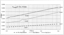
도 1은 3V의 인가전압을 갖는 시험에서 산화아연 두께의 변화에 따른 발생 전류의 변화를 나타낸 그래프이다.
도 2는 3V의 인가전압을 갖는 시험에서 상이한 전극 물질 및 구성에 대해 산화아연 두께의 변화에 따른 발생 전류의 변화를 나타내는 그래프이다.
도 3은 산화아연 층으로부터 방사성 핵종 물질의 거리를 변화시키면서 인가된 전압에 대한 발생 전류의 변화를 나타내는 그래프이다.
도 4는 전원 장치의 제1 실시예의 개략도이다.
도 5는 전원 장치의 다른 실시예의 개략도이다.
도 6은 전원 장치의 또 다른 실시예의 개략도이다.Embodiments of the present invention will now be described with reference to the accompanying drawings.
FIG. 1 is a graph showing a change in generated current according to a change in zinc oxide thickness in a test with an applied voltage of 3 V. FIG.
Figure 2 is a graph showing changes in generated current with changes in zinc oxide thickness for different electrode materials and configurations in tests with an applied voltage of 3V.
3 is a graph showing changes in generated current with respect to an applied voltage while changing the distance of the radionuclide material from the zinc oxide layer.
4 is a schematic diagram of a first embodiment of a power supply.
5 is a schematic diagram of another embodiment of a power supply.
Figure 6 is a schematic diagram of another embodiment of a power supply.
본 발명이 특정한 예시적인 실시예를 참조하여 주로 설명될 것이다. 본 발명의 원리는 도시되고 설명된 특정 구현에 대한 특징의 변형을 사용하여 구현될 수 있음을 이해할 것이다. 실시예는 여기에서 개시된 넓은 발명적 개념을 예시하는 것으로 간주되며 제한하는 것으로 간주되어서는 안 된다.The present invention will be described primarily with reference to specific exemplary embodiments. It is to be understood that the principles of the invention may be implemented using variations of the features for the particular implementation shown and described. The embodiments are to be considered as illustrative of the broad inventive concept disclosed herein and are not to be construed as limitations.
본 발명의 일 구현은 반도체 물질과 접촉하는 금속 전극을 갖는 n형 반도체 물질을 사용하며, 장치를 방사성 핵종 물질로부터의 방사선에 노출시키는 발전 시스템이다. 방사능 방출은 전극과 반도체 물질 사이에 형성된 금속-반도체 접합에서 전기 에너지로 변환된다. 발생된 전기 에너지의 흐름에 있어서, 전극 사이에 전위차가 존재하는 것이 중요하다. 따라서, 하나의 전극에서 다른 전극과 비교하여 더 큰 전하 발생이 생성되도록 하기 위해 전극들 사이의 금속과 반도체 접촉 영역에 상당한 차이가 존재하여야 한다. 더 큰 전하 축적을 갖는 전극은 효과적으로 음의 단자가 되고 다른 전극은 양의 단자가 된다.One embodiment of the present invention is a power generation system that uses an n-type semiconductor material having a metal electrode in contact with a semiconductor material and exposes the device to radiation from a radionuclide material. Radiation emission is converted to electrical energy in the metal-semiconductor junction formed between the electrode and the semiconductor material. In the flow of the generated electric energy, it is important that a potential difference exists between the electrodes. Thus, there must be a significant difference in the metal and semiconductor contact regions between the electrodes in order to produce a larger charge generation at one electrode compared to the other electrode. The electrode having a larger charge accumulation effectively becomes a negative terminal and the other electrode becomes a positive terminal.
방사성 동위원소 전력 셀에서의 전기 발생을 최대화하기 위하여, 비교적 높은 에너지 준위의 방사선원 및 높은 활성 밀도를 사용하는 것이 바람직하다. 그러나, 대부분의 반도체 물질은 이러한 높은 에너지 준위를 견딜 수 없고 노출로 인해 구조적으로 열화된다.In order to maximize the generation of electricity in a radioisotope power cell, it is desirable to use a radiation source of a relatively high energy level and a high active density. However, most semiconductor materials can not withstand such high energy levels and are structurally degraded due to exposure.
산화아연은 n형 반도체이지만, 매우 불량한 반도체 물질로 해당 분야에서는 무시된다. 그러나, 본 발명자는 산화아연이 비교적 높은 에너지 준위의 방사선 및 높은 활성 밀도를 견딜 수 있는 성능을 발휘한다는 것을 발견하였다.Although zinc oxide is an n-type semiconductor, it is a very poor semiconductor material and neglected in the field. However, the present inventors have found that zinc oxide exerts a capability to withstand radiation of a relatively high energy level and a high active density.
제안된 발전 시스템에서 산화아연을 사용하는 초기 시험은 안타깝게도 ZnO가 불량한 반도체 물질이라는 현장에서 인정된 의견에 의해 예상되는 실망스러운 결과를 나타내었다. 높은 준위의 방사능을 견딜 수 있는 능력에도 불구하고, 발생된 전기 출력은 무시할만한 수준이었다.Initial tests using zinc oxide in the proposed power generation system unfortunately showed disappointing results expected by the field-recognized opinion that ZnO is a poor semiconductor material. Despite the ability to withstand high levels of radioactivity, the generated electrical output was negligible.
그러나, 제안된 발전 시스템에서 사용되는 산화아연의 두께를 변화시키면서 시험을 수행하였을 때, 산화아연이 충분히 얇은 층 또는 막의 형태로 제공될 때 놀랍게도 바람직한 결과가 발견되었다. 본 명세서 및 청구범위에서, '얇은'은 약 15㎛ 미만, 바람직하게는 10㎛ 미만을 의미한다.However, surprisingly good results have been found when zinc oxide is provided in the form of a sufficiently thin layer or film when the test is carried out while varying the thickness of zinc oxide used in the proposed power generation system. In the present specification and claims, 'thin' means less than about 15 microns, preferably less than 10 microns.
도 1은 3V의 인가전압을 갖는 시험에서 산화아연 두께의 변화에 따른 발생 전류의 변화를 나타낸 그래프이다. 이 시험에서, 최적의 전류는 1000nm에서였다. FIG. 1 is a graph showing a change in generated current according to a change in zinc oxide thickness in a test with an applied voltage of 3 V. FIG. In this test, the optimum current was at 1000 nm.
실제적인 실험에서, rf 마그네트론 스퍼터링(rf magnetron sputter) 또는 전기 화학 증착에 의해, 5㎝ x 5㎝ 표면을 갖는 기판 상에 산화아연의 박막이 형성되었다. 기판은 유리의 제1층으로 구성된다. 이와 관련하여, 사파이어와 석영 또한 이 제1층에 적합한 것으로 간주된다. 기판은 도핑된 금속 산화물의 층으로 더 구성되며, 이는 산화아연이 증착되는 표면을 형성한다. In a practical experiment, a thin film of zinc oxide was formed on a substrate having a 5 cm x 5 cm surface by rf magnetron sputter or electrochemical deposition. The substrate is comprised of a first layer of glass. In this regard, sapphire and quartz are also considered suitable for this first layer. The substrate is further comprised of a layer of doped metal oxide, which forms the surface on which the zinc oxide is deposited.
이 도핑된 금속 산화물 층은 그 위에 더 작은 양극이 형성될 수 있도록 하여, 양극을 산화아연으로부터 분리시키면서 도핑된 금속 산화물의 반도체 특성으로 인해 전류 경로를 제공한다. 적합한 도핑된 금속 산화물은 불소 도핑된 산화주석 및 주석-도핑 된 산화인듐을 포함하지만, 이에 한정되지 않는다.This doped metal oxide layer allows a smaller anode to be formed thereon to provide an electrical current path due to the semiconductor nature of the doped metal oxide while separating the anode from the zinc oxide. Suitable doped metal oxides include, but are not limited to, fluorine doped tin oxide and tin-doped indium oxide.
다수의 금속 물질, 즉, 금, 구리, 알루미늄 및 은이 전극으로서의 적합성을 위해 시험되었다. 또한, 상이한 전극 구조가 조사되었으며, 첫번째는 전극이 산화아연 층의 전체 표면을 덮는 것이고 두번째로는 산화아연 표면 상에 빗살 모양 또는 손가락 모양의 격자 형성이 사용되었다. 금속 전극 물질의 일반적인 두께는 100-1000nm의 범위이며, 바람직하게는 150nm였다.A number of metallic materials, gold, copper, aluminum and silver, have been tested for their suitability as electrodes. In addition, different electrode structures were investigated, the first one covering the entire surface of the zinc oxide layer and the second one forming a comb or finger-like lattice on the zinc oxide surface. The typical thickness of the metal electrode material is in the range of 100-1000 nm, preferably 150 nm.
금 및 구리는 스퍼터링 기술을 사용하여 증착되었고, 알루미늄 및 은은 열 증착 기술을 사용하여 증착되었다.Gold and copper were deposited using a sputtering technique, and aluminum and silver were deposited using a thermal deposition technique.
상이한 샘플을 Sr-90에 노출시켰다. 금, 알루미늄 및 은이 금속-반도체 접합에서 선형이며 대칭인 전류-전압 곡선을 생성하여 이들 금속과 산화아연 사이의 바람직한 정도의 저항성 접촉을 제시하였다.Different samples were exposed to Sr-90. Gold, aluminum, and silver produced a linear and symmetrical current-voltage curve at the metal-semiconductor junctions, suggesting a desirable degree of resistive contact between these metals and zinc oxide.
구리는 쇼트키 배리어(Schottky barrier)를 나타내는 비선형 및 비대칭 결과를 생성하였으며, 이는 본 목적에 부적합함을 시사한다.Copper produced nonlinear and asymmetrical results indicating Schottky barriers, suggesting that this is unsuitable for this purpose.
상이한 구성에 관해서는, 결과에서 무시할 만한 정도의 차이가 나타났다. 이는 더 적은 금속을 사용하는 빗살 모양의 그리드 구성이 실행 가능한 옵션임을 시사한다. 본 발명의 범위 내에서 다른 기하학 및 구성이 고려될 수 있음을 이해할 것이다.With respect to the different configurations, there was a negligible difference in the results. This suggests that a comb-like grid configuration using fewer metals is a viable option. It is to be understood that other geometries and configurations may be considered within the scope of the present invention.
유사하게, 본 발명은 금속-반도체 접합에서 합금을 포함하여 다른 금속을 사용하여 구현될 수 있음을 이해할 것이다.Similarly, it will be appreciated that the present invention may be implemented using other metals, including alloys, in metal-semiconductor junctions.
150nm와 1500nm 사이의 산화아연 층의 상이한 두께로 시험을 수행하였다.The test was conducted at different thicknesses of the zinc oxide layer between 150 nm and 1500 nm.
두께가 150nm로부터 증가함에 따라 생성되는 전기 출력도 최적 두께가 될 때까지 증가하고, 그 후 두께를 증가시키면 생성되는 전기 출력이 감소되는 놀라운 결과가 나타났다. 약 1500nm를 넘으면, 출력은 실용적인 목적을 위해서는 지나치게 낮아졌다. 결과적으로, 시험은 산화아연의 이상적인 두께 범위가 150nm와 1500nm 사이임을 제시했다. 최적 두께는 물질의 선택에 따라 변하였다.As the thickness increased from 150 nm, the resulting electric power also increased until it reached the optimum thickness, and then the increase in thickness resulted in a surprising result that the electrical output produced was reduced. Beyond about 1500 nm, the output is too low for practical purposes. As a result, the test suggested that the ideal thickness range of zinc oxide is between 150 nm and 1500 nm. The optimum thickness varied depending on the choice of material.
최적 두께는 물질의 선택에 따라 달라졌다. 도 2는 일정한 전압 및 방사선원에서, 상이한 물질 및 물질의 두께로, 두께에 따른 전류의 변화를 도시한다. 물질은 손가락 모양 전극 구성의 은, 전체 전극 구성의 은, 손가락 모양 전극 구성의 알루미늄, 전체 전극 구성의 알루미늄 및 전체 전극 구성의 금을 포함하였다. The optimum thickness varied depending on the choice of material. Figure 2 shows the change in current with thickness, with a constant voltage and source of radiation, with different material and thickness of material. The material included silver in the finger electrode configuration, silver in the overall electrode configuration, aluminum in the finger electrode configuration, aluminum in the overall electrode configuration, and gold in the entire electrode configuration.
특정한 시험에서는 최적 두께가 1000nm이지만, 다른 시험에서는 최적 두께가 1250nm였다(도 1 및 2 참조). 그렇지만, 두께의 전반적인 유용한 범위는 일정하게 유지되었다. 최적 두께는 방사성 핵종 물질의 선택에 따라, 범위 내에서, 또한 변할 수 있을 것으로 예상된다.In the specific test, the optimum thickness was 1000 nm, but in the other tests the optimum thickness was 1250 nm (see FIGS. 1 and 2). However, the overall useful range of thickness has remained constant. The optimum thickness is expected to vary within the range, depending on the choice of radionuclide material.
본 발명의 구현에 사용될 수 있는 다른 베타 방출 물질은 Pm-147, Ni-63 및 삼중 수소, 또는 임의의 다른 적합한 베타 방출 물질을 포함한다. 본 발명은 원칙적으로 다른 종류의 방사성 물질, 예를 들면 X선원, 감마선원 또는 임의의 다른 적합한 물질을 사용할 수 있다. 방사성 핵종은 임의의 적합한 화학적 형태일 수 있으며, 물질은 원칙적으로 상이한 방사성 핵종이나 다른 물질의 혼합물일 수 있다.Other beta emissive materials that may be used in the practice of this invention include Pm-147, Ni-63 and tritium, or any other suitable beta emissive material. The present invention may in principle use other types of radioactive materials, for example X-ray sources, gamma sources or any other suitable material. The radionuclide can be in any suitable chemical form and the material can in principle be a different radionuclide or a mixture of different substances.
도 3에 도시된 바와 같이, 산화아연 층에 대한 Sr-90 물질의 거리 및 입사각을 2mm와 350mm 사이에서 변화시켜 또한 시험을 수행하였다. 도 3은 산화아연 층으로부터 방사성 핵종의 다양한 거리에 대하여, 인가된 전압에 대한 발생 전류의 변화를 나타내는 그래프이다.3, the distance and angle of incidence of the Sr-90 material to the zinc oxide layer were varied between 2 mm and 350 mm and also tested. 3 is a graph showing changes in generated current with respect to an applied voltage for various distances of a radionuclide from a zinc oxide layer.
예상대로, 최상의 출력은 가장 작은 거리에서 발생하였으며 거리가 증가함에 따라 출력이 감소하였다. 그럼에도 불구하고 시험된 범위 전체에 걸쳐, 특히 최대 약 300mm 및 <45°의 각도에서 여전히 상당한 출력이 있었다. 발전기의 두께 치수를 감안할 때, 이는 넓은 공간이며, 동일한 방사성 핵종 물질을 사용하여 여러 개의 발전기 장치가 계층화된 구조로 배열될 수 있으므로, 단일 방사성 핵종원의 전기 출력 용량을 증가시킬 수 있음을 제시한다.As expected, the best output occurred at the smallest distance and the output decreased as the distance increased. Nevertheless, there was still significant power throughout the range tested, especially at angles up to about 300 mm and <45 °. Given the thickness dimensions of the generator, this is a large space, suggesting that multiple generator units can be arranged in a layered structure using the same radionuclide material, thereby increasing the electrical output capacity of a single radial nuclear seed .
발전기 시스템을 사용하는 전원 장치의 실시예가 이제 설명된다.An embodiment of a power supply system using a generator system is now described.
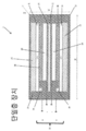
도 4에, 기본 '단일층' 장치(10)가 나타나 있다. 도시된 바와 같이, 장치(10)는 중심에 밀봉된 방사성 핵종(14), 예를 들면 Sr-90, Pm-147, Ni-63 또는 H-3의 층을 갖는 하우징(12)을 포함한다. 하우징(12)은 알루미늄, 강철 등과 같은 다양한 적절한 물질로 형성될 수 있으며, 공기 분위기(28)를 둘러싸고 있다. 밀봉재(16)는 알루미늄, 플라스틱, 마일러(Mylar), 다른 적절한 금속 합금 또는 유사한 저 Z-물질(Z는 원자량임)일 수 있다. 방사성 핵종(14)의 각 측면에는 주석 도핑 된 산화인듐 층(20) 및 그 위에 형성된 산화아연 박층(22)을 갖는 기판(18)(예를 들면, 유리 기판)이 있다. 주석 도핑된 산화인듐의 대안으로 인듐 주석 플루오라이드를 사용할 수 있다. 주 음극(24)은 산화아연(22)의 다른 면에 형성되고 더 작은 양극(26)은 주석 도핑된 산화인듐(20)의 면에 형성된다. 도전성 리드(30)가 양 전극 (24, 26)에 연결되며 부하에 연결하기 위하여 하우징(12)의 외부로 안내한다.In Figure 4, a basic 'single layer'
도 5에는 '이중층' 장치(110)가 나타나 있다. 중앙 방사성 핵종(114)의 각 면은 대응하는 전극(124, 126), 도핑된 금속 산화물 층(120)을 가지며 절연 기판(132)에 의해 분리된 2개의 산화아연 층(122)의 배열을 갖는다.A 'dual layer'
도 6에는 기판 및 ZnO 층이 샌드위치 배열로 배열된 '삼중층' 장치(210)가 나타나 있다. 다른 실시예와 유사하게, 중앙 밀봉된 방사성 핵종(214)은 각 면에 ZnO 층(222), 도핑된 금속 산화물 층(220) 및 전극(224, 226)을 갖는 기판(232)의 3층 배열을 갖는다.FIG. 6 shows a 'triple layer'
이해할 수 있는 바와 같이, 층의 수를 계속 증가시키고, 결과적으로 발생되는 전기 출력을 증가시키는 것이 가능하다. 얼마나 많은 층이 사용될 수 있는지에 대한 한계는 가장 먼 층이 방사성 핵종 물질과 얼마나 멀리 떨어져 있는지에 달려 있다.As can be appreciated, it is possible to continue to increase the number of layers and increase the resulting electrical output. The limit on how many layers can be used depends on how far the farthest layer is from the radionuclide material.
원하는 전력 수준을 제공하기 위하여 하나보다 많은 방사성 핵종 층을 갖는 구조가 추가된 다수의 샌드위치 구조와 함께 사용될 수 있음을 이해할 것이다. 기술된 구조는 일반적으로 정사각형이지만, 적절한 간격이 유지될 수 있다고 가정하면, 구조는 임의의 바람직한 형상일 수 있고, 적절한 구현에서 만곡될 수 있음을 또한 이해할 것이다.It will be appreciated that a structure with more than one radionuclide layer can be used with multiple sandwich structures added to provide the desired power level. Although the structure described is generally square, it will also be appreciated that, assuming that proper spacing can be maintained, the structure can be of any desired shape and can be curved in a suitable implementation.
Claims (17)
n형 반도체 물질의 박층;
적어도 하나는 상기 반도체 물질과 직접 접촉하고 그 사이에 금속-반도체 접합을 형성하는 금속 전극--상기 방사성 핵종 물질로부터 리시브된(received) 방사능 방출이 상기 금속-반도체 접합에서 전기 에너지로 변환됨--; 및
상기 전극에 연결되며 부하에 연결될 때 상기 전기 에너지의 흐름을 용이하게 하는 전기 접점을 포함하는 발전기 시스템.Radionuclide material;
a thin layer of n-type semiconductor material;
At least one of which is a metal electrode that is in direct contact with the semiconductor material and forms a metal-semiconductor junction therebetween, wherein radioactive emissions received from the radionuclide material are converted from the metal-semiconductor junction to electrical energy, ; And
And an electrical contact coupled to the electrode and facilitating the flow of electrical energy when connected to a load.
산화아연 박층;
적어도 하나는 상기 산화아연과 직접 접촉하고 그 사이에 금속-반도체 접합을 형성하는 금속 전극--상기 방사성 핵종 물질로부터 리시브된 방사능 방출이 상기 금속-반도체 접합에서 전기 에너지로 변환됨--; 및
상기 전극에 연결되며 부하에 연결될 때 상기 전기 에너지의 흐름을 용이하게 하는 전기 접점을 포함하는 발전기 시스템.Radionuclide material;
Zinc oxide thin layer;
A metal electrode at least one of which is in direct contact with the zinc oxide and forms a metal-semiconductor junction therebetween, the radioactive emission received from the radionuclide material being converted from the metal-semiconductor junction to electrical energy; And
And an electrical contact coupled to the electrode and facilitating the flow of electrical energy when connected to a load.
Applications Claiming Priority (3)
| Application Number | Priority Date | Filing Date | Title |
|---|---|---|---|
| AU2014904588 | 2014-11-14 | ||
| AU2014904588A AU2014904588A0 (en) | 2014-11-14 | Electrical generator system | |
| PCT/AU2015/050712 WO2016074044A1 (en) | 2014-11-14 | 2015-11-13 | Electrical generator system |
Publications (2)
| Publication Number | Publication Date |
|---|---|
| KR20170120558A true KR20170120558A (en) | 2017-10-31 |
| KR102544103B1 KR102544103B1 (en) | 2023-06-16 |
Family
ID=55953471
Family Applications (1)
| Application Number | Title | Priority Date | Filing Date |
|---|---|---|---|
| KR1020177016357A KR102544103B1 (en) | 2014-11-14 | 2015-11-13 | Electrical generator system |
Country Status (19)
| Country | Link |
|---|---|
| US (1) | US10784010B2 (en) |
| EP (1) | EP3218906B1 (en) |
| JP (1) | JP6647312B2 (en) |
| KR (1) | KR102544103B1 (en) |
| CN (1) | CN107210078B (en) |
| AU (1) | AU2015346007B2 (en) |
| BR (1) | BR112017010158B1 (en) |
| CA (1) | CA3005098A1 (en) |
| DK (1) | DK3218906T3 (en) |
| ES (1) | ES2752731T3 (en) |
| HR (1) | HRP20191930T1 (en) |
| HU (1) | HUE047151T2 (en) |
| MY (1) | MY189288A (en) |
| NZ (1) | NZ732851A (en) |
| PL (1) | PL3218906T3 (en) |
| PT (1) | PT3218906T (en) |
| RU (1) | RU2704321C2 (en) |
| SG (1) | SG11201703731XA (en) |
| WO (1) | WO2016074044A1 (en) |
Families Citing this family (5)
| Publication number | Priority date | Publication date | Assignee | Title |
|---|---|---|---|---|
| RU2632588C1 (en) * | 2016-08-04 | 2017-10-06 | Федеральное государственное унитарное предприятие "Горно-химический комбинат" (ФГУП "ГХК") | Beta-voltaic battery |
| RU2731368C1 (en) * | 2019-09-30 | 2020-09-02 | Алан Кулкаев | Radioisotopic photoelectric generator |
| US20220139588A1 (en) * | 2020-11-04 | 2022-05-05 | Westinghouse Electric Company Llc | Nuclear battery |
| US20220199272A1 (en) * | 2020-12-17 | 2022-06-23 | Westinghouse Electric Company Llc | Methods of manufacture for nuclear batteries |
| WO2023108220A1 (en) * | 2021-12-16 | 2023-06-22 | Infinite Power Company Limited | Electrical generator system |
Citations (4)
| Publication number | Priority date | Publication date | Assignee | Title |
|---|---|---|---|---|
| JPH02114193A (en) * | 1988-10-24 | 1990-04-26 | Showa Denko Kk | Manufacture of thin film radiation detector |
| JP2003279691A (en) * | 2002-03-26 | 2003-10-02 | Toshiba Corp | Radiation-current transducing device and method thereof |
| JP2012520466A (en) * | 2009-03-12 | 2012-09-06 | ザ キュレイターズ オブ ザ ユニヴァーシティー オブ ミズーリ | High energy density radioisotope micro power supply |
| US20120326164A1 (en) * | 2009-11-19 | 2012-12-27 | Cornell University | Betavoltaic apparatus and method |
Family Cites Families (17)
| Publication number | Priority date | Publication date | Assignee | Title |
|---|---|---|---|---|
| US2847585A (en) * | 1952-10-31 | 1958-08-12 | Rca Corp | Radiation responsive voltage sources |
| JPS5247349B2 (en) * | 1971-09-17 | 1977-12-01 | ||
| US5721462A (en) | 1993-11-08 | 1998-02-24 | Iowa State University Research Foundation, Inc. | Nuclear battery |
| US5642014A (en) * | 1995-09-27 | 1997-06-24 | Lucent Technologies Inc. | Self-powered device |
| US6118204A (en) * | 1999-02-01 | 2000-09-12 | Brown; Paul M. | Layered metal foil semiconductor power device |
| JP2002196099A (en) * | 2000-12-25 | 2002-07-10 | Yutaka Arima | alpha-RAY RADIATION TYPE SOLAR CELL |
| US6479919B1 (en) * | 2001-04-09 | 2002-11-12 | Terrence L. Aselage | Beta cell device using icosahedral boride compounds |
| US6774531B1 (en) * | 2003-01-31 | 2004-08-10 | Betabatt, Inc. | Apparatus and method for generating electrical current from the nuclear decay process of a radioactive material |
| US7002179B2 (en) * | 2003-03-14 | 2006-02-21 | Rohm Co., Ltd. | ZnO system semiconductor device |
| CN101527175B (en) * | 2009-04-10 | 2011-10-12 | 中国科学院苏州纳米技术与纳米仿生研究所 | PIN type nuclear battery and preparation method thereof |
| US8487392B2 (en) * | 2009-08-06 | 2013-07-16 | Widetronix, Inc. | High power density betavoltaic battery |
| US9183960B2 (en) * | 2010-05-28 | 2015-11-10 | Medtronic, Inc. | Betavoltaic power converter die stacking |
| US20130098440A1 (en) * | 2010-06-29 | 2013-04-25 | Yeda Research And Development Co. Ltd. | Photovoltaic cell and method of its manufacture |
| RU2461915C1 (en) * | 2011-04-28 | 2012-09-20 | Государственное образовательное учреждение высшего профессионального образования Томский государственный университет (ТГУ) | Nuclear battery |
| CN105050679B (en) * | 2013-01-31 | 2017-09-29 | 密苏里大学管委会 | Radiolysis electrochemical generator |
| CN103730181A (en) * | 2013-10-26 | 2014-04-16 | 溧阳市浙大产学研服务中心有限公司 | Method for manufacturing silicon carbide Schottky junction nuclear battery |
| WO2015153187A1 (en) * | 2014-03-31 | 2015-10-08 | Medtronic, Inc. | Nuclear radiation particle power converter |
-
2015
- 2015-11-13 NZ NZ732851A patent/NZ732851A/en active IP Right Revival
- 2015-11-13 MY MYPI2017701630A patent/MY189288A/en unknown
- 2015-11-13 CN CN201580073585.2A patent/CN107210078B/en active Active
- 2015-11-13 JP JP2017544804A patent/JP6647312B2/en active Active
- 2015-11-13 KR KR1020177016357A patent/KR102544103B1/en active IP Right Grant
- 2015-11-13 PL PL15859904T patent/PL3218906T3/en unknown
- 2015-11-13 CA CA3005098A patent/CA3005098A1/en active Pending
- 2015-11-13 RU RU2017120840A patent/RU2704321C2/en active
- 2015-11-13 US US15/526,012 patent/US10784010B2/en active Active
- 2015-11-13 EP EP15859904.3A patent/EP3218906B1/en active Active
- 2015-11-13 HU HUE15859904A patent/HUE047151T2/en unknown
- 2015-11-13 DK DK15859904.3T patent/DK3218906T3/en active
- 2015-11-13 BR BR112017010158-0A patent/BR112017010158B1/en active IP Right Grant
- 2015-11-13 ES ES15859904T patent/ES2752731T3/en active Active
- 2015-11-13 AU AU2015346007A patent/AU2015346007B2/en active Active
- 2015-11-13 SG SG11201703731XA patent/SG11201703731XA/en unknown
- 2015-11-13 WO PCT/AU2015/050712 patent/WO2016074044A1/en active Application Filing
- 2015-11-13 PT PT158599043T patent/PT3218906T/en unknown
-
2019
- 2019-10-23 HR HRP20191930TT patent/HRP20191930T1/en unknown
Patent Citations (4)
| Publication number | Priority date | Publication date | Assignee | Title |
|---|---|---|---|---|
| JPH02114193A (en) * | 1988-10-24 | 1990-04-26 | Showa Denko Kk | Manufacture of thin film radiation detector |
| JP2003279691A (en) * | 2002-03-26 | 2003-10-02 | Toshiba Corp | Radiation-current transducing device and method thereof |
| JP2012520466A (en) * | 2009-03-12 | 2012-09-06 | ザ キュレイターズ オブ ザ ユニヴァーシティー オブ ミズーリ | High energy density radioisotope micro power supply |
| US20120326164A1 (en) * | 2009-11-19 | 2012-12-27 | Cornell University | Betavoltaic apparatus and method |
Also Published As
| Publication number | Publication date |
|---|---|
| AU2015346007B2 (en) | 2020-04-16 |
| BR112017010158B1 (en) | 2022-11-08 |
| EP3218906A1 (en) | 2017-09-20 |
| BR112017010158A2 (en) | 2018-02-14 |
| HUE047151T2 (en) | 2020-04-28 |
| ES2752731T3 (en) | 2020-04-06 |
| PT3218906T (en) | 2019-10-31 |
| KR102544103B1 (en) | 2023-06-16 |
| CN107210078A (en) | 2017-09-26 |
| CA3005098A1 (en) | 2016-05-19 |
| MY189288A (en) | 2022-01-31 |
| RU2017120840A (en) | 2018-12-18 |
| EP3218906B1 (en) | 2019-07-10 |
| CN107210078B (en) | 2019-07-05 |
| US10784010B2 (en) | 2020-09-22 |
| NZ732851A (en) | 2021-12-24 |
| HRP20191930T1 (en) | 2020-04-03 |
| RU2017120840A3 (en) | 2019-06-04 |
| RU2704321C2 (en) | 2019-10-28 |
| SG11201703731XA (en) | 2017-06-29 |
| AU2015346007A1 (en) | 2017-07-06 |
| JP6647312B2 (en) | 2020-02-14 |
| US20170309359A1 (en) | 2017-10-26 |
| WO2016074044A1 (en) | 2016-05-19 |
| JP2017535796A (en) | 2017-11-30 |
| DK3218906T3 (en) | 2019-10-21 |
| PL3218906T3 (en) | 2020-03-31 |
| EP3218906A4 (en) | 2018-07-11 |
Similar Documents
| Publication | Publication Date | Title |
|---|---|---|
| KR102544103B1 (en) | Electrical generator system | |
| US4024420A (en) | Deep diode atomic battery | |
| US8866152B2 (en) | Betavoltaic apparatus and method | |
| US6479919B1 (en) | Beta cell device using icosahedral boride compounds | |
| US6238812B1 (en) | Isotopic semiconductor batteries | |
| US5087533A (en) | Contact potential difference cell | |
| US6118204A (en) | Layered metal foil semiconductor power device | |
| EP2406793B1 (en) | High energy-density radioisotope micro power sources | |
| US20130154438A1 (en) | Power-Scalable Betavoltaic Battery | |
| US4010534A (en) | Process for making a deep diode atomic battery | |
| RU2539109C1 (en) | Multijunction silicone monocrystalline converter of optic and radiation emissions | |
| US10699820B2 (en) | Three dimensional radioisotope battery and methods of making the same | |
| US20180024254A1 (en) | Radiation detector | |
| KR102134223B1 (en) | Beta battery | |
| US3824448A (en) | Contact potential generator system | |
| OA18273A (en) | Electrical generator system. | |
| US3538356A (en) | Energy converter | |
| RU2605758C1 (en) | Electric power supply source | |
| GB2484028A (en) | Power-Scalable Betavoltaic Battery | |
| WO2023108220A1 (en) | Electrical generator system | |
| RU2641100C1 (en) | COMPACT BETAVOLTAIC POWER SUPPLY OF LONG USE WITH BETA EMITTER ON BASIS OF RADIOISOTOPE 63 Ni AND METHOD OF OBTAINING IT | |
| RU2670710C1 (en) | Radioisotope element of electric power supply with semiconductor converter, combined with radiation source | |
| EP0035578B1 (en) | Electromagnetic radiation transducer module | |
| KR20140098897A (en) | The atomic cell using radiation shielding material | |
| Tse | Si--Au Schottky barrier nuclear battery |
Legal Events
| Date | Code | Title | Description |
|---|---|---|---|
| E902 | Notification of reason for refusal | ||
| E701 | Decision to grant or registration of patent right | ||
| GRNT | Written decision to grant |