KR20170114440A - Current circuit breaker - Google Patents
Current circuit breaker Download PDFInfo
- Publication number
- KR20170114440A KR20170114440A KR1020160041254A KR20160041254A KR20170114440A KR 20170114440 A KR20170114440 A KR 20170114440A KR 1020160041254 A KR1020160041254 A KR 1020160041254A KR 20160041254 A KR20160041254 A KR 20160041254A KR 20170114440 A KR20170114440 A KR 20170114440A
- Authority
- KR
- South Korea
- Prior art keywords
- switch
- current
- semiconductor module
- capacitor
- opened
- Prior art date
Links
Images


Classifications
-
- H—ELECTRICITY
- H02—GENERATION; CONVERSION OR DISTRIBUTION OF ELECTRIC POWER
- H02H—EMERGENCY PROTECTIVE CIRCUIT ARRANGEMENTS
- H02H3/00—Emergency protective circuit arrangements for automatic disconnection directly responsive to an undesired change from normal electric working condition with or without subsequent reconnection ; integrated protection
- H02H3/08—Emergency protective circuit arrangements for automatic disconnection directly responsive to an undesired change from normal electric working condition with or without subsequent reconnection ; integrated protection responsive to excess current
- H02H3/093—Emergency protective circuit arrangements for automatic disconnection directly responsive to an undesired change from normal electric working condition with or without subsequent reconnection ; integrated protection responsive to excess current with timing means
-
- H—ELECTRICITY
- H02—GENERATION; CONVERSION OR DISTRIBUTION OF ELECTRIC POWER
- H02H—EMERGENCY PROTECTIVE CIRCUIT ARRANGEMENTS
- H02H9/00—Emergency protective circuit arrangements for limiting excess current or voltage without disconnection
- H02H9/02—Emergency protective circuit arrangements for limiting excess current or voltage without disconnection responsive to excess current
-
- H—ELECTRICITY
- H02—GENERATION; CONVERSION OR DISTRIBUTION OF ELECTRIC POWER
- H02H—EMERGENCY PROTECTIVE CIRCUIT ARRANGEMENTS
- H02H3/00—Emergency protective circuit arrangements for automatic disconnection directly responsive to an undesired change from normal electric working condition with or without subsequent reconnection ; integrated protection
- H02H3/08—Emergency protective circuit arrangements for automatic disconnection directly responsive to an undesired change from normal electric working condition with or without subsequent reconnection ; integrated protection responsive to excess current
- H02H3/10—Emergency protective circuit arrangements for automatic disconnection directly responsive to an undesired change from normal electric working condition with or without subsequent reconnection ; integrated protection responsive to excess current additionally responsive to some other abnormal electrical conditions
- H02H3/105—Emergency protective circuit arrangements for automatic disconnection directly responsive to an undesired change from normal electric working condition with or without subsequent reconnection ; integrated protection responsive to excess current additionally responsive to some other abnormal electrical conditions responsive to excess current and fault current to earth
-
- G—PHYSICS
- G01—MEASURING; TESTING
- G01R—MEASURING ELECTRIC VARIABLES; MEASURING MAGNETIC VARIABLES
- G01R31/00—Arrangements for testing electric properties; Arrangements for locating electric faults; Arrangements for electrical testing characterised by what is being tested not provided for elsewhere
- G01R31/327—Testing of circuit interrupters, switches or circuit-breakers
- G01R31/3271—Testing of circuit interrupters, switches or circuit-breakers of high voltage or medium voltage devices
- G01R31/3275—Fault detection or status indication
-
- H—ELECTRICITY
- H01—ELECTRIC ELEMENTS
- H01H—ELECTRIC SWITCHES; RELAYS; SELECTORS; EMERGENCY PROTECTIVE DEVICES
- H01H33/00—High-tension or heavy-current switches with arc-extinguishing or arc-preventing means
- H01H33/02—Details
- H01H33/59—Circuit arrangements not adapted to a particular application of the switch and not otherwise provided for, e.g. for ensuring operation of the switch at a predetermined point in the ac cycle
- H01H33/596—Circuit arrangements not adapted to a particular application of the switch and not otherwise provided for, e.g. for ensuring operation of the switch at a predetermined point in the ac cycle for interrupting dc
-
- H—ELECTRICITY
- H01—ELECTRIC ELEMENTS
- H01H—ELECTRIC SWITCHES; RELAYS; SELECTORS; EMERGENCY PROTECTIVE DEVICES
- H01H9/00—Details of switching devices, not covered by groups H01H1/00 - H01H7/00
- H01H9/54—Circuit arrangements not adapted to a particular application of the switching device and for which no provision exists elsewhere
- H01H9/548—Electromechanical and static switch connected in series
-
- H—ELECTRICITY
- H02—GENERATION; CONVERSION OR DISTRIBUTION OF ELECTRIC POWER
- H02H—EMERGENCY PROTECTIVE CIRCUIT ARRANGEMENTS
- H02H3/00—Emergency protective circuit arrangements for automatic disconnection directly responsive to an undesired change from normal electric working condition with or without subsequent reconnection ; integrated protection
- H02H3/08—Emergency protective circuit arrangements for automatic disconnection directly responsive to an undesired change from normal electric working condition with or without subsequent reconnection ; integrated protection responsive to excess current
- H02H3/087—Emergency protective circuit arrangements for automatic disconnection directly responsive to an undesired change from normal electric working condition with or without subsequent reconnection ; integrated protection responsive to excess current for dc applications
-
- H—ELECTRICITY
- H02—GENERATION; CONVERSION OR DISTRIBUTION OF ELECTRIC POWER
- H02H—EMERGENCY PROTECTIVE CIRCUIT ARRANGEMENTS
- H02H7/00—Emergency protective circuit arrangements specially adapted for specific types of electric machines or apparatus or for sectionalised protection of cable or line systems, and effecting automatic switching in the event of an undesired change from normal working conditions
- H02H7/008—Emergency protective circuit arrangements specially adapted for specific types of electric machines or apparatus or for sectionalised protection of cable or line systems, and effecting automatic switching in the event of an undesired change from normal working conditions for protective arrangements according to this subclass
-
- H—ELECTRICITY
- H02—GENERATION; CONVERSION OR DISTRIBUTION OF ELECTRIC POWER
- H02H—EMERGENCY PROTECTIVE CIRCUIT ARRANGEMENTS
- H02H9/00—Emergency protective circuit arrangements for limiting excess current or voltage without disconnection
- H02H9/04—Emergency protective circuit arrangements for limiting excess current or voltage without disconnection responsive to excess voltage
- H02H9/044—Physical layout, materials not provided for elsewhere
-
- H—ELECTRICITY
- H01—ELECTRIC ELEMENTS
- H01H—ELECTRIC SWITCHES; RELAYS; SELECTORS; EMERGENCY PROTECTIVE DEVICES
- H01H9/00—Details of switching devices, not covered by groups H01H1/00 - H01H7/00
- H01H9/54—Circuit arrangements not adapted to a particular application of the switching device and for which no provision exists elsewhere
- H01H9/541—Contacts shunted by semiconductor devices
- H01H9/542—Contacts shunted by static switch means
- H01H2009/543—Contacts shunted by static switch means third parallel branch comprising an energy absorber, e.g. MOV, PTC, Zener
Abstract
본 발명은 전류 차단기에 관한 것으로, 보다 상세하게는 고속 스위치를 이용하여 전류를 차단함으로써 반도체 모듈을 보호하기 위한 전류 차단기에 관한 것이다. 본 발명의 일 실시예에 따른 전류 차단기는 고장 전류가 발생하면 개방되는 제1 스위치, 상기 제1 스위치와 연결되고 상기 제1 스위치가 개방되는 시점부터 미리 설정된 시간 이후에 개방되는 제2 스위치, 일단은 상기 제1 스위치와 연결되고, 타단은 상기 제2 스위치와 연결되는 반도체 모듈, 일단은 상기 제2 스위치와 연결되고 타단은 상기 반도체 모듈과 연결되는 캐패시터 및 상기 캐패시터의 양단과 연결되고 상기 캐패시터의 양단 전압에 따라 저항 값을 변경하여 상기 고장 전류를 차단하는 어레스터를 포함한다.BACKGROUND OF THE INVENTION 1. Field of the Invention The present invention relates to a current circuit breaker, and more particularly, to a current circuit breaker for protecting a semiconductor module by blocking a current using a high-speed switch. A current breaker according to an embodiment of the present invention includes a first switch that is opened when a fault current is generated, a second switch that is connected to the first switch and opens after a predetermined time from when the first switch is opened, A semiconductor module having one end connected to the second switch and the other end connected to the semiconductor module; and a capacitor connected to both ends of the capacitor, the capacitor being connected to the first switch, And an arrestor for interrupting the fault current by changing the resistance value according to the both-end voltage.
Description
본 발명은 전류 차단기에 관한 것으로, 보다 상세하게는 고속 스위치를 이용하여 전류를 차단함으로써 반도체 모듈을 보호하기 위한 전류 차단기에 관한 것이다.BACKGROUND OF THE INVENTION 1. Field of the Invention The present invention relates to a current circuit breaker, and more particularly, to a current circuit breaker for protecting a semiconductor module by blocking a current using a high-speed switch.
전류 차단기란 송변전 계통이나 전기회로에서 부하를 개폐하거나 접지, 단락 등의 사고가 발생할 경우 전류를 차단시키는 기기이다. 전류 차단기는 차단부가 절연물로 절연되어 조립된 경우 통상 사용 상태의 선로를 수동으로 개폐할 수 있다. 또한, 전류 차단기는 금속용기 외부의 전기조작장치 등에 의하여 원거리에서 개폐할 수 있고, 과부하 및 단락 시 자동적으로 선로를 차단하여 전력계통과 부하기기를 보호할 수 있다.The current breaker is a device that cuts off the current in case of an accident such as opening or closing of the load or grounding or short circuit in the transmission line or electric circuit. The circuit breaker can be manually opened and closed in a normally used line when the circuit breaker is assembled with insulation insulated. In addition, the current breaker can be opened and closed at a remote location by an electric control device outside the metal container, etc., and can automatically protect the power system and the load device by shutting off the line at the time of overload and short circuit.
도 1은 종래의 전류 차단기(10)를 도시한 도면이다. 도 1을 참조하여 종래의 전류 차단기(10) 동작 과정을 설명하면, 정상 전류가 흐를 때에는 스위치(12)가 단락되고 정상 전류는 주회로의 전력용 반도체(11)를 통해 흐른다. 또한, 정상 전류가 흐를 때에는 반도체 모듈(13)은 턴 오프 상태이므로 반도체 모듈(13)을 통해서는 정상 전류가 흐르지 않는다. 이 때 반도체 모듈(13)은 다수의 전력용 반도체(11)가 결합한 집합체일 수 있다.1 is a view showing a conventional
그러나 고압직류 송전 또는 배전 선로에서 기기의 보수, 교체 및 고장 전류가 발생하면 전류를 차단하기 위해 반도체 모듈(13)이 턴 온 된다. 반도체 모듈(13)이 턴 온 되면, 주회로의 전력용 반도체(11)는 턴 오프 되고 스위치(12)가 개방된다. 스위치(12)가 개방 되면 고장 전류는 반도체 모듈(13)을 통해 흐르게 되는데, 이 때 반도체 모듈(13)을 턴 오프 시켜 고장 전류를 차단한다. However, when maintenance, replacement and fault current occur in the high voltage direct current transmission or distribution line, the
다시 도 1을 참조하면, 종래의 전류 차단기(10)는 전류를 차단하기 위해 다수의 전력용 반도체(11)가 필요하다. 따라서, 종래의 전류 차단기(10)에 따르면 전류를 차단하기 위해 많은 비용이 발생한다는 문제점이 있다. 또한, 종래의 전류 차단기(10)에 따르면 다수의 전력용 반도체(11)로 인해 전류 차단기(10)의 부피가 커진다는 문제점이 있다. 또한, 종래의 전류 차단기(10)에 따르면 전력용 반도체(11)에서 발열이 발생하여 냉각장치가 필요하다는 문제점이 있다.Referring again to FIG. 1, a conventional
본 발명은 고속 스위치를 이용하여 전류를 차단함으로써 반도체 모듈을 보호하기 위한 전류 차단기를 제공하는 것을 목적으로 한다.An object of the present invention is to provide a current interrupter for protecting a semiconductor module by interrupting a current using a high-speed switch.
또한, 본 발명은 우회 회로를 이용하여 전류를 차단함으로써 전력용 반도체의 수를 줄일 수 있는 전류 차단기를 제공하는 것을 목적으로 한다.Another object of the present invention is to provide a current interrupter capable of reducing the number of power semiconductors by cutting off current by using a bypass circuit.
또한, 본 발명은 우회 회로를 이용하여 전류를 차단함으로써 전류 차단기의 부피를 줄이고 제작 비용을 감소시킬 수 있는 전류 차단기를 제공하는 것을 목적으로 한다.Another object of the present invention is to provide a current circuit breaker which can reduce the volume of the current circuit breaker and reduce the manufacturing cost by blocking the current using a bypass circuit.
또한, 본 발명은 우회 회로를 이용하여 전류를 차단함으로써 발열을 감소시킬 수 있는 전류 차단기를 제공하는 것을 목적으로 한다. Another object of the present invention is to provide a current circuit breaker capable of reducing heat generation by interrupting a current using a bypass circuit.
이러한 목적을 달성하기 위한 본 발명의 일 실시예에 따른 전류 차단기는 고장 전류가 발생하면 개방되는 제1 스위치, 상기 제1 스위치와 연결되고 상기 제1 스위치가 개방되는 시점부터 미리 설정된 시간 이후에 개방되는 제2 스위치, 일단은 상기 제1 스위치와 연결되고, 타단은 상기 제2 스위치와 연결되는 반도체 모듈, 일단은 상기 제2 스위치와 연결되고 타단은 상기 반도체 모듈과 연결되는 캐패시터 및 상기 캐패시터의 양단과 연결되고 상기 캐패시터의 양단 전압에 따라 저항 값을 변경하여 상기 고장 전류를 차단하는 어레스터를 포함하는 것을 특징으로 한다.According to an aspect of the present invention, there is provided a current circuit breaker including a first switch that is opened when a fault current is generated, a first switch connected to the first switch, A semiconductor module having one end connected to the first switch and the other end connected to the second switch, a capacitor having one end connected to the second switch and the other end connected to the semiconductor module, And an arrestor connected to the capacitor and for interrupting the fault current by changing a resistance value according to a voltage across the capacitor.
전술한 바와 같은 본 발명에 의하면 고속 스위치를 이용하여 전류를 차단함으로써 반도체 모듈을 보호할 수 있는 효과가 있다.According to the present invention as described above, the semiconductor module can be protected by blocking the current using the high-speed switch.
또한, 본 발명에 의하면 우회 회로를 이용하여 전류를 차단함으로써 전력용 반도체의 수를 줄일 수 있는 효과가 있다.Further, according to the present invention, there is an effect that the number of power semiconductors can be reduced by cutting off current by using a bypass circuit.
또한, 본 발명은 우회 회로를 이용하여 전류를 차단함으로써 전류 차단기의 부피를 줄이고 제작 비용을 감소시킬 수 있는 효과가 있다.Further, the present invention has the effect of reducing the volume of the current breaker and reducing the manufacturing cost by cutting off current by using a bypass circuit.
또한, 본 발명은 우회 회로를 이용하여 전류를 차단함으로써 발열을 감소시킬 수 있는 효과가 있다. Further, the present invention has an effect of reducing the heat generation by cutting off current by using a bypass circuit.
도 1은 종래의 전류 차단기를 도시한 도면.
도 2는 본 발명의 일 실시예에 따른 전류 차단기를 도시한 도면.
도 3은 본 발명의 일 실시예에 따른 제1 스위치 및 스트로크를 도시한 도면.
도 4는 제1 스위치가 완전 개방 되면 제어부가 제2 스위치를 개방하는 모습을 도시한 도면.
도 5는 본 발명의 일 실시예에 따른 주회로에 정상 전류가 흐르는 모습을 도시한 도면.
도 6은 본 발명의 일 실시예에 따른 주회로에 고장 전류가 흐르는 모습을 도시한 도면.
도 7은 본 발명의 일 실시예에 따른 제2 스위치 및 반도체 모듈에 고장 전류가 흐르는 모습을 도시한 도면.
도 8은 본 발명의 일 실시예에 따른 캐패시터에 고장 전류가 흐르는 모습을 도시한 도면.
도 9는 본 발명의 일 실시예에 따른 어레스터에 고장 전류가 흐르는 모습을 도시한 도면.
도 10은 본 발명의 일 실시예에 따른 고장 전류의 크기를 도시한 그래프.1 shows a conventional current breaker.
2 illustrates a current breaker in accordance with an embodiment of the present invention.
3 illustrates a first switch and a stroke according to one embodiment of the present invention.
4 is a view showing a state in which the control unit opens the second switch when the first switch is fully opened.
5 is a view showing a state where a normal current flows in a main circuit according to an embodiment of the present invention;
6 is a view showing a state where a fault current flows in a main circuit according to an embodiment of the present invention;
7 is a view showing a state where a fault current flows in a second switch and a semiconductor module according to an embodiment of the present invention.
FIG. 8 is a view showing a state where a fault current flows in a capacitor according to an embodiment of the present invention; FIG.
9 is a view showing a state where a fault current flows in an arrestor according to an embodiment of the present invention.
10 is a graph showing the magnitude of a fault current according to an embodiment of the present invention.
전술한 목적, 특징 및 장점은 첨부된 도면을 참조하여 상세하게 후술되며, 이에 따라 본 발명이 속하는 기술분야에서 통상의 지식을 가진 자가 본 발명의 기술적 사상을 용이하게 실시할 수 있을 것이다. 본 발명을 설명함에 있어서 본 발명과 관련된 공지 기술에 대한 구체적인 설명이 본 발명의 요지를 불필요하게 흐릴 수 있다고 판단되는 경우에는 상세한 설명을 생략한다. 이하, 첨부된 도면을 참조하여 본 발명에 따른 바람직한 실시예를 상세히 설명하기로 한다. 도면에서 동일한 참조부호는 동일 또는 유사한 구성요소를 가리키는 것으로 사용된다.The above and other objects, features, and advantages of the present invention will become more apparent by describing in detail exemplary embodiments thereof with reference to the attached drawings, which are not intended to limit the scope of the present invention. In the following description, well-known functions or constructions are not described in detail since they would obscure the invention in unnecessary detail. Hereinafter, preferred embodiments of the present invention will be described in detail with reference to the accompanying drawings. In the drawings, the same reference numerals are used to denote the same or similar elements.
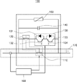
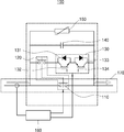
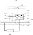
도 2는 본 발명의 일 실시예에 따른 전류 차단기(100)를 도시한 도면이다. 도 2를 참조하면, 본 발명의 일 실시예에 따른 전류 차단기(100)는 제1 스위치(110), 제2 스위치(120), 반도체 모듈(130), 캐패시터(140), 어레스터(150) 및 제어부(160)를 포함하여 구성될 수 있다. 도 2에 도시된 전류 차단기(100)는 일 실시예에 따른 것이고, 그 구성요소들이 도 2에 도시된 실시 예에 한정되는 것은 아니며, 필요에 따라 일부 구성요소가 부가, 변경 또는 삭제될 수 있다. 도 3은 본 발명의 일 실시예에 따른 제1 스위치(110) 및 스트로크(111)를 도시한 도면이고, 도 4는 제1 스위치가 완전 개방 되면 제어부가 제2 스위치를 개방하는 모습을 도시한 도면이다. 이하 도 2 내지 도 4를 참조하여 본 발명의 일 실시예에 따른 전류 차단기(100)를 설명하도록 한다.2 is a view illustrating a
제1 스위치(110)는 고장 전류가 발생하면 개방될 수 있다. 이때 제1 스위치(110)는 고속 스위치일 수 있고 고장 전류 또는 정상 전류가 흐르는지 여부에 따라 주회로(170)의 양단을 개방 또는 단락 시킬 수 있다. 즉, 제1 스위치(110)는 주회로(170)에 고장 전류가 흐르면 개방되고, 주회로(170)에 정상 전류가 흐르면 단락된다. 이 때 고장 전류는 고압직류 송전 또는 배전 선로에서 기기의 보수, 교체 시 발생하는 전류로서 정상 전류보다 큰 값을 가질 수 있다. The
제2 스위치(120)는 제1 스위치(110)와 연결될 수 있고, 제2 스위치(120)는 고속 스위치일 수 있다. 제2 스위치(120)와 제1 스위치(110)의 종류는 동일할 수 있고, 제2 스위치(120)는 제1 스위치(110)가 개방되는 시점부터 미리 설정된 시간 이후에 개방될 수 있다. 미리 설정된 시간은 사용자에 의해 설정될 수 있고, 제어부에서 자동으로 설정할 수도 있다.The
일 실시예로, 제2 스위치(120)는 반도체 모듈(130)이 턴 온 되면 개방되어 고장 전류를 차단할 수 있다. 즉, 고장 전류가 주회로(170)를 통해 흐르게 되면 제1 스위치(110)가 개방되고, 반도체 모듈(130)이 턴 온 된다. 반도체 모듈(130)이 턴 온 되면 고장 전류가 반도체 모듈(130)을 통해 흐르게 되고, 이 때 제 2 스위치(120)가 개방되어 우회 회로를 통해 흐르는 고장 전류를 차단시킬 수 있다. 한편, 제2 스위치(120)가 개방된 후에는 반도체 모듈(130)이 턴 오프 되는데 이에 대해서는 후술하도록 한다. In one embodiment, the
한편, 미리 설정된 시간은 제1 스위치(110)의 스트로크(111)에 비례할 수 있다. 스트로크(111)란 제1 스위치(110)의 한 끝에서 다른 끝까지 움직이는 거리로서 도 3에서 거리(111)일 수 있다. 예를 들어, 제1 스위치(110)의 스트로크(111)가 길수록 제2 스위치(120)는 제1 스위치(110)가 개방된 시점부터 더 긴 시간 이후 개방될 수 있다. 또한, 제1 스위치(110)의 스트로크(111)가 짧을수록 제2 스위치(120)는 제1 스위치(110)가 개방된 시점부터 더 짧은 시간 내에 개방될 수 있다.On the other hand, the preset time may be proportional to the
반도체 모듈(130)은 일단은 제1 스위치(110)와 연결되고, 타단은 제2 스위치(120)와 연결될 수 있다. 반도체 모듈(130)은 제1 스위치(110)는 개방되고, 제2 스위치(120)는 단락된 상태에서 턴 온 되어 고장 전류를 흐르게 할 수 있는 모듈로서 하나 이상의 다이오드 및 하나 이상의 트랜지스터를 포함할 수 있다. 또한, 반도체 모듈(130)은 제2 스위치(120)가 개방된 후 턴 오프 되어 고장 전류를 캐패시터(140)로 흐르게 할 수 있다. 이때 트랜지스터는 MOSFET, BJT, IGBT 등일 수 있고 트랜지스터의 종류는 한정하지 않는다.The
일 실시예로 반도체 모듈(130)은 제1 다이오드(131), 제1 다이오드(131)와 반대 방향으로 배치되는 제2 다이오드(133)를 포함할 수 있다. 또한, 반도체 모듈(130)은 제1 다이오드(131)의 반대 방향으로 제1 다이오드(131)의 양단과 연결되는 제1 트랜지스터(132) 및 제2 다이오드(133)의 반대 방향으로 제2 다이오드(133)의 양단과 연결되는 제2 트랜지스터(134)를 포함할 수 있다. 도 2에 도시된 반도체 모듈(130)과 같이 회로를 구성하는 이유는 양 방향에서 흐르는 고장 전류를 제어하기 위함이다.The
예를 들어, 고장 전류가 왼쪽에서 오른쪽으로 흐를 경우, 고장 전류는 제2 스위치(120), 제1 트랜지스터(132) 및 제2 다이오드(133)를 통해 흐른다. 반대로 고장 전류가 오른쪽에서 왼쪽으로 흐를 경우, 고장 전류는 제2 트랜지스터(134), 제1 다이오드(131) 및 제2 스위치(120)를 통해 흐르게 된다. For example, when a fault current flows from left to right, a fault current flows through the
한편, 우회 회로는 제2 스위치(120) 및 반도체 모듈(130)은 포함하는 회로로서, 본 발명에 의하면 우회 회로를 이용하여 전류를 차단함으로써 전력용 반도체의 수를 줄일 수 있는 효과가 있다. 또한, 본 발명은 우회 회로를 이용하여 전류를 차단함으로써 전류 차단기(100)의 부피를 줄이고 제작 비용을 감소시킬 수 있는 효과가 있다.On the other hand, the bypass circuit includes the
캐패시터(140)는 일단은 제2 스위치(120)와 연결되고 타단은 반도체 모듈(130)과 연결될 수 있다. 일 실시예로 제2 스위치(120)가 개방되고 반도체 모듈(130)이 턴 오프 되면 캐패시터(140)에는 고장 전류가 흐를 수 있다. 또한, 반도체 모듈(130)이 턴 오프 되고 제2 스위치(120)가 개방되면 캐패시터(140)에는 고장 전류가 흐를 수 있다. 캐패시터(140)에 고장 전류가 흐르면 캐패시터(140)는 고장 전류에 의해 충전될 수 있고 캐패시터(140)가 충전되면 캐패시터(140)의 양단 전압은 일정한 값을 가질 수 있으며 그 값은 예를 들어 100V일 수 있다.The
어레스터(150)는 캐패시터(140)의 양단과 연결되고 캐패시터(140)의 양단 전압에 따라 저항 값을 변경하여 고장 전류를 차단할 수 있다. 어레스터(150)는 양단에 설정 전압 이하의 전압 값이 인가되면 저항이 ∞가 되고, 양단에 설정 전압 이상의 전압 값이 인가되면 저항이 0이 되는 소자로서, 이러한 특성을 이용하여 고장 전류를 차단할 수 있다.The
일 실시예로 어레스터(150)는 캐패시터(140)의 양단 전압이 미리 설정된 값 미만이면 저항 값을 증가시켜 캐패시터(140)의 양단을 개방시킬 수 있다. 또한, 어레스터(150)는 캐패시터(140)의 양단 전압이 미리 설정된 값 이상이면 저항 값을 감소시켜 캐패시터(140)의 양단을 단락시킬 수 있다. 이 때 미리 설정된 값은 100V일 수 있으며, 캐패시터(140)의 양단이 개방되면 고장 전류는 어레스터(150)를 통해 흐르지 않고, 캐패시터(140)의 양단이 단락되면 고장 전류는 어레스터(150)를 통해 흐르게 된다.For example, if the voltage across the
제어부(160)는 고장 전류가 발생하는지 여부를 판단하고, 고장 전류가 발생하면 제1 스위치 또는 제2 스위치를 개방하는 제어 신호를 생성할 수 있다. 제어부(160)는 주회로(170)에 흐르는 전류의 크기에 기초하여 고장 전류인지 정상 전류인지 여부를 판단할 수 있다. 예를 들어, 전류의 크기가 일정하면 정상 전류이고 전류의 크기가 증가하면 고장 전류로 판단할 수 있다. 한편, 제어부(160)는 제어 신호를 생성하여 제1 스위치(110) 및 제2 스위치(120)의 개방 또는 단락 상태를 제어할 수 있으며, 반도체 모듈(130)의 턴 온 또는 턴 오프 상태를 제어할 수 있다.The
본 발명의 일 실시예에 따른 전류 차단기(100)는 제1 스위치(110)의 개방 여부를 감지하는 센서(410)를 더 포함하고, 제어부(160)는 센서(410)로부터 제1 스위치(110)의 완전 개방 신호를 수신한 후 제2 스위치(120)를 개방하는 제어 신호를 생성할 수 있다. 여기서, 완전 개방 신호는 제1 스위치(110)가 완전히 개방되었음을 알리는 신호로서 도 3을 참조하면 스트로크(111)가 최대일 때를 의미한다. 한편, 도 4를 참조하면, 제어부(160)는 제1 스위치(110)가 완전히 개방된 후 제어 신호를 생성하여 제2 스위치(120)를 개방시킬 수 있고, 이에 따라 제1 스위치(110)의 개방 시간 및 제2 스위치(120)의 개방 시간을 제어할 수 있다.The
도 5는 본 발명의 일 실시예에 따른 주회로(170)에 정상 전류가 흐르는 모습을 도시한 도면이고, 도 6은 본 발명의 일 실시예에 따른 주회로(170)에 고장 전류가 흐르는 모습을 도시한 도면이다. FIG. 5 is a view showing a state where a normal current flows in the
도 7은 본 발명의 일 실시예에 따른 제2 스위치(120) 및 반도체 모듈(130)에 고장 전류가 흐르는 모습을 도시한 도면이고, 도 8은 본 발명의 일 실시예에 따른 캐패시터(140)에 고장 전류가 흐르는 모습을 도시한 도면이다. FIG. 7 is a view showing a state where a fault current flows in the
도 9는 본 발명의 일 실시예에 따른 어레스터(150)에 고장 전류가 흐르는 모습을 도시한 도면이고, 도 10은 본 발명의 일 실시예에 따른 고장 전류의 크기를 도시한 그래프이다. 이하 도 5 내지 도 10을 참조하여 본 발명의 일 실시예에 따른 전류 차단기(100)가 전류를 차단하는 과정을 설명하도록 한다.FIG. 9 is a view showing a state where a fault current flows in an
도 5, 도 6 및 도 10을 참조하면, 먼저 제1 스위치(110)는 단락 되어 있고 정상 전류는 제1 스위치(110)를 거쳐 주회로(170)를 따라 흐른다. 제어부(160)는 주회로(170)를 따라 흐르는 전류의 크기를 지속적으로 모니터링하여 정상 전류인지 고장 전류인지 판단할 수 있으며 고장 전류로 판단하면 제1 스위치(110)를 개방시킬 수 있다. 정상 전류인지 고장 전류인지 여부는 전류의 크기로 판단하며 일 실시예로 도 10에서 t0까지는 정상 전류이고 t0 이후부터는 전류의 크기가 증가하므로 고장 전류로 판단할 수 있다. 5, 6, and 10, the
고장 전류로 판단 후 제1 스위치(110)가 개방되면 반도체 모듈(130)이 턴 온 되고, 반도체 모듈(130)이 턴 온 되면 고장 전류는 우회 회로를 거쳐 흐를 수 있다. 다만, 고장 전류로 판단 후 제1 스위치(110)가 개방되더라도 우회 회로를 통해 모든 고장 전류가 흐르는 것은 아니고 주회로(170)에는 아크 전류가 흐르게 되고 우회 회로에는 고장 전류 중 아크 전류 성분을 뺀 나머지 전류가 흐른다. 도 10을 참조하면 그래프(930)는 주회로(170)에 흐르는 아크 전류의 크기를 나타내고, 그래프(940)는 우회 회로에 흐르는 전류의 크기를 나타내며, 그래프(950)는 고장 전류의 크기를 나타낸다. 즉, t1에서 t2로 갈수록 주회로(170)의 아크 전류는 점차 줄어들고, 우회 회로에 흐르는 전류는 점차 증가한다. If the
그 다음, 제2 스위치(120)가 개방되고, 제2 스위치(120)가 개방된 후 반도체 모듈(130)이 턴 오프 된다. 제2 스위치(120)가 개방되고, 반도체 모듈(130)이 턴 오프 되면 고장 전류는 캐패시터(140)를 통해 흐르게 된다. 캐패시터(140)를 통해 흐르는 고장 전류는 캐패시터(140)를 충전시키고, 충전된 캐패시터(140)의 양단 전압은 일정한 전압 값을 유지할 수 있다. 도 8 및 도 10을 참조하면, 고장 전류가 캐패시터(140)를 통해 흐르고 이 때 고장 전류의 크기는 그래프(960)와 같다.Then, the
캐패시터(140)가 충전된 후에는 캐패시터(140)의 양단 전압이 어레스터(150)의 양단에 인가되고 캐패시터(140)의 양단 전압이 인가되면 어레스터(150)의 저항 값이 0이 될 수 있다. 어레스터(150)의 저항 값이 0이 되면 어레스터(150)의 양단은 단락되므로 모든 고장 전류가 어레스트를 통해 흐르게 된다. 어레스트를 통해 고장 전류가 일정량 이상 빠져나가면 어레스트의 양단 전압이 줄어들게 되고 이에 따라 어레스트의 저항 값이 ∞가 되므로 고장 전류는 어레스터(150)를 통해 흐를 수 없으므로 차단된다. After the
전술한 바와 같은 본 발명에 의하면 고속 스위치를 이용하여 전류를 차단함으로써 반도체 모듈을 보호할 수 있는 효과가 있다. 또한, 본 발명에 의하면 우회 회로를 이용하여 전류를 차단함으로써 전력용 반도체의 수를 줄일 수 있는 효과가 있다.According to the present invention as described above, the semiconductor module can be protected by blocking the current using the high-speed switch. Further, according to the present invention, there is an effect that the number of power semiconductors can be reduced by cutting off current by using a bypass circuit.
또한, 본 발명은 우회 회로를 이용하여 전류를 차단함으로써 전류 차단기의 부피를 줄이고 제작 비용을 감소시킬 수 있는 효과가 있다. 또한, 본 발명은 우회 회로를 이용하여 전류를 차단함으로써 발열을 감소시킬 수 있는 효과가 있다.Further, the present invention has the effect of reducing the volume of the current breaker and reducing the manufacturing cost by cutting off current by using a bypass circuit. Further, the present invention has an effect of reducing the heat generation by cutting off current by using a bypass circuit.
전술한 본 발명은, 본 발명이 속하는 기술 분야에서 통상의 지식을 가진 자에게 있어 본 발명의 기술적 사상을 벗어나지 않는 범위 내에서 여러 가지 치환, 변형 및 변경이 가능하므로 전술한 실시예 및 첨부된 도면에 의해 한정되는 것이 아니다.While the present invention has been described in connection with what is presently considered to be practical exemplary embodiments, it is to be understood that the invention is not limited to the disclosed embodiments, but, on the contrary, But the present invention is not limited thereto.
Claims (5)
상기 제1 스위치와 연결되고 상기 제1 스위치가 개방되는 시점부터 미리 설정된 시간 이후에 개방되는 제2 스위치;
일단은 상기 제1 스위치와 연결되고, 타단은 상기 제2 스위치와 연결되는 반도체 모듈;
일단은 상기 제2 스위치와 연결되고 타단은 상기 반도체 모듈과 연결되는 캐패시터; 및
상기 캐패시터의 양단과 연결되고 상기 캐패시터의 양단 전압에 따라 저항 값을 변경하여 상기 고장 전류를 차단하는 어레스터를
포함하는 전류 차단기.
A first switch which is opened when a fault current occurs;
A second switch connected to the first switch and opened after a predetermined time from when the first switch is opened;
A semiconductor module having one end connected to the first switch and the other end connected to the second switch;
A capacitor having one end connected to the second switch and the other end connected to the semiconductor module; And
An arrestor connected to both ends of the capacitor and for interrupting the fault current by changing a resistance value according to a voltage across the capacitor;
Including current breaker.
상기 반도체 모듈은
상기 제1 스위치가 개방되면 턴 온 되고,
상기 제2 스위치는
상기 반도체 모듈이 턴 온 되면 개방되는 전류 차단기.
The method according to claim 1,
The semiconductor module
When the first switch is opened,
The second switch
And opens when the semiconductor module is turned on.
상기 미리 설정된 시간은
상기 제1 스위치의 스트로크에 비례하는 전류 차단기.
The method according to claim 1,
The predetermined time is
And wherein the current is proportional to the stroke of the first switch.
상기 고장 전류가 발생하는지 여부를 판단하고, 상기 고장 전류가 발생하면 상기 제1 스위치 또는 제2 스위치를 개방하는 제어 신호를 생성하는 제어부를 더 포함하는 전류 차단기.
The method according to claim 1,
Further comprising a control unit for determining whether the fault current is generated and generating a control signal for opening the first switch or the second switch when the fault current occurs.
상기 제1 스위치의 개방 여부를 감지하는 센서를 더 포함하고,
상기 제어부는
상기 센서로부터 제1 스위치의 완전 개방 신호를 수신한 후 상기 제2 스위치를 개방하는 제어 신호를 생성하는 전류 차단기.5. The method of claim 4,
Further comprising a sensor for detecting whether the first switch is open,
The control unit
And generates a control signal for opening the second switch after receiving the full-open signal of the first switch from the sensor.
Priority Applications (6)
| Application Number | Priority Date | Filing Date | Title |
|---|---|---|---|
| KR1020160041254A KR102558677B1 (en) | 2016-04-04 | 2016-04-04 | Current circuit breaker |
| EP16204065.3A EP3229252B1 (en) | 2016-04-04 | 2016-12-14 | Current circuit breaker |
| ES16204065T ES2733835T3 (en) | 2016-04-04 | 2016-12-14 | Current circuit breaker |
| JP2016243567A JP6360138B2 (en) | 2016-04-04 | 2016-12-15 | Current breaker |
| US15/383,014 US10447024B2 (en) | 2016-04-04 | 2016-12-19 | Current circuit breaker |
| CN201611237055.XA CN107276020B (en) | 2016-04-04 | 2016-12-28 | Tie breaker |
Applications Claiming Priority (1)
| Application Number | Priority Date | Filing Date | Title |
|---|---|---|---|
| KR1020160041254A KR102558677B1 (en) | 2016-04-04 | 2016-04-04 | Current circuit breaker |
Publications (2)
| Publication Number | Publication Date |
|---|---|
| KR20170114440A true KR20170114440A (en) | 2017-10-16 |
| KR102558677B1 KR102558677B1 (en) | 2023-07-21 |
Family
ID=57570005
Family Applications (1)
| Application Number | Title | Priority Date | Filing Date |
|---|---|---|---|
| KR1020160041254A KR102558677B1 (en) | 2016-04-04 | 2016-04-04 | Current circuit breaker |
Country Status (6)
| Country | Link |
|---|---|
| US (1) | US10447024B2 (en) |
| EP (1) | EP3229252B1 (en) |
| JP (1) | JP6360138B2 (en) |
| KR (1) | KR102558677B1 (en) |
| CN (1) | CN107276020B (en) |
| ES (1) | ES2733835T3 (en) |
Cited By (2)
| Publication number | Priority date | Publication date | Assignee | Title |
|---|---|---|---|---|
| KR20200125343A (en) | 2019-04-27 | 2020-11-04 | 이동원 | Migration type electric car infrastructure |
| US11811217B2 (en) | 2021-01-19 | 2023-11-07 | Huawei Digital Power Technologies Co., Ltd. | Fault protection apparatus and photovoltaic power generation system |
Families Citing this family (8)
| Publication number | Priority date | Publication date | Assignee | Title |
|---|---|---|---|---|
| DE102016117003A1 (en) * | 2016-09-09 | 2018-03-15 | Eaton Industries (Austria) Gmbh | Protection device |
| DE102018103012B4 (en) * | 2017-11-06 | 2019-06-13 | Dehn + Söhne Gmbh + Co. Kg | Circuit arrangement for a combined protection of a load against temporary and transient overvoltages |
| EP3654477A1 (en) * | 2018-11-15 | 2020-05-20 | Siemens Aktiengesellschaft | Electronic switch with surge protector |
| CN111224373B (en) * | 2018-11-27 | 2023-01-06 | 市光法雷奥(佛山)汽车照明系统有限公司 | Protection circuit, circuit and operation method thereof, corresponding lamp and vehicle |
| EP3879548B1 (en) | 2020-03-10 | 2022-12-21 | ABB Schweiz AG | Fault current limiter circuit breaker |
| US11482851B2 (en) * | 2020-10-14 | 2022-10-25 | Eaton Intelligent Power Limited | Arc flash mitigation device |
| TWI779519B (en) * | 2021-03-16 | 2022-10-01 | 盧昭正 | Semiconductor device |
| CN114709800B (en) * | 2022-04-28 | 2023-06-30 | 西安交通大学 | Compact direct current breaker sharing branch circuits and control method thereof |
Citations (2)
| Publication number | Priority date | Publication date | Assignee | Title |
|---|---|---|---|---|
| JP2012248445A (en) * | 2011-05-30 | 2012-12-13 | Fuji Electric Co Ltd | Circuit breaker |
| KR20150040490A (en) * | 2013-10-07 | 2015-04-15 | 한국전기연구원 | Device and method to interrupt high voltage direct current |
Family Cites Families (14)
| Publication number | Priority date | Publication date | Assignee | Title |
|---|---|---|---|---|
| SE514827C2 (en) | 1993-12-09 | 2001-04-30 | Abb Ab | DC switch for high power |
| JP2000090787A (en) | 1998-09-17 | 2000-03-31 | Mitsubishi Electric Corp | Breaking device and d.c. power transmission system with its application |
| US8174801B2 (en) * | 2009-04-01 | 2012-05-08 | Honeywell International, Inc. | Controlling arc energy in a hybrid high voltage DC contactor |
| WO2011057675A1 (en) * | 2009-11-16 | 2011-05-19 | Abb Technology Ag | Device and method to break the current of a power transmission or distribution line and current limiting arrangement |
| KR101044492B1 (en) | 2010-04-23 | 2011-06-27 | 엘에스산전 주식회사 | Hybrid fault current limiter |
| JP5669537B2 (en) * | 2010-11-30 | 2015-02-12 | 富士電機株式会社 | Power monitoring control device and breaker |
| ES2911756T3 (en) * | 2011-12-22 | 2022-05-20 | Siemens Energy Global Gmbh & Co Kg | dc hybrid breaker device |
| FR2985082B1 (en) * | 2011-12-23 | 2014-02-21 | Alstom Technology Ltd | MECATRONIC CIRCUIT BREAKER DEVICE AND RELATIVE TRIGGERING METHOD AND APPLICATION TO HIGH CONTINUOUS CURRENT CUTTING |
| JP2014038775A (en) * | 2012-08-17 | 2014-02-27 | Fuji Electric Co Ltd | Circuit breaking switch for dc circuit |
| KR101483084B1 (en) | 2013-01-24 | 2015-01-16 | 한국전기연구원 | Device and method to interrupt direct current |
| JP2014241187A (en) * | 2013-06-11 | 2014-12-25 | 富士電機株式会社 | DC switch |
| WO2015078525A1 (en) * | 2013-11-29 | 2015-06-04 | Siemens Aktiengesellschaft | Device and method for switching a direct current |
| CN103681039B (en) | 2013-12-04 | 2015-12-09 | 中国科学院电工研究所 | A kind of high-voltage direct-current breaker topology |
| JP6223887B2 (en) | 2014-03-31 | 2017-11-01 | 株式会社東芝 | DC cutoff device, DC cutoff method |
-
2016
- 2016-04-04 KR KR1020160041254A patent/KR102558677B1/en active IP Right Grant
- 2016-12-14 EP EP16204065.3A patent/EP3229252B1/en not_active Not-in-force
- 2016-12-14 ES ES16204065T patent/ES2733835T3/en active Active
- 2016-12-15 JP JP2016243567A patent/JP6360138B2/en not_active Expired - Fee Related
- 2016-12-19 US US15/383,014 patent/US10447024B2/en active Active
- 2016-12-28 CN CN201611237055.XA patent/CN107276020B/en active Active
Patent Citations (2)
| Publication number | Priority date | Publication date | Assignee | Title |
|---|---|---|---|---|
| JP2012248445A (en) * | 2011-05-30 | 2012-12-13 | Fuji Electric Co Ltd | Circuit breaker |
| KR20150040490A (en) * | 2013-10-07 | 2015-04-15 | 한국전기연구원 | Device and method to interrupt high voltage direct current |
Cited By (2)
| Publication number | Priority date | Publication date | Assignee | Title |
|---|---|---|---|---|
| KR20200125343A (en) | 2019-04-27 | 2020-11-04 | 이동원 | Migration type electric car infrastructure |
| US11811217B2 (en) | 2021-01-19 | 2023-11-07 | Huawei Digital Power Technologies Co., Ltd. | Fault protection apparatus and photovoltaic power generation system |
Also Published As
| Publication number | Publication date |
|---|---|
| KR102558677B1 (en) | 2023-07-21 |
| JP2017188423A (en) | 2017-10-12 |
| JP6360138B2 (en) | 2018-07-18 |
| CN107276020A (en) | 2017-10-20 |
| EP3229252A1 (en) | 2017-10-11 |
| US10447024B2 (en) | 2019-10-15 |
| EP3229252B1 (en) | 2019-04-24 |
| US20170288395A1 (en) | 2017-10-05 |
| ES2733835T3 (en) | 2019-12-03 |
| CN107276020B (en) | 2019-11-01 |
Similar Documents
| Publication | Publication Date | Title |
|---|---|---|
| KR20170114440A (en) | Current circuit breaker | |
| US10541530B2 (en) | Hybrid air-gap / solid-state circuit breaker | |
| CN104756339B (en) | Circuit interrupting equipment | |
| KR101658539B1 (en) | Direct Current Circuit Breaker and Method Using The Same | |
| US7586725B2 (en) | Method of providing a secondary means of overload protection and leakage current protection in applications using solid state power controllers | |
| US9791876B2 (en) | Current limiter | |
| KR101652937B1 (en) | DC circuit breaker | |
| US20080106152A1 (en) | Solid state power controller with lightning protection | |
| JP5002708B2 (en) | Current limiter-based resettable MEMS microswitch array | |
| US11005253B2 (en) | Circuit and method of over-current protection | |
| CN110088707B (en) | Power electronic tap changer module for transformer | |
| RU2440651C2 (en) | Safety device for semiconductor switch | |
| KR101697623B1 (en) | DC circuit breaker | |
| US20050135034A1 (en) | Resettable circuit breaker | |
| GB2558655A (en) | Fault-tolerant solid state power controller | |
| JPH0670457A (en) | Current-limiting circuit | |
| CN114172139A (en) | Intelligent current limiting for solid state switches | |
| CN112840517A (en) | Electrical protection device for Low Voltage Direct Current (LVDC) networks | |
| Stosur et al. | Overvoltage protection of solid state switch–simulation and analysis | |
| KR20010064622A (en) | Apparatus for contactorless direct current circuit breaking by semiconductor element in electrical power transmission system | |
| JP2008067440A (en) | Dc interruption system control method and dc interruption system |
Legal Events
| Date | Code | Title | Description |
|---|---|---|---|
| A201 | Request for examination | ||
| E902 | Notification of reason for refusal | ||
| E701 | Decision to grant or registration of patent right | ||
| GRNT | Written decision to grant |