KR20170107803A - Touch input depvice - Google Patents
Touch input depvice Download PDFInfo
- Publication number
- KR20170107803A KR20170107803A KR1020160031582A KR20160031582A KR20170107803A KR 20170107803 A KR20170107803 A KR 20170107803A KR 1020160031582 A KR1020160031582 A KR 1020160031582A KR 20160031582 A KR20160031582 A KR 20160031582A KR 20170107803 A KR20170107803 A KR 20170107803A
- Authority
- KR
- South Korea
- Prior art keywords
- touch
- electrode
- layer
- pressure sensor
- pressure
- Prior art date
Links
Images


Classifications
-
- G—PHYSICS
- G06—COMPUTING; CALCULATING OR COUNTING
- G06F—ELECTRIC DIGITAL DATA PROCESSING
- G06F3/00—Input arrangements for transferring data to be processed into a form capable of being handled by the computer; Output arrangements for transferring data from processing unit to output unit, e.g. interface arrangements
- G06F3/01—Input arrangements or combined input and output arrangements for interaction between user and computer
- G06F3/03—Arrangements for converting the position or the displacement of a member into a coded form
- G06F3/041—Digitisers, e.g. for touch screens or touch pads, characterised by the transducing means
- G06F3/0412—Digitisers structurally integrated in a display
-
- G—PHYSICS
- G06—COMPUTING; CALCULATING OR COUNTING
- G06F—ELECTRIC DIGITAL DATA PROCESSING
- G06F3/00—Input arrangements for transferring data to be processed into a form capable of being handled by the computer; Output arrangements for transferring data from processing unit to output unit, e.g. interface arrangements
- G06F3/01—Input arrangements or combined input and output arrangements for interaction between user and computer
- G06F3/03—Arrangements for converting the position or the displacement of a member into a coded form
- G06F3/041—Digitisers, e.g. for touch screens or touch pads, characterised by the transducing means
- G06F3/0414—Digitisers, e.g. for touch screens or touch pads, characterised by the transducing means using force sensing means to determine a position
-
- G—PHYSICS
- G02—OPTICS
- G02F—OPTICAL DEVICES OR ARRANGEMENTS FOR THE CONTROL OF LIGHT BY MODIFICATION OF THE OPTICAL PROPERTIES OF THE MEDIA OF THE ELEMENTS INVOLVED THEREIN; NON-LINEAR OPTICS; FREQUENCY-CHANGING OF LIGHT; OPTICAL LOGIC ELEMENTS; OPTICAL ANALOGUE/DIGITAL CONVERTERS
- G02F1/00—Devices or arrangements for the control of the intensity, colour, phase, polarisation or direction of light arriving from an independent light source, e.g. switching, gating or modulating; Non-linear optics
- G02F1/01—Devices or arrangements for the control of the intensity, colour, phase, polarisation or direction of light arriving from an independent light source, e.g. switching, gating or modulating; Non-linear optics for the control of the intensity, phase, polarisation or colour
- G02F1/13—Devices or arrangements for the control of the intensity, colour, phase, polarisation or direction of light arriving from an independent light source, e.g. switching, gating or modulating; Non-linear optics for the control of the intensity, phase, polarisation or colour based on liquid crystals, e.g. single liquid crystal display cells
- G02F1/133—Constructional arrangements; Operation of liquid crystal cells; Circuit arrangements
- G02F1/1333—Constructional arrangements; Manufacturing methods
- G02F1/13338—Input devices, e.g. touch panels
-
- G—PHYSICS
- G02—OPTICS
- G02F—OPTICAL DEVICES OR ARRANGEMENTS FOR THE CONTROL OF LIGHT BY MODIFICATION OF THE OPTICAL PROPERTIES OF THE MEDIA OF THE ELEMENTS INVOLVED THEREIN; NON-LINEAR OPTICS; FREQUENCY-CHANGING OF LIGHT; OPTICAL LOGIC ELEMENTS; OPTICAL ANALOGUE/DIGITAL CONVERTERS
- G02F1/00—Devices or arrangements for the control of the intensity, colour, phase, polarisation or direction of light arriving from an independent light source, e.g. switching, gating or modulating; Non-linear optics
- G02F1/01—Devices or arrangements for the control of the intensity, colour, phase, polarisation or direction of light arriving from an independent light source, e.g. switching, gating or modulating; Non-linear optics for the control of the intensity, phase, polarisation or colour
- G02F1/13—Devices or arrangements for the control of the intensity, colour, phase, polarisation or direction of light arriving from an independent light source, e.g. switching, gating or modulating; Non-linear optics for the control of the intensity, phase, polarisation or colour based on liquid crystals, e.g. single liquid crystal display cells
- G02F1/133—Constructional arrangements; Operation of liquid crystal cells; Circuit arrangements
- G02F1/1333—Constructional arrangements; Manufacturing methods
- G02F1/1335—Structural association of cells with optical devices, e.g. polarisers or reflectors
- G02F1/133509—Filters, e.g. light shielding masks
- G02F1/133514—Colour filters
-
- G—PHYSICS
- G02—OPTICS
- G02F—OPTICAL DEVICES OR ARRANGEMENTS FOR THE CONTROL OF LIGHT BY MODIFICATION OF THE OPTICAL PROPERTIES OF THE MEDIA OF THE ELEMENTS INVOLVED THEREIN; NON-LINEAR OPTICS; FREQUENCY-CHANGING OF LIGHT; OPTICAL LOGIC ELEMENTS; OPTICAL ANALOGUE/DIGITAL CONVERTERS
- G02F1/00—Devices or arrangements for the control of the intensity, colour, phase, polarisation or direction of light arriving from an independent light source, e.g. switching, gating or modulating; Non-linear optics
- G02F1/01—Devices or arrangements for the control of the intensity, colour, phase, polarisation or direction of light arriving from an independent light source, e.g. switching, gating or modulating; Non-linear optics for the control of the intensity, phase, polarisation or colour
- G02F1/13—Devices or arrangements for the control of the intensity, colour, phase, polarisation or direction of light arriving from an independent light source, e.g. switching, gating or modulating; Non-linear optics for the control of the intensity, phase, polarisation or colour based on liquid crystals, e.g. single liquid crystal display cells
- G02F1/133—Constructional arrangements; Operation of liquid crystal cells; Circuit arrangements
- G02F1/1333—Constructional arrangements; Manufacturing methods
- G02F1/1335—Structural association of cells with optical devices, e.g. polarisers or reflectors
- G02F1/133528—Polarisers
-
- G—PHYSICS
- G06—COMPUTING; CALCULATING OR COUNTING
- G06F—ELECTRIC DIGITAL DATA PROCESSING
- G06F3/00—Input arrangements for transferring data to be processed into a form capable of being handled by the computer; Output arrangements for transferring data from processing unit to output unit, e.g. interface arrangements
- G06F3/01—Input arrangements or combined input and output arrangements for interaction between user and computer
- G06F3/03—Arrangements for converting the position or the displacement of a member into a coded form
- G06F3/041—Digitisers, e.g. for touch screens or touch pads, characterised by the transducing means
- G06F3/0416—Control or interface arrangements specially adapted for digitisers
- G06F3/04166—Details of scanning methods, e.g. sampling time, grouping of sub areas or time sharing with display driving
-
- G—PHYSICS
- G06—COMPUTING; CALCULATING OR COUNTING
- G06F—ELECTRIC DIGITAL DATA PROCESSING
- G06F3/00—Input arrangements for transferring data to be processed into a form capable of being handled by the computer; Output arrangements for transferring data from processing unit to output unit, e.g. interface arrangements
- G06F3/01—Input arrangements or combined input and output arrangements for interaction between user and computer
- G06F3/03—Arrangements for converting the position or the displacement of a member into a coded form
- G06F3/041—Digitisers, e.g. for touch screens or touch pads, characterised by the transducing means
- G06F3/044—Digitisers, e.g. for touch screens or touch pads, characterised by the transducing means by capacitive means
- G06F3/0443—Digitisers, e.g. for touch screens or touch pads, characterised by the transducing means by capacitive means using a single layer of sensing electrodes
-
- G—PHYSICS
- G06—COMPUTING; CALCULATING OR COUNTING
- G06F—ELECTRIC DIGITAL DATA PROCESSING
- G06F3/00—Input arrangements for transferring data to be processed into a form capable of being handled by the computer; Output arrangements for transferring data from processing unit to output unit, e.g. interface arrangements
- G06F3/01—Input arrangements or combined input and output arrangements for interaction between user and computer
- G06F3/03—Arrangements for converting the position or the displacement of a member into a coded form
- G06F3/041—Digitisers, e.g. for touch screens or touch pads, characterised by the transducing means
- G06F3/044—Digitisers, e.g. for touch screens or touch pads, characterised by the transducing means by capacitive means
- G06F3/0445—Digitisers, e.g. for touch screens or touch pads, characterised by the transducing means by capacitive means using two or more layers of sensing electrodes, e.g. using two layers of electrodes separated by a dielectric layer
-
- G—PHYSICS
- G06—COMPUTING; CALCULATING OR COUNTING
- G06F—ELECTRIC DIGITAL DATA PROCESSING
- G06F3/00—Input arrangements for transferring data to be processed into a form capable of being handled by the computer; Output arrangements for transferring data from processing unit to output unit, e.g. interface arrangements
- G06F3/01—Input arrangements or combined input and output arrangements for interaction between user and computer
- G06F3/03—Arrangements for converting the position or the displacement of a member into a coded form
- G06F3/041—Digitisers, e.g. for touch screens or touch pads, characterised by the transducing means
- G06F3/044—Digitisers, e.g. for touch screens or touch pads, characterised by the transducing means by capacitive means
- G06F3/0446—Digitisers, e.g. for touch screens or touch pads, characterised by the transducing means by capacitive means using a grid-like structure of electrodes in at least two directions, e.g. using row and column electrodes
-
- G—PHYSICS
- G06—COMPUTING; CALCULATING OR COUNTING
- G06F—ELECTRIC DIGITAL DATA PROCESSING
- G06F3/00—Input arrangements for transferring data to be processed into a form capable of being handled by the computer; Output arrangements for transferring data from processing unit to output unit, e.g. interface arrangements
- G06F3/01—Input arrangements or combined input and output arrangements for interaction between user and computer
- G06F3/03—Arrangements for converting the position or the displacement of a member into a coded form
- G06F3/041—Digitisers, e.g. for touch screens or touch pads, characterised by the transducing means
- G06F3/044—Digitisers, e.g. for touch screens or touch pads, characterised by the transducing means by capacitive means
- G06F3/0447—Position sensing using the local deformation of sensor cells
-
- H—ELECTRICITY
- H10—SEMICONDUCTOR DEVICES; ELECTRIC SOLID-STATE DEVICES NOT OTHERWISE PROVIDED FOR
- H10K—ORGANIC ELECTRIC SOLID-STATE DEVICES
- H10K50/00—Organic light-emitting devices
- H10K50/80—Constructional details
- H10K50/84—Passivation; Containers; Encapsulations
- H10K50/844—Encapsulations
-
- H—ELECTRICITY
- H10—SEMICONDUCTOR DEVICES; ELECTRIC SOLID-STATE DEVICES NOT OTHERWISE PROVIDED FOR
- H10K—ORGANIC ELECTRIC SOLID-STATE DEVICES
- H10K59/00—Integrated devices, or assemblies of multiple devices, comprising at least one organic light-emitting element covered by group H10K50/00
- H10K59/40—OLEDs integrated with touch screens
-
- G—PHYSICS
- G02—OPTICS
- G02F—OPTICAL DEVICES OR ARRANGEMENTS FOR THE CONTROL OF LIGHT BY MODIFICATION OF THE OPTICAL PROPERTIES OF THE MEDIA OF THE ELEMENTS INVOLVED THEREIN; NON-LINEAR OPTICS; FREQUENCY-CHANGING OF LIGHT; OPTICAL LOGIC ELEMENTS; OPTICAL ANALOGUE/DIGITAL CONVERTERS
- G02F1/00—Devices or arrangements for the control of the intensity, colour, phase, polarisation or direction of light arriving from an independent light source, e.g. switching, gating or modulating; Non-linear optics
- G02F1/01—Devices or arrangements for the control of the intensity, colour, phase, polarisation or direction of light arriving from an independent light source, e.g. switching, gating or modulating; Non-linear optics for the control of the intensity, phase, polarisation or colour
- G02F1/13—Devices or arrangements for the control of the intensity, colour, phase, polarisation or direction of light arriving from an independent light source, e.g. switching, gating or modulating; Non-linear optics for the control of the intensity, phase, polarisation or colour based on liquid crystals, e.g. single liquid crystal display cells
- G02F1/133—Constructional arrangements; Operation of liquid crystal cells; Circuit arrangements
- G02F1/1333—Constructional arrangements; Manufacturing methods
- G02F1/133302—Rigid substrates, e.g. inorganic substrates
-
- G—PHYSICS
- G06—COMPUTING; CALCULATING OR COUNTING
- G06F—ELECTRIC DIGITAL DATA PROCESSING
- G06F2203/00—Indexing scheme relating to G06F3/00 - G06F3/048
- G06F2203/041—Indexing scheme relating to G06F3/041 - G06F3/045
- G06F2203/04105—Pressure sensors for measuring the pressure or force exerted on the touch surface without providing the touch position
-
- G—PHYSICS
- G06—COMPUTING; CALCULATING OR COUNTING
- G06F—ELECTRIC DIGITAL DATA PROCESSING
- G06F2203/00—Indexing scheme relating to G06F3/00 - G06F3/048
- G06F2203/041—Indexing scheme relating to G06F3/041 - G06F3/045
- G06F2203/04111—Cross over in capacitive digitiser, i.e. details of structures for connecting electrodes of the sensing pattern where the connections cross each other, e.g. bridge structures comprising an insulating layer, or vias through substrate
Abstract
Description
본 발명은 터치 입력 장치에 관한 것으로, 보다 상세하게는 터치 압력 검출을 용이하게 하는 터치 입력 장치에 관한 것이다. The present invention relates to a touch input device, and more particularly, to a touch input device that facilitates touch pressure detection.
컴퓨팅 시스템의 조작을 위해 다양한 종류의 입력 장치들이 이용되고 있다. 예컨대, 버튼(button), 키(key), 조이스틱(joystick) 및 터치 스크린과 같은 입력 장치가 이용되고 있다. 터치 스크린의 쉽고 간편한 조작으로 인해 컴퓨팅 시스템의 조작시 터치 스크린의 이용이 증가하고 있다. Various types of input devices are used for the operation of the computing system. For example, an input device such as a button, a key, a joystick, and a touch screen is used. Due to the easy and simple operation of the touch screen, the use of the touch screen in the operation of the computing system is increasing.
터치 스크린은, 터치-감응 표면(touch-sensitive surface)을 구비한 투명한 패널일 수 있는 터치 센서 패널(touch sensor panel)을 포함하는 터치 입력 장치의 터치 표면을 구성할 수 있다. 이러한 터치 센서 패널은 디스플레이 스크린의 전면에 부착되어 터치-감응 표면이 디스플레이 스크린의 보이는 면을 덮을 수 있다. 사용자가 손가락 등으로 터치 스크린을 단순히 터치함으로써 사용자가 컴퓨팅 시스템을 조작할 수 있도록 한다. 일반적으로, 컴퓨팅 시스템은 터치 스크린 상의 터치 및 터치 위치를 인식하고 이러한 터치를 해석함으로써 이에 따라 연산을 수행할 수 있다. The touch screen may comprise a touch surface of a touch input device including a touch sensor panel, which may be a transparent panel having a touch-sensitive surface. Such a touch sensor panel may be attached to the front of the display screen such that the touch-sensitive surface covers the visible surface of the display screen. The user simply touches the touch screen with a finger or the like so that the user can operate the computing system. Generally, a computing system is able to recognize touch and touch locations on a touch screen and interpret the touch to perform operations accordingly.
터치 위치뿐 아니라 터치의 압력 크기를 검출하도록 하는 터치 입력 장치에 대한 수요가 높아지고 있으며, 이와 더불어 압력의 크기를 입력으로 이용할 때 사용자의 편의를 향상시키고자 하는 노력이 지속되고 있다. There is an increasing demand for a touch input device for detecting a touch pressure as well as a touch position. In addition, efforts are being made to improve the convenience of the user when using the magnitude of the pressure as an input.
본 발명은 종래의 필요성을 충족시키기 위해 안출된 것으로, 터치 입력 장치에서 터치의 압력 검출이 가능한 터치 입력 장치를 제공하는 것이다. SUMMARY OF THE INVENTION The present invention has been made in order to meet the needs of the prior art, and it is an object of the present invention to provide a touch input device capable of detecting pressure of a touch in a touch input device.
본 발명의 또 다른 목적은 압력 검출 감도를 높일 수 있는 터치 입력 장치를 제공하는 것이다. It is still another object of the present invention to provide a touch input device capable of increasing pressure detection sensitivity.
본 발명의 실시예에 따른 터치 압력을 검출할 수 있는 터치 입력 장치는, 기준 전위층; 상기 기준 전위층과 이격된 압력 센서; 및 적어도 하나의 관통홀이 형성된 중간 기구를 포함하며, 상기 관통홀을 통해 상기 기준 전위층과 상기 압력 센서 사이의 공기가 상기 중간 기구를 관통하여 흐를 수 있으며, 상기 기준 전위층과 상기 압력 센서 사이의 거리 변화에 따라 상기 압력 센서에서 검출되는 정전용량이 변할 수 있다. A touch input device capable of detecting a touch pressure according to an embodiment of the present invention includes: a reference potential layer; A pressure sensor spaced apart from the reference potential layer; And an intermediate mechanism in which at least one through hole is formed, through which air between the reference potential layer and the pressure sensor flows through the intermediate mechanism, and between the reference potential layer and the pressure sensor The capacitance detected by the pressure sensor can be changed according to a change in distance of the pressure sensor.
본 발명의 다른 실시예에 따른 터치 압력을 검출할 수 있는 터치 입력 장치는, 액정층 및 상기 액정층을 사이에 두고 위치하는 제1기판층 및 제2기판층을 포함하고, 정전 용량 방식으로 터치를 감지하는 터치 센서의 적어도 일부가 상기 제1기판층과 상기 제2기판층 사이에 위치하는 LCD 패널; 및 상기 LCD 패널의 하부에 위치하며, 광학 필름, 광원, 반사시트 및 지지부재를 포함하는 백라이트 유닛;을 포함하고, 상기 백라이트 유닛은 상기 반사시트와 상기 지지부재 사이로서 상기 지지부재상에 부착된 압력 센서를 더 포함하며, 상기 터치 센서에 구동신호가 인가되고 상기 터치 센서로부터 출력되는 감지신호로부터 터치 위치가 검출될 수 있으며, 상기 압력 센서로부터 검출되는 정전용량에 기초하여 터치 압력의 크기가 검출될 수 있고, 상기 지지부재에는 적어도 하나의 관통홀이 형성되어 있다. A touch input device capable of detecting a touch pressure according to another embodiment of the present invention includes a liquid crystal layer and a first substrate layer and a second substrate layer interposed between the liquid crystal layer, Wherein at least a portion of the touch sensor is positioned between the first substrate layer and the second substrate layer; And a backlight unit disposed at a lower portion of the LCD panel and including an optical film, a light source, a reflective sheet, and a supporting member, wherein the backlight unit is disposed between the reflective sheet and the supporting member, Wherein a touch position is detected from a sensing signal applied to the touch sensor and output from the touch sensor, and a magnitude of the touch pressure is detected based on the capacitance detected from the pressure sensor And at least one through hole is formed in the support member.
본 발명의 또 다른 실시예에 따른 터치 압력을 검출할 수 있는 터치 입력 장치는, 유기물층 및 상기 유기물층을 사이에 두고 위치하는 제1기판층 및 제2기판층을 포함하는 OLED 패널; 상기 제1기판층상에 배치되는 압력 센서; 상기 압력 센서와 이격되어 배치되는 기준 전위층;을 포함하며, 적어도 하나의 관통홀이 형성된 중간 기구를 포함하며, 상기 관통홀을 통해 상기 기준 전위층과 상기 압력 센서 사이의 공기가 상기 중간 기구를 관통하여 흐를 수 있으며, 상기 기준 전위층과 상기 압력 센서 사이의 거리 변화에 따라 상기 압력 센서에서 검출되는 정전용량이 변할 수 있다. A touch input device capable of detecting a touch pressure according to another embodiment of the present invention includes: an OLED panel including a first substrate layer and a second substrate layer sandwiched between an organic material layer and the organic material layer; A pressure sensor disposed on the first substrate layer; And a reference potential layer disposed apart from the pressure sensor, wherein at least one through hole is formed, and air between the reference potential layer and the pressure sensor through the through hole passes through the intermediate mechanism And the electrostatic capacitance detected by the pressure sensor may vary according to a change in distance between the reference potential layer and the pressure sensor.
본 발명의 또 다른 실시예에 따른 터치 압력을 검출할 수 있는 터치 입력 장치는, 액정층 및 상기 액정층을 사이에 두고 위치하는 제1기판층 및 제2기판층을 포함하고, 정전 용량 방식으로 터치를 감지하는 터치 센서의 적어도 일부가 상기 제1기판층과 상기 제2기판층 사이에 위치하는 LCD 패널; 및 상기 LCD 패널의 하부에 위치하는 백라이트 유닛; 및 상기 백라이트 유닛의 하부에 위치하며 적어도 하나의 관통홀이 형성되어 있는 중간 기구;를 포함하고, 상기 터치 센서에 구동신호가 인가되고 상기 터치 센서로부터 출력되는 감지신호로부터 터치 위치가 검출될 수 있다. A touch input device capable of detecting a touch pressure according to another embodiment of the present invention includes a liquid crystal layer and a first substrate layer and a second substrate layer interposed between the liquid crystal layer, An LCD panel in which at least a part of a touch sensor for sensing a touch is located between the first substrate layer and the second substrate layer; And a backlight unit positioned below the LCD panel; And an intermediate mechanism disposed at a lower portion of the backlight unit and having at least one through hole formed therein, wherein a driving signal is applied to the touch sensor and a touch position can be detected from a sensing signal output from the touch sensor .
본 발명에 따르면 터치의 압력 검출이 가능한 터치 입력 장치를 제공할 수 있다. According to the present invention, it is possible to provide a touch input device capable of detecting pressure of a touch.
또한, 본 발명에 따르면 압력 검출 감도를 높일 수 있는 터치 입력 장치를 제공할 수 있다. In addition, according to the present invention, it is possible to provide a touch input device capable of increasing pressure detection sensitivity.
도1a 및 도1b는 실시예에 따른 정전 용량 방식의 터치 센서 패널 및 이의 동작을 위한 구성의 개략도이다.
도2a 내지 도2e는 실시예에 따른 터치 입력 장치에서 디스플레이 패널에 대한 터치 센서 패널의 상대적인 위치를 예시하는 개념도이다.
도3a는 실시예에 따라 터치 위치 및 터치 압력을 검출할 수 있도록 구성된 제1예의 터치 입력 장치의 단면도이다.
도3b는 실시예에 따라 터치 위치 및 터치 압력을 검출할 수 있도록 구성된 제2예의 터치 입력 장치의 단면도이다.
도3c는 실시예에 따른 터치 입력 장치에서 백라이트 유닛의 광학층을 예시한다.
도3d는 실시예에 따라 터치 위치 및 터치 압력을 검출할 수 있도록 구성된 제3예의 터치 입력 장치의 단면도이다.
도3e는 실시예에 따라 터치 위치 및 터치 압력을 검출할 수 있도록 구성된 제3예의 변형예의 터치 입력 장치의 단면도이다.
도4a 및 도4b는 터치 입력 장치에 포함된 제1예의 압력 센서와 기준 전위층 사이의 상대적인 거리 및 이에 압력이 인가된 경우를 예시한다.
도4c 및 도4d는 터치 입력 장치에 포함된 제2예의 압력 센서와 기준 전위층 사이의 상대적인 거리 및 이에 압력이 인가된 경우를 예시한다.
도4e는 터치 입력 장치에 포함된 제3예의 압력 센서의 배치를 예시한다.
도5a 내지 도5e는 본 발명에 따른 압력 센서를 구성하는 전극의 제1예 내지 제5예에 따른 패턴을 예시한다.
도6a는 실시예에 따른 터치 입력 장치에 부착하기 위한 압력 전극을 포함하는 예시적인 전극 시트의 단면도이다.
도6b는 제1방법에 따라 전극 시트가 터치 입력 장치에 부착된 터치 입력 장치의 일부의 단면도이다.
도6c는 제1방법에 따라 전극 시트를 터치 입력 장치에 부착하기 위한 전극 시트의 평면도이다.
도6d는 제2방법에 따라 전극 시트가 터치 입력 장치에 부착된 터치 입력 장치의 일부의 단면도이다.
도7a 내지 도7e는 본 발명의 실시예에 따른 터치 입력 장치에서 기준 전위층과 중간 기구 사이의 배치 관계를 나타내는 제1예 내지 제5예를 예시한다.
도8a 내지 도8c는 본 발명의 실시예에 따른 터치 입력 장치에서 관통홀이 형성된 중간 기구의 제1예 내지 제3예를 예시한다.
도9a 내지 도9c는 압력 검출 및 터치 위치 검출을 위한 전극이 디스플레이 패널 내부에 위치하는 구조를 예시한다.
도10a 및 도10b는 디스플레이 패널 내부의 구성을 압력 검출을 위한 전극으로 이용하는 구조를 예시한다.
도11a 내지 도11c는 OLED 디스플레이 패널을 포함하는 터치 입력 장치의 구조를 예시한다. FIGS. 1A and 1B are schematic views of a touch sensor panel of a capacitive type according to an embodiment and a configuration thereof for operation thereof.
2A to 2E are conceptual diagrams illustrating the relative positions of the touch sensor panel with respect to the display panel in the touch input device according to the embodiment.
3A is a cross-sectional view of a touch input device of a first example configured to detect a touch position and a touch pressure according to an embodiment.
FIG. 3B is a cross-sectional view of a touch input device of a second example configured to detect a touch position and a touch pressure according to an embodiment.
3C illustrates the optical layer of the backlight unit in the touch input device according to the embodiment.
FIG. 3D is a sectional view of a touch input device of a third example configured to detect a touch position and a touch pressure according to an embodiment.
3E is a cross-sectional view of a touch input device according to a modification of the third example configured to detect the touch position and the touch pressure according to the embodiment.
4A and 4B illustrate the relative distance between the pressure sensor of the first example included in the touch input device and the reference potential layer and the case where the pressure is applied thereto.
4C and 4D illustrate the relative distance between the pressure sensor of the second example included in the touch input device and the reference potential layer and the case where the pressure is applied thereto.
4E illustrates the arrangement of the third example pressure sensor included in the touch input device.
5A to 5E illustrate a pattern according to the first to fifth examples of electrodes constituting the pressure sensor according to the present invention.
6A is a cross-sectional view of an exemplary electrode sheet including a pressure electrode for attachment to a touch input device according to an embodiment.
6B is a cross-sectional view of a portion of the touch input device in which the electrode sheet is attached to the touch input device according to the first method.
6C is a plan view of an electrode sheet for attaching an electrode sheet to a touch input device according to a first method.
6D is a cross-sectional view of a portion of the touch input device in which the electrode sheet is attached to the touch input device according to the second method.
7A to 7E illustrate the first to fifth examples showing the arrangement relationship between the reference potential layer and the intermediate mechanism in the touch input device according to the embodiment of the present invention.
8A to 8C illustrate first to third examples of an intermediate mechanism in which a through hole is formed in a touch input device according to an embodiment of the present invention.
FIGS. 9A to 9C illustrate structures in which electrodes for pressure detection and touch position detection are located inside a display panel.
10A and 10B illustrate a structure in which the structure inside the display panel is used as an electrode for pressure detection.
11A to 11C illustrate the structure of a touch input device including an OLED display panel.
후술하는 본 발명에 대한 상세한 설명은, 본 발명이 실시될 수 있는 특정 실시예를 예시로서 도시하는 첨부 도면을 참조한다. 이들 실시예는 당업자가 본 발명을 실시할 수 있기에 충분하도록 상세히 설명된다. 본 발명의 다양한 실시예는 서로 다르지만 상호 배타적일 필요는 없음이 이해되어야 한다. 예를 들어, 여기에 기재되어 있는 특정 형상, 구조 및 특성은 일 실시예에 관련하여 본 발명의 정신 및 범위를 벗어나지 않으면서 다른 실시예로 구현될 수 있다. 또한, 각각의 개시된 실시예 내의 개별 구성요소의 위치 또는 배치는 본 발명의 정신 및 범위를 벗어나지 않으면서 변경될 수 있음이 이해되어야 한다. 도면에서 유사한 참조부호는 여러 측면에 걸쳐서 동일하거나 유사한 기능을 지칭한다.The following detailed description of the invention refers to the accompanying drawings, which illustrate, by way of illustration, specific embodiments in which the invention may be practiced. These embodiments are described in sufficient detail to enable those skilled in the art to practice the invention. It should be understood that the various embodiments of the present invention are different, but need not be mutually exclusive. For example, certain features, structures, and characteristics described herein may be implemented in other embodiments without departing from the spirit and scope of the invention in connection with an embodiment. It is also to be understood that the position or arrangement of the individual components within each disclosed embodiment may be varied without departing from the spirit and scope of the invention. In the drawings, like reference numerals refer to the same or similar functions throughout the several views.
이하, 첨부되는 도면을 참조하여 본 발명의 실시예에 따른 터치 입력 장치를 설명한다. 이하에서는 정전용량 방식의 터치 센서 패널(100) 및 압력 센서(450, 460)을 예시하나 실시예에 따라 다른 방식으로 터치 위치 및/또는 터치 압력을 검출할 수 있는 기법이 적용될 수 있다. Hereinafter, a touch input device according to an embodiment of the present invention will be described with reference to the accompanying drawings. Hereinafter, the capacitive
도1a는 실시예에 따른 정전 용량 방식의 터치 센서 패널(100) 및 이의 동작을 위한 구성의 개략도이다. 도1a를 참조하면, 실시예에 따른 터치 센서 패널(100)은 복수의 구동전극(TX1 내지 TXn) 및 복수의 수신전극(RX1 내지 RXm)을 포함하며, 상기 터치 센서 패널(100)의 동작을 위해 상기 복수의 구동전극(TX1 내지 TXn)에 구동신호를 인가하는 구동부(120), 및 터치 센서 패널(100)의 터치 표면에 대한 터치에 따라 변화되는 정전용량 변화량에 대한 정보를 포함하는 감지신호를 수신하여 터치 여부 및/또는 터치 위치를 검출하는 감지부(110)를 포함할 수 있다. 1A is a schematic diagram of a capacitive
도1a에 도시된 바와 같이, 터치 센서 패널(100)은 복수의 구동 전극(TX1 내지 TXn)과 복수의 수신 전극(RX1 내지 RXm)을 포함할 수 있다. 도1a에서는 터치 센서 패널(100)의 복수의 구동전극(TX1 내지 TXn)과 복수의 수신전극(RX1 내지 RXm)이 직교 어레이를 구성하는 것으로 도시되어 있지만, 이에 한정되지 않으며, 복수의 구동전극(TX1 내지 TXn)과 복수의 수신전극(RX1 내지 RXm)이 대각선, 동심원 및 3차원 랜덤 배열 등을 비롯한 임의의 수의 차원 및 이의 응용 배열을 갖도록 할 수 있다. 여기서, n 및 m은 양의 정수로서 서로 같거나 다른 값을 가질 수 있으며 실시예에 따라 크기가 달라질 수 있다. As shown in FIG. 1A, the
도1a에 도시된 바와 같이, 복수의 구동전극(TX1 내지 TXn)과 복수의 수신전극(RX1 내지 RXm)은 각각 서로 교차하도록 배열될 수 있다. 구동전극(TX)은 제1축 방향으로 연장된 복수의 구동전극(TX1 내지 TXn)을 포함하고 수신전극(RX)은 제1축 방향과 교차하는 제2축 방향으로 연장된 복수의 수신전극(RX1 내지 RXm)을 포함할 수 있다. As shown in FIG. 1A, a plurality of driving electrodes TX1 to TXn and a plurality of receiving electrodes RX1 to RXm may be arranged to cross each other. The driving electrode TX includes a plurality of driving electrodes TX1 to TXn extending in a first axis direction and a receiving electrode RX includes a plurality of receiving electrodes extending in a second axis direction intersecting the first axis direction RX1 to RXm).
실시예에 따른 터치 센서 패널(100)에서 복수의 구동전극(TX1 내지 TXn)과 복수의 수신전극(RX1 내지 RXm)은 서로 동일한 층에 형성될 수 있다. 예컨대, 복수의 구동전극(TX1 내지 TXn)과 복수의 수신전극(RX1 내지 RXm)은 절연막(미도시)의 동일한 면에 형성될 수 있다. 또한, 복수의 구동전극(TX1 내지 TXn)과 복수의 수신전극(RX1 내지 RXm)은 서로 다른 층에 형성될 수 있다. 예컨대, 복수의 구동전극(TX1 내지 TXn)과 복수의 수신전극(RX1 내지 RXm)은 하나의 절연막(미도시)의 양면에 각각 형성될 수도 있고, 또는 복수의 구동전극(TX1 내지 TXn)은 제1절연막(미도시)의 일면에 그리고 복수의 수신전극(RX1 내지 RXm)은 상기 제1절연막과 다른 제2절연막(미도시)의 일면상에 형성될 수 있다. In the
복수의 구동전극(TX1 내지 TXn)과 복수의 수신전극 (RX1 내지 RXm)은 투명 전도성 물질(예를 들면, 산화주석(SnO2) 및 산화인듐(In2O3) 등으로 이루어지는 ITO(Indium Tin Oxide) 또는 ATO(Antimony Tin Oxide)) 등으로 형성될 수 있다. 하지만, 이는 단지 예시일 뿐이며 구동전극(TX) 및 수신전극(RX)은 다른 투명 전도성 물질 또는 불투명 전도성 물질로 형성될 수도 있다. 예컨대, 구동전극(TX) 및 수신전극(RX)은 은잉크(silver ink), 구리(copper) 또는 탄소 나노튜브(CNT: Carbon Nanotube) 중 적어도 어느 하나를 포함하여 구성될 수 있다. 또한, 구동전극(TX) 및 수신전극(RX)는 메탈 메쉬(metal mesh)로 구현되거나 은나노(nano silver) 물질로 구성될 수 있다. A plurality of drive electrodes (TX1 to TXn) and a plurality of receiving electrodes (RX1 to RXm) is a transparent conductive material (e.g., tin oxide (SnO 2) and indium oxide (In 2 O 3) ITO ( Indium Tin made of such Oxide) or ATO (antimony tin oxide)). However, this is merely an example, and the driving electrode TX and the receiving electrode RX may be formed of another transparent conductive material or an opaque conductive material. For example, the driving electrode TX and the receiving electrode RX may include at least one of silver ink, copper, or carbon nanotube (CNT). The driving electrode TX and the receiving electrode RX may be formed of a metal mesh or may be formed of a nano silver material.
실시예에 따른 구동부(120)는 구동신호를 구동전극(TX1 내지 TXn)에 인가할 수 있다. 실시예에서, 구동신호는 제1구동전극(TX1)부터 제n구동전극(TXn)까지 순차적으로 한번에 하나의 구동전극에 대해서 인가될 수 있다. 이러한 구동신호의 인가는 재차 반복적으로 이루어질 수 있다. 이는 단지 예시일 뿐이며, 실시예에 따라 다수의 구동전극에 구동신호가 동시에 인가될 수도 있다. The driving
감지부(110)는 수신전극(RX1 내지 RXm)을 통해 구동신호가 인가된 구동전극(TX1 내지 TXn)과 수신전극(RX1 내지 RXm) 사이에 생성된 정전용량(Cm: 101)에 관한 정보를 포함하는 감지신호를 수신함으로써 터치 여부 및 터치 위치를 검출할 수 있다. 예컨대, 감지신호는 구동전극(TX)에 인가된 구동신호가 구동전극(TX)과 수신전극(RX) 사이에 생성된 정전용량(CM: 101)에 의해 커플링된 신호일 수 있다. 이와 같이, 제1구동전극(TX1)부터 제n구동전극(TXn)까지 인가된 구동신호를 수신전극(RX1 내지 RXm)을 통해 감지하는 과정은 터치 센서 패널(100)을 스캔(scan)한다고 지칭할 수 있다. The
예를 들어, 감지부(110)는 각각의 수신전극(RX1 내지 RXm)과 스위치를 통해 연결된 수신기(미도시)를 포함하여 구성될 수 있다. 상기 스위치는 해당 수신전극(RX)의 신호를 감지하는 시간구간에 온(on)되어서 수신전극(RX)으로부터 감지신호가 수신기에서 감지될 수 있도록 한다. 수신기는 증폭기(미도시) 및 증폭기의 부(-)입력단과 증폭기의 출력단 사이, 즉 궤환 경로에 결합된 궤환 캐패시터를 포함하여 구성될 수 있다. 이때, 증폭기의 정(+)입력단은 그라운드(ground) 또는 기준 전압에 접속될 수 있다. 또한, 수신기는 궤환 캐패시터와 병렬로 연결되는 리셋 스위치를 더 포함할 수 있다. 리셋 스위치는 수신기에 의해 수행되는 전류에서 전압으로의 변환을 리셋할 수 있다. 증폭기의 부입력단은 해당 수신전극(RX)과 연결되어 정전용량(CM: 101)에 대한 정보를 포함하는 전류 신호를 수신한 후 적분하여 전압으로 변환할 수 있다. 감지부(110)는 수신기를 통해 적분된 데이터를 디지털 데이터로 변환하는 ADC(미도시: Analog-Digital Converter)를 더 포함할 수 있다. 추후, 디지털 데이터는 프로세서(미도시)에 입력되어 터치 센서 패널(100)에 대한 터치 정보를 획득하도록 처리될 수 있다. 감지부(110)는 수신기와 더불어, ADC 및 프로세서를 포함하여 구성될 수 있다. For example, the
제어부(130)는 구동부(120)와 감지부(110)의 동작을 제어하는 기능을 수행할 수 있다. 예컨대, 제어부(130)는 구동제어신호를 생성한 후 구동부(200)에 전달하여 구동신호가 소정 시간에 미리 설정된 구동전극(TX)에 인가되도록 할 수 있다. 또한, 제어부(130)는 감지제어신호를 생성한 후 감지부(110)에 전달하여 감지부(110)가 소정 시간에 미리 설정된 수신전극(RX)으로부터 감지신호를 입력받아 미리 설정된 기능을 수행하도록 할 수 있다. The
도1a에서 구동부(120) 및 감지부(110)는 본 발명의 실시예에 따른 터치 센서 패널(100)에 대한 터치 여부 및/또는 터치 위치를 검출할 수 있는 터치 검출 장치(미표시)를 구성할 수 있다. 본 발명의 실시예에 따른 터치 검출 장치는 제어부(130)를 더 포함할 수 있다. 본 발명의 실시예에 따른 터치 검출 장치는 터치 센서 패널(100)을 포함하는 터치 입력 장치(1000)에서 터치 센싱 회로인 터치 센싱 IC(touch sensing Integrated Circuit: 미도시) 상에 집적되어 구현될 수 있다. 터치 센서 패널(100)에 포함된 구동전극(TX) 및 수신전극(RX)은 예컨대 전도성 트레이스(conductive trace) 및/또는 회로 기판상에 인쇄된 전도성 패턴(conductive pattern)등을 통해서 터치 센싱 IC에 포함된 구동부(120) 및 감지부(110)에 연결될 수 있다. 터치 센싱 IC는 전도성 패턴이 인쇄된 회로 기판 상에 위치할 수 있다. 실시예에 따라 터치 센싱 IC는 터치 입력 장치(1000)의 작동을 위한 메인보드 상에 실장되어 있을 수 있다. 1A, the driving
이상에서 살펴본 바와 같이, 구동전극(TX)과 수신전극(RX)의 교차 지점마다 소정 값의 정전용량(C)이 생성되며, 손가락과 같은 객체가 터치 센서 패널(100)에 근접하는 경우 이러한 정전용량의 값이 변경될 수 있다. 도1a에서 상기 정전용량은 상호 정전용량(Cm)을 나타낼 수 있다. 이러한 전기적 특성을 감지부(110)에서 감지하여 터치 센서 패널(100)에 대한 터치 여부 및/또는 터치 위치를 감지할 수 있다. 예컨대, 제1축과 제2축으로 이루어진 2차원 평면으로 이루어진 터치 센서 패널(100)의 표면에 대한 터치의 여부 및/또는 그 위치를 감지할 수 있다. As described above, when a capacitance value C of a predetermined value is generated at each intersection of the driving electrode TX and the receiving electrode RX and an object such as a finger is close to the
보다 구체적으로, 터치 센서 패널(100)에 대한 터치가 일어날 때 구동신호가 인가된 구동전극(TX)을 검출함으로써 터치의 제2축 방향의 위치를 검출할 수 있다. 이와 마찬가지로, 터치 센서 패널(100)에 대한 터치시 수신전극(RX)을 통해 수신된 수신신호로부터 정전용량 변화를 검출함으로써 터치의 제1축 방향의 위치를 검출할 수 있다. More specifically, the position of the touch in the second axial direction can be detected by detecting the driving electrode TX to which the driving signal is applied when the touch to the
위에서는 구동 전극(TX)과 수신 전극(RX) 사이의 상호 정전용량 변화량에 기초하여, 터치 위치를 감지하는 터치 센서 패널(100)의 동작 방식에 대해서 설명했지만, 본 발명은 이에 한정되지 않는다. 즉, 도1b와 같이, 자기 정전용량(self capacitance)의 변화량에 기초하여 터치 위치를 감지하는 것도 가능하다.Although the operation of the
도1b는 본 발명의 또 다른 실시예에 따른 터치 입력 장치에 포함되는 또 다른 정전용량 방식의 터치 센서 패널(100) 및 이의 동작을 설명하기 위한 개략도이다. 도1b에 도시된 터치 센서 패널(100)에는 복수의 터치 전극(30)이 구비된다. 복수의 터치 전극(30)은 도1b에 도시된 바와 같이, 일정한 간격을 두고 격자 모양으로 배치될 수 있지만, 이에 한정되지 않는다.FIG. 1B is a schematic view for explaining another capacitive
제어부(130)에 의해 생성된 구동제어신호는 구동부(120)에 전달되고, 구동부(120)는 구동제어신호에 기초하여, 소정 시간에 미리 설정된 터치 전극(30)에 구동신호를 인가한다. 또한, 제어부(130)에 의해 생성된 감지제어신호는 감지부(110)에 전달되고, 감지부(110)는 감지제어신호에 기초하여, 소정 시간에 미리 설정된 터치 전극(30)으로부터 감지신호를 입력받는다. 이때, 감지신호는 터치 전극(30)에 형성된 자기 정전용량 변화량에 대한 신호일 수 있다.The driving control signal generated by the
이때, 감지부(110)가 감지한 감지신호에 의하여, 터치 센서 패널(100)에 대한 터치 여부 및/또는 터치 위치가 검출된다. 예컨대, 터치 전극(30)의 좌표를 미리 알고 있기 때문에, 터치 센서 패널(100)의 표면에 대한 객체의 터치의 여부 및/또는 그 위치를 감지할 수 있게 된다.At this time, the touch position and / or the touch position of the
이상에서는, 편의상 구동부(120)와 감지부(110)가 별개의 블록으로 나뉘어 동작하는 것으로 설명되었지만, 터치 전극(30)에 구동신호를 인가하고, 터치 전극(30)으로부터 감지신호를 입력받는 동작을 하나의 구동 및 감지부에서 수행하는 것도 가능하다.Although the
이상에서 터치 센서 패널(100)로서 상호 정전용량 방식의 터치 센서 패널이 상세하게 설명되었으나, 실시예에 따른 터치 입력 장치(1000)에서 터치 여부 및 터치 위치를 검출하기 위한 터치 센서 패널(100)은 전술한 방법 이외의 자체 정전용량 방식, 표면 정전용량 방식, 프로젝티드(projected) 정전용량 방식, 저항막 방식, 표면 탄성파 방식(SAW: surface acoustic wave), 적외선(infrared) 방식, 광학적 이미징 방식(optical imaging), 분산 신호 방식(dispersive signal technology) 및 음성 펄스 인식(acoustic pulse recognition) 방식 등 임의의 터치 센싱 방식을 이용하여 구현될 수 있다. Although the mutual capacitance type touch sensor panel has been described in detail as the
이하에서 터치 여부 및/또는 터치 위치를 검출하기 위한 구동전극(TX) 및 수신전극(RX)에 해당하는 구성은 터치 센서(100: touch sensor)로 지칭될 수 있다. Hereinafter, a structure corresponding to the driving electrode TX and the receiving electrode RX for detecting touch and / or touch position may be referred to as a
실시예에 따른 터치 입력 장치(1000)에서 터치 위치를 검출하기 위한 터치 센서 패널(100)이 디스플레이 패널(200A) 외부 또는 내부에 위치할 수 있다. 실시예에 따른 터치 입력 장치(1000)의 디스플레이 패널(200A)은 액정표시장치(LCD: Liquid Crystal Display), PDP(Plasma Display Panel), 유기발광 표시장치(Organic Light Emitting Diode: OLED) 등에 포함된 디스플레이 패널일 수 있다. 이에 따라, 사용자는 디스플레이 패널에 표시된 화면을 시각적으로 확인하면서 터치 표면에 터치를 수행하여 입력 행위를 수행할 수 있다. 이때, 디스플레이 패널(200A)은 터치 입력 장치(1000)의 작동을 위한 메인보드(main board) 상의 중앙 처리 유닛인 CPU(central processing unit) 또는 AP(application processor) 등으로부터 입력을 받아 디스플레이 패널에 원하는 내용을 디스플레이 하도록 하는 제어회로를 포함할 수 있다. 이때, 디스플레이 패널(200A)의 작동을 위한 제어회로는 디스플레이 패널 제어 IC, 그래픽 제어 IC(graphic controller IC) 및 기타 디스플레이 패널(200A) 작동에 필요한 회로를 포함할 수 있다. The
도2a 내지 도2e는 실시예에 따른 터치 입력 장치에서 디스플레이 패널(200A)에 대한 터치 센서 패널(100)의 상대적인 위치를 예시하는 개념도이다. 먼저, 도2a 내지 도2c를 참조하여, LCD 패널을 이용하는 디스플레이 패널(200A)에 대한 터치 센서 패널(100)의 상대적인 위치를 설명하기로 한다.2A to 2E are conceptual diagrams illustrating the relative positions of the
도2a 내지 도2c에 도시된 바와 같이, LCD 패널은 액정 셀(liquid crystal cell)을 포함하는 액정층(250), 액정층(250)의 양단에 전극을 포함하는 제1기판층(261)과 제2기판층(262), 그리고 상기 액정층(250)과 대향하는 방향으로서 상기 제1기판층(261)의 일면에 제1편광층(271) 및 상기 제2기판층(262)의 일면에 제2편광층(272)을 포함할 수 있다. 이때, 제1기판층(261)은 컬러필터 글라스(color filter glass)일 수 있고, 제2기판층(262)은 TFT 글라스(TFT glass)일 수 있다. 또한, 실시예에 따라 제1기판층(261) 및 제2기판층(262) 중 적어도 하나는 플라스틱과 같은 물질로 형성될 수 있다. As shown in FIGS. 2A to 2C, the LCD panel includes a
당해 기술분야의 당업자에게는, LCD 패널이 디스플레이 기능을 수행하기 위해 다른 구성을 더 포함할 수 있으며 변형이 가능함이 자명할 것이다. It will be apparent to those skilled in the art that the LCD panel may further include other configurations for performing the display function and may be modified.
도2a는, 터치 입력 장치(1000)에서 터치 센서 패널(100)이 디스플레이 패널(200A)의 외부에 배치된 것을 도시한다. 터치 입력 장치(1000)에 대한 터치 표면은 터치 센서 패널(100)의 표면일 수 있다. 도2a에서 터치 센서 패널(100)의 상부면이 터치 표면이 될 수 있다. 또한, 실시예에 따라 터치 입력 장치(1000)에 대한 터치 표면은 디스플레이 패널(200A)의 외면이 될 수 있다. 도2a에서 터치 표면이 될 수 있는 디스플레이 패널(200A)의 외면은 디스플레이 패널(200A)의 제2편광층(272)의 하부면이 될 수 있다. 이때, 디스플레이 패널(200)을 보호하기 위해서 디스플레이 패널(200A)의 하부면은 커버층(미도시)으로 덮여있을 수 있다. FIG. 2A shows that the
도2b 및 도2c는, 터치 입력 장치(1000)에서 터치 센서 패널(100)이 디스플레이 패널(200A)의 내부에 배치된 것을 도시한다. 이때, 도2b에서는 터치 위치를 검출하기 위한 터치 센서 패널(100)이 제1기판층(261)과 제1편광층(271) 사이에 배치되어 있다. 이때, 터치 입력 장치(1000)에 대한 터치 표면은 디스플레이 패널(200A)의 외면으로서 도2b에서 상부면 또는 하부면이 될 수 있다. 도2c에서는 터치 위치를 검출하기 위한 터치 센서 패널(100)이 액정층(250)에 포함되어 구현되는 경우를 예시한다. 이때, 터치 입력 장치(1000)에 대한 터치 표면은 디스플레이 패널(200A)의 외면으로서 도2c에서 상부면 또는 하부면이 될 수 있다. 도2b 및 도2c에서, 터치 표면이 될 수 있는 디스플레이 패널(200A)의 상부면 또는 하부면은 커버층(미도시)으로 덮여있을 수 있다. Figs. 2B and 2C show that the
다음으로, 도2d 및 도2e를 참조하면서, OLED 패널을 이용하는 디스플레이 패널(200A)에 대한 터치 센서 패널(100)의 상대적인 위치를 설명하기로 한다. 도2d에서, 터치 센서 패널(100)은 편광층(282)과 제1기판층(281) 사이에 위치하고, 도2e에서 터치 센서 패널(100)이 유기물층(280)과 제2기판층층(283) 사이에 위치한다. 도2e의 변형예로서, 터치 센서 패널(100)은 제1기판층(281)과 유기물층(280) 사이에 위치할 수 있다. Next, the relative positions of the
여기서, 제1기판층(281)은 인캡 글라스(Encapsulation glass)로 이루어질 수 있고, 제2기판층(283)은 TFT 글라스(TFT glass)로 이루어질 수 있다. 또한, 실시예에 따라 제1기판층(281) 및 제2기판층(282) 중 적어도 하나는 플라스틱과 같은 물질로 형성될 수 있다. 터치 센싱에 대해서는 위에서 상술했기 때문에, 그 외의 구성에 대해서만 간략한 설명을 이루기로 한다.Here, the
OLED(Organic Light-Emitting Diode) 패널은 형광 또는 인광 유기물 박막에 전류를 흘리면 전자와 정공이 유기물층에서 결합하면서 빛이 발생하는 원리를 이용한 자체 발광형 디스플레이 패널로서, 발광층을 구성하는 유기물질이 빛의 색깔을 결정한다. OLED (Organic Light-Emitting Diode) panel is a self-luminous display panel that uses the principle that light is generated when electrons and holes are combined in an organic layer when current is applied to a fluorescent or phosphorescent organic thin film. Determine the color.
구체적으로, OLED는 유리나 플라스틱 위에 유기물을 도포해 전기를 흘리면, 유기물이 광을 발산하는 원리를 이용한다. 즉, 유기물의 양극과 음극에 각각 정공과 전자를 주입하여 발광층에 재결합시키면 에너지가 높은 상태인 여기자(excitation)를 형성하고, 여기자가 에너지가 낮은 상태로 떨어지면서 에너지가 방출되면서 특정한 파장의 빛이 생성되는 원리를 이용하는 것이다. 이때, 발광층의 유기물에 따라 빛의 색깔이 달라진다.Specifically, OLEDs use the principle that an organic material emits light when an organic material is applied to glass or plastic and electricity is supplied. That is, when holes and electrons are injected into the anode and the cathode of the organic material, respectively, and then recombined with the light emitting layer, excitons having a high energy state are formed. When excitons drop to low energy, energy is emitted and light of a specific wavelength And to use the generated principle. At this time, the color of the light changes depending on the organic material of the light emitting layer.
OLED는 픽셀 매트릭스를 구성하고 있는 픽셀의 동작특성에 따라 라인 구동 방식의 PM-OLED(Passive-matrix Organic Light-Emitting Diode)와 개별 구동 방식의 AM-OLED(Active-matrix Organic Light-Emitting Diode)가 존재한다. 양자 모두 백라이트를 필요로 하지 않기 때문에 디스플레이 모듈을 매우 얇게 구현할 수 있고, 각도에 따라 명암비가 일정하고, 온도에 따른 색 재현성이 좋다는 장점을 갖는다. 또한, 미구동 픽셀은 전력을 소모하지 않는다는 점에서 매우 경제적이다.In OLED, a line-driven PM-OLED (Passive-matrix Organic Light-Emitting Diode) and an AM-OLED (Active-matrix Organic Light-Emitting Diode) are used depending on the operation characteristics of the pixels constituting the pixel matrix exist. Since both of them do not require a backlight, the display module can be made very thin, the contrast ratio is constant according to the angle, and color reproducibility according to temperature is good. In addition, un-driven pixels are very economical in that they do not consume power.
동작 면에서 PM-OLED는 높은 전류로 스캐닝 시간(scanning time) 동안만 발광을 하고, AM-OLED는 낮은 전류로 프레임 시간(frame time)동안 계속 발광 상태를 유지한다. 따라서, AM-OLED는 PM-OLED에 비해서 해상도가 좋고, 대면적 디스플레이 패널 구동이 유리하며, 전력 소모가 적다는 장점이 있다. 또한, 박막 트랜지스터(TFT)를 내장하여 각 소자를 개별적으로 제어할 수 있기 때문에 정교한 화면을 구현하기 쉽다. In operation, the PM-OLED emits light only for a scanning time with a high current, and the AM-OLED maintains a light emission state for a frame time with a low current. Therefore, AM-OLED has better resolution than PM-OLED, it is advantageous to drive a large-area display panel and has low power consumption. In addition, since each element can be individually controlled by incorporating a thin film transistor (TFT), it is easy to realize a sophisticated screen.
도2d 및 도2e에 도시된 바와 같이, 기본적으로 OLED(특히, AM-OLED) 패널은 편광층(282), 제1기판층(281), 유기물층(280) 및 제2기판층(283)을 포함한다. 여기서, 제1기판층(281)은 인캡 글라스이고, 제2기판층(283)은 TFT 글라스일 수 있지만, 이에 한정되지 않는다. 2D and 2E, an OLED (particularly, an AM-OLED) panel basically includes a
또한, 유기물층(280)은 HIL(Hole Injection Layer, 정공주입층), HTL(Hole Transfer Layer, 정공수송층), EIL(Emission Material Layer, 전자주입층), ETL(Electron Transfer Layer, 전자수송층), EML(Electron Injection Layer, 발광층)을 포함할 수 있다. The
각 층에 대해 간략히 설명하면, HIL은 정공을 주입시키며, 구리 프탈로시아닌(CuPc: Copper Phthalocyanine) 등의 물질을 이용한다. HTL은 주입된 정공을 이동시키는 기능을 하고, 주로, 정공의 이동성(hole mobility)이 좋은 물질을 이용한다. HTL은 아릴라민(arylamine), TPD 등이 이용될 수 있다. EIL과 ETL은 전자의 주입과 수송을 위한 층이며, 주입된 전자와 정공은 EML에서 결합되어 발광한다. EML은 발광되는 색을 표현하는 소재로서, 유기물의 수명을 결정하는 호스트(host)와 색감과 효율을 결정하는 불순물(dopant)로 구성된다. 이는, OLED 패널에 포함되는 유기물층(280)의 기본적인 구성을 설명한 것일 뿐, 본 발명은 유기물층(280)의 층구조나 소재 등에 한정되지 않는다.Briefly explaining each layer, the HIL injects holes and uses a material such as copper phthalocyanine (CuPc). The HTL functions to transfer injected holes, and mainly uses materials having good hole mobility. HTL may be arylamine, TPD, or the like. EIL and ETL are layers for electron injection and transport, and injected electrons and holes are combined in EML to emit light. EML is a material that expresses the emitted color, and is composed of a host that determines the lifetime of the organic material, and a dopant that determines color and efficiency. This is only a description of the basic structure of the
유기물층(280)은 애노드(Anode)(미도시)와 캐소드(Cathode)(미도시) 사이에 삽입되며, TFT가 온(On) 상태가 되면, 구동 전류가 애노드에 인가되어 정공이 주입되고 캐소드에는 전자가 주입되어, 유기물층(280)으로 정공과 전자가 이동하여 빛을 발산한다.The
또한, 실시예에 따라 터치 센서 중 적어도 일부는 디스플레이 패널(200A) 내에 위치하도록 구성되고 터치 센서 중 적어도 나머지 일부는 디스플레이 패널(200A) 외부에 위치하도록 구성될 수 있다. 예컨대, 터치 센서 패널(100)을 구성하는 구동전극(TX)과 수신전극(RX) 중 어느 하나의 전극은 디스플레이 패널(200A) 외부에 위치하도록 구성될 수 있으며, 나머지 전극은 디스플레이 패널(200A) 내부에 위치하도록 구성될 수도 있다. 디스플레이 패널(200) 내부에 터치 센서가 배치되는 경우, 터치 센서 동작을 위한 전극이 추가로 배치될 수도 있으나, 디스플레이 패널(200A) 내부에 위치하는 다양한 구성 및/또는 전극이 터치 센싱을 위한 터치 센서로 이용될 수도 있다. Also, according to the embodiment, at least a part of the touch sensors may be configured to be positioned in the
실시예에 따라, 터치 센서(100) 중 적어도 일부는 디스플레이 패널(200A)에 포함되는 제1기판층(261, 281)과 제2기판층(262, 283) 사이에 배치될 수 있다. 이때, 터치 센서(100) 중 나머지 일부는 제1기판층(261, 281)과 제2기판층(262, 283) 사이 이외의 곳에 배치될 수 있다. 제2기판층(262) 상에, 데이터 라인(data line), 게이트 라인(gate line), TFT, 공통 전극(common electrode) 및 화소 전극(pixel electrode) 등을 포함하는 다양한 층이 형성될 수 있다. 이들 전기적 구성요소들은, 제어된 전기장을 생성하여 액정층(250)에 위치한 액정들을 배향시키도록 작동할 수 있다. 제2기판층(262)에는 데이터 라인, 게이트 라인, 공통 전극 및 화소 전극 중 어느 하나가 터치 센서로 이용되도록 형성될 수 있다. 또한, OLED 패널의 경우 게이트 라인, 데이터 라인, 제1전원라인(ELVDD), 제2전원라인(ELVSS) 중 적어도 어느 하나가 터치 센서로 이용되도록 형성될 수 있다. According to an embodiment, at least some of the
위에서는 본 발명의 실시예에 따른 터치 센서 패널(100)에 의한 터치 위치 검출에 대해 설명했지만, 본 발명의 일 실시예에 따른 터치 센서 패널(100)을 이용하여 터치의 여부 및/또는 위치와 함께 터치의 압력의 크기를 검출할 수도 있다. 또한, 본 발명의 실시예에 따른 압력 검출 모듈이 적용되는 터치 입력 장치는 터치 센서 패널(100)을 구비하지 않을 수도 있다. 또한, 터치 센서 패널(100)과 별개로 터치 압력을 검출하는 압력 센서를 더 포함하여 터치의 압력 크기를 검출하는 것도 가능하다. 이하에서는 압력 센서 및 이를 포함하는 터치 입력 장치에 대해서 상세히 설명한다. Although the touch position detection by the
도3a는 본 발명의 실시예에 따라 터치 위치 및 터치 압력을 검출할 수 있도록 구성된 제1예의 터치 입력 장치의 단면도이다. 디스플레이 모듈(200)을 포함하는 터치 입력 장치(1000)에서 터치 위치를 검출하기 위한 터치 센서 패널(100) 및 압력 검출 모듈(400)은 디스플레이 패널(200)의 전면에 부착될 수 있다. 이에 따라 디스플레이 패널(200)의 디스플레이 스크린을 보호하고 터치 센서 패널(100)의 터치 검출 민감도를 높일 수 있다.3A is a cross-sectional view of a first example of a touch input device configured to detect a touch position and a touch pressure according to an embodiment of the present invention. The
이때, 압력 검출 모듈(400)은 터치 위치를 검출하기 위한 터치 센서 패널(100)과 별개로 동작할 수도 있는바, 예컨대, 압력 검출 모듈(400)은 터치 위치를 검출하기 위한 터치 센서 패널(100)과 독립적으로 압력만을 검출하도록 구성될 수 있다. 또한, 압력 검출 모듈(400)은 터치 위치를 검출하기 위한 터치 센서 패널(100)과 결합하여 터치 압력을 검출하도록 구성될 수 있다. 예컨대, 터치 위치를 검출하기 위한 터치 센서 패널(100)에 포함된 구동전극(TX)과 수신전극(RX) 중 적어도 하나의 전극은 터치 압력을 검출하는데 이용될 수 있다.In this case, the
도3a에서 압력 검출 모듈(400)은 터치 센서 패널(100)과 결합하여 터치 압력을 검출할 수 있는 경우를 예시한다. 도3a에서 압력 검출 모듈(400)은 터치 센서 패널(100)과 디스플레이 모듈(200) 사이를 이격시키는 스페이서층(420)을 포함한다. 압력 검출 모듈(400)은 스페이서층(420)을 통해 터치 센서 패널(100)과 이격된 기준 전위층을 포함할 수 있다. 이때, 디스플레이 모듈(200)은 기준 전위층으로서 기능할 수 있다.In FIG. 3A, the
기준 전위층은 구동전극(TX)과 수신전극(RX) 사이에 생성된 정전용량(101)에 변화를 야기할 수 있도록 하는 임의의 전위를 가질 수 있다. 예컨대, 기준 전위층은 그라운드(ground) 전위를 갖는 그라운드 층일 수 있다. 기준 전위층은 디스플레이 모듈(200)의 그라운드(ground) 층일 수 있다. 이때, 기준 전위층은 터치 센서 패널(100)의 2차원 평면과 평행한 평면을 가질 수 있다.The reference potential layer may have any potential that can cause a change in the
도3a에 도시된 바와 같이, 터치 센서 패널(100)과 기준 전위층인 디스플레이 모듈(200)은 이격되어 위치한다. 이때, 터치 센서 패널(100)과 디스플레이 모듈(200)의 접착 방법의 차이에 따라 터치 센서 패널(100)과 디스플레이 모듈(200) 사이의 스페이서층(420)은 에어갭(air gap)으로 구현될 수 있다. 스페이서층(420)은 실시예에 따라 충격흡수물질로 이루어질 수 있다. 여기서, 충격흡수물질이 스폰지와 그라파이트(graphite)층을 포함할 수 있다. 스페이서층(420)은 실시예에 따라 유전 물질(dielectric material)로 채워질 수 있다. 이러한 스페이서층(420)은 에어갭, 충격흡수물질, 유전 물질의 조합에 의해서 형성될 수 있다.As shown in FIG. 3A, the
이때, 터치 센서 패널(100)과 디스플레이 모듈(200)을 고정하기 위해서 양면 접착 테이프(430: DAT: Double Adhesive Tape)가 이용될 수 있다. 예컨대, 터치 센서 패널(100)과 디스플레이 모듈(200)은 각각의 면적이 포개어진 형태이고, 터치 센서 패널(100)과 터치 센서 패널(200) 각각의 가장자리 영역에서 양면 접착 테이프(430)를 통해서 두 개의 층이 접착되되 나머지 영역에서 터치 센서 패널(100)과 디스플레이 모듈(200)이 소정 거리(d)로 이격될 수 있다. 또는 실시예에 따라 소정의 고정부재를 통해 터치 센서 패널(100)과 디스플레이 모듈(200)이 소정 거리(d) 이격되도록 고정될 수 있다. At this time, a double adhesive tape (DAT: Double Adhesive Tape) may be used to fix the
일반적으로, 터치 센서 패널(100)의 휘어짐 없이 터치 표면을 터치하는 경우라도 구동전극(TX)과 수신전극(RX) 사이의 정전용량(101: Cm)이 변화한다. 즉, 터치 센서 패널(100)에 대한 터치시에 상호 정전용량(Cm: 101)이 기본 상호 정전용량에 비해 감소할 수 있다. 이는 손가락과 같은 도체인 객체가 터치 센서 패널(100)에 근접한 경우, 객체가 그라운드(GND) 역할을 하여 상호 정전용량(Cm: 101)의 프린징 정전용량(fringing capacitance)이 객체로 흡수되기 때문이다. 기본 상호 정전용량은 터치 센서 패널(100)에 대한 터치가 없는 경우에 구동전극(TX)과 수신전극(RX) 사이의 상호 정전용량의 값이다.Generally, the capacitance 101 (Cm) between the driving electrode TX and the receiving electrode RX changes even when the touch surface is touched without bending the
터치 센서 패널(100)의 터치 표면인 상부 표면을 객체로 터치 시 압력이 가해진 경우 터치 센서 패널(100)이 휘어질 수 있다. 이때, 구동전극(TX)과 수신전극(RX) 사이의 상호 정전용량(101: Cm)의 값은 더 감소할 수 있다. 이는, 터치 센서 패널(100)이 휘어져 터치 센서 패널(100)과 기준 전위층 사이의 거리가 d에서 d'로 감소함으로써 상기 상호 정전용량(101: Cm)의 프린징 정전용량이 객체뿐 아니라 기준 전위층으로도 흡수되기 때문이다. 터치 객체가 부도체인 경우에는 상호 정전용량(Cm)의 변화는 단순히 터치 센서 패널(100)과 기준 전위층 사이의 거리 변화(d-d')에만 기인할 수 있다.The
이상에서 살펴본 바와 같이, 디스플레이 모듈(200) 상에 터치 센서 패널(100) 및 압력 검출 모듈(400)을 포함하여 터치 입력 장치(1000)를 구성함으로써, 터치 위치뿐 아니라 터치 압력을 동시에 검출할 수 있다.As described above, by configuring the
이상에서 상호 정전용량을 통해서 터치 위치 및 터치 압력을 검출하는 경우가 예시되었으나, 실시예에 따라 자기 정전용량을 통해서 터치 위치 및 터치 압력을 검출할 수도 있다. 실시예에 따라 터치 위치는 상호 정전용량을 통해서 검출하고 터치 압력은 자기 정전용량을 통해서 검출하거나, 터치 위치는 자기 정전용량을 통해서 검출하고 터치 압력은 상호 정전용량을 통해서 검출할 수도 있다. Although the touch position and the touch pressure are detected through the mutual capacitance, the touch position and the touch pressure can be detected through the self-capacitance according to the embodiment. According to the embodiment, the touch position may be detected through the mutual capacitance, the touch pressure may be detected through the self capacitance, the touch position may be detected through the self capacitance, and the touch pressure may be detected through the mutual capacitance.
하지만, 도3a에 도시된 바와 같이, 터치 센서 패널(100)뿐 아니라 압력 검출 모듈(400)까지 디스플레이 모듈(200) 상부에 배치시키는 경우, 디스플레이 패널의 디스플레이 특성이 저하되는 문제점이 발생한다. 특히, 디스플레이 모듈(200) 상부에 에어갭을 포함하는 경우에 디스플레이 패널의 시인성 및 빛 투과율이 저하될 수 있다.However, as shown in FIG. 3A, when the
따라서, 이러한 문제점이 발생되는 것을 방지하기 위해서 터치 위치를 검출하기 위한 터치 센서 패널(100)과 디스플레이 모듈(200) 사이에 에어갭을 배치하지 않고, OCA(Optically Clear Adhesive)와 같은 접착제로 터치 센서 패널(100)과 디스플레이 모듈(200)이 완전 라미네이션(Full lamination)될 수 있다. Therefore, in order to prevent such a problem from occurring, an air gap is not disposed between the
아래 도3b 및 도3e에서 터치 센서 패널(100)은 별도로 도시되지 않으나, 실시예에 따라 터치 입력 장치(1000)에서 터치 센서 패널(100)은 디스플레이 모듈(200)의 외부 또는 내부에 위치할 수 있다. 3B and 3E, the
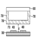
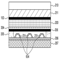
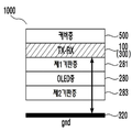
도3b는 본 발명의 실시예에 따라 터치 위치 및 터치 압력을 검출할 수 있도록 구성된 제2예의 터치 입력 장치의 단면도이다. 도3b에 예시된 터치 입력 장치(1000)의 단면도는 터치 입력 장치(1000)의 일부의 단면도일 수 있다. 도3b에 예시된 바와 같이, 본 발명의 실시예에 따른 터치 입력 장치(1000)는 디스플레이 패널(200A), 디스플레이 패널(200A) 하부에 배치된 백라이트 유닛(200B), 및 디스플레이 패널(200A) 상부에 배치된 커버층(500)을 포함하여 구성될 수 있다. 실시예에 따른 터치 입력 장치(1000)에서 압력 센서(450, 460)는 제1지지부재(240)상에 형성될 수 있다. 본 명세서에서 디스플레이 패널(200A) 및 백라이트 유닛(200B)을 포함하여, 디스플레이 모듈(200)로 지칭될 수 있다. 도3b에서 제1지지부재(240) 상에 압력 센서(450, 460)가 부착된 것이 예시되나, 실시예에 따라 제1지지부재(240)와 동일 및/또는 유사한 기능을 수행하는 터치 입력 장치(1000)에 포함된 구성에 부착되는 것도 가능하다. 3B is a cross-sectional view of a second example of a touch input device configured to detect a touch position and a touch pressure according to an embodiment of the present invention. The cross-sectional view of the
실시예에 따른 터치 입력 장치(1000)는 셀폰(cell phone), PDA(Personal Data Assistant), 스마트폰(smartphone), 태블랫 PC(tablet Personal Computer), MP3 플레이어, 노트북(notebook) 등과 같은 터치 스크린을 포함하는 전자 장치를 포함할 수 있다. The
실시예에 따른 터치 입력 장치(1000)에서 디스플레이 패널(200A)은 터치 센서 중 적어도 일부가 디스플레이 패널(200A) 내부에 포함되는 디스플레이 패널일 수 있다. 또한, 실시예에 따라 터치 센싱을 위한 구동전극 및 수신전극이 디스플레이 패널(200A) 내부에 포함될 수 있다. In the
실시예에 따른 커버층(500)은 디스플레이 패널(200A)의 전면을 보호하고 터치 표면을 형성하는 글라스(glass)로 구성될 수 있다. 커버층(500)은 디스플레이 패널(200A)을 보호하는 기능을 수행할 수 있다. 실시예에서 커버층(500)은 외부 환경으로부터 디스플레이 패널(200A)을 보호하면서도 디스플레이 화면이 시각적으로 확인될 수 있도록 투명한 물질로 구성될 수 있다. 예컨대, 커버층(500)은 유리 또는 플라스틱(plastic)과 같은 물질로 구성될 수 있으며 실시예에 따라 유리/플라스틱 외의 다른 물질로 구성되는 것도 가능하다. 도3b에 예시된 바와 같이, 커버층(500)은 디스플레이 패널(200A)보다 넓게 형성될 수 있다. The
실시예에 따른 LCD 패널과 같은 디스플레이 패널(200A)은 그 자체로 발광하지 못하고 다만 빛을 차단 내지 투과시키는 기능을 수행하므로 백라이트 유닛(backlight unit: 200B)이 요구될 수 있다. 예컨대, 백라이트 유닛(200B)은 디스플레이 패널(200A)의 하부에 위치하고 광원을 포함하여 디스플레이 패널(200A)에 빛을 비추어 화면에는 밝음과 어두움뿐 아니라 여러 가지 다양한 색상을 갖는 정보를 표현하게 된다. 디스플레이 패널(200A)은 수동소자로서 자체 발광하지 못하므로, 후면에 균일한 휘도 분포를 갖는 광원이 요구되는 것이다.The backlight unit 200B may be required because the
실시예에 따른 백라이트 유닛(200B)은 디스플레이 패널(200A)에 빛을 비추도록 하기 위한 광학층(220)을 포함하여 구성될 수 있다. 광학층(220)에 대해서는 도3c를 참조하여 상세히 살펴본다. The backlight unit 200B according to the embodiment may include an
실시예에 따른 백라이트 유닛(200B)은 제1지지부재(240)를 포함하여 구성될 수 있다. 제1지지부재(240)는 메탈(metal)로 구성된 프레임(frame)일 수 있다. 터치 입력 장치(1000)의 커버층(500)을 통해 외부에서 압력이 인가되는 경우, 커버층(500) 및 디스플레이 모듈(200) 등이 휘어질 수 있다. 이때, 휘어짐을 통해 압력 센서(450, 460)와 디스플레이 모듈 내부에 위치하는 기준 전위층 사이의 거리가 변화하고, 이러한 거리 변화에 따른 정전 용량 변화를 압력 센서(450, 460)를 통해 검출함으로써 압력의 크기를 검출할 수 있다. 이때, 압력의 크기를 정밀하게 검출하기 위해서 커버층(500)에 대해 압력을 인가하는 경우 압력 센서(450, 460)의 위치는 변하지 않고 고정될 필요가 있다. 따라서, 제1지지부재(240)는 압력의 인가에도 커버층(500) 및/또는 디스플레이 패널(200A) 등에 비해 덜 휘어지고 압력 센서를 고정시킬 수 있는 지지부 역할을 수행할 수 있다. 실시예에 따라 제1지지부재(240)는 백라이트 유닛(200B)과 별개로 제작되어 디스플레이 모듈 제작 시에 함께 조립될 수 있다. The backlight unit 200B according to the embodiment may include the
실시예에 따른 터치 입력 장치(1000)에서 디스플레이 패널(200A)과 백라이트 유닛(200B) 사이는 제1에어갭(210: air gap)을 포함하여 구성될 수 있다. 이는 디스플레이 패널(200A) 및/또는 백라이트 유닛(200B)을 외부의 충격으로부터 보호하기 위함이다. 이러한 제1에어갭(310)은 백라이트 유닛(200B)에 포함되도록 구성될 수 있다. In the
백라이트 유닛(200B)에 포함되는 광학층(220)과 제1지지부재(240) 사이는 서로 이격되도록 구성될 수 있다. 광학층(220)과 제1지지부재(240) 사이는 제2에어갭(230)으로 구성될 수 있다. 제1지지부재(240) 상에 배치된 압력 센서(450, 460)가 광학층(220)에 접촉하지 않는 것을 보장하고, 커버층(500)에 외부 압력이 인가되어 광학층(220), 디스플레이 패널(200A) 및 커버층(500)이 휘어지더라도 광학층(220)과 압력 센서(450, 460)가 접촉하여 광학층(220)의 성능을 저하시키는 것을 방지하기 위해서 제2에어갭(230)이 요구될 수 있다. The
실시예에 따른 터치 입력 장치(1000)는 디스플레이 패널(200A), 백라이트 유닛(200B) 및 커버층(500)이 결합되어 고정된 형태를 유지할 수 있도록 제2지지부재(251, 252)를 더 포함할 수 있다. 실시예에 따라, 제1지지부재(240)는 제2지지부재(251, 252)와 일체로 형성될 수 있다. 실시예에 따라 제2지지부재(251, 252)는 백라이트 유닛(200B)의 일부를 형성할 수 있다.The
LCD 패널(200A) 및 백라이트 유닛(200B)의 구조 및 기능은 공지된 기술이며 이하에서 간단히 살펴본다. 백라이트 유닛(200B)은 수개의 광학적 부품(optical part)을 포함할 수 있다.The structures and functions of the
도3c는 실시예에 따른 터치 입력 장치에서 백라이트 유닛(200B)의 광학층(220)을 예시한다. 도3c에서는 디스플레이 패널(200A)로서 LCD 패널을 이용하는 경우의 광학층(220)을 예시한다. 3C illustrates the
도3c에서 백라이트 유닛(200B)의 광학층(220)은 반사시트(221), 도광판(222), 확산시트(223) 및 프리즘시트(224)를 포함할 수 있다. 이때, 백라이트 유닛(200B)은 선광원(linear light source) 또는 점광원(point light source)등의 형태로서 도광판(222)의 후면 및/또는 측면에 배치된 광원(미도시)을 포함할 수 있다.3C, the
도광판(222: light guide plate)은 일반적으로 선광원 또는 점광원의 형태인 광원(미도시)으로부터 광들을 면광원 형태로 변환하여 LCD 패널(200A)로 향하게 하는 역할을 할 수 있다. The light guide plate 222 may function to convert light from a light source (not shown) in the form of a linear light source or a point light source to a surface light source and direct the light to the
도광판(222)에서 방출되는 광의 일부가 LCD 패널(200A)의 반대편으로 방출되어 손실될 수 있다. 반사시트(221)은 이러한 손실된 광을 도광판(222)으로 재입사 시킬 수 있도록 도광판(222) 하부에 위치하며 반사율이 높은 물질로 구성될 수 있다. A part of the light emitted from the light guide plate 222 may be emitted to the opposite side of the
확산시트(223: diffuser sheet)는 도광판(222)으로부터 입사되는 광을 확산시키는 역할을 한다. 예컨대, 도광판(222)의 패턴(pattern)에 의하여 산란된 빛은 직접 눈으로 들어오기 때문에 도광판(222)의 패턴이 그대로 비치게 될 수 있다. 심지어 이러한 패턴은 LCD 패널(200A)을 장착한 후에도 확연하게 감지할 수 있으므로 확산시트(224)는 이러한 도광판(222)의 패턴을 상쇄시키는 역할을 수행할 수 있다. The diffuser sheet 223 serves to diffuse light incident from the light guide plate 222. For example, since the light scattered by the pattern of the light guide plate 222 enters directly into the eye, the pattern of the light guide plate 222 can be illuminated as it is. Even when the
확산시트(223)를 지나면 광 휘도는 급격히 떨어지게 된다. 따라서, 광을 다시 포커스(focus)시켜 광 휘도를 향상시키도록 프리즘시트(224: prism sheet)가 포함될 수 있다. 프리즘시트(224)는 예컨대 수평 프리즘시트와 수직 프리즘 시트를 포함하여 구성될 수 있다. The light luminance rapidly drops after passing through the diffusion sheet 223. [ Thus, a prism sheet 224 (prism sheet) can be included to refocus the light to improve light brightness. The
실시예에 따른 백라이트 유닛(200B)은 기술의 변화, 발전 및/또는 실시예에 따라 전술한 구성과 다른 구성을 포함할 수 있으며, 또한 전술한 구성 이외에 추가적인 구성을 더 포함할 수 있다. 또한, 실시예에 따른 백라이트 유닛(200B)은 예컨대, 백라이트 유닛(200B)의 광학적 구성을 외부의 충격이나 이물 유입에 따른 오염 등으로부터 보호하기 위해서 보호 시트(protection sheet)를 프리즘 시트(224) 상부에 더 포함할 수 있다. 또한, 백라이트 유닛(200B)은 광원으로부터의 광 손실을 최소화하기 위해서 실시예에 따라 램프 커버(lamp cover)를 더 포함할 수 있다. 또한, 백라이트 유닛(200B)은 백라이트 유닛(200B)의 주요 구성인 도광판(222), 확산시트(223), 프리즘시트(224) 및 램프(미도시) 등이 허용치수에 맞게 정확하게 형합이 가능하도록 하는 형태를 유지하게 해주는 프레임(frame)을 더 포함할 수도 있다. 또한, 전술한 구성 각각은 2개 이상의 별개의 부분으로 이루어질 수 있다. The backlight unit 200B according to the embodiment may include other configurations than those described above according to changes, developments, and / or embodiments of the technology, and may further include additional configurations in addition to the configurations described above. The backlight unit 200B according to the embodiment may further include a protection sheet on the upper side of the
실시예에 따라, 도광판(222)과 반사시트(221) 사이에는 추가의 에어갭이 존재하도록 구성될 수 있다. 이에 따라 도광판(222)으로부터 반사시트(221)로의 손실광이 반사시트(221)를 통해 다시 도광판(222)으로 재입사될 수 있다. 이때, 상기 추가의 에어갭을 유지할 수 있도록 도광판(222)과 반사판(221) 사이로서 가장자리에는 양면 접착 테이프(DAT: Double Adhesive Tape)가 포함될 수 있다. 또한 실시예에 따라 임의의 다른 고정부재를 통해 도광판(222)과 반사판(221)이 서로 이격되어 배치될 수 있다. According to the embodiment, an additional air gap may be provided between the light guide plate 222 and the
이상에서 살펴본 바와 같이, 백라이트 유닛(200B) 및 이를 포함하는 디스플레이 모듈은 자체적으로 제1에어갭(210) 및/또는 제2에어갭(230)과 같은 에어갭을 포함하여 구성될 수 있다. 또는 광학층(220)에 포함된 복수의 층들 사이에 에어갭이 포함될 수 있다. 이상에서는 LCD 패널(200A)을 이용하는 경우에 대해서 설명하였으나, 다른 디스플레이 패널의 경우에도 구조 내에 에어갭을 포함할 수 있다. As described above, the backlight unit 200B and the display module including the backlight unit 200B may include air gaps such as the
도3d는 본 발명의 실시예에 따라 터치 위치 및 터치 압력을 검출할 수 있도록 구성된 제3예의 터치 입력 장치의 단면도이다. 도3d에서는 디스플레이 모듈(200)뿐 아니라 기판(300)을 더 포함하는 터치 입력 장치(1000)의 단면을 예시한다. 실시예에 따른 터치 입력 장치(1000)에서 기판(300)은, 예컨대 터치 입력 장치(1000)의 최외곽 기구인 제2커버(320)와 함께 터치 입력 장치(1000)의 작동을 위한 회로기판 및/또는 배터리가 위치할 수 있는 실장공간(310) 등을 감싸는 하우징(housing)의 기능을 수행할 수 있다. 이때, 터치 입력 장치(1000)의 작동을 위한 회로기판에는 메인보드(main board)로서 중앙 처리 유닛인 CPU(central processing unit) 또는 AP(application processor) 등이 실장되어 있을 수 있다. 기판(300)을 통해 디스플레이 모듈(200)과 터치 입력 장치(1000)의 작동을 위한 회로기판 및/또는 배터리가 분리되고, 디스플레이 모듈(200)에서 발생하는 전기적 노이즈가 차단될 수 있다. 실시예에 따라 기판(300)은 터치 입력 장치(1000)에서 미드 프레임(mid-frame)으로 지칭될 수 있다. FIG. 3D is a sectional view of a touch input device of a third example configured to detect a touch position and a touch pressure according to an embodiment of the present invention. 3D illustrates a cross-section of a
도3e에 예시된 바와 같이, 터치 입력 장치(1000)에서 커버층(500)이 디스플레이 모듈(200), 기판(300), 및 실장공간(310)보다 넓게 형성될 수 있으며, 이에 따라 제2커버(320)가 디스플레이 모듈(200), 기판(300) 및 회로기판이 위치하는 실장공간(310)을 감싸도록, 제2커버(320)가 형성될 수 있다.The
실시예에 따른 터치 입력 장치(1000)는 터치 센서 패널(100)을 통해 터치 위치를 검출하고, 디스플레이 모듈(200)과 기판(300) 사이에 압력 검출 모듈(400)을 포함할 수 있다. The
이때, 압력 검출 모듈(400)에 포함되는 압력 센서는 기판(300)상에 형성될 수도 있고, 디스플레이 모듈(200)상에 형성될 수도 있고, 디스플레이 모듈(200) 및 기판(300)상에 형성될 수도 있다. 또한, 압력 검출 모듈(400)에 포함되는 압력 센서를 구성하는 전극(450, 460)은 해당 전극을 포함하는 전극 시트(440)의 형태로 터치 입력 장치(1000)에 포함될 수 있으며, 이에 대해서는 이하에서 상세하게 살펴본다. The pressure sensor included in the
도3b 및 도3d에 예시된 바와 같이, 터치 입력 장치(1000)에서 압력 검출 모듈(400)은 디스플레이 모듈(200)과 기판(300) 사이에서 디스플레이 모듈(200) 하부에 배치되므로, 압력 검출 모듈(400)에 포함된 압력 센서를 구성하는 전극은 투명 물질뿐 아니라 불투명 물질로 구성되는 것도 가능하다.The
이하에서 본 발명의 실시예에 따른 터치 입력 장치(1000)에 압력 센서(450, 460)를 이용하여 터치 압력의 크기를 검출하는 원리 및 구조에 대해서 상세히 살펴본다. Hereinafter, the principle and structure for detecting the magnitude of the touch pressure using the
도4a 및 도4b는 터치 입력 장치에 포함된 제1예의 압력 센서와 기준 전위층 사이의 상대적인 거리 및 이에 압력이 인가된 경우를 예시한다.4A and 4B illustrate the relative distance between the pressure sensor of the first example included in the touch input device and the reference potential layer and the case where the pressure is applied thereto.
본 발명의 실시예에 따른 터치 입력 장치(1000)에서 압력 센서(450, 460)는 백라이트 유닛(200B)을 구성할 수 있는 제1지지부재(240) 상에 부착될 수 있다. 터치 입력 장치(1000)에서 압력 센서(450, 460)와 기준 전위층(600)은 거리(d)로 이격되어 위치할 수 있다. The
도4a에서 기준 전위층(600)과 압력 센서(450, 460) 사이는 스페이서층(미도시)을 사이에 두고 이격될 수 있다. 이때, 스페이서층은 도3b 및 도3c를 참조하여 설명된 바와 같이 디스플레이 모듈(200) 및/또는 백라이트 유닛(200B)의 제조시에 포함되는 제1에어갭(210), 제2에어갭(230) 및/또는 추가의 에어갭일 수 있다. 디스플레이 모듈(200) 및/또는 백라이트 유닛(200A)이 하나의 에어갭을 포함하는 경우 해당 하나의 에어갭이 스페이서층의 기능을 수행할 수 있으며, 복수 개의 에어갭을 포함하는 경우 해당 복수개의 에어갭이 통합적으로 스페이서층의 기능을 수행할 수 있다. In FIG. 4A, the reference
실시예에 따른 터치 입력 장치(1000)에서 스페이서층은 기준 전위층(600)과 압력 센서(450, 460) 사이에 위치할 수 있다. 이에 따라, 커버층(500)에 대해서 압력이 인가된 때 기준 전위층(600)이 휘어져 기준 전위층(600)과 압력 센서(450, 460) 사이의 상대적인 거리가 감소할 수 있다. In the
실시예에 따른 터치 입력 장치(1000)에서, 디스플레이 모듈(200)은 압력을 인가하는 터치에 따라 휘어지거나 눌릴 수 있다. 디스플레이 모듈은 터치의 위치에서 가장 큰 변형을 나타내도록 휘어지거나 눌릴 수 있다. 실시예에 따라 디스플레이 모듈이 휘어지거나 눌릴 때 가장 큰 변형을 나타내는 위치는 상기 터치 위치와 일치하지 않을 수 있으나, 디스플레이 모듈은 적어도 상기 터치에 따라 휘어짐 또는 눌림을 나타낼 수 있다. 예컨대, 터치 위치가 디스플레이 모듈의 테두리 및 가장자리 등에 근접하는 경우 디스플레이 모듈이 휘어지거나 눌리는 정도가 가장 큰 위치는 터치 위치와 다를 수 있다. In the
실시예에 따른 터치 입력 장치(1000)에 대한 터치시 커버층(500), 디스플레이 패널(200A), 및/또는 백라이트 유닛(200B)이 휘어지거나 눌릴 때 도4b에 도시된 바와 같이 스페이서층으로 인해 스페이서층 하부에 위치한 제1지지부재(240)는 휘어짐이나 눌림이 감소될 수 있다. 도4b에서는 제1지지부재(240)의 휘어짐 또는 눌림이 전혀 없는 것으로 도시되었으나 이는 예시일 뿐이며 압력 센서(450, 460)가 부착된 제1지지부재(240)의 최하부에서도 휘어짐 또는 눌림이 있을 수 있으나 스페이서층을 통해 그 정도가 완화될 수 있다. When the
실시예에 따라 스페이서층은 에어갭(air gap)으로 구현될 수 있다. 스페이서층은 실시예에 따라 충격흡수물질로 이루어질 수 있다. 스페이서층은 실시예에 따라 유전 물질(dielectric material)로 채워질 수 있다Depending on the embodiment, the spacer layer may be implemented with an air gap. The spacer layer may be made of a shock-absorbing material according to an embodiment. The spacer layer may be filled with a dielectric material according to embodiments
도4b는 도4a의 구조에서 압력이 인가된 경우를 예시한다. 예컨대, 도3b에 예시된 커버층(500)에 외부 압력이 인가된 경우에 기준 전위층(600)과 압력 센서(450, 460) 사이에 상대적인 거리가 d에서 d'로 감소함을 알 수 있다. 따라서, 실시예에 따른 터치 입력 장치(1000)에서 외부 압력이 인가된 경우에 기준 전위층(600)을 압력 센서(450, 460)가 부착된 제1지지부재(240)에 비해서 더 휘어지도록 구성함으로써 터치 압력의 크기를 검출할 수 있다.FIG. 4B illustrates a case where pressure is applied in the structure of FIG. 4A. For example, when external pressure is applied to the
도3b, 도4a 및 도4b에서 압력 검출을 위한 압력 센서(450, 460)로서 제1전극(450) 및 제2전극(460)을 포함하는 경우가 예시된다. 이때, 제1전극(450)과 제2전극(460) 사이에는 상호 정전용량(mutual capacitance)이 생성될 수 있다. 이때, 제1전극(450)과 제2전극(460) 중 어느 하나는 구동전극일 수 있고 나머지 하나는 수신전극일 수 있다. 구동전극에 구동신호를 인가하고 수신전극을 통해 감지신호를 획득할 수 있다. 전압이 인가되면, 제1전극(450)과 제2전극(460) 사이에 상호 정전용량이 생성될 수 있다.3B, 4A and 4B illustrate the case where the first and
기준 전위층(600)은 제1전극(450)과 제2전극(460) 사이에 생성된 상호 정전용량에 변화를 야기할 수 있도록 하는 임의의 전위를 가질 수 있다. 예컨대, 기준 전위층(600)은 그라운드(ground) 전위를 갖는 그라운드 층일 수 있다. 기준 전위층(600)은 디스플레이 모듈 내에 포함되는 임의의 그라운드(ground) 층일 수 있다. 실시예에 따라 기준 전위층(600)은 터치 입력 장치(1000)의 제조시에 자체적으로 포함되는 그라운드 전위층일 수 있다. 예컨대, 도2a 내지 도2c에 도시된 디스플레이 패널(200)에서 제1편광층(271)과 제1기판층(261) 사이에 노이즈(noise) 차폐를 위한 전극(미도시)을 포함할 수 있다. 이러한 차폐를 위한 전극은 ITO로 구성될 수 있으며 그라운드 역할을 수행할 수 있다. 또한, 실시예에 따라 기준 전위층(600)은 디스플레이 패널(200)에 포함되는 복수의 공통 전극이 기준 전위층을 구성할 수 있다. 이때 공통 전극의 전위가 기준 전위일 수 있다. The reference
커버층(500)에 대해서 객체로 터치시 압력이 가해진 경우 커버층(500), 디스플레이 패널(200A) 및/또는 백라이트 유닛(200B)의 적어도 일부가 휘어지므로 기준 전위층(600)과 제1전극(450) 및 제2전극(460) 사이의 상대적인 거리가 d에서 d'로 가까워질 수 있다. 이때, 기준 전위층(600)과 제1전극(450) 및 제2전극(450) 사이의 거리가 가까워질수록, 제1전극(450)과 제2전극(460) 사이의 상호 정전용량의 값은 감소할 수 있다. 기준 전위층(600)과 제1전극(450) 및 제2전극(460) 사이의 거리가 d에서 d'로 감소함으로써 상기 상호 정전용량의 프린징 정전용량이 객체뿐 아니라 기준 전위층(600)으로도 흡수되기 때문이다. 터치 객체가 부도체인 경우에는 상호 정전용량의 변화는 단순히 기준 전위층(600)과 전극(450, 460) 사이의 거리 변화(d-d')에만 기인할 수 있다. At least a part of the
이상에서는 압력 센서(450, 460)로서 제1전극(450)과 제2전극(460)을 포함하고, 이 둘 사이의 상호 정전용량의 변화로부터 압력을 검출하는 경우를 설명하였다. 압력 센서(450, 460)는 제1전극(450)과 제2전극(460) 중 어느 하나(예컨대, 제1전극(450))만을 포함하도록 구성될 수 있다. The case where the first and
도4c 및 도4d는 터치 입력 장치에 포함된 제2예의 압력 센서와 기준 전위층 사이의 상대적인 거리 및 이에 압력이 인가된 경우를 예시한다. 이때, 제1전극(450)과 기준 전위층(600) 사이의 자기 정전용량(self capacitance)을 검출함으로써 터치 압력의 크기를 검출할 수 있다. 이때, 제1전극(450)에 구동신호가 인가되고 제1전극(450)으로부터 수신신호를 입력받아 제1전극(450)과 기준 전위층(600) 사이의 자기 정전용량 변화를 검출함으로써 터치 압력의 크기가 검출될 수 있다. 4C and 4D illustrate the relative distance between the pressure sensor of the second example included in the touch input device and the reference potential layer and the case where the pressure is applied thereto. At this time, the magnitude of the touch pressure can be detected by detecting the self capacitance between the
예컨대, 기준 전위층(600)과 제1전극(450) 사이의 거리 변화에 따라 야기되는 제1전극(450)과 기준 전위층(600) 사이의 정전용량 변화로부터 터치 압력의 크기를 검출할 수 있다. 터치 압력이 커짐에 따라 거리(d)가 감소하므로 기준 전위층(600)과 제1전극(450) 사이의 정전용량은 터치 압력이 증가할수록 커질 수 있다.For example, it is possible to detect the magnitude of the touch pressure from the capacitance change between the
실시예에 따라, 터치 압력의 크기가 충분히 큰 경우 소정 위치에서 기준 전위층(600)과 압력 센서(450, 460) 사이의 거리가 더 이상 가까워지지 않는 상태에 다다를 수 있다. 이러한 상태를 이하에서는 포화 상태라고 지칭한다. 하지만, 이러한 경우에도 터치 압력의 크기가 더 커지는 때에는 기준 전위층(600)과 압력 센서(450, 460) 사이의 거리가 더 이상 가까워지지 않는 포화 상태에 있는 면적이 커질 수 있다. 이러한 면적이 커질수록 제1전극(450)과 제2전극(460) 사이의 상호 정전용량은 감소할 수 있다. 이하에서 거리의 변화에 따른 정전용량 변화에 따라서 터치 압력의 크기를 산출하는 것이 설명되나 이는 포화 상태에 있는 면적의 변화에 따라서 터치 압력의 크기를 산출하는 것을 포함할 수 있다. 이는 도4e와 관련된 실시예에도 적용될 수 있다. According to the embodiment, when the magnitude of the touch pressure is sufficiently large, the distance between the reference
도3b, 도4a 내지 도4d에서 제1전극(450) 및/또는 제2전극(460)의 두께가 상대적으로 두껍게 도시되고 이들이 직접 제1지지부재(240)에 부착된 것이 도시되나, 이는 설명의 편의를 위한 것이며 실시예에 따라 제1전극(450) 및/또는 제2전극(460)은 예컨대 일체형 시트(sheet)의 형태로 커버(240)에 부착될 수 있으며 상대적으로 그 두께가 작을 수 있다.The thickness of the
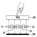
이상에서는 도3b에 예시된 터치 입력 장치(1000)를 참조하여 압력 센서(450, 460)가 제1지지부재(240)에 부착된 경우에 대해서 설명하였으나, 압력 센서(450, 460)는 도3d 및 도3e에 예시된 터치 입력 장치(1000)에서 디스플레이 모듈(200)과 기판(300) 사이에 배치될 수 있다. 실시예에 따라, 압력 센서(450, 460)가 디스플레이 모듈(200) 하부에 부착될 수 있으며, 이 경우, 기준 전위층(600)은 기판(300)이거나, 또는 디스플레이 모듈(200) 내부에 위치하는 임의의 전위층일 수 있다. 또한, 실시예에 따라 압력 센서(450, 460)가 기판(300)에 부착될 수 있으며, 이 경우, 기준 전위층(600)은 디스플레이 모듈(200) 또는 디스플레이 모듈(200) 내부에 위치하는 임의의 전위층일 수 있다. The
도4e는 터치 입력 장치에 포함된 제3예의 압력 센서의 배치를 예시한다. 도4e에 예시된 바와 같이, 압력 센서(450, 460) 중 제1전극(450)은 기판(300) 상에 배치되고 제2전극(460)은 디스플레이 모듈(200) 하부에 배치될 수 있다. 이 경우, 별도의 기준 전위층이 요구되지 않을 수 있다. 터치 입력 장치(1000)에 대해 압력 터치가 수행되는 경우, 디스플레이 모듈(200)과 기판(300) 사이의 거리가 변할 수 있고 이에 따라 제1전극(450)과 제2전극(460) 사이의 상호 정전용량이 증가할 수 있다. 이러한 정전용량 변화로부터 터치 압력의 크기를 검출할 수 있다. 4E illustrates the arrangement of the third example pressure sensor included in the touch input device. The
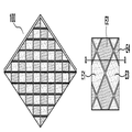
도5a 내지 도5e는 본 발명에 따른 압력 센서를 구성하는 전극의 제1예 내지 제5예에 따른 패턴을 예시한다. 5A to 5E illustrate a pattern according to the first to fifth examples of the electrodes constituting the pressure sensor according to the present invention.
도5a에서는 제1전극(450)과 제2전극(460) 사이의 상호 정전용량의 변화를 통해 터치 압력을 검출하는 경우의 압력 전극의 제1예에 따른 패턴이 예시된다. 제1전극(450)과 제2전극(460) 사이의 상호 정전용량이 변화함에 따라 터치 압력의 크기를 검출할 때, 검출 정확도를 높이기 위해서 필요한 정전용량 범위를 생성하도록 제1전극(450)과 제2전극(460)의 패턴을 형성할 필요가 있다. 제1전극(450)과 제2전극(460)이 서로 마주하는 면적이 크거나 길이가 길수록 생성되는 정전용량의 크기가 커질 수 있다. 따라서, 필요한 정전용량 범위에 따라 제1전극(450)과 제2전극(460) 사이의 마주하는 면적의 크기, 길이 및 형상 등을 조절하여 설계할 수 있다. 도5a에서는 제1전극(450)과 제2전극(460)이 마주하는 길이가 길어지도록 빗살형상의 압력 전극 패턴이 예시된다. 5A illustrates a pattern according to the first example of the pressure electrode in the case where the touch pressure is detected through a change in mutual electrostatic capacitance between the
도5a에서는 압력 검출을 위한 제1전극(450)과 제2전극(460)이 하나의 채널을 형성하는 경우를 나타내나, 도5b에서는 압력 센서가 2개의 채널을 구성하는 경우의 패턴을 예시한다. 도5b에서 제1채널을 구성하는 제1전극(450-1)과 제2전극(460-1)과 제2채널을 구성하는 제1전극(450-2)과 제2전극(460-2)이 도시된다. 도5c에서는 제1전극(450)은 2개의 채널(450-1, 450-2)을 구성하나 제2전극(460)은 1개의 채널을 구성하는 경우가 예시된다. 압력 센서가 제1채널과 제2채널을 통해 서로 다른 위치에서 터치 압력의 크기가 검출될 수 있으므로 멀티 터치의 경우에도 각각의 터치에 대해서 터치 압력의 크기가 검출될 수 있다. 이때, 실시예에 따라 압력 센서(450, 460)는 더 많은 수의 채널을 형성하도록 구성될 수 있다. 5A illustrates a case where the
도5d에서는 기준 전위층(600)과 제1전극(450) 사이의 자기 정전용량의 변화에 따라 터치 압력의 크기를 검출하는 경우의 전극 패턴을 예시한다. 도5d에서 제1전극(450)으로서 빗살형상의 패턴이 예시되나, 제1전극(450)은 판형상(예컨대, 사각형, 원형 등)을 가질 수 있다. 5D illustrates an electrode pattern in the case where the magnitude of the touch pressure is detected in accordance with the change of the self-capacitance between the reference
도5e에서는 제1전극(451 내지 459) 각각이 9개의 채널을 구성하는 경우가 예시된다. 즉, 도5d에서는 1개의 채널을 구성하는 경우를 예시하며 도5e에서는 9개의 채널을 구성하는 경우의 압력 센서를 예시한다. 따라서, 도5e의 경우 멀티 터치의 경우에도 각각에 대한 터치 압력의 크기를 검출할 수 있다. 이때, 다른 개수의 채널을 구성하도록 압력 센서가 구성될 수 있다. In FIG. 5E, the case where each of the
본 발명의 실시예에서 압력 센서(450, 460)는 복수의 채널을 형성하는 복수의 전극을 포함할 수 있다. 또한, 본 발명의 실시예에서 복수의 채널을 이용하여 복수의 터치 압력을 검출할 수 있다. In an embodiment of the present invention, the
도6a는 실시예에 따른 터치 입력 장치에 부착하기 위한 압력 전극을 포함하는 예시적인 전극 시트의 단면도이다. 예컨대, 전극 시트(440)는 제1절연층(470)과 제2절연층(471) 사이에 전극층(441)을 포함할 수 있다. 전극층(441)은 제1전극(450) 및/또는 제2전극(460)을 포함할 수 있다. 이때, 제1절연층(470)과 제2절연층(471)은 폴리이미드(polyimide), 페트(Polyethylene Terephthalate, PET) 등과 같은 절연 물질일 수 있다. 전극층(441)에 포함된 제1전극(450)과 제2전극(460)은 구리(copper), 알루미늄(A1), 은(Ag) 등과 같은 물질을 포함할 수 있다. 전극 시트(440)의 제조 공정에 따라 전극층(441)과 제2절연층(471) 사이는 OCA(Optically Clear Adhesive)와 같은 접착제(미도시)로 접착될 수 있다. 또한, 실시예에 따라 압력 전극(450, 460)은, 제1절연층(470) 위에 압력 전극 패턴에 상응하는 관통 구멍을 갖는 마스크(mask)를 위치시킨 후 전도성 스프레이(spray)를 분사하거나, 전도성 물질을 인쇄하거나, 금속물질이 도포되어 있는 상태에서 에칭하여 형성될 수 있다. 6A is a cross-sectional view of an exemplary electrode sheet including a pressure electrode for attachment to a touch input device according to an embodiment. For example, the
실시예에 따른 터치 입력 장치(1000)에서 터치 압력을 검출할 수 있도록, 하나 이상의 압력 전극(450, 460)을 포함하는 일체형의 전극 시트(440)는 압력 센서로서 기판(300), 디스플레이 모듈(200) 또는 제1지지부재(240)와 스페이서층(420)을 사이에 두고 이격되도록 기판(300), 디스플레이 모듈(200) 또는 커버(240)에 부착될 수 있다. 전극 시트(440)의 부착 방법은 도6b 내지 6d를 참조하여 이하에서 설명되는 방법 이외에도 도3a 내지 도3d의 구조에 적용되어 압력을 검출할 수 있도록 다양한 방법에 따라 터치 입력 장치(1000)에 부착될 수 있다. The
도6b는 제1방법에 따라 전극 시트가 터치 입력 장치에 부착된 터치 입력 장치의 일부의 단면도이다. 도6b에서는 전극 시트(440)가 기판(300), 디스플레이 모듈(200) 또는 제1지지부재(240) 상에 부착된 것이 도시된다.6B is a cross-sectional view of a portion of the touch input device in which the electrode sheet is attached to the touch input device according to the first method. In FIG. 6B, it is shown that the
도6c에 도시된 바와 같이, 스페이서층(420)을 유지하기 위해서 전극 시트(440)의 테두리를 따라 소정 두께를 갖는 접착 테이프(430)가 형성될 수 있다. 도6c에서 접착 테이프(430)는 전극 시트(440)의 모든 테두리(예컨대, 4각형의 4면)에 형성된 것이 도시되나, 접착 테이프(430)는 전극 시트(440)의 테두리 중 적어도 일부(예컨대, 4각형의 3면)에만 형성될 수도 있다. 이때, 도6c에 도시된 바와 같이, 접착 테이프(430)는 압력 전극(450, 460)을 포함하는 영역에는 형성되지 않을 수 있다. 이에 따라, 전극 시트(440)가 접착 테이프(430)를 통해 기판(300) 또는 디스플레이 모듈(200)에 부착될 때 압력 전극(450, 460)이 기판(300) 또는 디스플레이 모듈(200)과 소정 거리 이격되어 있을 수 있다. 실시예에 따라, 접착 테이프(430)는 기판(300)의 상부면, 디스플레이 모듈(200)의 하부면, 또는 제1지지부재(240)의 표면 상에 형성될 수 있다. 또한, 접착 테이프(430)는 양면 접착 테이프일 수 있다. 도6c에서는 압력 전극(450, 460) 중 하나의 압력 전극만을 예시하고 있다. 실시예에 따라, 복수의 채널을 형성하는 전극이 하나의 전극 시트(440)에 포함되어 압력 센서를 구성할 수 있다. An
도6d는 제2방법에 따라 전극 시트(440)가 터치 입력 장치에 부착된 터치 입력 장치의 일부의 단면도이다. 도6d에서는 전극 시트(440)를 기판(300), 디스플레이 모듈(200) 또는 제1지지부재(240) 상에 위치시킨 후 접착 테이프(431)로 전극 시트(440)를 기판(300), 디스플레이 모듈(200) 또는 제1지지부재(240)에 고정시킬 수 있다. 이를 위해 접착 테이프(431)는 전극 시트(440)의 적어도 일부와 기판(300), 디스플레이 모듈(200) 또는 제1지지부재(240)의 적어도 일부에 접촉할 수 있다. 도6d에서는 접착 테이프(431)가 전극 시트(440)의 상부로부터 이어져 기판(300), 디스플레이 모듈(200) 또는 커버(240)의 노출 표면까지 이어지도록 도시된다. 이때, 접착 테이프(431)는 전극 시트(440)와 맞닿는 면 측에만 접착력이 있을 수 있다. 따라서, 도6d에서 접착 테이프(431)의 상부면은 접착력이 없을 수 있다.6D is a cross-sectional view of a portion of a touch input device in which an
도6d에 도시된 바와 같이, 전극 시트(440)를 접착 테이프(431)를 통해 기판(300), 디스플레이 모듈(200) 또는 제1지지부재(240)에 고정시키더라도 전극 시트(440)와 기판(300), 디스플레이 모듈(200) 또는 커버(240) 사이에는 소정의 공간, 즉 에어갭이 존재할 수 있다. 이는 전극 시트(440)와 기판(300), 디스플레이 모듈(200) 또는 제1지지부재(240) 사이가 직접 접착제로 부착된 것이 아니며 또한 전극 시트(440)는 패턴을 갖는 압력 전극(450, 460)을 포함하므로 전극 시트(440)의 표면은 편평하지 않을 수 있기 때문이다. 이러한, 도6d에서의 에어갭 또한 터치 압력을 검출하기 위한 스페이서층(420)으로서 기능할 수 있다.6D, even if the
이상에서는 본 발명의 실시예에 따라 터치 위치 및/또는 터치 압력의 검출이 가능한 터치 입력 장치(1000)에 대해서 살펴보았다. 이하에서는 본 발명의 실시예에 따라 압력 검출 감도를 높일 수 있는 터치 입력 장치에 대해서 살펴본다. The
본 발명의 실시예에 따른 터치 입력 장치(1000)는 터치 표면에 압력을 인가하여 터치할 때 공기의 흐름을 원활하게 하는 관통홀(740)이 형성된 중간 기구(700)를 포함할 수 있다. 이때, 관통홀(740)은 공기 흐름이 가능한 에어홀일 수 있다. The
도7a 내지 도7e는 본 발명의 실시예에 따른 터치 입력 장치에서 기준 전위층과 중간 기구(700) 사이의 배치 관계를 나타내는 제1예 내지 제5예를 예시한다. 7A to 7E illustrate the first to fifth examples showing the arrangement relationship between the reference potential layer and the
본 발명의 실시예에 따른 터치 입력 장치(100)에서 중간 기구(700)는, 터치 압력의 인가에 따라 기준 전위층(600)과 압력 센서(450, 460) 사이의 거리가 용이하게 변할 수 있도록, 공기 흐름이 가능한 관통홀을 포함하여 형성될 수 있다. 본 명세서에서 중간 기구(700)는 터치 입력 장치(100)의 최외곽 기구, 하우징(housing), 케이스 등의 내부에 위치하는 임의의 부재일 수 있다. The
도7a에 예시된 바와 같이, 본 발명의 실시예에 따른 중간 기구(700)는 커버층(500)과 결합하여 그 내부 공간에 기준 전위층(600) 및 압력 센서(450, 460)를 포함하도록 구성될 수 있다. 이는 예시일뿐이며 중간 기구(700)는 커버층(500) 이외에 다른 구성과 함께 기준 전위층(600) 및 압력 센서(450, 460)를 포함하는 내부 공간을 형성할 수 있다. 7A, an
도7a에서 기준 전위층(600)은 커버층(500)에 접하여 배치되는 것으로 도시되나 이는 단지 예시일 뿐이며, 중간 기구(700)와 커버층(500)으로 형성되는 내부 공간에 기준 전위층(600)이 배치되는 것으로 충분하다. 이와 마찬가지로, 도7a에서 압력 센서(450, 460)도 중간 기구(700)에 접하여 배치되는 것으로 도시되나 압력 센서(450, 460)는 중간 기구(700)에 접하여 배치될 필요는 없으며, 중간 기구(700)와 커버층(500)으로 형성되는 내부 공간에 압력 센서(450, 460)가 배치되는 것으로 충분하다. 7A, the reference
또한, 실시예에 따라, 도7b에 예시된 바와 같이, 본 발명의 실시예에 따른 중간 기구(700)는 기준 전위층(600)과 결합하여 그 내부 공간에 압력 센서(450, 460)를 포함하도록 구성될 수 있다. 이는 예시일 뿐이며 중간 기구(700)는 기준 전위층(600) 이외에, 기준 전위층(600)을 포함하는 구성 또는 기준 전위층(600)과 직접/간접적으로 부착된 구성과 함께 압력 센서(450, 460)를 포함하는 내부 공간을 형성할 수 있다. 7B, the
도7b에서 압력 센서(450, 460)는 중간 기구(700)에 접하여 배치되는 것으로 도시되나 압력 센서(450, 460)는 중간 기구(700)에 접하여 배치될 필요는 없으며, 중간 기구(700)와 기준 전위층(600)으로 형성되는 내부 공간에 압력 센서(450, 460)가 배치되는 것으로 충분하다.7B, the
도7a에서는 중간 기구(700)가 커버층(500)과 함께 형성하는 내부 공간에 기준 전위층(600)뿐 아니라 압력 센서(450, 460)가 포함되는 경우가 예시되나, 실시예에 따라 기준 전위층(600)과 압력 센서(450, 460) 중 어느 하나만 내부 공간에 포함될 수 있다. 예컨대, 압력 센서(450, 460)는 중간 기구(700)의 외부에 배치될 수도 있다. 이러한 경우에도 관통홀(740)을 통해 공기 흐름이 자유롭게 됨으로써 커버층(500)에 압력이 안가되면 기준 전위층(600)의 휘어짐이 용이하게 이루어질 수 있다. 7A shows a case where the
이와 마찬가지로, 도7b에서는 중간 기구(700)가 기준 전위층(600)과 함께 형성하는 내부 공간에 압력 센서(450, 460)가 포함되는 경우가 예시되나, 실시예에 따라 압력 센서(450, 460)는 중간 기구(700)의 외부에 배치될 수도 있다. 이러한 경우에도 관통홀(740)을 통해 공기 흐름이 자유롭게 됨으로써 커버층(500)에 압력이 안가되면 기준 전위층(600)의 휘어짐이 용이하게 이루어질 수 있다.7B illustrates a case in which the
또한, 실시예에 따라 압력이 인가된 때 기준 전위층(600)에 비해서 압력 센서(450, 460)가 부착된 부재의 휘어짐이 용이하도록 중간 기구(700)가 배치될 수 있다. Further, according to the embodiment, the
예컨대, 도7c에 예시된 바와 같이, 압력 센서(450, 460)와 기준 전위층(600)이 모두 중간 기구(700)의 외부 공간에 배치될 수 있다. 도7c에서 압력 센서(450, 460)는 중간 기구(700)의 외부면에 접하여 배치되는 것으로 예시되나 반드시 중간 기구(700)에 직접 접하여 부착되지 않을 수 있다. 다만, 터치 압력의 인가에 따라 기준 전위층(600)에 비해 압력 센서(450, 460)의 상대적인 거리 이동이 더 큰 위치에 배치될 수 있다. 도7c에서, 기준 전위층(600)는 중간 기구(700)의 외부 공간에 배치되되 압력 센서(450, 460)와 거리 d로 이격되어 배치될 수 있다. 이러한 경우에도 커버층(500)에 압력이 인가되면 커버층(500)과 함께 중간 기구(700)가 휘어져 압력 센서(450, 460)와 기준 전위층(600) 사이의 상대적인 거리가 변하되, 터치 해제시 관통홀(740)을 통해 공기 흐름이 자유롭게 됨으로써 중간 기구(700) 및 중간 기구(700)의 내부 공간에 배치된 구성들의 휘어짐이 빠르게 원상 복구될 수 있다. For example, as illustrated in Fig. 7C, both the
또한, 도7d에 예시된 바와 같이, 압력 센서(450, 460)가 중간 기구(700)의 외부 공간에 배치될 수 있다. 이때, 기준 전위층(600)은 중간 기구(700) 그 자체가 되거나 중간 기구(700)의 내부 공간에 포함될 수 있다. 또는 실시예에 따라 기준 전위층(600)은 터치 압력의 인가에 따라 압력 센서(450, 460)에 비해 상대적인 거리 이동이 더 큰 위치에 배치될 수 있다. 도7d에서 압력 센서(450, 460)는 기판(300) 상에 배치되는 것으로 예시되나 반드시 기판(300)에 직접 접하여 부착되지 않을 수 있다. 이러한 경우에도 커버층(500)에 압력이 인가되면 커버층(500)과 함께 중간 기구(700)가 휘어져 압력 센서(450, 460)와 기준 전위층(600) 사이의 상대적인 거리가 변하되, 터치 해제시 관통홀(740)을 통해 공기 흐름이 자유롭게 됨으로써 중간 기구(700) 및 중간 기구(700)의 내부 공간에 배치된 구성들의 휘어짐이 빠르게 원상 복구될 수 있다. 7 (d), the
또한, 도4e에 예시된 바와 같이 압력 센서(450, 460)가 배치되는 경우에는, 제1전극(450)이 부착되는 부재와 제2전극(460)이 부착되는 부재 중 적어도 하나의 휘어짐이 용이하도록 관통홀(740)이 형성된 중간 기구(700)가 배치될 수 있다. When the
또한, 도7e에 예시된 바와 같이, 압력 센서(450, 460)가 디스플레이 모듈(200) 또는 디스플레이 패널(200A)의 하부로서 중간 기구(700)의 내부 공간에 배치될 수 있다. 실시예에 따라, 압력 센서(450, 460)가 디스플레이 모듈(200) 또는 디스플레이 패널(200A)의 하부에 부착될 수 있다. 이때, 기준 전위층(600)은 중간 기구(700) 그 자체가 되거나 중간 기구(700)의 내부 공간에 포함될 수 있다.7E, the
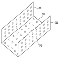
도7a 내지 도7e에 예시된 바와 같이, 중간 기구(700)는 하부 부재(710) 및 측면 부재(720, 730)가 일체형으로 형성될 수도 있으나, 실시예에 따라 하부 부재(710)와 측면 부재(720, 730)는 별개의 부재로서 서로 결합되어 중간 기구(700)를 형성할 수도 있다. 7A to 7E, the
이때, 본 발명의 실시예에 따른 터치 입력 장치(1000)에서 중간 기구(700)에는 도8a 내지 도8c에 예시된 바와 같이 관통홀(740)형성될 수 있다. 이는 터치 입력 장치(1000)의 터치 표면에 대한 터치시 압력 센서(450, 460)가 부착된 부재 및 기준 전위층(600) 중 적어도 하나의 휘어짐을 용이하게 하거나 휘어짐의 원상 복구를 용이하게 할 수 있다. In the
터치 입력 장치(1000)의 형체를 유지하고 내구성을 높이기 위해서, 터치 입력 장치(1000)를 구성하는 각 부재들은 빈틈없이 결속되어 일체가 되도록 결합할 수 있다. 이에 따라, 터치 입력 장치(1000)에 압력이 인가되는 경우에 공기 흐름이 자유롭지 않아 기준 전위층(600) 및/또는 압력 센서(450, 460)의 휘어짐이나 휘어짐의 복구가 용이하지 않을 수 있다. 즉, 터치 압력 검출의 정밀도를 높이기 위해서는, 터치 압력의 인가에 따라 눌림/휘어짐이 잘 일어나는 것에 더하여 압력이 해제된 후 빠르게 원상 복구될 필요가 있다. 공기의 흐름이 원활하지 않으면 이러한 원상 복구 시간이 지연될 수 있으며, 이러한 경우 후속되는 터치 압력의 검출시 오류가 발생할 수 있다. In order to maintain the shape of the
이에 따라 본 발명의 실시예에서는 터치 입력 장치(1000)에 포함된 중간 기구(700)에 관통홀(740)을 형성하여 공기가 중간 기구(700)를 관통하여 자유롭게 움직이도록 한다. 이에 따라 터치 압력의 인가에 따라 기준 전위층(600)과 압력 센서(450, 460) 사이의 거리가 제한되지 않으므로 압력 크기의 검출 정밀도가 향상될 수 있다. 또한, 그 휘어짐의 원상 복구가 빠르게 수행될 수 있으므로 후속 터치 검출을 저해하지 않을 수 있다. Accordingly, in the embodiment of the present invention, the through
관통홀(740)의 직경은 예컨대 수μm 정도일 수 있다. 또한, 실시예에 따라 관통홀(740)의 직경은 압력 터치시에 발생하는 기압 변화에 따라 공기의 유입/유출은 용이하되 직경 2.5μm 이상의 이물질은 통과할 수 없는 크기로 형성될 수 있다. The diameter of the through
도8a 내지 도8c는 본 발명의 실시예에 따른 터치 입력 장치에서 관통홀이 형성된 중간 기구의 제1예 내지 제3예를 예시한다. 도8a에 예시된 바와 같이, 관통홀(740)은 중간 기구(700)의 하부 부재(710)에 복수 개 형성될 수 있다. 또한, 실예에 따라 관통홀(740)은 균일하게 하부 부재(710)의 전체 면적에 걸쳐 형성될 수 있다. 8A to 8C illustrate first to third examples of an intermediate mechanism in which a through hole is formed in a touch input device according to an embodiment of the present invention. A plurality of through
압력 센서(450, 460) 또는 이를 포함하는 전극 시트(440)가 중간 기구(700)에 직접 부착되는 경우에, 전극 시트(440)로 인해 공기의 흐름이 방해받고 전극 시트(440)의 기능이 저하될 수 있다. 따라서, 도8b에 예시된 바와 같이 관통홀(740)은 중간 기구(700)의 하부 부재(710)에서 전극 시트(440)가 부착되지 않는 영역에만 형성될 수 있다. 이에 따라 전극 시트(440) 전체 면적에 대해 기준 전위층(600)과의 거리가 균일하게 유지될 수 있다. In the case where the
또한, 실시예에 따라 도8c에 예시된 바와 같이 중간 기구(700)의 하부 부재(710)뿐 아니라 측면 부재(720, 730)에도 관통홀(740)이 형성되어 공기의 흐름을 더욱 자유롭게 할 수 있다. 실시예에 따라 다양한 크기의 전극 시트(440)가 중간 기구(700)의 하부 부재(710)에 부착될 수 있도록 중간 기구(7100)의 측면 부재(720, 730)에만 관통홀(740)이 형성되어 있을 수 있다. 도8c에서는 중간 기구(700)의 측면 부재(720, 730)로서 두 측면 부재만이 예시되지만, 실시예에 따라 중간 기구(700)는 전체 측면에 따라 형성된 측면 부재(720, 730)를 포함할 수 있다. 이때, 관통홀(740)은 측면 부재(720, 730)의 일부에만 형성될 수도 있다. 8C, a through
본 발명의 실시예에서 관통홀(740)이 형성되는 중간 기구(700)는 제2지지 부재(251, 252)와 결합되는 제1지지 부재(240)일 수 있다. 실시예에 따라 중간 기구(700)는 임의의 측면 부재와 결합되는 기판(300)일 수 있다. 실시예에 따라 중간 기구(700)는 터치 입력 장치(1000)에 포함되는 임의의 부재로서 터치 압력의 인가에 따라 기준 전위층(600)과 압력 센서(450, 460) 사이의 거리 변화를 용이하게 할 수 있도록 형성된 관통홀(740)을 포함할 수 있다. The
이상에서는 디스플레이 패널(200A) 외부에 압력 센서(450, 460)를 별도로 구비하는 경우에 대해서 설명하였다. 본 발명의 실시예는 압력 센서(450, 460)를 디스플레이 패널(200A) 내부에 구비하는 경우뿐 아니라 압력 센서(450, 460)를 별도로 구비하지 않고 디스플레이 패널(200A)에 포함된 기존의 전극을 압력 센서로 이용하는 경우에도 적용될 수 있다. 또한, 실시예에 따라 터치 센서(100)를 압력 센서로(450, 460)로 이용하는 경우에도 적용될 수 있다. In the foregoing, the case where the
도9a 내지 도9c는 압력 센서(450, 460) 및 터치 위치 검출을 위한 전극이 디스플레이 패널(200A) 내부에 위치하는 구조를 예시한다. 이하에서 터치 위치 및 터치 압력을 검출하는 원리는 이상에서 설명된 것과 동일/유사 하므로 중복되는 설명은 생략한다. 9A to 9C illustrate a structure in which the
예컨대, 도9a 내지 도9c에서, 본 발명의 일 실시예에 따른 디스플레이 패널(200A)은 제1편광층(201), 복수의 제2전극(R)이 형성된 제2전극층(152), 컬러필터를 구비하는 제1기판층(203), 액정셀(liquid crystal cell)을 포함하는 액정층(205), 복수의 기준전극(654), 복수의 제1전극(T)과 복수의 제3전극(C)이 형성된 제1/제3전극층(156), 제2기판층(207) 및 제2편광층(209)이 스택구조로 되어 있다. 이때, 제2전극층(152)과, 컬러필터를 구비하는 제1기판층(203)의 위치는 서로 바뀌어도 무방하다. 9A to 9C, a
도9a 내지 도9c에 예시된 실시예에 따른 디스플레이 패널(200A)은 액정표시장치(liquid crystal display; LCD)에 포함된 디스플레이 패널일 수 있고, 이때 PLS(Plane to Line Switching)방식, IPS(In Plane Switching)방식, VA(Vertical Alignment)방식 및 TN(Twisted Nematic)방식 중 어느 방식의 디스플레이 패널이어도 무방하다. 또한, 본 발명의 디스플레이 패널(200A)은 유기발광 표시장치(Organic Light Emitting Diode; OLED) 등에 포함된 디스플레이 패널일 수 있다.The
복수의 제2전극(R)은, 터치에 따라 변하는 정전용량에 대한 정보를 가진, 터치위치와 관련한 제1신호를 생성한다. 또한, 복수의 제3전극(C)은, 터치에 따라 변하는 정전용량에 대한 정보를 가진, 터치압력과 관련한 제2신호를 생성한다.The plurality of second electrodes R generate a first signal related to the touch position, which has information on the capacitance that varies with the touch. In addition, the plurality of third electrodes C generate a second signal related to the touch pressure, which has information on the capacitance that varies with the touch.
도9a 내지 도9c에서, 액정층(205)에는 기준전극(654)이 구비되어 있으며 기준전극(654)는 전술한 기준전위층(600)과 동일한 역할을 할 수 있다. 액정층(205)에 접하여 제1/제3전극층(156)이 형성되며, 제1/제3전극층(156)에 구비된 복수의 제1전극(T)과 복수의 제3전극(C) 사이에는 상호 정전용량(Cm)이 생성된다. 9A to 9C, the
기준전극(654)은, 도9a 내지 도9c에 예시된 바와 같이, 액정층(205) 내에서 제1/제3전극층(156)과 이격되어 구비될 수 있다. 기준전극(654)은, 액정층(205)에 구비되는 스페이서(270)의 일부 혹은 전체에 전도성 물질층을 형성함으로써 이루어질 수 있다. 제1/제3전극층(156)은 기준전극(654)이 구비된 층의 상부에 형성될 수도 있지만, 실시예에 따라, 기준전극(654)이 구비된 층의 하부에 형성될 수도 있다. The
제1/제3전극층(156)이 기준전극(654)이 구비된 층의 하부에 형성되는 경우, 객체가 디스플레이 패널(200A)의 터치표면을 터치할 때 압력이 가해지면, 기준전극(654)이 하방으로 이동하게 되므로, 제1/제3전극층(156)과 가까워진다. 따라서, 제1전극(T)과 제3전극(C) 사이의 상호 정전용량(Cm)이 변화(감소)하게 된다. 다만, 기준전극(154)이 플로팅 노드인 경우에는, 제1전극(T)과 제3전극(C) 사이의 상호 정전용량(Cm)이 증가할 수도 있다.When the first /
또한, 객체가 디스플레이 패널(200A)의 터치표면을 터치하는 경우, 제1/제3전극층(156)에 구비된 제1전극(T)과, 제2전극층(152)에 구비된 제2전극(R) 사이의 상호 정전용량(Cm)이 감소하게 된다.In addition, when the object touches the touch surface of the
마찬가지로, 제1/제3전극층(156)이 기준전극(654)이 구비된 층의 상부에 형성되는 경우에는, 객체가 디스플레이 패널(100)의 터치표면을 터치할 때 압력이 가해지면, 제1/제3전극층(156)이 하방으로 이동하게 되므로, 기준전극(654)과 가까워진다. 따라서, 제1전극(T)과 제3전극(C) 사이의 상호 정전용량(Cm)이 변화(감소)하게 된다. 다만, 기준전극(654)이 플로팅 노드인 경우에는, 제1전극(T)과 제3전극(C) 사이의 상호 정전용량(Cm)이 증가할 수도 있다.Likewise, when the first /
상기 상호 정전용량(Cm)의 변화에 기초하여, 터치위치와 터치압력을 검출할 수 있는 제1신호와 제2신호가 생성될 수 있다. 또한, 제2전극(R)과 제3전극(C)이 서로 다른 층에 배치됨으로써, 제1신호 및 제2신호가 동시에 생성될 수 있다.Based on the change of the mutual capacitance Cm, a first signal and a second signal capable of detecting the touch position and the touch pressure can be generated. In addition, since the second electrode R and the third electrode C are disposed in different layers, the first signal and the second signal can be simultaneously generated.
다만, 다른 실시예에서는, 제1전극(T)과 기준전극(654) 사이의 거리에 따른 자기 정전용량(self capacitance; Cs)의 변화에 따라 압력을 검출할 수도 있을 것이다. 즉, 제1전극(T)과 기준전극(154) 사이 혹은, 제3전극(C)과 기준전극(654) 사이의 자기 정전용량(Cs)의 변화에 의하여 압력을 검출할 수도 있을 것이다. However, in another embodiment, the pressure may be detected in accordance with a change in self capacitance (Cs) according to the distance between the first electrode T and the
복수의 제1전극, 복수의 제2전극 및 복수의 제3전극은, 투명 전도성 물질(예를 들면, 산화주석(SnO2) 및 산화인듐(In2O3) 등으로 이루어지는 ITO(Indium Tin Oxide) 또는 ATO(Antimony Tin Oxide)) 등으로 형성될 수 있다. The plurality of first electrodes, the plurality of second electrodes, and the plurality of third electrodes may be formed of a transparent conductive material (for example, ITO (Indium Tin Oxide), such as tin oxide (SnO 2 ) and indium oxide (In 2 O 3 ) ) Or ATO (Antimony Tin Oxide)).
도9a의 실시예에 따른 디스플레이 패널(200A)은 제1기판층(203) 위에 제2전극층(152)이 구비된 구성을 나타낸다. 도9a에서는 최상위의 커버층(113)과 이를 접착하기 위한 OCA(optically clear adhesive)층(211)이 예시되고, 컬러필터층(204)이 제1기판층(203)과 별도로 도시되고, TFT층(206)이 제2기판층(207)과 별도로 도시된다. The
이때, 기준전극(654)의 형성위치는, 디스플레이 패널(200A)의 표면터치에 의해 휨이 발생함에 따라, 제1/제3전극층(156)과 기준전극(654) 사이의 거리변화가 이루어지는 위치라면, 도9a에 도시된 액정층(205)의 상면이 아니어도 무방하다.At this time, the formation position of the
디스플레이 패널(200A)의 액정층(205)에는 간격을 확보하기 위한 스페이서가 구비될 수 있다. 상기 스페이서는, 액정층(205) 내에서 형성되어도 무방하고, 액정층(205) 위에 위치한 상부층에 형성되어 있어도 무방하다. 본 발명의 일 실시예에서, 기준전극(654)은 상기 스페이서에 ITO와 같은 전도성 물질(conductive material)을 형성함으로써 이루어질 수 있다. The
일 실시예에서, 기준전극(654)은 상기 스페이서의 전체가 아닌 일부에 전도성 물질을 형성함으로써 이루어질 수 있다. 또한, 상기 스페이서와 별도로, 전도성 물질의 기준전극(654)이 형성될 수 있다. 즉, 기준전극(654)은 제1/제3전극층(156)으로부터 이격되어, 상호 정전용량(Cm)을 변화시킬 수 있는 전극으로서 기능할 수 있으면, 어떠한 방식으로 구비되어도 무방하다.In one embodiment, the
도9b는 본 발명의 또 다른 실시예에 따른 디스플레이 패널(200A)의 층구조를 나타낸다. 도9a와 달리, 본 실시예에서는, 복수의 제2전극(R)을 구비하는 제2전극층(152)이 액정층(205)에 접촉하여 형성되어 있다. 그 외의 구성은, 도9a와 관련한 설명에서 이루어졌으므로, 생략하기로 한다. 9B shows a layer structure of a
도9a 및 도9b는 기준전극(654)이 구비된 액정층(205)을 사이에 두고, 제1/제3전극층(156)과 제2전극층(152)이 이격되어 있는 다양한 형태의 실시예를 나타낸다. 기준전극(654)을 포함하는 액정층(205)을 사이에 두고, 제1/제3전극층(156)과 제2전극층(152)이 이격되어 있는 구조라면, 제2전극층(152) 혹은 제1/제3전극층(156)이 도9a나 도9b에 도시된 바와 다르게 형성되어도 무방하다.9A and 9B show various embodiments in which the
한편, 도9c는, 도9a나 도9b의 실시예와 달리, 기준전극(654)이 제1/제3전극층(156)의 하부에 형성된 층구조를 보여준다. 도9c에 도시된 바와 같이, 디스플레이 패널(200A)의 기준전극(654)은, 제1/제3전극층(156)의 하부에 이격되어 형성된다. 이때, 기준전극(654)의 형성위치는, 디스플레이 패널(200A)의 표면터치에 의해 휨이 발생함에 따라, 제1/제3전극층(156)과 기준전극(654) 사이의 거리변화가 이루어지는 위치라면, 액정층(205) 내의 어느 위치에 형성되어도 무방하다. 9C shows a layer structure in which the
도9c의 실시예에서도, 간격을 확보하기 위한 스페이서(215)가 디스플레이 패널(200A)의 액정층(205)에 구비될 수 있다. 기준전극(654)은 제1/제3전극층(156)의 하부에 형성되며, 스페이서(215)에 ITO와 같은 전도성 물질을 형성함으로써 이루어질 수 있다. 물론, 기준전극(654)은 스페이서(215)의 전체가 아닌 일부에 전도성 물질을 형성함으로써 이루어질 수 있다. 9C, a
또한, 전도성 물질의 기준전극(654)이 스페이서(215)와는 별도로 형성될 수도 있다. 즉, 기준전극(654)은 제1/제3전극층(156)의 하방으로 이격되어, 상호 정전용량(Cm)을 변화시킬 수 있는 전극으로서 기능할 수 있으면, 어떠한 방식으로 구비되어도 무방하다.Also, a
도10a 및 도10b는 디스플레이 패널 내부의 구성을 압력 검출을 위한 전극으로 이용하는 구조를 예시한다. 10A and 10B illustrate a structure in which the structure inside the display panel is used as an electrode for pressure detection.
도10a에 도시된, 본 발명의 일 실시예에 따른 디스플레이 패널(200A)의 제2기판층(207) 상부에는 TFT층(206)이 형성되어 있다. TFT층(206)은 액정층(205)을 구동하기 위한 전기장(eletric field)을 생성하는데 필요한 전기적 구성요소들을 포함한다. 특히, TFT층(206)은 데이터 라인(data line), 게이트 라인(gate line), TFT, 공통 전극(common electrode) 및 화소 전극(pixel electrode) 등을 포함하는 다양한 층으로 이루어질 수 있다. 이들 전기적 구성요소들은, 제어된 전기장을 생성하여 액정층(205)에 위치한 액정들을 배향시키도록 작동할 수 있다. A
본 발명의 일 실시예에서, 복수의 제1전극 및 복수의 제3전극은 디스플레이 패널(200A)에 포함된 공통전극을 이용할 수 있다.In an embodiment of the present invention, the plurality of first electrodes and the plurality of third electrodes may use a common electrode included in the
도10a에 도시된 바와 같이, 본 발명의 일 실시예에 따른 디스플레이 패널(200A)에서는, 제1/제3전극층(156)의 상부에 위치한 스페이서(215)에 ITO와 같은 전도성 물질을 형성하여, 기준전극(654)으로 이용한다. 스페이서(215)는 액정층(205)에 구비되어 있다고 설명하였지만, 컬러필터층(204)이 구비된 제1기판층(203)에 형성될 수도 있다. 여기서, 터치압력 신호와 관련한 프린징 정전용량(C1)은 공통 전극을 이용하는 복수의 제1전극(T)과 기준전극(654) 사이에 형성되고, 프린징 정전용량(C2)은 공통 전극을 이용하는 복수의 제3전극(C)과 기준전극(654) 사이에 형성될 수 있다.10A, in a
도10a에 도시된 바와 같이, 본 발명의 일 실시예에 따른 디스플레이 패널(200A)에서, 객체가 터치표면을 터치할 때 압력이 인가되면, 기준전극(654)과 TFT층(206) 사이의 거리가 감소하고, 이에 따라 로우 공통 전극으로 이루어진 복수의 제1전극(T)과 제3전극(C)이, 기준전극(654)과의 거리가 가까워져, 상호 정전용량(Cm)이 변화(감소 혹은 증가)하게 된다. 이에 따라 생성된 제2신호에 의하여, 터치압력을 검출할 수 있게 된다.10A, in a
도10a의 실시예에 있어서, 제2전극층(152)은 제1기판층(203) 상부에 형성된 것으로 도시했으나, 도9b와 같이, 컬러필터층(204) 하부에 형성될 수 있다. 10A, the
한편, 도10b에 도시된 바와 같이, 본 발명의 일 실시예에 따른 디스플레이 패널(200A)에서는, 제1/제3전극층(156)의 하부에 위치하는 스페이서(215)에 ITO와 같은 전도성 물질을 형성하여, 기준전극(654)으로 이용할 수 있다. 10B, in the
이때, 제1/제3전극층(156)은 액정층(205)의 상부에 위치하는 공통전극을 이용할 수 있다. 스페이서(215)는 액정층(205)에 구비되어 있다고 설명하였지만, 화소 전극을 포함하는 TFT층(206) 상에 형성될 수도 있다. At this time, the first /
여기서, 터치압력 신호와 관련한 프린징 정전용량(C1)은 공통 전극을 이용하는 복수의 제1전극(T)과 기준전극(654) 사이에 형성되고, 프린징 정전용량(C2)은 공통 전극을 이용하는 복수의 제3전극(C)과 기준전극(654) 사이에 형성될 수 있다.Here, the fringing capacitance C1 related to the touch pressure signal is formed between the plurality of first electrodes T using the common electrode and the
도10b에 도시된 바와 같이, 본 발명의 일 실시예에 따른 디스플레이 패널(200A)에서, 객체가 터치표면을 터치할 때 압력이 인가되면, 공통 전극으로 이루어진 복수의 제1전극(T)과 제3전극(C)이, 기준전극(654) 쪽으로 이동하면서, 거리가 가까워짐에 따라, 상호 정전용량(Cm)이 변화(감소)한다. 이에 의해 생성된 제2신호에 의하여, 터치압력을 검출할 수 있게 된다.10B, in a
한편, 도10a 및 도10b에서, 기준전극(654)이 플로팅 노드인 경우에는, 제1전극(T)과 제3전극(C)이 기준전극(654)과 가까워지면서 상호 정전용량(Cm)이 증가할 수 있다. 즉, 기준전극(654)과 제1전극(T) 사이의 정전용량(C1) 및 기준전극(154)과 제3전극(C) 사이의 정전용량(C2)이 증가하고, 제1전극(T)과 제3전극(C) 사이의 상호 정전용량(Cm)의 일정 부분을 차지하는, 정전용량(C1 및 C2)의 직렬연결 정전용량도 증가하게 되므로, 전체 상호 정전용량(Cm)도 증가하게 된다.10A and 10B, when the
도10a 및 도10b의 구성에 의하면, 어떤 구동 방식의 액정표시장치에도 본 발명을 적용할 수 있다. 즉, 공통전극이 액정층(205)의 상부에 위치하는 구조의 액정표시장치에도 적용이 가능하고, 액정층(205)의 하부에 위치하는 구조의 액정표시장치에도 적용이 가능하다.According to the configurations of Figs. 10A and 10B, the present invention can be applied to a liquid crystal display device of any driving system. That is, the present invention is also applicable to a liquid crystal display device having a structure in which the common electrode is located above the
더욱 상세하게 설명하면, 공통전극(common electrode)이 액정층 하부에 위치하는 PLS방식이나 IPS방식의 액정표시장치에는, 도10a의 실시예에 따른 디스플레이 패널(200A)이 적용될 수 있고, 공통전극이 액정층 상부에 위치하는 VA방식이나 TN방식의 액정표시장치에는, 도10b의 실시예에 따른 디스플레이 패널(200A)이 적용될 수 있다. More specifically, a
예컨대, 디스플레이 패널(200A) 내에서 복수의 공통 전극은, 일정한 간격을 갖고 바둑판 형상으로 배열될 수 있다. 이때, 공통 전극을 그룹화시킴으로써, 각각 제1전극(T) 및 제3전극(C)으로 기능할 수 있게 된다. For example, a plurality of common electrodes in the
도10a 및 도10b에 예시된 디스플레이 패널(200A)은, 디스플레이 패널(200A)의 전기적 구성요소들을 본래의 목적대로 동작하도록 함으로써 디스플레이 패널(200A)로서 기능할 수 있다. 또한, 디스플레이 패널(200A)은, 디스플레이 모듈(200)의 전기적 구성요소들의 적어도 일부를 터치압력 및 위치감지를 위하여 동작하도록 함으로써 터치압력 감지 모듈로서 기능할 수 있다. 이때, 각각의 동작 모드(mode)는 시분할로 동작할 수 있다. 즉, 제1시간 구간에 디스플레이 패널(200A)은 디스플레이 모듈로서 작동하고, 제2시간 구간에 터치압력 및/또는 터치위치 감지(혹은 입력)장치로서 기능할 수 있다.The
도9a 내지 도10b에서는, 압력 검출을 위한 압력 센서(450, 460) 및 기준전위층(600)에 대응하는 구성이 모두 디스플레이 패널(200A) 내부에 위치하는 실시예에 대해서 살펴보았다. 이러한 디스플레이 패널(200A)을 이용하는 경우에도 관통홀(740)이 형성된 중간기구(700)를 이용하여 얻을 수 있는 효과를 마찬가지로 얻을 수 있다. In FIGS. 9A and 10B, the embodiments in which the
예컨대, 도7a에 예시된 바와 같이, 중간기구(700)와 커버층(500)으로 형성되는 내부공간에 도9a 내지 도10b와 관련하여 설명된 디스플레이 패널(200A)이 배치될 수 있다. 이때, 내부공간에 디스플레이 패널(200A)이 배치되기 때문에 압력 센서(450, 460) 및 기준전위층(600)이 추가로 포함될 필요는 없다. 또는, 도7b에 예시된 바와 같이 기준전위층(600)을 포함하는, 도9a 내지 도10b에 예시된 디스플레이 패널(200A)이 중간기구(700)와 함께 내부공간을 형성할 수 있다. 다만, 압력 센서(450, 460)가 추가로 내부 공간에 포함될 필요는 없다. For example, as illustrated in Fig. 7A, the
도9a 내지 도10b에서, 압력 검출을 위한 전극 이외에 터치 위치 검출을 위한 전극도 디스플레이 패널(200A)에 포함된 경우가 예시되나, 실시예에 따라 터치 위치 검출을 위한 전극은 디스플레이 패널(200A) 외부에 배치될 수도 있다. 9A and 10B illustrate a case where an electrode for touch position detection is included in the
또한, 도9a 내지 도10b에서, 압력 검출을 위한 기준전극(654)이 디스플레이 패널(200A)에 포함된 경우가 예시되나, 실시예에 따라 기준전극(654)은 디스플레이 패널(200A) 외부에 배치될 수도 있다.9A to 10B illustrate a case where the
도11a 내지 도11c는 추가의 압력 센서가 요구되지 않는 OLED 디스플레이 패널을 포함하는 터치 입력 장치의 구조를 예시한다. 도11a에서 제1기판층(281)와 커버층(500) 사이에 터치 센서(100)가 배치되는 것이 예시된다. 도11a에서 제1기판층(281) 상에 터치 센서(100)가 형성될 수 있으며, 이러한 터치 센서(100)는 압력 센서(450, 460)로 이용될 수 있다. 도11a에서는 터치 센서(100)와 기준 전위층(600)이 이격되어 배치되어 있다. Figures 11A-11C illustrate the structure of a touch input device including an OLED display panel where no additional pressure sensor is required. In FIG. 11A, it is exemplified that the
도11a에 예시된 바와 같은 본 발명의 실시예에서, 기준 전위층(600)과 터치 센서(100) 사이의 거리에 따라 변하는 터치 센서(100) 로부터 감지되는 상호 정전용량 또는 자기 정전용량을 통해 터치 압력의 크기가 검출될 수 있다. In the embodiment of the present invention as illustrated in FIG. 11A, when a touch is detected by the
또한, 도11a에 예시된 바와 같은 본 발명의 실시예에서, 터치 센서(100)로부터 검출되는 자기 정전용량 또는 상호 정전용량을 통해 터치 위치가 검출될 수 있다. In addition, in the embodiment of the present invention as illustrated in FIG. 11A, the touch position can be detected through the self capacitance or the mutual capacitance detected from the
도11b는 도11a에 예시된 실시예에 따른 터치 입력 장치에 포함될 수 있는 터치 센서(100)의 배열을 예시한다. 터치 센서(100)는 동일한 층에 배열된 복수개의 전극을 포함할 수 있다. 이때, 도11b의 우측에 도시된 바와 같이 터치 센서(100) 일부를 a-a선을 따라 자른 전극(E1, E2, E3, E4)이 도11c에 예시된다. FIG. 11B illustrates an arrangement of the
도11c는 도11b에 예시된 터치 센서 배열을 통해 터치 위치 및 터치 압력을 검출하는 원리를 설명하는 개념도이다. 도11c에 예시된 바와 같이, 터치 센서(100)에 포함된 각 전극(E1, E2, E3, E4)으로부터 기준 전위층(600)에 대한 자기 정전용량을 감지하여, 터치 위치를 검출할 수 있다. 또는, 구동전극(E1, E3)과 수신전극(E2, E4) 사이에 생성되는 상호 정전용량을 감지하여, 터치 위치를 검출할 수 있다. FIG. 11C is a conceptual diagram for explaining the principle of detecting the touch position and the touch pressure through the arrangement of the touch sensor illustrated in FIG. 11B. The touch position can be detected by sensing the self-capacitance of the reference
또한, 도11c를 참조하여, 터치 센서(100)에 포함된 전극 중 적어도 하나 이상의 전극은 기준 전위층(600)에 대한 자기 정전용량을 검출하도록 구성되어, 터치 압력을 검출하는데 이용될 수 있다. 또는, 터치 센서(100)에 포함된 전극 중 적어도 한 쌍의 구동전극(TX)과 수신전극(RX)은 기준 전위층(320)과의 거리에 따라 변하는 구동전극(TX)과 수신 전극(RX) 사이의 상호 정전용량을 검출하도록 구성되어, 터치 압력을 검출하는데 이용될 수 있다. 11C, at least one of the electrodes included in the
도11a 내지 도11c에서는 터치 센서(100)가 제1기판층(281) 상에 동일한 층으로 배치되는 것이 예시되나, 터치 센서(100)에서 구동전극(TX)과 수신전극(RX)은 서로 다른 층에 형성될 수도 있다. 또는, 실시예에 따라 구동전극(TX)과 수신전극(RX) 중 하나는 제1기판층(281) 상부에 나머지 하나는 제1기판층(281) 하부에 배치될 수 있다. 또는, 실시예에 따라 터치 센서(100)는 제1기판층(281) 하부에서, 동일층 또는 서로 다른 층에 형성될 수도 있다. 또한, 실시예에 따라 압력을 검출하는데 이용되는 압력 센서(450, 460)은 제1기판층(281)과 OLED층(280) 사이에 배치될 수 있다. 이때, 압력 센서(450, 460)는 터치 센서(100)로 이용되는 전극이거나 디스플레이 패널(200A)을 구동하기 위한 전극일 수 있다. 11A to 11C illustrate that the
또한, 실시예에 따라 압력을 검출하는데 이용되는 압력 센서(450, 460)는 제2기판층(283)의 하부에 배치될 수 있다. 실시예에 따라, 압력 센서(450, 460)는 제2기판층(283) 하부면에 부착될 수 있다. 실시예에 따라, 압력 센서(450, 460)는 제2기판층(283) 하부면에 따로 제작되어 부착될 수도 있으나, 제2기판층(283)에 직접 형성될 수도 있다. 예컨대, 패터닝(patterning) 방식, 인쇄(printing) 방식 등을 통해 압력 센서(450, 460)가 제2기판층(283)에 직접 형성될 수 있다. 패터닝 방식은 포토레지스트(photoresist), 에칭 레지스트(etching resist) 또는 에칭 페이스트(etching paste) 등을 이용하여 수행될 수 있다. 인쇄 방식으로는 그라비어(Gravure) 인쇄 방식, 잉크젯(Inkjet) 인쇄 방식, 스크린(screen) 인쇄 방식, 플렉소 인쇄 방식(Flexography), 전사 인쇄 방식(Transfer Printing) 등이 포함될 수 있다. 이상의 압력 센서(450, 460) 형성에 대한 설명은 압력 센서(450, 460)가 제2기판층(283) 하부에 형성되는 경우로 제한되지 않으며, 제2기판층(283) 이외의 부재에 압력 센서(450, 460)가 형성되는 경우에도 적용될 수 있다. 이상에서 실시예를 중심으로 설명하였으나 이는 단지 예시일 뿐 본 발명을 한정하는 것이 아니며, 본 발명이 속하는 분야의 통상의 지식을 가진 자라면 본 실시예의 본질적인 특성을 벗어나지 않는 범위에서 이상에 예시되지 않은 여러 가지의 변형과 응용이 가능함을 알 수 있을 것이다. 예를 들어, 실시예에 구체적으로 나타난 각 구성 요소는 변형하여 실시할 수 있는 것이다. 그리고 이러한 변형과 응용에 관계된 차이점들은 첨부된 청구 범위에서 규정하는 본 발명의 범위에 포함되는 것으로 해석되어야 할 것이다.In addition, the
1000: 터치 입력 장치 100: 터치 센서 패널
120: 구동부 110: 감지부
130: 제어부 200: 디스플레이 모듈
450, 460: 압력 센서 700: 중간 기구1000: touch input device 100: touch sensor panel
120: driving unit 110:
130: control unit 200: display module
450, 460: pressure sensor 700: intermediate device
Claims (28)
기준 전위층;
상기 기준 전위층과 이격된 압력 센서; 및
적어도 하나의 관통홀이 형성된 중간 기구를 포함하며,
상기 관통홀을 통해 상기 기준 전위층과 상기 압력 센서 사이의 공기가 상기 중간 기구를 관통하여 흐를 수 있으며,
상기 기준 전위층과 상기 압력 센서 사이의 거리 변화에 따라 상기 압력 센서에서 검출되는 정전용량이 변하는,
터치 입력 장치. A touch input device capable of detecting a touch pressure,
A reference potential layer;
A pressure sensor spaced apart from the reference potential layer; And
And an intermediate mechanism in which at least one through hole is formed,
The air between the reference potential layer and the pressure sensor through the through hole can flow through the intermediate mechanism,
Wherein the capacitance detected by the pressure sensor varies with a change in distance between the reference potential layer and the pressure sensor,
Touch input device.
상기 압력 센서는 상기 중간 기구에 부착되는, 터치 입력 장치.The method according to claim 1,
Wherein the pressure sensor is attached to the intermediate mechanism.
디스플레이 패널을 더 포함하며,
상기 압력 센서는 상기 디스플레이 패널 하부에 위치하고,
상기 중간기구는 상기 압력 센서 하부에 위치하는, 터치 입력 장치.The method according to claim 1,
Further comprising a display panel,
Wherein the pressure sensor is located below the display panel,
Wherein the intermediate mechanism is located below the pressure sensor.
디스플레이 모듈을 더 포함하며,
상기 압력 센서는 상기 디스플레이 모듈 하부에 부착되고,
상기 중간기구는 상기 압력 센서 하부에 위치하는, 터치 입력 장치.The method according to claim 1,
Further comprising a display module,
Wherein the pressure sensor is attached to a lower portion of the display module,
Wherein the intermediate mechanism is located below the pressure sensor.
디스플레이 패널을 더 포함하며,
상기 압력 센서는 상기 디스플레이 패널 내부에 포함되는, 터치 입력 장치.The method according to claim 1,
Further comprising a display panel,
Wherein the pressure sensor is included inside the display panel.
상기 압력 센서는 상기 디스플레이 패널 내부에 포함된 공통전극인, 터치 입력 장치.6. The method of claim 5,
Wherein the pressure sensor is a common electrode included in the display panel.
상기 압력 센서는 적어도 한 쌍 이상의 제1전극과 제2전극을 포함하며,
상기 정전용량은, 상기 제1전극과 상기 제2전극 사이의 상호 정전용량인,
터치 입력 장치.7. The method according to any one of claims 1 to 6,
Wherein the pressure sensor includes at least one pair of a first electrode and a second electrode,
Wherein the electrostatic capacitance is a mutual electrostatic capacitance between the first electrode and the second electrode,
Touch input device.
상기 압력 센서는 적어도 하나의 제1전극을 포함하며,
상기 정전용량은, 상기 기준전위층에 대한 상기 제1전극의 자기 정전용량인,
터치 입력 장치.7. The method according to any one of claims 1 to 6,
Wherein the pressure sensor comprises at least one first electrode,
Wherein the electrostatic capacitance is a capacitance of the first electrode with respect to the reference potential layer,
Touch input device.
제1전극;
상기 제1전극과 이격된 제2전극; 및
적어도 하나의 관통홀이 형성된 중간 기구를 포함하며,
상기 관통홀을 통해 상기 제1전극과 상기 제2전극 사이의 공기가 상기 중간 기구를 관통하여 흐를 수 있으며,
상기 제1전극과 상기 제2전극 사이의 거리 변화에 따라 상기 제1전극과 상기 제2전극 사이의 정전용량이 변하는,
터치 입력 장치. A touch input device capable of detecting a touch pressure,
A first electrode;
A second electrode spaced apart from the first electrode; And
And an intermediate mechanism in which at least one through hole is formed,
Through the hole, air between the first electrode and the second electrode can flow through the intermediate mechanism,
Wherein a capacitance between the first electrode and the second electrode changes according to a change in distance between the first electrode and the second electrode,
Touch input device.
상기 제1전극과 상기 제2전극 중 어느 하나는 상기 중간 기구에 부착되는, 터치 입력 장치.10. The method of claim 9,
Wherein one of the first electrode and the second electrode is attached to the intermediate mechanism.
디스플레이 패널을 더 포함하며,
상기 제1전극과 상기 제2전극 중 어느 하나는 상기 디스플레이 패널 하부에 위치하고,
상기 제1전극과 상기 제2전극 중 나머지 하는 상기 중간기구에 부착되는, 터치 입력 장치.10. The method of claim 9,
Further comprising a display panel,
Wherein one of the first electrode and the second electrode is located below the display panel,
And the remaining one of the first electrode and the second electrode is attached to the intermediate mechanism.
디스플레이 패널을 더 포함하며,
상기 제1전극과 상기 제2전극 중 적어도 어느 하나는 상기 디스플레이 패널 내부에 포함되는, 터치 입력 장치.10. The method of claim 9,
Further comprising a display panel,
Wherein at least one of the first electrode and the second electrode is included in the display panel.
상기 제1전극과 상기 제2전극 중 적어도 어느 하나는 상기 디스플레이 패널 내부에 포함된 공통전극인, 터치 입력 장치.13. The method of claim 12,
Wherein at least one of the first electrode and the second electrode is a common electrode included in the display panel.
상기 압력 센서는 복수의 채널을 형성하는 복수의 전극을 포함하는, 터치 입력 장치.The method according to any one of claims 1 to 6 or 9 to 13,
Wherein the pressure sensor includes a plurality of electrodes forming a plurality of channels.
상기 복수의 채널을 이용하여 복수의 터치 압력을 검출할 수 있도록 구성된, 터치 입력 장치.15. The method of claim 14,
And to detect a plurality of touch pressures using the plurality of channels.
액정층 및 상기 액정층을 사이에 두고 위치하는 제1기판층 및 제2기판층을 포함하고, 정전 용량 방식으로 터치를 감지하는 터치 센서의 적어도 일부가 상기 제1기판층과 상기 제2기판층 사이에 위치하는 LCD 패널; 및
상기 LCD 패널의 하부에 위치하며, 광학 필름, 광원, 반사시트 및 지지부재를 포함하는 백라이트 유닛;을 포함하고,
상기 백라이트 유닛은 상기 반사시트와 상기 지지부재 사이로서 상기 지지부재상에 부착된 압력 센서를 더 포함하며,
상기 터치 센서에 구동신호가 인가되고 상기 터치 센서로부터 출력되는 감지신호로부터 터치 위치가 검출될 수 있으며,
상기 압력 센서로부터 검출되는 정전용량에 기초하여 터치 압력의 크기가 검출될 수 있고,
상기 지지부재에는 적어도 하나의 관통홀이 형성되어 있는,
터치 입력 장치. A touch input device capable of detecting a touch pressure,
A liquid crystal layer, and a liquid crystal layer sandwiched between the first substrate layer and the second substrate layer, wherein at least a part of the touch sensor, which senses a touch in the electrostatic capacity mode, An LCD panel; And
And a backlight unit disposed at a lower portion of the LCD panel, the backlight unit including an optical film, a light source, a reflective sheet, and a supporting member,
Wherein the backlight unit further comprises a pressure sensor attached between the reflective sheet and the support member on the support member,
A driving signal is applied to the touch sensor and a touch position can be detected from a sensing signal output from the touch sensor,
The magnitude of the touch pressure can be detected based on the capacitance detected from the pressure sensor,
Wherein at least one through hole is formed in the support member,
Touch input device.
상기 LCD 패널 내부에 기준 전위층이 위치하며, 상기 정전용량은 상기 압력 센서와 상기 기준 전위층 사이의 거리에 따라 변하는, 터치 입력 장치.17. The method of claim 16,
Wherein a reference potential layer is located inside the LCD panel and the capacitance varies with a distance between the pressure sensor and the reference potential layer.
상기 기준 전위층은 상기 LCD 패널 내부의 공통 전극의 전위층인, 터치 입력 장치.17. The method of claim 16,
Wherein the reference potential layer is a potential layer of a common electrode inside the LCD panel.
유기물층 및 상기 유기물층을 사이에 두고 위치하는 제1기판층 및 제2기판층을 포함하는 OLED 패널;
상기 제1기판층상에 배치되는 압력 센서;
상기 압력 센서와 이격되어 배치되는 기준 전위층;을 포함하며,
적어도 하나의 관통홀이 형성된 중간 기구를 포함하며,
상기 관통홀을 통해 상기 기준 전위층과 상기 압력 센서 사이의 공기가 상기 중간 기구를 관통하여 흐를 수 있으며,
상기 기준 전위층과 상기 압력 센서 사이의 거리 변화에 따라 상기 압력 센서에서 검출되는 정전용량이 변하는,
터치 입력 장치. A touch input device capable of detecting a touch pressure,
An OLED panel including a first substrate layer and a second substrate layer positioned between the organic material layer and the organic material layer;
A pressure sensor disposed on the first substrate layer;
And a reference potential layer disposed apart from the pressure sensor,
And an intermediate mechanism in which at least one through hole is formed,
The air between the reference potential layer and the pressure sensor through the through hole can flow through the intermediate mechanism,
Wherein the capacitance detected by the pressure sensor varies with a change in distance between the reference potential layer and the pressure sensor,
Touch input device.
유기물층 및 상기 유기물층을 사이에 두고 위치하는 제1기판층 및 제2기판층을 포함하는 OLED 패널;
상기 OLED 패널 하부에 배치되는 압력 센서;
상기 압력 센서와 이격되어 배치되는 기준 전위층;을 포함하며,
적어도 하나의 관통홀이 형성된 중간 기구를 포함하며,
상기 관통홀을 통해 상기 기준 전위층과 상기 압력 센서 사이의 공기가 상기 중간 기구를 관통하여 흐를 수 있으며,
상기 기준 전위층과 상기 압력 센서 사이의 거리 변화에 따라 상기 압력 센서에서 검출되는 정전용량이 변하는,
터치 입력 장치. A touch input device capable of detecting a touch pressure,
An OLED panel including a first substrate layer and a second substrate layer positioned between the organic material layer and the organic material layer;
A pressure sensor disposed under the OLED panel;
And a reference potential layer disposed apart from the pressure sensor,
And an intermediate mechanism in which at least one through hole is formed,
The air between the reference potential layer and the pressure sensor through the through hole can flow through the intermediate mechanism,
Wherein the capacitance detected by the pressure sensor varies with a change in distance between the reference potential layer and the pressure sensor,
Touch input device.
상기 압력 센서는 정전 용량 방식으로 터치를 감지하기 위한 터치 센서인, 터치 입력 장치.21. The method according to claim 19 or 20,
Wherein the pressure sensor is a touch sensor for sensing a touch in an electrostatic capacity manner.
상기 기준 전위층은 상기 중간 기구인, 터치 입력 장치.21. The method according to claim 19 or 20,
And the reference potential layer is the intermediate mechanism.
상기 압력 센서는 상기 제2기판층의 하부면에 부착되어 있는, 터치 입력 장치.21. The method of claim 20,
Wherein the pressure sensor is attached to a lower surface of the second substrate layer.
상기 압력 센서는 상기 제2기판층의 하부면에 직접 형성되어 있는, 터치 입력 장치.21. The method of claim 20,
Wherein the pressure sensor is formed directly on the lower surface of the second substrate layer.
액정층 및 상기 액정층을 사이에 두고 위치하는 제1기판층 및 제2기판층을 포함하고, 정전 용량 방식으로 터치를 감지하는 터치 센서의 적어도 일부가 상기 제1기판층과 상기 제2기판층 사이에 위치하는 LCD 패널; 및
상기 LCD 패널의 하부에 위치하는 백라이트 유닛; 및
상기 백라이트 유닛의 하부에 위치하며 적어도 하나의 관통홀이 형성되어 있는 중간 기구;를 포함하고,
상기 터치 센서에 구동신호가 인가되고 상기 터치 센서로부터 출력되는 감지신호로부터 터치 위치가 검출될 수 있는,
터치 입력 장치. A touch input device capable of detecting a touch pressure,
A liquid crystal layer, and a liquid crystal layer sandwiched between the first substrate layer and the second substrate layer, wherein at least a part of the touch sensor, which senses a touch in the electrostatic capacity mode, An LCD panel; And
A backlight unit positioned below the LCD panel; And
And an intermediate mechanism disposed at a lower portion of the backlight unit and having at least one through hole,
Wherein a touch position is detected from a sensing signal applied to the touch sensor and outputted from the touch sensor,
Touch input device.
상기 터치 센서 중 적어도 일부가 압력 센서로 이용되며,
상기 압력 센서로부터 검출되는 정전용량에 기초하여 터치 압력의 크기가 검출될 수 있는, 터치 입력 장치.26. The method of claim 25,
At least a part of the touch sensor is used as a pressure sensor,
And the magnitude of the touch pressure can be detected based on the capacitance detected from the pressure sensor.
상기 백라이트 유닛과 상기 중간 기구 사이에 배치되는 압력 센서를 더 포함하며,
상기 압력 센서로부터 검출되는 정전용량에 기초하여 터치 압력의 크기가 검출될 수 있는, 터치 입력 장치.26. The method of claim 25,
And a pressure sensor disposed between the backlight unit and the intermediate mechanism,
And the magnitude of the touch pressure can be detected based on the capacitance detected from the pressure sensor.
상기 LCD 패널 내부에 기준 전위층이 포함되며,
상기 압력 센서로부터 검출되는 상기 정전용량은 상기 기준 전위층과 상기 압력 센서 사이의 거리에 따라 변하는, 터치 입력 장치.28. The method of claim 26 or 27,
A reference potential layer is included in the LCD panel,
Wherein the capacitance detected from the pressure sensor varies with a distance between the reference potential layer and the pressure sensor.
Priority Applications (7)
| Application Number | Priority Date | Filing Date | Title |
|---|---|---|---|
| KR1020160031582A KR101811414B1 (en) | 2016-03-16 | 2016-03-16 | Touch input depvice |
| CN201710153684.2A CN107203301A (en) | 2016-03-16 | 2017-03-15 | Touch Input Device |
| US15/459,713 US20170269751A1 (en) | 2016-03-16 | 2017-03-15 | Touch input device |
| CN201720251085.XU CN206877305U (en) | 2016-03-16 | 2017-03-15 | Touch input device |
| JP2017049948A JP6467449B2 (en) | 2016-03-16 | 2017-03-15 | Touch input device |
| PCT/KR2017/002859 WO2017160105A1 (en) | 2016-03-16 | 2017-03-16 | Touch input device |
| EP17161428.2A EP3220246A1 (en) | 2016-03-16 | 2017-03-16 | Touch input device |
Applications Claiming Priority (1)
| Application Number | Priority Date | Filing Date | Title |
|---|---|---|---|
| KR1020160031582A KR101811414B1 (en) | 2016-03-16 | 2016-03-16 | Touch input depvice |
Related Child Applications (1)
| Application Number | Title | Priority Date | Filing Date |
|---|---|---|---|
| KR1020170128235A Division KR20170117976A (en) | 2017-09-29 | 2017-09-29 | Touch input depvice |
Publications (2)
| Publication Number | Publication Date |
|---|---|
| KR20170107803A true KR20170107803A (en) | 2017-09-26 |
| KR101811414B1 KR101811414B1 (en) | 2017-12-21 |
Family
ID=58358434
Family Applications (1)
| Application Number | Title | Priority Date | Filing Date |
|---|---|---|---|
| KR1020160031582A KR101811414B1 (en) | 2016-03-16 | 2016-03-16 | Touch input depvice |
Country Status (6)
| Country | Link |
|---|---|
| US (1) | US20170269751A1 (en) |
| EP (1) | EP3220246A1 (en) |
| JP (1) | JP6467449B2 (en) |
| KR (1) | KR101811414B1 (en) |
| CN (2) | CN107203301A (en) |
| WO (1) | WO2017160105A1 (en) |
Families Citing this family (14)
| Publication number | Priority date | Publication date | Assignee | Title |
|---|---|---|---|---|
| KR101920014B1 (en) * | 2015-10-26 | 2018-11-19 | 주식회사 모다이노칩 | Pressure sensor and touch input device having the same |
| CN106227376B (en) * | 2016-07-13 | 2019-10-25 | 深圳市华星光电技术有限公司 | A kind of pressure touch structure |
| KR102564349B1 (en) * | 2016-09-30 | 2023-08-04 | 엘지디스플레이 주식회사 | Organic light emitting display apparatus |
| KR102630256B1 (en) * | 2016-09-30 | 2024-01-25 | 엘지디스플레이 주식회사 | Organic light emitting display apparatus |
| CN106325645A (en) * | 2016-10-27 | 2017-01-11 | 武汉华星光电技术有限公司 | Touch panel and mobile terminal |
| KR102405666B1 (en) * | 2017-08-18 | 2022-06-07 | 삼성전자주식회사 | Electronic apparatus and method for controlling touch sensing signals and storage medium |
| JPWO2019093233A1 (en) * | 2017-11-08 | 2020-11-19 | パナソニックIpマネジメント株式会社 | Touch sensor |
| TWI642996B (en) * | 2017-12-12 | 2018-12-01 | 凌巨科技股份有限公司 | A passive display device including force detection |
| KR102268788B1 (en) * | 2018-02-14 | 2021-06-24 | 주식회사 하이딥 | Portable terminal comprising touch sensor and pressure sensor in side part of the portable terminal |
| US10866683B2 (en) | 2018-08-27 | 2020-12-15 | Apple Inc. | Force or touch sensing on a mobile device using capacitive or pressure sensing |
| US10496211B1 (en) | 2018-09-27 | 2019-12-03 | Apple Inc. | Force sensing using measurements of air pressure and air flow |
| KR102644091B1 (en) * | 2018-12-20 | 2024-03-06 | 삼성디스플레이 주식회사 | Display device |
| US11847311B2 (en) | 2019-05-22 | 2023-12-19 | Apple Inc. | Characterization of a venting state or other system parameter that affects the characterization of a force applied to a device |
| US11249604B2 (en) * | 2019-09-20 | 2022-02-15 | Texas Instruments Incorporated | Mutual-capacitance sensing with conductive overlay |
Family Cites Families (40)
| Publication number | Priority date | Publication date | Assignee | Title |
|---|---|---|---|---|
| US8063886B2 (en) * | 2006-07-18 | 2011-11-22 | Iee International Electronics & Engineering S.A. | Data input device |
| US20080202251A1 (en) * | 2007-02-27 | 2008-08-28 | Iee International Electronics & Engineering S.A. | Capacitive pressure sensor |
| JPWO2009084502A1 (en) * | 2007-12-27 | 2011-05-19 | 日本写真印刷株式会社 | Electronic device with protective panel |
| US8760413B2 (en) * | 2009-01-08 | 2014-06-24 | Synaptics Incorporated | Tactile surface |
| US9024907B2 (en) * | 2009-04-03 | 2015-05-05 | Synaptics Incorporated | Input device with capacitive force sensor and method for constructing the same |
| US9459734B2 (en) * | 2009-04-06 | 2016-10-04 | Synaptics Incorporated | Input device with deflectable electrode |
| US10068728B2 (en) * | 2009-10-15 | 2018-09-04 | Synaptics Incorporated | Touchpad with capacitive force sensing |
| JP2011086191A (en) * | 2009-10-16 | 2011-04-28 | Sony Corp | Electronic apparatus |
| CN107505067B (en) * | 2012-03-09 | 2020-09-11 | 索尼公司 | Sensor device, input device, and electronic apparatus |
| JP2015180978A (en) * | 2012-07-27 | 2015-10-15 | シャープ株式会社 | Touch panel and display device |
| TWI485606B (en) * | 2012-10-02 | 2015-05-21 | Au Optronics Corp | Touch apparatus and touch sensing method thereof |
| JP6046498B2 (en) * | 2013-01-11 | 2016-12-14 | 京セラ株式会社 | Portable electronic devices |
| JP6050133B2 (en) * | 2013-01-30 | 2016-12-21 | 京セラ株式会社 | Input device and electronic device |
| JP6119518B2 (en) * | 2013-02-12 | 2017-04-26 | ソニー株式会社 | Sensor device, input device and electronic apparatus |
| JP6243828B2 (en) * | 2013-11-29 | 2017-12-06 | 株式会社 ハイディープHiDeep Inc. | Feedback method according to touch level and touch input device performing the same |
| KR20150098366A (en) * | 2014-02-20 | 2015-08-28 | 주식회사 하이딥 | Control method of virtual touchpadand terminal performing the same |
| JP6031080B2 (en) * | 2013-11-29 | 2016-11-24 | 株式会社 ハイディープHiDeep Inc. | Virtual touchpad operating method and terminal for performing the same |
| JP6062913B2 (en) * | 2013-12-04 | 2017-01-18 | 株式会社 ハイディープHiDeep Inc. | Object operation control system and method based on touch |
| KR101589921B1 (en) * | 2014-03-14 | 2016-02-12 | 주식회사 하이딥 | Touch input device |
| US20150268802A1 (en) * | 2014-03-24 | 2015-09-24 | Hideep Inc. | Menu control method and menu control device including touch input device performing the same |
| JP2015185173A (en) * | 2014-03-24 | 2015-10-22 | 株式会社 ハイヂィープ | Emergency operation method and terminal machine for target to be run by touch pressure and touch area |
| US20150268827A1 (en) * | 2014-03-24 | 2015-09-24 | Hideep Inc. | Method for controlling moving direction of display object and a terminal thereof |
| JP6139590B2 (en) * | 2014-03-24 | 2017-05-31 | 株式会社 ハイディープHiDeep Inc. | Touch detection method and touch detector for performing the same |
| JP2015190859A (en) * | 2014-03-28 | 2015-11-02 | ソニー株式会社 | Sensor device, input device, and electronic apparatus |
| JP2015197298A (en) * | 2014-03-31 | 2015-11-09 | パナソニックIpマネジメント株式会社 | Pressure sensitive element, manufacturing method thereof, touch panel including pressure sensitive element and manufacturing method thereof |
| KR102206385B1 (en) * | 2014-04-11 | 2021-01-22 | 엘지전자 주식회사 | Mobile terminal and method for controlling the same |
| KR20160008359A (en) * | 2014-07-14 | 2016-01-22 | 주식회사 코아로직 | Pressure sensor for touch panel |
| JP6527343B2 (en) * | 2014-08-01 | 2019-06-05 | 株式会社 ハイディープHiDeep Inc. | Touch input device |
| US20170177114A1 (en) * | 2014-08-07 | 2017-06-22 | 3M Innovative Properties Company | Force-sensing capacitor elements, deformable membranes and electronic devices fabricated therefrom |
| JP5845371B1 (en) * | 2014-09-19 | 2016-01-20 | 株式会社 ハイディープ | smartphone |
| US10234959B2 (en) * | 2014-11-14 | 2019-03-19 | Sony Corporation | Input apparatus, keyboard, and electronic apparatus |
| US20170351354A1 (en) * | 2014-12-05 | 2017-12-07 | Hideep Inc. | Display panel, touch input apparatus, sensing apparatus for sensing touch position and touch pressure from display panel, and sensing method |
| KR101598412B1 (en) * | 2015-02-11 | 2016-02-29 | 주식회사 하이딥 | Electrode sheet and touch input device |
| KR101652029B1 (en) * | 2015-04-13 | 2016-08-30 | 주식회사 하이딥 | Pressure detection module and smartphone including the same |
| KR101583221B1 (en) * | 2015-06-17 | 2016-01-07 | 주식회사 하이딥 | Electrode sheet for pressure detection and pressure detecting module including the same |
| KR101583765B1 (en) * | 2015-07-27 | 2016-01-08 | 주식회사 하이딥 | Smartphone |
| US9786248B2 (en) * | 2015-08-07 | 2017-10-10 | Chih-Chung Lin | Touch display device with pressure sensor |
| US20170052616A1 (en) * | 2015-08-18 | 2017-02-23 | Apple Inc. | Electronic Device Having Force Sensor Air Flow Promotion Structures |
| KR101667663B1 (en) * | 2015-10-21 | 2016-10-20 | 주식회사 하이딥 | Touch input device |
| KR101787553B1 (en) * | 2016-03-24 | 2017-10-19 | 주식회사 하이딥 | Touch pressure detectable touch input device |
-
2016
- 2016-03-16 KR KR1020160031582A patent/KR101811414B1/en active IP Right Grant
-
2017
- 2017-03-15 JP JP2017049948A patent/JP6467449B2/en active Active
- 2017-03-15 CN CN201710153684.2A patent/CN107203301A/en active Pending
- 2017-03-15 US US15/459,713 patent/US20170269751A1/en not_active Abandoned
- 2017-03-15 CN CN201720251085.XU patent/CN206877305U/en active Active
- 2017-03-16 EP EP17161428.2A patent/EP3220246A1/en not_active Withdrawn
- 2017-03-16 WO PCT/KR2017/002859 patent/WO2017160105A1/en active Application Filing
Also Published As
| Publication number | Publication date |
|---|---|
| JP6467449B2 (en) | 2019-02-13 |
| CN107203301A (en) | 2017-09-26 |
| WO2017160105A1 (en) | 2017-09-21 |
| KR101811414B1 (en) | 2017-12-21 |
| EP3220246A1 (en) | 2017-09-20 |
| CN206877305U (en) | 2018-01-12 |
| JP2017168103A (en) | 2017-09-21 |
| US20170269751A1 (en) | 2017-09-21 |
Similar Documents
| Publication | Publication Date | Title |
|---|---|---|
| KR101811414B1 (en) | Touch input depvice | |
| US11003006B2 (en) | Touch input device | |
| KR101820307B1 (en) | Touch detector performing pressure detection accuracy correction method and touch input device including the same | |
| US11561636B2 (en) | Touch input device for detecting pressure with display noise compensation | |
| US10949040B2 (en) | Pressure sensor constituting plurality of channels, touch input device including same, and pressure detection method in which same is used | |
| US10775943B2 (en) | Pressure sensor, touch input device including same, and pressure detection method using same | |
| KR20170025706A (en) | Pressure detector capable of pressure sensitivity adjustment and touch input depvice including the same | |
| KR101958323B1 (en) | Pressure sensing unit and touch input device including the same | |
| KR101838569B1 (en) | Touch input device | |
| KR20190064836A (en) | Touch input appratus for sensing force which is added at a side of the touch input apparatus | |
| KR101880434B1 (en) | Touch input device and method for measuring a capacitance of the same | |
| KR20170120261A (en) | Touch input depvice | |
| KR20170117976A (en) | Touch input depvice | |
| KR101939196B1 (en) | Pressure detector capable of pressure sensitivity adjustment and touch input depvice including the same | |
| KR20180057250A (en) | Pressure sensor and touch input device including the same | |
| KR20170013146A (en) | Smartphone | |
| KR20170120528A (en) | Touch input depvice |
Legal Events
| Date | Code | Title | Description |
|---|---|---|---|
| A201 | Request for examination | ||
| E902 | Notification of reason for refusal | ||
| AMND | Amendment | ||
| E601 | Decision to refuse application | ||
| AMND | Amendment | ||
| X701 | Decision to grant (after re-examination) |