KR20170107094A - Etch process control using optical metrology and sensor devices - Google Patents
Etch process control using optical metrology and sensor devices Download PDFInfo
- Publication number
- KR20170107094A KR20170107094A KR1020177025199A KR20177025199A KR20170107094A KR 20170107094 A KR20170107094 A KR 20170107094A KR 1020177025199 A KR1020177025199 A KR 1020177025199A KR 20177025199 A KR20177025199 A KR 20177025199A KR 20170107094 A KR20170107094 A KR 20170107094A
- Authority
- KR
- South Korea
- Prior art keywords
- etch
- etching
- measurement
- optical metrology
- stage
- Prior art date
Links
Images


Classifications
-
- H—ELECTRICITY
- H01—ELECTRIC ELEMENTS
- H01L—SEMICONDUCTOR DEVICES NOT COVERED BY CLASS H10
- H01L21/00—Processes or apparatus adapted for the manufacture or treatment of semiconductor or solid state devices or of parts thereof
- H01L21/67—Apparatus specially adapted for handling semiconductor or electric solid state devices during manufacture or treatment thereof; Apparatus specially adapted for handling wafers during manufacture or treatment of semiconductor or electric solid state devices or components ; Apparatus not specifically provided for elsewhere
- H01L21/67005—Apparatus not specifically provided for elsewhere
- H01L21/67011—Apparatus for manufacture or treatment
- H01L21/67017—Apparatus for fluid treatment
- H01L21/67063—Apparatus for fluid treatment for etching
- H01L21/67069—Apparatus for fluid treatment for etching for drying etching
-
- H—ELECTRICITY
- H01—ELECTRIC ELEMENTS
- H01J—ELECTRIC DISCHARGE TUBES OR DISCHARGE LAMPS
- H01J37/00—Discharge tubes with provision for introducing objects or material to be exposed to the discharge, e.g. for the purpose of examination or processing thereof
- H01J37/32—Gas-filled discharge tubes
- H01J37/32917—Plasma diagnostics
- H01J37/32935—Monitoring and controlling tubes by information coming from the object and/or discharge
-
- H—ELECTRICITY
- H01—ELECTRIC ELEMENTS
- H01L—SEMICONDUCTOR DEVICES NOT COVERED BY CLASS H10
- H01L21/00—Processes or apparatus adapted for the manufacture or treatment of semiconductor or solid state devices or of parts thereof
- H01L21/02—Manufacture or treatment of semiconductor devices or of parts thereof
- H01L21/04—Manufacture or treatment of semiconductor devices or of parts thereof the devices having at least one potential-jump barrier or surface barrier, e.g. PN junction, depletion layer or carrier concentration layer
- H01L21/18—Manufacture or treatment of semiconductor devices or of parts thereof the devices having at least one potential-jump barrier or surface barrier, e.g. PN junction, depletion layer or carrier concentration layer the devices having semiconductor bodies comprising elements of Group IV of the Periodic System or AIIIBV compounds with or without impurities, e.g. doping materials
- H01L21/30—Treatment of semiconductor bodies using processes or apparatus not provided for in groups H01L21/20 - H01L21/26
- H01L21/302—Treatment of semiconductor bodies using processes or apparatus not provided for in groups H01L21/20 - H01L21/26 to change their surface-physical characteristics or shape, e.g. etching, polishing, cutting
- H01L21/306—Chemical or electrical treatment, e.g. electrolytic etching
- H01L21/3065—Plasma etching; Reactive-ion etching
-
- H—ELECTRICITY
- H01—ELECTRIC ELEMENTS
- H01L—SEMICONDUCTOR DEVICES NOT COVERED BY CLASS H10
- H01L21/00—Processes or apparatus adapted for the manufacture or treatment of semiconductor or solid state devices or of parts thereof
- H01L21/67—Apparatus specially adapted for handling semiconductor or electric solid state devices during manufacture or treatment thereof; Apparatus specially adapted for handling wafers during manufacture or treatment of semiconductor or electric solid state devices or components ; Apparatus not specifically provided for elsewhere
- H01L21/67005—Apparatus not specifically provided for elsewhere
- H01L21/67242—Apparatus for monitoring, sorting or marking
- H01L21/67253—Process monitoring, e.g. flow or thickness monitoring
-
- H—ELECTRICITY
- H01—ELECTRIC ELEMENTS
- H01L—SEMICONDUCTOR DEVICES NOT COVERED BY CLASS H10
- H01L21/00—Processes or apparatus adapted for the manufacture or treatment of semiconductor or solid state devices or of parts thereof
- H01L21/67—Apparatus specially adapted for handling semiconductor or electric solid state devices during manufacture or treatment thereof; Apparatus specially adapted for handling wafers during manufacture or treatment of semiconductor or electric solid state devices or components ; Apparatus not specifically provided for elsewhere
- H01L21/67005—Apparatus not specifically provided for elsewhere
- H01L21/67242—Apparatus for monitoring, sorting or marking
- H01L21/67276—Production flow monitoring, e.g. for increasing throughput
-
- H—ELECTRICITY
- H01—ELECTRIC ELEMENTS
- H01L—SEMICONDUCTOR DEVICES NOT COVERED BY CLASS H10
- H01L22/00—Testing or measuring during manufacture or treatment; Reliability measurements, i.e. testing of parts without further processing to modify the parts as such; Structural arrangements therefor
- H01L22/10—Measuring as part of the manufacturing process
- H01L22/12—Measuring as part of the manufacturing process for structural parameters, e.g. thickness, line width, refractive index, temperature, warp, bond strength, defects, optical inspection, electrical measurement of structural dimensions, metallurgic measurement of diffusions
-
- H—ELECTRICITY
- H01—ELECTRIC ELEMENTS
- H01L—SEMICONDUCTOR DEVICES NOT COVERED BY CLASS H10
- H01L22/00—Testing or measuring during manufacture or treatment; Reliability measurements, i.e. testing of parts without further processing to modify the parts as such; Structural arrangements therefor
- H01L22/20—Sequence of activities consisting of a plurality of measurements, corrections, marking or sorting steps
Abstract
본 발명은 에칭 프로세스에서 기판의 프로세싱에 대하여, 장비 세팅 및 프로세스 파라미터를 갖는 제조 클러스터를 제어하는 방법 및 시스템을 제공한다. 실제 에칭 스테이지 데이터에 대한 에칭 스테이지 측정의 상관관계가 전개되고, 그 에칭 스테이지 측정은 2 개 이상의 광학적 메트롤로지 디바이스 및 에칭 센서 디바이스를 이용한 측정을 포함한다. 에칭 스테이지 값은 전개된 상관관계 및 에칭 스테이지 측정을 이용하여 추출된다. 에칭 스테이지 측정 목표가 충족되지 않으면, 메트롤로지 디바이스를 변경하고, 다른 에칭 센서 디바이스를 선택하고, 에칭 스테이지 측정을 향상시키고, 및/또는 상관관계 알고리즘을 개선시킨다. 에칭 스테이지 측정 목표가 충족될 때 까지 이들 단계를 반복한다. 추출된 에칭 스테이지 값은 제조 클러스터의 장비 세팅 및/또는 프로세스 챔버를 조정하는데 이용된다.The present invention provides a method and system for controlling a fabrication cluster having equipment settings and process parameters for processing a substrate in an etching process. Correlation of the etching stage measurement to actual etching stage data is developed, and the etching stage measurement includes measurement using two or more optical metrology devices and etching sensor devices. The etch stage values are extracted using the developed correlation and etch stage measurements. If the etch stage measurement target is not met, change the metrology device, select another etch sensor device, improve the etch stage measurement, and / or improve the correlation algorithm. These steps are repeated until the etching stage measurement target is met. The extracted etching stage values are used to adjust the equipment settings of the manufacturing cluster and / or the process chamber.
Description
본 출원은 일반적으로 워크피스에 형성된 구조를 측정하는 에칭 프로세스 제어 시스템의 설계에 관한 것으로, 보다 자세하게는, 반도체 제조 클러스터를 제어하기 위하여 에칭 스테이지 측정을 이용하는 방법 및 시스템에 관한 것이다.The present application relates generally to the design of an etch process control system for measuring the structure formed on a workpiece, and more particularly to a method and system for using etch stage measurements to control a semiconductor fabrication cluster.
반도체 프로세싱 동안에, 에칭 프로세스 예컨대, 반응성 이온 에칭(RIE; reactive ion etch) 프로세스는 실리콘 기판 또는 웨이퍼와 같은 워크피스에 미세한 라인 패턴을 에칭하기 위하여 이용된다. RIE는 플라즈마를 함유하는 챔버에 웨이퍼를 배치하는 단계를 수반한다. 플라즈마는 가스 내에 함유되는 반응성 이온이 웨이퍼 표면을 향하여 가속화되도록 무선 주파수 필드에서 해리된 가스를 함유한다. 반응성 이온은 웨이퍼 표면 상의 재료와 화학적으로 결합된다. 에칭 프로세스 동안에, 하나 이상의 재료층을 제거할 수 있다. 종점 결정 및 검출은 에칭 프로세스를 제어하는데 이용된다.During semiconductor processing, an etching process, such as a reactive ion etch (RIE) process, is used to etch fine line patterns on a workpiece such as a silicon substrate or wafer. The RIE involves placing the wafer in a chamber containing a plasma. The plasma contains a dissociated gas in the radio frequency field such that the reactive ions contained in the gas are accelerated toward the wafer surface. The reactive ions are chemically bonded to the material on the wafer surface. During the etching process, one or more of the material layers may be removed. The endpoint determination and detection is used to control the etching process.
하나 이상의 재료층이 제거될 때, 휘발성 에칭 제품은 플라즈마에 통합된다. RIE 프로세스는 에칭되고 있는 층의 계면 또는 말단에 접근할 때, 플라즈마에서 발견된 휘발성 에칭 제품의 양이 감소한다. 플라즈마에서의 휘발성 에칭 제품의 양은 RIE 프로세스의 종점을 결정하도록 추적될 수 있다. 반응성 종 중 하나는 재료층을 에칭하는데 이용되는 에천트 가스 중 하나와 마찬가지로 추적될 수 있다. 그 층이 에칭될 때, 반응성 종이 고갈되고, 반응성 종의 농도는 플라즈마에서 비교적 낮게 발견된다. 더욱 더 많은 층 또는 층들이 모두 사용될 때, 반응성 종은 점점 더 높은 농도로 플라즈마에서 발견될 수 있다. 이러한 반응성 종으로부터 광학적 방사의 시간 그래프는 재료층이 에칭될 때 세기에 있어서 증가상태를 나타낸다. 또한, 광학적 방사 분광(OES)을 이용하는 특정 종에 대한 파장의 세기를 추적하는 과정은, RIE 프로세스와 같은 종점 결정 또는 에칭 프로세스 제어를 위하여 이용될 수 있다.When one or more of the material layers is removed, the volatile etch product is incorporated into the plasma. As the RIE process approaches the interface or end of the layer being etched, the amount of volatile etch products found in the plasma decreases. The amount of volatile etch product in the plasma can be traced to determine the end point of the RIE process. One of the reactive species can be traced as well as one of the etchant gases used to etch the material layer. When the layer is etched, reactive species are depleted and the concentration of reactive species is found relatively low in the plasma. When more layers or layers are all used, reactive species can be found in plasma at increasingly higher concentrations. The time graph of optical emission from these reactive species shows an increasing state in intensity when the material layer is etched. In addition, the process of tracking the intensity of a wavelength for a particular species using optical emission spectroscopy (OES) can be used for endpoint determination, such as an RIE process, or for an etch process control.
일반적으로, OES는 휘발성 에칭 제품 또는 반응성 종 중 어느 하나의 양을 막 두께의 함수로서 추적하는데 이용되고 있다. 이러한 기술은 플라즈마에서 휘발성 에칭 제품 또는 반응성 종 중 어느 하나로부터의 방사를 조사한다. 예컨대, RIE 프로세스 동안에, 플라즈마에서의 에천트, 뉴트럴 및 이온과 같은 플라즈마 방출 재료는 충돌에 의해 연속적으로 여기된다. 광학적 방사 분광계는 방사를 그 구성요소 파장으로 회절시킨다. 특정 파장은 특정 종과 연관될 수 있고, 이러한 연관은 에칭 종점을 검출하는데 이용될 수 있다. 그러나, 이러한 특정한 파장 정보는 일반적으로 이용가능하지 않으며, 방사에 대한 많은 가능성으로 인해 정확한 에칭 종점 결정에 이용하기 위한 적절한 파장을 선택하기가 어렵다. 최적의 파장 또는 파장들은 일반적인 에칭 프로세스에서 많은 변수로 인해 쉽게 알려져 있지 않다. 예컨대, 일반적인 RIE 에칭에 대한 OES 스펙트럼은 가시적 및 자외선 밴드에서 수백개의 파장으로 구성될 수 있다.In general, OES is being used to track the amount of either volatile etch products or reactive species as a function of film thickness. This technique irradiates the radiation from either the volatile etch product or the reactive species in the plasma. For example, during the RIE process, plasma emission materials such as etchants, neutrals, and ions in the plasma are excited continuously by impact. An optical radiation spectrometer diffracts radiation to its component wavelength. A particular wavelength can be associated with a particular species, and this association can be used to detect the etch end point. However, this particular wavelength information is not generally available, and due to the many possibilities for radiation, it is difficult to select the appropriate wavelength for use in determining the correct etching endpoint. Optimal wavelengths or wavelengths are not readily known due to the large number of variables in a typical etching process. For example, the OES spectrum for a typical RIE etch can consist of hundreds of wavelengths in the visible and ultraviolet bands.
또한, RIE를 대체하기 위하여 고밀도 플라즈마 소스를 이용하려는 경향이 있다. 그 일례는 고밀도의 유도 결합 플라즈마(ICP; inductively-coupled plasma)를 이용하는 것을 포함한다. 또 다른 일례는, 플라즈마 형성에 있어서 RIE와는 다른 전자 사이클로트론 공진(ECR)을 이용하는 것이다. 일반적으로, ECR은 일반적인 RIE 시스템보다 낮은 압력에서 동작하므로, 더 미세한 라인 트렌치를 에칭할 수 있다. 고밀도 ICP, ECR 및 RIE 플라즈마로부터의 방사에 대한 비교 연구는 유사한 입력 가스 조성에 있어서 상이한 종 및 상이한 파장에 대한 강조를 나타낸다. RIE 방사로부터 축적된 데이터는 고밀도 ICP 방사 및 ECR 방사에 적용될 수 없다.In addition, there is a tendency to use a high-density plasma source to replace RIE. An example thereof involves the use of high density inductively coupled plasma (ICP). Another example is the use of electron cyclotron resonance (ECR), which is different from RIE in plasma formation. In general, the ECR operates at lower pressures than a typical RIE system, so that finer line trenches can be etched. A comparative study of emission from high density ICP, ECR and RIE plasma shows emphasis on different species and different wavelengths in a similar input gas composition. Data accumulated from RIE radiation can not be applied to high density ICP radiation and ECR radiation.
OES 스펙트럼을 이용하는 에칭 프로세스에서의 종점을 결정하는 종래 기술은, Angell 등에 의해 "END-POINT DETECTION"로 명명된 미국 특허 제5,288,367호, Angell 등에 의해 "MONITORING AND CONTROLLING PLASMA PROCESSES VIA OPTICAL EMISSION USING PRINCIPAL COMPONENT ANALYSIS"으로 명명된 미국 특허 제5,658,423호에 개시되어 있다. 이러한 종래 기술은 일반적으로 에칭 종점을 나타내는데 이용되는 하나의 파장을 선택하는 동작을 필요로 한다. 그러나, 화학적 프로세스에서 생산된 제품의 광학적 스펙트럼의 통계적 분석에 의해 프로세스 제어를 수행하는 종래 기술은, 예컨대 Murray, Jr.에 의해 "MAINTENANCE OF PROCESS CONTROL BY STATISTICAL ANALYSIS OF PRODUCT OPTICAL SPECTRUM" 으로 명명된 미국 특허 제5,862,060호('060)에 개시되어 있다. '060특허는 PCA(Principal Component Analysis) 또는 PLS(Partial Least Squares)에 의해 결정된, 선택된 제품의 캘리브레이션 샘플 세트의 각 부재의 광학적 스펙트럼을 측정하는 것을 기술한다.The prior art for determining the end point in the etching process using the OES spectrum is described in U.S. Patent No. 5,288,367 entitled " END-POINT DETECTION "by Angell et al., Angell et al.," MONITORING AND CONTROLLING PLASMA PROCESSES VIA OPTICAL EMISSION USING PRINCIPAL COMPONENT ANALYSIS "U.S. Patent No. 5,658,423. This prior art generally requires an operation to select one wavelength to be used to represent the etch end point. However, the prior art for performing process control by statistical analysis of the optical spectrum of a product produced in a chemical process is described, for example, in U.S. Pat. No. 5,504,502, entitled " MAINENERCE OF PROCESS CONTROL BY STATISTICAL ANALYSIS OF PRODUCT OPTICAL SPECTRUM "by Murray, Jr. No. 5,862,060 ('060). The '060 patent describes measuring the optical spectrum of each member of a calibration sample set of a selected product, as determined by PCA (Principal Component Analysis) or PLS (Partial Least Squares).
OES 스펙트럼에 적용된 PCA를 이용한 에칭 프로세스에서 종점을 결정하기 위한 전술한 기술이 가진 문제점은 PCA 분석에 이용되는 구성요소의 수가 불확실하다는 것이다. 더욱 주요한 구성요소가 이용됨에 따라, PCA는 분석중인 시스템을 더욱 좋게 근사화하지만, 더욱 많은 컴퓨터 자원이 필요하게 된다. 또한, PCA의 주요한 구성요소의 최적의 수를 결정하는 것은 시간 집중적이고, 많은 자원을 이용한다.The problem with the above described technique for determining the end point in the PCA-based etching process applied to the OES spectrum is that the number of components used in the PCA analysis is uncertain. As more important components are used, the PCA approximates the system under analysis better, but requires more computer resources. Also, determining the optimal number of key components of a PCA is time-intensive and uses a lot of resources.
또한, 최첨단 OES 시스템은 플라즈마 에칭 챔버에서 가스의 글로우 방출로부터 나오는 광학적 방사 스펙트럼의 복수의 파장을 수집할 수 있다. 이러한 파장은 입력된 반응 가스로부터 생성된 특정한 화학종과 연관될 수 있고, 웨이퍼 및 챔버 표면에서의 반응뿐만 아니라 기상 반응에 기인한다. 또한, 광학적 방사 스펙트럼의 파장은, 웨이퍼의 표면 조성이 정상 상태의 에칭으로부터 에칭된 재료의 완전한 제거까지 시프트됨에 따라서 시프트될 수 있다. 이러한 시프트의 검출은 필요한 에칭의 완료를 나타내는 에칭 종점을 결정할 수 있고, 또한 과도한 에칭이 발생하기 전에 에칭 프로세스를 종료할 수 있다. 그러나, 에칭 종점을 결정하는데 이용가능한 OES 주파수 또는 파장의 수는, 적절한 OES 파장의 복잡하고 시간 소모적인 선택의 문제점을 생성한다.In addition, state-of-the-art OES systems can collect a plurality of wavelengths of the optical emission spectrum coming from the glow discharge of gas in the plasma etch chamber. These wavelengths can be associated with specific chemical species generated from the input reaction gas and are due to the vapor phase reaction as well as the reaction at the wafer and chamber surfaces. In addition, the wavelength of the optical emission spectrum can be shifted as the surface composition of the wafer shifts from the steady-state etch to the complete removal of the etched material. The detection of such a shift can determine the endpoint of etching, which indicates the completion of the required etching, and can also terminate the etching process before excessive etching occurs. However, the number of OES frequencies or wavelengths available for determining the etch endpoints creates a problem of complex and time-consuming selection of the appropriate OES wavelength.
또한, 에칭 프로세스의 종점은 광대역 광원 프로세스를 이용하여 결정될 수 있고, 종점 검출은, 예컨대 Venugopal에 의해 "PROCESS ENDPOINT DETECTION METHOD USING BROADBAND REFLECTOMETRY"로 명명된 미국 특허 제6,979,578호에 개시되어 있으며, 복수의 측정 위치로부터 획득된 복수의 광학 신호를 이용하는 것은, Saito 등에 의해 "PLASMA TREATMENT APPARATUS AND LIGHT DETECTION METHOD OF A PLASMA TREATMENT"로 명명된 미국 특허 출원 제2006/0012796호에 개시되어 있으며, 포토 마스크 에칭에 대한 종점 검출을 위하여 적어도 2 개의 광학적 구성요소를 이용하는 것은, Grimbergen에 의해 "ENDPOINT DETECTION FOR PHOTOMASK ETCHING"으로 명명된 미국 특허 출원 제2009/0014409호에 개시되어 있다. 전술한 바와 같이, 전술한 기술을 이용하는 반도체 애플리케이션 또는 애플리케이션의 범위에 대하여 작용하는 적절한 메트롤로지 툴을 선택하는 데 있어서 문제점이 존재한다. 또한, 특정 모니터링 목표를 충족하기 위하여 파장 또는 파장들의 선택, 특정한 광학적 메트롤로지 툴, 및 에칭 스테이지 측정의 추출을 위한 알고리즘을 최적화할 필요가 있다. 또한, 통합된 메트롤로지 제조 클러스터에서, 목표화된 시간 범위를 충족시키기 위하여 실시간으로 에칭 측정 모니터링 및 에칭 스테이지 데이터의 추출을 완료할 필요가 있다. 다른 에칭 애플리케이션에 있어서, 에칭 스테이지 측정으로부터 추출된 에칭 스테이지의 반복성 및 재현성을 보증할 필요도 있다.Also, the end point of the etching process can be determined using a broadband light source process, and the end point detection is disclosed in, for example, U.S. Patent No. 6,979,578 entitled " PROCESS ENDPOINT DETECTION METHOD USING BROADBAND REFLECTOMETRY " by Venugopal, U.S. Patent Application No. 2006/0012796, entitled " PLASMA TREATMENT APPARATUS AND LIGHT DETECTION METHOD OF A PLASMA TREATMENT ", by Saito et al., Which utilizes a plurality of optical signals obtained from a position, The use of at least two optical components for detection is disclosed in US Patent Application 2009/0014409, entitled "ENDPOINT DETECTION FOR PHOTOMASK ETCHING" by Grimbergen. As described above, there is a problem in selecting an appropriate metrology tool to act on a range of semiconductor applications or applications that use the techniques described above. There is also a need to optimize algorithms for selection of wavelengths or wavelengths, specific optical metrology tools, and extraction of etch stage measurements to meet specific monitoring goals. Also, in an integrated metrology manufacturing cluster, there is a need to complete etch measurement monitoring and extraction of etch stage data in real time to meet the targeted time range. In other etching applications it may also be necessary to ensure the repeatability and reproducibility of the etching stage extracted from the etching stage measurement.
본 발명은 전술한 하나 이상의 문제점의 영향을 최소화하는 것에 관한 것이다. 처리량에 대한 요구가 증가함에 따라, 구조의 사이즈를 감소시키고, 소유권에 대한 비용을 더 낮출 필요가 있으며, 하나 이상의 에칭 스테이지 측정 목표를 충족하기 위하여 에칭 스테이지 측정 시스템의 설계를 최적화할 필요성이 더 커진다.The present invention is directed to minimizing the impact of one or more of the problems described above. As the demand for throughput increases, there is a need to reduce the size of the structure, lower the cost for ownership, and there is a greater need to optimize the design of the etching stage measurement system to meet one or more etching stage measurement objectives .
본 발명은 에칭 프로세스에서 기판의 프로세싱에 대하여, 장비 세팅 및 프로세스 파라미터를 갖는 제조 클러스터를 제어하는 방법 및 시스템을 제공한다. 실제 에칭 스테이지 데이터에 대한 에칭 스테이지 측정의 상관관계가 전개되고, 그 에칭 스테이지 측정은 2 개 이상의 광학적 메트롤로지 디바이스 및 에칭 센서 디바이스를 이용한 측정을 포함한다. 에칭 스테이지 값은 전개된 상관관계 및 에칭 스테이지 측정을 이용하여 추출된다. 에칭 스테이지 측정 목표가 충족되지 않으면, 메트롤로지 디바이스를 변경하고, 다른 에칭 센서 디바이스를 선택하고, 에칭 스테이지 측정을 향상시키고, 및/또는 상관관계 알고리즘을 개선시킨다. 에칭 스테이지 측정 목표가 충족될 때 까지 이들 단계를 반복한다. 추출된 에칭 스테이지 값은 제조 클러스터의 장비 세팅 및/또는 프로세스 챔버를 조정하는데 이용된다.The present invention provides a method and system for controlling a fabrication cluster having equipment settings and process parameters for processing a substrate in an etching process. Correlation of the etching stage measurement to actual etching stage data is developed, and the etching stage measurement includes measurement using two or more optical metrology devices and etching sensor devices. The etch stage values are extracted using the developed correlation and etch stage measurements. If the etch stage measurement target is not met, change the metrology device, select another etch sensor device, improve the etch stage measurement, and / or improve the correlation algorithm. These steps are repeated until the etching stage measurement target is met. The extracted etching stage values are used to adjust the equipment settings of the manufacturing cluster and / or the process chamber.
도 1a는 기판 제조 흐름에서 이전 또는 이후의 프로세스를 제어하기 위하여 메트롤로지 데이터를 이용하는 종래 기술의 방법을 나타내는 건축상의 도면이다.
도 1b는 광학적 메트롤로지 데이터를 이용하기 위한 종래 기술의 에칭 측정 시스템의 건축상의 도면이다.
도 2는 동일한 또는 다른 제조 클러스터에서 적어도 하나의 프로세스 파라미터 또는 툴 세팅을 조정하기 위하여 에칭 스테이지 측정 시스템을 이용하는 실시간 프로세스 제어 시스템을 나타내는 예시적인 건축상의 도면을 나타낸다.
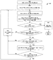
도 3은 2 개 이상의 에칭 스테이지 측정 목표를 충족하기 위하여 구성된 에칭 스테이지 프로세싱을 모니터하는 에칭 스테이지 측정 시스템을 이용하는 프로세스의 예시적인 흐름도를 나타낸다.
도 4는 2 개 이상의 에칭 스테이지 측정 목표를 충족하기 위하여 구성된 2 개의 이상의 광학적 메트롤로지 디바이스를 이용하여 에칭 프로세스를 모니터하는 예시적인 흐름도를 나타낸다.
도 5는 에칭 스테이지 측정 목표를 충족하기 위하여 구성된 2 개 이상의 광학적 메트롤로지 디바이스 및 적어도 하나의 에칭 센서 디바이스를 이용하여 에칭 프로세스를 모니터하는 예시적인 흐름도를 나타낸다.
도 6은 에칭 스테이지 측정 목표를 충족하기 위하여 구성된 복수의 광학적 메트롤로지 디바이스 및 에칭 센서 디바이스를 이용하여 에칭 프로세스를 모니터하는 예시적인 흐름도를 나타낸다.
도 7은 광학적 메트롤로지 디바이스 및 메트롤로지 프로세서를 구비하는 에칭 스테이지 측정 시스템을 나타내는 예시적인 건축상의 도면이다.
도 8은 광학적 메트롤로지 디바이스, 에칭 센서 디바이스, 신호 평가기 및 에칭 스테이지 추출기를 구비하는 에칭 스테이지 측정 시스템을 나타내는 예시적인 건축상의 도면이다.
도 9는 실시간 에칭 스테이지 측정 시스템의 예시적인 흐름도를 나타낸다.
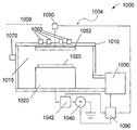
도 10은 2 개 이상의 광학적 메트롤로지 디바이스를 이용한 에칭 스테이지 측정 시스템을 가진 에칭 시스템을 나타내는 예시적인 건축상의 도면이다.
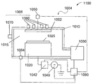
도 11은 2 개 이상의 광학적 메트롤로지 디바이스 및 적어도 하나의 에칭 센서 디바이스를 이용한 에칭 스테이지 측정 시스템을 가진 에칭 시스템을 나타내는 예시적인 건축상의 도면이다.
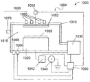
도 12는 2 개 이상의 광학적 메트롤로지 디바이스 및 복수의 에칭 센서 디바이스를 이용한 에칭 스테이지 측정 시스템을 가진 에칭 시스템을 나타내는 예시적인 건축상의 도면이다.
도 13a는 광학적 방사 분광에 대한 뷰포트를 가진 예시적인 에칭 시스템의 정면도를 나타내는 반면에 도 13b는 광학적 분광 및/또는 간섭 툴에 대한 에칭 시스템의 상부에 복수의 광학적 메트롤로지 디바이스에 대한 뷰포트를 가진 예시적인 에칭 시스템의 정면도를 나타낸다.1A is an architectural view illustrating a prior art method of using metrology data to control a process before or after a substrate fabrication flow.
1B is an architectural view of a prior art etching measurement system for utilizing optical metrology data.
Figure 2 shows an exemplary architectural drawing showing a real-time process control system that utilizes an etch stage measurement system to adjust at least one process parameter or tool setting in the same or different manufacturing clusters.
Figure 3 illustrates an exemplary flow diagram of a process utilizing an etch stage measurement system to monitor etch stage processing configured to meet two or more etch stage measurement objectives.
Figure 4 shows an exemplary flow chart for monitoring an etching process using two or more optical metrology devices configured to meet two or more etching stage measurement objectives.
5 illustrates an exemplary flow chart for monitoring an etch process using two or more optical metrology devices and at least one etch sensor device configured to meet an etch stage measurement objective.
Figure 6 illustrates an exemplary flow chart for monitoring an etch process using a plurality of optical metrology devices and etch sensor devices configured to meet etch stage measurement objectives.
Figure 7 is an exemplary architectural drawing showing an etching stage measurement system with an optical metrology device and a metrology processor.
8 is an exemplary architectural drawing showing an etching stage measurement system comprising an optical metrology device, an etching sensor device, a signal evaluator and an etching stage extractor.
Figure 9 shows an exemplary flow diagram of a real-time etch stage measurement system.
Figure 10 is an exemplary architectural drawing showing an etching system with an etching stage measurement system using two or more optical metrology devices.
11 is an exemplary architectural drawing showing an etching system with an etching stage measurement system using two or more optical metrology devices and at least one etching sensor device.
12 is an exemplary architectural drawing showing an etching system with an etching stage measurement system using two or more optical metrology devices and a plurality of etching sensor devices.
Figure 13a shows a front view of an exemplary etching system with a viewport for optical radiation spectroscopy, while Figure 13b shows a viewport with a viewport for a plurality of optical metrology devices on top of an etching system for optical spectroscopy and / or interference tools 1 shows a front view of an exemplary etching system.
본 발명의 설명을 용이하게 하기 위하여, 반도체 웨이퍼가 개념의 적용을 예시하기 위하여 이용될 수 있다. 방법 및 프로세스는 반복적인 구조를 가지는 다른 워크피스에 균등하게 적용된다. 이 워크피스는 웨이퍼, 기판, 디스크 등 일 수 있다. 또한, 이 애플리케이션에서, 구조라는 용어는 양자화되지 않는 경우에 패턴화된 구조를 나타낸다.In order to facilitate the description of the present invention, semiconductor wafers may be used to illustrate the application of the concept. The method and process are equally applied to other workpieces having an iterative structure. The workpiece may be a wafer, a substrate, a disk, or the like. Also, in this application, the term structure refers to a patterned structure when not quantized.
*도 1a는 워크피스 제조 흐름에 있어서 이전 또는 이후의 프로세스를 제어하기 위한 메트롤로지 데이터를 이용하는 종래 기술의 방법을 나타내는 건축상의 도면이다. 제조 스테이지 측정에 대한 종래 기술은 일반적으로 워크피스(미도시)에 제1 제조 프로세스(104)를 수행하는 제조 시스템(100)을 포함한다. 이 워크피스는 기판, 웨이퍼 또는 자기 메모리 등 일 수 있다. 제1 제조 프로세스(104)의 시작 또는 제1 제조 프로세스(104)의 종료로부터의 세트 시간 간격 이후에, 워크피스는 제1 메트롤로지 프로세스(108)를 이용하여 측정된다. 워크피스 애플리케이션에 대한 레시피에 기초하여, 제1 메트롤로지 프로세스(108)로부터의 측정 데이터(124)는 예상된 결과와 비교되고, 제조 클러스터 제어기(미도시) 또는 제1 제조 프로세스(104) 또는 제2 제조 프로세스(112) 중 어느 하나로 전송된다. 제1 메트롤로지 프로세스(108)로부터의 측정 데이터(124)가 예상된 결과의 범위 밖에 있는 경우, 제1 제조 프로세스(112) 또는 제1 제조 프로세스(104)에 신호가 전송될 수 있다. 이와 유사하게, 제2 제조 프로세스(112)의 시작으로부터 또는 제2 제조 프로세스(112)의 종료에서의 설정된 시간 간격 이후에, 워크피스는 제2 메트롤로지 프로세스(116)를 이용하여 측정되고, 제조 및 측정은 애플리케이션 레시피에 의해 결정됨에 따라 반복된다. 제1 제조 프로세스(104)에 전송된 측정 데이터(124)는 제1 제조 프로세스(104)에서의 프로세스 파라미터 또는 툴 세팅을 조정하는데 이용될 수 있다. 이와 유사하게, 제2 제조 프로세스(112)에 전송된 측정 데이터(124)는 제2 제조 프로세스(112)에서 프로세스 파라미터 또는 툴 세팅을 조정하는데 이용될 수 있다.1A is an architectural drawing showing a prior art method of using metrology data to control a process before or after a workpiece manufacturing flow. The prior art for manufacturing stage measurement generally includes a
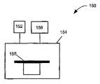
도 1b는 광학적 메트롤로지 데이터를 이용하는 종래 기술의 에칭 측정 시스템의 건축상의 도면이다. 예컨대, 에칭 측정 시스템(150)은 프로세싱 챔버(154) 및 웨이퍼 홀더 상의 웨이퍼를 구비한다. 프로세싱 챔버(154)는 측정을 수행하여 에칭 종점을 결정하기 위하여 프로세싱 챔버(154)에 연결된 제1 광학적 메트롤로지 디바이스(152) 및 제2 광학적 메트롤로지 디바이스(156)를 포함할 수 있다. 1B is an architectural view of a prior art etching measurement system using optical metrology data. For example, the
전술한 바와 같이, 종래 기술에 대한 결점은, 광학적 에칭 측정 시스템의 정확도 및 적합성이 반도체 애플리케이션 또는 애플리케이션의 범위에 대하여 작용하는 적절한 메트롤로지 툴을 선택하는데 있어서 문제점을 포함한다는 점이다. 또한, 기술은 파장 또는 파장들을 선택하기 위한 이전의 지식 및 이력 데이터, 특정한 광학적 메트로로지 디바이스 및 측정 모니터링 목표를 충족시키기 위한 에칭 스테이지 측정의 추출을 위한 알고리즘을 필요로 한다. 또한, 통합된 메트롤로지 제조 클러스터에 있어서, 목표화된 시간 범위를 충족시키기 위하여 실시간으로 에칭 측정 및 에칭 스테이지 데이터의 추출을 완료할 필요가 있다.As noted above, the drawback to the prior art is that the accuracy and suitability of the optical etch measurement system involves problems in selecting an appropriate metrology tool to act on a range of semiconductor applications or applications. The technique also requires prior knowledge and historical data for selecting wavelengths or wavelengths, specific optical metrology devices, and algorithms for extraction of etch stage measurements to meet the measurement monitoring goals. In addition, in an integrated metrology manufacturing cluster, it is necessary to complete etching measurement and extraction of etching stage data in real time in order to meet the targeted time range.
본 발명은 전술한 몇 가지 문제점의 영향을 감소시키는 것에 관한 것이다. 처리량에 대한 요구가 증가함에 따라, 구조의 사이즈를 감소시키고, 소유권에 대한 비용을 더 낮출 필요가 있으며, 2 개 이상의 에칭 스테이지 측정 목표를 충족하기 위하여 에칭 스테이지 측정 시스템의 설계를 최적화할 필요성이 더 커진다.The present invention is directed to reducing the effects of some of the problems described above. As the demand for throughput increases, there is a need to reduce the size of the structure, lower the cost for ownership, and optimize the design of the etching stage measurement system to meet two or more etching stage measurement objectives It grows.
에칭 스테이지 측정 목표는 정확도, 신뢰 간격, 측정 및 추출 시간(MEAT), 반복성, 정밀도, 재현성, 전체 측정 불확실성(TMU), 소유권의 전체 비용 등을 포함할 수 있다. 정확도는 주사 전자 현미경(SEM), 원자간력 현미경(AFM) 등을 이용하여 확립된 에칭 스테이지의 실제 값 또는 레퍼런스값과 비교하여 에칭 스테이지의 측정된 또는 계산된 값 사이의 일치의 정도이다. 신뢰 간격은 에칭 스테이지 측정이 상한과 하한 사이에 포함될 확률이다. 예컨대, 50% 완료된 에칭 스테이지 측정은 예를 들어 에칭 스테이지 평균 +/-5%의 신뢰 간격을 가질 수 있다. 측정 및 추출 완료의 속도는 밀리초 이하로 측정될 수 있다. 반복성 또는 검사 재검사 신뢰도는, 에칭 구조에 대하여 동일한 조건 하에서 하나의 사람 또는 기구에 의해 취해진 측정에서의 변화이며, 반복성 계수로서 표현될 수도 있고, 2 개 이상의 반복된 테스트 결과 사이의 절대적 차이가 예를 들어 95 퍼센트의 가능성을 가지도록 예상될 수 있는 값이다. 재현성은 통상적으로 표준 편차로서 표현되는, 다른 메트로롤지 시스템을 이용하여 동일한 결과를 획득하는 에칭 스테이지 측정 시스템의 능력이다. TMU는 선형 회귀 분석에 기초하며, 순잔여 에러로부터 레퍼런스 측정 시스템 불확실성(URMS)를 제거함으로써 산출된다. 메트롤로지 기구에 대한 TMU를 산출하는 것에 대한 상세한 설명에 대해서는, 2007년 10월 23일자로 발행되며, "ASSESSMENT AND OPTIMIZATION FOR METROLOGY INSTRUMENT INCLUDING UNCERTAINTY OF TOTAL MEASUREMENT UNCERTAINTY"으로 명명된 미국 특허 제7,286,247호를 참조하며, 이는 그 전체가 여기에 참고로 포함된다. 소유권에 대한 전체 비용은 때때로 내부 수익률 또는 경제적 부가 가치에 대하여 언급되는 취득 비용 및 작동 비용을 포함한다. 2 개 이상의 에칭 스테이지 측정 목표는 에칭 측정 시스템이 설계를 최적화하는데 이용될 수 있다.The etch stage measurement objectives may include accuracy, confidence interval, measurement and extraction time (MEAT), repeatability, precision, reproducibility, total measurement uncertainty (TMU), and total cost of ownership. Accuracy is the degree of agreement between the measured or calculated values of the etch stage compared to the actual or reference value of the etch stage established using a scanning electron microscope (SEM), an atomic force microscope (AFM), or the like. The confidence interval is the probability that the etch stage measurement will be included between the upper and lower limits. For example, a 50% completed etching stage measurement may have a confidence interval of, for example, an etching stage average +/- 5%. The rate of measurement and extraction completion can be measured in milliseconds or less. Repeatability or test retest reliability is a change in a measurement taken by one person or instrument under the same conditions for an etched structure and may be expressed as a repeatability coefficient and the absolute difference between two or more repeated test results It is a value that can be expected to have 95 percent probability. Reproducibility is the ability of an etching stage measurement system to obtain the same results using different metrology systems, typically expressed as standard deviations. The TMU is based on linear regression analysis and is calculated by removing the reference measurement system uncertainty (U RMS ) from the net residual error. For a detailed description of calculating the TMU for a metrology device, see U.S. Patent No. 7,286,247, issued October 23, 2007, entitled " ASSESSMENT AND OPTIMIZATION FOR METROLOGY INSTRUMENT INCLUDING UNCERTAINTY OF TOTAL MEASUREMENT UNCERTAINTY " , Which is hereby incorporated by reference in its entirety. The total cost of ownership includes the acquisition and operating costs, sometimes referred to as internal returns or economic added value. More than two etch stage measurement targets may be used to optimize the design of the etch measurement system.
도 2는 추출된 스테이지 측정값을 이용하여 제1 제조 클러스터(202) 또는 제2 제조 클러스터(206)에서 적어도 하나의 프로세스 파라미터 또는 툴 세팅을 조정하기 위하여 에칭 스테이지 측정 시스템(EMES)(204)를 이용하여 실시간 프로세스 제어를 수행하도록 구성되는 실시간 에칭 프로세스 제어 시스템(200)을 나타내는 예시적인 건축상의 도면을 나타낸다. 에칭 프로세스 제어 시스템(200)은, 제1 제조 클러스터(202)가 ESMS(204)에 연결되는 상태로 제1 제조 클러스터(202)에서 행해지고 있는 에칭 프로세스의 에칭 스테이지를 측정하도록 구성된다. 이 ESMS(204)는 메트롤로지 프로세서(216), 광학적 메트롤로지 디바이스(208) 및 에칭 센서 디바이스(212)를 구비한다. 광학적 메트롤로지 디바이스(208)는 광학적 방사 분광 디바이스 및/또는 하나 이상의 분광 반사계, 엘립소미터 및/또는 간섭계일 수 있다. 일 실시형태에서, 메트롤로지 프로세서(216)는 독립형 프로세서일 수 있다. 또 다른 실시형태에서, 메트롤로지 프로세서(216)는 제1 제조 클러스터(202)에 대하여 국부적으로 위치될 수 있거나, 또는 인터넷 또는 인트라넷을 통하여 제1 제조 클러스터(202)에 대하여 원격으로 위치될 수 있다. 이에 따라, 메트롤로지 프로세서(216)는, 직접 접속, 인트라넷 또는 인터넷 중 적어도 하나를 이용하여, 제1 제조 클러스터(202)와 데이터를 교환할 수 있다. 메트롤로지 프로세서(216)는 커스터머 사이트(즉, 디바이스 제조자 등)에서 인트라넷에 연결될 수 있거나 또는 벤더 사이트(즉, 장비 제조자)에서 인트라넷에 연결될 수 있다. 또한, 또 다른 컴퓨터(즉, 제어기, 서버 등)는 직접 접속, 인트라넷 또는 인터넷 중 적어도 하나를 통하여 데이터를 교환하기 위하여 메트롤로지 프로세서(216)에 액세스할 수 있다.FIG. 2 illustrates an etching stage measurement system (EMES) 204 for adjusting at least one process parameter or tool setting in a first fabrication cluster 202 or a second fabrication cluster 206 using extracted stage measurements. Time
에칭 센서 디바이스(212)는 에칭 스테이지, 에칭 레이트, 에칭 선택도 및/또는 기판 전체에 걸친 에칭 균일성과 상관되는 에칭 프로세스 파라미터를 측정하는 디바이스일 수 있다. 예컨대, 에칭 센서 디바이스(212)는 프로세싱 챔버에 인가된 전력, 전압, 위상, 전류와, 사용된 가스의 압력, 에천트 가스 흐름, 가스 비율과, 전달된 무선 주파수와, 온도 등의 프로세스 파라미터를 측정하는 디바이스를 포함할 수 있다. 에칭 센서 디바이스(212)는 하나 이상의 전술한 프로세스 파라미터를 측정할 수 있는 하나 이상의 상이한 타입의 디바이스일 수 있다. ESMS(204) 내의 메트롤로지 프로세서(216)는 제1 제조 클러스터(202) 및 제 2 제조 클러스터(206)에 국부적으로 연결된 프로세서일 수 있다. 대안적으로, 메트롤로지 프로세서(216)는 인트라넷, 여러 가지 프로세서의 전용 네트워크를 통하여 원격으로 제1 제조 클러스터(202) 및 제2 제조 클러스터(206)에 연결될 수 있거나, 또는 인터넷을 통하여 접속된다. 메트롤로지 프로세서(216)는, 광학적 메트롤로지 디바이스 및/또는 에칭 센서 디바이스로부터 에칭 스테이지 값 또는 실시간에서의 에칭 완료 퍼센트로의 측정의 변환, 강화 및 전환을 용이하게 하기 위한 명령 코드 또는 소프트웨어 코드와, 입력 디바이스, 디스플레이, 스토리지, 제어기를 포함할 수 있다. 이하에서는, ESMS(204)에서 이용된 단계들의 세부사항을 명세서의 균형을 맞추어 설명한다.The
도 2를 다시 참조하면, 제1 제조 클러스터(202)는 ESMS(204) 및 제2 제조 클러스터(206)에 연결된 에칭 프로세스 툴(미도시)을 포함한다. 일 실시형태에서, 제2 제조 클러스터(206)는, 클리닝 프로세스 툴, 증착 프로세스 툴, 포토리소그래피 툴 또는 또 다른 에칭 툴을 포함할 수 있고, 제조 흐름에 있어서 제1 제조 클러스터(202) 이후에 배치될 수 있다. 또 다른 실시형태에서, 제2 제조 클러스터(206)는 클리닝 프로세스 툴, 증착 프로세스 툴, 포토리소그래피 툴 또는 또 다른 에칭 툴을 포함할 수 있고, 제조 흐름에 있어서 제1 제조 클러스터(202) 이전에 배치될 수 있다.Referring again to FIG. 2, the first manufacturing cluster 202 includes an etch process tool (not shown) coupled to the
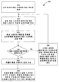
도 3은 2 개 이상의 에칭 스테이지 측정 목표를 충족시키도록 구성되는 에칭 프로세싱을 모니터하기 위하여 에칭 스테이지 측정 시스템(ESMS)을 이용한 기판 프로세스의 예시적인 흐름도(300)를 나타낸다. 단계 304에서, 2 개 이상의 에칭 스테이지 측정 목표가 설정된다. 전술한 바와 같이, 2 개 이상의 에칭 스테이지 측정 목표는, 정확도, 신뢰 간격, 측정 및 추출 시간(MAET), 반복성, 재현성, 전체 측정 불확실성(TMU) 및/또는 소유권의 전체 비용을 포함할 수 있다. 일 실시형태에서, 2 개 이상의 에칭 스테이지 측정 목표는 정확도와 측정 및 추출 시간을 포함한다. 또 다른 실시형태에서, 정확도는 0.95 이상으로 설정될 수 있고, 측정 및 추출 시간은 6.0 밀리초 이하로 설정될 수 있다. MAET는 반도체 애플리케이션 레시피 및 기판 처리량의 필요조건을 충족하는 시간의 범위일 수 있다. 또 다른 실시형태에서, 2 개 이상의 에칭 스테이지 측정 목표는, 정확도와 측정 및 추출 시간과 5% 이하의 TMU를 포함한다. 또 다른 실시형태에서, 2 개 이상의 에칭 스테이지 측정 목표는, 정확도와 측정 및 추출 시간과, 2 개 이상의 반복된 테스트 결과가 95% 이상의 확률로 동일하게 되는 반복성 계수로서 표현되는 반복성을 포함한다.Figure 3 shows an
단계 308에서, 실제 에칭 스테이지 데이터에 대한 에칭 스테이지 측정의 상관관계를 전개한다. 실제 에칭 스테이지 데이터는 에칭 프로세스의 완료의 레퍼런스값일 수 있으며, 예컨대, 에칭 스테이지 데이터는, 에칭될 타겟층 또는 층들이 90% 완료인 경우에, 90%일 수 있다. 대안적으로, 실제 에칭 스테이지 데이터는, 에칭된 층 또는 층들의 실제 높이 예컨대 50 나노미터의 질화 실리콘층으로 표현될 수 있다. 실제 에칭 스테이지 데이터는 도쿄 엘렉트론 가부시키가이샤 및 KLA-Tencor 주식회사에 의해 소유된 AcuShapeTM와 같은, SEM, AFM 또는 광학적 디지털 프로필로메트리를 이용하는 등의 레퍼런스 측정 시스템을 이용하여 획득될 수 있다. 전술한 바와 같이, 에칭 스테이지 데이터는 기판에서의 하나 이상의 층의 에칭 프로세스의 완료율로서 표현될 수 있다. 일 실시형태에서, 실제 에칭 스테이지 데이터에 대한 에칭 스테이지 측정의 상관관계는 1차 방정식의 형태일 수 있다. 또 다른 실시형태에서, 상관관계는 예를 들어 상이한 광학적 메트롤로지 디바이스를 이용하여 측정된 에칭 스테이지 측정 및 상이한 에칭 센서 디바이스를 이용하여 측정된 센서 측정의 임의의 수에 들어 맞을 수 있는 2차 다항식으로서 더욱 일반적으로 표현될 수 있다.At
변수의 선형 관계가 전술한 예에서 사용되었지만, 임의의 함수, 합성 함수 등의 변수 사이의 비선형 함수 관계를 이용할 수 있다는 것을 인식해야 한다. 다항식에 대한 최소 제곱법 솔루션은, 행렬식, 매트릭스, 독립 파라미터 솔루션 등을 포함할 수 있다. 임의의 함수에 대한 최소 제곱법은, 비선형 피팅 방법, 검색 파라미터 이격 방법, 경사도 검색 방법, 확대 방법, 마쿼트 방법 등을 포함할 수 있다. 이들 기술의 더욱 상세한 설명에 대해서는, Bevington 등에 의한 "Data Reduction and Error Analysis for the Physical Sciences", 제3판, 116-117 페이지를 참조하며, 이는 여기에 참고로 통합된다.It should be appreciated that although the linear relationship of the variables is used in the above example, it is possible to use a non-linear function relationship between variables such as arbitrary functions, synthesis functions, and the like. The least squares solution for a polynomial may include determinant, matrix, independent parameter solution, and so on. The least squares method for an arbitrary function may include a nonlinear fitting method, a search parameter spacing method, a gradient search method, an enlargement method, a magic method, and the like. For a more detailed description of these techniques, see Bevington et al., &Quot; Data Reduction and Error Analysis for the Physical Sciences ", 3rd ed., Pages 116-117, incorporated herein by reference.
도 3을 다시 참조하면, 단계 308에서, 전개된 상관관계는, 에칭 스테이지 측정 및 대응하는 실제 에칭 스테이지 데이터를 구비하는 데이터베이스 또는 라이브러리와 같은 데이터 스토어일 수 있다. 예컨대, 데이터베이스 또는 라이브러리는, 함수 또는 파장으로서의 빔 세기 및 대응하는 실제 에칭 스테이지 데이터와 같은 광학적 메트롤로지 측정을 포함할 수 있다. 또 다른 실시형태에서, 전개된 상관관계는 출력 에칭 스테이지 데이터를 결정하기 위하여 광학적 메트롤로지 측정을 입력하도록 트레이닝된 머신 학습 시스템일 수 있다.Referring back to FIG. 3, at
단계 312에서, 에칭 스테이지 값은 에칭 스테이지 측정 및 전개된 상관관계를 이용하여 추출된다. 실시형태에서, 에칭 스테이지 측정은 2 개 이상의 광학적 메트롤로지 측정일 수 있다. 또 다른 실시형태에서, 에칭 스테이지 측정은 2 개 이상의 광학적 메트롤로지 측정 및 적어도 하나의 에칭 센서 측정일 수 있다. 또 다른 실시형태에서, 에칭 스테이지 측정은 복수의 광학적 메트롤로지 측정 및 복수의 에칭 센서 측정일 수 있다. 단계 316에서, 결정된 에칭 스테이지 값은 에칭 스테이지 측정 목표가 충족되는지를 계산하는데 이용된다. 실시형태에서, 에칭 스테이지 측정 목표는, 0.95 이상의 에칭 스테이지 정확도 및 2.0 밀리초 이하의 측정 및 추출 시간을 포함한다. 에칭 스테이지 값을 이용하여 산출된 에칭 스테이지 정확도는 0.95와 비교되고, 측정 및 추출 시간의 실제로 경과된 전체 시간은 2 밀리초와 비교된다. 또 다른 실시형태에서, 에칭 스테이지 측정 목표는, 0.95 이상의 에칭 스테이지 정확도 및 2.0 밀리초 이하의 측정 및 추출 시간 이외에, 신뢰 간격 예컨대, 에칭 스테이지 평균 +/- 5%를 포함할 수 있다.In
에칭 스테이지 측정 목표가 충족되지 않으면, 단계 324에서, 상기 메트롤로지 디바이스는 변경되고, 에칭 스테이지 측정은 향상되고, 및/또는 상관관계 알고리즘은 개선된다. 광학적 메트롤로지 디바이스의 변경은, 광학적 메트롤로지 디바이스에서의 광학적 구성요소를 조정하거나 또는 광학적 구성요소의 일부를 변경함으로써 행해질 수 있다. 광학적 메트롤로지 디바이스의 설계 변경에 대한 더욱 상세한 설명에 대해서는, 2010년 7월 10일자로 발행되고, "AN OPTICAL METROLOGY SYSTEM OPTIMIZED WITH DESIGN GOALS"로 명명되며, 그 전체가 여기에 참고로 포함된 미국 특허 제7,761,250호를 참조한다. 또 다른 실시형태에서, 선택된 메트롤로지 센서 디바이스를 예컨대, 온도 센서 대신에 압력 센서를 선택함으로써 변경할 수 있다. 에칭 스테이지 측정은 신호에서의 노이즈를 조정함으로써 향상될 수 있다. 시스템적인 노이즈는 측정될 애플리케이션의 범위에 대하여 기판 샘플이 갖는 광학적 메트롤로지 디바이스의 캘리브레이션을 통하여 조정될 수 있다. 광학적 메트롤로지 신호 노이즈 감소에 대한 상세한 설명에 대해서는, 2010년 6월 22일자로 발행되며, 그 전체가 여기에 참고로 포함되며,“NOISE-REDUCTION METROLOGY MODELS"로 명명된 미국 특허 제7,742,177호를 참조한다. 상관관계 알고리즘을 개선하는 것은 선형 상관계를 이용하는 것으로부터 비선형 상관관계를 이용하는 것으로 기술을 변경하는 것을 포함할 수 있으며 즉, 변수 사이의 비선형 함수 관계를 이용할 수 있다. 전술한 바와 같이, 비선형 함수 관계는 임의의 함수, 합성 함수 등을 포함한다. 다항식에 대한 최소 제곱법 솔루션은, 행렬식, 매트릭스, 독립 파라미터 솔루션 등을 포함할 수 있다. 임의의 함수에 대한 최소 제곱법은 비선형 피팅 방법, 검색 파라미터 이격 방법, 격자 탐색 방법, 기울기 검색 방법, 확대 방법, 마쿼트 방법 등을 포함할 수 있다.If the etch stage measurement target is not met, then at
도 3을 다시 참조하면, 단계 320에서, 추출된 에칭 스테이지 값을 전송한다. 일 실시형태에서, 에칭 스테이지 값은, 제1 제조 클러스터(202) 또는 제2 제조 클러스터(206)에 연결될 수 있는 메트롤로지 프로세서(도 2, 216)에 전송된다. 도 3의 단계 328에서, 전송된 에칭 스테이지 값은, 제1 제조 클러스터(202) 또는 제2 제조 클러스터(206)의 적어도 하나의 에칭 프로세스 제어 파라미터 또는 장비 세팅을 변경하는데 이용된다.Referring again to FIG. 3, in
도 4, 5, 및 6은 에칭 스테이지 측정 디바이스의 상이한 조합을 이용하여 실제 에칭 스테이지 데이터에 대한 에칭 스테이지 측정의 상관관계를 전개하기 위한 예시적인 흐름도를 나타낸다. 도 4는 2 개 이상의 광학적 메트롤로지 디바이스를 이용하는 흐름도를 나타내는 반면에 도 5는 2 개 이상의 광학적 메트롤로지 디바이스 및 적어도 하나의 에칭 센서 디바이스를 이용하는 흐름도를 나타낸다. 도 6은 2 개 이상의 광학적 메트롤로지 디바이스 및 2 개 이상의 에칭 센서 디바이스를 이용할 수 있는 경우에서의 복수의 메트롤로지 기술을 이용하는 흐름도를 나타낸다.Figures 4, 5, and 6 illustrate an exemplary flow chart for developing a correlation of etch stage measurements to actual etch stage data using different combinations of etch stage measurement devices. Figure 4 shows a flow diagram using two or more optical metrology devices, while Figure 5 shows a flow diagram using two or more optical metrology devices and at least one etch sensor device. Figure 6 shows a flow diagram using a plurality of metrology techniques in the case where two or more optical metrology devices and two or more etch sensor devices are available.
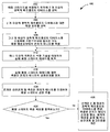
도 4는 에칭 스테이지 측정 목표를 충족하도록 구성되는 2 개 이상의 광학적 메트롤로지 디바이스를 이용하여 실제 에칭 스테이지 데이터에 대한 에칭 스테이지 측정의 상관관계를 전개하기 위한 예시적인 흐름도(400)를 나타낸다. 단계 402에서, 에칭 스테이지를 측정하기 위하여 2 개 이상의 광학적 메트롤로지 디바이스를 선택한다. 레시피에 의존하여, 에칭 스테이지는 기판의 하나 이상의 층의 부분적인 또는 전체적인 에칭일 수 있다. 선택된 2 개 이상의 광학적 메트롤로지 디바이스는, 광학적 방사 분광 디바이스, 간섭계, 반사계, 엘립소미터의 조합 또는 전술한 것의 임의의 조합일 수 있다. 단계 404에서, 파장 또는 파장의 범위는 2 개 이상의 광학적 메트롤로지 디바이스에 대하여 선택될 수 있다. 일 실시형태에서, 파장 범위는 120 내지 190 nm일 수 있다. 다른 실시형태에서, 파장 범위는 170 내지 190 nm일 수 있다. 또 다른 실시형태에서, 파장 범위는 120 내지 1000 nm일 수 있다. 파장 범위의 선택은, 기판 애플리케이션, 유사한 애플리케이션에 대한 이전의 역사적 경험, 광학적 메트롤로지 디바이스의 벤더 및 설정된 2 개 이상의 에칭 스테이지 측정 목표에 기초한다.4 shows an
단계 408에서, 워크피스로부터 떨어져 회절되거나 또는 에칭 챔버로부터의 전자기 에너지를, 그 선택된 2 개 이상의 광학적 메트롤로지 디바이스를 이용하여 측정한다. 단계 412에서, 측정된 전자기 에너지에 대응하는 실제 에칭 스테이지 데이터를 하나 이상의 레퍼런스 측정 기술을 이용하여 획득한다. 레퍼런스 측정 기술은 도쿄 엘렉트론 가부시키가이샤 및 KLA-Tencor 주식회사에 의해 소유된 AcuShapeTM와 같은, SEM, AFM 또는 광학적 디지털 프로필로메트리를 이용하는 것 등을 포함한다. 전술한 바와 같이, 실제 에칭 스테이지 데이터는, 에칭 프로세스의 완료의 레퍼런스값일 수 있으며, 실제 에칭 스테이지 데이터는, 에칭될 타겟층 또는 층들이 90% 완료된 경우에, 90%일 수 있다. 대안적으로, 실제 에칭 스테이지 데이터는, 에칭된 층 또는 층들의 실제 높이 예컨대 50 나노미터의 질화 실리콘층으로 표현될 수 있다.At
단계 416에서, 측정된 전자기 에너지 데이터는 실제 에칭 스테이지 데이터와 상관된다. 일 실시형태에서, 실제 에칭 스테이지 데이터에 대한 에칭 스테이지 측정의 상관관계는 1차 방식의 형태일 수 있다. 대안적으로, 상관관계는 임의 함수, 합성 함수 등과 같은 변수의 선형 관계 또는 그 변수 사이의 비선형 함수 관계로서 표현될 수 있다. 다항식에 대한 최소 제곱법 솔루션은, 행렬식, 매트릭스, 독립 파라미터 솔루션 등을 포함할 수 있다. 임의의 함수에 대한 최소 제곱법은, 비선형 피팅 방법, 탐색 파라미터 이격 방법, 격자 탐색 방법, 기울기 탐색 방법, 확대 방법, 마쿼트 방법 등을 포함할 수 있다. 전술한 바와 같이, 이러한 기술에 대한 더욱 상세한 설명에 대해서는, Bevington 등에 의한 "Data Reduction and Error Analysis for the Physical Sciences,", 제3판, 페이지 116-117을 참조하며, 이는 여기에 참고로 통합된다.In
단계 416을 다시 참조하면, 일 실시형태에서, 전개된 상관관계는 에칭 스테이지 측정 및 대응하는 실제 에칭 스테이지 데이터를 구비하는 데이터베이스 또는 라이브러리와 같은 데이터 스토어일 수 있다. 예컨대, 데이터베이스 또는 라이브러리는, 함수 또는 파장으로서의 빔 세기 및 대응하는 에칭 완료 데이터와 같은 광학적 메트롤로지 측정을 포함할 수 있다. 또 다른 실시형태에서, 전개된 상관관계는 출력 에칭 스테이지 데이터를 결정하기 위하여 광학적 메트롤로지 측정을 입력하도록 트레이닝된 머신 학습 시스템일 수 있다.Referring back to step 416, in one embodiment, the evolved correlation may be a data store, such as a database or library, with an etch stage measurement and corresponding actual etch stage data. For example, the database or library may include optical metrology measurements, such as beam intensity as a function or wavelength, and corresponding etch completion data. In another embodiment, the evolved correlation may be a machine learning system trained to input optical metrology measurements to determine output etch stage data.
단계 420에서, 에칭 스테이지 측정 및 전개된 상관관계를 이용하여 에칭 스테이지 값을 추출한다. 일 실시형태에서, 에칭 스테이지 측정은 2 개 이상의 광학적 메트롤로지 측정일 수 있다. 단계 424에서는, 도 3의 단계 304에서 설정된 에칭 스테이지 측정 목표가 충족되는지 여부를 계산하는데, 결정된 에칭 스테이지 값을 이용한다. 일 실시형태에서는, 에칭 스테이지 측정 목표가 0.95 이상의 정확도와 2.0 밀리초 이하의 측정 및 추출 시간을 포함한다고 가정한다. 산출된 정확도는 0.95와 비교되고, 측정 및 추출 시간의 실제로 경과된 시간은 2 밀리초와 비교된다. 또 다른 실시형태에서, 에칭 측정 목표는, 0.95 이상의 에칭 스테이지 정확도 및 2.0 밀리초 이하의 측정 및 추출 시간 이외에, 신뢰 간격 예컨대, 에칭 스테이지 평균 +/- 5%를 포함할 수 있다.In
에칭 스테이지 측정 목표가 충족되지 않으면, 단계 428에서, 2 개 이상의 메트롤로지 디바이스는 변경되고, 에칭 스테이지 측정은 향상되고, 메트롤로지 조명 빔에 사용되는 최적의 파장이 결정되고, 및/또는 상관 알고리즘이 개선된다. 광학적 메트롤로지 디바이스의 변경은, 광학적 메트롤로지 디바이스에서의 광학적 구성요소를 조정하거나 또는 광학적 구성요소의 일부를 변경함으로써 행해질 수 있다. 또 다른 실시형태에서, 에칭 애플리케이션의 타입에 따라서, 에칭 챔버는 회절 신호를 강화시키기 위하여 질소 또는 희가스로 퍼지될 수 있다. 대안적으로, 측정된 에칭 스테이지 신호의 향상은 신호의 노이즈를 조정함으로써 행해질 수 있다. 시스템적인 노이즈는 측정될 애플리케이션의 범위에 대하여 기판 샘플을 갖는 광학적 메트롤로지 디바이스의 캘리브레이션을 통하여 조정될 수 있다.If the etch stage measurement target is not met, then in
최적의 파장은, 회귀 기술 또는 그와 유사한 기술을 이용하여 광학적 메트롤로지 디바이스에 대하여 결정된다. 광학적 메트롤로지에 대한 파장 선택을 최적화는 것에 대한 상세한 설명에 대해서는, 2007년 5월 8일자로 발행되고, "SELECTION OF WAVELENGTHS FOR INTEGRATED CIRCUIT OPTICAL METROLOGY"로 명명되며, 그 전체가 여기에 참고로 포함된 미국 특허 제7,216,045호를 참조한다. 상관관계 알고리즘을 개선하는 것은 선형 상관관계를 이용하는 것으로부터 비선형 상관관계를 이용하는 것으로 기술을 변경하는 것을 포함할 수 있으며 즉, 변수 사이의 비선형 함수 관계를 이용할 수 있다. 전술한 바와 같이, 비선형 함수 관계는 임의의 함수, 합성 함수 등을 포함한다. 다항식에 대한 최소 제곱법 솔루션은, 행렬식, 매트릭스, 독립 파라미터 솔루션 등을 포함할 수 있다. 임의의 함수에 대한 최소 제곱법은 비선형 피팅 방법, 검색 파라미터 이격 방법, 격자 탐색 방법, 기울기 검색 방법, 확대 방법, 마쿼트 방법 등을 포함할 수 있다. 단계 428 이후에, 에칭 스테이지 측정 목표가 충족될 때 까지, 프로세스 단계 412 내지 432를 반복한다.The optimal wavelength is determined for the optical metrology device using a regression technique or the like. For a detailed description of optimizing wavelength selection for optical metrology, refer to " SELECTION OF WAVELENGTHS FOR INTEGRATED CIRCUIT OPTICAL METROLOGY "issued May 8, 2007, incorporated herein by reference in its entirety See U.S. Patent No. 7,216,045. Improving the correlation algorithm may involve changing the technique from using a linear correlation to using a non-linear correlation, i.e., using a nonlinear function relationship between the variables. As described above, the nonlinear function relation includes any function, a composite function, and the like. The least squares solution for a polynomial may include determinant, matrix, independent parameter solution, and so on. The least squares method for an arbitrary function may include a nonlinear fitting method, a search parameter spacing method, a grid search method, a slope search method, an enlargement method, a magic method, and the like. After
도 5는 에칭 스테이지 측정 목표를 충족하도록 구성된 2 개 이상의 광학적 메트롤로지 디바이스 및 적어도 하나의 에칭 센서 디바이스를 이용하여 실제 에칭 스테이지 데이터에 대한 에칭 스테이지 측정의 상관관계를 전개하기 위한 예시적인 흐름도(500)를 나타낸다. 단계 502에서, 에칭 스테이지를 측정하기 위하여 2 개 이상의 광학적 메트롤로지 디바이스를 선택한다. 레시피에 따라서, 에칭 스테이지는 워크피스의 하나 이상의 층의 부분적인 또는 전체적인 에칭일 수 있다. 선택된 2 개 이상의 광학적 메트롤로지 디바이스는 광학적 방사 분광 디바이스, 간섭계, 반사계, 엘립소미터의 조합 또는 전술한 것의 임의의 조합일 수 있다. 단계 504에서, 파장 또는 파장의 범위는 2 개 이상의 광학적 메트롤로지 디바이스에 대하여 선택될 수 있다. 일 실시형태에서, 파장 범위는 120 내지 190 nm일 수 있다. 다른 실시형태에서, 파장 범위는 170 내지 190 nm일 수 있다. 또 다른 실시형태에서, 파장 범위는 120 내지 1000 nm일 수 있다. 파장 범위의 선택은, 기판 애플리케이션, 유사한 애플리케이션에 대한 이전의 역사적 경험, 광학적 메트롤로지 디바이스의 벤더 및 설정된 2 개 이상의 에칭 스테이지 측정 목표에 기초한다.5 is an
단계 508에서, 에칭 스테이지와 실질적으로 상관된 측정에 따라 적어도 하나의 에칭 프로세스 센서 디바이스를 선택한다. 일 실시형태에서, 에칭 스테이지와 가장 높은 상관관계를 가지는 에칭 프로세스 센서가 선택된다. 적어도 하나의 프로세스 센서 디바이스의 선택은, 이들의 상호 관계를 식별하는데 도움을 줄 수 있는 프로세스 데이터의 세트, 메트롤로지 데이터(회절 신호) 및 프로세스 퍼포먼스 데이터를 이용하는 다변량 분석을 이용하여 행해질 수 있다. 예컨대, 다변량 분석은 선형 분석 또는 비선형 분석을 포함할 수 있다. 추가적으로, 예컨대, 다변량 분석은 주요 구성요소 분석(PCA), 독립 구성요소 분석, 교차 상관관계 분석, 선형 근사 분석 등을 포함할 수 있다. 주요한 변수를 식별하는데 다변량 분석을 이용하는 것에 대한 상세한 설명에 대해서는, 2008년 12월 16일자로 발행되며, "TRANSFORMING METROLOGY DATA FROM A SEMICONDUCTOR TREATMENT SYSTEM USING MULTIVARIATE ANALYSIS"으로 명명되며, 그 전체가 여기서 참고로 포함되는 미국 특허 제7,467,064호를 참조한다. 단계 512에서, 워크피스로부터 떨어져 회절된 또는 에칭 챔버로부터의 전자기 에너지를, 그 선택된 2 개 이상의 광학적 메트롤로지 디바이스를 이용하여 측정하며, 적어도 하나의 에칭 프로세스 센서 디바이스로부터의 측정이 획득된다.At
단계 516에서, 측정된 전자기 에너지에 대응하는 실제 에칭 스테이지 데이터 및 에칭 센서 측정을 하나 이상의 레퍼런스 측정 기술을 이용하여 획득한다. 레퍼런스 측정 기술은 도쿄 엘렉트론 가부시키가이샤 및 KLA-Tencor 주식회사에 의해 소유된 AcuShapeTM와 같은, SEM, AFM 또는 광학적 디지털 프로필로메트리를 이용하는 것 등을 포함한다. 전술한 바와 같이, 실제 에칭 스테이지 데이터는, 에칭 프로세스의 완료의 레퍼런스값일 수 있으며, 에칭 스테이지 데이터는, 에칭될 타겟층 또는 층들이 90% 완료인 경우에, 90%일 수 있다. 대안적으로, 실제 에칭 스테이지 데이터는, 에칭된 층 또는 층들의 실제 높이 예컨대 50 나노미터의 질화 실리콘층으로 표현될 수 있다.In
단계 520에서, 측정된 전자기 에너지 데이터 및 에칭 센서 측정은 실제 에칭 스테이지 데이터와 상관된다. 일 실시형태에 있어서, 실제 에칭 스테이지 데이터에 대한 에칭 스테이지 측정의 상관관계는 1차 방정식의 형태일 수 있다. 대안적으로, 상관관계는 변수의 선형 관계, 또는 임의의 함수, 합성 합수 등과 같은 변수 사이의 비선형 함수 관계로서 표현될 수 있다. 다항식에 대한 최소 제곱법 솔루션은, 행렬식, 매트릭스, 독립 파라미터 솔루션 등을 포함할 수 있다. 임의의 함수에 대한 최소 제곱법은 비선형 피팅 방법, 검색 파라미터 이격 방법, 격자 탐색 방법, 기울기 검색 방법, 확대 방법, 마쿼트 방법 등을 포함할 수 있다. 전술한 바와 같이, 이들 기술에 대한 더욱 상세한 설명에 대해서는, Bevington 등 의한, "Data Reduction and Error Analysis for the Physical Sciences", 제3판, 페이지 116-177을 참조하며, 이는 여기에 참고로 통합된다. In
단계 520를 다시 참조하면, 실시형태에 있어서, 전개된 상관관계는 에칭 스테이지 측정 및 대응하는 에칭 스테이지 데이터로서 구비하는 데이터베이스 또는 라이브러리와 같은 데이터 스토어일 수 있다. 예컨대, 데이터베이스 또는 라이브러리는, 파장의 함수로서의 빔 세기와 같은 광학적 메트롤로지 측정, 에칭 센서 측정 및 대응하는 에칭 스테이지 데이터를 포함할 수 있다. 또 다른 실시형태에서, 전개된 상관관계는 출력 에칭 스테이지 데이터를 결정하기 위하여 광학적 메트롤로지 측정 및/또는 에칭 센서 측정을 입력하도록 트레이닝된 머신 학습 시스템일 수 있다.Referring back to step 520, in an embodiment, the evolved correlation may be a data store such as a database or library provided as an etch stage measurement and corresponding etch stage data. For example, the database or library may include optical metrology measurements, such as beam intensity as a function of wavelength, etch sensor measurements and corresponding etch stage data. In another embodiment, the evolved correlation may be a machine learning system trained to input optical metrology measurements and / or etch sensor measurements to determine output etch stage data.
단계 524에서, 에칭 스테이지 측정 및 전개된 상관관계를 이용하여 에칭 스테이지값이 추출된다. 실시형태에서, 에칭 스테이지 측정은 2 개 이상의 광학적 메트롤로지 측정 및 적어도 하나의 에칭 센서 측정일 수 있다. 다른 실시형태에서, 에칭 스테이지 측정은 복수의 광학적 메트롤로지 측정 및 복수의 에칭 센서 측정일 수 있다. 단계 528에서, 결정된 에칭 스테이지 값은, 도 3의 단계 304에서 설정된 에칭 스테이지 측정 목표가 충족되는지 여부를 계산하는데 이용된다. 실시형태에서, 에칭 측정 목표는, 0.95 이상의 정확도 및 2.0 밀리초 이하의 측정 및 추출 시간을 포함한다. 산출된 에칭 스테이지 정확도는 0.95와 비교되고, 측정 및 추출 시간의 실제로 경과된 시간은 2 밀리초와 비교된다. 또 다른 실시형태에서, 에칭 스테이지 측정 목표는, 0.95 이상의 에칭 스테이지 정확도 및 2.0 밀리초 이하의 측정 및 추출 시간 이외에, 신뢰 간격 예컨대, 에칭 스테이지 평균 +/- 5%를 포함할 수 있다. 또 다른 실시형태에서, 에칭 스테이지 측정 목표는, 0.95 이상의 에칭 스테이지 정확도, 6.0 밀리초 이하의 측정 및 추출 시간, 및/또는 98%의 반복성을 포함한다.At
에칭 스테이지 측정 목표가 충족되지 않으면, 단계 532에서, 2 개 이상의 광학적 메트롤로지 디바이스가 변경될 수 있고, 에칭 스테이지 측정이 향상되고, 광학적 메트롤로지 디바이스에 의해 사용된 최적의 파장이 결정될 수 있고, 및/또는 상관관계 알고리즘이 개선될 수 있다. 광학적 메트롤로지 디바이스의 변경은, 광학적 메트롤로지 디바이스에서의 광학적 구성요소를 조정하거나 또는 광학적 구성요소의 일부를 변경함으로써 행해질 수 있다. 또 다른 실시형태에서, 선택된 에칭 센서는, 예컨대 온도 센서 대신에 압력 센서를 선택하여 변경될 수 있다. 또 다른 실시형태에서, 에칭 애플리케이션의 타입에 따라서, 에칭 챔버는 회절 신호를 강화시키기 위하여 질소 또는 희가스로 퍼지될 수 있다. 대안적으로, 측정된 에칭 스테이지 측정의 향상은 측정에서의 노이즈를 조정함으로써 행해질 수 있다. 시스템적인 노이즈는 측정될 애플리케이션의 범위에 대하여 기판 샘플을 갖는 광학적 메트롤로지 디바이스 및 적어도 하나의 에칭 센서 디바이스의 캘리브레이션을 통하여 조정될 수 있다.If the etch stage measurement target is not met, then in
최적의 파장은, 회귀 기술 또는 그와 유사한 기술을 이용하여 광학적 메트롤로지 디바이스에 대하여 결정될 수 있다. 상관관계 알고리즘을 개선하는 것은 선형 상관관계를 이용하는 것으로부터 변수 사이의 비선형 함수 관계와 같은 비선형 상관관계를 이용하는 것으로 기술을 변경하는 것을 포함할 수 있다. 전술한 바와 같이, 비선형 함수 관계는 임의의 함수, 합성 함수 등을 포함한다. 다항식에 대한 최소 제곱법 솔루션은, 행렬식, 매트릭스, 독립 파라미터 솔루션 등을 포함할 수 있다. 임의의 함수에 대한 최소 제곱법은 비선형 피팅 방법, 검색 파라미터 이격 방법, 격자 탐색 방법, 기울기 검색 방법, 확대 방법, 마쿼트 방법 등을 포함할 수 있다. 단계 532 이후에, 에칭 스테이지 측정 목표가 충족될 때 까지, 프로세스 단계 512 내지 532를 반복한다.The optimal wavelength can be determined for the optical metrology device using a regression technique or similar technique. Improving the correlation algorithm may involve changing the technique from using a linear correlation to using a nonlinear correlation, such as a nonlinear function relationship between variables. As described above, the nonlinear function relation includes any function, a composite function, and the like. The least squares solution for a polynomial may include determinant, matrix, independent parameter solution, and so on. The least squares method for an arbitrary function may include a nonlinear fitting method, a search parameter spacing method, a grid search method, a slope search method, an enlargement method, a magic method, and the like. After
도 6은 에칭 스테이지 측정 목표를 충족하도록 구성되는 복수의 메트롤로지 디바이스를 이용하여 실제 에칭 스테이지 데이터에 대한 에칭 스테이지의 상관관계를 전개하기 위한 예시적인 흐름도(600)를 나타낸다. 단계 604에서, 통합된 실시간 메트롤로지에 대한 에칭 스테이지를 측정하도록 복수의 메트롤로지 기술을 선택한다. 메트롤로지 기술은, 예컨대 광학적 방사 스펙트럼, 반사계, 엘립소미터 및/또는 간섭계와 같은 광학적 메트롤로지와, 예컨대, 워크피스의 하나 이상의 층의 에칭 완료와 같은 에칭 스테이지 데이터와 실질적으로 상관되는 측정을 가진 프로세스 센서와 같은 비광학적 메트롤로지를 포함한다. 단계 608에서, 선택된 복수의 메트롤로지 기술을 이용하여, 2 개 이상의 메트롤로지 디바이스는 에칭 스테이지를 측정하기 위하여 선택된다.Figure 6 shows an
하나 이상의 프로세스 센서 디바이스의 선택은, 이들의 상호 관계를 식별하기 위하여 프로세스 데이터의 세트, 메트롤로지 데이터(회절 신호) 및 프로세스 퍼포먼스 데이터를 이용하는 다변량 분석을 이용하여 행해질 수 있다. 예컨대, 다변량 분석은 선형 분석 또는 비선형 분석을 포함할 수 있다. 추가적으로, 예컨대, 다변량 분석은 주요 구성요소 분석(PCA), 독립 구성요소 분석, 교차 상관관계 분석, 선형 근사 분석 등을 포함할 수 있다. 단계 612에서, 선택된 2 개 이상의 메트롤로지 디바이스를 이용한 메트롤로지 측정을 획득한다. 워크피스로부터 떨어져 회절된 또는 에칭 챔버로부터의 전자기 에너지는, 선택된 하나 이상의 광학적 메트롤로지 디바이스를 이용하여 측정되거나 또는 하나 이상의 에칭 프로세스 센서로부터의 측정이 획득된다.Selection of one or more process sensor devices may be performed using multivariate analysis using a set of process data, metrology data (diffraction signal), and process performance data to identify their interrelationship. For example, multivariate analysis can include linear or nonlinear analysis. Additionally, for example, multivariate analysis can include principal component analysis (PCA), independent component analysis, cross-correlation analysis, linear approximation analysis, and the like. At
단계 616에서, 측정된 전자기 에너지에 대응하는 실제 에칭 스테이지 데이터 또는 센서 측정이 하나 이상의 레퍼런스 측정 기술을 이용하여 획득된다. 레퍼런스 측정 기술은, 도쿄 엘렉트론 주식회사 및 KLA-Tencor 주식회사에 의해 소유된 AcuShapeTM와 같은, SEM, AFM 또는 광학적 디지털 프로필로메트리를 이용하는 기술 등을 포함한다. 예컨대, 에칭 스테이지 데이터는 에칭 시간의 함수로서 기판에서의 하나 이상의 층의 에칭 프로세스의 완료율로서 표현될 수 있다.In
단계 620에서, 측정된 전자기 에너지 및/또는 센서 데이터는, 실제 에칭 스테이지 데이터와 상관된다. 일 실시형태에서, 실제 에칭 스테이지 데이터에 대한 에칭 스테이지 측정의 상관관계는 1차 방정식의 형태일 수 있다. 대안적으로, 상관관계는 변수의 선형 관계, 또는 임의의 함수, 합성 합수 등과 같은 변수 사이의 비선형 함수 관계로서 표현될 수 있다. 다항식에 대한 최소 제곱법 솔루션은, 행렬식, 매트릭스, 독립 파라미터 솔루션 등을 포함할 수 있다. 임의의 함수에 대한 최소 제곱법은 비선형 피팅 방법, 검색 파라미터 이격 방법, 격자 탐색 방법, 기울기 검색 방법, 확대 방법, 마쿼트 방법 등을 포함할 수 있다. 단계 620를 다시 참조하면, 실시형태에서, 전개된 상관관계는 에칭 스테이지 측정 및 대응하는 에칭 스테이지 데이터로서 구비하는 데이터베이스 또는 라이브러리와 같은 데이터 스토어일 수 있다. 예컨대, 데이터베이스 또는 라이브러리는, 파장의 함수로서의 빔 세기와 같은 광학적 메트롤로지 측정 및 대응하는 에칭 완료 데이터를 포함할 수 있다. 또 다른 실시형태에서, 전개된 상관관계는 출력 에칭 완료 데이터를 결정하기 위하여 광학적 메트롤로지 측정을 입력하도록 트레이닝된 머신 학습 시스템일 수 있다.In
단계 624에서, 에칭 스테이지 측정 및 전개된 상관관계를 이용하여 에칭 스테이지 값을 추출한다. 실시형태에서, 에칭 스테이지 측정은 2 개 이상의 광학적 메트롤로지 측정일 수 있다. 다른 실시형태에서, 에칭 스테이지 측정은 복수의 광학적 메트롤로지 측정 및 에칭 센서 측정일 수 있다. 단계 628에서, 결정된 에칭 스테이지 값은, 도 3의 단계 304에서 설정된 에칭 스테이지 측정 목표가 충족되는지 여부를 계산하는데 이용된다. 실시형태에서는, 에칭 스테이지 측정 목표가 0.95 이상의 에칭 스테이지 정확도와 2.0 밀리초 이하의 측정 및 추출 시간을 포함한다고 가정한다. 산출된 에칭 스테이지 정확도는 0.95와 비교되고, 측정 및 추출 시간의 실제로 경과된 시간은 2 밀리초와 비교된다. 다른 실시형태에서, 에칭 스테이지 측정 목표는, 0.95 이상의 에칭 스테이지 정확도 및 2.0 밀리초 이하의 측정 및 추출 시간 이외에, 신뢰 간격 예컨대, 에칭 스테이지 평균 +/- 6%를 포함할 수 있다. 또 다른 실시형태에서, 2 개 이상의 에칭 스테이지 측정 목표는, 정확도와 측정 및 추출 시간과, 반복성 계수로서 표현된 반복성을 포함하며, 여기서 동일하게 되는 2 개 이상의 반복된 테스트 결과는 95% 이상의 확률 내에 있게 된다.At
스테이지 측정 목표를 충족시키지 못하면, 단계 632에서, 메트롤로지 기술 및 메트롤로지 디바이스의 선택이 변경될 수 있고, 에칭 스테이지 측정이 향상될 수 있고, 최적의 파장이 결정될 수 있고, 및/또는 상관관계 알고리즘이 개선될 수 있다. 전술한 바와 같이, 메트롤로지 디바이스의 변경은, 예컨대 조명 빔의 입사 각도를 변경하고, 광원을 변경하거나 또는 광학적 메트롤로지 디바이스의 광학적 구성요소의 일부를 변경하는 등의 광학적 구성요소를 조정함으로써 행해질 수 있다. 또 다른 실시형태에서, 선택된 메트롤로지 센서는 예컨대 온도 센서 대신에 에천트 압력 센서를 선택함으로써 변경될 수 있다. 또 다른 실시형태에서, 에칭 애플리케이션의 타입에 따라서, 에칭 챔버는 회절 신호의 빔 세기를 증가시키기 위하여 질소 또는 희가스로 퍼지될 수 있다. 대안적으로, 특정된 메트롤로지 신호의 향상은 신호에서의 노이즈를 조정함으로써 행해질 수 있다. 전술한 바와 같이, 시스템적인 노이즈는 측정될 애플리케이션의 범위에 대하여 기판 샘플을 갖는 광학적 메트롤로지 디바이스의 캘리브레이션을 통하여 조정될 수 있다. 최적의 파장은, 회귀 기술 또는 그와 유사한 기술을 이용하여 광학적 메트롤로지 디바이스에 대하여 결정될 수 있다. 상관관계 알고리즘을 개선하는 것은 선형 상관관계를 이용하는 것으로부터 변수 사이의 비선형 함수 관계와 같은 비선형 상관관계를 이용하는 것으로 기술을 변경하는 것을 포함할 수 있다. 전술한 바와 같이, 비선형 함수 관계는 임의의 함수, 합성 함수 등을 포함할 수 있다. 다항식에 대한 최소 제곱법 솔루션은, 행렬식, 매트릭스, 독립 파라미터 솔루션 등을 포함할 수 있다. 임의의 함수에 대한 최소 제곱법은 비선형 피팅 방법, 검색 파라미터 이격 방법, 격자 탐색 방법, 기울기 검색 방법, 확대 방법, 마쿼트 방법 등을 포함할 수 있다. 단계 632 이후에, 에칭 스테이지 측정 목표가 충족될 때 까지, 프로세스 단계 612 내지 632를 반복한다.If the stage measurement target is not met, then at
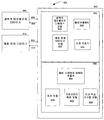
도 7 및 도 8은 에칭 스테이지 측정 시스템을 나타내는 예시적인 건축학상 도면이다. 도 7을 참조하면, 도 7은 광학적 메트롤로지 디바이스(704) 및 메트롤로지 프로세서(740)를 구비하는 에칭 스테이지 측정 시스템(700)을 나타내는 예시적인 건축상의 도면이다. 메트롤로지 프로세서(740)는 신호 평가기(720) 및 메트롤로지 데이터 추정기(750)를 포함할 수 있다. 광학적 메트롤로지 디바이스(704)는 광학적 방사 분광, 간섭계 또는 반사계 중 하나 이상의 조합과 같은 2 개 이상의 광학적 메트롤로지 디바이스일 수 있고, 기판(미도시)을 측정하고, 에칭 스테이지 측정(706)을 메트롤로지 프로세서(740)에 전송한다. 메트롤로지 프로세서(740)에 의한 측정을 처리한 후에, 예를 들어, 입사 각도 조정 또는 방위각 조정과 같은 조정 신호(708)가 메트롤로지 프로세서(740)로부터 광학적 메트롤로지 디바이스(704)로 전송될 수 있다. 메트롤로지 프로세서(740)는 국부적 프로세서, 원격 프로세서 또는 인터넷과 같은 네트워크를 통하여 액세스가능한 프로세서일 수 있다. 신호 평가기(720) 및 에칭 스테이지 데이터 추출기(754)는 프로세서(740)에 상주하거나 또는 프로세서(740)에 의한 실행에 대하여 이용할 수 있는 실행가능한 명령 또는 컴퓨터 코드의 형태일 수 있다. 신호 평가기(720)는 2 개 이상의 광학적 메트롤로지 디바이스를 모델화할 수 있는 광학적 메트롤로지 디바이스 모델(724)을 구비한다. 신호 평가기(720)의 다른 구성요소는 캘리브레이터(728) 및 신호 조정기(732)를 포함한다. 캘리브레이터(728)는 동일한 카테고리 또는 기술에서의 표준 디바이스와 비교되는 메트롤로지 디바이스에 이용되는 구성요소의 차이로 인해 메트롤로지 측정에 대한 조정을 결정하도록 구성된다. 신호 조정기(732)는 광학적 메트롤로지 디바이스(704)에 대하여 측정된 전자기 신호에서의 노이즈를 조정함으로써 신호를 향상시킨다.Figures 7 and 8 are illustrative architectural drawings illustrating an etching stage measurement system. Referring to FIG. 7, FIG. 7 is an exemplary architectural diagram showing an etching
도 7을 다시 참조하면, 메트롤로지 데이터 추정기(750)는 신호 평가기에 연결되며, 에칭 스테이지 데이터 추출기(754), 회귀 모듈(758), 라이브러리 매칭 모듈(762) 및 머신 학습 시스템 모듈(766)을 구비한다. 에칭 신호 데이터 추출기(754)는 신호 평가기(820)로부터 향상된 측정 신호를 이용하고, 회귀 모듈(758), 라이브러리 매칭 모듈(762) 및/또는 머신 학습 시스템 모듈(766) 중 하나 이상을 이용함으로써 에칭 스테이지값을 추출한다. 워크피스 상의 구조의 프로파일 데이터를 결정하기 위한 회귀 알고리즘의 사용에 대한 상세한 설명에 대해서는, 2004년 8월 31일자로 발행되며, "METHOD AND SYSTEM OF DYNAMIC LEARNING THROUGH A REGRESSION-BASED LIBRARY GENERATION PROCESS"로 명명되며, 그 전체가 여기에 참고로 포함되는 미국 특허 제6,785,638호를 참조한다. 워크피스 상의 구조의 프로파일 데이터를 결정하기 위한 라이브러리 알고리즘의 사용에 대한 상세한 설명에 대해서는, 2005년 9월 13일자로 발행되며, "GENERATION OF A LIBRARY OF PERIODIC GRATING DIFFRACTION SIGNALS"로 명명되며, 그 전체가 여기에 참고로 포함되는 미국 특허 제6,943,900호를 참조한다. 워크피스 상의 구조의 프로파일 데이터를 결정하기 위한 머신 학습 시스템 알고리즘의 사용에 대한 상세한 설명에 대해서는, 2010년 11월 9일자로 발행되며, "OPTICAL METROLOGY OF STRUCTURES FORMED ON SEMICONDUCTOR WAFERS USING MACHINE LEARNING SYSTEMS"으로 명명되며, 그 전체가 여기에 참고로 포함되는 미국 특허 제7,831,528호를 참조한다.7, the
도 8은 광학적 메트롤로지 디바이스(804), 에칭 센서 디바이스(810) 및 메트롤로지 프로세서(840)를 구비하는 에칭 스테이지 측정 시스템(800)을 나타내는 예시적인 건축상의 도면이다. 메트롤로지 프로세서(840)는 신호 평가기(820)와 메트롤로지 데이터 추정기(850)를 포함할 수 있다. 광학적 메트롤로지 디바이스(804)는, 하나 이상의 광학적 방사 분광, 간섭계 또는 반사계의 조합과 같은 2 개 이상의 광학적 메트롤로지 디바이스일 수 있으며, 기판(미도시)을 측정하고, 에칭 스테이지 측정값(806)을 메트롤로지 프로세서(840)에 전송한다. 메트롤로지 프로세서(840)에 대한 측정을 처리한 이후에, 예컨대 입사 각도 또는 방위각 조정과 같은 조정 신호(808)가 메트롤로지 프로세서(840)으로부터 광학적 메트롤로지 디바이스(804)로 전송될 수 있거나, 또는 예컨대 온도 및 압력 조정과 같은 조정 신호(814)가 에칭 센서 디바이스(810)로 전송될 수 있다. 메트롤로지 프로세서(840)는 국부적 프로세서, 원격 프로세서 또는 인터넷과 같은 네트워크를 통하여 액세스가능한 프로세서일 수 있다. 신호 평가기(820) 및 에칭 스테이지 데이터 추출기(854)는, 프로세서(840)에 상주하거나 또는 프로세서(840)에 의한 실행에 대하여 이용할 수 있는 실행가능한 명령 또는 컴퓨터 코드의 형태일 수 있다. 신호 평가기(820)는 2 개 이상의 광학적 메트롤로지 디바이스를 모델화할 수 있는 광학적 메트롤로지 디바이스 모델(824)과, 온도, 압력 또는 종 조성 센서 디바이스와 같은 2 개 이상의 에칭 센서 디바이스를 모델화할 수 있는 에칭 센서 디바이스 모델(836)을 구비한다. 신호 평가기(820)의 다른 구성요소는 캘리브레이터(828) 및 신호 조정기(832)를 포함한다. 캘리브레이터(828)는 동일한 카테고리 또는 기술에서의 표준 디바이스와 비교되는 메트롤로지 디바이스에 이용되는 구성요소의 차이로 인해 메트롤로지 측정에 대한 조정을 결정하도록 구성된다. 신호 조정기(832)는 광학적 메트롤로지 디바이스(804)에 대하여 측정된 전자기 신호 및/또는 에칭 센서 디바이스(810)로부터의 측정된 센서 신호(812)에서의 노이즈를 조정함으로써 신호를 향상시킨다.8 is an exemplary architectural diagram illustrating an etching
도 8을 다시 참조하면, 메트롤로지 데이터 추정기(850)는 신호 평가기에 연결되며, 에칭 스테이지 데이터 추출기(854), 회귀 모듈(858), 라이브러리 매칭 모듈(862) 및 머신 학습 시스템 모듈(866)을 구비한다. 에칭 신호 데이터 추출기(854)는 신호 평가기(820)로부터 향상된 측정 신호를 이용하고, 회귀 모듈(858), 라이브러리 매칭 모듈(862) 및/또는 머신 학습 시스템 모듈(866) 중 하나 이상을 이용함으로써 에칭 스테이지값을 결정한다. 워크피스 상의 구조의 프로파일 데이터를 결정하기 위한 회귀 알고리즘의 사용에 대한 상세한 설명에 대해서는, 2004년 8월 31일자로 발행되며, "METHOD AND SYSTEM OF DYNAMIC LEARNING THROUGH A REGRESSION-BASED LIBRARY GENERATION PROCESS"로 명명되며, 그 전체가 여기에 참고로 포함되는 미국 특허 제6,785,638호를 참조한다. 워크피스 상의 구조의 프로파일 데이터를 결정하기 위한 라이브러리 알고리즘의 사용에 대한 상세한 설명에 대해서는, 2005년 9월 13일자로 발행되며, "GENERATION OF A LIBRARY OF PERIODIC GRATING DIFFRACTION SIGNALS"로 명명되며, 그 전체가 여기에 참고로 포함되는 미국 특허 제6,943,900호를 참조한다. 워크피스 상의 구조의 프로파일 데이터를 결정하기 위한 머신 학습 시스템 알고리즘의 사용에 대한 상세한 설명에 대해서는, 2010년 11월 9일자로 발행되며, "OPTICAL METROLOGY OF STRUCTURES FORMED ON SEMICONDUCTOR WAFERS USING MACHINE LEARNING SYSTEMS"으로 명명되며, 그 전체가 여기에 참고로 포함되는 미국 특허 제7,831,528호를 참조한다.8, the
도 9는 본 발명의 일 실시형태에서의 실시간 에칭 스테이지 측정 시스템(900)에 대한 예시적인 흐름도를 나타낸다. 단계 905에서, 에칭 스테이지 측정 목표가 설정된다. 전술한 바와 같이, 에칭 스테이지 측정 목표는 정확도, 신뢰 간격, 측정 및 추출 시간(MAET) 목표, 반복성, 정밀도, 재현성, 전체 측정 불확실성(TMU), 소유권의 전체 비용 등을 포함할 수 있다. 일 실시형태에서, 예컨대 정확도, 측정 및 추출 시간, 및 반복성은 에칭 스테이지 측정 목표로서 이용된다. 또한, 에칭 스테이지 측정 목표는 0.97 이상으로 설정된 정확도, 3 밀리초 이하의 측정 및 추출 시간, 및 0.95 이상의 반복성 계수에 의해 명시될 수 있다. 다른 실시형태에서는, 정확도, 측정 및 추출 시간, 반복성, 그리고 예컨대 에칭 챔버의 온도 또는 에칭 챔버 내의 에천트 종의 양을 에칭 스테이지 측정 목표로서 이용한다. 단계 910에서, 실시간 에칭 스테이지 측정 시스템은, 도 4 내지 도 6과 관련하여 설명된 방법을 이용하고, 도 7 및 도 8과 관련하여 묘화되고 설명된 시스템을 이용하여 개발된다. 예를 들어, 에칭 스테이지 측정 시스템은 2 개 이상의 광학적 메트롤로지 디바이스 및 2 개 이상의 에칭 센서 디바이스를 이용하여 개발될 수 있다.FIG. 9 illustrates an exemplary flow diagram for a real-time etch
단계 915에서, 단계 910에서의 선택된 방법 및 시스템에 대한 광학적 메트롤로지 디바이스 및/또는 에칭 센서 디바이스를 이용하여 에칭 스테이지 측정을 획득한다. 단계 920에서, 에칭 스테이지 값은 입력으로서의 에칭 스테이지 측정 및 실시간 에칭 스테이지 측정 시스템을 이용하여 추출된다. 예를 들어, 에칭 스테이지 메트롤로지 측정은, OES 스펙트럼과 반사계 및 간섭계 측정과 같은 2 개 이상의 광학적 메트롤로지 측정을 포함할 수 있다. 또 다른 실시형태에서, 에칭 스테이지 측정은, 온도, 압력 또는 에칭 챔버에서의 에천트 종 농도와 같은 센서 데이터 및 2 개 이상의 광학적 메트롤로지 데이터를 포함할 수 있다.At
도 9를 다시 참조하면, 에칭 스테이지 값은 에칭 스테이지 측정 및 실시간 에칭 스테이지 측정 시스템을 이용하여 추출된다. 전술한 바와 같이, 에칭 스테이지 값은, 에칭된 층 또는 층들의 두께이거나, 또는 에칭되고 있는 기판의 2 개 이상의 층에서의 에칭 타겟의 퍼센트일 수 있으며, 그 타겟은 애플리케이션의 레시피에 기초한다. 에칭 스테이지 값의 추출은, 도 4 내지 도 6과 관련하여 설명된 방법 및 에칭 스테이지 측정을 이용하고 그리고 도 7 또는 도 8과 관련하여 묘화되고 설명된 시스템을 이용하여 수행된다. 단계 925에서, 추출된 스테이지 값은, 에칭 프로세싱이 완료되었는지를 판정하기 위하여 에칭 타겟과 비교된다. 에칭 프로세싱이 완료되면, 단계 930에서, 메트롤로지 프로세서(도 2, 216)에 에칭 완료 신호를 전송한다.Referring back to FIG. 9, the etching stage values are extracted using an etching stage measurement and a real time etching stage measurement system. As discussed above, the etch stage value may be the thickness of the etched layer or layers, or it may be a percentage of the etch target in two or more layers of the substrate being etched, the target being based on the recipe of the application. The extraction of the etching stage value is performed using the method and etching stage measurement described in connection with FIGS. 4-6 and using the system depicted and described with reference to FIG. 7 or FIG. In
에칭 처리가 완료되지 않으면, 단계 935에서, 에칭 스테이지 값은 에칭 처리의 경과된 지속 시간 동안의 설정 범위와 비교된다. 에칭 스테이지 값이 설정 범위 내에 있지 않으면, 경고 신호는 단계 940 메트롤로지 프로세서(도 2, 216)에 송신된다. 기판을 가로지는 에칭 스테이지 값을 설정 범위와 비교하여, 전체 기판이 레시피당 또는 다른 설정 기준으로서 에칭되고 있다는 것을 보증한다. 기판 전체에 걸친 에칭 처리가 설정 범위 내에 있지 않으면, 단계 940에서 경고 신호가 송신된다. 단계 945에서, 기판을 가로지르는 에칭이 설정 범위 내에 있지 않으면, 단계 940에서 경고 신호가 송신된다. 실제 추출 시간 및 참조 에칭 스테이지 데이터는 단계 955에서 획득된다. 실제 측정 및 추출 시간은 메트롤로지 프로세서(도 2, 216)에서 유지되는 타이머에 의해 기록될 수 있다. 에칭 스테이지 측정 목표는 추출된 에칭 스테이지 값, 실제 측정 및 추출 시간 및 참조 에칭 스테이지 데이터를 이용하여 계산되며, 단계 905에서 설정된 대응하는 에칭 스테이지 측정 목표와 비교된다. 전술한 바와 같이, 레퍼런스 에칭 스테이지 데이터는, 도쿄 엘렉트론 주식회사 및 KLA-Tencor 가부시키가이샤에 의해 소유된 AcuShapeTM와 같은, SEM, AFM, 또는 광 디지털 프로필로메트리를 이용하는 것 등의 기준 측정 시스템을 이용함으로써 획득될 수 있다. 에칭 스테이지 측정 목표가 충족되지 않으면, 단계 960에서 경고 신호는 메트롤로지 프로세서(도 2, 216)에 송신된다. 이와 달리, 처리 단계 915 내지 960는, 단계 925에서 판정될 때, 에칭 처리가 완료될 때 까지 반복된다.If the etching process is not completed, in
도 10, 11 및 12는 하나 이상의 광학 메트롤로지 디바이스와 에칭 센서 디바이스의 여러 가지 조합을 이용하여, 에칭 스테이지 측정 시스템에 연결된 플라즈마 처리 시스템을 구비하는 예시적인 에칭 시스템을 나타내는 건축상의 도면이다. 도 10을 참조하면, 도 10은 하나 이상의 광학적 메트롤로지 디바이스를 이용하여 에칭 스테이지 시스템(1008)에 연결된 플라즈마 시스템(1004)을 구비하는 예시적인 에칭 시스템(1000)을 나타내는 건축상의 도면이다. 플라즈마 프로세싱 시스템(1004)은 선택적으로 기판(1025)에 대향하는 상부 전극(1052)에 연결된 직류(DC) 전원(1050)을 구비한다. 상부 전극(1052)은 전극판을 구비할 수도 있다. 전극판은 실리콘 함유 전극판을 구비할 수 있다. 또한, 전극판은 도핑된 실리콘 전극판을 구비할 수 있다. DC 전원은 가변 DC 전원을 포함할 수 있다. 부가적으로, DC 전원은 바이폴라 DC 전원을 포함할 수 있다. DC 전원(1050)은 DC 전원(1050)의 극성, 전류, 전압 또는 온/오프 상태이거나 이들의 임의의 조합을 모니터링, 조정 또는 제어하도록 구성된 시스템을 더 포함할 수 있다. 일단 플라즈마가 형성되면, DC 전원(1050)은 발리스틱(ballistic) 전자빔의 형성을 용이하게 한다. 전기 필터는 DC 전원(1050)으로부터 무선 주파수(RF) 파워를 분리하는데 이용될 수 있다.10, 11, and 12 are architectural diagrams illustrating an exemplary etch system having a plasma processing system coupled to an etch stage measurement system using various combinations of one or more optical metrology devices and etch sensor devices. 10, there is shown an architectural view of an
예컨대, DC 전원(1050)에 의해 상부 전극(1052)에 인가된 DC 전압은 대략 -2000 볼트(V) 내지 대략 1000 V의 범위에 이른다. 바람직하기로는, DC 전압의 절대값은 대략 100 V 이상의 값을 가지며, 더욱 바람직하기로는, DC 전압의 절대값은 대략 500 V의 이상의 값을 가진다. 부가적으로, DC 전압은 음의 극성을 가지는 것이 바람직하다. 또한, DC 전압은 상부 전극(1052)의 표면에 생성된 자기 바이어스 전압보다 더 큰 절대값을 가지는 음의 전압이다. 기판 홀더(1020)와 대향하는 상부 전극(1052)의 표면은 실리콘 함유 재료로 이루어질 수 있다.For example, the DC voltage applied to the
진공 펌프 시스템(1030)은 초당 5000 리터(및 그 이상)까지 펌핑 속도를 낼 수 있는 터보 분자 진공 펌프(TMP) 및 챔버 압력을 스로틀링하는 게이트 밸브를 포함할 수 있다. 건식 플라즈마 에칭에 이용되는 종래의 플라즈마 프로세싱 디바이스에 있어서, 초당 1000 내지 3000 리터의 TMP를 사용할 수 있다. TMP는 일반적으로 대략 50 mTorr 미만의 낮은 압력 프로세싱에 이용될 수 있다. 높은 압력 프로세싱에서는(즉, 대략 100 mTorr 보다 큼), 기계적 부스터 펌프 및 건식 러핑 펌프를 이용할 수 있다. 또한, 챔버 압력을 모니터링하기 위한 디바이스(미도시)는 플라즈마 프로세싱 챔버(1010)에 연결될 수 있다. 압력 측정 디바이스는, 예컨대 MKS Instruments, Inc. (Andover, MA)로부터 상업적으로 입수가능한 Type 628B 바라트론 절대 커패시턴스 마노미터일 수 있다.
도 10을 계속 참조하면, 플라즈마 프로세싱 시스템(1004)은, 플라즈마 프로세싱 시스템(1004)으로의 입력을 전달하고 활성화시킬 뿐만 아니라 플라즈마 프로세싱 시스템(1004)으로부터의 출력을 모니터하기에 충분한 제어 전압을 생성할 수 있는 마이크로프로세서, 메모리 및 디지털 I/O 포트를 구비하는 제어기(1090)를 더 포함한다. 또한, 제어기(1090)는, RF 발생기(100), 임피던스 매칭 네트워크(1042), 옵션적인 DC 전원(1050), 가스 분사(injection) 시스템(미도시), 진공 펌핑 시스템(1030)뿐만 아니라 후면 가스 전달 시스템(미도시), 기판/기판 홀더 온도 제어 시스템(미도시) 및/또는 전자기 클램핑 시스템(미도시)에 연결될 수 있고, 이들과 정보를 교환할 수 있다. 메모리에 저장된 프로그램은 박막 에칭 방법을 수행하기 위하여 프로세스 레시피에 따라서 플라즈마 프로세싱 시스템(1004)의 전술한 구성요소로의 입력을 활성화하는데 이용될 수 있다. 제어기(1090)의 일례는 텍사스주 오스틴 소재의 델 코포레이션으로부터 입수가능한 DELL PRECISION WORKSTATION 610TM이다. 제어기(1090)는 플라즈마 프로세싱 시스템(1004)에 관하여 국부적으로 위치될 수 있거나 또는 인터넷 또는 인트라넷을 통하여 플라즈마 프로세싱 시스템(1004)에 관하여 원격으로 위치될 수 있다. 이에 따라, 제어기(1090)는 직접 접속, 인트라넷 또는 인터넷 중 적어도 하나를 이용하여 플라즈마 프로세싱 시스템(1004)과 데이터를 교환할 수 있다. 제어기(1090)는 커스터머 사이트(즉, 디바이스 제조자 등)에서 인트라넷에 연결될 수 있거나 또는 벤더 사이트(즉, 장비 제조자)에서 인트라넷에 연결될수 있다. 또한, 또 다른 컴퓨터(즉, 제어기, 서버 등)는 직접 접속, 인트라넷 또는 인터넷 중 적어도 하나를 통하여 데이터를 교환하기 위하여 제어기(1090)에 액세스할 수 있다.10, the
에칭 스테이지 측정 시스템(1008)은 2 개 이상의 광학 메트롤로지 디바이스를 이용한다. 특히 도 10에 있어서, OES 디바이스(1070)는 기판(1025)과 상부 전극(1052) 사이의 프로세싱 영역(1015)으로부터 광학적 방사를 측정하는 위치에서 플라즈마 프로세싱 챔버(1010)에 연결된다. 게다가, 광학적 메트롤로지 디바이스(1060)의 또 다른 세트는 플라즈마 프로세싱 챔버(1010)의 맨 위에 배치된다. 4개의 광학적 메트롤로지 디바이스가 도시되어 있지만, 광학적 메트롤로지 디바이스의 많은 다른 대안물 및 상이한 구성이, 복수의 광학적 메트롤로지 디바이스를 이용하여 설계 목표를 구현하기 위하여 배치될 수 있다. 4개의 광학적 메트롤로지 디바이스는 분광 반사율계 디바이스 또는 간섭 측정 디바이스일 수 있다. 2 개 이상의 광학적 메트롤로지 디바이스 예컨대 OES 디바이스(1070) 및 광학적 메틀롤로지 디바이스(1060)의 세트로부터의 측정은 메트롤로지 프로세서(미도시)에 전송되고, 신호 평가기(도 7, 720)(미도시) 및 메트롤로지 데이터 추정기(도 7, 750)(미도시)에 의해 프로세싱되며, 여기서 에칭 스테이지 값이 추출된다.The etching
도 11은 에칭 스테이지 측정 시스템(1008)이 하나 이상의 광학적 메트롤로지 디바이스 및 에칭 센서 디바이스(1064)를 이용하는 점을 제외하고, 도 10의 예시적인 에칭 시스템(1000)과 유사하다. 전술한 바와 같이, 프로세스 센서 디바이스 예컨대 에천트의 양을 측정하는 에칭 센서 디바이스(1064)는, 에칭 스테이지에 실질적으로 상관된 측정에 관하여 선택된다. 일 실시형태에서, 에칭 스테이지와 가장 높은 상관관계를 가지는 에칭 프로세스 센서 디바이스가 선택된다. 적어도 하나의 프로세스 센서 디바이스는, 이들의 상호 관계를 식별하기 위하여 프로세스 데이터의 세트, 메트롤로지 데이터(회절 신호) 및 프로세스 퍼포먼스 데이터를 이용하는 다변량 해석을 이용하여 선택될 수 있다. 특히 도 11에 있어서, OES 디바이스(1070)는 기판(1025)과 상부 전극(1052) 사이의 프로세싱 영역(1015)으로부터의 광학적 방사를 측정하기 위한 위치에서 플라즈마 프로세싱 챔버(1010)에 연결된다. 또 다른 실시형태에서, 도시된 4개의 광학적 메트롤로지 디바이스와 같은 광학적 메트롤로지 디바이스(1060)의 또 다른 세트는, 플라즈마 프로세싱 챔버(1010)의 맨 위에 배치된다. 4개의 광학적 메트롤로지 디바이스는 분광 반사율계 디바이스 또는 간섭 측정 디바이스일 수 있다. 2 개 이상의 광학적 메트롤로지 디바이스 예컨대 OES 디바이스(1070) 및 광학적 메트롤로지 디바이스(1060)의 세트로부터 측정과 센서 디바이스(1064)로부터의 측정은, 메트롤로지 프로세서(미도시)에 전송되어 신호 평가기(도 8, 820)(미도시) 및 메트롤로지 데이터 추정기(도 8, 850)(미도시)에 의해 프로세싱되고, 여기서 에칭 스테이지 값이 추출된다.FIG. 11 is similar to the
도 12는 에칭 스테이지 측정 시스템(1008)이 하나 이상의 광학적 메트롤로지 디바이스 및 복수의 에칭 센서 디바이스(1064 및 1068)를 이용하는 점을 제외하고, 도 11의 예시적인 에칭 시스템(1100)과 유사하다. 전술한 바와 같이, 에칭 스테이지와 실질적으로 상관되는 측정에 관한 프로세스 센서 디바이스가 선택된다. 일 실시형태에서, 에칭 스테이지와 가장 높은 상관관계를 가지는 에칭 프로세스 센서가 선택된다. 프로세스 센서 디바이스의 선택은, 이들의 상호 관계를 식별하기 위하여 프로세스 데이터의 세트, 메트롤로지 데이터(회절 신호) 및 프로세스 퍼포먼스 데이터를 이용하는 다변량 분석을 이용하여 행해질 수 있다. 특히 도 12에 있어서, OES 디바이스(1070)는 기판(1025)과 상부 전극(1052) 사이의 프로세싱 영역(1015)으로부터의 광학적 방사를 측정하기 위한 위치에서 플라즈마 프로세싱 챔버(1010)에 연결된다. 또 다른 실시형태에서, 도시된 4개의 광학적 메트롤로지 디바이스와 같은 광학적 메트롤로지 디바이스(1060)의 또 다른 세트가 플로즈마 프로세싱 시스템(1010)의 맨 위에 배치된다. 4개의 광학적 메트롤로지 디바이스는 분광 반사계 디바이스 또는 간섭 측정 디바이스일 수 있다. 2 개 이상의 광학적 메트롤로지 디비이스 예컨대 OES 디바이스(1070) 및 광학적 메트롤로지 디바이스(1060)의 세트로부터의 측정과 복수의 센서 디바이스로부터의 측정은 메트롤로지 프로세서(미도시)에 전송되어, 신호 평가기(도 8, 820)(미도시) 및 메트롤로지 데이터 추정기(도 8, 850)(미도시)에 의해 프로세싱되며, 여기서 에칭 스테이지 값이 추출된다.12 is similar to the
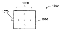
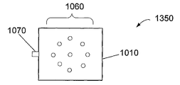
도 13a는 광학적 방사 분광(OES) 디바이스(1070)와, 광학적 분광 및/또는 간섭 측정 툴에 대한 플라즈마 프로세싱 챔버(1010)의 상부의 광학적 메트롤로지 디바이스(1060)에 대한 복수의 뷰포트를 가진 예시적인 에칭 시스템(1300)의 평면도를 나타낸다. OES 디바이스(1070)는, 플라즈마 프로세싱 챔버의 다른 구성요소들이 광학적 방사 신호의 방해받지 않은 측정을 허용하는 위치에 배치될 수 있고, 다른 광학적 메트롤로지 디바이스(1060)의 배열이 도시된 바와 같이 배치될 수 있다. 이러한 광학적 메트롤로지 디바이스로부터의 회절된 전자기 에너지의 측정은, 애플리케이션 레시피에 따라서 웨이퍼의 여러 가지 사이트의 에칭이 진행되고 있는지를 판정하는데 이용된다. 대안적으로, 광학적 메트롤로지 디바이스의 수는, 예컨대 다른 구성에 배열되는 5, 7, 9 또는 11 개의 광학적 메트롤로지 디바이스를 이용하여 증가될 수 있다. 예를 들어, 도 13b에서, 9개의 광학적 메트롤로지 디바이스를 가진 예시적인 에칭 시스템(1350)은 도시된 바와 같은 구성에 배열 될 수 있다. 광학적 메트롤로지 디바이스의 특정수 및 구성은, 에칭 스테이지 측정 시스템에 의해 측정되도록 계획된 반도체 애플리케이션의 범위에서의 지식 및 경험에 기초하여 결정된다. 13A illustrates an example with an optical emission spectroscopy (OES)
예시적인 실시형태들을 설명하였지만, 본 발명의 사상 및/또는 범위를 벗어나지 않고 여러 가지 변경이 행해질 수 있다. 따라서, 본 발명은 도면들에 도시되고 앞에서 설명한 특정 형태로 한정되는 것으로 구성되어서는 안 된다. 따라서, 모든 이러한 변경은 본 발명의 범위 내에 포함되도록 의도된다.Although illustrative embodiments have been described, various modifications may be made without departing from the spirit and / or scope of the invention. Accordingly, the present invention should not be construed as limited to the specific forms shown in the drawings and described above. Accordingly, all such modifications are intended to be included within the scope of the present invention.
Claims (10)
기판을 처리하기 위한 제1 제조 클러스터로서,
상기 기판 상의 하나 이상의 층을 에칭하도록 구성되는 에칭 프로세스 툴을 포함하고, 상기 에칭 프로세스 툴은, 에칭 챔버, 계측 뷰포트, 제어 장치 및 하나 이상의 에칭 프로세스 파라미터를 갖는, 제1 제조 클러스터와,
에칭 단계를 측정하고, 2 이상의 에칭 단계 측정 목표값에 합치시키도록 구성되는 에칭 단계 측정 시스템으로서,
상기 에칭 프로세스 툴에 결합되어, 상기 에칭 챔버로부터의 전자기 에너지를 측정하도록 구성된 제1 광학 계측 장치,
상기 에칭 프로세스 툴에 접속되고, 상기 기판의 하나 이상의 위치에 조사하고, 상기 조사된 하나 이상의 위치로부터의 회절 신호를 측정하도록 구성된, 제2 광학 계측 장치,
상기 에칭 프로세스 툴에 결합되고, 상기 하나 이상의 에칭 프로세스 파라미터 중 하나의 프로세스 파라미터를 측정하도록 구성되는, 에칭 센서 장치와,
상기 에칭 프로세스 툴, 상기 제1 광학 계측 장치 및 상기 제2 광학 계측 장치에 결합된 프로세서
를 갖는, 에칭 단계 측정 시스템
을 포함하고,
상기 프로세서는, 상기 제1 및 제2 광학 계측 장치와 상기 에칭 센서 장치로부터의 측정된 프로세스 파라미터로부터, 실제의 에칭 단계 데이터에 대한, 상기 측정된 전자기 에너지의 상관관계 알고리즘을 확립하도록 구성되고,
상기 제1 광학 계측 장치 및 상기 제2 광학 계측 장치로부터의 에칭 단계 측정값과, 실제의 에칭 단계 데이터에 대한 에칭 단계 측정값의 상관관계를 이용하여, 에칭 단계값을 도출하고,
2 이상의 에칭 단계 측정 목표값과 비교하여, 계산된 2 이상의 에칭 단계 측정 목표값이 합치하지 않는 경우에는, 제1 및 제2 광학 계측 장치를 수정하고 상기 상관관계 알고리즘을 조절하는 것과 상기 측정된 전자파 에너지의 노이즈를 조절하는 것 중 적어도 하나를 수행함으로써, 상기 에칭 단계 측정값이 강화되고, 상기 상관관계 알고리즘을 확립하는 것이 반복되고,
상기 2 이상의 에칭 단계 측정 목표값이 합치할 때까지, 상기 에칭 단계값을 도출하고, 상기 계산된 2 이상의 에칭 단계 측정 목표값을 상기 2 이상의 에칭 단계 측정 목표값과 비교하며, 상기 제1 및 제2 광학 계측 장치를 수정하고 상기 상관관계 알고리즘을 조절하는 것과 상기 측정된 전자기 에너지의 노이즈를 조절하는 것 중 적어도 하나를 수행함으로써, 상기 에칭 단계 측정값이 강화되고,
상기 시스템은, 또한,
상기 제1 제조 클러스터 및 상기 에칭 단계 측정 시스템에 결합된 제2 제조 클러스터를 포함하고,
상기 제2 제조 클러스터는, 하나 이상의 장치 설정과 하나 이상의 프로세스 파라미터를 가지고, 적어도 하나의 상기 도출된 에칭 단계값에 기초하여, 상기 하나 이상의 장치 설정과 상기 하나 이상의 에칭 프로세스 파라미터 중 적어도 하나를 조절하는, 시스템.A system for controlling a manufacturing cluster, the system comprising:
CLAIMS 1. A first production cluster for processing a substrate,
An etch process tool configured to etch at least one layer on the substrate, the etch process tool comprising: a first fabrication cluster having an etch chamber, a metrology viewport, a control device and at least one etch process parameter;
An etch step measurement system configured to measure an etch step and conform to at least two etch step measurement target values,
A first optical metrology apparatus coupled to the etch process tool, the first optical metrology apparatus configured to measure electromagnetic energy from the etch chamber,
A second optical metrology apparatus connected to the etch process tool and configured to illuminate at least one location of the substrate and to measure a diffraction signal from the irradiated one or more locations,
An etch sensor device coupled to the etch process tool and configured to measure a process parameter of one of the one or more etch process parameters;
The etching process tool, the processor coupled to the first optical metrology apparatus and the second optical metrology apparatus,
With an etching step measuring system
/ RTI >
Wherein the processor is configured to establish a correlation algorithm of the measured electromagnetic energy for actual etch step data from measured process parameters from the first and second optical metrology apparatus and the etch sensor apparatus,
Deriving an etching step value using a correlation between an etching step measurement value from the first optical measuring apparatus and the second optical measuring apparatus and an etching step measurement value with respect to actual etching step data,
Modifying the first and second optical measuring devices and adjusting the correlation algorithm when the calculated two or more etching step measurement target values do not match, compared to two or more etching step measurement target values, And adjusting the noise of the energy, the etching step measurements are enhanced, and establishing the correlation algorithm is repeated,
Deriving the etching step value until the two or more etching step measurement target values agree with each other, comparing the calculated two or more etching step measurement target values with the two or more etching step measurement target values, 2 By performing at least one of modifying the optical metrology device and adjusting the correlation algorithm and adjusting the noise of the measured electromagnetic energy, the etch step measurement is enhanced,
The system may further comprise:
A second fabrication cluster coupled to the first fabrication cluster and the etch step measurement system,
Wherein the second fabrication cluster has one or more device settings and one or more process parameters and adjusts at least one of the one or more device settings and the one or more etch process parameters based on the at least one derived etch step value , system.
상기 방법은:
2 이상의 에칭 단계 측정 목표값을 선택하는 단계와;
상기 2 이상의 에칭 단계 측정 목표값을 설정하는 단계와;
선택된 2 이상의 광학 계측 장치 및 선택된 에칭 프로세스 센서 장치를 이용하여 에칭 단계 측정값을 얻는 단계로서, 상기 에칭 프로세스 센서 장치는 상기 하나 이상의 에칭 프로세스 파라미터의 하나의 프로세스 파라미터를 측정하도록 구성되는 단계와;
하나 이상의 표준 측정 기술을 이용하여, 상기 에칭 단계 측정값의 각각에 대한 실제의 에칭 단계 데이터를 얻는 단계와;
에칭 단계 측정값과 실제의 에칭 단계 데이터의 상관관계를 확립하는 단계와;
상기 확립된 상관관계 알고리즘을 이용하여, 선택된 2 이상의 광학 계측 장치 및 상기 선택된 에칭 프로세스 센서 장치를 이용하여 얻어지는 에칭 단계 측정값을 이용하여, 에칭 단계값을 도출하는 단계와;
상기 에칭 단계값을 상기 제조 클러스터에 전달하는 단계와;
상기 전달된 에칭 단계 데이터에 기초하여, 장치 설정과 프로세스 파라미터 중 적어도 하나를 변경하는 단계,
를 포함하는 방법.CLAIMS What is claimed is: 1. A method for controlling a fabrication cluster for processing a substrate with an etch process, the fabrication cluster having a device set point and at least one etch process parameter,
The method comprising:
Selecting at least two etch step measurement target values;
Setting the at least two etching step measurement target values;
Obtaining an etch step measurement using the selected two or more optical metrology devices and a selected etch process sensor device, wherein the etch process sensor device is configured to measure one process parameter of the at least one etch process parameter;
Obtaining actual etch step data for each of the etch step measurements using one or more standard measurement techniques;
Establishing a correlation between the etching step measurement and actual etching step data;
Using the established correlation algorithm to derive an etch step value using etch step measurements obtained using the selected two or more optical metrology devices and the selected etch process sensor device;
Transferring the etching step value to the manufacturing cluster;
Changing at least one of a device setting and a process parameter based on the transferred etching step data,
≪ / RTI >
Applications Claiming Priority (3)
| Application Number | Priority Date | Filing Date | Title |
|---|---|---|---|
| US13/029,349 | 2011-02-17 | ||
| US13/029,349 US8193007B1 (en) | 2011-02-17 | 2011-02-17 | Etch process control using optical metrology and sensor devices |
| PCT/US2012/025746 WO2012112959A1 (en) | 2011-02-17 | 2012-02-17 | Etch process control using optical metrology and sensor devices |
Related Parent Applications (1)
| Application Number | Title | Priority Date | Filing Date |
|---|---|---|---|
| KR1020137024624A Division KR20140006039A (en) | 2011-02-17 | 2012-02-17 | Etch process control using optical metrology and sensor devices |
Publications (1)
| Publication Number | Publication Date |
|---|---|
| KR20170107094A true KR20170107094A (en) | 2017-09-22 |
Family
ID=46148020
Family Applications (2)
| Application Number | Title | Priority Date | Filing Date |
|---|---|---|---|
| KR1020177025199A KR20170107094A (en) | 2011-02-17 | 2012-02-17 | Etch process control using optical metrology and sensor devices |
| KR1020137024624A KR20140006039A (en) | 2011-02-17 | 2012-02-17 | Etch process control using optical metrology and sensor devices |
Family Applications After (1)
| Application Number | Title | Priority Date | Filing Date |
|---|---|---|---|
| KR1020137024624A KR20140006039A (en) | 2011-02-17 | 2012-02-17 | Etch process control using optical metrology and sensor devices |
Country Status (5)
| Country | Link |
|---|---|
| US (1) | US8193007B1 (en) |
| JP (1) | JP6019043B2 (en) |
| KR (2) | KR20170107094A (en) |
| TW (1) | TWI464818B (en) |
| WO (1) | WO2012112959A1 (en) |
Families Citing this family (15)
| Publication number | Priority date | Publication date | Assignee | Title |
|---|---|---|---|---|
| US8445296B2 (en) * | 2011-07-22 | 2013-05-21 | Taiwan Semiconductor Manufacturing Company, Ltd. | Apparatus and methods for end point determination in reactive ion etching |
| US9287097B2 (en) * | 2011-11-30 | 2016-03-15 | Sony Corporation | Predicting ultraviolet ray damage with visible wavelength spectroscopy during a semiconductor manufacturing process |
| US9875946B2 (en) * | 2013-04-19 | 2018-01-23 | Kla-Tencor Corporation | On-device metrology |
| KR102242414B1 (en) | 2013-10-02 | 2021-04-21 | 에이에스엠엘 네델란즈 비.브이. | Methods & apparatus for obtaining diagnostic information relating to an industrial process |
| US10217681B1 (en) * | 2014-08-06 | 2019-02-26 | American Air Liquide, Inc. | Gases for low damage selective silicon nitride etching |
| US20160240366A1 (en) * | 2015-02-17 | 2016-08-18 | Infineon Technologies Ag | Processing of Semiconductor Devices |
| US10386829B2 (en) * | 2015-09-18 | 2019-08-20 | Kla-Tencor Corporation | Systems and methods for controlling an etch process |
| US10192763B2 (en) * | 2015-10-05 | 2019-01-29 | Applied Materials, Inc. | Methodology for chamber performance matching for semiconductor equipment |
| US10372114B2 (en) * | 2016-10-21 | 2019-08-06 | Kla-Tencor Corporation | Quantifying and reducing total measurement uncertainty |
| CN110383428B (en) * | 2017-03-10 | 2023-04-04 | 三菱电机株式会社 | Semiconductor manufacturing apparatus and semiconductor manufacturing method |
| US10784174B2 (en) * | 2017-10-13 | 2020-09-22 | Lam Research Corporation | Method and apparatus for determining etch process parameters |
| US11164768B2 (en) * | 2018-04-27 | 2021-11-02 | Kla Corporation | Process-induced displacement characterization during semiconductor production |
| JP2020181959A (en) | 2019-04-26 | 2020-11-05 | 東京エレクトロン株式会社 | Learning method, management device and management program |
| JP7413081B2 (en) * | 2020-02-28 | 2024-01-15 | 東京エレクトロン株式会社 | Substrate processing system |
| US20230163001A1 (en) * | 2021-11-23 | 2023-05-25 | Applied Materials, Inc. | Method to eliminate first wafer effects on semiconductor process chambers |
Family Cites Families (21)
| Publication number | Priority date | Publication date | Assignee | Title |
|---|---|---|---|---|
| US5288367A (en) | 1993-02-01 | 1994-02-22 | International Business Machines Corporation | End-point detection |
| US5658423A (en) | 1995-11-27 | 1997-08-19 | International Business Machines Corporation | Monitoring and controlling plasma processes via optical emission using principal component analysis |
| US5862060A (en) | 1996-11-22 | 1999-01-19 | Uop Llc | Maintenance of process control by statistical analysis of product optical spectrum |
| US6943900B2 (en) | 2000-09-15 | 2005-09-13 | Timbre Technologies, Inc. | Generation of a library of periodic grating diffraction signals |
| US6785638B2 (en) | 2001-08-06 | 2004-08-31 | Timbre Technologies, Inc. | Method and system of dynamic learning through a regression-based library generation process |
| US7216045B2 (en) | 2002-06-03 | 2007-05-08 | Timbre Technologies, Inc. | Selection of wavelengths for integrated circuit optical metrology |
| US6979578B2 (en) | 2002-08-13 | 2005-12-27 | Lam Research Corporation | Process endpoint detection method using broadband reflectometry |
| US7352478B2 (en) | 2002-12-20 | 2008-04-01 | International Business Machines Corporation | Assessment and optimization for metrology instrument |
| US20040267397A1 (en) | 2003-06-27 | 2004-12-30 | Srinivas Doddi | Optical metrology of structures formed on semiconductor wafer using machine learning systems |
| US7158221B2 (en) * | 2003-12-23 | 2007-01-02 | Applied Materials, Inc. | Method and apparatus for performing limited area spectral analysis |
| US7065423B2 (en) * | 2004-07-08 | 2006-06-20 | Timbre Technologies, Inc. | Optical metrology model optimization for process control |
| KR20060005830A (en) | 2004-07-14 | 2006-01-18 | 삼성전자주식회사 | Printed circuit board including integrated slot |
| US20060112796A1 (en) | 2004-11-30 | 2006-06-01 | Chang-Ying Chen | Screwdriver with teethed head |
| US7467064B2 (en) | 2006-02-07 | 2008-12-16 | Timbre Technologies, Inc. | Transforming metrology data from a semiconductor treatment system using multivariate analysis |
| US7596422B2 (en) * | 2007-01-12 | 2009-09-29 | Tokyo Electron Limited | Determining one or more profile parameters of a structure using optical metrology and a correlation between profile models and key profile shape variables |
| CN101675495B (en) * | 2007-02-02 | 2011-12-14 | 雷克萨斯研究有限公司 | Method and apparatus for measuring process parameters of a plasma etch process |
| US7591600B2 (en) * | 2007-02-23 | 2009-09-22 | Tokyo Electron Limited | Method and system for monitoring photolithography processing based on a batch change in light sensitive material |
| US7742177B2 (en) | 2008-01-22 | 2010-06-22 | Tokyo Electron Limited | Noise-reduction metrology models |
| US7589845B1 (en) * | 2008-03-27 | 2009-09-15 | Tokyo Electron Limited | Process control using an optical metrology system optimized with signal criteria |
| US7761250B2 (en) | 2008-06-18 | 2010-07-20 | Tokyo Electron Limited | Optical metrology system optimized with design goals |
| US8173451B1 (en) * | 2011-02-16 | 2012-05-08 | Tokyo Electron Limited | Etch stage measurement system |
-
2011
- 2011-02-17 US US13/029,349 patent/US8193007B1/en active Active
-
2012
- 2012-02-17 KR KR1020177025199A patent/KR20170107094A/en not_active Application Discontinuation
- 2012-02-17 KR KR1020137024624A patent/KR20140006039A/en active Application Filing
- 2012-02-17 JP JP2013554662A patent/JP6019043B2/en active Active
- 2012-02-17 WO PCT/US2012/025746 patent/WO2012112959A1/en active Application Filing
- 2012-02-17 TW TW101105282A patent/TWI464818B/en active
Also Published As
| Publication number | Publication date |
|---|---|
| TWI464818B (en) | 2014-12-11 |
| US8193007B1 (en) | 2012-06-05 |
| TW201241949A (en) | 2012-10-16 |
| JP2014514727A (en) | 2014-06-19 |
| KR20140006039A (en) | 2014-01-15 |
| WO2012112959A1 (en) | 2012-08-23 |
| JP6019043B2 (en) | 2016-11-02 |
Similar Documents
| Publication | Publication Date | Title |
|---|---|---|
| US8193007B1 (en) | Etch process control using optical metrology and sensor devices | |
| US8173451B1 (en) | Etch stage measurement system | |
| JP7269296B2 (en) | Method and etching system | |
| US10002804B2 (en) | Method of endpoint detection of plasma etching process using multivariate analysis | |
| CN108281346B (en) | Method for feature extraction from a time series of spectra to control process end points | |
| JP3708031B2 (en) | Plasma processing apparatus and processing method | |
| KR101046918B1 (en) | Method and system for monitoring the etching process | |
| US7972483B2 (en) | Method of fault detection for material process system | |
| TWI528452B (en) | Plasma processing device and plasma processing method | |
| JP2006074067A (en) | Plasma treatment apparatus and method | |
| TWI773529B (en) | Plasma processing device and plasma processing method | |
| JP4660091B2 (en) | Material processing system and method for characterizing material processing system | |
| US8173450B1 (en) | Method of designing an etch stage measurement system | |
| KR20230118990A (en) | Machine-learning of multi-step semiconductor manufacturing processes | |
| JP4344674B2 (en) | Plasma processing equipment | |
| WO2022256194A1 (en) | In situ sensor and logic for process control | |
| US20030082838A1 (en) | Method and system for monitoring a semiconductor wafer plasma etch process | |
| Barna et al. | In Situ Metrology |
Legal Events
| Date | Code | Title | Description |
|---|---|---|---|
| A107 | Divisional application of patent | ||
| E902 | Notification of reason for refusal | ||
| AMND | Amendment | ||
| E601 | Decision to refuse application | ||
| E601 | Decision to refuse application | ||
| E801 | Decision on dismissal of amendment |