KR20170105480A - Spin on Hard-mask Material - Google Patents
Spin on Hard-mask Material Download PDFInfo
- Publication number
- KR20170105480A KR20170105480A KR1020177012083A KR20177012083A KR20170105480A KR 20170105480 A KR20170105480 A KR 20170105480A KR 1020177012083 A KR1020177012083 A KR 1020177012083A KR 20177012083 A KR20177012083 A KR 20177012083A KR 20170105480 A KR20170105480 A KR 20170105480A
- Authority
- KR
- South Korea
- Prior art keywords
- resin
- organic sulfonic
- composition
- sulfonic acids
- spin
- Prior art date
Links
- 239000000463 material Substances 0.000 title description 20
- 239000000203 mixture Substances 0.000 claims abstract description 63
- XMWRBQBLMFGWIX-UHFFFAOYSA-N C60 fullerene Chemical class C12=C3C(C4=C56)=C7C8=C5C5=C9C%10=C6C6=C4C1=C1C4=C6C6=C%10C%10=C9C9=C%11C5=C8C5=C8C7=C3C3=C7C2=C1C1=C2C4=C6C4=C%10C6=C9C9=C%11C5=C5C8=C3C3=C7C1=C1C2=C4C6=C2C9=C5C3=C12 XMWRBQBLMFGWIX-UHFFFAOYSA-N 0.000 claims abstract description 38
- 239000003431 cross linking reagent Substances 0.000 claims abstract description 30
- 238000000034 method Methods 0.000 claims abstract description 26
- -1 amine salts Chemical class 0.000 claims description 31
- 229910003472 fullerene Inorganic materials 0.000 claims description 28
- 229920005989 resin Polymers 0.000 claims description 26
- 239000011347 resin Substances 0.000 claims description 26
- 150000003460 sulfonic acids Chemical class 0.000 claims description 24
- 239000000758 substrate Substances 0.000 claims description 23
- 239000011248 coating agent Substances 0.000 claims description 16
- 238000000576 coating method Methods 0.000 claims description 16
- 150000001412 amines Chemical class 0.000 claims description 15
- 239000002253 acid Substances 0.000 claims description 13
- MVPPADPHJFYWMZ-UHFFFAOYSA-N chlorobenzene Chemical compound ClC1=CC=CC=C1 MVPPADPHJFYWMZ-UHFFFAOYSA-N 0.000 claims description 11
- IISBACLAFKSPIT-UHFFFAOYSA-N Bisphenol A Natural products C=1C=C(O)C=CC=1C(C)(C)C1=CC=C(O)C=C1 IISBACLAFKSPIT-UHFFFAOYSA-N 0.000 claims description 10
- VXHYVVAUHMGCEX-UHFFFAOYSA-N 2-(2-hydroxyphenoxy)phenol Chemical compound OC1=CC=CC=C1OC1=CC=CC=C1O VXHYVVAUHMGCEX-UHFFFAOYSA-N 0.000 claims description 9
- YXFVVABEGXRONW-UHFFFAOYSA-N Toluene Chemical compound CC1=CC=CC=C1 YXFVVABEGXRONW-UHFFFAOYSA-N 0.000 claims description 9
- 229920003986 novolac Polymers 0.000 claims description 9
- 150000003839 salts Chemical class 0.000 claims description 9
- HEDRZPFGACZZDS-UHFFFAOYSA-N Chloroform Chemical compound ClC(Cl)Cl HEDRZPFGACZZDS-UHFFFAOYSA-N 0.000 claims description 8
- RDOXTESZEPMUJZ-UHFFFAOYSA-N anisole Chemical compound COC1=CC=CC=C1 RDOXTESZEPMUJZ-UHFFFAOYSA-N 0.000 claims description 8
- LZCLXQDLBQLTDK-UHFFFAOYSA-N ethyl 2-hydroxypropanoate Chemical compound CCOC(=O)C(C)O LZCLXQDLBQLTDK-UHFFFAOYSA-N 0.000 claims description 8
- ISWSIDIOOBJBQZ-UHFFFAOYSA-N Phenol Chemical compound OC1=CC=CC=C1 ISWSIDIOOBJBQZ-UHFFFAOYSA-N 0.000 claims description 7
- 150000002148 esters Chemical class 0.000 claims description 7
- 238000010438 heat treatment Methods 0.000 claims description 7
- KIFDSGGWDIVQGN-UHFFFAOYSA-N 4-[9-(4-aminophenyl)fluoren-9-yl]aniline Chemical group C1=CC(N)=CC=C1C1(C=2C=CC(N)=CC=2)C2=CC=CC=C2C2=CC=CC=C21 KIFDSGGWDIVQGN-UHFFFAOYSA-N 0.000 claims description 5
- 239000004593 Epoxy Substances 0.000 claims description 5
- URLKBWYHVLBVBO-UHFFFAOYSA-N Para-Xylene Chemical group CC1=CC=C(C)C=C1 URLKBWYHVLBVBO-UHFFFAOYSA-N 0.000 claims description 5
- 150000001732 carboxylic acid derivatives Chemical class 0.000 claims description 5
- RFFLAFLAYFXFSW-UHFFFAOYSA-N 1,2-dichlorobenzene Chemical compound ClC1=CC=CC=C1Cl RFFLAFLAYFXFSW-UHFFFAOYSA-N 0.000 claims description 4
- XLLIQLLCWZCATF-UHFFFAOYSA-N 2-methoxyethyl acetate Chemical compound COCCOC(C)=O XLLIQLLCWZCATF-UHFFFAOYSA-N 0.000 claims description 4
- LFQSCWFLJHTTHZ-UHFFFAOYSA-N Ethanol Chemical compound CCO LFQSCWFLJHTTHZ-UHFFFAOYSA-N 0.000 claims description 4
- 229920000877 Melamine resin Polymers 0.000 claims description 4
- CTQNGGLPUBDAKN-UHFFFAOYSA-N O-Xylene Chemical group CC1=CC=CC=C1C CTQNGGLPUBDAKN-UHFFFAOYSA-N 0.000 claims description 4
- 239000007983 Tris buffer Substances 0.000 claims description 4
- 125000002723 alicyclic group Chemical group 0.000 claims description 4
- 150000001408 amides Chemical class 0.000 claims description 4
- 125000000853 cresyl group Chemical group C1(=CC=C(C=C1)C)* 0.000 claims description 4
- 229940116333 ethyl lactate Drugs 0.000 claims description 4
- 150000003949 imides Chemical class 0.000 claims description 4
- UZKWTJUDCOPSNM-UHFFFAOYSA-N methoxybenzene Substances CCCCOC=C UZKWTJUDCOPSNM-UHFFFAOYSA-N 0.000 claims description 4
- 125000005409 triarylsulfonium group Chemical group 0.000 claims description 4
- CTRPRMNBTVRDFH-UHFFFAOYSA-N 2-n-methyl-1,3,5-triazine-2,4,6-triamine Chemical compound CNC1=NC(N)=NC(N)=N1 CTRPRMNBTVRDFH-UHFFFAOYSA-N 0.000 claims description 3
- 239000004640 Melamine resin Substances 0.000 claims description 3
- 229920001807 Urea-formaldehyde Polymers 0.000 claims description 3
- 125000005520 diaryliodonium group Chemical group 0.000 claims description 3
- 125000003837 (C1-C20) alkyl group Chemical group 0.000 claims description 2
- 125000006736 (C6-C20) aryl group Chemical group 0.000 claims description 2
- ZPQOPVIELGIULI-UHFFFAOYSA-N 1,3-dichlorobenzene Chemical compound ClC1=CC=CC(Cl)=C1 ZPQOPVIELGIULI-UHFFFAOYSA-N 0.000 claims description 2
- 239000002202 Polyethylene glycol Substances 0.000 claims description 2
- 125000005907 alkyl ester group Chemical group 0.000 claims description 2
- 150000003863 ammonium salts Chemical class 0.000 claims description 2
- ISAOCJYIOMOJEB-UHFFFAOYSA-N benzoin Chemical class C=1C=CC=CC=1C(O)C(=O)C1=CC=CC=C1 ISAOCJYIOMOJEB-UHFFFAOYSA-N 0.000 claims description 2
- 125000004432 carbon atom Chemical group C* 0.000 claims description 2
- QGJOPFRUJISHPQ-NJFSPNSNSA-N carbon disulfide-14c Chemical compound S=[14C]=S QGJOPFRUJISHPQ-NJFSPNSNSA-N 0.000 claims description 2
- VPVSTMAPERLKKM-UHFFFAOYSA-N glycoluril Chemical compound N1C(=O)NC2NC(=O)NC21 VPVSTMAPERLKKM-UHFFFAOYSA-N 0.000 claims description 2
- 229910052736 halogen Inorganic materials 0.000 claims description 2
- 150000002367 halogens Chemical class 0.000 claims description 2
- 125000004435 hydrogen atom Chemical group [H]* 0.000 claims description 2
- 239000012948 isocyanate Substances 0.000 claims description 2
- 150000002513 isocyanates Chemical class 0.000 claims description 2
- 229920001223 polyethylene glycol Polymers 0.000 claims description 2
- LSNNMFCWUKXFEE-UHFFFAOYSA-M Bisulfite Chemical compound OS([O-])=O LSNNMFCWUKXFEE-UHFFFAOYSA-M 0.000 claims 3
- 150000004985 diamines Chemical class 0.000 claims 2
- 125000003147 glycosyl group Chemical group 0.000 claims 2
- IVSZLXZYQVIEFR-UHFFFAOYSA-N m-xylene Chemical group CC1=CC=CC(C)=C1 IVSZLXZYQVIEFR-UHFFFAOYSA-N 0.000 claims 2
- JYEUMXHLPRZUAT-UHFFFAOYSA-N 1,2,3-triazine Chemical group C1=CN=NN=C1 JYEUMXHLPRZUAT-UHFFFAOYSA-N 0.000 claims 1
- 229920000180 alkyd Polymers 0.000 claims 1
- 239000003822 epoxy resin Substances 0.000 claims 1
- LGRLWUINFJPLSH-UHFFFAOYSA-N methanide Chemical compound [CH3-] LGRLWUINFJPLSH-UHFFFAOYSA-N 0.000 claims 1
- 229940078552 o-xylene Drugs 0.000 claims 1
- 125000006503 p-nitrobenzyl group Chemical group [H]C1=C([H])C(=C([H])C([H])=C1[N+]([O-])=O)C([H])([H])* 0.000 claims 1
- 239000005011 phenolic resin Substances 0.000 claims 1
- 229920000647 polyepoxide Polymers 0.000 claims 1
- 239000010408 film Substances 0.000 description 52
- JHIVVAPYMSGYDF-UHFFFAOYSA-N cyclohexanone Chemical compound O=C1CCCCC1 JHIVVAPYMSGYDF-UHFFFAOYSA-N 0.000 description 36
- XUIMIQQOPSSXEZ-UHFFFAOYSA-N Silicon Chemical compound [Si] XUIMIQQOPSSXEZ-UHFFFAOYSA-N 0.000 description 31
- 229910052710 silicon Inorganic materials 0.000 description 30
- 239000010703 silicon Substances 0.000 description 30
- 239000000243 solution Substances 0.000 description 29
- 239000002904 solvent Substances 0.000 description 20
- 239000007787 solid Substances 0.000 description 16
- 235000012431 wafers Nutrition 0.000 description 15
- 238000007654 immersion Methods 0.000 description 14
- 238000005530 etching Methods 0.000 description 13
- 238000009472 formulation Methods 0.000 description 13
- KFZMGEQAYNKOFK-UHFFFAOYSA-N Isopropanol Chemical compound CC(C)O KFZMGEQAYNKOFK-UHFFFAOYSA-N 0.000 description 12
- OKTJSMMVPCPJKN-UHFFFAOYSA-N Carbon Chemical compound [C] OKTJSMMVPCPJKN-UHFFFAOYSA-N 0.000 description 11
- 229910052799 carbon Inorganic materials 0.000 description 11
- ARXJGSRGQADJSQ-UHFFFAOYSA-N 1-methoxypropan-2-ol Chemical compound COCC(C)O ARXJGSRGQADJSQ-UHFFFAOYSA-N 0.000 description 10
- 238000009616 inductively coupled plasma Methods 0.000 description 10
- 239000012528 membrane Substances 0.000 description 10
- 238000013019 agitation Methods 0.000 description 9
- 238000004132 cross linking Methods 0.000 description 9
- 125000003866 trichloromethyl group Chemical group ClC(Cl)(Cl)* 0.000 description 9
- PAYRUJLWNCNPSJ-UHFFFAOYSA-N Aniline Chemical compound NC1=CC=CC=C1 PAYRUJLWNCNPSJ-UHFFFAOYSA-N 0.000 description 8
- 125000000219 ethylidene group Chemical group [H]C(=[*])C([H])([H])[H] 0.000 description 8
- 239000004971 Cross linker Substances 0.000 description 7
- 238000001035 drying Methods 0.000 description 7
- 238000005259 measurement Methods 0.000 description 7
- QTBSBXVTEAMEQO-UHFFFAOYSA-N Acetic acid Chemical compound CC(O)=O QTBSBXVTEAMEQO-UHFFFAOYSA-N 0.000 description 6
- 238000002844 melting Methods 0.000 description 6
- 230000008018 melting Effects 0.000 description 6
- 229920002120 photoresistant polymer Polymers 0.000 description 6
- 238000002360 preparation method Methods 0.000 description 6
- 238000004528 spin coating Methods 0.000 description 6
- 230000003068 static effect Effects 0.000 description 6
- 125000001424 substituent group Chemical group 0.000 description 6
- 238000004519 manufacturing process Methods 0.000 description 5
- RVCKCEDKBVEEHL-UHFFFAOYSA-N 2,3,4,5,6-pentachlorobenzyl alcohol Chemical compound OCC1=C(Cl)C(Cl)=C(Cl)C(Cl)=C1Cl RVCKCEDKBVEEHL-UHFFFAOYSA-N 0.000 description 4
- IJGRMHOSHXDMSA-UHFFFAOYSA-N Atomic nitrogen Chemical compound N#N IJGRMHOSHXDMSA-UHFFFAOYSA-N 0.000 description 4
- MCEWYIDBDVPMES-UHFFFAOYSA-N [60]pcbm Chemical class C123C(C4=C5C6=C7C8=C9C%10=C%11C%12=C%13C%14=C%15C%16=C%17C%18=C(C=%19C=%20C%18=C%18C%16=C%13C%13=C%11C9=C9C7=C(C=%20C9=C%13%18)C(C7=%19)=C96)C6=C%11C%17=C%15C%13=C%15C%14=C%12C%12=C%10C%10=C85)=C9C7=C6C2=C%11C%13=C2C%15=C%12C%10=C4C23C1(CCCC(=O)OC)C1=CC=CC=C1 MCEWYIDBDVPMES-UHFFFAOYSA-N 0.000 description 4
- YRRHZIUXMLLOSI-UHFFFAOYSA-N aniline;9h-fluorene Chemical compound NC1=CC=CC=C1.NC1=CC=CC=C1.C1=CC=C2CC3=CC=CC=C3C2=C1 YRRHZIUXMLLOSI-UHFFFAOYSA-N 0.000 description 4
- 150000001450 anions Chemical class 0.000 description 4
- 125000003118 aryl group Chemical group 0.000 description 4
- QVGXLLKOCUKJST-UHFFFAOYSA-N atomic oxygen Chemical compound [O] QVGXLLKOCUKJST-UHFFFAOYSA-N 0.000 description 4
- 238000002156 mixing Methods 0.000 description 4
- 239000001301 oxygen Substances 0.000 description 4
- 229910052760 oxygen Inorganic materials 0.000 description 4
- KFUSXMDYOPXKKT-VIFPVBQESA-N (2s)-2-[(2-methylphenoxy)methyl]oxirane Chemical compound CC1=CC=CC=C1OC[C@H]1OC1 KFUSXMDYOPXKKT-VIFPVBQESA-N 0.000 description 3
- QGMGHALXLXKCBD-UHFFFAOYSA-N 4-amino-n-(2-aminophenyl)benzamide Chemical compound C1=CC(N)=CC=C1C(=O)NC1=CC=CC=C1N QGMGHALXLXKCBD-UHFFFAOYSA-N 0.000 description 3
- UHOVQNZJYSORNB-UHFFFAOYSA-N Benzene Chemical compound C1=CC=CC=C1 UHOVQNZJYSORNB-UHFFFAOYSA-N 0.000 description 3
- 229920003270 Cymel® Polymers 0.000 description 3
- 239000002318 adhesion promoter Substances 0.000 description 3
- 125000004390 alkyl sulfonyl group Chemical group 0.000 description 3
- 150000001768 cations Chemical class 0.000 description 3
- 238000004140 cleaning Methods 0.000 description 3
- BHXIWUJLHYHGSJ-UHFFFAOYSA-N ethyl 3-ethoxypropanoate Chemical compound CCOCCC(=O)OCC BHXIWUJLHYHGSJ-UHFFFAOYSA-N 0.000 description 3
- 239000007789 gas Substances 0.000 description 3
- FFUAGWLWBBFQJT-UHFFFAOYSA-N hexamethyldisilazane Chemical compound C[Si](C)(C)N[Si](C)(C)C FFUAGWLWBBFQJT-UHFFFAOYSA-N 0.000 description 3
- 230000002209 hydrophobic effect Effects 0.000 description 3
- JDSHMPZPIAZGSV-UHFFFAOYSA-N melamine Chemical compound NC1=NC(N)=NC(N)=N1 JDSHMPZPIAZGSV-UHFFFAOYSA-N 0.000 description 3
- 239000011148 porous material Substances 0.000 description 3
- SPVXKVOXSXTJOY-UHFFFAOYSA-O selenonium Chemical compound [SeH3+] SPVXKVOXSXTJOY-UHFFFAOYSA-O 0.000 description 3
- 239000004065 semiconductor Substances 0.000 description 3
- 230000035945 sensitivity Effects 0.000 description 3
- 238000012360 testing method Methods 0.000 description 3
- GMPDQMXBBJVNJM-UHFFFAOYSA-N 2,4-bis(tribromomethyl)-1,3,5-triazine Chemical compound BrC(Br)(Br)C1=NC=NC(C(Br)(Br)Br)=N1 GMPDQMXBBJVNJM-UHFFFAOYSA-N 0.000 description 2
- QZZJTWAHFMBFSX-UHFFFAOYSA-N 2,4-bis(trichloromethyl)-1,3,5-triazine Chemical compound ClC(Cl)(Cl)C1=NC=NC(C(Cl)(Cl)Cl)=N1 QZZJTWAHFMBFSX-UHFFFAOYSA-N 0.000 description 2
- CWQZLVPKEVXEOB-UHFFFAOYSA-N 2-(tribromomethyl)-1,3,5-triazine Chemical compound BrC(Br)(Br)C1=NC=NC=N1 CWQZLVPKEVXEOB-UHFFFAOYSA-N 0.000 description 2
- XKRFYHLGVUSROY-UHFFFAOYSA-N Argon Chemical compound [Ar] XKRFYHLGVUSROY-UHFFFAOYSA-N 0.000 description 2
- DJHGAFSJWGLOIV-UHFFFAOYSA-K Arsenate3- Chemical compound [O-][As]([O-])([O-])=O DJHGAFSJWGLOIV-UHFFFAOYSA-K 0.000 description 2
- VESBOBHLCIVURF-UHFFFAOYSA-N COC(=O)CCCC1(c2ccccc2)C23c4c5c6c7c8c9c(c%10c%11c2c2c4c4c%12c5c5c6c6c8c8c%13c%14c%15c%16c%17c%18c%19c%20c%21c%22c%23c(c%14c%14c8c9c8c%10c9c%11c%10c2c(c%20c%10c%22c9c%23c%148)c4c%19c%12c%17c5c%16c6%13)C%152C(CCCC(=O)OC)(c4ccccc4)C%18%212)C137 Chemical compound COC(=O)CCCC1(c2ccccc2)C23c4c5c6c7c8c9c(c%10c%11c2c2c4c4c%12c5c5c6c6c8c8c%13c%14c%15c%16c%17c%18c%19c%20c%21c%22c%23c(c%14c%14c8c9c8c%10c9c%11c%10c2c(c%20c%10c%22c9c%23c%148)c4c%19c%12c%17c5c%16c6%13)C%152C(CCCC(=O)OC)(c4ccccc4)C%18%212)C137 VESBOBHLCIVURF-UHFFFAOYSA-N 0.000 description 2
- XFXPMWWXUTWYJX-UHFFFAOYSA-N Cyanide Chemical compound N#[C-] XFXPMWWXUTWYJX-UHFFFAOYSA-N 0.000 description 2
- YCKRFDGAMUMZLT-UHFFFAOYSA-N Fluorine atom Chemical compound [F] YCKRFDGAMUMZLT-UHFFFAOYSA-N 0.000 description 2
- VEXZGXHMUGYJMC-UHFFFAOYSA-N Hydrochloric acid Chemical compound Cl VEXZGXHMUGYJMC-UHFFFAOYSA-N 0.000 description 2
- 150000001299 aldehydes Chemical class 0.000 description 2
- 150000001334 alicyclic compounds Chemical class 0.000 description 2
- 125000001931 aliphatic group Chemical group 0.000 description 2
- 229940000489 arsenate Drugs 0.000 description 2
- 150000001735 carboxylic acids Chemical class 0.000 description 2
- 238000005266 casting Methods 0.000 description 2
- 150000001875 compounds Chemical class 0.000 description 2
- 239000008367 deionised water Substances 0.000 description 2
- 229910021641 deionized water Inorganic materials 0.000 description 2
- 230000005670 electromagnetic radiation Effects 0.000 description 2
- 238000010894 electron beam technology Methods 0.000 description 2
- 239000012776 electronic material Substances 0.000 description 2
- 238000000572 ellipsometry Methods 0.000 description 2
- 229910052731 fluorine Inorganic materials 0.000 description 2
- 239000011737 fluorine Substances 0.000 description 2
- WSFSSNUMVMOOMR-UHFFFAOYSA-N formaldehyde Substances O=C WSFSSNUMVMOOMR-UHFFFAOYSA-N 0.000 description 2
- 150000002500 ions Chemical class 0.000 description 2
- MYWUZJCMWCOHBA-VIFPVBQESA-N methamphetamine Chemical compound CN[C@@H](C)CC1=CC=CC=C1 MYWUZJCMWCOHBA-VIFPVBQESA-N 0.000 description 2
- VNWKTOKETHGBQD-UHFFFAOYSA-N methane Chemical compound C VNWKTOKETHGBQD-UHFFFAOYSA-N 0.000 description 2
- 125000001570 methylene group Chemical group [H]C([H])([*:1])[*:2] 0.000 description 2
- 238000012986 modification Methods 0.000 description 2
- 230000004048 modification Effects 0.000 description 2
- 229910052757 nitrogen Inorganic materials 0.000 description 2
- QJGQUHMNIGDVPM-UHFFFAOYSA-N nitrogen group Chemical group [N] QJGQUHMNIGDVPM-UHFFFAOYSA-N 0.000 description 2
- 238000000059 patterning Methods 0.000 description 2
- UEZVMMHDMIWARA-UHFFFAOYSA-M phosphonate Chemical compound [O-]P(=O)=O UEZVMMHDMIWARA-UHFFFAOYSA-M 0.000 description 2
- 229920000642 polymer Polymers 0.000 description 2
- 239000000126 substance Substances 0.000 description 2
- WGTYBPLFGIVFAS-UHFFFAOYSA-M tetramethylammonium hydroxide Chemical compound [OH-].C[N+](C)(C)C WGTYBPLFGIVFAS-UHFFFAOYSA-M 0.000 description 2
- 238000012546 transfer Methods 0.000 description 2
- 150000003918 triazines Chemical class 0.000 description 2
- BZVJOYBTLHNRDW-UHFFFAOYSA-N triphenylmethanamine Chemical compound C=1C=CC=CC=1C(C=1C=CC=CC=1)(N)C1=CC=CC=C1 BZVJOYBTLHNRDW-UHFFFAOYSA-N 0.000 description 2
- XLYOFNOQVPJJNP-UHFFFAOYSA-N water Chemical compound O XLYOFNOQVPJJNP-UHFFFAOYSA-N 0.000 description 2
- 239000008096 xylene Substances 0.000 description 2
- VOORWYNJAPBCNC-UHFFFAOYSA-N (4-diphenylsulfoniophenyl)-diphenylsulfanium Chemical compound C1=CC=CC=C1[S+](C=1C=CC(=CC=1)[S+](C=1C=CC=CC=1)C=1C=CC=CC=1)C1=CC=CC=C1 VOORWYNJAPBCNC-UHFFFAOYSA-N 0.000 description 1
- JGTNAGYHADQMCM-UHFFFAOYSA-M 1,1,2,2,3,3,4,4,4-nonafluorobutane-1-sulfonate Chemical compound [O-]S(=O)(=O)C(F)(F)C(F)(F)C(F)(F)C(F)(F)F JGTNAGYHADQMCM-UHFFFAOYSA-M 0.000 description 1
- YFSUTJLHUFNCNZ-UHFFFAOYSA-M 1,1,2,2,3,3,4,4,5,5,6,6,7,7,8,8,8-heptadecafluorooctane-1-sulfonate Chemical compound [O-]S(=O)(=O)C(F)(F)C(F)(F)C(F)(F)C(F)(F)C(F)(F)C(F)(F)C(F)(F)C(F)(F)F YFSUTJLHUFNCNZ-UHFFFAOYSA-M 0.000 description 1
- JIHQDMXYYFUGFV-UHFFFAOYSA-N 1,3,5-triazine Chemical class C1=NC=NC=N1 JIHQDMXYYFUGFV-UHFFFAOYSA-N 0.000 description 1
- LDMOEFOXLIZJOW-UHFFFAOYSA-N 1-dodecanesulfonic acid Chemical compound CCCCCCCCCCCCS(O)(=O)=O LDMOEFOXLIZJOW-UHFFFAOYSA-N 0.000 description 1
- LRMSQVBRUNSOJL-UHFFFAOYSA-M 2,2,3,3,3-pentafluoropropanoate Chemical compound [O-]C(=O)C(F)(F)C(F)(F)F LRMSQVBRUNSOJL-UHFFFAOYSA-M 0.000 description 1
- CXZGQIAOTKWCDB-UHFFFAOYSA-M 2,2,3,3,4,4,5,5,5-nonafluoropentanoate Chemical compound [O-]C(=O)C(F)(F)C(F)(F)C(F)(F)C(F)(F)F CXZGQIAOTKWCDB-UHFFFAOYSA-M 0.000 description 1
- SNGREZUHAYWORS-UHFFFAOYSA-M 2,2,3,3,4,4,5,5,6,6,7,7,8,8,8-pentadecafluorooctanoate Chemical compound [O-]C(=O)C(F)(F)C(F)(F)C(F)(F)C(F)(F)C(F)(F)C(F)(F)C(F)(F)F SNGREZUHAYWORS-UHFFFAOYSA-M 0.000 description 1
- IKMBXKGUMLSBOT-UHFFFAOYSA-M 2,3,4,5,6-pentafluorobenzenesulfonate Chemical compound [O-]S(=O)(=O)C1=C(F)C(F)=C(F)C(F)=C1F IKMBXKGUMLSBOT-UHFFFAOYSA-M 0.000 description 1
- URJAUSYMVIZTHC-UHFFFAOYSA-N 2,4,6-tris(tribromomethyl)-1,3,5-triazine Chemical compound BrC(Br)(Br)C1=NC(C(Br)(Br)Br)=NC(C(Br)(Br)Br)=N1 URJAUSYMVIZTHC-UHFFFAOYSA-N 0.000 description 1
- DXUMYHZTYVPBEZ-UHFFFAOYSA-N 2,4,6-tris(trichloromethyl)-1,3,5-triazine Chemical compound ClC(Cl)(Cl)C1=NC(C(Cl)(Cl)Cl)=NC(C(Cl)(Cl)Cl)=N1 DXUMYHZTYVPBEZ-UHFFFAOYSA-N 0.000 description 1
- JJPKWNXRUDKBQT-UHFFFAOYSA-N 2,4-bis(trichloromethyl)-6-[2-(3,4,5-trimethoxyphenyl)ethenyl]-1,3,5-triazine Chemical compound COC1=C(OC)C(OC)=CC(C=CC=2N=C(N=C(N=2)C(Cl)(Cl)Cl)C(Cl)(Cl)Cl)=C1 JJPKWNXRUDKBQT-UHFFFAOYSA-N 0.000 description 1
- IGRXUGLQFCMARU-UHFFFAOYSA-N 2-(2-phenylethenyl)-4,6-bis(tribromomethyl)-1,3,5-triazine Chemical compound BrC(Br)(Br)C1=NC(C(Br)(Br)Br)=NC(C=CC=2C=CC=CC=2)=N1 IGRXUGLQFCMARU-UHFFFAOYSA-N 0.000 description 1
- XLBRKTCROWUVDK-UHFFFAOYSA-N 2-(3-chlorophenyl)-4,6-bis(tribromomethyl)-1,3,5-triazine Chemical compound ClC1=CC=CC(C=2N=C(N=C(N=2)C(Br)(Br)Br)C(Br)(Br)Br)=C1 XLBRKTCROWUVDK-UHFFFAOYSA-N 0.000 description 1
- HLHJJODNHGNWCY-UHFFFAOYSA-N 2-(4-chlorophenyl)-4,6-bis(tribromomethyl)-1,3,5-triazine Chemical compound C1=CC(Cl)=CC=C1C1=NC(C(Br)(Br)Br)=NC(C(Br)(Br)Br)=N1 HLHJJODNHGNWCY-UHFFFAOYSA-N 0.000 description 1
- QTUVQQKHBMGYEH-UHFFFAOYSA-N 2-(trichloromethyl)-1,3,5-triazine Chemical compound ClC(Cl)(Cl)C1=NC=NC=N1 QTUVQQKHBMGYEH-UHFFFAOYSA-N 0.000 description 1
- PVKVPKSBHZRWAG-UHFFFAOYSA-N 2-methoxy-4-(trichloromethyl)-1,3,5-triazine Chemical compound COC1=NC(=NC=N1)C(Cl)(Cl)Cl PVKVPKSBHZRWAG-UHFFFAOYSA-N 0.000 description 1
- HAZQZUFYRLFOLC-UHFFFAOYSA-N 2-phenyl-4,6-bis(trichloromethyl)-1,3,5-triazine Chemical compound ClC(Cl)(Cl)C1=NC(C(Cl)(Cl)Cl)=NC(C=2C=CC=CC=2)=N1 HAZQZUFYRLFOLC-UHFFFAOYSA-N 0.000 description 1
- VPWNQTHUCYMVMZ-UHFFFAOYSA-N 4,4'-sulfonyldiphenol Chemical compound C1=CC(O)=CC=C1S(=O)(=O)C1=CC=C(O)C=C1 VPWNQTHUCYMVMZ-UHFFFAOYSA-N 0.000 description 1
- NNTWKXKLHMTGBU-UHFFFAOYSA-N 4,5-dihydroxyimidazolidin-2-one Chemical compound OC1NC(=O)NC1O NNTWKXKLHMTGBU-UHFFFAOYSA-N 0.000 description 1
- ASURBSPIYIISGI-UHFFFAOYSA-N 4-(3,3,5-trimethylcyclohexyl)phenol Chemical compound C1C(C)(C)CC(C)CC1C1=CC=C(O)C=C1 ASURBSPIYIISGI-UHFFFAOYSA-N 0.000 description 1
- HDPBBNNDDQOWPJ-UHFFFAOYSA-N 4-[1,2,2-tris(4-hydroxyphenyl)ethyl]phenol Chemical compound C1=CC(O)=CC=C1C(C=1C=CC(O)=CC=1)C(C=1C=CC(O)=CC=1)C1=CC=C(O)C=C1 HDPBBNNDDQOWPJ-UHFFFAOYSA-N 0.000 description 1
- MAGFQRLKWCCTQJ-UHFFFAOYSA-N 4-ethenylbenzenesulfonic acid Chemical compound OS(=O)(=O)C1=CC=C(C=C)C=C1 MAGFQRLKWCCTQJ-UHFFFAOYSA-N 0.000 description 1
- 125000004172 4-methoxyphenyl group Chemical group [H]C1=C([H])C(OC([H])([H])[H])=C([H])C([H])=C1* 0.000 description 1
- LDGDVJOEIDHFPJ-UHFFFAOYSA-N 6-[2-(4-methoxyphenyl)ethenyl]-2,4-bis(trichloromethyl)-2,4-bis[2-(3,4,5-trimethoxyphenyl)ethenyl]-1,3-dihydro-1,3,5-triazine Chemical compound COC1=CC=C(C=CC=2NC(NC(N=2)(C(Cl)(Cl)Cl)C=CC2=CC(=C(C(=C2)OC)OC)OC)(C(Cl)(Cl)Cl)C=CC2=CC(=C(C(=C2)OC)OC)OC)C=C1 LDGDVJOEIDHFPJ-UHFFFAOYSA-N 0.000 description 1
- GZVHEAJQGPRDLQ-UHFFFAOYSA-N 6-phenyl-1,3,5-triazine-2,4-diamine Chemical compound NC1=NC(N)=NC(C=2C=CC=CC=2)=N1 GZVHEAJQGPRDLQ-UHFFFAOYSA-N 0.000 description 1
- QTBSBXVTEAMEQO-UHFFFAOYSA-M Acetate Chemical compound CC([O-])=O QTBSBXVTEAMEQO-UHFFFAOYSA-M 0.000 description 1
- 229910017008 AsF 6 Inorganic materials 0.000 description 1
- VOWWYDCFAISREI-UHFFFAOYSA-N Bisphenol AP Chemical compound C=1C=C(O)C=CC=1C(C=1C=CC(O)=CC=1)(C)C1=CC=CC=C1 VOWWYDCFAISREI-UHFFFAOYSA-N 0.000 description 1
- 241000254173 Coleoptera Species 0.000 description 1
- 241000871495 Heeria argentea Species 0.000 description 1
- UFHFLCQGNIYNRP-UHFFFAOYSA-N Hydrogen Chemical compound [H][H] UFHFLCQGNIYNRP-UHFFFAOYSA-N 0.000 description 1
- AFVFQIVMOAPDHO-UHFFFAOYSA-N Methanesulfonic acid Chemical compound CS(O)(=O)=O AFVFQIVMOAPDHO-UHFFFAOYSA-N 0.000 description 1
- UUIQMZJEGPQKFD-UHFFFAOYSA-N Methyl butyrate Chemical compound CCCC(=O)OC UUIQMZJEGPQKFD-UHFFFAOYSA-N 0.000 description 1
- 229920002845 Poly(methacrylic acid) Polymers 0.000 description 1
- 229920000532 Poly[(o-cresyl glycidyl ether)-co-formaldehyde] Polymers 0.000 description 1
- 239000004952 Polyamide Substances 0.000 description 1
- JUJWROOIHBZHMG-UHFFFAOYSA-N Pyridine Chemical compound C1=CC=NC=C1 JUJWROOIHBZHMG-UHFFFAOYSA-N 0.000 description 1
- 229910018286 SbF 6 Inorganic materials 0.000 description 1
- ULUAUXLGCMPNKK-UHFFFAOYSA-N Sulfobutanedioic acid Chemical class OC(=O)CC(C(O)=O)S(O)(=O)=O ULUAUXLGCMPNKK-UHFFFAOYSA-N 0.000 description 1
- DTQVDTLACAAQTR-UHFFFAOYSA-M Trifluoroacetate Chemical compound [O-]C(=O)C(F)(F)F DTQVDTLACAAQTR-UHFFFAOYSA-M 0.000 description 1
- XSQUKJJJFZCRTK-UHFFFAOYSA-N Urea Chemical compound NC(N)=O XSQUKJJJFZCRTK-UHFFFAOYSA-N 0.000 description 1
- 239000000370 acceptor Substances 0.000 description 1
- 229940022663 acetate Drugs 0.000 description 1
- NIXOWILDQLNWCW-UHFFFAOYSA-N acrylic acid group Chemical group C(C=C)(=O)O NIXOWILDQLNWCW-UHFFFAOYSA-N 0.000 description 1
- 125000003277 amino group Chemical group 0.000 description 1
- 229910003481 amorphous carbon Inorganic materials 0.000 description 1
- 150000001448 anilines Chemical class 0.000 description 1
- 125000002490 anilino group Chemical group [H]N(*)C1=C([H])C([H])=C([H])C([H])=C1[H] 0.000 description 1
- 229910052787 antimony Inorganic materials 0.000 description 1
- 229910052786 argon Inorganic materials 0.000 description 1
- 229910052785 arsenic Inorganic materials 0.000 description 1
- 125000005228 aryl sulfonate group Chemical group 0.000 description 1
- 229940050390 benzoate Drugs 0.000 description 1
- WPYMKLBDIGXBTP-UHFFFAOYSA-N benzoic acid Chemical compound OC(=O)C1=CC=CC=C1 WPYMKLBDIGXBTP-UHFFFAOYSA-N 0.000 description 1
- 230000015572 biosynthetic process Effects 0.000 description 1
- YXVFYQXJAXKLAK-UHFFFAOYSA-N biphenyl-4-ol Chemical group C1=CC(O)=CC=C1C1=CC=CC=C1 YXVFYQXJAXKLAK-UHFFFAOYSA-N 0.000 description 1
- DNFSNYQTQMVTOK-UHFFFAOYSA-N bis(4-tert-butylphenyl)iodanium Chemical compound C1=CC(C(C)(C)C)=CC=C1[I+]C1=CC=C(C(C)(C)C)C=C1 DNFSNYQTQMVTOK-UHFFFAOYSA-N 0.000 description 1
- UQWLFOMXECTXNQ-UHFFFAOYSA-N bis(trifluoromethylsulfonyl)methylsulfonyl-trifluoromethane Chemical compound FC(F)(F)S(=O)(=O)[C-](S(=O)(=O)C(F)(F)F)S(=O)(=O)C(F)(F)F UQWLFOMXECTXNQ-UHFFFAOYSA-N 0.000 description 1
- 239000001273 butane Substances 0.000 description 1
- MIOPJNTWMNEORI-UHFFFAOYSA-N camphorsulfonic acid Chemical compound C1CC2(CS(O)(=O)=O)C(=O)CC1C2(C)C MIOPJNTWMNEORI-UHFFFAOYSA-N 0.000 description 1
- 239000004202 carbamide Substances 0.000 description 1
- 150000007942 carboxylates Chemical class 0.000 description 1
- 230000015556 catabolic process Effects 0.000 description 1
- 238000006243 chemical reaction Methods 0.000 description 1
- 239000007795 chemical reaction product Substances 0.000 description 1
- 238000005229 chemical vapour deposition Methods 0.000 description 1
- FOCAUTSVDIKZOP-UHFFFAOYSA-M chloroacetate Chemical compound [O-]C(=O)CCl FOCAUTSVDIKZOP-UHFFFAOYSA-M 0.000 description 1
- 229940089960 chloroacetate Drugs 0.000 description 1
- 238000006482 condensation reaction Methods 0.000 description 1
- 230000007797 corrosion Effects 0.000 description 1
- 238000005260 corrosion Methods 0.000 description 1
- 125000004122 cyclic group Chemical group 0.000 description 1
- 238000011161 development Methods 0.000 description 1
- 239000012955 diaryliodonium Substances 0.000 description 1
- 229940120124 dichloroacetate Drugs 0.000 description 1
- JXTHNDFMNIQAHM-UHFFFAOYSA-N dichloroacetic acid Chemical compound OC(=O)C(Cl)Cl JXTHNDFMNIQAHM-UHFFFAOYSA-N 0.000 description 1
- 238000009792 diffusion process Methods 0.000 description 1
- GYZLOYUZLJXAJU-UHFFFAOYSA-N diglycidyl ether Chemical class C1OC1COCC1CO1 GYZLOYUZLJXAJU-UHFFFAOYSA-N 0.000 description 1
- OZLBDYMWFAHSOQ-UHFFFAOYSA-N diphenyliodanium Chemical compound C=1C=CC=CC=1[I+]C1=CC=CC=C1 OZLBDYMWFAHSOQ-UHFFFAOYSA-N 0.000 description 1
- 238000000609 electron-beam lithography Methods 0.000 description 1
- 238000010828 elution Methods 0.000 description 1
- NLVXSWCKKBEXTG-UHFFFAOYSA-M ethenesulfonate Chemical compound [O-]S(=O)(=O)C=C NLVXSWCKKBEXTG-UHFFFAOYSA-M 0.000 description 1
- 125000001495 ethyl group Chemical group [H]C([H])([H])C([H])([H])* 0.000 description 1
- 238000002474 experimental method Methods 0.000 description 1
- 239000013020 final formulation Substances 0.000 description 1
- 125000000524 functional group Chemical group 0.000 description 1
- 239000004519 grease Substances 0.000 description 1
- 150000004820 halides Chemical class 0.000 description 1
- 239000001307 helium Substances 0.000 description 1
- 229910052734 helium Inorganic materials 0.000 description 1
- SWQJXJOGLNCZEY-UHFFFAOYSA-N helium atom Chemical compound [He] SWQJXJOGLNCZEY-UHFFFAOYSA-N 0.000 description 1
- 239000001257 hydrogen Substances 0.000 description 1
- 229910052739 hydrogen Inorganic materials 0.000 description 1
- 238000005286 illumination Methods 0.000 description 1
- 238000003384 imaging method Methods 0.000 description 1
- 238000013383 initial experiment Methods 0.000 description 1
- 238000011835 investigation Methods 0.000 description 1
- MGFYSGNNHQQTJW-UHFFFAOYSA-N iodonium Chemical compound [IH2+] MGFYSGNNHQQTJW-UHFFFAOYSA-N 0.000 description 1
- 150000004715 keto acids Chemical class 0.000 description 1
- 238000001459 lithography Methods 0.000 description 1
- 230000000873 masking effect Effects 0.000 description 1
- 125000005525 methide group Chemical group 0.000 description 1
- 125000002496 methyl group Chemical group [H]C([H])([H])* 0.000 description 1
- 239000000178 monomer Substances 0.000 description 1
- REBMAPQZLMVEPX-UHFFFAOYSA-N n,n',n"-triphenylmethanetriamine Chemical compound C=1C=CC=CC=1NC(NC=1C=CC=CC=1)NC1=CC=CC=C1 REBMAPQZLMVEPX-UHFFFAOYSA-N 0.000 description 1
- 239000012299 nitrogen atmosphere Substances 0.000 description 1
- 238000005457 optimization Methods 0.000 description 1
- 150000002894 organic compounds Chemical class 0.000 description 1
- YZERDTREOUSUHF-UHFFFAOYSA-N pentafluorobenzoic acid Chemical compound OC(=O)C1=C(F)C(F)=C(F)C(F)=C1F YZERDTREOUSUHF-UHFFFAOYSA-N 0.000 description 1
- 125000001997 phenyl group Chemical group [H]C1=C([H])C([H])=C(*)C([H])=C1[H] 0.000 description 1
- 238000001020 plasma etching Methods 0.000 description 1
- 229920002647 polyamide Polymers 0.000 description 1
- 238000012545 processing Methods 0.000 description 1
- 239000000047 product Substances 0.000 description 1
- 238000001314 profilometry Methods 0.000 description 1
- LLHKCFNBLRBOGN-UHFFFAOYSA-N propylene glycol methyl ether acetate Chemical compound COCC(C)OC(C)=O LLHKCFNBLRBOGN-UHFFFAOYSA-N 0.000 description 1
- 238000000746 purification Methods 0.000 description 1
- 239000006254 rheological additive Substances 0.000 description 1
- 229920006395 saturated elastomer Polymers 0.000 description 1
- 238000001878 scanning electron micrograph Methods 0.000 description 1
- 238000005507 spraying Methods 0.000 description 1
- 238000004544 sputter deposition Methods 0.000 description 1
- 238000006467 substitution reaction Methods 0.000 description 1
- BDHFUVZGWQCTTF-UHFFFAOYSA-M sulfonate Chemical compound [O-]S(=O)=O BDHFUVZGWQCTTF-UHFFFAOYSA-M 0.000 description 1
- 239000004094 surface-active agent Substances 0.000 description 1
- 230000008961 swelling Effects 0.000 description 1
- 238000003786 synthesis reaction Methods 0.000 description 1
- 239000010409 thin film Substances 0.000 description 1
- 229940066528 trichloroacetate Drugs 0.000 description 1
- YNJBWRMUSHSURL-UHFFFAOYSA-N trichloroacetic acid Chemical compound OC(=O)C(Cl)(Cl)Cl YNJBWRMUSHSURL-UHFFFAOYSA-N 0.000 description 1
- ITMCEJHCFYSIIV-UHFFFAOYSA-M triflate Chemical compound [O-]S(=O)(=O)C(F)(F)F ITMCEJHCFYSIIV-UHFFFAOYSA-M 0.000 description 1
- UZPUXLRDLVOKTB-UHFFFAOYSA-N trifluoromethyl benzenesulfonate Chemical compound FC(F)(F)OS(=O)(=O)C1=CC=CC=C1 UZPUXLRDLVOKTB-UHFFFAOYSA-N 0.000 description 1
- 125000001889 triflyl group Chemical group FC(F)(F)S(*)(=O)=O 0.000 description 1
- WLOQLWBIJZDHET-UHFFFAOYSA-N triphenylsulfonium Chemical compound C1=CC=CC=C1[S+](C=1C=CC=CC=1)C1=CC=CC=C1 WLOQLWBIJZDHET-UHFFFAOYSA-N 0.000 description 1
- 239000012953 triphenylsulfonium Substances 0.000 description 1
- LENZDBCJOHFCAS-UHFFFAOYSA-N tris Chemical compound OCC(N)(CO)CO LENZDBCJOHFCAS-UHFFFAOYSA-N 0.000 description 1
- QKFJVDSYTSWPII-UHFFFAOYSA-N tris(4-methylphenyl)sulfanium Chemical compound C1=CC(C)=CC=C1[S+](C=1C=CC(C)=CC=1)C1=CC=C(C)C=C1 QKFJVDSYTSWPII-UHFFFAOYSA-N 0.000 description 1
- 239000000080 wetting agent Substances 0.000 description 1
Images


Classifications
-
- G—PHYSICS
- G03—PHOTOGRAPHY; CINEMATOGRAPHY; ANALOGOUS TECHNIQUES USING WAVES OTHER THAN OPTICAL WAVES; ELECTROGRAPHY; HOLOGRAPHY
- G03F—PHOTOMECHANICAL PRODUCTION OF TEXTURED OR PATTERNED SURFACES, e.g. FOR PRINTING, FOR PROCESSING OF SEMICONDUCTOR DEVICES; MATERIALS THEREFOR; ORIGINALS THEREFOR; APPARATUS SPECIALLY ADAPTED THEREFOR
- G03F7/00—Photomechanical, e.g. photolithographic, production of textured or patterned surfaces, e.g. printing surfaces; Materials therefor, e.g. comprising photoresists; Apparatus specially adapted therefor
- G03F7/004—Photosensitive materials
-
- C—CHEMISTRY; METALLURGY
- C01—INORGANIC CHEMISTRY
- C01B—NON-METALLIC ELEMENTS; COMPOUNDS THEREOF; METALLOIDS OR COMPOUNDS THEREOF NOT COVERED BY SUBCLASS C01C
- C01B32/00—Carbon; Compounds thereof
- C01B32/15—Nano-sized carbon materials
- C01B32/152—Fullerenes
- C01B32/156—After-treatment
-
- B—PERFORMING OPERATIONS; TRANSPORTING
- B05—SPRAYING OR ATOMISING IN GENERAL; APPLYING FLUENT MATERIALS TO SURFACES, IN GENERAL
- B05D—PROCESSES FOR APPLYING FLUENT MATERIALS TO SURFACES, IN GENERAL
- B05D1/00—Processes for applying liquids or other fluent materials
- B05D1/002—Processes for applying liquids or other fluent materials the substrate being rotated
- B05D1/005—Spin coating
-
- B—PERFORMING OPERATIONS; TRANSPORTING
- B05—SPRAYING OR ATOMISING IN GENERAL; APPLYING FLUENT MATERIALS TO SURFACES, IN GENERAL
- B05D—PROCESSES FOR APPLYING FLUENT MATERIALS TO SURFACES, IN GENERAL
- B05D3/00—Pretreatment of surfaces to which liquids or other fluent materials are to be applied; After-treatment of applied coatings, e.g. intermediate treating of an applied coating preparatory to subsequent applications of liquids or other fluent materials
- B05D3/002—Pretreatement
-
- B—PERFORMING OPERATIONS; TRANSPORTING
- B05—SPRAYING OR ATOMISING IN GENERAL; APPLYING FLUENT MATERIALS TO SURFACES, IN GENERAL
- B05D—PROCESSES FOR APPLYING FLUENT MATERIALS TO SURFACES, IN GENERAL
- B05D3/00—Pretreatment of surfaces to which liquids or other fluent materials are to be applied; After-treatment of applied coatings, e.g. intermediate treating of an applied coating preparatory to subsequent applications of liquids or other fluent materials
- B05D3/02—Pretreatment of surfaces to which liquids or other fluent materials are to be applied; After-treatment of applied coatings, e.g. intermediate treating of an applied coating preparatory to subsequent applications of liquids or other fluent materials by baking
- B05D3/0254—After-treatment
-
- C—CHEMISTRY; METALLURGY
- C09—DYES; PAINTS; POLISHES; NATURAL RESINS; ADHESIVES; COMPOSITIONS NOT OTHERWISE PROVIDED FOR; APPLICATIONS OF MATERIALS NOT OTHERWISE PROVIDED FOR
- C09D—COATING COMPOSITIONS, e.g. PAINTS, VARNISHES OR LACQUERS; FILLING PASTES; CHEMICAL PAINT OR INK REMOVERS; INKS; CORRECTING FLUIDS; WOODSTAINS; PASTES OR SOLIDS FOR COLOURING OR PRINTING; USE OF MATERIALS THEREFOR
- C09D163/00—Coating compositions based on epoxy resins; Coating compositions based on derivatives of epoxy resins
- C09D163/04—Epoxynovolacs
-
- C—CHEMISTRY; METALLURGY
- C09—DYES; PAINTS; POLISHES; NATURAL RESINS; ADHESIVES; COMPOSITIONS NOT OTHERWISE PROVIDED FOR; APPLICATIONS OF MATERIALS NOT OTHERWISE PROVIDED FOR
- C09D—COATING COMPOSITIONS, e.g. PAINTS, VARNISHES OR LACQUERS; FILLING PASTES; CHEMICAL PAINT OR INK REMOVERS; INKS; CORRECTING FLUIDS; WOODSTAINS; PASTES OR SOLIDS FOR COLOURING OR PRINTING; USE OF MATERIALS THEREFOR
- C09D177/00—Coating compositions based on polyamides obtained by reactions forming a carboxylic amide link in the main chain; Coating compositions based on derivatives of such polymers
-
- G—PHYSICS
- G03—PHOTOGRAPHY; CINEMATOGRAPHY; ANALOGOUS TECHNIQUES USING WAVES OTHER THAN OPTICAL WAVES; ELECTROGRAPHY; HOLOGRAPHY
- G03F—PHOTOMECHANICAL PRODUCTION OF TEXTURED OR PATTERNED SURFACES, e.g. FOR PRINTING, FOR PROCESSING OF SEMICONDUCTOR DEVICES; MATERIALS THEREFOR; ORIGINALS THEREFOR; APPARATUS SPECIALLY ADAPTED THEREFOR
- G03F7/00—Photomechanical, e.g. photolithographic, production of textured or patterned surfaces, e.g. printing surfaces; Materials therefor, e.g. comprising photoresists; Apparatus specially adapted therefor
- G03F7/004—Photosensitive materials
- G03F7/0048—Photosensitive materials characterised by the solvents or agents facilitating spreading, e.g. tensio-active agents
-
- G—PHYSICS
- G03—PHOTOGRAPHY; CINEMATOGRAPHY; ANALOGOUS TECHNIQUES USING WAVES OTHER THAN OPTICAL WAVES; ELECTROGRAPHY; HOLOGRAPHY
- G03F—PHOTOMECHANICAL PRODUCTION OF TEXTURED OR PATTERNED SURFACES, e.g. FOR PRINTING, FOR PROCESSING OF SEMICONDUCTOR DEVICES; MATERIALS THEREFOR; ORIGINALS THEREFOR; APPARATUS SPECIALLY ADAPTED THEREFOR
- G03F7/00—Photomechanical, e.g. photolithographic, production of textured or patterned surfaces, e.g. printing surfaces; Materials therefor, e.g. comprising photoresists; Apparatus specially adapted therefor
- G03F7/004—Photosensitive materials
- G03F7/09—Photosensitive materials characterised by structural details, e.g. supports, auxiliary layers
- G03F7/11—Photosensitive materials characterised by structural details, e.g. supports, auxiliary layers having cover layers or intermediate layers, e.g. subbing layers
-
- H—ELECTRICITY
- H01—ELECTRIC ELEMENTS
- H01L—SEMICONDUCTOR DEVICES NOT COVERED BY CLASS H10
- H01L21/00—Processes or apparatus adapted for the manufacture or treatment of semiconductor or solid state devices or of parts thereof
- H01L21/02—Manufacture or treatment of semiconductor devices or of parts thereof
- H01L21/02104—Forming layers
- H01L21/02107—Forming insulating materials on a substrate
- H01L21/02109—Forming insulating materials on a substrate characterised by the type of layer, e.g. type of material, porous/non-porous, pre-cursors, mixtures or laminates
- H01L21/02112—Forming insulating materials on a substrate characterised by the type of layer, e.g. type of material, porous/non-porous, pre-cursors, mixtures or laminates characterised by the material of the layer
- H01L21/02115—Forming insulating materials on a substrate characterised by the type of layer, e.g. type of material, porous/non-porous, pre-cursors, mixtures or laminates characterised by the material of the layer the material being carbon, e.g. alpha-C, diamond or hydrogen doped carbon
-
- H—ELECTRICITY
- H01—ELECTRIC ELEMENTS
- H01L—SEMICONDUCTOR DEVICES NOT COVERED BY CLASS H10
- H01L21/00—Processes or apparatus adapted for the manufacture or treatment of semiconductor or solid state devices or of parts thereof
- H01L21/02—Manufacture or treatment of semiconductor devices or of parts thereof
- H01L21/02104—Forming layers
- H01L21/02107—Forming insulating materials on a substrate
- H01L21/02225—Forming insulating materials on a substrate characterised by the process for the formation of the insulating layer
- H01L21/0226—Forming insulating materials on a substrate characterised by the process for the formation of the insulating layer formation by a deposition process
- H01L21/02282—Forming insulating materials on a substrate characterised by the process for the formation of the insulating layer formation by a deposition process liquid deposition, e.g. spin-coating, sol-gel techniques, spray coating
-
- H—ELECTRICITY
- H01—ELECTRIC ELEMENTS
- H01L—SEMICONDUCTOR DEVICES NOT COVERED BY CLASS H10
- H01L21/00—Processes or apparatus adapted for the manufacture or treatment of semiconductor or solid state devices or of parts thereof
- H01L21/02—Manufacture or treatment of semiconductor devices or of parts thereof
- H01L21/02104—Forming layers
- H01L21/02107—Forming insulating materials on a substrate
- H01L21/02296—Forming insulating materials on a substrate characterised by the treatment performed before or after the formation of the layer
- H01L21/02318—Forming insulating materials on a substrate characterised by the treatment performed before or after the formation of the layer post-treatment
-
- H—ELECTRICITY
- H01—ELECTRIC ELEMENTS
- H01L—SEMICONDUCTOR DEVICES NOT COVERED BY CLASS H10
- H01L21/00—Processes or apparatus adapted for the manufacture or treatment of semiconductor or solid state devices or of parts thereof
- H01L21/02—Manufacture or treatment of semiconductor devices or of parts thereof
- H01L21/027—Making masks on semiconductor bodies for further photolithographic processing not provided for in group H01L21/18 or H01L21/34
- H01L21/0271—Making masks on semiconductor bodies for further photolithographic processing not provided for in group H01L21/18 or H01L21/34 comprising organic layers
- H01L21/0273—Making masks on semiconductor bodies for further photolithographic processing not provided for in group H01L21/18 or H01L21/34 comprising organic layers characterised by the treatment of photoresist layers
- H01L21/0274—Photolithographic processes
-
- H—ELECTRICITY
- H01—ELECTRIC ELEMENTS
- H01L—SEMICONDUCTOR DEVICES NOT COVERED BY CLASS H10
- H01L21/00—Processes or apparatus adapted for the manufacture or treatment of semiconductor or solid state devices or of parts thereof
- H01L21/02—Manufacture or treatment of semiconductor devices or of parts thereof
- H01L21/04—Manufacture or treatment of semiconductor devices or of parts thereof the devices having potential barriers, e.g. a PN junction, depletion layer or carrier concentration layer
- H01L21/18—Manufacture or treatment of semiconductor devices or of parts thereof the devices having potential barriers, e.g. a PN junction, depletion layer or carrier concentration layer the devices having semiconductor bodies comprising elements of Group IV of the Periodic Table or AIIIBV compounds with or without impurities, e.g. doping materials
- H01L21/30—Treatment of semiconductor bodies using processes or apparatus not provided for in groups H01L21/20 - H01L21/26
- H01L21/302—Treatment of semiconductor bodies using processes or apparatus not provided for in groups H01L21/20 - H01L21/26 to change their surface-physical characteristics or shape, e.g. etching, polishing, cutting
- H01L21/306—Chemical or electrical treatment, e.g. electrolytic etching
- H01L21/3065—Plasma etching; Reactive-ion etching
-
- H—ELECTRICITY
- H01—ELECTRIC ELEMENTS
- H01L—SEMICONDUCTOR DEVICES NOT COVERED BY CLASS H10
- H01L21/00—Processes or apparatus adapted for the manufacture or treatment of semiconductor or solid state devices or of parts thereof
- H01L21/02—Manufacture or treatment of semiconductor devices or of parts thereof
- H01L21/04—Manufacture or treatment of semiconductor devices or of parts thereof the devices having potential barriers, e.g. a PN junction, depletion layer or carrier concentration layer
- H01L21/18—Manufacture or treatment of semiconductor devices or of parts thereof the devices having potential barriers, e.g. a PN junction, depletion layer or carrier concentration layer the devices having semiconductor bodies comprising elements of Group IV of the Periodic Table or AIIIBV compounds with or without impurities, e.g. doping materials
- H01L21/30—Treatment of semiconductor bodies using processes or apparatus not provided for in groups H01L21/20 - H01L21/26
- H01L21/302—Treatment of semiconductor bodies using processes or apparatus not provided for in groups H01L21/20 - H01L21/26 to change their surface-physical characteristics or shape, e.g. etching, polishing, cutting
- H01L21/306—Chemical or electrical treatment, e.g. electrolytic etching
- H01L21/308—Chemical or electrical treatment, e.g. electrolytic etching using masks
- H01L21/3081—Chemical or electrical treatment, e.g. electrolytic etching using masks characterised by their composition, e.g. multilayer masks, materials
-
- H—ELECTRICITY
- H01—ELECTRIC ELEMENTS
- H01L—SEMICONDUCTOR DEVICES NOT COVERED BY CLASS H10
- H01L21/00—Processes or apparatus adapted for the manufacture or treatment of semiconductor or solid state devices or of parts thereof
- H01L21/02—Manufacture or treatment of semiconductor devices or of parts thereof
- H01L21/04—Manufacture or treatment of semiconductor devices or of parts thereof the devices having potential barriers, e.g. a PN junction, depletion layer or carrier concentration layer
- H01L21/18—Manufacture or treatment of semiconductor devices or of parts thereof the devices having potential barriers, e.g. a PN junction, depletion layer or carrier concentration layer the devices having semiconductor bodies comprising elements of Group IV of the Periodic Table or AIIIBV compounds with or without impurities, e.g. doping materials
- H01L21/30—Treatment of semiconductor bodies using processes or apparatus not provided for in groups H01L21/20 - H01L21/26
- H01L21/31—Treatment of semiconductor bodies using processes or apparatus not provided for in groups H01L21/20 - H01L21/26 to form insulating layers thereon, e.g. for masking or by using photolithographic techniques; After treatment of these layers; Selection of materials for these layers
- H01L21/3105—After-treatment
- H01L21/311—Etching the insulating layers by chemical or physical means
- H01L21/31105—Etching inorganic layers
- H01L21/31111—Etching inorganic layers by chemical means
- H01L21/31116—Etching inorganic layers by chemical means by dry-etching
- H01L21/31122—Etching inorganic layers by chemical means by dry-etching of layers not containing Si, e.g. PZT, Al2O3
-
- H—ELECTRICITY
- H01—ELECTRIC ELEMENTS
- H01L—SEMICONDUCTOR DEVICES NOT COVERED BY CLASS H10
- H01L21/00—Processes or apparatus adapted for the manufacture or treatment of semiconductor or solid state devices or of parts thereof
- H01L21/02—Manufacture or treatment of semiconductor devices or of parts thereof
- H01L21/04—Manufacture or treatment of semiconductor devices or of parts thereof the devices having potential barriers, e.g. a PN junction, depletion layer or carrier concentration layer
- H01L21/18—Manufacture or treatment of semiconductor devices or of parts thereof the devices having potential barriers, e.g. a PN junction, depletion layer or carrier concentration layer the devices having semiconductor bodies comprising elements of Group IV of the Periodic Table or AIIIBV compounds with or without impurities, e.g. doping materials
- H01L21/30—Treatment of semiconductor bodies using processes or apparatus not provided for in groups H01L21/20 - H01L21/26
- H01L21/31—Treatment of semiconductor bodies using processes or apparatus not provided for in groups H01L21/20 - H01L21/26 to form insulating layers thereon, e.g. for masking or by using photolithographic techniques; After treatment of these layers; Selection of materials for these layers
- H01L21/3105—After-treatment
- H01L21/311—Etching the insulating layers by chemical or physical means
- H01L21/31127—Etching organic layers
- H01L21/31133—Etching organic layers by chemical means
- H01L21/31138—Etching organic layers by chemical means by dry-etching
Landscapes
- Engineering & Computer Science (AREA)
- Physics & Mathematics (AREA)
- General Physics & Mathematics (AREA)
- Chemical & Material Sciences (AREA)
- Condensed Matter Physics & Semiconductors (AREA)
- Manufacturing & Machinery (AREA)
- Computer Hardware Design (AREA)
- Microelectronics & Electronic Packaging (AREA)
- Power Engineering (AREA)
- Organic Chemistry (AREA)
- Chemical Kinetics & Catalysis (AREA)
- Materials Engineering (AREA)
- Inorganic Chemistry (AREA)
- General Chemical & Material Sciences (AREA)
- Life Sciences & Earth Sciences (AREA)
- Wood Science & Technology (AREA)
- Plasma & Fusion (AREA)
- Nanotechnology (AREA)
- Architecture (AREA)
- Structural Engineering (AREA)
- Materials For Photolithography (AREA)
- Organic Low-Molecular-Weight Compounds And Preparation Thereof (AREA)
- Exposure Of Semiconductors, Excluding Electron Or Ion Beam Exposure (AREA)
- Compositions Of Macromolecular Compounds (AREA)
Abstract
풀러렌 유도체 및 가교제를 갖는 스핀-온 하드마스크 형성용 조성물이 개시되고 청구된다. 또한, 하드마스크 형성 방법이 개시된다.A composition for forming a spin-on hard mask having fullerene derivatives and a cross-linking agent is disclosed and claimed. A method for forming a hard mask is also disclosed.

Description
본 특허 출원은 반도체 제조용 이미징 분야에 속하며, 더욱 구체적으로는 스핀-온 제형(spin-on formulation)을 사용하는 에치 마스킹 분야에 속한다.This patent application belongs to the field of imaging for semiconductor fabrication and, more particularly, to the field of etch masking using spin-on formulations.
반도체 소자의 최소 피처(feature) 크기는 계속 감소하여, 소자 밀도의 증가를 가능하게 하고 있다. 이러한 고밀도 패터닝(patterning)을 달성하는 하나의 방법은, 현상시의 높은 종횡비의 레지스트 피쳐의 패턴 붕괴 문제를 완화하기 위해, 얇은 포토레지스트 막을 사용하는 것이다. 이 문제에 대한 한가지 가능한 해결책은 고해상도, 고감도 및 높은 에칭 내구성의 풀러렌 레지스트를 사용하는 것이다. 그러나, 그러한 레지스트에 의해 생성된 종횡비가 5:1 정도로 높을지라도, 전체 에칭 깊이는 사용 가능한 레지스트 두께에 의해 상당히 제한된다.The minimum feature size of a semiconductor device continues to decrease, allowing an increase in device density. One way to achieve this high density patterning is to use a thin photoresist film to mitigate the problem of high aspect ratio resist pattern breakdown during development. One possible solution to this problem is to use a fullerene resist with high resolution, high sensitivity, and high etch durability. However, even though the aspect ratio produced by such a resist is as high as about 5: 1, the total etch depth is significantly limited by the available resist thickness.
다층 하드마스크 스택(stack)은 에칭된 이미지의 종횡비를 더욱 증가시킬 수 있다. 이러한 방법은 화학 기상 증착에 의해 진공에서 증착된 두꺼운 비결정성 탄소를 사용할 수 있는데, 그 다음, 이것은 얇은 실리콘 풍부 층으로 코팅된다. 이때, 얇은 포토레지스트 막은 실리콘 풍부 층을 패터닝하는데 충분하다; 따라서, 패턴 붕괴를 방지할 수 있다. 나아가, 실리콘 풍부 층은 탄소를 패터닝하기 위한 하드마스크로서 사용되며, 그에 따라, 실리콘 웨이퍼를 에칭하기 위한 마스크를 제공하기에 적합한 높은 종횡비의 탄소 패턴을 제공한다. 실리콘으로부터 탄소 풍부 재료로, 그리고 그 반대로, 교번(alternating)함으로써, 다양한 기재의 전체 에칭 선택도(overall etch selectivity)의 최적화가 달성될 수 있다.The multilayer hardmask stack can further increase the aspect ratio of the etched image. This method can use thick amorphous carbon deposited in vacuum by chemical vapor deposition, which is then coated with a thin silicon-rich layer. A thin photoresist film is then sufficient to pattern the silicon-rich layer; Therefore, pattern collapse can be prevented. Further, the silicon-rich layer is used as a hard mask for patterning carbon, thereby providing a high aspect ratio carbon pattern suitable for providing a mask for etching silicon wafers. By alternating the silicon to the carbon-rich material and vice versa, optimization of the overall etch selectivity of the various substrates can be achieved.
최근에, 기상 증착되는 재료는 스핀-온(spin-on) 에치 마스크로 대체되었다. 예를 들어, "van Delft et al., J. Vac. Sci. Technol. B, 18(2000) 3419"에 의해 보고된 바와 같이, 노볼락-하이드리도 실세스퀴옥산(HSQ) 이중층 스택을 사용하여, 종횡비가 3.25:1인 40 nm 하프-피치(half-pitch) 해상도를 달성하였고, 뿐만 아니라, 종횡비가 20:1인 분리된 40 nm 라인(line)들을 얻었다. 그러나, 밑에 있는 HSQ 층의 불소 기반 에칭은 패터닝된 노볼락 피쳐의 팽창(swelling)을 가져오고, 그 결과, 웨이브형 왜곡(wave-like distortion)이 야기되었다. Recently, the vapor-deposited material has been replaced by a spin-on etch mask. For example, as reported by van Delft et al., J. Vac. Sci. Technol. B, 18 (2000) 3419, a novolac-hydridosiloxane (HSQ) bilayer stack To achieve a 40 nm half-pitch resolution with an aspect ratio of 3.25: 1, as well as discrete 40 nm lines with an aspect ratio of 20: 1. However, fluorine-based etching of the underlying HSQ layer resulted in swelling of the patterned novolac features, resulting in wave-like distortion.
따라서, 고해상도 패턴이 생성될 수 있도록, 왜곡없이 하부 층의 불소-기반 에칭을 견디는 스핀-온 하드마스크 재료가 여전히 필요하다.Thus, there is still a need for a spin-on hard mask material that will resist the fluorine-based etch of the underlying layer without distortion, so that a high resolution pattern can be created.
도 1은 스핀-온 하드마스크를 사용하여 고종횡비 고해상도 피쳐를 생성하는 공정을 도시한다.
도 2는 본 명세서에 기술된 재료로 하드마스크 막을 형성하고, 이 막을 가열하고 용매 침지를 수행한 결과를 도시한다.
도 3은 도 1에 도시된 방식에 따라 약 100 nm의 탄소로 에칭된 25 nm 라인들 및 공간들을 도시한다.Figure 1 illustrates a process for creating a high aspect ratio high resolution feature using a spin-on hard mask.
Figure 2 shows the result of forming a hard mask film with the materials described herein, heating the film and performing solvent immersion.
FIG. 3 shows 25 nm lines and spaces etched with about 100 nm of carbon in accordance with the scheme shown in FIG.
도 1은 스핀-온 하드마스크를 사용하여 고종횡비 고해상도 피처를 생성하는 공정을 보여준다. 이 구현예에서, 초기 스택(1)은 기재이고; 그 위에 스핀-온 하드마스크, 실리콘 풍부 층 및 포토레지스트가 코팅되어 있다. 리소그래피 단계(2)는 포토레지스트를 패터닝한다. 방식 3에서, 패터닝된 포토레지스트는 실리콘 풍부 층에 대한 에치 마스크로서 작용하며, 실리콘 풍부 층은, 나아가, 하부의 스핀-온 하드마스크 층(4)에 대한 에치 마스크로서 작용한다. 그 다음, 하드마스크 층은 기재(5)를 위한 에치 마스크로서 사용되며, 실리콘 풍부 층은 도시된 바와 같이 에칭될 수 있거나, 또는 별도의 에칭 단계를 필요로 할 수 있다. 최종적으로, 산소 에칭이 스핀-온 하드마스크(6)를 제거하는데 사용된다. 도 1에 도시된 구현예는 단지 예시일 뿐, 제한하려는 의도는 아니다. 예를 들어, 실리콘을 함유하는 감광성 조성물이, 실리콘 풍부 층 상에 배치된 포토레지스트 대신에 사용될 수 있다.Figure 1 shows a process for creating high aspect ratio high resolution features using a spin-on hard mask. In this embodiment, the
도 2는 본 명세서에 기술된 재료로 하드마스크 막을 형성하고, 이 막을 가열하고 용매 침지를 수행한 결과를 도시한다. 특히, 실시예 2 및 실시예 3(하기 기재함)으로부터 얻은 제형을 기재 상에 스핀 코팅하고 다양한 온도에서 베이킹(baking)한다. 이들의 두께를, 클로로벤젠:이소프로필 알코올(1:1 w/w) 용액에 침지하기 전과 후에 비교하였다. 실시예 2의 막으로 돌아가서, 상이한 온도에서 베이킹되었지만 용매 침지에 노출되지 않은 막(11)의 정규화된 두께를, 상이한 온도에서 베이킹되고 용매 침지에 노출된 동일한 막(12)의 정규화된 두께와 비교하였다. 실시예 3의 막으로 돌아가서, 상이한 온도에서 베이킹되었지만 용매 침지에 노출되지 않은 막(13)의 정규화된 두께를, 상이한 온도에서 베이킹되고 용매 침지에 노출된 동일한 막(14)의 정규화된 두께와 비교하였다.Figure 2 shows the result of forming a hard mask film with the materials described herein, heating the film and performing solvent immersion. In particular, the formulations from Example 2 and Example 3 (described below) are spin-coated onto the substrate and baked at various temperatures. Their thickness was compared before and after immersion in a solution of chlorobenzene: isopropyl alcohol (1: 1 w / w). Returning to the membrane of Example 2, the normalized thickness of the
도 3은 도 1에 기재된 방식에 따라 약 100 nm의 탄소 내에 에칭된 25 nm 라인들 및 공간들을 도시한다. 도 3에 도시된 이미지를 형성하는데 사용된 공정의 세부 사항이 하기에 제공된다.FIG. 3 illustrates 25 nm lines and spaces etched into a carbon of about 100 nm according to the scheme described in FIG. Details of the process used to form the image shown in Figure 3 are provided below.
본 명세서에서 사용된 바와 같이, 달리 표시되지 않는 한, 접속사 "및"은 포함하는 의미인 것으로 의도되고, 접속사 "또는"은 배타적인 의미인 것으로 의도되지 않는다. 예를 들어, 어구 "또는, 대안적으로"는 배타적인 의미인 것으로 의도된다. 본 명세서에서 사용된 바와 같이, "지환족(alicyclic)" 화합물은 지방족이면서 고리형인 유기 화합물이다. 지환족 화합물은, 포화 또는 불포화일 수 있지만 방향족 특성을 갖지 않는 하나 이상의 전탄소 고리(all-carbon ring)를 함유할 수 있다. 지환족 화합물은, 부착된 지방족 측쇄를 가질 수도 있고 갖지 않을 수도 있다. 본 명세서에 사용된 바와 같이, "예시적인(exemplary)"이라는 용어는 예를 나타내기 위해 사용되는 것이며, 반드시 선호를 나타내기 위해 사용되는 것은 아니다.As used herein, unless otherwise indicated, the terms "conjunction " and" are intended to be inclusive and not intended to be exclusive of. For example, the phrase "or, alternatively," is intended to be in an exclusive sense. As used herein, "alicyclic" compounds are organic compounds that are both aliphatic and cyclic. The alicyclic compound may contain one or more all-carbon rings which may be saturated or unsaturated, but have no aromatic character. The alicyclic compound may or may not have an attached aliphatic side chain. As used herein, the term "exemplary" is used to indicate an example, and is not necessarily used to denote a preference.
본 명세서에서, 풀러렌 유도체 및 가교제를 포함하는 스핀-온 하드마스크 형성용 조성물이 개시되고 청구된다: 이때, 상기 풀러렌 유도체는 하기 화학식 (I)로 표시되고:Disclosed herein is a composition for forming a spin-on hard mask comprising a fullerene derivative and a cross-linking agent, wherein said fullerene derivative is represented by the following formula (I)
<화학식 (I)>≪ Formula (I) >

여기서, n은 1 내지 6의 정수이고, 풀러렌 내 탄소원자 개수인 Q는 60, 70, 76, 78, 80, 82 또는 84이고, R1은 에스테르, 알코올, 페놀, 아민, 아미드, 이미드 또는 카르복실산을 포함하는 제1 치환기를 나타내고, R2는 수소, 할로겐, C6-C20 아릴기, C1-C20 알킬기, 에스테르, 알코올, 페놀, 아민, 아미드, 이미드 또는 카르복실산을 포함하는 제2 치환기를 나타내며; 상기 가교제는 둘 이상의 열적 또는 촉매적 반응성 기를 포함한다.Where n is an integer from 1 to 6 and Q, the number of carbon atoms in the fullerene, is 60, 70, 76, 78, 80, 82 or 84 and R 1 is an ester, alcohol, phenol, amine, amide, R 2 represents a hydrogen atom, a halogen, a C 6 -C 20 aryl group, a C 1 -C 20 alkyl group, an ester, an alcohol, a phenol, an amine, an amide, an imide or a carboxylic acid ≪ / RTI > The crosslinking agent comprises two or more thermally or catalytically reactive groups.
또한, 본 명세서에서, 열적 산 발생제를 더 포함하는 상기 구현예의 스핀-온 하드마스크 형성용 조성물이 개시되고 청구된다.Also disclosed herein is a composition for forming a spin-on hard mask of the above embodiment that further comprises a thermal acid generator.
또한, 본 명세서에서, 광산(photoacid) 발생제를 더 포함하는 상기 구현예의 스핀-온 하드마스크 형성용 조성물이 개시되고 청구된다.Also disclosed herein is a composition for forming a spin-on hard mask of the above embodiment, further comprising a photoacid generator.
또한, 본 명세서에서, 용매(예를 들어, 폴리에틸렌 글리콜 모노메틸 에테르 아세테이트, 에틸 락테이트, 아니솔, 톨루엔, 클로로포름, 클로로벤젠, o-디클로로벤젠, m-디클로로벤젠, p-디클로로벤젠, o-크실렌, m-크실렌, p-크실렌, 이황화탄소 또는 이들의 조합들)를 더 포함하는 상기 구현예의 스핀-온 하드마스크 형성용 조성물이 개시되고 청구된다.Also, in the present specification, a solvent (e.g., polyethylene glycol monomethyl ether acetate, ethyl lactate, anisole, toluene, chloroform, chlorobenzene, o-dichlorobenzene, m-dichlorobenzene, p- Xylene, p-xylene, carbon disulfide, or combinations thereof), is disclosed and claimed.
또한, 본 명세서에서, 상기 구현예의 스핀-온 하드마스크 형성용 조성물로서, 상기 조성물은 상이한 크기의 하나 이상의 풀러렌 재료를 함유하고, 상기 풀러렌들 중 하나는 C60 풀러렌이고 또 다른 하나는 C70 풀러렌인, 조성물이 개시되고 청구된다.Also disclosed herein is a composition for forming a spin-on hard mask of this embodiment, wherein the composition contains one or more fullerene materials of different sizes, one of the fullerenes being C60 fullerene and the other being C70 fullerene, Compositions are disclosed and claimed.
또한, 본 명세서에서, 상기 구현예의 스핀-온 하드마스크 형성용 조성물로서, 이들 둘 이상의 풀러렌을 함유하는 조성물이 개시되고 청구된다. 여기서, 예를 들어, 상기 조성물은 C76, C78, C80, C82 또는 C84 풀러렌 분자에 기초한 하나 이상의 추가적인 크기의 풀러렌을 함유할 수 있다.Further, in this specification, as a composition for forming a spin-on hard mask of this embodiment, a composition containing these two or more fullerenes is disclosed and claimed. Here, for example, the composition may contain one or more additional sized fullerenes based on C76, C78, C80, C82 or C84 fullerene molecules.
또한, 본 명세서에서, 상기 구현예의 스핀-온 하드마스크 형성용 조성물로서, 하나 이상의 치환기(예를 들어, 1 내지 6개의 치환기)가 풀러렌 상에 치환되어 있는 풀러렌을 함유하는 조성물이 개시되고 청구된다.Also disclosed herein is a composition for forming a spin-on hard mask of the above embodiments, wherein a composition comprising fullerene wherein at least one substituent (e.g., 1 to 6 substituents) is substituted on the fullerene is disclosed and claimed .
또한, 본 명세서에서, 상기 구현예의 스핀-온 하드마스크 형성용 조성물로서, 카르복실산인 하나 이상의 치환기로 치환된 풀러렌을 함유하는 조성물이 개시되고 청구된다.Also disclosed herein is a composition comprising, as a composition for forming a spin-on hard mask of this embodiment, a composition containing fullerene substituted with one or more substituents which are carboxylic acids.
또한, 본 명세서에서, 상기 구현예의 스핀-온 하드마스크 형성용 조성물로서, 아민(예를 들어, 아닐린)인 가교제를 포함하는 조성물이 개시되고 청구된다. 일부 가교제는 둘 이상의 아민(예를 들어, 디아닐린)을 함유할 수 있으며, 방향족 골격상에서 치환될 수 있다. 예를 들어, 가교제는 본원에 기술된 바와 같은 플루오렌 디아닐린(4,4'-(9-플루오레닐리덴)디아닐린) 또는 트리페닐메탄 아민일 수 있다. 다른 가교제는 폴리아로마틱 아민(polyaromatic amine)을 포함한다.Also disclosed herein is a composition comprising a crosslinking agent that is an amine (e.g., aniline) as a composition for forming a spin-on hard mask of this embodiment. Some crosslinking agents may contain two or more amines (e. G., Dianiline) and may be substituted on the aromatic backbone. For example, the crosslinking agent may be fluorenedianiline (4,4 '- (9-fluorenylidene) dianiline) or triphenylmethanamine as described herein. Other crosslinking agents include polyaromatic amines.
또한, 본 명세서에서, 스핀-온 하드마스크를 형성하는 방법이 개시되고 청구되며, 상기 방법은 하기의 단계들을 포함한다: 상기 구현예들 중 어느 하나의 조성물을 제공하는 단계로서, 기재 상에 코팅을 형성하는 단계를 포함하는 단계; 및 상기 코팅을 가교결합시키기에 충분한 온도에서 상기 기재 및 상기 코팅을 가열하는 단계.Also disclosed herein is a method of forming a spin-on hard mask, wherein the method comprises the steps of: providing a composition of any one of the above embodiments, ≪ / RTI > And heating the substrate and the coating at a temperature sufficient to crosslink the coating.
화학식 (I)은 1 내지 6개의 메타노기를 갖는 유도체화 풀러렌 분자를 나타낸다. 풀러렌은 상이한 동소체들을 가질 수 있고, 상기 동소체의 예는 하기 화학식 (II)에 나타낸 바와 같은 C60, C70, C76, C78, C80, C82 및 C84를 포함하며, 이때, 화학식 (II)는 케이지 구조는 나타내지만 결합은 나타내지 않는다. 어떤 경우에는, 상이한 동소체들이 같은 수의 탄소를 가질 수 있다.Formula (I) represents a derivatized fullerene molecule having 1 to 6 methano groups. Fullerene may have different isomers and examples of such isomers include C60, C70, C76, C78, C80, C82 and C84 as shown in formula (II) wherein the cage structure of formula (II) But the bond is not shown. In some cases, different isomers may have the same number of carbons.
<화학식 (II)>≪ Formula (II) >

본 명세서에 개시된 주제에 따라, 풀러렌은 메타노기에 의해 이중 결합을 통해 치환되어 3원 고리를 형성할 수 있다. 일 구현예에서, 메타노기는 두 개의 6원 고리들이 만나는 정점을 가로지르는 가교를 형성하여, 하기 화학식 (III)(뒤쪽의 탄소는 나타내지 않았음)에 나타낸 바와 같은 이른바 [6, 6] 브리지(bridge)를 형성한다. 또 다른 구현예에서, 메타노기에 의한 개환성 [6, 5] 치환이 얻어져서, 풀러렌유사체(fulleroid) 구조를 형성할 수 있다. 그러나, 일부 경우에, 개환된 [6,5] 풀러로이드 구조는, 가열시, [6,6] 가교된 풀러렌 구조로 재배열될 수 있다. 메타노풀러렌의 합성 기술은 당해 기술분야에 공지되어 있으며, 예를 들면, 문헌 "Fukashi et al., Beilstein J. Org. Chem. (2008), 4, No.33. doi:10.3762/bjoc.4.33" 및 문헌 "Hummelen et al., Org. Chem. (1995), 60, 532-538"에 공지되어 있다. According to the subject matter disclosed herein fullerene can be substituted by a double bond through a methanogue to form a ternary ring. In one embodiment, the methano group forms a bridge across the vertices where two six-membered rings meet to form a so-called [6, 6] bridge (as shown in the following formula (III) bridge. In another embodiment, a metamorphic [6, 5] substitution can be obtained to form a fulleroid structure. However, in some cases, the ring-opened [6, 5] fulleroid structure can be rearranged to the [6,6] bridged fullerene structure upon heating. Techniques for the synthesis of methanofullerenes are known in the art and are described, for example, in Fukashi et al., Beilstein J. Org. Chem. (2008), 4, No. 33 doi: 10.3762 / bjoc.4.33 &Quot; and Hummelen et al., Org. Chem. (1995), 60, 532-538.
<화학식 (III)>≪ Formula (III) >

본 명세서에 개시된 주제에 따라, 가교제는, 에폭시 페놀계 노볼락 수지, 에폭시 크레실계 노볼락 수지, 에폭시 비스페놀 A 수지, 에폭시 비스페놀 노볼락 수지, 알킬올메틸 멜라민 수지, 알킬올메틸 글리콜루릴 수지, 알킬올메틸 구아나민 수지, 알킬올메틸 벤조-부탄아민 수지, 글리코실 요소 수지, 또는 이소시아네이트 수지로부터 선택될 수 있다. 가교제는 또한, 아민 또는 아닐린 또는 다른 질소-함유 물질로부터 유도될 수 있다. 질소 가교제는 둘 이상의 아민 작용기, 아닐린 작용기, 또는 다른 질소-함유 작용기를 함유할 수 있다.According to the subject matter disclosed in the present specification, the cross-linking agent is selected from the group consisting of an epoxy phenolic novolak resin, an epoxy cresyl novolac resin, an epoxy bisphenol A resin, an epoxy bisphenol novolak resin, an alkylol methyl melamine resin, An alkyl methyl benzo-butane amine resin, a glyoxal urea resin, or an isocyanate resin. The crosslinking agent may also be derived from an amine or aniline or other nitrogen-containing material. The nitrogen cross-linking agent may contain two or more amine functional groups, an aniline functional groups, or other nitrogen-containing functional groups.
적합한 아민계 가교제의 예는 하기를 포함한다: "Cytec(West Paterson, N.J.)"에 의해 제조된 멜라민 수지(예를 들어, CYMEL™ 300, 301, 303, 350, 370, 380, 1116 및 1130); 벤조구아나민 수지(예를 들어, CYMEL ™ 1123 및 1125); 글리콜루릴 수지 CYMEL ™ 1170, 1171 및 1172; "Cytec(West Paterson, N.J.)"으로부터 입수가능한 우레아계 수지 BEETLE™ 60, 65 및 80. 유사한 아민계 또는 아미도플라스트 화합물의 다수가 다양한 공급자로부터 상업적으로 입수가능하다. 에폭시 페놀계 및 크레실계 노볼락 수지가 하기 화학식 (IV)에 나타나 있으며, 여기서 X는 H 또는 CH3일 수 있고, n은 0 내지 20일 수 있다. 에폭시 비스페놀 A 수지는 하기 화학식 (V)의 이상적인 구조로 나타나 있으며, 여기서 n은 0 내지 20일 수 있다. 에폭시 비스페놀 Z 수지는 하기 화학식 (VI)의 이상적인 구조로 나타나 있으며, 여기서 n은 0 내지 20일 수 있다. 유사한 "에폭시 비스페놀" 가교제가 고려된다. 예를 들어, 하기 화합물의 디글리시딜 에테르에 기초한 수지가 사용될 수 있다: 1,1-비스(4-하이드록시페닐)-1-페닐-에탄, 2,2-비스(4-하이드록시페닐)헥사플루오로프로판, 2,2-비스(4-하이드록시페닐)부탄, 비스-(4-하이드록시페닐)디페닐메탄, 2,2-비스(3-메틸-4-하이드록시페닐)프로판, 비스(4-하이드록시페닐)-2,2-디클로로에틸렌, 1,1-비스(4-하이드록시페닐)에탄, 비스(4-하이드록시디페닐)메탄, 2,2-비스(4-하이드록시-3-이소프로필-페닐)프로판, 1,3-비스(2-(4-하이드록시페닐)-2-프로필)벤젠, 비스(4-하이드록시페닐)술폰, 1,4-비스(2-(4-하이드록시페닐)-2-프로필)벤젠, 5,5'-(1-메틸에틸리덴)-비스[1,1'-(비스페닐)-2-올]프로판, 1,1-비스(4-하이드록시페닐)-3,3,5-트리메틸-사이클로헥산, 또는 이들 중 임의의 것과의 조합.Examples of suitable amine based crosslinking agents include: melamine resins (e.g.,
<화학식 (IV)>≪ Formula (IV) >
<화학식 (V)>≪ Formula (V) >

<화학식 (VI)>≪ Formula (VI) >

<화학식 (VII)>≪ Formula (VII) >
다른 적합한 가교제의 예는 다관능성 아민 및 다관능성 아닐린을 포함하며, 그 구체적인 예로서는, 4,4'-(9-플루오레닐리덴)디아닐린, 트리아닐리노-메탄, 폴리아로마틱 다중 치환된 아민 등이 있다. Examples of other suitable crosslinking agents include polyfunctional amines and polyfunctional anilines, and specific examples thereof include 4,4 '- (9-fluorenylidene) dianiline, trianilino-methane, polyaromatic polysubstituted amine, etc. .
본원에 개시된 주제에 따르면, 적합한 열적 산 발생제는 하기를 포함할 수 있다: 유기 술폰산의 알킬 에스테르, 유기 술폰산의 지환족 에스테르, 유기 술폰산의 아민 염, 유기 술폰산의 2-니트로벤질 에스테르, 유기 술폰산의 4-니트로벤질 에스테르, 유기 술폰산의 벤조인 에스테르, 유기 술폰산의 β-하이드록시알킬 에스테르, 유기 술폰산의 β-하이드록시사이클로알킬 에스테르, 유기 술폰산의 트리아릴 술포늄염, 유기 술폰산의 알킬 디아릴 술포늄염, 유기 술폰산의 디알킬 아릴 술포늄염, 유기 술폰산의 트리알킬 술포늄염, 유기 술폰산의 디아릴 요오도늄염, 유기 술폰산의 알킬 아릴 술포늄염, 또는 트리스(오르가노술포닐)메티드의 암모늄염.According to the subject matter disclosed herein, suitable thermal acid generators may include: alkyl esters of organic sulfonic acids, alicyclic esters of organic sulfonic acids, amine salts of organic sulfonic acids, 2-nitrobenzyl esters of organic sulfonic acids, Benzoin esters of organic sulfonic acids,? -Hydroxyalkyl esters of organic sulfonic acids,? -Hydroxycycloalkyl esters of organic sulfonic acids, triarylsulfonium salts of organic sulfonic acids, alkyldiaryl sulfosuccinates of organic sulfonic acids Diaryl iodonium salts of organic sulfonic acids, alkylarylsulfonium salts of organic sulfonic acids, or ammonium salts of tris (organosulfonyl) methides.
오늄염은 양이온 및 음이온을 포함한다. 오늄염의 예시적인 양이온은 하기를 포함한다: 트리아릴 술포늄, 알킬 디아릴 술포늄, 디알킬 아릴 술포늄, 트리알킬 술포늄, 디아릴 요오도늄, 알킬 아릴 요오도늄, 디알킬 요오도늄, 트리아릴 셀레노늄, 알킬 디아릴 셀레노늄, 디알킬 아릴 셀레노늄, 및 트리알킬 셀레노늄. 비제한적으로, 오늄염의 양이온의 구체적인 예는 하기를 포함한다: 트리페닐 술포늄, 트리(p-톨일) 술포늄, 1,4-페닐렌비스(디페닐술포늄)(+2의 전하를 가짐), 디페닐 요오도늄, 및 비스(4-tert-부틸페닐)요오도늄.Onium salts include cations and anions. Exemplary cations of onium salts include: triarylsulfonium, alkyldiarylsulfonium, dialkylarylsulfonium, trialkylsulfonium, diaryliodonium, alkylaryl iodonium, dialkyl iodonium , Triaryl selenonium, alkyldiaryl selenonium, dialkyl aryl selenonium, and trialkyl selenonium. Specific examples of cations of onium salts include, but are not limited to, triphenylsulfonium, tri (p-tolyl) sulfonium, 1,4-phenylenebis (diphenylsulfonium) ), Diphenyl iodonium, and bis (4-tert-butylphenyl) iodonium.
또한, 비제한적으로, 오늄염의 예시적인 음이온은 할라이드(예를 들어, PF6 -, AsF6 -, SbF6 -, SbCl6 - 및 BF4 -)를 포함한다. 또한, 비제한적으로, 옥소-산에 기초한 음이온이 사용될 수 있다. 그 예는 하기를 포함한다: C1-C10 퍼플루오로알칸 술포네이트(예를 들어, 트리플루오로메탄 술포네이트, 퍼플루오로부탄 술포네이트, 및 퍼플루오로옥탄 술포네이트), C1-C18 선형, 분지형 및 지환족 알칸 술포네이트(예를 들어, 도데칸 술포네이트, 메탄 술포네이트, 및 캠퍼 술포네이트), C1-C18 방향족 및 치환된 방향족 술포네이트(예를 들어, 톨루엔 술포네이트, 및 도데실벤젠 술포네이트), C1-C18 플루오르화 아릴 술포네이트(예를 들어, 트리플루오로메틸 벤젠 술포네이트, 펜타플루오로 벤젠 술포네이트, 등), C1-C18 카르복실레이트 및 할로겐화 카르복실레이트(예를 들어, 벤조에이트, 아세테이트, 클로로아세테이트, 디클로로아세테이트, 트리클로로아세테이트, 트리플루오로아세테이트, 퍼플루오로펜타노에이트, 펜타플루오로프로파노에이트, 퍼플루오로옥타노에이트, 퍼플루오로벤조에이트, 등). 또한, 비제한적으로, 적합한 음이온은 C1-C20 트리스(알칸 술포닐)메타나이드, 트리스(플루오로알칸 술포닐)메타나이드, (R3C-), 비스(알칸 술포닐)이미드, 및 비스(플루오로알칸 술포닐)이미드, (R2N-)를 포함하며, 그 구체적인 예로서는, 트리스(트리플루오로메틸술포닐)메타나이드, 비스(트리플루오로메틸술포닐)이미드, 등을 들 수 있다. 또한, 비제한적으로, 하드마스크 재료로부터의 산 확산이 제한될 수 있도록, 옥소-산 음이온은 폴리머에 결합될 수 있다. 그 예로서는, 폴리(비닐 술포네이트), 폴리(스티렌-4-술포네이트), 폴리(테트라플루오로에틸렌-코-1,1,2,2-테트라플루오로-2-(1,2,2-트리플루오로비닐옥시)에탄술포네이트), 폴리((메트)아크릴산), 등과 같은 폴리머성 산이 있다. 또한, 술폰화 및 플루오로술폰화된 (메트)아크릴성 모노머가 다양한 폴리머에 혼입될 수 있다. 인식할 수 있는 바와 같이, 옥소-산 음이온은 Se, P, As, Sb와 같은 다른 원소를 포함할 수 있으며, 그에 따라, 셀레노네이트, 포스포네이트, 아르세노네이트, 스티보네이트 등을 형성할 수 있다. 에스테르 유형의 열적 산 발생제는, 예를 들어, 카르복실레이트, 술포네이트, 셀레노네이트, 포스포네이트, 아르세노네이트, 및 스티보노네이트 에스테르를 형성하는 임의의 상기 옥소-산 음이온을 포함할 수 있다.Also, and without limitation, exemplary anions of onium salts include halides (e.g., PF 6 - , AsF 6 - , SbF 6 - , SbCl 6 -, and BF 4 - ). In addition, and without limitation, anions based on oxo-acids may be used. Examples include C 1 -C 10 perfluoroalkanesulfonates (eg, trifluoromethanesulfonate, perfluorobutanesulfonate, and perfluorooctanesulfonate), C 1 - C 18 linear, branched and alicyclic alkanesulfonates (e.g., dodecanesulfonate, methanesulfonate, and camphorsulfonate), C 1 -C 18 aromatic and substituted aromatic sulfonates (e.g., toluene C 1 -C 18 fluorinated arylsulfonate (e.g., trifluoromethylbenzene sulfonate, pentafluorobenzene sulfonate, etc.), C 1 -C 18 carbons (For example, benzoate, acetate, chloroacetate, dichloroacetate, trichloroacetate, trifluoroacetate, perfluoropentanoate, pentafluoropropanoate, , Perfluoro-octanoate, perfluoro-benzoate, etc.). In addition, but not limited to, suitable anions are C 1 -C 20 Tris (alkane sulfonyl) meth cyanide, tris (alkane sulfonyl fluorophenyl) meth cyanide, (R 3 C -), bis (alkane sulfonyl) imide, And bis (fluoroalkanesulfonyl) imide, (R 2 N - ), and specific examples thereof include tris (trifluoromethylsulfonyl) methanide, bis (trifluoromethylsulfonyl) And the like. In addition, and without limitation, the oxo-acid anion can be bonded to the polymer such that acid diffusion from the hard mask material can be limited. Examples thereof include poly (vinylsulfonate), poly (styrene-4-sulfonate), poly (tetrafluoroethylene-co-1,1,2,2-tetrafluoro-2- (1,2,2- (Trifluoromethyl) ethane sulfonate), poly ((meth) acrylic acid), and the like. In addition, sulfonated and fluorosulfonated (meth) acrylic monomers can be incorporated into the various polymers. As can be appreciated, the oxo-acid anion may include other elements such as Se, P, As, Sb, thereby forming selenonate, phosphonate, arsenate, stibonate, can do. The thermal type acid generators of the ester type include any of the oxo-acid anions forming carboxylate, sulfonate, selenonate, phosphonate, arsenate, and stibononate esters, for example .
또한, 비제한적으로, 에스테르형 및 오늄형 열적 산 발생제는, 이것들이 전자기 복사선을 흡수하는 파장에서 광산(photoacid) 발생제로서 사용될 수 있거나, 또는, 하드마스크 조성물의 다른 성분들로부터의 전자 수용체로서 작용할 수 있다. 또한, 트리아진-유형 광산 발생제가 사용될 수 있다. 적합한 할로겐화 트리아진은 할로메틸-s-트리아진을 포함한다. 적합한 할로겐화 트리아진은, 예를 들어, 하기를 포함한다: 2-[1-(3,4-벤조디옥솔릴)]-4,6-비스(트리클로로메틸)-1,2,5-트리아진, 2-[1-(2,3-벤조디옥솔릴)-4,6-비스(트리클로로메틸)-1,3,5-트리아진, 2-[1-(3,4-벤조디옥솔릴)]-4,6-비스(트리브로모메틸)-1,3,5-트리아진, 2-[1-(2,3-벤조디옥솔릴)]-4,6-비스(트리브로모메틸)-1,3,5-트리아진, 2-(2-푸르필에틸리덴)-4,6-비스(트리클로로메틸)-1,3,5-트리아진, 2-[2-(5-메틸푸릴)에틸리덴]-4,6-비스(트리클로로메틸)-1,3,5-트리아진, 2-[2-(4-메틸푸릴)에틸리덴]-4,6-비스(트리클로로메틸)-1,3,5-트리아진, 2-[2-(3-메틸푸릴)에틸리딘]-4,6-비스-(트리클로로메틸)-1,3,5-트리아진, 2-[2-(4,5-디메틸푸릴)에틸리덴]-4,6-비스(트리클로로메틸)-1,3,5-트리아진, 2-[2-(5-메톡시푸릴)에틸리덴]-4,6-비스(트리클로로메틸)-1,3,5-트리아진, 2-[2-(4-메톡시푸릴)에틸리덴]-4,6-비스(트리클로로메틸)-1,3,5-트리아진, 2-[2-(3-메톡시푸릴)에틸리덴]-4,6-비스(트리클로로메틸)-1,3,5-트리아진, 2-[2-(4,5-디메톡시-푸릴)에틸리덴]-4,6-비스(트리클로로메틸)-1,3,5-트리아진, 2-(2-(2-푸르필에틸리덴)-4,6-비스(트리브로모메틸)-1,3,5-트리아진, 2-[2-(5-메틸푸릴)에틸리덴]-4,6-비스(트리브로모메틸)-1,3,5-트리아진, 2-[2-(4-메틸푸릴)-에틸리덴]-4,6-비스(트리브로모메틸)-1,3,5-트리아진, 2-[2-(3-메틸푸릴)에틸리덴]-4,6-비스(트리브로모메틸)-1,3,5-트리아진, 2-[2-(4,5-디메톡시푸릴)에틸리덴]-4,6-비스(트리브로모메틸)-1,3,5-트리아진, 2-[2-(5-메톡시푸릴)에틸리덴]-4,6-비스(트리브로모메틸)-1,3,5-트리아진, 2-[2-(4-메톡시푸릴)에틸리덴]-4,6-비스(트리브로모메틸)-1,3,5-트리아진, 2-[2-(3-메톡시푸릴)에틸리덴]-4,6-비스(트리브로모메틸)-1,3,5-트리아진, 2-[2-(4,5-디메톡시푸릴)에틸리덴]-4,6-비스(트리브로모메틸)-1,3,5-트리아진, 2,4,6-트리스-(트리클로로메틸)-1,3,5-트리아진, 2,4,6-트리스-(트리브로모메틸)-1,3,5-트리아진, 2-페닐-4,6-비스(트리클로로메틸)-1,3,5-트리아진, 2-페닐-4,6-비스(트리브로모메틸)-1,3,5-트리아진, 2-(4-메톡시페닐)-4,6-비스(트리클로로메틸)-1,3,5-트리아진, 2-(4-메톡시페닐)-4,6-비스(트리브로모메틸)-1,3,5-트리아진, 2-(2-(1-나프틸)-4,6-비스(트리클로로메틸)-1,3,5-트리아진, 2-(1-나프틸)-4,6-비스(트리브로모메틸)-1,3,5-트리아진, 2-(4-메톡시-1-나프틸)-4,6-비스(트리클로로메틸)-1,3,5-트리아진, 2-(4-메톡시-1-나프틸)-4,6-비스(트리브로모메틸)-1,3,5-트리아진, 2-(4-클로로페닐)-4,6-비스(트리브로모메틸)-1,3,5-트리아진, 2-스티릴-4,6-비스(트리클로로메틸)-1,3,5-트리아진, 2-스티릴-4,6-비스(트리브로모메틸)-1,3,5-트리아진, 2-(4-메톡시스티릴)-4,6-비스(트리클로로메틸)-1,3,5-트리아진, 2-(4-메톡시스티릴)-4,6-비스(트리브로모메틸)-1,3,5-트리아진, 2-(3,4,5-트리메톡시스티릴)-4,6-비스(트리클로로메틸)-1,3,5-트리아진, 2(3,4,5-트리메톡시스티릴)-4,6-비스(트리클로로메틸)-1,3,5-트리아진, 2-(3-클로로-1-페닐)-4,6-비스(트리클로로메틸)-1,3,5-트리아진, 2-(3-클로로페닐)-4,6-비스(트리브로모메틸)-1,3,5-트리아진, 등등. 본 발명에서 유용한 다른 트리아진-유형 광산 발생제는 미국특허 제 5,366,846 호에 개시되어 있으며, 이 문헌은 인용에 의하여 본 명세서에 포함된다.Furthermore, the ester-type and onium-type thermal acid generators can be used as photoacid generators at the wavelength at which they absorb electromagnetic radiation, or they can be used as electron acceptors from other components of the hard mask composition Lt; / RTI > Also, a triazine-type photoacid generator may be used. Suitable halogenated triazines include halomethyl-s-triazine. Suitable halogenated triazines include, for example, 2- [1- (3,4-benzodioxolyl)] - 4,6-bis (trichloromethyl) -1,2,5-triazine , 2- [1- (3,4-benzodioxolyl) -4,6-bis (trichloromethyl) -1,3,5-triazine, 2- [ ] -4,6-bis (tribromomethyl) -1,3,5-triazine, 2- [1- (2,3-benzodioxolyl)] - (Trichloromethyl) -1,3,5-triazine, 2- [2- (5-thiophene) Methylfuryl) ethylidene] -4,6-bis (trichloromethyl) -1,3,5-triazine, 2- [2- Methyl) -1,3,5-triazine, 2- [2- (3-methylfuryl) ethylidene] -4,6-bis- (trichloromethyl) (Trichloromethyl) -1,3,5-triazine, 2- [2- (5-methoxypyryl) ethylidene] -4,6-bis 4,6-bis (trichloromethyl) -1,3,5-triazine, 2- [2- (4-methoxypyryl) ethylidene] (Trichloromethyl) -1,3,5-triazine, 2- [2- (3-methoxypyryl) ethylidene] -4,6-bis (trichloromethyl) Bis (trichloromethyl) -1,3,5-triazine, 2- (2- (2-furfyl) Ethylidene] -4,6-bis (tribromomethyl) -1,3,5-triazine and 2- [2- (5-methylpyryl) ethylidene] Methyl) -1,3,5-triazine, 2- [2- (4-methylfuryl) -ethylidene] -4,6-bis (tribromomethyl) - [2- (3-methylpyryl) ethylidene] -4,6-bis (tribromomethyl) -1,3,5-triazine, 2- [ (Tribromomethyl) -1,3,5-triazine, 2- [2- (5-methoxypyryl) ethylidene] -4,6-bis ) -1,3,5-triazine, 2- [2- (4-methoxypyryl) ethylidene] -4,6-bis (tribromomethyl) Bis (tribromomethyl) -1,3,5-triazine, 2- [2- (4,5-dimethoxypuryl) ethyl] Lee 4,6-bis (tribromomethyl) -1,3,5-triazine, 2,4,6-tris- (trichloromethyl) -1,3,5-triazine, 2,4 , 6-tris- (tribromomethyl) -1,3,5-triazine, 2-phenyl-4,6-bis (trichloromethyl) -1,3,5-triazine, Bis (trichloromethyl) -1,3,5-triazine, 2- (4-methoxyphenyl) -4,6-bis Bis (tribromomethyl) -1,3,5-triazine, 2- (2-methoxyphenyl) -4,6-bis (1-naphthyl) -4,6-bis (tribromomethyl) -1,3,5-triazine, 2- (4-methoxy (Trichloromethyl) -1,3,5-triazine, 2- (4-methoxy-1-naphthyl) -4,6-bis Methyl) -1,3,5-triazine, 2- (4-chlorophenyl) -4,6-bis (tribromomethyl) -1,3,5-triazine, -Bis (trichloromethyl) -1,3,5-triazine, 2-styryl-4,6-bis (tribromomethyl) -1,3,5-triazine, 2- Styryl) -4,6 Bis (trichloromethyl) -1,3,5-triazine, 2- (4-methoxystyryl) -4,6-bis - (3,4,5-trimethoxystyryl) -4,6-bis (trichloromethyl) -1,3,5-triazine, 2 (3,4,5-trimethoxystyryl) Bis (trichloromethyl) -1,3,5-triazine, 2- (3-chloro-1-phenyl) Azine, 2- (3-chlorophenyl) -4,6-bis (tribromomethyl) -1,3,5-triazine, and the like. Other triazine-type photoacid generators useful in the present invention are disclosed in U.S. Patent No. 5,366,846, which is incorporated herein by reference.
s-트리아진 화합물은 특정 메틸-할로메틸-s-트리아진과 특정 알데히드 또는 알데히드 유도체의 축합반응 생성물이다. 그러한 s-트리아진 화합물은, 미국특허 제 3,954,475 호 및 문헌 "Wakabayashi et al., Bulletin of the Chemical Society of Japan , 42, 2924-30 (1969)"에 개시된 절차에 따라 제조될 수 있다.The s-triazine compound is a condensation reaction product of a specific methyl-halomethyl-s-triazine and a specific aldehyde or aldehyde derivative. Such s-triazine compounds can be prepared according to the procedures disclosed in U.S. Patent No. 3,954,475 and Wakabayashi et al., Bulletin of the Chemical Society of Japan, 42, 2924-30 (1969).
본 명세서에 개시된 주제에 따르면, 청구된 조성물의 전체 고형분은 적합하게는 1 g/l 내지 100 g/l를 포함할 수 있다. 본 명세서에 개시된 주제에 따라, 청구된 조성물의 전체 고형분은 또한, 적합하게는 2.5 g/l 내지 75 g/l를 포함할 수 있다. 본 명세서에 개시된 주제에 따라, 청구된 조성물의 전체 고형분은 또한, 적합하게는 5 g/l 내지 50 g/l를 포함할 수 있다.According to the subject matter disclosed herein, the total solids content of the claimed composition may suitably comprise from 1 g / l to 100 g / l. In accordance with the subject matter disclosed herein, the total solids content of the claimed composition may also suitably comprise from 2.5 g / l to 75 g / l. In accordance with the subject matter disclosed herein, the total solids content of the claimed composition may also suitably comprise from 5 g / l to 50 g / l.
본 명세서에 개시된 주제에 따라, 풀러렌 함량은 적합하게는, 조성물 중 전체 고형분의 10% 내지 90%를 포함할 수 있다. 본 명세서에 개시된 주제에 따르면, 가교제의 함량은 적합하게는, 조성물 중의 전체 고형분의 90% 내지 10%를 포함할 수 있다. 본 명세서에 개시된 주제에 따르면, 열적 산 발생제의 함량은 적합하게는, 조성물 중 전체 고형분의 0% 내지 40%를 포함할 수 있다. 본 명세서에 개시된 주제에 따르면, 광산 발생제는 적합하게는, 조성물 중 전체 고형분의 0% 내지 40%를 포함할 수 있다. 고형분 조성의 모든 백분율은 중량 기준이다.According to the subject matter disclosed herein, the fullerene content may suitably comprise from 10% to 90% of the total solids in the composition. According to the subject matter disclosed herein, the content of crosslinking agent suitably may comprise from 90% to 10% of the total solids in the composition. According to the subject matter disclosed herein, the content of thermal acid generators suitably may comprise from 0% to 40% of the total solids in the composition. According to the subject matter disclosed herein, the photoacid generator suitably may comprise from 0% to 40% of the total solids in the composition. All percentages of the solids composition are by weight.
막 형성 특성을 향상시키기 위해 다른 재료들이 조성물에 존재할 수 있다. 이들은 계면활성제, 습윤제(wetting agent), 레올로지 개질제(rheology modifier), 소포제 등을 포함한다.Other materials may be present in the composition to improve film forming properties. These include surfactants, wetting agents, rheology modifiers, defoamers, and the like.
본 명세서에 개시된 주제에 따라, 기재된 조성물 중 임의의 것으로 형성된 막은 코팅된 막의 가교결합을 유발하기에 충분한 온도로 가열될 수 있다. 열적 산 발생제의 존재는 가교가 일어나는 온도를 낮출 수 있다. 예시적인 온도 범위는 80 ℃ 내지 350 ℃일 수 있다. 또 다른 예시적인 온도 범위는 100 ℃ 내지 250 ℃일 수 있다. 또 다른 예시적인 온도 범위는 120 ℃ 내지 160 ℃일 수 있다.According to the subject matter disclosed herein, the film formed into any of the compositions described can be heated to a temperature sufficient to cause crosslinking of the coated film. The presence of a thermal acid generator can lower the temperature at which crosslinking takes place. An exemplary temperature range may be between 80 ° C and 350 ° C. Another exemplary temperature range may be 100 deg. C to 250 deg. Another exemplary temperature range may be between 120 ° C and 160 ° C.
본 명세서에 개시된 주제에 따라, 임의의 기술된 조성물로 형성된 막은, 가열 동안에, 가열 전에, 또는 주위 온도에서, 코팅된 막의 가교를 유발하기에 충분한 노출선량으로 전자기 복사선에 노출될 수 있다. 광산 발생제의 존재는 가교결합이 일어나는 온도를 낮출 수 있다. 예시적인 노출 파장은 광산 발생제의 감도에 따라 190 nm 내지 520 nm일 수 있다. 추가의 예시적인 노출 파장은 광산 발생제의 감도에 따라 225 nm 내지 400 nm일 수 있다. 예시적인 노출선량 범위는 0.1 mJ/cm2 내지 1,000 mJ/cm2일 수 있다. 또 다른 예시적인 노출선량 범위는 1 mJ/cm2 내지 500 mJ/cm2일 수 있다. 또 다른 예시적인 노출선량 범위는 10 mJ/cm2 내지 100 mJ/cm2일 수 있다.According to the subject matter disclosed herein, the film formed with any of the described compositions can be exposed to electromagnetic radiation at an exposure dose sufficient to cause crosslinking of the coated film, during heating, before heating, or at ambient temperature. The presence of a photoacid generator can lower the temperature at which crosslinking takes place. Exemplary exposure wavelengths may range from 190 nm to 520 nm, depending on the sensitivity of the photoacid generator. An additional exemplary exposure wavelength may be from 225 nm to 400 nm, depending on the sensitivity of the photoacid generator. An exemplary exposure dose range may be from 0.1 mJ / cm 2 to 1,000 mJ / cm 2 . Another exemplary exposure dose range may be 2 1 mJ / cm 2 to 500 mJ / cm. Another exemplary exposure dose range may be between 10 mJ / cm 2 and 100 mJ / cm 2 .
제한없이, 코팅은 분무 코팅, 블레이드 코팅, 스핀 코팅 또는 이들의 조합에 의해 적합하게 수행될 수 있다. 스핀 코팅과 관련하여, 예를 들어, 스핀 속도는 적합하게는 100 rpm 내지 8,000 rpm 범위일 수 있다. 다른 예로서, 회전 속도는 적합하게는 200 rpm 내지 2,000 rpm 범위일 수 있다. 또 다른 예로서, 스핀 속도는 800 rpm 내지 1,500 rpm의 범위일 수 있다. 스핀 시간은 적합하게는 10 초 내지 150 초의 범위일 수 있다. 상기 방법들 중 어느 하나에 의해 코팅된 기재는 적합하게는, 가교결합 전에, 소프트 베이킹될 수 있다. 적합한 소프트 베이킹 온도는 50 ℃ 내지 150 ℃ 범위일 수 있다.Without limitation, the coating may suitably be carried out by spray coating, blade coating, spin coating or a combination thereof. With respect to spin coating, for example, the spin rate may suitably range from 100 rpm to 8,000 rpm. As another example, the rotational speed may suitably range from 200 rpm to 2,000 rpm. As another example, the spin rate may range from 800 rpm to 1,500 rpm. The spin time may suitably be in the range of 10 seconds to 150 seconds. The substrate coated by any of the above methods may suitably be softbaked prior to crosslinking. Suitable soft baking temperatures may range from 50 ° C to 150 ° C.
하기 실시예는 예시적인 것이며, 첨부된 청구범위를 제한하려는 것이 아니다. 예를 들어, 다양한 기재, 기재 제조 방법, 에칭 화학 및 조건, 또는 레지스트 유형 및 노광 조건이 적합하게 사용될 수 있다.The following examples are illustrative and are not intended to limit the scope of the appended claims. For example, various substrates, substrate production methods, etching chemistry and conditions, or resist types and exposure conditions can be suitably used.
실시예 1(기재 제조): 실리콘(100) 기재(Rockwood Electronic Materials, n-type)을 모든 실험 절차에 사용하였다. "Disco DAD 321" 웨이퍼 다이서(wafer dicer)를 사용하여, 웨이퍼로부터, 2 cm × 2 cm 크기의 정사각형 칩을 잘라냈다. 샘플은 "Riedel-de Haen"의 반도체 등급 화학물질을 사용하여 세척되었다. 샘플을 이소프로필알코올(IPA)에서 15 분 동안 초음파 세척한 다음, 탈이온수(Purite Neptune, 18.2 MΩcm)에서 1 분 동안 헹구었다. 그 다음, 기재를 H2SO4(95-98%):H2O2 중에 10 분 동안 침지시키고, 탈이온수 중에 1 분 동안 침지시키고, 희석된 HF 중에 1 분 동안 침지시킨 후, 탈이온수 중에서 추가로 1 분 동안 헹군 다음, 질소로 건조함으로써, 수소 종결 표면(hydrogen terminated surface)을 제조하였다. 제조 후, 기재를 진공하에 보관하였고, 2 일 이내에 사용하였다.Example 1 (Preparation of substrate): Silicon (100) substrate (Rockwood Electronic Materials, n-type) was used for all experimental procedures. Using a "Disco DAD 321 " wafer dicer, a 2 cm x 2 cm square chip was cut from the wafer. The samples were cleaned using semiconductor grade chemicals from "Riedel-de Haen ". Samples were ultrasonically washed in isopropyl alcohol (IPA) for 15 minutes and then rinsed in deionized water (Purite Neptune, 18.2 MΩcm) for 1 minute. The substrate was then immersed in H 2 SO 4 (95-98%): H 2 O 2 for 10 minutes, immersed in deionized water for 1 minute, immersed in diluted HF for 1 minute, A hydrogen terminated surface was prepared by rinsing for an additional 1 minute and then drying with nitrogen. After fabrication, the substrate was kept under vacuum and used within 2 days.
[표 1][Table 1]

실시예 2-4(샘플 제조): 스핀-온 하드마스크 형성용 조성물을 표 1에 따라 제조하였다. 모든 조성물에 사용된 용매는 클로로포름이었다. 가교제는 "Sigma Aldrich" 사에서 입수가능한 폴리[(o-크레실 글리시딜 에테르)-코-포름알데하이드]이었다. 열적 산 발생제는 "TCI Europe Ltd."에서 공급되는 비스(tert-부틸 페닐) 요오도늄 헥사플루오로포스페이트였다. 고체 및 용매를 병에 채우고 빠르게 용해시켰다.Example 2-4 (Sample preparation): A composition for forming a spin-on hard mask was prepared according to Table 1. The solvent used in all compositions was chloroform. The crosslinking agent was poly [(o-cresylglycidyl ether) -co-formaldehyde] available from Sigma Aldrich. The thermal acid generator was bis (tert-butylphenyl) iodonium hexafluorophosphate supplied by "TCI Europe Ltd.". The solids and solvent were filled into bottles and rapidly dissolved.
실시예 1의 기재 상에 1,000 rpm의 회전 속도로, 실시예 2의 샘플에 대해서는 1,000 rpm의 회전 속도로, 실시예 3의 샘플에 대해서는 1,000 rpm의 회전 속도로, 그리고 실시예 4의 샘플에 대해서는 1,000 rpm의 회전 속도로, 60 초 동안, 스핀 코팅하여 하드마스크 막을 제조하였다. 스핀 코팅 후, 막을 330 ℃까지 5 분 동안 베이킹하였다. 베이킹 후, 실시예 2는 약 300 nm의 막 두께를 제공하였고, 실시예 3은 약 250 nm의 막 두께를 제공하였고, 실시예 4는 약 350 nm의 막 두께를 제공하였다.The sample of Example 2 was spin-coated at a rotation speed of 1,000 rpm at a rotation speed of 1,000 rpm for the sample of Example 2, at a rotation speed of 1,000 rpm for the sample of Example 3, The hard mask film was prepared by spin coating at a rotation speed of 1,000 rpm for 60 seconds. After spin coating, the film was baked to 330 캜 for 5 minutes. After baking, Example 2 provided a film thickness of about 300 nm, Example 3 provided a film thickness of about 250 nm, and Example 4 provided a film thickness of about 350 nm.
실시예 5(용해도 시험): 추가 공정을 가능하게 하기 위해, 스핀-온 하드마스크는 레지스트 및 추가의 스핀-온-하드마스크 층을 위한 전형적인 용매 중에서 불용성을 나타내야 한다. 도 2는 모노클로로벤젠(MCB):IPA 1:1 용액에 담그기 전과 후의 실시예 2 및 실시예 3의 제형으로부터 스핀 코팅된 정규화된 막 두께를 나타낸다. 190 ℃ 초과의 온도에서, 열적 산 발생제를 갖는 실시예 3의 제형으로부터 스핀 코팅된 막은 불용성을 띠었으나, 열적 산 발생제를 갖지 않는 실시예 2로부터 스핀 코팅된 막이 불용성을 달성하기 위해서는 260 ℃의 온도가 요구되었다.Example 5 (Solubility Test): To enable further processing, the spin-on hard mask should exhibit insolubility in a typical solvent for the resist and additional spin-on-hard mask layers. Figure 2 shows the normalized film thickness spin-coated from the formulations of Example 2 and Example 3 before and after immersion in a monochlorobenzene (MCB): IPA 1: 1 solution. From the formulation of Example 3 having a thermal acid generator at a temperature of greater than 190 DEG C, the spin-coated film was insoluble, but from Example 2 having no thermal acid generator, the spin- Lt; / RTI >
실시예 6(에칭된 이미지의 생성): 실시예 2의 제형으로부터 코팅된 하드마스크 재료의 막을, 실시예 1의 기재 상에 1000 rpm의 회전 속도로 스핀 코팅하고, 300 ℃의 온도에서 5 분 동안 베이킹하여, 약 300 nm의 두께를 생성함으로써, 제조하였다.Example 6 (Creation of an etched image): A film of the coated hard mask material from the formulation of Example 2 was spin-coated onto the substrate of Example 1 at a rotational speed of 1000 rpm and dried at a temperature of 300 캜 for 5 minutes And baking to produce a thickness of about 300 nm.
300 nm 하드마스크 막의 제조 후, 40 nm 두께의 실리콘 층이 250 W RF 전력으로 2 분 동안 1 x 10⁻² mbar의 아르곤 압력에서 스퍼터링에 의해 증착되었다. 마지막으로 "Dow Electronic Materials Company"에서 입수가능한 전자빔 레지스트 SAL 601TM을 실리콘 층 위에 스핀 코팅했다. 패턴 발생기("Raith Elphy Plus")가 장착된 "FEI XL30 SFEG" 주사 전자 현미경을 사용하여 레지스트를 패터닝하였다. 그 다음, 패터닝된 25 nm 라인과 스페이스를, "Oxford Instruments PlasmaPro NGP80 ICP(Inductively Coupled Plasma)" 식각 시스템을 사용하여, 실리콘 박막 내로 에칭하였다. 우수한 열 접촉을 보장하기 위해, 희생 실리콘 웨이퍼에 진공 그리스를 사용하여 실리콘 기재를 부착했다. 희생 웨이퍼는 하부 전극에 기계적으로 고정되었으며, 이때, 하부 전극에는, 에칭 공정 동안 샘플의 양호한 열 제어를 보장하기 위해, 헬륨 후면 압력(helium backside pressure)이 장착되었다. 20 초 혼합 모드 SF6/C4F8 ICP 에칭을 사용하여, 패턴을 실리콘 탑코트(topcoat) 내로 전사시켰다. SF6 유속은 25 sccm이고 C4F8 유속은 30 sccm이었다. 20 W의 RF 전력 및 220 W의 ICP 전력이 인가되었다.After the fabrication of the 300 nm hardmask film, a 40 nm thick silicon layer was deposited by sputtering at an argon pressure of 1 x 10 -2 mbar for 2 minutes at 250 W RF power. Finally, an electron beam resist SAL 601 TM available from "Dow Electronic Materials Company " was spin coated onto the silicon layer. The resist was patterned using a "FEI XL30 SFEG" scanning electron microscope equipped with a pattern generator ("Raith Elphy Plus"). The patterned 25 nm lines and spaces were then etched into a silicon thin film using an "Oxford Instruments PlasmaPro NGP80 Inductively Coupled Plasma (ICP)" etching system. To ensure good thermal contact, the sacrificial silicon wafer was attached to the silicon substrate using vacuum grease. The sacrificial wafer was mechanically secured to the bottom electrode, where the bottom electrode was equipped with a helium backside pressure to ensure good thermal control of the sample during the etching process. Using a 20 second mixed mode SF 6 / C 4 F 8 ICP etch, the pattern was transferred into a silicon topcoat. The SF 6 flow rate was 25 sccm and the C 4 F 8 flow rate was 30 sccm. An RF power of 20 W and an ICP power of 220 W were applied.
실리콘으로부터 하드마스크로의 패턴 전사는 산소 플라즈마 에칭을 이용하여 달성되었다. 에칭 동안 탄소의 언더컷팅(undercutting)을 최소화하고 수직 측벽을 유지하기 위해, 1.5 mT의 챔버 압력이 유지되었다. 에칭 지속 시간은 20 초이었고, 이때 O2 유량은 15 sccm이었다. 100 W의 RF 전력 및 300 W의 ICP 전력이 사용되었다.Pattern transfer from silicon to hardmask was achieved using oxygen plasma etching. A chamber pressure of 1.5 mT was maintained to minimize undercutting of the carbon during etching and to maintain the vertical sidewalls. The etch duration was 20 seconds, at which time the O 2 flow rate was 15 sccm. An RF power of 100 W and an ICP power of 300 W were used.
최종적으로, SF6 유속 20 sccm, C4F8 유속 30 sccm, RF 전력 20 W, ICP 전력 220 W를 사용하는 또 다른 혼합 모드 SF6/C4F8 ICP 에칭을 사용하여, 하드마스크 패턴을 실리콘 기재 내로 전사하였다. 도 3은 약 3.4의 종횡비가 얻어졌다는 결과를 보여준다.Finally, another mixed mode SF 6 / C 4 F 8 ICP etch using SF 6 flow rate of 20 sccm, C 4 F 8 flow rate of 30 sccm, RF power of 20 W, ICP power of 220 W, And transferred into a silicon substrate. Figure 3 shows the result that an aspect ratio of about 3.4 was obtained.
본 발명은 특정 실시예들을 참조하여 도시되고 기술되었지만, 본 발명이 속하는 기술 분야의 통상의 기술자에게 자명한 다양한 변화 및 수정은, 첨부된 청구범위에 기재된 본원 발명의 사상, 범위 및 숙고 범위 내에 있는 것으로 간주된다. While the present invention has been particularly shown and described with reference to specific embodiments thereof, it will be understood by those skilled in the art that various changes and modifications may be made without departing from the spirit and scope of the invention as defined in the appended claims. .
또 다른 구현예에서, 상기 조성물은 상이한 크기의 하나 이상의 풀러렌 재료들을 함유하는데, 이때, 풀러렌 중 하나는 C60 풀러렌이고 또 다른 하나는 C70 풀러렌일 수 있다. 본 발명의 조성물들 중 일부는 이들 둘보다 많은 풀러렌들을 포함할 수 있으며, 예를 들어, C76, C78, C80, C82 또는 C84 풀러렌 분자에 기초한 하나 이상의 부가적인 크기의 풀러렌을 함유할 수 있다.In another embodiment, the composition contains one or more fullerene materials of different sizes, wherein one of the fullerenes is C60 fullerene and the other is C70 fullerene. Some of the compositions of the present invention may comprise more than two of these fullerenes and may contain one or more additional sized fullerenes based on, for example, C76, C78, C80, C82 or C84 fullerene molecules.
일부 구현예에서, 풀러렌 상에 하나 이상의 치환기, 예를 들어, 1 내지 6 개의 치환기가 있을 수 있다. 이들 치환기는 카르복실산일 수 있다.In some embodiments, there may be one or more substituents on the fullerene, for example, 1 to 6 substituents. These substituents may be carboxylic acids.
물론, 상기 조성물은, 각각 카르복실산 치환기를 함유하는, 앞에서 언급한 바와 같은 상이한 크기의 둘 이상의 풀러렌을 모두 함유할 수 있다.Of course, the composition may contain all of the two or more fullerenes of different sizes as mentioned above, each containing a carboxylic acid substituent.
본 개시에서 기술된 가교제의 일부는 아민(예를 들어, 아닐린)이다. 일부 가교제는 아닐린과 같은 둘 이상의 아민을 함유할 수 있으며 방향족 골격상에서 치환될 수 있다. 예를 들어, 가교제는 본 명세서에 기술된 바와 같은 플루오렌 디아닐린(4,4'(9-플루오레닐리덴)디아닐린) 또는 트리페닐메탄 아민일 수 있다. 다른 가교제는 폴리아로마틱 아민을 포함한다.Some of the cross-linking agents described in this disclosure are amines (e.g., aniline). Some crosslinking agents may contain two or more amines such as aniline and may be substituted on the aromatic skeleton. For example, the cross-linking agent may be fluorenedianiline (4,4 '(9-fluorenylidene) dianiline) or triphenylmethanamine as described herein. Other crosslinking agents include polyaromatic amines.
이론에 구속되고자 하는 것은 아니지만, 플루오렌 디아닐린을 사용한 PCBA(카르복실산 풀러렌)의 경우, 가교결합된 생성물은 폴리아미드인 것으로 여겨진다.While not intending to be bound by theory, in the case of PCBA (carboxylic acid fullerene) using fluorenedianiline, the crosslinked product is believed to be a polyamide.
다른 실시예 및 결과를 하기 추가 실시예에 나타내었다.Other embodiments and results are shown in the following additional examples.
추가 Add 실시예Example
[표 2][Table 2]

[표 2 - 계속][Table 2 - Continued]

[표 2 - 계속][Table 2 - Continued]

다음과 같은 측면에서, 제형화된 PCBA/디아닐린 용액이 시간에 따라(5 ℃에서 보관됨) 변화하는 것으로 나타났다:In the following aspects, the formulated PCBA / dianiline solution was found to vary over time (stored at 5 ° C):
회전 속도 두께 관계가 변경된다(주어진 세트의 조건으로 스핀된 막의 두께가 증가한다); 및The rotational speed thickness relationship is changed (the thickness of the film spun under a given set of conditions increases); And
재료를 완전히 가교시키는데 필요한 베이킹 량이 감소한다(즉, 감소된 가교 베이킹 온도 또는 감소된 시간).The amount of baking needed to completely crosslink the material is reduced (i. E., Reduced cross-linking baking temperature or reduced time).
상기 재료가 용액 중에서 가교결합되는 것으로 시사된다.It is suggested that the material is cross-linked in solution.
조사가 진행 중이다. "Nano-C"는 현재 아세트산과 염산으로 세척된 C60 비스-PCBA에 대한 개정된 정제 과정을 갖는다. 이전에는 일부 잔류 아세트산이 있었을 수 있다. 초기 실험을 위해 작은 배치(batch)가 만들어졌다. 이 공정의 규모를 확장하는 데 문제가 없을 것이다.Investigation is in progress. "Nano-C" now has a revised purification procedure for C60 bis-PCBA washed with acetic acid and hydrochloric acid. Previously there may have been some residual acetic acid. A small batch was created for the initial experiment. There will be no problem in expanding the scale of this process.
300 ℃300 ° C 및 And 350 ℃에서의At 350 ° C 열 안정성 Thermal stability 데이타Data
[표 3][Table 3]
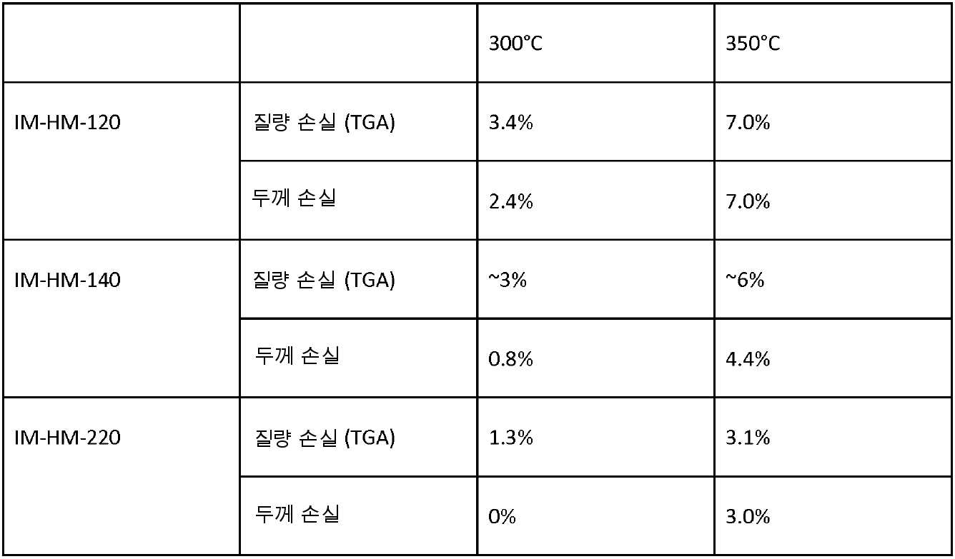
표면 프로파일 측정기(surface Surface profile profilometryprofilometry )() ( DektakDektak ) 및 ) And 엘립소미터(ellipsometry)를The ellipsometry 사용한 막 두께 측정 Measurement of film thickness used
우리의 측정에서 엘립소미터를 사용한 측정은 "Dektak"에 의한 측정보다 상당히 더 두꺼운 막 두께를 제안한다는 점에 유의해야 한다(아래 표 5 참조).It should be noted that in our measurements, measurements using ellipsometry suggest significantly thicker film thicknesses than measurements by "Dektak" (see Table 5, below).
[표 4][Table 4]

모든 막은 1000 rpm에서 스핀되었음.All membranes were spun at 1000 rpm.
IMIM -- HMHM -120 -120 하드마스크에In the hard mask 대한 제조 및 공정 - Manufacturing and Process - 50 g50 g /L의 총 고형분 함량/ L total solids content
- C60 비스-PCBM - C60 Vis-PCBM
- "POLY-OCGEF" 가교제- "POLY-OCGEF" crosslinking agent

C60 비스-PCBM - C60 비스-PCBM (페닐 C60 부티르산 메틸 에스테르)C60 bis-PCBM-C60 bis-PCBM (phenyl C60 butyrate methyl ester)
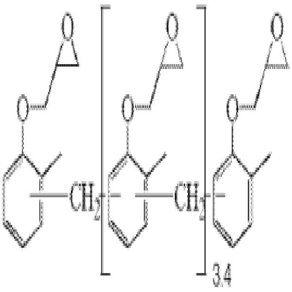
"POLY-OCGEF" - 폴리[(o-크레실 글리시딜 에테르)-코-포름알데하이드, MW = ~1270 "POLY-OCGEF" - poly [(o-cresylglycidyl ether) -co-formaldehyde, MW = ~ 1270
고형분으로부터의 From Solids 하드마스크Hard mask 용액의 제조 Preparation of solution
필요한 경우 공정을 돕기 위해 초음파 교반을 사용하여 50 g/L의 농도로 사이클로헥사논 중의 비스-PCBM 용액을 제조한다. 사이클로헥사논과 양립성이 있는 시린지 필터(syringe filter)(기공 크기 0.02 ㎛) 또는 균등물(50 g/L는 용해도 한계보다 약간 상회함)로 여과한다. If necessary, the bis-PCBM solution in cyclohexanone is prepared at a concentration of 50 g / L using ultrasonic agitation to aid the process. Filter with a syringe filter (pore size 0.02 μm) or equivalent (50 g / L is slightly above the solubility limit) compatible with cyclohexanone.
필요에 따라 공정을 돕기 위해 초음파 교반을 사용하여 50 g/L의 농도로 사이클로헥사논 중의 "POLY-OCGEF" 가교제 용액을 제조한다.A "POLY-OCGEF" crosslinker solution in cyclohexanone is prepared at a concentration of 50 g / L using ultrasonic agitation to assist the process as needed.
하드마스크 용액의 필요한 부피를 제공하기 위해, 각 용액의 동일한 부피를 혼합한다. 혼합을 돕기 위해 초음파 교반을 사용한다.To provide the required volume of the hard mask solution, the same volume of each solution is mixed. Use ultrasonic agitation to aid mixing.
기재 전처리Substrate pretreatment
하드마스크 용액을 적용하기 전에 기재를 깨끗하고 건조하게 유지해야 한다. 표준적인 웨이퍼 세정 및 건조 방법이 적합하게 적용될 수 있다. 일부 경우에, 하드마스크 막 층을 소수성 (즉, HF로 세정된) 표면 상에 스핀 침착하는 것이 유리한 것으로 밝혀졌다.The substrate must be kept clean and dry before applying the hard mask solution. Standard wafer cleaning and drying methods can be suitably applied. In some cases, it has been found advantageous to spin-deposit the hard mask film layer on a hydrophobic (i.e., HF cleaned) surface.
300 ℃에서 스핀 후 베이킹 동안 기저 막의 가스 방출로 인해 하드마스크 막이 손상되는 것을 방지하기 위해 필요한 경우가 아닌 한, 특별한 예비 스핀 탈수 베이킹이 필요하지 않다.A special preliminary spin spin-drying bake is not necessary unless necessary to prevent the hard mask film from being damaged due to gas release of the base film during post-spin bake at 300 占 폚.
주의 - 이 재료는 HMDS 접착 촉진제의 사용과 양립되지 않는다.Caution - This material is not compatible with the use of HMDS adhesion promoters.
하드마스크의Of a hard mask 코팅 coating
막 두께 대 회전 속도 관계를 아래에 나타내었다.The relationship between film thickness and rotational speed is shown below.

표면 프로파일 측정으로부터 얻은, IM-HM-120(이전에는 IM-HM-1이라 불리웠음)에 대한 회전 속도 대 두께The rotational speed versus thickness for IM-HM-120 (formerly called IM-HM-1), obtained from surface profile measurements

엘립소미터로부터 얻은, IM-HM-120(이전에는 IM-HM-1이라 불리웠음)에 대한 회전 속도 대 두께The rotation speed versus thickness for IM-HM-120 (formerly called IM-HM-1), obtained from an ellipsometer
권장되는 코팅 조건은 다음과 같다:The recommended coating conditions are as follows:
a) 정적 분배(static dispense): 전형적으로 0.6 mL가 100 mm 실리콘 웨이퍼를 코팅하는 데 사용된다.a) static dispense: typically 0.6 mL is used to
b) 스프레드 사이클(spread cycle): ~ 167 rpm/초의 상승속도로 500 rpm까지 상승시키고, 5 초 동안 유지한다. b) Spread cycle: raise to 500 rpm at a ramp rate of ~ 167 rpm / sec and hold for 5 s.
c) 회전 사이클(spin cycle): 1 초 미만의 시간 내에 최종 회전 속도까지 상승시키고, 60 초 동안 유지한다. c) spin cycle: raise to the final rotational speed in less than one second and hold for 60 seconds.
베이킹Baking (bake)(bake)
코팅 후, 하드마스크 막을 핫플레이트에서 300 ℃의 온도에서 5 분 동안 베이킹하여, 막이 불용성을 띠도록 한다. After coating, the hard mask film is baked on a hot plate at a temperature of 300 DEG C for 5 minutes to make the film insoluble.
최근의 시도들은 더 짧은 베이킹(2 분 까지 단축될 수 있음)이 막을 불용성으로 만들 것이라고 제안한다.Recent attempts suggest that shorter baking (which can be shortened to two minutes) will render the membrane insoluble.
제거(removal)Removal
제거는 산소 플라즈마 애시(oxygen plasma ash) 또는 반응성 이온 에칭(reactive ion etch)에 의한다.Removal is by oxygen plasma ash or reactive ion etch.
고려된 용매들/이러한 기본적인 Solvents considered / These basic 비스Bis -- PCBMPCBM 하드마스크Hard mask 제형에 대하여 시도되었음 Attempted for formulation
용매는 다음을 포함한다: Solvents include:
사이클로헥사논, 아니솔, 클로로포름, 클로로벤젠Cyclohexanone, anisole, chloroform, chlorobenzene
에칭 기법
실리콘에 대한 선택도
대조군 레지스트
대조군 에칭 속도Etching rate (nm / s)
Etching technique
Selectivity for silicon
Control resist
Control Etch Rate
ICP 혼합 모드 에칭
4.5:1
SAL601
1.24 nm/s0.98 nm / s
ICP mixed mode etch
4.5: 1
SAL601
1.24 nm / s
에칭 기법
실리콘에 대한 선택도
대조군 레지스트
대조군 에칭 속도Etching rate (nm / s)
Etching technique
Selectivity for silicon
Control resist
Control Etch Rate
ICP 혼합 모드 에칭
14.8:1
SAL601
1.34 nm/s0.8 nm / s
ICP mixed mode etch
14.8: 1
SAL601
1.34 nm / s
캐스팅 가능한 두께
(사이클로헥사논)
이용가능한 기타 용매 선택지가 있음Casting solvent
Castable thickness
(Cyclohexanone)
Other solvent options available
130 nm 까지
1.3 ㎛ 까지의 다층이 제조되었음(다른 용매로부터)Cyclohexanone
Up to 130 nm
A multilayer of up to 1.3 μm was prepared (from other solvents)
(경화 후 용출)Solvent compatibility
(Elution after curing)
두께 손실 (에틸 락테이트)
두께 손실 (EEP, 아니솔)
두께 손실 (MCB)
두께 손실 (사이클로헥사논)
두께 손실 (TMAH 25%)Thickness loss (PGME, PGMEA)
Thickness loss (ethyl lactate)
Thickness loss (EEP, Anisole)
Thickness loss (MCB)
Thickness loss (cyclohexanone)
Thickness loss (TMAH 25%)
1분 침지후 용해 없음
1분 침지후 용해 없음
1분 침지후 용해 없음
1분 침지후 용해 없음
1분 침지후 용해 없음No melting after 1 minute immersion
No melting after 1 minute immersion
No melting after 1 minute immersion
No melting after 1 minute immersion
No melting after 1 minute immersion
No melting after 1 minute immersion
질량 손실(TGA)
Thickness loss
Mass loss (TGA)
→ 5분 후 2.4%
두께 손실(%)@350 ℃
→ 5분 후 7.0%
두께 손실(%)@400 ℃
→ 5분 후 14.2%
질량 손실(%)@300 ℃→3.4%
질량 손실(%)@350 ℃→7.0%
질량 손실(%)@400 ℃→14.2%Thickness loss (%) @ 300 ℃
→ 2.4 minutes after 5 minutes
Thickness loss (%) @ 350 ℃
→ After 5 minutes, 7.0%
Thickness loss (%) @ 400 ℃
→ After 5 minutes 14.2%
Mass loss (%) @ 300 占 폚? 3.4%
Mass loss (%) @ 350 占 폚? 7.0%
Mass loss (%) @ 400 ° C → 14.2%
평균 조도
RMS 조도
피크로부터 골짜기 까지의 깊이materials
Average illumination
RMS illuminance
Depth from peak to valley
0.28 nm / 0.28 nm
0.35 nm / 0.36 nm
4.57 nm / 3.12 nmUncoated Silicon / SoC-coated Si
0.28 nm / 0.28 nm
0.35 nm / 0.36 nm
4.57 nm / 3.12 nm
왼쪽:
풀러렌 하드마스크
내로 전사된
30 nm 라인
오른쪽:
실리콘 내로 에칭된
저밀도 20 nm 라인image
left:
Fullerene hard mask
Transferred into
30 nm line
Right side:
Etched into silicon
Low density 20 nm line

특정 고객의 요구에 따라, 50 nm 막 두께에 대한 더 낮은 농도의 제형이 공급되었다.Depending on the needs of the particular customer, a lower concentration of formulation for 50 nm film thickness was supplied.
IMIM -- HMHM -120 -120 하드마스크를Hard mask 위한 공정 - The process - 25 g25 g /L의 총 고형분 함량/ L total solids content
하드마스크의Of a hard mask 코팅 coating
50 nm 두께의 막을 위한 권장되는 코팅 조건은 다음과 같다:The recommended coating conditions for a 50 nm thick film are:
a) 정적 분배: 전형적으로 0.6 mL가 100 mm 실리콘 웨이퍼를 코팅하는 데 사용된다.a) Static dispense: Typically 0.6 mL is used to
b) 스프레드 사이클: ~ 167 rpm/초의 상승속도로 500 rpm까지 상승시키고, 5 초 동안 유지한다.b) Spread cycle: ramp up to 500 rpm at a ramp rate of ~ 167 rpm / sec and hold for 5 s.
c) 회전 사이클: 1 초 미만의 시간 내에 1500 rpm까지 상승시키고, 60 초 동안 유지한다.c) Rotational cycle: raise to 1500 rpm in less than one second and hold for 60 seconds.
베이킹Baking
코팅 후, 하드마스크 막을 핫플레이트에서 300 ℃의 온도에서 5 분 동안 베이킹하여, 막이 불용성을 띠도록 한다. After coating, the hard mask film is baked on a hot plate at a temperature of 300 DEG C for 5 minutes to make the film insoluble.
최근의 시도들은 더 짧은 베이킹(2 분 까지 단축될 수 있음)이 막을 불용성으로 만들 것이라고 제안한다.Recent attempts suggest that shorter baking (which can be shortened to two minutes) will render the membrane insoluble.
제거remove
산소 플라즈마 애시(oxygen plasma ash) 또는 반응성 이온 에칭(reactive ion etch)에 의한 제거가 권장된다.Removal by oxygen plasma ash or reactive ion etch is recommended.
IMIM -- HMHM -140을 위한 제조 및 공정 - 25 내지 -140 < / RTI > 150 g150 g /L의 총 고형분 함량/ L total solids content
- 혼합된 다부가물-PCBM(Mixed Multiadduct-PCBM)(MiMu-PCBM) - Mixed Multiadduct-PCBM (MiMu-PCBM)
- "POLY-OCGEF" 가교제- "POLY-OCGEF" crosslinking agent
고형분으로부터의 From Solids 하드마스크Hard mask 용액의 제조 - Preparation of solution - 50 g50 g /L의 총 고형분에 대한 / L for total solids 실시예Example
필요에 따라 공정을 돕기 위해 초음파 교반을 사용하여 50 g/L의 농도로 사이클로헥사논 중의 혼합된 다부가물-PCBM(MiMu-PCBM) 용액을 제조한다. 사이클로헥사논과 양립되는 기공 크기 0.02 ㎛의 시린지 필터로 또는 균등물로 여과한다.PCM (MiMu-PCBM) solution in cyclohexanone is prepared at a concentration of 50 g / L using ultrasonic agitation to assist the process as needed. It is filtered with a syringe filter of pore size 0.02 탆 compatible with cyclohexanone or with equivalent.
필요에 따라 공정을 돕기 위해 초음파 교반을 사용하여 50 g/L의 농도로 사이클로헥사논 중의 POLY-OCGEF 가교제 용액을 제조한다. A POLY-OCGEF crosslinker solution in cyclohexanone is prepared at a concentration of 50 g / L using ultrasonic agitation to assist the process as needed.
하드마스크 용액의 필요한 부피를 제공하기 위해 각 용액의 동일한 부피를 혼합한다. 혼합을 돕기 위해 초음파 교반을 사용한다. The same volume of each solution is mixed to provide the required volume of the hard mask solution. Use ultrasonic agitation to aid mixing.
기재 전처리Substrate pretreatment
하드마스크 용액을 적용하기 전에 기재를 깨끗하고 건조하게 유지해야 한다. 표준적인 웨이퍼 세정 및 건조 방법이 적합하게 적용될 수 있다. 일부 경우에, 하드마스크 막 층을 소수성 (즉, HF로 세정된) 표면 상에 스핀 코팅하는 것이 유리한 것으로 밝혀졌다.The substrate must be kept clean and dry before applying the hard mask solution. Standard wafer cleaning and drying methods can be suitably applied. In some cases, it has been found advantageous to spin-coat the hard mask film layer on a hydrophobic (i.e., HF cleaned) surface.
300 ℃에서 스핀 후 베이킹 동안 기저 막의 가스 방출로 인해 하드마스크 막이 손상되는 것을 방지하기 위해 필요한 경우가 아닌 한, 특별한 예비 스핀 탈수 베이킹이 필요하지 않다.A special preliminary spin spin-drying bake is not necessary unless necessary to prevent the hard mask film from being damaged due to gas release of the base film during post-spin bake at 300 占 폚.
주의 - 이 재료는 HMDS 접착 촉진제의 사용과 양립되지 않는다.Caution - This material is not compatible with the use of HMDS adhesion promoters.
하드마스크의Of a hard mask 코팅 coating
막 두께 대 회전 속도 관계를 아래에 나타내었다.The relationship between film thickness and rotational speed is shown below.
표준적인 회전 조건은 다음과 같다:The standard rotation conditions are as follows:
a) 정적 분배: 전형적으로 0.6 mL가 100 mm 실리콘 웨이퍼를 코팅하는 데 사용된다.a) Static dispense: Typically 0.6 mL is used to
b) 스프레드 사이클: ~ 167 rpm/초의 상승속도로 500 rpm까지 상승시키고, 5 초 동안 유지한다.b) Spread cycle: ramp up to 500 rpm at a ramp rate of ~ 167 rpm / sec and hold for 5 s.
c) 회전 사이클: 1 초 미만의 시간 내에 최종 회전 속도까지 상승시키고, 60 초 동안 유지한다.c) Rotational cycle: raise to the final rotational speed in less than one second and hold for 60 seconds.
제한된 데이타가 현재 이용가능하다. 그러나, 이 데이타는 150 g/L, 100 g/L, 50 g/L 및 25 g/L의 농도가, 1000 내지 5000 rpm의 속도로, 약 10 nm 내지 약 500 nm를 커버할 수 있다고 시사한다. 이러한 더욱 포괄적인 회전 속도 대 두께 데이터를 생성하는 시험이 진행 중이다. Limited data is currently available. However, this data suggests that concentrations of 150 g / L, 100 g / L, 50 g / L and 25 g / L can cover from about 10 nm to about 500 nm at a rate of 1000 to 5000 rpm . Testing is underway to generate this more comprehensive rotational speed vs. thickness data.
이해되는 바와 같이, 매우 큰 웨이퍼의 경우, 사용가능한 최대 회전 속도는 3000 rpm이다. As will be appreciated, for very large wafers, the maximum rotational speed available is 3000 rpm.
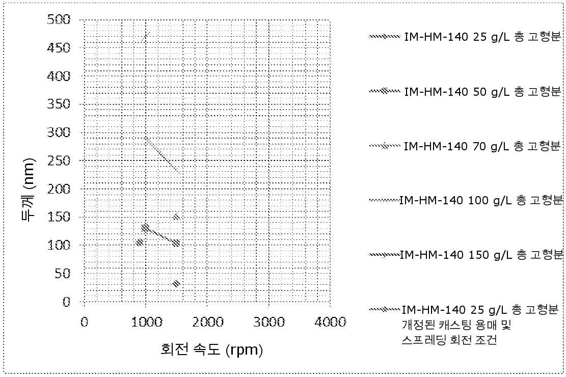
표면 프로파일 측정으로부터 얻은, 현재까지의 회전 속도 대 두께 데이터The rotational speed versus thickness data up to now, obtained from surface profile measurements
개정된 용매는 PGME:사이클로헥사논 1:1이었다. 하드마스크는 다음에 의해 제형화되었다:The modified solvent was PGME: cyclohexanone 1: 1. The hard mask was formulated by:
a) 25 g/L의 농도로 사이클로헥사논 중의 혼합된 다부가물-PCBM(MiMu-PCBM)의 용액을 제조하는 단계;a) preparing a solution of mixed multiparticulates-PCBM (MiMu-PCBM) in cyclohexanone at a concentration of 25 g / L;
b) 25 g/L의 농도로 PGME 중의 POLY-OCGEF 가교제의 용액을 제조하는 단계; 및b) preparing a solution of POLY-OCGEF crosslinker in PGME at a concentration of 25 g / L; And
c) 동일한 부피의 각각의 용액을 혼합하여 필요한 부피의 하드마스크 용액을 제공하는 단계.c) Mixing the same volume of each solution to provide the required volume of the hard mask solution.
PGME 함량을 50 % 이상으로 높이려는 시도는, 베이킹 후 막 품질을 떨어뜨렸다.Attempts to increase the PGME content to more than 50% reduced film quality after baking.
개정된 회전 조건은 다음과 같다:The revised rotation conditions are as follows:
a) 정적 분배: 전형적으로 0.6 mL가 100 mm 실리콘 웨이퍼를 코팅하는 데 사용된다.a) Static dispense: Typically 0.6 mL is used to
b) 연장된 스프레드 사이클: 30 초 동안 500 rpm까지 상승시키고, 5 초 동안 유지한다.b) Extended spread cycle: raise to 500 rpm for 30 seconds and hold for 5 seconds.
c) 회전 사이클: 1 초 미만의 시간 내에 900 rpm의 최종 회전 속도 까지 상승시키고, 60 초 동안 유지한다.c) Rotational cycle: Within a period of less than one second, raise to a final rotational speed of 900 rpm and hold for 60 seconds.
아래 그림은 절반 농도의 풀러렌 유도체(및 POLY-OCGEF 가교제)를 갖는 PGME/사이클로헥사논 캐스팅 용매에서 스핀된, 이러한 혼합 다부가물 PCBM 유도체를 기반으로 한, > 100 nm 두께의 막을 사용한 내식 시험 결과를 보여준다. 명확하게 알 수 있듯이, 새로운 제형의 에칭 내성은 표준 제형과 비교하여 더욱 향상된다.The figure below shows the corrosion test results using a film of> 100 nm thickness based on this mixed multi-adduct PCBM derivative spun in a PGME / cyclohexanone casting solvent with a half concentration of fullerene derivative (and POLY-OCGEF crosslinking agent) Lt; / RTI > As can be clearly seen, the etch resistance of the new formulation is further enhanced compared to the standard formulation.

새로운 저비용 제형에 의한 에칭 내성의 상대적 향상Relative Improvement of Etch Resistance by New Low-Cost Formulations
아래의 SEM 현미경 사진은 새로운 저비용 제형 하드마스크의 > 100 nm 두께 막 내로 27 nm 저밀도 라인과 54 nm 피치의 고밀도 라인(얇은 실험용 레지스트 층의 전자 빔 노출에 의해 패터닝됨)의 성공적인 전사의 초기 이미지를 보여준다. 주의 - 해상도와 선 품질은, IM 하드마스크가 아니라, 사용된 전자 빔 패터닝 툴(tool)에 의해서만 제한된다.The SEM micrographs below show the initial image of a successful transfer of a 27 nm low density line and a high density line of 54 nm pitch (patterned by electron beam exposure of a thin experimental resist layer) into a> 100 nm thick film of a new low cost formulation hard mask Show. Note - Resolution and line quality are limited only by the electron beam patterning tool used, not the IM hard mask.

막 내로 전사된 27 nm 저밀도 라인/ 막 내로 전사된 54 nm 피치 고밀도 라인A 54 nm pitch high density line transferred into a 27 nm low density line / membrane transferred into the film
시도된 다른 개정된 용매 시스템은 하기를 포함한다:Other revised solvent systems attempted include:
사이클로헥사논, 크실렌 및 에틸 락테이트(7:2:1 비율);Cyclohexanone, xylene and ethyl lactate (7: 2: 1 ratio);
사이클로헥사논 및 크실렌(8:2 비율).Cyclohexanone and xylene (8: 2 ratio).
1500 rpm의 회전 속도에 대한 막 두께 The film thickness for a rotation speed of 1500 rpm 대 농도Large concentration
고정된 1500 rpm 최종 회전 속도에서 막 두께 대 풀러렌 농도(최종 제형 내) 사이의 관계를 아래에 나타내었다.The relationship between film thickness versus fullerene concentration (in the final formulation) at a fixed 1500 rpm final rotational speed is shown below.

1500 rpm 스핀 최종 회전 속도에 대한 최종 제형의 막 두께 대 풀러렌 농도(표면 프로파일 측정으로부터)1500 rpm Final film thickness versus fullerene concentration (from surface profile measurement)
표준적인 스핀 코팅 조건은 다음과 같다:Standard spin coating conditions are as follows:
a) 정적 분배: 전형적으로 0.6 mL가 100 mm 실리콘 웨이퍼를 코팅하는 데 사용된다.a) Static dispense: Typically 0.6 mL is used to
b) 스프레드 사이클: ~167 rpm/초의 상승속도로 500 rpm까지 상승시키고, 5 초 동안 유지한다.b) Spread cycle: ramp up to 500 rpm at a ramp rate of ~ 167 rpm / sec and hold for 5 s.
c) 회전 사이클: 1 초 미만의 시간 내에 최종 회전 속도 까지 상승시키고, 60 초 동안 유지한다.c) Rotational cycle: raise to the final rotational speed in less than one second and hold for 60 seconds.
개정된 스핀 코팅 조건은 다음과 같다:The modified spin coating conditions are as follows:
a) 정적 분배: 전형적으로 0.6 mL가 100 mm 실리콘 웨이퍼를 코팅하는 데 사용된다.a) Static dispense: Typically 0.6 mL is used to
b) 연장된 스프레드 사이클: 30 초 동안 500 rpm까지 상승시키고, 5 초 동안 유지한다.b) Extended spread cycle: raise to 500 rpm for 30 seconds and hold for 5 seconds.
c) 회전 사이클: 1 초 미만의 시간 내에 최종 회전 속도 까지 상승시키고, 60 초 동안 유지한다.c) Rotational cycle: raise to the final rotational speed in less than one second and hold for 60 seconds.
IMIM -- HMHM -220 -220 하드마스크를Hard mask 위한 준비 및 공정 Preparation and process
- C60 비스-PCBA - C 60 bis -PCBA
- 플루오렌 디아닐린 가교제- fluorenedianiline crosslinking agent

C60 PCBA - PCBM의 모노-카르복실산 형태C60 PCBA - mono-carboxylic acid form of PCBM
플루오렌 디아닐린 가교제 - 4,4'-(9-플루오레닐리덴)디아닐린Fluorene dianiline crosslinking agent - 4,4 '- (9-fluorenylidene) dianiline
이 제형은 개선된 열 안정성 및 증가된 탄소 함량을 제공했다:This formulation provided improved thermal stability and increased carbon content:
플루오렌 디아닐린 가교제를 갖는 C60 비스-PCBA에 대하여 87.6% 탄소;87.6% carbon for C60 bis-PCBA with fluorene dianiline crosslinker;
플루오렌 디아닐린 가교제를 갖는 혼합된 다부가물-PCBA에 대하여 87.5% 탄소.87.5% carbon for mixed multifunctional-PCBA with fluorene dianiline crosslinker.
고형분으로부터 From solid content 하드마스크Hard mask 용액의 제조 Preparation of solution
필요한 경우 공정을 돕기 위해 초음파 교반을 사용하여 50 g/L의 농도로 사이클로헥사논 중의 비스-PCBA 용액을 제조한다. 사이클로헥사논과 양립되는 시린지 필터(syringe filter)(기공 크기 0.02 ㎛) 또는 균등물(50 g/L는 용해도 한계보다 약간 상회함)로 여과한다. If necessary, the bis-PCBA solution in cyclohexanone is prepared at a concentration of 50 g / L using ultrasonic agitation to aid the process. Filter with a syringe filter (pore size 0.02 μm) compatible with cyclohexanone or equivalent (slightly above 50 g / L solubility limit).
필요에 따라 공정을 돕기 위해 초음파 교반을 사용하여 50 g/L의 농도로 사이클로헥사논 중의 플루오렌 디아닐린 가교제 용액을 제조한다.A solution of fluorenedianiline crosslinker in cyclohexanone is prepared at a concentration of 50 g / L using ultrasonic agitation to assist the process as needed.
하드마스크 용액의 필요한 부피를 제공하기 위해, 각 용액의 동일한 부피를 혼합한다. 혼합을 돕기 위해 초음파 교반을 사용한다.To provide the required volume of the hard mask solution, the same volume of each solution is mixed. Use ultrasonic agitation to aid mixing.
기재 전처리Substrate pretreatment
하드마스크 용액을 적용하기 전에 기재를 깨끗하고 건조하게 유지해야 한다. 표준적인 웨이퍼 세정 및 건조 방법이 적합하게 적용될 수 있다. 일부 경우에, 하드마스크 막 층을 소수성 (즉, HF로 세정된) 표면 상에 스핀 코팅하는 것이 유리한 것으로 밝혀졌다.The substrate must be kept clean and dry before applying the hard mask solution. Standard wafer cleaning and drying methods can be suitably applied. In some cases, it has been found advantageous to spin-coat the hard mask film layer on a hydrophobic (i.e., HF cleaned) surface.
300 ℃에서 스핀-후 베이킹 동안 기저 막의 가스 방출로 인해 하드마스크 막이 손상되는 것을 방지하기 위해 필요한 경우가 아닌 한, 특별한 예비 스핀 탈수 베이킹이 필요하지 않다.No special pre-spin spin-drying bake is required unless necessary to prevent damage to the hard mask film due to gas release of the base film during post-spin bake at 300 ° C.
주의 - 이 재료는 HMDS 접착 촉진제의 사용과 양립되지 않는다.Caution - This material is not compatible with the use of HMDS adhesion promoters.
하드마스크의Of a hard mask 코팅 및 Coating and 가교결합Crosslinking 베이킹Baking 요건 Requirements
좋은 품질의 막이 PCBA/디아닐린 하드마스크 제형에서 스핀되었고, 유망한 열 안정성과 에칭 데이터가 2 페이지와 3 페이지의 표에 제시되었지만(5 분 동안 250 ℃의 가교 베이킹으로 제공된 ~ 120 nm 두께의 막으로부터 얻음), 다음과 같은 측면에서 용액의 성능이 시간에 따라(5 ℃에서 보관됨) 변화하는 것으로 나타났으므로 상기 재료는 추가 연구가 필요하다:Although a good quality film was spun in a PCBA / dianiline hardmask formulation and the promising thermal stability and etch data are shown in the tables on
회전 속도 두께 관계가 변화한다(주어진 세트의 조건으로 스핀된 막의 두께가 증가한다); 및The rotational speed thickness relationship changes (the thickness of the film spun under a given set of conditions increases); And
재료를 완전히 가교시키는데 필요한 베이킹 량이 감소한다(즉, 감소된 가교 베이킹 온도 또는 감소된 시간).The amount of baking needed to completely crosslink the material is reduced (i. E., Reduced cross-linking baking temperature or reduced time).
상기 재료가 용액 중에서 가교결합되는 것으로 시사된다.It is suggested that the material is cross-linked in solution.
CL06-10 가교제: 폴리[(o-크레실 글리시딜 에테르)-코-포름알데히드CL06-10 Crosslinking agent: poly [(o-cresylglycidyl ether) -co-formaldehyde
EEP: 에틸 3-에톡시프로피오네이트EEP: ethyl 3-ethoxypropionate
플루오렌 디아닐린 가교제: 4,4' (9 플루오레닐리덴)디아닐린Fluorene dianiline Crosslinking agent: 4,4 '(9-fluorenylidene) dianiline
MiMu-PCBM: 혼합된 다부가물 PCBM(Mixed multi-adduct PCBM)MiMu-PCBM: Mixed multi-adduct PCBM (PCBM)
POLY-OCGEF: 폴리[(o-크레실 글리시딜 에테르)-코-포름알데히드POLY-OCGEF: Poly [(o-cresylglycidyl ether) -co-formaldehyde
Claims (14)
상기 풀러렌 유도체는 하기 화학식 (I)로 표시되고:
<화학식 (I)>
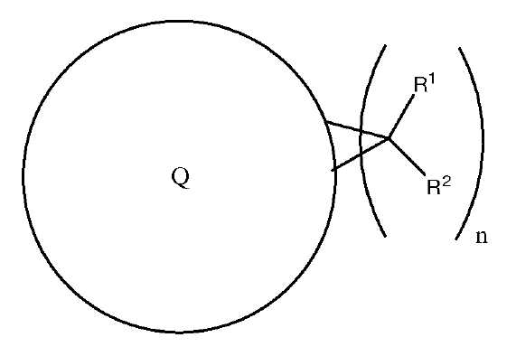
여기서, n은 1 내지 6의 정수이고, 풀러렌 내 탄소원자 개수인 Q는 60, 70, 76, 78, 80, 82 또는 84이고, R1은 에스테르, 알코올, 페놀, 아민, 아미드, 이미드 또는 카르복실산을 포함하는 제1 치환기를 나타내고, R2는 수소, 할로겐, C6-C20 아릴기, C1-C20 알킬기, 에스테르, 알코올, 페놀, 아민, 아미드, 이미드 또는 카르복실산을 포함하는 제2 치환기를 나타내며,
상기 가교제는 둘 이상의 열적 또는 촉매적 반응성 기를 포함하는,
조성물.A composition for forming a spin-on hard mask comprising a fullerene derivative and a cross-linking agent,
Wherein said fullerene derivative is represented by the following formula (I)
≪ Formula (I) >
Where n is an integer from 1 to 6 and Q, the number of carbon atoms in the fullerene, is 60, 70, 76, 78, 80, 82 or 84 and R 1 is an ester, alcohol, phenol, amine, amide, R 2 represents a hydrogen atom, a halogen, a C 6 -C 20 aryl group, a C 1 -C 20 alkyl group, an ester, an alcohol, a phenol, an amine, an amide, an imide or a carboxylic acid , ≪ / RTI >
Wherein the crosslinking agent comprises two or more thermally or catalytically reactive groups.
Composition.
b) 코팅을 기재 상에 형성하는 단계; 및
c) 상기 기재 및 상기 코팅을, 상기 코팅을 가교결합시키기에 충분한 온도에서, 가열하는 단계;를 포함하는 스핀-온 하드마스크 형성 방법.a) providing a composition according to any one of claims 1 to 13;
b) forming a coating on the substrate; And
c) heating the substrate and the coating at a temperature sufficient to crosslink the coating.
Applications Claiming Priority (3)
| Application Number | Priority Date | Filing Date | Title |
|---|---|---|---|
| US201462061294P | 2014-10-08 | 2014-10-08 | |
| US62/061,294 | 2014-10-08 | ||
| PCT/US2015/064089 WO2016058008A2 (en) | 2014-10-08 | 2015-12-04 | Spin on hard-mask material |
Publications (2)
| Publication Number | Publication Date |
|---|---|
| KR20170105480A true KR20170105480A (en) | 2017-09-19 |
| KR102514100B1 KR102514100B1 (en) | 2023-03-24 |
Family
ID=55653963
Family Applications (1)
| Application Number | Title | Priority Date | Filing Date |
|---|---|---|---|
| KR1020177012083A KR102514100B1 (en) | 2014-10-08 | 2015-12-04 | Spin on Hard-mask Material |
Country Status (5)
| Country | Link |
|---|---|
| US (1) | US10290500B2 (en) |
| JP (1) | JP6967967B2 (en) |
| KR (1) | KR102514100B1 (en) |
| CN (1) | CN107207259A (en) |
| WO (1) | WO2016058008A2 (en) |
Cited By (3)
| Publication number | Priority date | Publication date | Assignee | Title |
|---|---|---|---|---|
| KR20200104564A (en) * | 2019-02-27 | 2020-09-04 | 동우 화인켐 주식회사 | Composition for hard mask |
| KR20200125662A (en) * | 2018-02-25 | 2020-11-04 | 알렉스 필립 그레이엄 로빈손 | Hard mask composition |
| KR20220021315A (en) * | 2020-08-13 | 2022-02-22 | 삼성에스디아이 주식회사 | Hardmask composition and method of forming patterns |
Families Citing this family (3)
| Publication number | Priority date | Publication date | Assignee | Title |
|---|---|---|---|---|
| KR102675775B1 (en) * | 2016-12-27 | 2024-06-18 | 삼성전자주식회사 | Hardmask composition, method of forming patterning using the hardmask composition, and hardmask formed from the hardmask composition |
| US10475991B2 (en) | 2018-02-22 | 2019-11-12 | Taiwan Semiconductor Manufacturing Company, Ltd. | Fabrication of large height top metal electrode for sub-60nm magnetoresistive random access memory (MRAM) devices |
| CN109461817B (en) * | 2018-09-20 | 2020-05-12 | 中国科学院半导体研究所 | Method for manufacturing metal micro-nano structure on surface of halide perovskite film |
Citations (4)
| Publication number | Priority date | Publication date | Assignee | Title |
|---|---|---|---|---|
| JP2004264710A (en) * | 2003-03-04 | 2004-09-24 | Jsr Corp | Antireflection film forming composition and antireflection film |
| JP2004279694A (en) * | 2003-03-14 | 2004-10-07 | Nippon Telegr & Teleph Corp <Ntt> | Resist composition and its hardening method |
| KR20110091479A (en) * | 2010-02-05 | 2011-08-11 | 신에쓰 가가꾸 고교 가부시끼가이샤 | Resist underlayer film composition, process for forming resist underlayer film, patterning process and fullerene derivative |
| KR20150028221A (en) * | 2012-02-10 | 2015-03-13 | 더 유니버시티 오브 버밍험 | Spin on hard-mask material |
Family Cites Families (11)
| Publication number | Priority date | Publication date | Assignee | Title |
|---|---|---|---|---|
| JPH07306531A (en) * | 1994-05-11 | 1995-11-21 | Japan Synthetic Rubber Co Ltd | Radiation sensitive resin composition |
| US7264617B2 (en) * | 2000-02-29 | 2007-09-04 | Alex Freeman | Integrally manufactured micro-electrofluidic cables |
| JPWO2003079475A1 (en) * | 2002-03-20 | 2005-07-21 | 株式会社三昌化工 | FUEL CELL SEPARATOR, MANUFACTURING METHOD THEREOF, AND FUEL CELL USING THE FUEL CELL SEPARATOR |
| JP4496432B2 (en) * | 2005-02-18 | 2010-07-07 | 信越化学工業株式会社 | Photoresist underlayer film forming material and pattern forming method |
| CN101641644B (en) * | 2007-04-06 | 2012-07-04 | 日产化学工业株式会社 | Composition for forming under-resist film |
| US8592134B2 (en) * | 2007-12-07 | 2013-11-26 | Mitsubishi Gas Chemical Company, Inc. | Composition for forming base film for lithography and method for forming multilayer resist pattern |
| GB0920231D0 (en) * | 2009-11-18 | 2010-01-06 | Univ Birmingham | Photoresist composition |
| JP5757286B2 (en) * | 2010-03-01 | 2015-07-29 | 日産化学工業株式会社 | Resist underlayer film forming composition containing fullerene derivative |
| US9383646B2 (en) * | 2014-02-24 | 2016-07-05 | Irresistible Materials Ltd | Two-step photoresist compositions and methods |
| US9255172B1 (en) * | 2014-08-05 | 2016-02-09 | International Business Machines Corporation | High-performance, filler-reinforced, recyclable composite materials |
| JP6628052B2 (en) * | 2015-03-11 | 2020-01-08 | 日産化学株式会社 | Method of forming resist underlayer film |
-
2015
- 2015-12-04 JP JP2017519309A patent/JP6967967B2/en active Active
- 2015-12-04 CN CN201580054194.6A patent/CN107207259A/en active Pending
- 2015-12-04 KR KR1020177012083A patent/KR102514100B1/en active IP Right Grant
- 2015-12-04 WO PCT/US2015/064089 patent/WO2016058008A2/en active Application Filing
- 2015-12-04 US US15/511,416 patent/US10290500B2/en active Active
Patent Citations (4)
| Publication number | Priority date | Publication date | Assignee | Title |
|---|---|---|---|---|
| JP2004264710A (en) * | 2003-03-04 | 2004-09-24 | Jsr Corp | Antireflection film forming composition and antireflection film |
| JP2004279694A (en) * | 2003-03-14 | 2004-10-07 | Nippon Telegr & Teleph Corp <Ntt> | Resist composition and its hardening method |
| KR20110091479A (en) * | 2010-02-05 | 2011-08-11 | 신에쓰 가가꾸 고교 가부시끼가이샤 | Resist underlayer film composition, process for forming resist underlayer film, patterning process and fullerene derivative |
| KR20150028221A (en) * | 2012-02-10 | 2015-03-13 | 더 유니버시티 오브 버밍험 | Spin on hard-mask material |
Cited By (3)
| Publication number | Priority date | Publication date | Assignee | Title |
|---|---|---|---|---|
| KR20200125662A (en) * | 2018-02-25 | 2020-11-04 | 알렉스 필립 그레이엄 로빈손 | Hard mask composition |
| KR20200104564A (en) * | 2019-02-27 | 2020-09-04 | 동우 화인켐 주식회사 | Composition for hard mask |
| KR20220021315A (en) * | 2020-08-13 | 2022-02-22 | 삼성에스디아이 주식회사 | Hardmask composition and method of forming patterns |
Also Published As
| Publication number | Publication date |
|---|---|
| WO2016058008A3 (en) | 2016-05-26 |
| JP2017533464A (en) | 2017-11-09 |
| CN107207259A (en) | 2017-09-26 |
| KR102514100B1 (en) | 2023-03-24 |
| US10290500B2 (en) | 2019-05-14 |
| US20170278703A1 (en) | 2017-09-28 |
| JP6967967B2 (en) | 2021-11-17 |
| WO2016058008A2 (en) | 2016-04-14 |
Similar Documents
| Publication | Publication Date | Title |
|---|---|---|
| JP6284887B2 (en) | Spin-on hard mask material | |
| KR102514100B1 (en) | Spin on Hard-mask Material | |
| TW200905401A (en) | Resist underlayer coating forming composition | |
| KR20160107102A (en) | Composition for forming resist lower layer film, resist lower layer film, and process for producing patterned substrate | |
| TW201838959A (en) | Novel compound, semiconductor material, and methods for manufacturing coating and semiconductor using the same | |
| US7514200B2 (en) | Hard mask composition for lithography process | |
| JP2024061788A (en) | Coated underlying layer for overcoated photoresist | |
| JP7349887B2 (en) | Composition for forming hard mask and method for producing electronic components | |
| KR102638159B1 (en) | Hard mask composition | |
| JP7523256B2 (en) | Composition for forming hard mask and method for producing electronic component | |
| TWI759303B (en) | Hard-mask composition | |
| TWI797266B (en) | Hard mask composition | |
| KR102648023B1 (en) | Coating compositions and methods of forming electronic devices | |
| US11746255B2 (en) | Hard-mask composition | |
| KR102542440B1 (en) | Composition for hard mask | |
| JP2018091942A (en) | Flattened film formation composition, flattened film prepared therewith, and method for producing device using the same | |
| KR20170104270A (en) | Composition for hard mask | |
| KR20170104272A (en) | Composition for hard mask |
Legal Events
| Date | Code | Title | Description |
|---|---|---|---|
| A201 | Request for examination | ||
| E902 | Notification of reason for refusal | ||
| E701 | Decision to grant or registration of patent right | ||
| GRNT | Written decision to grant |