KR20170102477A - Thermoelectric conversion device and electricity storage system - Google Patents
Thermoelectric conversion device and electricity storage system Download PDFInfo
- Publication number
- KR20170102477A KR20170102477A KR1020177018289A KR20177018289A KR20170102477A KR 20170102477 A KR20170102477 A KR 20170102477A KR 1020177018289 A KR1020177018289 A KR 1020177018289A KR 20177018289 A KR20177018289 A KR 20177018289A KR 20170102477 A KR20170102477 A KR 20170102477A
- Authority
- KR
- South Korea
- Prior art keywords
- thermoelectric conversion
- conversion device
- layer
- electrode layer
- thermoelectric
- Prior art date
Links
Images


Classifications
-
- H—ELECTRICITY
- H10—SEMICONDUCTOR DEVICES; ELECTRIC SOLID-STATE DEVICES NOT OTHERWISE PROVIDED FOR
- H10N—ELECTRIC SOLID-STATE DEVICES NOT OTHERWISE PROVIDED FOR
- H10N10/00—Thermoelectric devices comprising a junction of dissimilar materials, i.e. devices exhibiting Seebeck or Peltier effects
- H10N10/10—Thermoelectric devices comprising a junction of dissimilar materials, i.e. devices exhibiting Seebeck or Peltier effects operating with only the Peltier or Seebeck effects
- H10N10/17—Thermoelectric devices comprising a junction of dissimilar materials, i.e. devices exhibiting Seebeck or Peltier effects operating with only the Peltier or Seebeck effects characterised by the structure or configuration of the cell or thermocouple forming the device
-
- H01L35/32—
-
- C—CHEMISTRY; METALLURGY
- C23—COATING METALLIC MATERIAL; COATING MATERIAL WITH METALLIC MATERIAL; CHEMICAL SURFACE TREATMENT; DIFFUSION TREATMENT OF METALLIC MATERIAL; COATING BY VACUUM EVAPORATION, BY SPUTTERING, BY ION IMPLANTATION OR BY CHEMICAL VAPOUR DEPOSITION, IN GENERAL; INHIBITING CORROSION OF METALLIC MATERIAL OR INCRUSTATION IN GENERAL
- C23C—COATING METALLIC MATERIAL; COATING MATERIAL WITH METALLIC MATERIAL; SURFACE TREATMENT OF METALLIC MATERIAL BY DIFFUSION INTO THE SURFACE, BY CHEMICAL CONVERSION OR SUBSTITUTION; COATING BY VACUUM EVAPORATION, BY SPUTTERING, BY ION IMPLANTATION OR BY CHEMICAL VAPOUR DEPOSITION, IN GENERAL
- C23C14/00—Coating by vacuum evaporation, by sputtering or by ion implantation of the coating forming material
- C23C14/06—Coating by vacuum evaporation, by sputtering or by ion implantation of the coating forming material characterised by the coating material
- C23C14/08—Oxides
-
- H01L35/22—
-
- H01L35/24—
-
- H01L51/00—
-
- H—ELECTRICITY
- H02—GENERATION; CONVERSION OR DISTRIBUTION OF ELECTRIC POWER
- H02N—ELECTRIC MACHINES NOT OTHERWISE PROVIDED FOR
- H02N11/00—Generators or motors not provided for elsewhere; Alleged perpetua mobilia obtained by electric or magnetic means
-
- H—ELECTRICITY
- H10—SEMICONDUCTOR DEVICES; ELECTRIC SOLID-STATE DEVICES NOT OTHERWISE PROVIDED FOR
- H10K—ORGANIC ELECTRIC SOLID-STATE DEVICES
- H10K99/00—Subject matter not provided for in other groups of this subclass
-
- H—ELECTRICITY
- H10—SEMICONDUCTOR DEVICES; ELECTRIC SOLID-STATE DEVICES NOT OTHERWISE PROVIDED FOR
- H10N—ELECTRIC SOLID-STATE DEVICES NOT OTHERWISE PROVIDED FOR
- H10N10/00—Thermoelectric devices comprising a junction of dissimilar materials, i.e. devices exhibiting Seebeck or Peltier effects
- H10N10/80—Constructional details
- H10N10/85—Thermoelectric active materials
- H10N10/851—Thermoelectric active materials comprising inorganic compositions
- H10N10/855—Thermoelectric active materials comprising inorganic compositions comprising compounds containing boron, carbon, oxygen or nitrogen
-
- H—ELECTRICITY
- H10—SEMICONDUCTOR DEVICES; ELECTRIC SOLID-STATE DEVICES NOT OTHERWISE PROVIDED FOR
- H10N—ELECTRIC SOLID-STATE DEVICES NOT OTHERWISE PROVIDED FOR
- H10N10/00—Thermoelectric devices comprising a junction of dissimilar materials, i.e. devices exhibiting Seebeck or Peltier effects
- H10N10/80—Constructional details
- H10N10/85—Thermoelectric active materials
- H10N10/856—Thermoelectric active materials comprising organic compositions
Abstract
광 투과성을 구비하고, 열 에너지로부터 전기 에너지를 회생하는 것이 가능한 열전 변환 장치를 제공하는 것이고, 열전 재료로 형성된 열전 변환층과, 해당 열전 변환층에 접속된 전극층을 구비하는 열전 변환 장치이며, 해당 열전 변환층 및 해당 전극층 중 적어도 해당 열전 변환층이 광 투과성을 갖는 열전 변환 장치이다.A thermoelectric conversion device having optical transparency and capable of regenerating electric energy from thermal energy, the thermoelectric conversion device comprising a thermoelectric conversion layer formed of a thermoelectric material and an electrode layer connected to the thermoelectric conversion layer, Wherein at least the thermoelectric conversion layer among the thermoelectric conversion layer and the electrode layer has optical transparency.
Description
본 발명은 기재, 열전 변환층 및 전극층 중 적어도 기재 및 열전 변환층이 광 투과성을 갖는 열전 변환 장치 및 축전 시스템에 관한 것이다.The present invention relates to a thermoelectric conversion device and a power storage system in which at least a substrate and a thermoelectric conversion layer among a substrate, a thermoelectric conversion layer and an electrode layer have light transmittance.
열전 재료는, 재료의 양단에 온도차를 부여함으로써 전위차가 발생하는 특성을 갖는다. 또한, 반대로, 열전 재료에 전위차를 부여함으로써, 온도차가 발생하여, 열 에너지의 방출 또는 흡수가 일어나, 주위의 온도를 상승 또는 하강시키는 특성을 갖는다. 열전 재료의 이러한 특성을 활용한 일례로서, 투명성을 갖는 열전 재료를 사용한 열전 변환 디바이스를 창 유리 등에 접착한 상태에서 통전함으로써, 냉각 장치로서 기능시키는 기술이 개시되어 있다(특허문헌 1 참조).The thermoelectric material has a characteristic in which a potential difference is generated by imparting a temperature difference to both ends of the material. On the contrary, by imparting a potential difference to the thermoelectric material, a temperature difference is generated to cause release or absorption of heat energy, and the characteristic has a property of raising or lowering the ambient temperature. As an example utilizing this characteristic of the thermoelectric material, there is disclosed a technique of functioning as a cooling device by energizing a thermoelectric conversion device using a thermoelectric material having transparency in a state of being adhered to a window glass or the like (see Patent Document 1).
근년, 환경에 대한 배려나 에너지 절약에 대한 관심의 고조로부터, 열전 재료의 상술한 특성을 살려서, 예를 들어 상술한 특허문헌 1의 기술과는 반대의 열전 재료의 특성을 이용하여, 항상적으로 온도차가 발생하는 장소에 열전 변환 디바이스를 배치함으로써, 열 에너지로부터 전기 에너지를 회생하는 기술이 검토되고 있다.In recent years, by taking advantage of the above-mentioned characteristics of the thermoelectric material from the consideration of the environment and the interest in energy saving, it is possible to utilize the characteristics of the thermoelectric material contrary to the technology of the above-mentioned
본 발명은, 열전 변환 디바이스의 한층 더한 응용으로서, 광 투과성을 구비하고, 열 에너지로부터 전기 에너지를 회생하는 것이 가능한 열전 변환 장치 및 축전 시스템을 제공하는 것을 과제로 한다.A further object of the present invention is to provide a thermoelectric conversion device and a power storage system which have optical transparency and can regenerate electric energy from thermal energy as a further application of the thermoelectric conversion device.
본 발명은 이하의 (1) 내지 (9)를 제공하는 것이다.The present invention provides the following (1) to (9).
(1) 열전 재료로 형성된 열전 변환층과, 해당 열전 변환층에 접속된 전극층을 구비하는 열전 변환 장치이며, 해당 열전 변환층 및 해당 전극층 중 적어도 해당 열전 변환층이 광 투과성을 갖는 열전 변환 장치.(1) A thermoelectric conversion device comprising a thermoelectric conversion layer formed of a thermoelectric material and an electrode layer connected to the thermoelectric conversion layer, wherein at least the thermoelectric conversion layer of the thermoelectric conversion layer and the electrode layer has light transmittance.
(2) 상기 열전 변환층 및 상기 전극층 중 적어도 상기 열전 변환층이 해당 열전 변환층의 평면에 교차하는 방향에 있어서, 분광 광도계를 사용하여 측정되는 550nm의 가시광 투과율이 60% 이상인 상기 (1)에 기재된 열전 변환 장치.(2) In the above (1), in which at least the thermoelectric conversion layer of the thermoelectric conversion layer and the electrode layer cross the plane of the thermoelectric conversion layer and the visible light transmittance at 550 nm measured using a spectrophotometer is 60% A thermoelectric conversion device as set forth in
(3) 상기 열전 변환층과 상기 전극층이 표면에 배치된 기재를 갖고, 해당 기재가 광 투과성을 갖는 무기계 재료 또는 광 투과성을 갖는 유기계 재료인 상기 (1) 또는 (2)에 기재된 열전 변환 장치.(3) The thermoelectric conversion device according to the above (1) or (2), wherein the thermoelectric conversion layer and the electrode layer have a base material on the surface and the base material is an inorganic material having light transmission property or an organic material having light transmission property.
(4) 상기 열전 재료가 n형 열전 재료인 상기 (1) 내지 (3) 중 어느 한 항에 기재된 열전 변환 장치.(4) The thermoelectric conversion device according to any one of (1) to (3), wherein the thermoelectric material is an n-type thermoelectric material.
(5) 상기 열전 재료가 p형 열전 재료인 상기 (1) 내지 (3) 중 어느 한 항에 기재된 열전 변환 장치.(5) The thermoelectric conversion device according to any one of (1) to (3), wherein the thermoelectric material is a p-type thermoelectric material.
(6) 상기 열전 변환층이 n형 열전 재료로 형성된 n형 열전 변환층 및 p형 열전 재료로 형성된 p형 열전 변환층을 갖고, 해당 n형 열전 변환층 및 해당 p형 열전 변환층이 상기 전극층에 의해 접속되어 있는 상기 (1) 내지 (5) 중 어느 한 항에 기재된 열전 변환 장치.(6) The thermoelectric conversion element according to any one of (6) to (7), wherein the thermoelectric conversion layer has an n-type thermoelectric conversion layer formed of an n-type thermoelectric material and a p-type thermoelectric conversion layer formed of a p- The thermoelectric conversion device according to any one of (1) to (5), wherein the thermoelectric conversion device is connected to the thermoelectric conversion device.
(7) 상기 열전 변환 장치의 평면적(平面積)에 대한, 상기 전극층이 형성된 영역을 제외한 영역의 면적의 비율이 1% 이상 99% 이하인 상기 (1) 내지 (6) 중 어느 한 항에 기재된 열전 변환 장치.(7) The thermoelectric conversion element according to any one of (1) to (6) above, wherein the ratio of the area of the area excluding the region where the electrode layer is formed to the flat area of the thermoelectric conversion device is not less than 1% and not more than 99% Conversion device.
(8) 상기 전극층이 광 투과성을 갖는 상기 (1) 내지 (7) 중 어느 한 항에 기재된 열전 변환 장치.(8) The thermoelectric conversion device according to any one of (1) to (7), wherein the electrode layer has light transmittance.
(9) 상기 (1) 내지 (8) 중 어느 한 항에 기재된 열전 변환 장치와, 전기를 축전하는 축전 장치를 구비하고, 해당 열전 변환 장치에 있어서의 상기 전극층이 해당 축전 장치에 전기적으로 접속되어 이루어지는 축전 시스템.(9) A thermoelectric conversion device as described in any one of (1) to (8) above, and a power storage device for storing electricity, wherein the electrode layer of the thermoelectric conversion device is electrically connected to the power storage device The power storage system.
본 발명에 따르면, 광 투과성을 구비하고, 열 에너지로부터 전기 에너지를 회생하는 것이 가능한 열전 변환 장치 및 축전 시스템을 제공할 수 있다.According to the present invention, it is possible to provide a thermoelectric conversion device and a power storage system that have optical transparency and can regenerate electric energy from thermal energy.
도 1은, 본 발명의 실시 형태에 따른 열전 변환 장치(1)의 주면(主面)에 수직 방향으로부터 본 평면도이다.
도 2는, 도 1에 도시하는 F1-F1선에 있어서의 단면도이다.
도 3은, 본 발명의 실시 형태에 따른 열전 변환 장치(2)의 주면에 수직 방향으로부터 본 평면도이다.
도 4는, 도 3에 도시하는 F3-F3선에 있어서의 단면도이다.
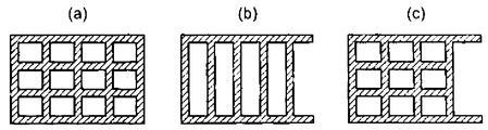
도 5는, 본 실시 형태에 따른 열전 변환 장치의 전극층의 미세 구조의 일례를 설명하는 모식도이다.
도 6은, 본 실시 형태에 따른 열전 변환 장치의 전극층의 미세 구조의 일례를 설명하는 모식도이다.1 is a plan view of a
Fig. 2 is a cross-sectional view taken along line F1-F1 shown in Fig.
3 is a plan view of the
4 is a cross-sectional view taken along the line F3-F3 shown in Fig.
5 is a schematic view for explaining an example of the microstructure of the electrode layer of the thermoelectric conversion device according to the present embodiment.
6 is a schematic view for explaining an example of the microstructure of the electrode layer of the thermoelectric conversion device according to the present embodiment.
[열전 변환 장치][Thermoelectric conversion device]
본 발명의 실시 형태에 따른 열전 변환 장치는, 열전 재료로 형성된 열전 변환층과, 해당 열전 변환층에 접속된 전극층을 구비하는 열전 변환 장치이며, 해당 열전 변환층 및 해당 전극층 중 적어도 해당 열전 변환층이 광 투과성을 갖는다.A thermoelectric conversion device according to an embodiment of the present invention is a thermoelectric conversion device comprising a thermoelectric conversion layer formed of a thermoelectric material and an electrode layer connected to the thermoelectric conversion layer, wherein at least the thermoelectric conversion layer And has light transmittance.
[열전 변환 장치의 구성][Configuration of thermoelectric conversion device]
본 발명의 실시 형태에 따른 열전 변환 장치(1, 2)에 대해서, 도면을 사용하여 상세하게 설명한다. 도 1은, 시트 형상으로 형성된 열전 변환 장치(1)의 주면에 수직 방향으로부터 본 평면도이고, 도 2는, 도 1에 도시하는 F1-F1선에 있어서의 단면도이다.The
열전 변환 장치(1)는, 기재(11)와, 해당 기재(11)의 표면에 배치되어 있고 열전 재료로 형성된 열전 변환층(12)(p형 반도체층) 및 열전 변환층(13)(n형 열전 변환층)과, 해당 열전 변환층(12, 13)에 접속된 전극층(14)을 구비한 pn 접합형의 구조를 갖는다. 열전 변환 장치(1)는, 기재(11), 열전 변환층(12, 13) 및 전극층(14) 중 적어도 기재(11) 및 열전 변환층(12, 13)이 광 투과성을 갖는다. 각 구성 요건은, 후단에서 상세하게 설명한다.The
도 3 및 도 4에 도시하는 열전 변환 장치(2)는, 열전 변환 장치(1)와는 열전 변환층의 구성이 상이하다. p형 열전 변환층 및 n형 열전 변환층으로부터 선택되는 1종류의 열전 변환층을 사용한, 소위 싱글 레그 타입의 구조를 갖는다. 도 3은, 시트 형상으로 형성된 열전 변환 장치(2)의 주면에 수직 방향으로부터 본 평면도이고, 도 4는, 도 3에 도시하는 F3-F3선에 있어서의 단면도이다.The
열전 변환 장치(2)는, 기재(21)와, 열전 변환층(22)과, 해당 열전 변환층(22)에 접속된 전극층(23)을 구비한다. 열전 변환 장치(2)는, 기재(21), 열전 변환층(22) 및 전극층(23) 중 적어도 기재(21) 및 열전 변환층(22)이 광 투과성을 갖는다. 각 구성 요건은, 후단에서 상세하게 설명한다.The
열전 변환 장치(1, 2) 모두, 열전 변환층 및 전극층 중 적어도 열전 변환층은, 기재의 평면에 교차하는 방향에 있어서, 분광 광도계를 사용하여 측정되는 550nm의 가시광 투과율이 60% 이상인 것이 바람직하다.It is preferable that at least the thermoelectric conversion layer among the thermoelectric conversion layers and the electrode layers in both of the
또한, 열전 변환 장치(1, 2)에 있어서, 기재(11, 21)는 없어도 된다. 즉, 열전 변환층 및 전극층이, 예를 들어 정보 처리 단말기 등의 전자 기기의 표시면, 건물의 창 유리, 차용 유리 등에 직접 형성되어 있어도 된다.In the
광 투과성의 관점에서, 열전 변환 장치(1, 2)의 두께는 0.2㎛ 이상 6000㎛ 이하인 것이 바람직하다.From the viewpoint of light transmittance, the thickness of the
열전 변환 장치(1)는, 복수의 유닛을 전극에 의해 접속함으로써, 원하는 면적을 갖는 시트로 할 수 있다. 열전 변환 장치(2)도 마찬가지이다.The
또한, 도 1 내지 도 4에는, 도시되어 있지 않으나, 열전 변환 장치(1)의 전극층(14)에는, 열 기전력 취출용의 전극층이 접속되어 있어, 열전 변환 장치(1)로부터 열 기전력을 취출하여, 축전 장치 등에 축적하거나, 디바이스의 전원으로서 사용할 수 있다.Although not shown in Figs. 1 to 4, an electrode layer for taking out a thermoelectric power is connected to the
<기재><Description>
본 실시 형태에 따른 기재(11 및 21)의 표면에는, 열전 변환층(22)과 전극층(23)이 배치되어 있다. 기재(11 및 21)는, 광 투과성을 갖는 무기계 재료 또는 광 투과성을 갖는 유기계 재료이며, 충분한 강도를 갖는 것이면 특별히 제한되지 않는다.The
기재의 재질로서는, 소다석회 유리, 붕규산 유리, 석영 유리, 붕규산 유리, 무알칼리 유리, 청판 유리, 백판 유리, 알루미노실리케이트 유리 및 불화칼슘 유리 등의 유리 소재, 폴리이미드, 폴리아미드, 폴리아미드이미드, 폴리페닐렌에테르, 폴리에테르케톤, 폴리에테르에테르케톤, 폴리올레핀, 폴리에스테르, 폴리카르보네이트, 폴리술폰, 폴리에테르술폰, 폴리페닐렌술피드, 폴리아릴레이트, 아크릴계 수지, 시클로올레핀계 중합체, 방향족계 중합체, 폴리우레탄계 중합체 등을 들 수 있다.Examples of the material of the substrate include glass materials such as soda lime glass, borosilicate glass, quartz glass, borosilicate glass, alkali-free glass, cheeseclass glass, white plate glass, aluminosilicate glass and calcium fluoride glass, polyimide, polyamide, , Polyphenylene ether, polyether ketone, polyether ether ketone, polyolefin, polyester, polycarbonate, polysulfone, polyether sulfone, polyphenylene sulfide, polyarylate, acrylic resin, cycloolefin polymer, aromatic Based polymer, a polyurethane-based polymer, and the like.
이들 중에서도, 투명성이 우수하며, 또한 범용성이 있는 점에서, 폴리에스테르, 폴리아미드 또는 시클로올레핀계 중합체가 바람직하고, 폴리에스테르 또는 시클로올레핀계 중합체가 보다 바람직하다.Among them, a polyester, a polyamide or a cycloolefin-based polymer is preferable, and a polyester or a cycloolefin-based polymer is more preferable because of excellent transparency and versatility.
폴리에스테르로서는 폴리에틸렌테레프탈레이트, 폴리부틸렌테레프탈레이트, 폴리에틸렌나프탈레이트, 폴리아릴레이트 등을 들 수 있다.Examples of the polyester include polyethylene terephthalate, polybutylene terephthalate, polyethylene naphthalate, and polyarylate.
폴리아미드로서는 전체 방향족 폴리아미드, 나일론 6, 나일론 66, 나일론 공중합체 등을 들 수 있다.Examples of polyamides include all aromatic polyamides, nylon 6, nylon 66, and nylon copolymers.
시클로올레핀계 중합체로서는 노르보르넨계 중합체, 단환의 환상 올레핀계 중합체, 환상 공액 디엔계 중합체, 비닐 지환식 탄화수소 중합체 및 이들의 수소화물을 들 수 있다. 그의 구체예로서는, 아펠(등록 상표, 미쯔이 가가꾸사제의 에틸렌-시클로올레핀 공중합체), 아톤(등록 상표, JSR사제의 노르보르넨계 중합체), 제오노아(등록 상표, 닛본 제온사제의 노르보르넨계 중합체) 등을 들 수 있다.Examples of the cycloolefin-based polymer include a norbornene polymer, a monocyclic cycloolefin polymer, a cyclic conjugated diene polymer, a vinyl alicyclic hydrocarbon polymer, and hydrides thereof. Specific examples thereof include Arpel (registered trademark, ethylene-cycloolefin copolymer of Mitsui Chemical), Aton (registered trademark, norbornene polymer of JSR Corporation), Zeonoa (registered trademark, norbornene polymer of Nippon Zeon Co., ) And the like.
이들 중에서도, 범용성 및 비용의 관점에서, 폴리에틸렌테레프탈레이트, 폴리부틸렌테레프탈레이트, 폴리에틸렌나프탈레이트, 폴리아릴레이트 등의 폴리에스테르가 바람직하고, 폴리에틸렌테레프탈레이트가 보다 바람직하다.Of these, polyesters such as polyethylene terephthalate, polybutylene terephthalate, polyethylene naphthalate and polyarylate are preferable from the viewpoint of versatility and cost, and polyethylene terephthalate is more preferable.
기재는, 이들 성분의 이외에, 투명성 등을 손상시키지 않는 범위에서, 산화 방지제, 난연제, 활제 등의 각종 첨가제를 포함해도 된다.The substrate may contain various additives such as an antioxidant, a flame retardant, a lubricant and the like in addition to these components as long as the transparency and the like are not impaired.
기재의 두께는 0.1㎛ 이상 5000㎛ 이하인 것이 바람직하다. 기재의 두께가 이 범위 내임으로써, 투명성이 우수한 열전 변환 장치를 용이하게 얻을 수 있다.The thickness of the substrate is preferably from 0.1 탆 to 5000 탆. When the thickness of the base material is within this range, a thermoelectric conversion device having excellent transparency can be easily obtained.
기재의 전체 광선 투과율(JIS K7361-1에 준거하여 측정됨)은, 바람직하게는 70% 이상, 보다 바람직하게는 70 내지 100%이고, 더욱 바람직하게는 80 내지 95%이다. 기재의 헤이즈값은, 바람직하게는 10% 이하, 보다 바람직하게는 1 내지 10%이다. 기재의 전체 광선 투과율이나 헤이즈값이 이들 범위 내임으로써, 투명성이 우수한 열전 변환 장치를 용이하게 얻을 수 있다.The total light transmittance of the substrate (measured in accordance with JIS K7361-1) is preferably 70% or more, more preferably 70 to 100%, and still more preferably 80 to 95%. The haze value of the substrate is preferably 10% or less, and more preferably 1 to 10%. By making the total light transmittance or haze value of the substrate fall within these ranges, it is possible to easily obtain a thermoelectric conversion device having excellent transparency.
특히, 기재의 가시광 투과율(550nm의 투과율)은, 바람직하게는 60% 이상, 보다 바람직하게는 80% 이상이고, 더욱 바람직하게는 85% 이상 99% 이하이고, 특히 바람직하게는 90% 이상 99% 이하이다. 또한, 기재의 굴절률은 재질, 연신의 유무에 따라 상이하지만, 투명성의 관점에서, 통상 1.45 내지 1.75, 바람직하게는 1.6 내지 1.75의 범위이다.Particularly, the visible light transmittance (transmittance at 550 nm) of the substrate is preferably 60% or more, more preferably 80% or more, still more preferably 85% or more and 99% or less, Or less. The refractive index of the base material differs depending on the material and the presence or absence of stretching, but is usually in the range of 1.45 to 1.75, preferably 1.6 to 1.75 from the viewpoint of transparency.
<열전 변환층>≪ Thermoelectric conversion layer &
본 실시 형태에 있어서, 열전 변환층(12, 13 및 22)은, 높은 제벡 효과를 가지며, 또한 광 투과성을 갖는 열전 재료로 형성되어 있다.In the present embodiment, the thermoelectric conversion layers 12, 13, and 22 are formed of a thermoelectric material having a high defoaming effect and also having light transmittance.
이러한 열전 재료에는 무기계 재료 및 유기계 재료가 있고, 무기계 재료로서는 금속, 합금, 금속 산화물, 전기 전도성 화합물, 이들의 혼합물 등을 들 수 있다. 구체적으로는 산화주석, 안티몬을 도핑한 산화주석(ATO); 불소를 도핑한 산화주석(FTO), 산화아연, 갈륨을 도핑한 산화아연(GZO), 알루미늄을 도핑한 산화아연(AZO), 산화인듐, 산화인듐주석(ITO), 산화아연인듐(IZO) 등의 도전성 금속 산화물; 금, 은, 크롬, 니켈 등의 금속; 이들 금속과 도전성 금속 산화물과의 혼합물; 요오드화구리, 황화구리 등의 무기 도전성 물질; 폴리아닐린, 폴리티오펜, 폴리피롤 등의 유기 도전성 재료; 등을 들 수 있다.The thermoelectric material includes an inorganic material and an organic material. Examples of the inorganic material include a metal, an alloy, a metal oxide, an electrically conductive compound, a mixture thereof, and the like. Specifically, tin oxide, tin oxide doped with antimony (ATO); Fluorine-doped tin oxide (FTO), zinc oxide, gallium-doped zinc oxide (GZO), aluminum-doped zinc oxide (AZO), indium oxide, indium tin oxide (ITO), zinc oxide indium Conductive metal oxides; Metals such as gold, silver, chromium, and nickel; Mixtures of these metals with conductive metal oxides; Inorganic conductive substances such as copper iodide and copper sulfide; Organic conductive materials such as polyaniline, polythiophene, and polypyrrole; And the like.
이들 중에서도, 도전성의 관점에서 도전성 금속 산화물이 바람직하고, 레어 메탈의 사용량을 억제하고, 환경을 배려한 제품 설계를 행함에 있어서는, 산화아연, 갈륨을 도핑한 산화아연(GZO), 알루미늄을 도핑한 산화아연(AZO), 산화아연인듐(IZO) 등의 산화아연계 도전성 재료가 보다 바람직하고, 내구성과 재료 비용을 감안하여, 갈륨을 도핑한 산화아연(GZO)이 더욱 바람직하고, 도전성을 고려하면, 삼산화이갈륨을 1 내지 10%의 범위에서 첨가한 산화아연이 특히 바람직하다. 열전 변환층(12, 13 및 22)은, 상술한 재료를 포함하는 층이 복수 적층되어 이루어지는 것이어도 된다.Among these, conductive metal oxides are preferable from the viewpoint of conductivity. In order to suppress the use of rare metal and to design the product in consideration of the environment, zinc oxide, gallium-doped zinc oxide (GZO) Zinc oxide (AZO), zinc oxide indium (IZO), and the like are more preferable, and zinc oxide (GZO) doped with gallium is more preferable in consideration of durability and material cost, , And zinc oxide in which the amount of gallium trioxide is added in the range of 1 to 10% is particularly preferable. The thermoelectric conversion layers 12, 13, and 22 may be formed by stacking a plurality of layers including the above-described materials.
한편, 열전 변환층의 형성에 사용할 수 있는 유기계 재료로서는, 제벡 효과를 가지며, 또한 광 투과성을 갖는 것을 들 수 있다. 이러한 유기 고분자 화합물로서는, 분산성이 우수하고, 도막의 형성이 용이한 점, 투명성이 높은 점에서, π 전자 공액에 의해 도전성을 갖는 도전성 고분자인 폴리아닐린류, 폴리피롤류 또는 폴리티오펜류 및 그들의 유도체로부터 선택되는 적어도 1종이 바람직하게 사용된다.On the other hand, examples of the organic material that can be used for forming the thermoelectric conversion layer include those having a Seebeck effect and having optical transparency. Examples of such organic polymer compounds include polyanilines, polypyrroles, or polythiophenes and their derivatives, which are conductive polymers having conductivity by the π electron conjugation, in view of their excellent dispersibility, easy formation of a coating film, and high transparency. Is preferably used.
폴리아닐린류는, 아닐린의 2위치 또는 3위치 혹은 N위치를 탄소수 1 내지 18의 알킬기, 알콕시기, 아릴기, 술폰산기 등으로 치환한 화합물의 고분자량체이고, 예를 들어 폴리2-메틸아닐린, 폴리3-메틸아닐린, 폴리2-에틸아닐린, 폴리3-에틸아닐린, 폴리2-메톡시아닐린, 폴리3-메톡시아닐린, 폴리2-에톡시아닐린, 폴리3-에톡시아닐린, 폴리N-메틸아닐린, 폴리N-프로필아닐린, 폴리N-페닐-1-나프틸아닐린, 폴리8-아닐리노-1-나프탈렌술폰산, 폴리2-아미노벤젠술폰산, 폴리7-아닐리노-4-히드록시-2-나프탈렌술폰산 등을 들 수 있다.The polyaniline is a high molecular weight compound of a compound obtained by substituting an alkyl group, an alkoxy group, an aryl group, or a sulfonic acid group having 1 to 18 carbon atoms for the 2-position or 3-position or the N-position of aniline, Methylaniline, poly-2-ethoxyaniline, poly-3-ethoxyaniline, poly-N-methylaniline, , Poly N-propylaniline, poly N-phenyl-1-naphthylaniline, poly 8-anilino-1-naphthalenesulfonic acid, Sulfonic acid and the like.
폴리피롤류란, 피롤의 1위치 또는 3위치, 4위치를 탄소수 1 내지 18의 알킬기 또는 알콕시기 등으로 치환한 화합물의 고분자량체이고, 예를 들어 폴리1-메틸피롤, 폴리3-메틸피롤, 폴리1-에틸피롤, 폴리3-에틸피롤, 폴리1-메톡시피롤, 3-메톡시피롤, 폴리1-에톡시피롤, 폴리3-에톡시피롤 등을 들 수 있다.The polypyrrole is a high molecular weight compound of a compound obtained by substituting the 1-position or 3-position of pyrrole with an alkyl group or an alkoxy group having 1 to 18 carbon atoms at the 4-position, and examples thereof include poly-1-methyl pyrrole, 1-ethylpyrrole, poly-3-ethylpyrrole, poly-1-methoxypyrrole, 3-methoxypyrrole, poly-1-ethoxypyrrole and poly-3-ethoxypyrrole.
폴리티오펜류는, 티오펜의 3위치 또는 4위치를 탄소수 1 내지 18의 알킬기 또는 알콕시기 등으로 치환한 화합물의 고분자량체이고, 예를 들어 폴리3-메틸티오펜, 폴리3-에틸티오펜, 폴리3-메톡시티오펜, 폴리3-에톡시티오펜, 폴리3,4-에틸렌디옥시티오펜(PEDOT) 등의 고분자량체를 들 수 있다.The polythiophenes are high molecular weight compounds of compounds in which the 3-position or 4-position of thiophene is substituted with an alkyl or alkoxy group having 1 to 18 carbon atoms, and examples thereof include poly-3-methylthiophene, , Poly-3-methoxythiophene, poly-3-ethoxythiophene, and poly 3,4-ethylenedioxythiophene (PEDOT).
폴리아닐린류, 폴리피롤류 또는 폴리티오펜류의 유도체로서는, 이들의 도펀트체 등을 들 수 있다.Examples of derivatives of polyanilines, polypyrroles or polythiophenes include dopants thereof.
도펀트로서는 염화물 이온, 브롬화물 이온, 요오드화물 이온 등의 할로겐화물 이온; 과염소산 이온; 테트라플루오로붕산 이온; 육불화비소산 이온; 황산 이온; 질산 이온; 티오시안산 이온; 육불화규산 이온; 인산 이온, 페닐인산 이온, 육불화인산 이온 등의 인산계 이온; 트리플루오로아세트산 이온; 토실레이트 이온, 에틸벤젠술폰산 이온, 도데실벤젠술폰산 이온 등의 알킬벤젠술폰산 이온; 메틸술폰산 이온, 에틸술폰산 이온 등의 알킬술폰산 이온; 또는, 폴리아크릴산 이온, 폴리비닐술폰산 이온, 폴리스티렌술폰산 이온(PSS), 폴리(2-아크릴아미드-2-메틸프로판술폰산) 이온 등의 고분자 이온 등을 들 수 있고, 이들은 단독으로도 2종 이상 조합하여 사용해도 된다.Examples of the dopant include halide ions such as chloride ion, bromide ion and iodide ion; Perchlorate ion; Tetrafluoroboric acid ion; Hexafluorosulfate ion; Sulfate ion; Nitrate ion; Thiocyanate ions; Hexafluorosilicate ion; Phosphate ions such as phosphate ions, phenylphosphate ions, and hexafluorophosphate ions; Trifluoroacetic acid ion; Alkylbenzenesulfonic acid ions such as tosylate ion, ethylbenzenesulfonate ion and dodecylbenzenesulfonate ion; Alkylsulfonic acid ions such as methylsulfonic acid ion and ethylsulfonic acid ion; Or polymer ions such as polyacrylate ion, polyvinyl sulfonate ion, polystyrenesulfonate ion (PSS), and poly (2-acrylamide-2-methylpropanesulfonate) ion. May be used.
도펀트로서는 이들 중에서도, 높은 도전성을 용이하게 조정할 수 있으며, 또한, 수용액으로 했을 경우에, 용이하게 분산하기 위하여 유용한 친수 골격을 갖는 점에서, 폴리아크릴산 이온, 폴리비닐술폰산 이온, 폴리스티렌술폰산 이온(PSS), 폴리(2-아크릴아미드-2-메틸프로판술폰산) 이온 등의 고분자 이온이 바람직하고, 수용성이며 또한 강산성의 중합체인 폴리스티렌술폰산 이온(PSS)이 보다 바람직하다.Among them, a polyacrylate ion, a polyvinyl sulfonate ion, a polystyrenesulfonate ion (PSS) ion, and the like are preferable from the point of view of having a hydrophilic skeleton which can easily adjust high conductivity and which is useful for easy dispersion in an aqueous solution. , Poly (2-acrylamido-2-methylpropanesulfonic acid) ion and the like are preferable, and polystyrenesulfonic acid ion (PSS) which is water-soluble and strongly acidic polymer is more preferable.
상기 폴리아닐린류, 폴리피롤류 또는 폴리티오펜류의 유도체로서는, 폴리티오펜류의 유도체가 바람직하고, 그 중에서도, 폴리(3,4-에틸렌옥시드티오펜)과, 도펀트로서, 폴리스티렌술폰산 이온의 혼합물(이하, 「PEDOT:PSS」라고 기재하는 경우가 있음) 등이 바람직하다.As the derivatives of the polyanilines, polypyrroles or polythiophenes, derivatives of polythiophenes are preferable. Among them, a mixture of poly (3,4-ethyleneoxy dithiophene) and polystyrene sulfonate ion as a dopant Hereinafter sometimes referred to as " PEDOT: PSS ").
상술한 재료를 사용하여 얻어지는 열전 변환층 중, 열전 변환층이 n형 열전 재료를 포함하는 것으로서는, n형의 GZO만을 포함하는 싱글 레그형의 열전 변환층을 사용할 수 있다. 또한, 열전 변환층이 p형 열전 재료를 포함하는 것으로서는, PEDOT:PSS만을 포함하는 싱글 레그형의 열전 변환층을 사용할 수 있다.Among the thermoelectric conversion layers obtained using the above-described materials, a single-leg type thermoelectric conversion layer containing only n-type GZO can be used as the thermoelectric conversion layer including the n-type thermoelectric material. Further, a single-leg type thermoelectric conversion layer containing only PEDOT: PSS can be used as the thermoelectric conversion layer including the p-type thermoelectric material.
또한, 본 발명의 실시 형태에 있어서는, 열전 변환층이 n형 열전 재료로 형성된 n형 열전 변환층 및 p형 열전 재료로 형성된 p형 열전 변환층을 갖고, n형 열전 변환층 및 해당 p형 열전 변환층이 전극층에 의해 접속된 pn 접합형이 바람직하다. 그 중에서도, PEDOT:PSS와, GZO를 조합한 pn 접합형이 바람직하다.In the embodiment of the present invention, the thermoelectric conversion layer has an n-type thermoelectric conversion layer formed of an n-type thermoelectric material and a p-type thermoelectric conversion layer formed of a p-type thermoelectric material, A pn junction type in which the conversion layer is connected by an electrode layer is preferable. Among them, a pn junction type in which PEDOT: PSS and GZO are combined is preferable.
열전 변환층은, 상술한 재료를 포함하는 단층이어도 되고, 상술한 재료 중 종류가 다른 재료를 포함하는 각각의 층을 2층 이상 적층하여 이루어지는 구조여도 된다.The thermoelectric conversion layer may be a single layer containing the above-described materials, or may be a structure in which two or more layers of the above-mentioned materials each containing a different kind of material are laminated.
열전 변환층 및 후술하는 전극층을 합한 두께는 0.1㎛ 이상 1000㎛ 이하인 것이 바람직하고, 보다 바람직하게는 0.1 ㎛ 이상 10㎛ 이하이다. 상기 범위이면, 전체 광선 투과율이 높고, 양호한 투명성이 얻어진다.The total thickness of the thermoelectric conversion layer and the electrode layer to be described later is preferably not less than 0.1 mu m and not more than 1,000 mu m, more preferably not less than 0.1 mu m and not more than 10 mu m. Within this range, the total light transmittance is high and good transparency is obtained.
또한, 열전 변환층 단독의 전체 광선 투과율은, 바람직하게는 50% 이상이고, 보다 바람직하게는 60% 이상 90% 이하이고, 더욱 바람직하게는 70% 이상 90% 이하이다.The total light transmittance of the thermoelectric conversion layer alone is preferably 50% or more, more preferably 60% or more and 90% or less, and still more preferably 70% or more and 90% or less.
열전 변환층 단독의 헤이즈값은, 바람직하게는 10% 이하, 보다 바람직하게는 1% 이상 5% 이하이다. 열전 변환층의 전체 광선 투과율이나 헤이즈값이 이들 범위 내임으로써, 투명성이 우수한 열전 변환층을 용이하게 얻을 수 있다.The haze value of the thermoelectric conversion layer alone is preferably 10% or less, more preferably 1% or more and 5% or less. By making the total light transmittance and the haze value of the thermoelectric conversion layer fall within these ranges, it is possible to easily obtain the thermoelectric conversion layer having excellent transparency.
특히, 열전 변환층 단독의 가시광 투과율(550nm의 투과율)은, 바람직하게는 60% 이상, 보다 바람직하게는 65% 이상 90% 이하이고, 더욱 바람직하게는 70% 이상 90% 이하이다.In particular, the visible light transmittance (transmittance at 550 nm) of the thermoelectric conversion layer alone is preferably 60% or more, more preferably 65% or more and 90% or less, and still more preferably 70% or more and 90% or less.
또한, 열전 변환층의 전기 전도율은, 열전 변환층이 n형 또는 p형인지에 구애받지 않고, 출력 전압을 높이는 관점에서, 100S/cm 이상 1500S/cm 이하인 것이 바람직하고, 보다 바람직하게는 400S/cm 이상 1300S/cm 이하이다.The electrical conductivity of the thermoelectric conversion layer is preferably 100 S / cm or more and 1500 S / cm or less, more preferably 400 S / cm or less, from the viewpoint of raising the output voltage regardless of whether the thermoelectric conversion layer is n- cm or more and 1300 S / cm or less.
열전 변환층의 열 전도율은, 열전 변환층이 n형 또는 p형인지에 구애받지 않고, 출력 전압을 높이는 관점에서, 0.1 이상 100 이하인 것이 바람직하고, 0.1W/m·K 이상 50W/m·K 이하인 것이 보다 바람직하고, 0.1W/m·K 이상 10W/m·K 이하인 것이 더욱 바람직하다.The thermal conductivity of the thermoelectric conversion layer is preferably from 0.1 to 100, more preferably from 0.1 W / m · K to 50 W / m · K from the viewpoint of increasing the output voltage without regard to whether the thermoelectric conversion layer is n-type or p- More preferably 0.1 W / m · K or more and 10 W / m · K or less.
<전극층>≪ Electrode layer &
본 실시 형태에 따른 열전 변환 장치(1)에 있어서, 전극층(14)은, 열전 변환 장치(1)의 광 투과성을 고려하면, 열전 변환 장치의 평면적에 대한, 전극층이 형성된 영역을 제외한 영역의 면적의 비율이 1% 이상 99% 이하인 것이 바람직하다. 열전 변환 장치(1)의 광 투과성을 양호하게 한다고 하는 관점에서, 전극층(14)은, 광 투과성을 갖는 재료로 형성되어 있는 것이 보다 바람직하다. 열전 변환 장치(2)에 있어서의 전극층(23)도 동일하게 규정할 수 있기 때문에, 이하에서는, 열전 변환 장치(1)에 사용되는 전극층(14)에 대하여 설명한다.In consideration of the light transmittance of the
전극층(14)은, 예를 들어 열전 변환 장치(1)의 주면에 수직 방향으로부터 본 형상이, 플라즈마 디스플레이의 전자파 실드막으로서 사용되는 금속 그리드 패턴과 같은 미세 구조를 갖는다.The
전극층(14)은, 광 투과성을 갖지 않는 재료로 형성되는 경우에는, 열전 변환 장치(1)의 광 투과성을 방해하지 않도록, 전극층(14)에 개구부가 수많거나, 또는 넓게 형성되어 있는 것이 바람직하다.When the
전극층(14)의, 열전 변환 장치(1)의 주면에 수직 방향으로부터 본 개구부의 형상으로서는 스트라이프 형상, 직선 형상, 곡선 형상, 사인 곡선 등의 물결선 형상, 격자 등의 그물눈 형상, 다각 형상의 그물눈 형상, 원 형상의 그물눈 형상, 타원 형상의 그물눈 형상, 또는 부정형 등을 들 수 있다.As the shape of the opening of the
예를 들어, 도 5의 (a) 내지 (f)에 도시한 바와 같은, (a) 띠 형상(스트라이프 형상), (b) 육각 형상의 개구부, (c) 삼각 형상의 개구부, (d) 원 형상의 개구부, (e) 사각 형상(격자 형상)의 개구부를 다수 배열한 그물눈 형상, (f) 물결선 형상(사인 곡선 등) 등의 패턴을 들 수 있다.(B) a hexagonal opening, (c) a triangular opening, (d) a circular opening, and (c) a triangular opening as shown in Figures 5 (a) (E) a net shape in which a plurality of openings of a square shape (lattice shape) are arranged, and (f) a wavy line shape (sinusoidal line, etc.).
또한, 도 6의 (a)에 도시된 바와 같이, 연속한 바깥 프레임을 갖는 형상, 도 6의 (b), (c)에 도시된 바와 같이, 바깥 프레임의 일부가 절단되어 있는 것이 바람직하다.Further, as shown in Fig. 6 (a), it is preferable that a part of the outer frame is cut, as shown in Figs. 6 (b) and 6 (c)
전극층(14)의 두께는 0.1 ㎛ 이상 1000㎛ 이하인 것이 바람직하고, 1㎛ 이상 500㎛ 이하인 것이 보다 바람직하고, 5㎛ 이상 100㎛ 이하인 것이 더욱 바람직하다.The thickness of the
전극층(14)의 개구율은, 열전 변환 장치(1)의 광 투과성의 관점에서 1% 이상 99% 이하인 것이 바람직하고, 보다 바람직하게는 90% 이상 99% 이하이고, 더욱 바람직하게는 95% 이상 99% 이하이다. 개구율이란, 열전 변환 장치(1)의 평면적에 대한, 전극층(14)이 형성된 영역을 제외한 영역의 면적의 비율이다.The opening ratio of the
전극층(14)의 선 폭은 10nm 내지 1000㎛가 바람직하고, 보다 바람직하게는 10 내지 500㎛이다. 선 폭이 상기 범위라면, 도전성을 손상시키는 일 없이, 양호한 광 투과성이 얻어진다. 개구율은 이하와 같이 구해진다.The line width of the
개구율(%)=[개구부의 면적/(전극층의 선 부분의 면적+개구부의 면적)]×100Opening percentage (%) = [area of opening / (area of line portion of electrode layer + area of opening)] x 100
본 실시 형태에서는, 전극층(14)을 형성하기 위한 재료는 금, 은, 구리, 백금으로부터 선택되는 적어도 1종, 또는 그 1종을 포함하는 합금인 것을 특징으로 한다. 이들 재료는, 금속 중에서도 이온화 경향이 작기 때문에, 내부식성이 높아 적합하다.In the present embodiment, the material for forming the
합금으로서는 금, 은, 구리, 백금으로부터 선택되는 적어도 1종 또는 그 1종을 주체로 하는 합금이면 특별히 한정되지 않는다. 이들 합금으로서는 청동, 인 청동, 황동, 백동, 모넬 등을 들 수 있고, 적절히 선택 가능하다. 특히, 구리를 주체로 하는 합금은 도전성이 우수하고, 가공성도 양호하므로, 바람직하게 사용된다.The alloy is not particularly limited as long as it is an alloy mainly containing at least one kind selected from gold, silver, copper and platinum or one of them. Examples of these alloys include bronze, phosphor bronze, brass, white copper, monel, and the like, and can be appropriately selected. In particular, an alloy mainly composed of copper is preferably used since it has excellent conductivity and good processability.
전극층(14)은 단층이어도 되고, 다층 구조여도 된다. 도전성을 유지하면서 내부식성을 향상시킬 수 있다는 점에서, 전극층은 다층 구조인 것이 바람직하다.The
다층 구조로서는, 동종의 재료를 포함하는 층을 적층한 다층 구조여도 되고, 적어도 2종류 이상의 재료를 포함하는 층을 적층한 다층 구조여도 된다.The multi-layer structure may be a multi-layer structure in which layers containing the same kind of material are stacked, or a multi-layer structure in which layers including at least two types of materials are stacked.
내부식성을 향상시킬 수 있다는 점에서, 적어도 2종류 이상의 재료를 포함하는 층을 적층한 다층 구조인 것이 바람직하다. 다층 구조로서는, 기재(11) 상에, 금, 은, 구리, 백금으로부터 선택되는 적어도 1종, 또는 그 1종을 포함하는 합금 재료를 포함하는 패턴층을 형성하고, 그 위에, 해당 패턴층을 형성한 재료보다도 내부식성이 높은 재료를 포함하는 패턴층을 적층하는 것이 바람직하다.Layer structure in which layers including at least two kinds of materials are laminated is preferable in that corrosion resistance can be improved. As the multilayer structure, a pattern layer containing an alloy material containing at least one kind selected from gold, silver, copper, and platinum, or an alloy material thereof is formed on a
다층 구조로서는, 이종(異種)의 재료를 포함하는 층을 적층한 2층 구조인 것이 보다 바람직하다. 이러한 다층 구조로서는, 예를 들어 최초에 은의 패턴층을 형성시키고, 그 위에서 은보다도 내부식성이 높은 구리의 패턴층을 형성시키면, 은의 고도전성을 유지하면서 내부식성이 개선된다.As the multilayer structure, it is more preferable to have a two-layer structure in which layers including different kinds of materials are laminated. As such a multi-layer structure, for example, when a silver pattern layer is formed first and a pattern layer of copper having higher corrosion resistance than silver is formed thereon, the corrosion resistance is improved while maintaining high conductivity of silver.
[열전 변환 장치의 제조 방법][Manufacturing method of thermoelectric conversion device]
이어서, 열전 변환 장치의 제작 방법에 대하여 설명한다.Next, a manufacturing method of the thermoelectric conversion device will be described.
기재(11)의 표면에, 상술한 열전 재료를 사용하여 전극층(14)이 형성된다. 전극층(14)이 형성된 후, 열전 변환층(12 및 13)이 형성된다. 또한, 다시, 전극층(14)이 형성된다.On the surface of the
무기계 재료를 사용하여 열전 변환층을 형성하는 방법으로서는, 예를 들어 증착법, 스퍼터링법, 이온 플레이팅법, 열 CVD법, 플라즈마 CVD법 등을 들 수 있다. 이들 중에서도, 본 발명에 있어서는, 간편하게 도전체층을 형성할 수 있는 점에서, 스퍼터링법이 바람직하다.Examples of the method for forming the thermoelectric conversion layer using an inorganic material include a vapor deposition method, a sputtering method, an ion plating method, a thermal CVD method, and a plasma CVD method. Of these, in the present invention, a sputtering method is preferable in that a conductor layer can be easily formed.
스퍼터링법은, 진공조 내에 방전 가스(아르곤 등)를 도입하고, 타깃과 기판 사이에 고주파 전압 또는 직류 전압을 가하여 방전 가스를 플라즈마화하고, 해당 플라즈마를 타깃에 충돌시킴으로써 타깃 재료를 날려, 기재(11)에 부착시켜서 박막을 얻는 방법이다. 타깃으로서는, 상기 열전 변환층을 형성하는 재료를 포함하는 것이 사용된다.In the sputtering method, a discharge gas (argon or the like) is introduced into a vacuum chamber, a high-frequency voltage or a direct-current voltage is applied between the target and the substrate to make the discharge gas plasma, and the target material is blown by colliding the plasma with the target, 11) to obtain a thin film. As the target, a material including the material for forming the thermoelectric conversion layer is used.
유기계 재료를 사용하여 열전 변환층을 형성하는 방법으로서는 딥 코팅, 스핀 코팅, 스프레이 코팅, 그라비아 코팅, 다이 코팅, 닥터 블레이드 등의 각종 코팅법이나 전기 화학적 디포지션 등의 웨트 프로세스를 들 수 있고, 적절히 선택된다.Examples of the method for forming the thermoelectric conversion layer using an organic material include wet coating such as various coating methods such as dip coating, spin coating, spray coating, gravure coating, die coating and doctor blade, and electrochemical deposition. Is selected.
그 중에서도, 유기 고분자 화합물의 수 분산액 또는 용액(도공액)을 딥 코팅, 스핀 코팅, 스프레이 코팅, 그라비아 코팅, 다이 코팅, 닥터 블레이드 등의 각종 코팅법에 의해, 기재(11) 상에 설치된 전극층(14) 상에 도포할 수 있다.Among them, the aqueous dispersion or solution (coating liquid) of the organic polymer compound is applied onto the surface of the
기재(11) 상에 전극층(14)을 설치하는 방법으로서는, 예를 들어 전극층(14)을 접착제나 도전성의 페이스트 등을 사용하여 부착하는 방법, 또는, 기재(11) 상에, 패턴이 형성되어 있지 않은(개구부가 없는) 전극층을 형성한 후, 각종 공지된 기계적 처리 또는 화학적 처리 등에 의해 미세 구조로 가공하는 방법, 기재(11) 상에, 잉크젯법, 스크린 인쇄법 등에 의해 직접 도전성 금속 패턴을 형성하는 방법 등을 들 수 있다.Examples of the method of providing the
전극층을 형성하기 위한 방법으로서는 진공 증착, 스퍼터링, 이온 플레이팅 등의 PVD(물리 기상 증착), 또는 열 CVD, 원자층 증착(ALD) 등의 CVD(화학 기상 증착) 등의 드라이 프로세스, 또는 딥 코팅, 스핀 코팅, 스프레이 코팅, 그라비아 코팅, 다이 코팅, 닥터 블레이드 등의 각종 코팅법이나 전기 화학적 디포지션 등의 웨트 프로세스, 은염법 등을 들 수 있고, 도전성 금속층의 재료에 따라서 적절히 선택된다.Examples of the method for forming the electrode layer include dry processes such as PVD (physical vapor deposition) such as vacuum deposition, sputtering and ion plating, or CVD (Chemical Vapor Deposition) such as thermal CVD and atomic layer deposition (ALD) , A wet process such as various coating methods such as spin coating, spray coating, gravure coating, die coating, and doctor blade, and electrochemical deposition, and silver salt method, and is appropriately selected depending on the material of the conductive metal layer.
또한, 상기 각종 방법으로 기재(11) 상에 형성된 전극층(14)에 대하여 포토리소그래피법; 잉크젯법, 스크린 인쇄법 등에 의해 에칭 레지스트 패턴을 인쇄하고, 에칭 가공을 행하는 방법; 임프린트법 등, 각종 공지된 기계적 처리 또는 화학적 처리 등을 적용할 수 있고, 상기 방법 중에서, 재료 및 미세 구조의 퍼터에 따라, 적절히 선택된다.Further, the
전극층(14)과 기재(11)와의 밀착성을 향상시키기 위해서, 광 투과성을 갖는 종래 공지된 아크릴계 수지, 폴리우레탄계 수지와 같은 프라이머층을 개재시켜도 된다.In order to improve the adhesion between the
[축전 시스템의 형태][Form of power storage system]
본 발명의 실시 형태에 따른 축전 시스템의 형태에 대하여 설명한다. 축전 시스템은, 열전 변환 장치 외에, 전기를 축전하는 축전 장치를 구비한다. 열전 변환 장치로부터 얻은 전기 에너지의 축전 동작을 제어하는 제어 회로를 갖고 있어도 된다.A configuration of a power storage system according to an embodiment of the present invention will be described. The power storage system includes, in addition to the thermoelectric conversion device, a power storage device for storing electricity. And a control circuit for controlling a charging operation of electric energy obtained from the thermoelectric conversion device.
축전 장치는 이차 전지나 캐패시터 등으로 구성된다. 이차 전지로서는 축전 가능한 전지이면 되고, 예를 들어 리튬 전지, 리튬 중합체 전지, 리튬 이온 전지, 니켈 수소 전지, 니카드 전지, 유기 라디칼 전지, 납 축전지, 공기 이차 전지, 니켈 아연 전지, 은 아연 전지 등을 들 수 있다. 캐패시터로서는, 예를 들어 전기 이중층 캐패시터, 리튬 이온 캐패시터 등을 들 수 있다.The power storage device comprises a secondary battery, a capacitor, and the like. The secondary battery can be any type of battery that can be charged. Examples of the secondary battery include a lithium battery, a lithium polymer battery, a lithium ion battery, a nickel hydride battery, a nickel-cadmium battery, an organic radical battery, a lead acid battery, an air secondary battery, a nickel zinc battery, . Examples of the capacitor include an electric double layer capacitor and a lithium ion capacitor.
실시예Example
이어서, 본 발명을, 실시예를 사용하여 상세하게 설명하지만, 본 발명은 이들 예에 한정되지 않는다.Next, the present invention will be described in detail with reference to Examples, but the present invention is not limited to these Examples.
[평가 방법][Assessment Methods]
후술하는 열전 변환 장치의 열전 성능을, 이하의 방법으로 평가하였다.The thermoelectric performance of the thermoelectric conversion device described later was evaluated by the following method.
<전기 전도율 및 제벡 계수>≪ Electrical conductivity and Seebeck coefficient >
열전 변환층의 전기 전도율 및 제벡 계수를 열전 특성 평가 장치(알박 리코 가부시끼가이샤 제조, 「ZEM-3」)를 사용하여 측정하였다.The electrical conductivity and the Seebeck coefficient of the thermoelectric conversion layer were measured using a thermoelectric property evaluation device ("ZEM-3" manufactured by ULVACO CO., LTD.).
<열 전도율><Thermal Conductivity>
열전 변환층의 열 전도율을 3ω법에 의해 측정하였다.The thermal conductivity of the thermoelectric conversion layer was measured by the 3? Method.
<출력 전압><Output voltage>
칠러(애즈원 가부시끼가이샤 제조, 「LTCi-150H」와, 수냉식 쿨러(다카기 세이사꾸쇼 가부시끼가이샤 제조, 「P-200S」)를 조합한 냉각 장치와, 핫 플레이트(애즈원 가부시끼가이샤 제조, 「THI-1000」)를 사용하여 온도 구배를 형성하였다. 즉, 50℃로 가열한 핫 플레이트를 열전 변환 장치의 기재측에 밀착시킴과 함께, 열전 변환 장치의 기재와는 반대측에, 0℃로 설정한 칠러를 접촉시켜서, 열전 변환 장치에 온도 구배를 부여하였다. 이 상태에서, 핫 플레이트에 접촉하는 기재의 온도와, 칠러에 접촉하는 전극층 상면의 온도를, K 타입 열전대와 데이터 로거(에토 덴끼 가부시끼가이샤 제조, 「카닥 3」)를 조합한 측정 장치로 측정하고, 온도차를 산출하여, 디지털 멀티 미터(히오키 덴끼 가부시끼가이샤 제조, 「DT4282」)로 열전 변환 장치의 출력 전압을 측정하였다.A cooling device comprising a combination of a chiller (LTCi-150H manufactured by Asuzen Co., Ltd., and a water-cooled cooler (P-200S, manufactured by Takagi Seisakusho K.K.) and a hot plate (manufactured by Asuzen Kabushiki Kaisha, A hot plate heated to 50 DEG C was brought into close contact with the substrate side of the thermoelectric conversion device and a temperature gradient was set at 0 DEG C on the opposite side of the substrate of the thermoelectric conversion device In this state, the temperature of the base material in contact with the hot plate and the temperature of the upper surface of the electrode layer in contact with the chiller were measured with a K-type thermocouple and a data logger The output voltage of the thermoelectric conversion device was measured with a digital multimeter (" DT4282 ", manufactured by Hioki DENKI KABUSHIKI KAISHA) Respectively.
<광 투과율(%T550)>≪ Optical transmittance (% T 550 ) >
분광 광도계(시마즈 세이사꾸쇼 가부시끼가이샤 제조, 「UV3601」)을 사용하여, JIS K7361-1에 준거하여 열전 변환 장치의 가시광 투과율(550nm의 투과율)을 측정하였다.Visible light transmittance (transmittance at 550 nm) of the thermoelectric conversion device was measured using a spectrophotometer ("UV3601" manufactured by Shimadzu Corporation) according to JIS K7361-1.
[실시예][Example]
열전 변환 장치를, 하기와 같이 제조하였다.A thermoelectric conversion device was produced as follows.
<실시예 1>≪ Example 1 >
유리 기판(CORNING 가부시끼가이샤 제조, 「이글 XG」, 두께 0.7mm)의 표면 상에, 스크린 인쇄법을 사용하여 은 페이스트를 스트라이프 형상으로, 또한 소정의 패턴으로 인쇄한 후, 150℃에서 30분 건조하여, 소정 패턴의 광 투과성 전극층을 형성하였다.A silver paste was printed on a surface of a glass substrate ("Eagle XG", thickness: 0.7 mm, manufactured by CORNING CORPORATION) in a striped pattern using a screen printing method and in a predetermined pattern, And dried to form a light-transmitting electrode layer in a predetermined pattern.
계속해서, 유기계 p형 열전 재료인 PEDOT:PSS(아그파 머터리얼 가부시끼가이샤 제조, 「S-305」, 열 전도율 0.3W/m·K)를, 잉크젯 인쇄 장치(마이크로 제트 가부시끼가이샤 제조, 「NanoPrinter-300」)를 사용하여, p형 열전 변환층을 형성하였다. 형성 후, 대기 중에 있어서 150℃에서 건조하였다. 계속해서, 스퍼터링법에 의해, n형 열전 재료인 갈륨 도핑 산화아연(GZO)을 사용하여, 투명 n형 열전 변환층을 형성하였다.Subsequently, an organic-based p-type thermoelectric material PEDOT: PSS ("S-305" manufactured by Agromaterials Co., Ltd., thermal conductivity of 0.3 W / mK) was applied to an inkjet printing apparatus (manufactured by MicroJet Co., NanoPrinter-300 "), a p-type thermoelectric conversion layer was formed. After formation, it was dried at 150 ° C in the atmosphere. Subsequently, a transparent n-type thermoelectric conversion layer was formed by sputtering using gallium-doped zinc oxide (GZO) which is an n-type thermoelectric material.
양쪽의 열전 변환층을 형성 후, 상기 방법과 동일하게 하여, 은 페이스트를 소정의 패턴으로 인쇄한 후, 150℃에서 30분 건조하여, 소정 패턴의 광 투과성 전극층을 형성하고, 도 1 또는 도 2에 도시하는 타입의 열전 변환 장치 a를 제조하였다.After both thermoelectric conversion layers were formed, silver paste was printed in a predetermined pattern and dried at 150 캜 for 30 minutes in the same manner as the above method to form a light-transmitting electrode layer of a predetermined pattern, A thermoelectric conversion device a of the type shown in Fig.
열전 변환 장치 a에 있어서의 열전 변환층 및 전극층의 치수는, 하기에 나타내는 대로이다. 즉, 도 1 또는 도 2에 도시하는 각 부위에 있어서, D11=8mm, D12=2mm, D13=2mm, d1=0.5mm, d2=0.5mm로 하였다. 또한, p형 열전 변환층(12)의 두께(h12) 및 n형 열전 변환층의 두께(h13)는 0.2㎛, 전극층의 두께(h14)는 0.1㎛로 설정하였다.The dimensions of the thermoelectric conversion layer and the electrode layer in the thermoelectric conversion device a are as shown below. That is, D11 = 8 mm, D12 = 2 mm, D13 = 2 mm, d1 = 0.5 mm, and d2 = 0.5 mm were set in the respective portions shown in Fig. 1 or Fig. The thickness h12 of the p-type
이 공시체에, 상술한 방법에 의해 열을 부여하여, 열전 변환 장치 a에서 발생하는 온도차를 측정하였다. 또한, 얻어지는 전위차 및 열전 변환 장치의 광 투과율을 측정하였다. 결과를, 사용한 p형 열전 변환층 및 n형 열전 변환층의 각각의 전기 전도율, 열 전도율과 함께 표 1에 나타내었다.Heat was applied to the specimen by the above-described method to measure the temperature difference generated in the thermoelectric transducer a. Further, the obtained potential difference and the light transmittance of the thermoelectric conversion device were measured. The results are shown in Table 1 together with the electrical conductivity and the thermal conductivity of the p-type thermoelectric conversion layer and the n-type thermoelectric conversion layer, respectively.
<실시예 2>≪ Example 2 >
유리 기판(CORNING 가부시끼가이샤 제조, 「이글 XG」, 두께 0.7mm)의 표면 상에, 스크린 인쇄법을 사용하여 은 페이스트를 소정의 패턴으로 인쇄한 후, 150℃에서 30분 건조하여, 소정 패턴의 광 투과성 전극을 형성하였다.The silver paste was printed on the surface of a glass substrate ("Eagle XG", thickness: 0.7 mm, manufactured by CORNING CORPORATION) using a screen printing method in a predetermined pattern, and then dried at 150 ° C. for 30 minutes, Transmitting electrode was formed.
계속해서, 유기계 p형 열전 재료인 PEDOT:PSS(아그파 머터리얼 가부시끼가이샤 제조, 「S-305」, 열 전도율 0.3W/m·K)를, 잉크젯 인쇄 장치(마이크로 제트 가부시끼가이샤 제조, 「NanoPrinter-300」)를 사용하여, p형 열전 변환층을 형성하였다. 형성 후, 대기 중에 있어서 150℃에서 건조하였다.Subsequently, an organic-based p-type thermoelectric material PEDOT: PSS ("S-305" manufactured by Agromaterials Co., Ltd., thermal conductivity of 0.3 W / mK) was applied to an inkjet printing apparatus (manufactured by MicroJet Co., NanoPrinter-300 "), a p-type thermoelectric conversion layer was formed. After formation, it was dried at 150 ° C in the atmosphere.
계속해서, 상기 방법과 동일하게 하여, 은 페이스트를 소정의 패턴으로 인쇄한 후, 150℃에서 30분 건조하여, 소정 패턴의 광 투과성 전극을 형성하여, 도 3 및 도 4에 도시하는 타입의 열전 변환 장치 b를 제조하였다.Subsequently, the silver paste was printed in a predetermined pattern and dried at 150 DEG C for 30 minutes in the same manner as the above method to form a light-transmitting electrode of a predetermined pattern, Conversion apparatus b was prepared.
열전 변환 장치 b에 있어서의 열전 변환층 및 전극층의 치수는, 하기에 나타내는 대로이다. 즉, 도 3 및 도 4에 도시하는 각 부위에 있어서, D21=8mm, D22=2mm로 하였다. 또한, 열전 변환층의 두께(h22)는 0.2㎛, 전극층의 두께(h23)는 0.1㎛로 설정하였다.The dimensions of the thermoelectric conversion layer and the electrode layer in the thermoelectric conversion device b are as shown below. That is, D21 = 8 mm and D22 = 2 mm were set for the respective portions shown in Figs. 3 and 4. The thickness h22 of the thermoelectric conversion layer was set to 0.2 mu m, and the thickness h23 of the electrode layer was set to 0.1 mu m.
이 공시체에, 상술한 방법에 의해 열을 부여하여, 열전 변환 장치 b에서 발생하는 온도차를 측정하였다. 또한, 얻어지는 전위차 및 열전 변환 장치의 광 투과율을 측정하였다. 결과를, 사용한 p형 열전 변환층의 전기 전도율, 열 전도율과 함께 표 1에 나타내었다.Heat was applied to the specimen by the above-described method to measure the temperature difference generated in the thermoelectric conversion device b. Further, the obtained potential difference and the light transmittance of the thermoelectric conversion device were measured. The results are shown in Table 1 together with the electrical conductivity and the thermal conductivity of the p-type thermoelectric conversion layer used.
<실시예 3>≪ Example 3 >
실시예 1과 동일하게 하여, 유리 기판 상에 광 투과성 전극층을 형성한 후, 스퍼터링법에 의해, 갈륨 도핑 산화아연(GZO)을 사용하여, 투명 n형 열전 변환층을 형성하였다. 열전 변환층의 형성 후, 실시예 1의 방법과 동일하게 소정 패턴의 광 투과성 전극층을 형성하여, 도 3 및 도 4에 도시하는 타입의 열전 변환 장치 c를 제조하였다. 열전 변환 장치 c에 있어서의 열전 변환층 및 전극층의 치수는, 열전 변환 장치 b와 동일하게 하였다.A transparent n-type thermoelectric conversion layer was formed by the sputtering method using gallium-doped zinc oxide (GZO) after the light-transmitting electrode layer was formed on the glass substrate in the same manner as in Example 1. [ After the formation of the thermoelectric conversion layer, a light-transmitting electrode layer of a predetermined pattern was formed in the same manner as in the method of Example 1 to manufacture a thermoelectric conversion device c of the type shown in Figs. 3 and 4. The dimensions of the thermoelectric conversion layer and the electrode layer in the thermoelectric conversion device c were the same as those of the thermoelectric conversion device b.
이 공시체에, 상술한 방법에 의해 열을 부여하여, 열전 변환 장치 c에서 발생하는 온도차를 측정하였다. 또한, 얻어지는 전위차 및 열전 변환 장치의 광 투과율을 측정하였다. 결과를, 사용한 n형 열전 변환층의 전기 전도율, 열 전도율과 함께 표 1에 나타내었다.Heat was applied to the specimen by the above-described method to measure the temperature difference generated in the thermoelectric conversion device c. Further, the obtained potential difference and the light transmittance of the thermoelectric conversion device were measured. The results are shown in Table 1 together with the electrical conductivity and the thermal conductivity of the n-type thermoelectric conversion layer used.
<실시예 4><Example 4>
실시예 1과 동일하게 하여, 유리 기판 상에 메쉬 구조를 갖는 광 투과성 전극층을 형성한 후, 스퍼터링법에 의해, 산화인듐주석(ITO)을 사용하여, 투명 n형 열전 변환층을 형성하였다. 열전 변환층의 형성 후, 실시예 1의 방법과 동일하게 소정 패턴의 광 투과성 전극층을 형성하여, 도 3 및 도 4에 도시하는 타입의 열전 변환 장치 d를 제조하였다. 열전 변환 장치 d에 있어서의 열전 변환층 및 전극층의 치수는, 열전 변환 장치 b와 동일하게 하였다.A transparent n-type thermoelectric conversion layer was formed by sputtering using indium tin oxide (ITO) after a light-transmitting electrode layer having a mesh structure was formed on a glass substrate in the same manner as in Example 1. After the formation of the thermoelectric conversion layer, a light-transmitting electrode layer of a predetermined pattern was formed in the same manner as in the method of Example 1 to produce the thermoelectric conversion device d of the type shown in Figs. 3 and 4. The dimensions of the thermoelectric conversion layer and the electrode layer in the thermoelectric conversion device d were the same as those of the thermoelectric conversion device b.
이 공시체에, 상술한 방법에 의해 열을 부여하여, 열전 변환 장치 d에서 발생하는 온도차를 측정하였다. 또한, 얻어지는 전위차 및 열전 변환 장치의 광 투과율을 측정하였다. 결과를, 사용한 n형 열전 변환층의 전기 전도율, 열 전도율과 함께 표 1에 나타내었다.Heat was applied to the specimen by the above-described method to measure the temperature difference generated in the thermoelectric conversion device d. Further, the obtained potential difference and the light transmittance of the thermoelectric conversion device were measured. The results are shown in Table 1 together with the electrical conductivity and the thermal conductivity of the n-type thermoelectric conversion layer used.

[평가 결과][Evaluation results]
실시예 1 내지 4의 공시체는 광 투과성을 구비하고, 열 에너지로부터 전기 에너지를 회생하는 것이 가능한 것을 알 수 있었다.It can be seen that the specimens of Examples 1 to 4 have optical transparency and can regenerate electrical energy from thermal energy.
본 발명의 열전 변환 장치는, 광 투과성을 구비하며, 또한 열 에너지의 일부를 전기 에너지로 회생할 수 있는 것인 점에서, 에너지 절약성이 요구되는 정보 처리 단말기 등의 전자 기기의 표시면, 건물의 창 유리, 차용 유리 등에 배치할 수 있다.Since the thermoelectric conversion device of the present invention has light transmittance and can regenerate a part of heat energy into electric energy, it is preferable that the display surface of an electronic device such as an information processing terminal requiring energy saving, A window glass, a car glass, or the like.
1, 2 열전 변환 장치, 11, 21 기재, 12, 13, 22 열전 변환층, 14, 23 전극층1, 2 thermoelectric conversion device, 11, 21 substrate, 12, 13, 22 thermoelectric conversion layer, 14, 23 electrode layer
Claims (9)
해당 열전 변환층 및 해당 전극층 중 적어도 해당 열전 변환층이 광 투과성을 갖는, 열전 변환 장치.A thermoelectric conversion device comprising a thermoelectric conversion layer formed of a thermoelectric material and an electrode layer connected to the thermoelectric conversion layer,
Wherein at least the thermoelectric conversion layer of the thermoelectric conversion layer and the electrode layer has optical transparency.
해당 열전 변환 장치에 있어서의 상기 전극층이 해당 축전 장치에 전기적으로 접속되어 이루어지는 축전 시스템.9. A thermoelectric conversion device comprising the thermoelectric conversion device according to any one of claims 1 to 8 and a power storage device for storing electricity,
And the electrode layer in the thermoelectric conversion device is electrically connected to the power storage device.
Applications Claiming Priority (3)
| Application Number | Priority Date | Filing Date | Title |
|---|---|---|---|
| JPJP-P-2015-002545 | 2015-01-08 | ||
| JP2015002545 | 2015-01-08 | ||
| PCT/JP2015/085110 WO2016111125A1 (en) | 2015-01-08 | 2015-12-15 | Thermoelectric conversion device and electricity storage system |
Publications (1)
| Publication Number | Publication Date |
|---|---|
| KR20170102477A true KR20170102477A (en) | 2017-09-11 |
Family
ID=56355827
Family Applications (1)
| Application Number | Title | Priority Date | Filing Date |
|---|---|---|---|
| KR1020177018289A KR20170102477A (en) | 2015-01-08 | 2015-12-15 | Thermoelectric conversion device and electricity storage system |
Country Status (5)
| Country | Link |
|---|---|
| JP (1) | JPWO2016111125A1 (en) |
| KR (1) | KR20170102477A (en) |
| CN (1) | CN107112408A (en) |
| TW (1) | TWI678818B (en) |
| WO (1) | WO2016111125A1 (en) |
Cited By (1)
| Publication number | Priority date | Publication date | Assignee | Title |
|---|---|---|---|---|
| KR20220043019A (en) * | 2020-09-28 | 2022-04-05 | 경북대학교 산학협력단 | Organic thermoelectric devices containing metal oxide particles |
Family Cites Families (14)
| Publication number | Priority date | Publication date | Assignee | Title |
|---|---|---|---|---|
| JPH07139750A (en) * | 1993-11-15 | 1995-05-30 | Shimizu Corp | Removing device of sensible heat load on window surface |
| JP4316896B2 (en) * | 2003-01-09 | 2009-08-19 | 株式会社 日立ディスプレイズ | Display device and manufacturing method thereof |
| JP2005019783A (en) * | 2003-06-27 | 2005-01-20 | Idemitsu Kosan Co Ltd | Method for joining thermoelectric conversion material to electrode and thermoelectric conversion module |
| JP2006080469A (en) * | 2004-09-13 | 2006-03-23 | Mitsubishi Cable Ind Ltd | Nitride semiconductor light emitting element |
| JP4579769B2 (en) * | 2005-05-26 | 2010-11-10 | 篠田プラズマ株式会社 | Array type display device |
| JP2009047969A (en) * | 2007-08-21 | 2009-03-05 | Seiko Epson Corp | Projector and display apparatus |
| JP5018342B2 (en) * | 2007-08-28 | 2012-09-05 | トヨタ自動車株式会社 | Electric energy recovery device |
| KR100913132B1 (en) * | 2007-12-17 | 2009-08-19 | 한국전자통신연구원 | Field emission back light unit, cathode structure therefor and method for fabricating the same |
| TWI419386B (en) * | 2010-10-26 | 2013-12-11 | Ind Tech Res Inst | Transparent thermoelectric energy conversion device |
| WO2012140800A1 (en) * | 2011-04-11 | 2012-10-18 | Watanabe Takaya | Cooling and heating device |
| JP2013102155A (en) * | 2011-10-19 | 2013-05-23 | Fujifilm Corp | Thermoelectric conversion element and manufacturing method of the same |
| JP2013219067A (en) * | 2012-04-04 | 2013-10-24 | Canon Inc | Manufacturing method of radiation detection device, radiation detection device, and radiation imaging system |
| TW201409783A (en) * | 2012-08-28 | 2014-03-01 | Juant Technology Co Ltd | Light transmissible thermoelectric cooling device |
| WO2014034258A1 (en) * | 2012-08-30 | 2014-03-06 | 独立行政法人産業技術総合研究所 | Thermoelectric material and thermoelectric module |
-
2015
- 2015-12-15 CN CN201580072177.5A patent/CN107112408A/en active Pending
- 2015-12-15 WO PCT/JP2015/085110 patent/WO2016111125A1/en active Application Filing
- 2015-12-15 JP JP2016568304A patent/JPWO2016111125A1/en active Pending
- 2015-12-15 KR KR1020177018289A patent/KR20170102477A/en not_active Application Discontinuation
- 2015-12-22 TW TW104143167A patent/TWI678818B/en active
Cited By (1)
| Publication number | Priority date | Publication date | Assignee | Title |
|---|---|---|---|---|
| KR20220043019A (en) * | 2020-09-28 | 2022-04-05 | 경북대학교 산학협력단 | Organic thermoelectric devices containing metal oxide particles |
Also Published As
| Publication number | Publication date |
|---|---|
| JPWO2016111125A1 (en) | 2017-10-12 |
| CN107112408A (en) | 2017-08-29 |
| TWI678818B (en) | 2019-12-01 |
| TW201633573A (en) | 2016-09-16 |
| WO2016111125A1 (en) | 2016-07-14 |
Similar Documents
| Publication | Publication Date | Title |
|---|---|---|
| Sannicolo et al. | Metallic nanowire‐based transparent electrodes for next generation flexible devices: a review | |
| KR20140015290A (en) | Transparent conductive laminate body and organic thin film device | |
| CN102593194A (en) | Transparent electrode base plate, manufacture method thereof and electric device and solar cell with the transparent electrode base plate | |
| JP5987843B2 (en) | Composition for forming transparent electrode, transparent electrode, organic electronic device, and method for producing transparent electrode | |
| JP5888084B2 (en) | Transparent electrode for organic electronic device, method for producing transparent electrode for organic electronic device, and organic electronic device | |
| US20140197424A1 (en) | Optoelectric device and method for manufacturing the same | |
| US9640762B2 (en) | Method for producing transparent electrode and organic EL element | |
| CN103155205B (en) | Organic electroluminescence device | |
| CN204884600U (en) | A flexible conductive film of ITO for intelligent light -adjusting glass | |
| He et al. | Patterned few nanometer-thick silver films with high optical transparency and high electrical conductivity | |
| KR20170102477A (en) | Thermoelectric conversion device and electricity storage system | |
| KR20150105798A (en) | Transparent electrode and manufacturing method thereof | |
| Wang et al. | An efficient flexible white organic light-emitting device with a screen-printed conducting polymer anode | |
| US10103347B2 (en) | Transparent electrode, method for manufacturing same, and organic electroluminescent element | |
| KR101892542B1 (en) | Transparent electrode | |
| JP2016110769A (en) | Production method of transparent electrode, transparent electrode, production apparatus of transparent electrode, electronic equipment | |
| US11489081B2 (en) | Photoelectric conversion device and method of manufacturing photoelectric conversion device | |
| KR102032011B1 (en) | Conductive laminate and transparent electrode comprising thereof | |
| KR20200011769A (en) | Generating apparatus including organic thermoelectric device | |
| KR101832521B1 (en) | Transparent electode and electronic device comprising the same | |
| KR20100108058A (en) | Highly flexible transparent conductive film, and transparent electrodes and organic electronic device using the same | |
| Kim et al. | Fully vacuum-free fabrication of bi-directional polymer light-emitting diodes based on a hybrid lamination top electrode | |
| KR20140090876A (en) | Flexible Multilayer Transparent Eletrode | |
| Sendova-Vassileva et al. | Transparent back contacts for P3HT: PCBM bulk heterojunction solar cells | |
| JP2011249263A (en) | Transparent conductive film with good durability |
Legal Events
| Date | Code | Title | Description |
|---|---|---|---|
| A201 | Request for examination | ||
| E902 | Notification of reason for refusal | ||
| E601 | Decision to refuse application |