KR20170097650A - Mirror device - Google Patents
Mirror device Download PDFInfo
- Publication number
- KR20170097650A KR20170097650A KR1020177016251A KR20177016251A KR20170097650A KR 20170097650 A KR20170097650 A KR 20170097650A KR 1020177016251 A KR1020177016251 A KR 1020177016251A KR 20177016251 A KR20177016251 A KR 20177016251A KR 20170097650 A KR20170097650 A KR 20170097650A
- Authority
- KR
- South Korea
- Prior art keywords
- mirror
- shielding
- mirror device
- electrically conductive
- mirrors
- Prior art date
Links
Images


Classifications
-
- G—PHYSICS
- G02—OPTICS
- G02B—OPTICAL ELEMENTS, SYSTEMS OR APPARATUS
- G02B5/00—Optical elements other than lenses
- G02B5/08—Mirrors
- G02B5/09—Multifaceted or polygonal mirrors, e.g. polygonal scanning mirrors; Fresnel mirrors
-
- G—PHYSICS
- G02—OPTICS
- G02B—OPTICAL ELEMENTS, SYSTEMS OR APPARATUS
- G02B5/00—Optical elements other than lenses
- G02B5/08—Mirrors
-
- G—PHYSICS
- G03—PHOTOGRAPHY; CINEMATOGRAPHY; ANALOGOUS TECHNIQUES USING WAVES OTHER THAN OPTICAL WAVES; ELECTROGRAPHY; HOLOGRAPHY
- G03F—PHOTOMECHANICAL PRODUCTION OF TEXTURED OR PATTERNED SURFACES, e.g. FOR PRINTING, FOR PROCESSING OF SEMICONDUCTOR DEVICES; MATERIALS THEREFOR; ORIGINALS THEREFOR; APPARATUS SPECIALLY ADAPTED THEREFOR
- G03F7/00—Photomechanical, e.g. photolithographic, production of textured or patterned surfaces, e.g. printing surfaces; Materials therefor, e.g. comprising photoresists; Apparatus specially adapted therefor
- G03F7/70—Microphotolithographic exposure; Apparatus therefor
- G03F7/70058—Mask illumination systems
- G03F7/70075—Homogenization of illumination intensity in the mask plane by using an integrator, e.g. fly's eye lens, facet mirror or glass rod, by using a diffusing optical element or by beam deflection
-
- G—PHYSICS
- G03—PHOTOGRAPHY; CINEMATOGRAPHY; ANALOGOUS TECHNIQUES USING WAVES OTHER THAN OPTICAL WAVES; ELECTROGRAPHY; HOLOGRAPHY
- G03F—PHOTOMECHANICAL PRODUCTION OF TEXTURED OR PATTERNED SURFACES, e.g. FOR PRINTING, FOR PROCESSING OF SEMICONDUCTOR DEVICES; MATERIALS THEREFOR; ORIGINALS THEREFOR; APPARATUS SPECIALLY ADAPTED THEREFOR
- G03F7/00—Photomechanical, e.g. photolithographic, production of textured or patterned surfaces, e.g. printing surfaces; Materials therefor, e.g. comprising photoresists; Apparatus specially adapted therefor
- G03F7/70—Microphotolithographic exposure; Apparatus therefor
- G03F7/70058—Mask illumination systems
- G03F7/70091—Illumination settings, i.e. intensity distribution in the pupil plane or angular distribution in the field plane; On-axis or off-axis settings, e.g. annular, dipole or quadrupole settings; Partial coherence control, i.e. sigma or numerical aperture [NA]
- G03F7/70116—Off-axis setting using a programmable means, e.g. liquid crystal display [LCD], digital micromirror device [DMD] or pupil facets
-
- G—PHYSICS
- G03—PHOTOGRAPHY; CINEMATOGRAPHY; ANALOGOUS TECHNIQUES USING WAVES OTHER THAN OPTICAL WAVES; ELECTROGRAPHY; HOLOGRAPHY
- G03F—PHOTOMECHANICAL PRODUCTION OF TEXTURED OR PATTERNED SURFACES, e.g. FOR PRINTING, FOR PROCESSING OF SEMICONDUCTOR DEVICES; MATERIALS THEREFOR; ORIGINALS THEREFOR; APPARATUS SPECIALLY ADAPTED THEREFOR
- G03F7/00—Photomechanical, e.g. photolithographic, production of textured or patterned surfaces, e.g. printing surfaces; Materials therefor, e.g. comprising photoresists; Apparatus specially adapted therefor
- G03F7/70—Microphotolithographic exposure; Apparatus therefor
- G03F7/70058—Mask illumination systems
- G03F7/702—Reflective illumination, i.e. reflective optical elements other than folding mirrors, e.g. extreme ultraviolet [EUV] illumination systems
-
- G—PHYSICS
- G03—PHOTOGRAPHY; CINEMATOGRAPHY; ANALOGOUS TECHNIQUES USING WAVES OTHER THAN OPTICAL WAVES; ELECTROGRAPHY; HOLOGRAPHY
- G03F—PHOTOMECHANICAL PRODUCTION OF TEXTURED OR PATTERNED SURFACES, e.g. FOR PRINTING, FOR PROCESSING OF SEMICONDUCTOR DEVICES; MATERIALS THEREFOR; ORIGINALS THEREFOR; APPARATUS SPECIALLY ADAPTED THEREFOR
- G03F7/00—Photomechanical, e.g. photolithographic, production of textured or patterned surfaces, e.g. printing surfaces; Materials therefor, e.g. comprising photoresists; Apparatus specially adapted therefor
- G03F7/70—Microphotolithographic exposure; Apparatus therefor
- G03F7/708—Construction of apparatus, e.g. environment aspects, hygiene aspects or materials
- G03F7/70908—Hygiene, e.g. preventing apparatus pollution, mitigating effect of pollution or removing pollutants from apparatus
Abstract
본 발명은 적어도 하나의 전기 전도성 차폐 요소(25)를 포함하는 미러 디바이스(29)에 관한 것이고, 전기 전도성 차폐 요소는 미러 본체(35)의 적어도 하나의 측부 표면(22) 및/또는 후방 측부(21)에 인접한 영역에 전기 필드를 생성하기 위한 수단을 형성한다.The invention relates to a mirror device (29) comprising at least one electrically conductive shield element (25), wherein the electrically conductive shield element comprises at least one side surface (22) and / or a rear side RTI ID = 0.0 > 21, < / RTI >

Description
본 특허 출원은 그 전문이 본원에 참조로서 포함된 독일 특허 출원 DE 10 2014 226 272.0의 우선권을 주장한다.This patent application claims priority from German
본 발명은 미러 디바이스, 구체적으로는 EUV 투영 노광 장치를 위한 미러 디바이스에 관한 것이다. 본 발명은 또한 투영 노광 장치를 위한 조명 광학 유닛, 그러한 조명 광학 유닛을 가지는 조명 시스템, 및 그러한 조명 광학 유닛을 가지는 투영 노광 장치에 관한 것이다. 마지막으로, 본 발명은 마이크로구조화된 또는 나노구조화된 구성요소를 생성하기 위한 방법 및 이러한 방법에 따라 생성된 구성요소에 관한 것이다.The present invention relates to a mirror device, in particular a mirror device for an EUV projection exposure apparatus. The present invention also relates to an illumination optical unit for a projection exposure apparatus, an illumination system having such an illumination optical unit, and a projection exposure apparatus having such an illumination optical unit. Finally, the invention relates to a method for producing microstructured or nano-structured components and to components produced according to such a method.
예컨대, WO 2009/100856 A1는 다수의 개별적으로 변위가능한 개별 미러를 가지는 투영 노광 장치를 위한 패싯 미러를 개시한다. 투영 노광 장치의 광학 품질을 보장하기 위해, 변위가능한 개별 미러의 매우 정밀한 위치설정이 필수적이다.For example, WO 2009/100856 A1 discloses a facet mirror for a projection exposure apparatus having a plurality of individually displaceable discrete mirrors. In order to ensure the optical quality of the projection exposure apparatus, very precise positioning of the individual displaceable mirrors is essential.
본 발명은 미러 디바이스, 특히 투영 노광 장치를 위한 미러 디바이스를 개선시키려는 목적을 기초로 한다. 이러한 목적은 적어도 하나의 미러와 적어도 두 개의 전기 전도성 차폐 요소를 가지는 미러 디바이스에 의해 달성되고, 상이한 전기 전압이 적어도 두 개의 전기 전도 차폐 요소, 및 적어도 하나의 측부 표면 및/또는 후방 측부에 인접한 구역에서 전기 필드를 생성하기 위한 수단에 적용되는 것이 가능하다.The present invention is based on the object of improving a mirror device, in particular a mirror device for a projection exposure apparatus. This object is achieved by a mirror device having at least one mirror and at least two electrically conductive shield elements, wherein a different electrical voltage is applied to the at least two electrically conductive shield elements and to the at least one side surface and / Lt; RTI ID = 0.0 > a < / RTI >
본 발명에 따라, 그러한 전기 필드는 자유 전하로부터 사전결정된 체적을 차폐하는 역할을 할 수 있다는 것이 인식되었다. 본 발명에 따른 차폐 요소에 의해서, 특히 미러의 후방 측부 뒤의 체적이 자유 전하로부터 차폐된다는 것이 보장될 수 있다. 특히, 민감한 구성요소, 특히 미러의 변위를 제어하고 및/또는 미러의 위치를 결정하는 역할을 하는 구성요소, 특히 액추에이터 및/또는 센서 및/또는 연관된 신호 라인은 자유 전하로부터 차폐된다는 것을 보장할 수 있다.It has been recognized in accordance with the present invention that such an electric field can serve to shield a predetermined volume from free charge. It can be ensured by the shielding element according to the invention, in particular that the volume behind the rear side of the mirror is shielded from free charge. In particular, components, particularly actuators and / or sensors and / or associated signal lines, which serve to control the displacement of sensitive components, particularly mirrors and / or determine the position of the mirrors, can be guaranteed to be shielded from free charges have.
미러 디바이스는 특히 투영 노광 장치, 특히 EUV 투영 노광 장치에서 사용하기 위한 광학 구성요소이다. 미러 디바이스는 특히 희박화된 가스 환경, 특히 진공 환경 또는 특히 H2 분압이 최대 50Pa의 감소된 압력을 가지는 수소 환경에서 사용된다.Mirror devices are particularly optical components for use in projection exposure apparatus, in particular EUV projection exposure apparatus. The mirror device is a particular diluted gas environment, particularly a vacuum environment or in particular H 2 partial pressure in the hydrogen environment having a reduced pressure of up to 50Pa.
미러 본체의 전방 측부는 특히 반사 표면을 포함한다. 이는 특히 반사 표면을 형성할 수 있다. 반사 표면은 특히 미러 본체의 전체 전방 측부에 걸쳐 연장할 수 있다.The front side of the mirror body particularly includes a reflective surface. This can in particular form a reflective surface. The reflective surface may extend particularly over the entire front side of the mirror body.
미러는 특히 EUV 방사선을 위한 미러로서 형성될 수 있다. 이는 특히, EUV 범위에서의 방사선의 반사를 위해서, 특히 5nm로부터 30nm까지의 범위의 파장, 특히 13.5nm의 파장을 가지는 방사선을 위해 설계된다. 반사 표면은 다층으로 형성될 수 있다. 또한 미러는 DUV 또는 VUV 방사선을 위한 미러일 수 있다.The mirror can be formed as a mirror especially for EUV radiation. This is particularly designed for reflection of radiation in the EUV range, especially for radiation having a wavelength in the range from 5 nm to 30 nm, in particular a wavelength of 13.5 nm. The reflective surface may be formed in multiple layers. The mirror may also be a mirror for DUV or VUV radiation.
미러 디바이스는 특히 배기가능 챔버에서 사용하기에 적절하다. 이는 특히 투영 노광 장치의 작동 중 50Pa 미만의, 특히 20Pa 미만의, 특히 10Pa 미만의, 특히 5Pa 미만의 압력으로 배기되는 투영 노광 장치의 배기가능 챔버 내에 배열된다. 이러한 압력은 특히 챔버 내에 수소의 분압을 나타낸다.The mirror device is particularly suitable for use in an evacuable chamber. This is particularly arranged in the evacuable chamber of the projection exposure apparatus which is evacuated at a pressure of less than 50 Pa, in particular less than 20 Pa, in particular less than 10 Pa, in particular less than 5 Pa, during operation of the projection exposure apparatus. This pressure particularly represents the partial pressure of hydrogen in the chamber.
미러 디바이스는 특히 부분적으로나 완전히 이온화된 환경, 특히 플라즈마 환경에서 사용하기에 적절하다.The mirror device is particularly suitable for use in a partially or fully ionized environment, especially a plasma environment.
조명 방사선은 미러 디바이스의 환경에서 이온화나 플라즈마 형성을 유발할 수 있다는 것이 또한 인식되어왔다. 적절한 보호 수단 없이는, 이는 대전된 입자가 미러의 후방 측부, 특히 미러 뒤의 체적, 특히 미러의 변위를 위한 액추에이터 및/또는 센서 및/또는 이들의 연결 라인에 도달하며, 결과적으로 미러의 위치설정의 교란을 초래하는 효과를 가질 수 있다. 본 발명에 따르면, 미러의 적어도 하나의 측부 표면 및/또는 후방 측부에 인접한 구역에 전기 필드를 생성함으로써 이를 방지하는 것이 고려된다. 적절한 전기 필드는 특히 조명 방사선에의해 이온화된 입자들이, 미러 뒤에서 보호될 체적에 도달하는 것을 방지하는 효과를 가질 수 있다.It has also been recognized that illumination radiation can cause ionization or plasma formation in the environment of the mirror device. Without adequate protection, this means that the charged particles reach the actuator and / or sensors and / or their connection lines for the volume of the rear side of the mirror, in particular the volume behind the mirror, especially the mirror, and consequently the positioning of the mirror It can have an effect of causing disturbance. According to the present invention, it is contemplated to prevent this by creating electrical fields in the area adjacent to at least one side surface and / or rear side of the mirror. A suitable electric field may have the effect of preventing particles, in particular ionized by illumination radiation, from reaching the volume to be protected behind the mirror.
본 발명의 일 양태에 따르면, 전기 필드는 107V/m까지의, 특히 108V/m까지의 필드 강도를 가진다. 필드 강도는 특히 적어도 105V/m, 특히 최대 106V/m이다.According to an aspect of the invention, the electric field has a field strength of up to 10 7 V / m, in particular up to 10 8 V / m. The field strength is in particular at least 10 5 V / m, in particular a maximum of 10 6 V / m.
전기 필드는 특히 미러 본체 바로 뒤의 구역의 체적, 특히 피봇되지 않은 상태에서 미러의 반사 표면에 대한 법선에 대해 평행한 방향으로 평행 투영하는 경우에, 경계지어지는 체적을 차폐하는 효과를 가질 수 있다. 이러한 체적은 또한 섀도 캐스팅(shadow casting) 체적으로 지칭된다.The electric field can have the effect of shielding the volume bounded, in particular in the case of a parallel projection in the direction parallel to the normal to the reflecting surface of the mirror, in particular in the volume of the zone immediately behind the mirror body, . This volume is also referred to as the shadow casting volume.
민감한 구성요소, 특히 민감한 전자 구성요소 및/또는 전도체 트랙 및/또는 이온화된 입자에 민감하게 반응하는 재료가 차폐된 체적 내에 배열될 수 있다.Sensitive components, particularly sensitive electronic components and / or conductive tracks and / or materials sensitive to ionized particles, can be arranged in a shielded volume.
본 발명의 일 양태에 따라, 특히 미러의 반사 표면에 대한 전술된 법선에 수직하게 연장하는 미러의 측부 표면에 인접한 구역에서 전기 필드가 생성된다. 전기 필드는 특히 두 개의 인접한 미러들 사이의 영역에서, 즉 두 인접한 미러들 사이의 중간 공간의 구역에서 생성될 수 있다. 이는 대전된 입자들이 미러의 전방 측부 앞의 체적으로부터 미러의 후방 측부까지 이 중간 공간을 통해 통과할 수 있도록 하는 것을 방지하는 효과를 가질 수 있다.According to one aspect of the invention, an electric field is created in a region adjacent to the side surface of the mirror that extends perpendicular to the aforementioned normal to the reflective surface of the mirror in particular. The electric field can be created in particular in the region between two adjacent mirrors, i.e. in the region of the intermediate space between two adjacent mirrors. This can have the effect of preventing the charged particles from passing through the intermediate space from the volume in front of the front side of the mirror to the rear side of the mirror.
본 발명의 일 양태에 따라, 차폐 요소는 전도체 트랙, 와이어, 전기 전도 스트립 또는 도핑된 실리콘의 층으로 형성되거나 그러한 구조를 포함한다. 차폐 요소는 특히 미러의 측부 벽의 전체 표면 영역을 커버할 수 있다. 이는 또한 오직 미러의 측부 벽의 더 좁은 스트립을 커버할 수 있다. 스트립은 특히 미러의 반사 표면에, 특히 미러의 측부 표면의 전방 경계부에 평행하게 진행한다. 일반적으로, 이러한 스트립이 더 넓게 형성되면, 차폐 요소에 적용되는 차폐 전압이 더 낮게 선택될 수 있다는 것이 발견되었다. 전압은 특히 미러 본체의 전기 공급 라인에 의해 차폐 요소에 적용될 수 있다.According to one aspect of the invention, the shielding element is formed or comprises a layer of a conductor track, a wire, an electrically conductive strip or doped silicon. The shielding element may particularly cover the entire surface area of the side wall of the mirror. It can also cover only the narrower strips of the side walls of the mirror. The strips in particular proceed parallel to the reflective surface of the mirror, in particular to the front boundary of the side surface of the mirror. In general, it has been found that when these strips are formed wider, the shielding voltage applied to the shielding element can be chosen to be lower. The voltage can be applied to the shielding element, in particular by the electric supply line of the mirror body.
차폐 요소는 또한 복수의 와이어, 특히 그리드로 구성될 수 있고 혹은 그러한 그리드를 포함할 수 있다. 이는 또한 코일 방식으로 형성되거나, 각각의 경우에 하나 이상의 코일 혹은 코일형 구조물을 포함할 수 있다. 이러한 경우에, 코일 또는 코일형 구조물에 의해 생성되는 자기 필드는 또한 자유 전하 캐리어로부터의 차폐부 역할을 할 수 있다. 이러한 경우에, 전도체 트랙의 전류 강도는 차폐 효과에 대한 결정적 파라미터이다.The shielding element may also be comprised of a plurality of wires, in particular a grid, or it may comprise such a grid. It may also be formed in a coiled manner, or in each case comprise at least one coil or coiled structure. In this case, the magnetic field generated by the coil or coiled structure may also serve as a shield from the free charge carrier. In this case, the current intensity of the conductor track is a critical parameter for the shielding effect.
본 발명의 추가적인 양태에 따라, 전기 전도성 차폐 요소 중 적어도 하나는 적어도 하나의 측부 표면의 구역에서 및/또는 미러의 후방 측부 상의 또는 그 뒤의 구역에서 배열된다. 전방으로 향하는 미러 반사 표면의 경우, 차폐 요소는 특히 미러 후방 측부 뒤에 배열될 수 있다.According to a further aspect of the invention, at least one of the electrically conductive shielding elements is arranged in a region of at least one side surface and / or in a region on or after the rear side of the mirror. In the case of a front facing mirror reflective surface, the shielding element may be arranged behind the mirror rear side in particular.
그 결과, 미러 본체 뒤의 구역에서의 체적이 효과적으로 차폐될 수 있다는 것이 발견되었다.As a result, it has been found that the volume in the area behind the mirror body can be effectively shielded.
전기 전도성 차폐 요소는 미러 본체 내에 또는 그 상에 직접 배열될 수 있다. 이는 또한 미러 본체의 기계적 장착부 역할을 하는 기판 상에 배열될 수 있다.The electrically conductive shielding element may be arranged directly in or on the mirror body. It can also be arranged on a substrate serving as a mechanical mount of the mirror body.
본 발명의 추가적인 양태에 따르면, 미러 디바이스는 특히 -300V 내지 300V의 범위에서 전기 전도성 차폐 요소 중 적어도 하나에 전기 전압을 적용시키기 위한 전압 소스를 포함한다. 전압 소스에 의해 사용가능하게 된 전기 전압의 양은 특히 적어도 10V, 특히 적어도 20V, 특히 적어도 30V, 특히 적어도 50V, 특히 적어도 70V이다. 이는 특히 최대 300V, 특히 최대 200V이다. 이는 특히 최대 100V일 수 있다.According to a further aspect of the invention, the mirror device comprises a voltage source for applying an electric voltage to at least one of the electrically conductive shielding elements, in particular in the range of -300 V to 300 V. The amount of electrical voltage made available by the voltage source is in particular at least 10 V, in particular at least 20 V, in particular at least 30 V, in particular at least 50 V, in particular at least 70 V. This is especially up to 300V, in particular up to 200V. This can in particular be up to 100V.
본 발명에 따르면, 자유 전하 캐리어를 차폐하기 위해 필요한 차폐 전압의 값은 미러 본체의 기하구조에, 특히 반사 표면에 수직한 방향에서 이들의 범위 및 인접한 미러 본체들 사이의 거리에도 의존한다. 이는 또한 조명 방사선의 광자의 에너지 및 미러 요소의 구역에서의 가스 입자의 이온화 에너지에도 의존한다. 민감한 구성요소의 효과적인 차폐는 차폐 전압의 전술된 값에 의해 달성될 수 있다는 것을 보여주는 것이 가능하다.According to the present invention, the value of the shielding voltage required to shield the free charge carrier also depends on the geometry of the mirror body, in particular in the direction perpendicular to the reflective surface and the distance between adjacent mirror bodies. It also depends on the energy of the photons of the illumination radiation and the ionization energy of the gas particles in the region of the mirror element. It is possible to show that effective shielding of sensitive components can be achieved by the above-mentioned value of the shielding voltage.
본 발명의 추가적인 양태에 따르면, 직류 전압, 특히 실질적으로 일정한 직류 전압이 차폐 요소에 적용된다. 차폐 요소에 적용되기 위해 사용된 전압은 또한 차폐 전압으로 지칭된다. 본 발명의 일 양태에 따르면, 차폐 전압은 적어도 미러의 위치설정을 제어하기 위해 제공된 신호 라인에서의 전압만큼 크다. 이는 미러의 위치설정을 제어하기 위해 제공된 신호 라인에서의 전압보다 특히 적어도 2배 만큼, 특히 적어도 3배만큼, 특히 적어도 5배 만큼, 특히 적어도 10배만큼 크다. 특히, 최대 100V, 특히 최대 24V, 특히 최대 12V, 특히 최대 6V, 특히 최대 3.3V의 전기 전압이 신호 라인에 적용된다.According to a further aspect of the invention, a DC voltage, in particular a substantially constant DC voltage, is applied to the shielding element. The voltage used to apply to the shielding element is also referred to as the shielding voltage. According to one aspect of the invention, the shielding voltage is at least as large as the voltage at the signal line provided to control the positioning of the mirror. In particular at least three times, in particular at least five times, in particular at least ten times, more than the voltage at the provided signal line in order to control the positioning of the mirrors. In particular, an electric voltage of up to 100 V, in particular up to 24 V, in particular up to 12 V, in particular up to 6 V, in particular up to 3.3 V, is applied to the signal line.
차폐 전압의 정확한 값은 차폐될 구역과 차폐 요소의 기하학적 배열에 따라 선택될 수 있다.The exact value of the shielding voltage can be selected according to the geometry of the shielding element and the shielding element.
본 발명의 추가적인 양태에 따라, 미러 디바이스는 전기 전도성 차폐 요소 중 적어도 하나에 적용될 전기 전압을 설정점 값에 대해 제어하기 위한 제어 디바이스를 포함한다. 이는 차폐 전압을 각각의 요구사항에 대해 유연하게 적응시키는 것을 가능하게 한다. 차폐부는 이 경우 액티브 차폐부로서 지칭된다. 이는 특히 제어된 전압이 차폐 라인에 적용된다는 의미로서 이해되어야 한다.According to a further aspect of the present invention, the mirror device includes a control device for controlling an electrical voltage to be applied to at least one of the electrically conductive shielding elements with respect to a set point value. This makes it possible to flexibly adapt the shielding voltage to each requirement. The shield is in this case referred to as the active shield. This should be understood in particular as meaning that a controlled voltage is applied to the shielded line.
본 발명의 추가적인 양태에 따라, 차폐 요소는 각각 쌍으로 배열된다. 이는 자유 전하로부터의 차폐 역할을 하는 전기 필드를 정밀하게 제어하는 것을 더욱 용이하게 한다.According to a further aspect of the invention, the shielding elements are each arranged in pairs. This makes it easier to precisely control the electric field that serves as a shield from free charge.
특히, 하나 이상의 미러 본체 각각에, 특히 모든 미러 본체에 다수의, 특히 두 개의, 특히 네 개의 차폐 요소를 배열하는 것이 고려될 수 있다.In particular, it is conceivable to arrange a plurality, in particular two, in particular four, shielding elements in each of one or more mirror bodies, in particular in all mirror bodies.
본 발명의 일 양태에 따르면, 차폐 요소는 미러 본체의 상이한 측부 표면에 또는 그 상에 각각 배열된다. 본 발명의 일 양태에 따르면, 차폐 요소는 미러 본체의 측부 표면의 각각에 또는 그 상에 특히 배열된다. 이는 특히 인접한 미러들 사이의 각각의 모든 구역에 자유 전하로부터의 차폐를 위한 전기 필드를 생성하는 것을 가능하게 한다.According to one aspect of the invention, the shielding elements are arranged on or on different side surfaces of the mirror body, respectively. According to one aspect of the present invention, the shielding elements are specifically arranged on or on each of the side surfaces of the mirror body. This makes it possible in particular to create an electric field for shielding from free charge in each and every region between adjacent mirrors.
본 발명의 추가적인 양태에 따르면, 미러 디바이스는 복수의 미러를 포함한다. 미러는 특히 어레이(array)로, 특히 행과 열으로, 즉 행렬의 방식으로 배열된다. 본 발명은 특히 다중 미러 어레이라고도 지칭되는 그러한 미러 어레이에 관한 것이다. 미러 디바이스의 미러의 개수는 특히 적어도 100개, 특히 적어도 1000개, 특히 적어도 10000개, 특히 적어도 100000개이다. 개수는 통상적으로 1000000개 미만이다.According to a further aspect of the invention, the mirror device comprises a plurality of mirrors. Mirrors are especially arranged in arrays, in particular in rows and columns, i.e. in the manner of matrices. The present invention is particularly directed to such a mirror array, also referred to as a multi-mirror array. The number of mirrors of the mirror device is in particular at least 100, in particular at least 1000, in particular at least 10000, in particular at least 100000. The number is typically less than 1000000.
미러 디바이스는 특히 마이크로전자기계 시스템(MEMS)으로, 특히 마이크로광전기계 시스템(MOEMS)으로서 형성된다. 이는 특히 투영 노광 장치를 위한 조명 광학 유닛의 패싯 미러, 특히 필드 패싯(field facet) 미러의 역할을 할 수 있고, 또는 그러한 패싯 미러를 형성할 수 있다. Mirror devices are particularly formed as microelectromechanical systems (MEMS), in particular as micro-optoelectronic mechanical systems (MOEMS). This can in particular act as a facet mirror, especially a field facet mirror, of the illumination optical unit for a projection exposure apparatus, or it can form such a facet mirror.
미러 디바이스의 인접한 미러들은 작은 사이공간에 의해 서로로부터 각각 이격되어 배열된다. 여기서 상기 사이공간을 가능한 작게, 특히 가능한 좁게 유지하는 것이 고려된다. 사이공간의 상대 크기는 미러 디바이스의 충전율에 의해 특징지어질 수 있다. 이러한 값은 집적 밀도로도 지칭된다. 집적 밀도는 특히 미러 디바이스의 전체 표면 영역, 즉 미러의 반사 표면이나 이들 사이의 사이공간의 합에 대한 개별 미러의 반사 표면의 합의 비율을 지칭한다. 미러 디바이스의 집적 밀도 또는 충전율은 적어도 0.5, 특히 적어도 0.6, 특히 적어도 0.7, 특히 적어도 0.8, 특히 적어도 0.9, 특히 적어도 0.96이다.Adjacent mirrors of the mirror device are spaced apart from each other by a small interspace. Here, it is considered to keep the interspace as small as possible, in particular as narrow as possible. The relative size of the interstitial space can be characterized by the filling rate of the mirror device. These values are also referred to as the integrated density. The integration density refers in particular to the ratio of the sum of the total surface area of the mirror device, i. E., The reflective surface of the mirror, or the reflective surface of the individual mirror to the sum of the spaces between them. The integration density or filling factor of the mirror device is at least 0.5, in particular at least 0.6, in particular at least 0.7, in particular at least 0.8, in particular at least 0.9, in particular at least 0.96.
본 발명의 추가적인 양태에 따르면, 차폐 요소 또는 차폐 요소의 쌍은 각각 두 개의 인접한 미러들 사이의 각각의 사이공간에 할당된다. 또한 사이공간에 두 개보다 많은 차폐 요소에 할당하는 것이 가능하다.In accordance with a further aspect of the present invention, each shielding element or pair of shielding elements is each assigned to a respective interspace between two adjacent mirrors. It is also possible to assign more than two shielding elements to the interspace.
본 발명의 일 양태에 따르면, 적어도 하나의 차폐 요소는 두 개의 인접한 미러들 사이의 사이공간 뒤의 구역에 각각 배열된다. 차폐 요소는 이 경우 미러 본체의 장착부의 역할을 하는 및/또는 미러의 변위에 대한 제어 전자장치의 배열을 위한 역할을하는 기판 상에 바람직하게 배열된다.According to one aspect of the invention, at least one shielding element is arranged in each of the zones behind the interspace between two adjacent mirrors. The shielding element is preferably arranged on the substrate, which in this case serves as a mounting part of the mirror body and / or serves for the arrangement of the control electronics relative to the displacement of the mirror.
여기서 사이공간 뒤의 구역은 특히, 궤적이 직선일 때 미러 본체의 전방 측부 앞의 체적 구역으로부터의 자유 전하가 이론적으로 도달할 수 있는 미러 본체의 후방 측부에서의 체적 구역을 지칭한다. 이는 특히 기판상으로의, 두 인접한 미러들 사이의 사이공간의 구역의 투영에 의해 형성되는 구역일 수 있다. 투영부는 기판상으로의 수직 투영일 수 있다. 이는 또한 기판상으로의 경사 투영일 수 있다.Wherein the area behind the interspace refers, in particular, to the volume area at the rear side of the mirror body where the free charge from the volume area in front of the front side of the mirror body can theoretically be reached when the trajectory is straight. This may in particular be a zone formed on the substrate by projection of a zone of interspace between two adjacent mirrors. The projection portion may be a vertical projection onto the substrate. It may also be an oblique projection onto the substrate.
본 발명의 추가적인 양태에 따르면, 두 개의 차폐 요소는 인접한 미러들의 상호 대향하는 측부 표면의 구역에 쌍으로 각각 배열된다. 이들은 특히 인접한 미러들 사이에서 사이공간의 구역의 전기 필드를 구축하는 역할을 한다.According to a further aspect of the invention, the two shielding elements are each arranged in pairs in a zone of mutually opposing side surfaces of adjacent mirrors. They serve, in particular, to build up the electric field of the zone of interspace between adjacent mirrors.
사이공간 뒤의 구역의 차폐 요소 및/또는 사이공간의 상호 대향 측부들에 쌍으로 배열된 차폐 요소는 특히 미러의 전방 측부 앞의 구역으로부터의 전하가, 특히 고-에너지 전하 캐리어가 미러의 후방 측부 뒤의 구역, 즉 민감한 전기 구성요소를 가지는 구역에 도달하는 것을 방지하는 효과적인 방식이다. 이는 개별 미러의 위치설정이 개선되는 것을 허용한다. 특히 개별 미러의 위치설정의 안정성을 개선시키는 것이 가능하다.Shielding elements arranged in pairs on the mutually opposite sides of the interspace and / or between the shielding element of the space behind the interspace may be used in particular for shielding the charge from the area in front of the front side of the mirror, It is an effective way to prevent reaching the rear zone, that is, the zone with sensitive electrical components. This allows the positioning of individual mirrors to be improved. In particular, it is possible to improve the stability of positioning of the individual mirrors.
본 발명의 추가적인 목적은 투영 노광 장치를 위한 조명 광학 유닛 및 조명 시스템, 그리고 또한 대응하는 투영 노광 장치를 개선시키는 것이다. 이러한 목적은 전술한 설명에 따르는 적어도 하나의 미러 디바이스 혹은 조명 시스템을 가지는 조명 광학 유닛과 그러한 조명 광학 유닛을 가지는 투영 노광 장치에 의해 달성된다. 이점들은 미러 디바이스의 이점으로부터 명확하다.It is a further object of the present invention to improve an illumination optical unit and illumination system for a projection exposure apparatus, and also a corresponding projection exposure apparatus. This object is achieved by an illumination optical unit having at least one mirror device or illumination system according to the above description and a projection exposure apparatus having such illumination optical unit. These advantages are evident from the advantages of mirror devices.
본 발명의 추가적인 목적은 마이크로구조화된 또는 나노구조화된 구성요소를 생성하는 방법 및 대응하는 구성요소를 개선시키는 것이다. 이러한 목적은 본 발명에 따라 투영 노광 장치를 제공함으로써 달성된다. 마찬가지로 이점들은 미러 디바이스의 이점으로부터 명확하다.It is a further object of the present invention to improve methods and corresponding components for producing microstructured or nanostructured components. This object is achieved by providing a projection exposure apparatus according to the present invention. Likewise, these advantages are evident from the advantages of mirror devices.
본 발명의 추가적인 세부사항 및 이점들이 도면을 참조하여 예시적 실시예의 설명으로부터 자명해질 것이다.
도 1은 마이크로리소그래피 투영 노광 장치의 개략도를 도시한다.
도 2는 두 개의 인접한 개별 미러의 구역에서 다중-미러 어레이의 단면 모습의 세부사항의 개략도를 도시한다.
도 3a 및 도 3b는 개별 미러의 변위를 위한 액추에이터의 동작의 다양한 상태에서의 전기 필드의 필드 라인(field line) 패턴의 예시적 모습과 함께 도 2로부터의 구역(Ⅲ)의 세부사항의 확대도를 도시한다.
도 4는 인접한 개별 미러들의 측부 표면의 구역에서 차폐 전극의 쌍의 배열의 예시를 위한 다중-미러 어레이의 평면도로부터의 세부사항을 간략하게 도시한다.
도 5는 개별 미러를 생성하기 위한 방법의 경우 중간 생성물의 시퀀스의 위로부터의(좌측 열), 아래로부터의(우측 열), 그리고 수직 단면(중간 열)의 도면을 간략하게 도시한다.
도 6은 보유 핀을 생성하기 위한 방법의 경우에 도 5에 대응하는 도면을 도시한다.
도 7은 도 5에서 도시된 바와 같은 미러 및 도 6에서 도시된 바와 같은 보유 핀으로부터 조립된 미러 요소를 생성하기 위한 방법의 경우에 도 5 및 도 6에 대응하는 도면을 도시한다.
도 8은 도 7에 도시된 바와 같은 조립된 미러로부터 다중-미러 어레이를 생성하기 위한 방법의 경우에 중간 생성물을 통한 수직 단면의 도면을 도시한다.
도 9 내지 도 12는 대안례에 따라 도 5 내지 도 8에 도시된 바와 같은 도면을 도시한다.
도 13은 차폐 요소의 대안적인 실시예의 도 2에 도시된 바와 같은 도면을 도시한다.
도 14는 도 13에 도시된 바와 같은 차폐 요소의 동작의 경우에 전기 필드의 필드 라인의 예시적인 패턴의 도면을 도시한다.Further details and advantages of the present invention will become apparent from the description of exemplary embodiments with reference to the drawings.
1 shows a schematic view of a microlithographic projection exposure apparatus.
2 shows a schematic diagram of the details of a cross-sectional view of a multi-mirror array in the region of two adjacent individual mirrors.
Figures 3a and 3b are enlarged views of the details of zone III from Figure 2 along with an exemplary view of the field line pattern of the electric field in various states of operation of the actuator for displacement of the individual mirrors / RTI >
4 schematically shows details from a top view of a multi-mirror array for illustration of an array of pairs of shielding electrodes in a region of the side surfaces of adjacent individual mirrors.
Figure 5 briefly shows a view from above (left column), from below (right column), and vertical section (middle column) of a sequence of intermediate products in the case of a method for producing an individual mirror.
Figure 6 shows a view corresponding to Figure 5 in the case of a method for creating retaining pins.
Fig. 7 shows a view corresponding to Fig. 5 and Fig. 6 in the case of a mirror as shown in Fig. 5 and in the case of a method for producing a mirror element assembled from a holding pin as shown in Fig.
Figure 8 shows a view of a vertical section through an intermediate product in the case of a method for producing a multi-mirror array from an assembled mirror as shown in Figure 7;
Figures 9 to 12 illustrate views as shown in Figures 5 to 8, in accordance with an alternative embodiment.
Figure 13 shows a view as shown in Figure 2 of an alternative embodiment of a shielding element.
14 shows a diagram of an exemplary pattern of field lines of an electric field in the case of operation of a shielding element as shown in Fig.
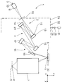
우선 마이크로리소그래피 투영 노광 장치(1)의 일반적인 구조와 주요 구성요소 부분의 예에 대한 설명이 이어진다. 일반적인 세부사항의 설명은 특히 제한적이지 않으며, 순전히 예시인 것으로서 이해되어야 한다.First, a general structure of the microlithography projection exposure apparatus 1 and an example of a main component portion are explained. The description of typical details is not to be taken in a limiting sense, and should be understood as purely illustrative.
도 1은 자오 단면에서 마이크로리소그래피 투영 노광 장치(1)를 개략적으로 도시한다. 투영 노광 장치(1)의 조명 시스템(2)은 방사선 소스(3) 이외에도, 대물 평면(6)의 대물 필드(5)의 노광을 위한 조명 광학 유닛(4)을 가진다. 대물 필드(5)는 직사각형 방식, 또는 예를 들어 13/1의 x/y 종횡비를 가지는 아치형 방식으로 형상화될 수 있다. 이 경우에, 대물 필드(5)에 배열된 반사 레티클(30)(도 1에 도시되지 않음)이 노광되고, 상기 레티클은 마이크로구조화된 또는 나노구조화된 반도체 구성요소의 생성을 위해서 투영 노광 장치(1)에 의해 투영될 구조를 보유한다. 투영 광학 유닛(7)은 영상 평면(9)의 영상 필드(8) 내로 대물 필드(5)를 영상화하는 역할을 한다. 레티클(30) 상의 구조는 웨이퍼의 감광층 상으로 영상화되고, 이는 도면에서 표현되지 않으며 영상 평면(9)의 영상 필드(8)의 구역 내에 배열된다.Figure 1 schematically shows a microlithographic projection exposure apparatus 1 in a meridional section. The illumination system 2 of the projection exposure apparatus 1 has, in addition to the
레티클 보유기(미도시)에 의해 보유되는 레티클(30)과 웨이퍼 보유기(미도시)에 의해 보유되는 웨이퍼는 투영 노광 장치(1)의 작동 중 y 방향으로 동기식으로 스캔된다. 투영 광학 유닛(7)의 영상화 스케일에 따라, 레티클(30)이 웨이퍼에 대해 대향하는 방향으로 스캔되는 것도 가능하다.The
방사선 소스(3)는 5nm와 30nm 사이의 범위에서 방출된 사용 방사선을 가지는 EUV 방사선 소스이다. 이는 플라즈마 소스, 예컨대 GDPP(Gas Discharge Produced Plasma) 소스나 LPP(Laser Produced Plasma) 소스일 수 있다. 다른 EUV 방사선 소스, 예컨대 싱크로트론이나 자유 전자 레이저(FEL, free electron laser)에 기초한 EUV 방사선 소스도 가능하다.The radiation source (3) is an EUV radiation source having radiation of use emitted in the range between 5 nm and 30 nm. Which may be a plasma source, such as a gas discharge produced plasma (GDPP) source or a laser produced plasma (LPP) source. Other EUV radiation sources are also possible, for example EUV radiation sources based on synchrotron or free electron laser (FEL, free electron laser).
이는 또한, 특히 200nm 미만의 파장을 가지는 방사선을 발생시키기 위한 VUV 방사선 소스일 수 있다.It may also be a VUV radiation source for generating radiation, in particular having a wavelength of less than 200 nm.
방사선 소스(3)로부터 나온 EUV 방사선(10)은 집광기(11)에 의해 집속된다. 대응하는 집광기가 예로서 EP 1 225 481 A로부터 알려져 있다. 집광기(11)의 하류에서, 필드 패싯 미러(13) 상에 입사되기 전의 EUV 방사선(10)이 중간 초점 평면(12)을 통해 전파된다. 필드 패싯 미러(13)는 대물 평면(6)에 대해 광학적으로 켤레인 조명 광학 유닛(4)의 평면에 배열된다.The EUV radiation (10) emerging from the radiation source (3) is focused by a concentrator (11). A corresponding concentrator is known, for example, from EP 1 225 481 A. Downstream of the
EUV 방사선(10)은 또한 이하에서 사용 방사선, 조명 광 또는 영상화 광으로 지칭된다. 사용 방사선은 또한, 특히 200nm 미만의 파장을 가지는 VUV 방사선일 수 있다.The
필드 패싯 미러(13)의 하류에서, EUV 방사선(10)은 동공 패싯 미러(14)에 의해 반사된다. 동공 패싯 미러(14)는 조명 광학 유닛(7)의 입사 동공 평면이나 그에 대한 광학 켤레 평면에 놓인다. 필드 패싯 미러(13) 및 동공 패싯 미러(14)는 다수의 개별 미러로 구성되며, 이는 아래에서 더욱 상세히 설명될 것이다. 이러한 경우에, 개별 미러로의 필드 패싯 미러(13)의 세분화는, 그들 자체로 전체 대물 필드(5)를 조명하는 각각의 필드 패싯(19)이 개별 미러 중의 정확히 하나로 표현되도록 이루어질 수 있다. 대안적으로, 복수의 그러한 개별 미러를 사용하여 필드 패싯(19)의 적어도 일부나 전체를 구성하는 것이 가능하다. 동일한 내용이 동공 패싯 미러(14)의 동공 패싯(20)의 구성에 대응하여 적용되며, 이는 각각 필드 패싯(19)에 할당되고 단일 개별 미러 혹은 복수의 그러한 개별 미러에 의해 각각의 경우에 형성될 수 있다.Downstream of the
EUV 방사선(10)은 25°보다 작거나 그에 동일한 입사 각도로 두 개의 패싯 미러(13, 14) 상에 충돌한다. EUV 방사선(10)은 그러므로 수직 입사 작동 범위에서 두 개의 패싯 미러 상에 충돌한다. 스침 입사에 의한 충돌이 또한 가능하다. 동공 패싯 미러(14)는, 투영 광학 유닛(7)의 동공 평면을 구성하거나 투영 광학 유닛(7)의 동공 평면에 대해 광학적으로 켤레인 조명 광학 유닛(4)의 평면에 배열된다. EUV 방사선(10)에 대한 비임 경로의 순서로 지정된 미러(16, 17, 18)를 가지는 전송 광학 유닛(15) 형태의 영상화 광학 조립체 및 동공 패싯 미러(14)의 도움에 의해, 필드 패싯 미러(13)의 필드 패싯(19)은 이들이 서로에 대해 중첩되는 방식으로 대물 필드(5) 상에 영상화된다. 전송 광학 유닛(15)의 마지막 미러(18)는 스침 입사를 위한 미러("스침 입사 미러")이다. 동공 패싯 미러(14)와 함께, 전송 광학 유닛(15)은 대물 필드(5)를 향해 필드 패싯 미러(13)로부터 EUV 방사선(10)을 전송하기 위한 순차 광학 유닛으로서도 지칭된다. 조명광(10)은 복수의 조명 채널을 통해 방사선 소스(3)로부터 대물 필드(5)를 향해 안내된다. 각각의 이러한 조명 채널은 필드 패싯 미러(13)의 필드 패싯(19) 및 동공 패싯 미러(14)의 동공 패싯으로 할당되고, 상기 동공 패싯은 필드 패싯의 하류에 배치된다. 필드 패싯 미러(13) 및 동공 패싯 미러(14)의 개별 미러는, 필드 패싯(19)에 대한 동공 패싯(20)의 할당에서의 변화와, 대응하여 조명 채널에서의 변화된 구성이 달성될 수 있도록, 액추에이터 시스템에 의해 틸팅가능하게 될 수 있다. 이는 대물 필드(5)에 걸쳐 이루어지는 조명광(10)의 조명 각도의 분포가 구별되는, 다양한 조명 설정을 야기한다.The
위치적 상관관계의 설명을 용이하게 하기 위해, 아래에서 특히 글로벌 데카르트 xyz-좌표 시스템이 사용된다. x 축은 도 1에서 관찰자를 향해 도면의 평면에 수직하게 진행한다. y 축은 도 1에서 우측을 향해 진행한다. z 축은 도 1에서 상방으로 진행한다.To facilitate describing the positional correlation, the global Cartesian xyz-coordinate system is used below. The x-axis travels perpendicularly to the plane of the figure toward the observer in Fig. The y-axis travels to the right in Fig. The z-axis advances upward in Fig.
다양한 조명 설정은, 필드 패싯 미러(13)의 개별 미러의 대응하는 틸팅 및 동공 패싯 미러(14)의 개별 미러에 대한 필드 패싯 미러(13)의 상기 개별 미러의 할당에서의 대응하는 변화에 의해 달성될 수 있다. 필드 패싯 미러(13)의 개별 미러의 틸팅에 따라, 상기 개별 미러에 새롭게 할당된 동공 패싯 미러(14)의 개별 미러는 필요하다면 대물 필드(5)로의 필드 패싯 미러(13)의 필드 패싯(19)의 영상화가 다시 한 번 보장되도록 하는 틸팅에 의해 추적된다.The various illumination settings are achieved by corresponding tilting of the individual mirrors of the
다중 혹은 마이크로 미러 어레이(MMA) 형태의 필드 패싯 미러(13)는 사용 방사선(10), 즉 EUV 방사선 비임을 안내하기 위한 광학 조립체를 형성한다. 필드 패싯 미러(13)는 마이크로전자기계 시스템(MEMS)으로 형성된다. 이는 어레이의 행과 열으로 행렬형 방식으로 배열된 다수의 개별 미러(27)를 가진다. 개별 미러(27)는 아래에서 설명되는 바와 같이 액추에이터 시스템에 의해 틸팅가능하도록 설계된다. 전체적으로, 필드 패싯 미러(13)는 대략 100000개의 개별 미러(27)를 가진다. 개별 미러(27)의 크기에 따라, 필드 패싯 미러(13)는 또한 예컨대 1000, 5000, 7000개, 그렇지 않으면 특히 적어도 100000개, 특히 적어도 300000개, 특히 적어도 500000개의, 수십만 개의 개별 미러(27)를 가질 수 있다.A
투영 노광을 위해 사용가능하지 않은 방사선 소스(3)의 다른 방출 파장 성분으로부터 사용 방사선(10)을 분리하는 스펙트럼 필터가 필드 패싯 미러(13)의 상류에, 즉 필드 패싯 미러(13)와 방사선 소스(3) 사이에 배열될 수 있다. 스펙트럼 필터는 표현되지 않는다.A spectral filter which separates the used
840W의 전력과 6.5 kW/m2의 전력 밀도를 가지는 사용 방사선(10)이 필드 패싯 미러(13) 상에 충돌한다. 일반적으로, 다른 전력 및 전력 밀도 또한 가능하다. 전력 밀도는 적어도 500W/m2, 특히 적어도 1kW/m2, 특히 적어도 5kW/m2, 특히 적어도 10kW/m2, 특히 적어도 60kW/m2이다.
패싯 미러(13)의 전체 개별 미러 어레이는 500mm의 직경을 가지며, 개별 미러(27)와 조밀 패킹 방식으로 설계된다. 필드 패싯(19)이 각 경우에 정확히 하나의 개별 미러로 실현되기만 한다면, 개별 미러(27)는 스케일링 인자와 별도로 대물 필드(5)의 형상을 표현한다. 패싯 미러(13)는 각각 필드 패싯(19)을 표현하고 y 방향에서 대략 5mm, 그리고 x 방향에서 100mm의 치수를 가지는 500개의 개별 미러(27)로부터 형성될 수 있다. 정확히 하나의 개별 미러(27)에 의한 각 필드 패싯(19)의 실현예에 대한 대안으로서, 각각의 필드 패싯(19)은 더 작은 개별 미러(27)의 그룹에 의해 근사화될 수 있다. y 방향에서 5mm, 그리고 x 방향에서 100mm의 치수를 가지는 필드 패싯(19)은 예컨대 5mm×5mm의 치수를 가지는 개별 미러(27)의 1×20 어레이 내지는 0.5mm×0.5mm의 치수를 가지는 개별 미러(27)의 10×200 어레이에 의해 구성될 수 있다. 미러 표면의 더욱 복합적인 분할이 가능하다. 개별 미러(27)는 특히 개별적으로 틸팅될 수 있다. 개별 미러(27)에 의한 완전한 필드 패싯 어레이의 영역 커버리지는 적어도 70%, 특히 적어도 80%, 특히 적어도 90%일 수 있다.The entire individual mirror array of the
사용광(10)은 동공 패싯 미러(14)를 향해서 패싯 미러(13)의 개별 미러(27)에 의해 반사된다. 동공 패싯 미러(14)는 대략 2000개의 정적 동공 패싯(20)을 가진다. 제일 안쪽의 링의 동공 패싯(20)이 부채꼴 형상의 방식으로 제작되고 그에 바로 인접한 링의 동공 패싯(20)은 링-부채꼴 형상의 방식으로 제작되도록, 정적 동공 패싯은 복수의 동심 링에서 서로의 옆에 배열된다. 동공 패싯 미러(14)의 사분면에서, 12개의 동공 패싯(20)은 각각의 링에서 서로의 옆에 존재할 수 있다. 동공 패싯(20)은 각 경우에 단순히 연결된 방식으로 형성될 수 있다. 동공 패싯(20)의 일부 다른 배열이 마찬가지로 가능하다. 또한 이들은 다수의 개별 미러(27)에 의해 형성될 수 있다. 동공 패싯 미러(14)는 특히 다수의 개별 미러(27)를 가지는 다중-미러 어레이(MMA, multi-mirror array)로서도 형성될 수 있다. 이는 특히 MEMS로서 형성될 수 있다. 이는 일반적으로 제2 패싯 미러를 형성한다.The used
사용광(10)은 대물 평면(6)에 배열된 반사 레티클(30)을 향해서 동공 패싯(20)에 의해 반사된다. 그 다음, 위에서 설명된 바와 같이, 투영 광학 유닛(7)이 이에 후속된다.The used
필드 패싯 미러(13)와 동공 패싯 미러(14)의 개별 미러(27)는 사용 방사선(10)의 파장에서 그의 반사성을 최적화 하기 위해 다중층 코팅을 포함한다. 다중층 코팅의 온도는 투영 노광 장치(1)의 작동 중 425K를 초과해서는 안된다.The
개별 미러(27)의 구조의 세부사항과 이들의 변위성에 대하여, WO 2010/049 076 A1을 참조해야 한다. 이 공보는 본 출원에서 구성요소 부분으로서 그 전체 범위가 포함되어 있다.For details of the structure of the individual mirrors 27 and their displacements, see WO 2010/049 076 A1. This publication contains the entire range of the component parts in this application.
조명 광학 유닛(4)은 배기가능 챔버(32) 내에 수용되고, 그의 경계 벽(33)은 도 1에 나타난다. 챔버(32)는 유체 라인(26)을 통해서 차단 밸브(28)가 수용된 진공 펌프(31)와 연통한다. The illumination
배기가능 챔버(32)에서의 작동 압력은 몇 Pa(H2의 분압)이다. 수소의 분압은 특히 최대 50Pa, 특히 최대 20Pa, 특히 최대 10Pa, 특히 최대 5Pa이다. 모든 다른 분압들은 1x10- 7mbar의 상당히 아래에 있다. 챔버(32)는 특히 고진공 또는 초고진공까지 배기될 수 있다.The operating pressure in the
배기가능한 챔버(32)와 함께, 복수의 개별 미러(27)를 가지는 미러는 EUV 방사선(10) 묶음을 안내하기 위한 광학 구성요소의 구성요소 부분이다. 개별 미러(27)는 패싯 미러(13, 14) 중 하나의 부품일 수 있다.A mirror with a plurality of
각각의 개별 미러(27)는 0.5mm×0.5mm, 그렇지 않으면 5mm×5mm, 또는 보다 큰 치수를 가지는 충돌가능한 반사 표면(34)을 가질 수 있다. 반사 표면(34)은 개별 미러(27)의 미러 본체(35)의 부품이다. 미러 본체(35)는 다중층 코팅을 포함한다. 개별 미러(27) 또는 그의 반사 표면(34)은 또한 다른 치수를 가질 수 있다. 이들은 특히 타일으로 형성되며, 2-차원 표면 영역은 타일에 의해 모자이크식이 될 수 있다. 이들은 특히 삼각형, 사각형, 특히 정사각형, 또는 육각형 방식으로 형성될 수 있다. 이들의 측부 길이는 특히 최대 10mm, 특히 최대 5mm, 특히 최대 3mm, 특히 최대 1mm, 특히 최대 0.5mm, 특히 최대0.3 mm, 특히 최대 0.1mm의 치수를 가진다. 이들은 결과적으로 특히 마이크로-미러일 수 있다. 이는 특히 마이크로미터 범위의 치수를 가지는 미러로서 이해되어야 한다.Each
개별 미러(27)는 각 경우에, 다수의 전자기적으로, 특히 정전식으로 작동하는 액추에이터를 가지는 액추에이터 디바이스에 의해 변위가능, 즉 위치설정가능하다. 액추에이터는 마이크로전자기계 시스템(MEMS)으로서 일괄 프로세스에서 생성될 수 있다. 세부사항에 대해, WO 2010/049 076 A1을 다시 한 번 참조해야 한다.The individual mirrors 27 are in each case displaceable, i.e. positionable, by means of an actuator device having a plurality of electromagnetic, in particular electrostatically actuated, actuators. Actuators can be created in a batch process as microelectromechanical systems (MEMS). For details, see WO 2010/049 076 A1 again.
미러 본체(35) 상의 반사 표면(34)의 합은 필드 패싯 미러(13)의 전체 반사 표면에 의해 커버되는 합계 표면 영역의 0.5배 보다 크다. 합계 표면 영역은 이 경우 반사 표면 영역(34)과, 반사 표면 영역(34)들 사이의 사이공간에 의해 커버되는 영역이 더해진 합계로서 규정된다. 한편으로 이러한 합계 표면 영역에 대한 미러 본체의 반사 표면의 합계의 비율은 또한 집적 밀도로서 지칭된다. 이러한 집적 밀도는 또한 0.6보다 크고, 특히 0.7보다 크고, 특히 0.8보다 크고, 특히 0.9보다 클 수 있다.The sum of the
투영 노광 장치(1)의 도움에 의해, 레티클(30)의 적어도 하나의 부분이 마이크로 또는 나노구조화된 구성요소, 특히 반도체 구성요소, 예컨대 마이크로칩의 마이크로리소그래피 생성을 위해 웨이퍼 상의 감광층의 구역 상으로 영상화된다. 스캐너 또는 스테퍼로서의 투영 노광 장치(1)의 실시예에 따라, 레티클(30)과 웨이퍼는 스테퍼 작동 시 단계식으로, 또는 스캐너 작동 시 연속적으로 y 방향에서 일시적으로 동기화된 방식으로 이동한다.With the aid of the projection exposure apparatus 1, at least one portion of the
조명 광학 유닛(4)은 바람직하게는 고진공 또는 초고진공에서 작동된다. 플라즈마(45), 특히 수소 플라즈마는 개별 미러(27) 앞의, 특히 반사 표면(34)을 가지는 미러 본체(35) 앞의 구역에서 형성될 수 있다. 플라즈마(45)는 특히 사용 방사선(10)의 고-에너지 광자에 의해 생성될 수 있다. 플라즈마(45)의 속성은 결과적으로 방사선 소스(3)의 속성, 특히 그의 작동 모드, 특히 그의 펄스 주파수 및/또는 펄스 지속시간 및/또는 강도, 그리고 챔버(32)의 대기에도 의존한다.The illumination
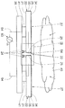
다중-미러 어레이(29)(MMA)로 형성된 패싯 미러(13)의 추가적인 세부사항의 설명이 이어진다. 다중-미러 어레이(29)는 일반적으로 다수의 개별 미러(27)의 미러 디바이스를 형성한다. 개별 미러(27)는 지지 구조물(36) 상에 배열된다. 세부사항에 대하여, 특히 WO 2010/049976 A1을 참조해야 한다.A further description of the
미러 디바이스는 일반적으로 적어도 하나의 미러(27)를 포함한다. 다중-미러 어레이(29)(MMA)의 개별 미러(27)의 개수는 1로부터 1000000까지의 범위에 놓인다. 또한 이론적으로는 이보다 클 수 있다. 이는 이론적으로는 요구사항에 따라 자유롭게 선택가능하다.The mirror device generally comprises at least one
개별 미러(27)는 적어도 80mrad, 특히 적어도 100mrad, 특히 적어도 120mrad만큼 각각의 반경방향에서 피봇될 수 있다. 이들은 특히 적어도 2 변위 자유도, 특히 적어도 2 피봇 자유도를 가진다.The individual mirrors 27 can be pivoted in their respective radial directions by at least 80 mrad, in particular by at least 100 mrad, in particular by at least 120 mrad. They have in particular at least two displacement degrees of freedom, in particular at least two pivot degrees of freedom.
마이크로 미러로서 형성된 개별 미러(27)는 미세한 굴곡 구조 상에 현수된다. 미세한 굴곡 구조는 얇은 실리콘 웨이퍼 또는 금속 멤브레인 등으로부터 절삭되거나 에칭된다. 굴곡 구조는 특히 2-차원, 즉 멤브레인 방식으로, 또는 비임 형식이나 카르단식(cardanically)으로 형성될 수 있다.The individual mirrors 27 formed as micromirrors are suspended on the fine bending structure. The fine bending structure is cut or etched from thin silicon wafers or metal membranes. The bending structure can be particularly formed in two-dimensional, i.e. membrane-based, or beam-form or cardanically.
개별 미러(27)는 액추에이터 시스템에 의해 변위가능하다. 동작은 바람직하게는 정전식이거나 전기기계식이거나 압전식이다. 이에 대한 대안이 마찬가지로 가능하다.The individual mirrors 27 are displaceable by an actuator system. The operation is preferably electrostatic, electro-mechanical or piezoelectric. An alternative to this is likewise possible.
다중-미러 어레이(29)(MMA)는 마이크로구조화에 의해, 특히 마이크로전자기계 구조화 단계의 시퀀스에 의해, 특히 예를 들어 리소그래피 단계, 퇴적, 본딩 또는 성형과 같은 방법 단계를 사용하여 생성된다. 이는 특히 프로세싱 후에 서로 본딩된 다수의 개별 웨이퍼로부터 생성된다. 세부사항들이 아래에서 더욱 구체적으로 설명된다.The multi-mirror array 29 (MMA) is created by microstructuring, in particular by a sequence of microelectromechanical structuring steps, in particular using method steps such as, for example, lithography steps, deposition, bonding or molding. This is especially generated from a number of individual wafers bonded together after processing. The details are described in more detail below.
전기적 연결, 특히 회로가 다음과 같이 생성된다: 수평하게 진행하는 것들, 즉 웨이퍼 표면에 평행한 방향으로 진행하는 것들은 개별 웨이퍼의 표면에 얇은 금속성 또는 도핑된 반도체 층으로 적용될 수 있다. 프린팅 또는 증착 프로세스는 이를 위해 제공될 수 있다. 수직 전기 연결부, 즉 웨이퍼, 예컨대 지지 구조물(36)을 통과하여 연장하는 연결부는 예를 들어 소위 관통 실리콘 비아로 생성될 수 있다. 마이크로전자기계 구조화 단계를 가지는 방법(MEMS 방법)이 이를 위해 제공될 수 있다. 구조화 단계는 특히 기판의 함몰부, 특히 트렌치를 생성하기 위한 에칭 단계, 그리고 특히 예를들어 금속 또는 도핑된 반도체 재료와 같은 전기 전도성 재료로 트렌치를 후속 충전하는, 또는 전기 절연 재료로 충전하는 단계를 포함한다.Electrical connections, in particular circuits, are created as follows: those running in a horizontal direction, that is, those traveling in a direction parallel to the wafer surface, can be applied as a thin metallic or doped semiconductor layer to the surface of an individual wafer. A printing or deposition process may be provided for this. A vertical electrical connection, i. E., A connection extending through the wafer, e.g., the
반사 표면(34)은 미러 본체(35)의 전방으로 향하는 전방 측부 상에 배열된다. 이는 특히 전방 측부를 형성한다. 개별 미러(27)의 반사 표면(34)으로부터 대향하는 미러(35)의 측부는 미러 본체(27)의 후방 측부(21)로 지칭된다. 이하에서 사용되는 "전방" 및 "후방"의 방향 지시는 미러 본체(35)의 전방 및 후방 측부의 정렬에 관한 것이다. 이들은 특히 위치적 상관관계의 더 용이한 설명을 위해 사용된다.The
반사 표면(34)은 정사각형 방식으로 형성된다. 이는 일반적으로 바람직하게는 사변형, 특히 평행사변형, 특히 직사각형 또는 육각형 방식으로 형성된다. 이는 또한 이론적으로 대안적인 기하학적 형태를 가질 수 있다. 이는 특히 미러 디바이스의 전체 반사 표면이 실질적으로 어떠한 간극도 없이 개별 미러(27)에 의해 모자이크화될 수 있는 방식으로 형성된다.The
미러 본체(35) 각각은 네 개의 측부 표면(22)을 가진다. 측부 표면(22)은 각각 미러 본체(35)의 전방 측부와 미러 본체의 후방 측부(21) 사이에서 진행한다. 이들은 특히 미러 본체(35)의 전방 및 후방 측부(21)에 대해 수직하게 진행한다. 이들은 또한 이들 측부에 대해 경사지게 진행할 수 있다. 이 경우에, 미러 본체(35)는 절두피라미드 방식으로 형성된다.Each of the
도 2에 도시된 실시예의 경우에, 스페이서(41)가 미러 본체(35)와 지지 구조물(36) 사이에 배열된다. 스페이서(41)는 또한 미러 현수체로서 역할을 한다. 미러 현수체는 기부 판으로부터 고정된 거리에서 미러의 피봇점을 고정시킨다.In the case of the embodiment shown in FIG. 2,
일반적으로, 다중-미러 어레이(29)는 마이크로전자기계 시스템(MEMS)으로서 형성된다. 개별 미러(27)는 유연하게, 특히 피봇가능하게 장착된다. 개별 미러(27)의 후방 측부(21) 뒤의 구역에서, 전자 회로, 특히 액추에이터 및/또는 센서 회로가 특히 개별 미러(27)의 변위를 제어하기 위해 제공된다. 회로는 특히 주문형 집적 회로(ASICs)로서 형성된다. ASIC는 지탱 구조물의 후방 측부 상으로 본딩된다. 액추에이터 또는 센서와 ASIC 사이의 전기 라인은 지탱 구조물(36)을 통해 진행한다. ASIC는 특히 캡슐화된 구역, 특히 외부로부터 밀폐 방식으로, 특히 진공 밀폐 방식으로 밀봉된 구역에 배열될 수 있다. 이들은 특히, 이들이 진공 환경에서 사용될 수 있는 방식으로 형성 및/또는 배열된다.Generally, the
다중-미러 어레이의 추가적인 세부사항의 설명이 후속하며, 이들은 특히 조명 방사선에 의해 생성될 수 있는 대전된 입자로부터 특히 전자 장치, 특히 미러 뒤의 전자 구성요소, 특히 회로 및/또는 액추에이터 시스템 및/또는 센서 시스템, 그리고 또한 가능하게는 ASIC를 보호하는 역할을 한다. 특히 조명 방사선(10)에 의해 생성된 플라즈마(45)가 개별 미러(27)들 사이를 통해 관통하는 것과 미러 본체(35)의 후방 측부(21) 뒤에 배열된 전자장치, 특히 센서 및/또는 액추에이터 및/또는 그의 신호 라인에 영향을 미치는 것을 방지하는 수단이 제공된다.This is followed by a description of additional details of a multi-mirror array, in particular from the charged particles which can be generated by illumination radiation, in particular electronic components, in particular electronic components behind mirrors, in particular circuit and / or actuator systems and / Sensor systems, and possibly also ASICs. In particular in the case of an electronic device, in particular a sensor and / or actuator, arranged behind the
본 발명에 따라 제공된 수단의 효율성이 검증될 수 있고, 특히 분석적으로 그리고 시뮬레이션에 의해 검증된다.The efficiency of the means provided in accordance with the invention can be verified, particularly verified analytically and by simulation.
일반적으로 미러 본체(35)의 전방 측부 앞의 체적 구역으로부터 미러 본체의 후방 측부(21) 뒤의 구역 내로의 대전된 입자의 관통은 미러 본체(35)의 측부 표면(22)들 사이의 구역에서 전기 필드(23)를 생성함으로써 방지될 수 있다는 것이 인식되었다.The penetration of charged particles into the area behind the
본 발명에 따라, 전기 필드에서의 대전된 입자의 궤적은 그의 운동 에너지, 그의 펄스 및 전기 필드 강도의 분포로부터 결정될 수 있다는 것이 인식되었다. 또한 알려진 최대 운동 에너지를 가지는 대전 입자가 미러 본체(35)의 전방 측부 앞의 구역으로부터 미러 본체(35)의 후방 측부(21) 뒤의 구역 내로 통과하는 것을 방지하는 것이 필드(23)의 전기 필드 강도의 적절한 적응에 의해 가능하다는 것이 인식되었다.It has been recognized, in accordance with the present invention, that the trajectory of charged particles in an electric field can be determined from its kinetic energy, its pulse and its distribution of electric field strength. It is also advantageous to prevent the charged particles with a known maximum kinetic energy from passing through the area in front of the front side of the
미러 본체(35)의 두께(d), 특히 차폐 전극(25) 그리고 또한 인접한 미러 본체(35)들 사이의 거리(g)의 대응하는 범위, 조명 방사선(10)의 광자의 알려진 에너지(Eph)(EUV에 대하여 Eph=91.8eV), 또한 챔버(32)의 가스 입자의 이온화 에너지(Eion)(H2에 대하여 Eion=15.4eV)에 따라, 효율적으로 이온화된 입자를 감속하기 위해서 전압(Ur)이 얼마나 커야하는지를 결정할 수 있다. 50V 내지 100V의 크기 정도의 전압(Ur)이, 대전된 입자가 플라즈마(45)로부터 미러 본체(35)의 후방 측부(21) 뒤의 구역 내로 통과하는 것을 방지하기에 충분하다는 것이 발견되었다.The thickness d of the
후속하는 추산치가 특히 플라즈마로부터 미러 본체(35)의 후방 측부(21) 뒤의 구역 내로의 대전된 입자의 관통을 방지하기 위해 필요한 전압(Ur)에 대해 획득되었고:The following estimates were obtained for the voltage (U r ) necessary to prevent the penetration of charged particles into the area behind the

여기서, e는 기본 전하를 나타낸다.Here, e represents a basic charge.
이러한 추산치는 미러 본체(35)의 측부 표면(22) 사이의 사이공간(54)의 구역에서의 전기 필드(23)는 최대한 균일하다는 가정에 기초한다. 현실적인 시뮬레이션에 의해 이것이 상당한 근사도로 정확하다는 것을 보여줄 수 있다. 필드 라인의 예시적인 분포가 도 3a 및 도 3b에 도시된다. 여기서 한 쌍의 콤 전극(24)이 각 경우에 개별 미러(27)의 변위를 위한 역할을 한다는 것이 가정되었다. 콤 전극(24)은 각각 20μm·20μm의 치수를 가진다. 이들은 각 경우에 미러 본체(35)의 후방 측부(21) 상에 배열된다. 이들은 특히 미러 본체(35)의 측부 표면(22)의 구역에 배열된다. 200V의 최대 전압이 이들에게 적용되는 것이 시뮬레이션에 대해서 가정된다.These estimates are based on the assumption that the
또한 미러 본체(35)가 이들의 전방 및 후방 측부(21)에 평행한 방향으로 600μm의 치수, 70μm의 두께(d)를 가지며, 스페이서(41) 상의 지지 구조물(36)으로부터 50μm의 거리에서 유지된다는 것이 시뮬레이션에 대해서 가정된다. 스페이서(41)는 140μm의 직경을 가진다. 인접한 미러 본체(35)들 사이의 거리(g)는 35μm이다. 이러한 치수들은 대응하는 미러 디바이스의 실제 조건에 대응한다. 이들은 제한적인것으로 이해되어서는 안된다. 미러의 대안적인 실시예에 대해, 특히 1mm의 치수를 가지는 미러 본체에 대해서 본 발명에 따라 제공된 차폐 요소의 적응은 어떠한 문제도 없이 가능하다.The
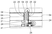
도 2에 도시된 바와 같은 예시적 실시예의 경우에, 미러 본체(35)의 측부 표면(22)들 사이의 구역에서 전기 필드(23)를 생성하기 위해서, 차폐 전극(25)은 각각 측부 표면(22)의 구역에 배열된다. 차폐 전극(25)은 각 경우에 실질적으로 미러 본체(35)의 전체 측부 표면(22)에 걸쳐, 특히 그의 전체 두께(d)에 걸쳐 연장한다. 반면에, Ur에 대한 공식에서, 전술한 d는 미러 본체(35)의 두께의 범위의 방향에서 차폐 전극(25)의 범위를 나타낸다.2, the shielding
미러 본체(35)의 측부 표면(22)에 대한 차폐 전극(25)의 표면 영역의 비율은 특히 적어도 0.5, 특히 적어도 0.7, 특히 적어도 0.8, 특히 적어도 0.9, 특히 적어도 0.95, 특히 적어도 0.99이다.The ratio of the surface area of the
전압 소스(63)는 차폐 전극(25)에 차폐 전압(Ur)을 적용시키기 위해 제공된다. 전압 소스(63)는 도면에서 오직 개략적으로 나타내어진다. 이는 다중-미러 어레이(29)의 구성요소 부분일 수 있다. 이는 특히 지지 구조물(36)의 구역에 배열될 수 있다. 이는 또한 외부 전압 소스일 수 있다.A
전압 소스(63)는 전기 공급 라인(64)에 의해 차폐 전극(25)에 연결된다. 전기 공급 라인(64)은 미러 본체(35)와 지지 구조물(36)에 적어도 부분적으로 배열된다.The
도 3a는 인접한 개별 콤 미러(27)들의 콤 전극(24)이, 이들이 생성한 전기 필드가 각각의 미러 본체(35)의 측부 표면(22)들 사이의 전기 필드(23)에 실질적으로 대향하게 정렬되는 방식으로 동작되는 경우를 도시한다. 도 3b는 콤 전극(24)에 의해 생성된 전기 필드가 대응하는 미러 본체(35)의 측부 표면(22)들 사이의 구역에서 차폐 전극(25)에 의해 생성된 전기 필드(23)와 같은 방향으로 지향하는 경우를 도시한다.3a shows that the
도 3a 및 3b에서 정성적으로 알 수 있는 바와 같이, 콤 전극(24)에 의해 생성된 전기 필드는 인접한 개별 미러(27)의 측부 표면(22)들 사이의 구역에서 전기 필드(23)의 전기 필드 강도의 분포에 대하여, 만일 있다면, 언급된 조건하에서 무시할만한 영향을 가진다. 이러한 구역에서의 전기 필드(23)는 차폐 전극(25)에 적용된 전압(Ur)에 의해 지배된다. 80V의 차폐 전압(Ur)은 개별 미러(27)의 후방 측부(21) 뒤의 체적 구역의 완전 전기 차폐를 초래한다. 차폐 전극(25)에 의해 생성된 전기 필드(23)는 실질적으로 인접한 개별 미러(27)의 측부 표면(22) 사이의 구역으로 제한된다. 차폐 전압(Ur)을 적용시키는 것은 평행 등전위 라인의 플래토를 생성하는 효과를 가진다. 전기 필드(23)는 즉 개별 미러(27)의 반사 표면(34)에 평행하며 균일한 것으로서 간주될 수 있다. 미러 본체(35)의 전방 측부 앞의 구역 내로 도달하는 전기 필드(23)는 이러한 구역의 대전된 입자에 대한 효과에 영향을 미칠 수 있지만, 이는 이들의 운동 에너지에서의 유의한 증가를 초래하지 않을 것이다. 즉, 도 3a 및 도 3b의 예로서 표현된 상황은 콤 전극(24)으로의, 그리고 일반적으로 미러 본체(35)의 후방 측부(21) 뒤의 구역 내로의 플라즈마(45)의 어떠한 누출도 초래하지 않는다.3A and 3B, the electric field generated by the
또한, 이는 인접한 개별 미러(27) 중 하나 또는 양쪽 모두가 피봇된 위치, 특히 최대로 피봇된 위치에 있는 경우에도 적용된다는 것을 보여줄 수 있다.It can also be shown that this applies even if one or both of the adjacent individual mirrors 27 are in a pivoted position, in particular in a maximally pivoted position.
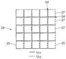
도 4를 참조로 하여 차폐 요소의 추가적인 세부사항, 특히 다중-미러 어레이(29)의 차폐 전극(25)의 배열의 설명이 이어진다.With reference to FIG. 4, further details of the shielding element will follow, particularly a description of the arrangement of the shielding
플라즈마를 차폐(25)하기 위해 전기 필드(23)가 각각의 모든 인접한 개별 미러(27)들 사이에서 생성될 수 있는 방식으로 개별 미러(27)의 미러 본체(35)의 측부 표면(22)의 구역에 차폐 전극(25)이 배열된 다중-미러 어레이(29)의 개별 미러(27)의 배열체가 도 4의 예시에 의해 도시된다.It is preferred that the
차폐 전극(25)은 각각 인접한 개별 미러(27)의 상호 대향하는 측부 표면(22)의 구역에서 쌍으로 배열된다. 이들은 각 경우에 인접한 개별 미러(27) 사이의 구역에서 전기 필드(23)를 구축하는 역할을 한다.The shielding
도 4에서, 상이한 전압(Ur)이 차폐 전극(25)에 적용되었다는 것이 개략적으로 나타내어진다. 제1 전압(Ur1)은 차폐 전극(25)의 제1 부분집합에 적용된다. 제2 전압(Ur2)은 차폐 전극(25)의 제2 부분집합에 적용된다. 이러한 경우에, Ur1≠Ur2, 특히 |Ur1-Ur2|≥10V, 특히 |Ur1-Ur2|≥20V, 특히 |Ur1-Ur2|≥30V, 특히 |Ur1-Ur2|≥40V, 특히 |Ur1-Ur2|≥50V, 특히 |Ur1-Ur2|≥70V, 특히 |Ur1-Ur2|≥100V가 참이 된다. 특히 |Ur1-Ur2|≤300V, 특히 |Ur1-Ur2|≤200V, 특히 |Ur1-Ur2|≤100V가 참이 된다.In Fig. 4, it is schematically shown that a different voltage U r is applied to the
도 4에 도시된 바와 같은 배열의 경우에, 미러 본체(35)의 서로에 대해 인접한 측부 표면(22)에서의 두 개의 차폐 전극(25)은 각각 등전위이며, 즉 동일한 차폐 전위가 이들에게 적용되었다.In the case of the arrangement as shown in Fig. 4, the two shielding
도 4에 도시된 바와 같은 배열체의 경우, 차폐 전극(25)에 대한 전기 전압의 적용은 특히 모든 개별 미러(27)가 특정 차폐 전위를 가지는 차폐 전극(25)의 동일한 배열을 가지도록 선택된다. 특히, 도 4에서 하방으로 그리고 좌측으로 표시된 개별 미러의 차폐 전극(25)은 각 경우에 제1 전위(Ur1)를 가진다. 상방으로 그리고 우측으로 표시된 차폐 전극(25)은 각 경우에 제2 전위(Ur2≠Ur1)에서 유지된다. 바람직한 실시예에 따라, 상이한 차폐 전위는 동일한 크기를 가지지만 반전된 극성을 가진다(Ur1=-Ur2).In the case of an arrangement as shown in Figure 4, the application of the electric voltage to the
개별 미러(27)의 다른 배열, 즉 차폐 전극(25)에 각각 적용되는 차폐 전위가 마찬가지로 가능하다. 예컨대, 도 4에 도시된 바와 같은 배열로부터 시작하여, 90° 반시계 방향으로 제2, 제4, 제6, …제(2n) 행의 각각의 개별 미러(27)를 회전하는 것이 가능하다. 또한 90° 시계 방향으로 제2, 제4, 제6, …제(2n) 열의 각각의 개별 미러(27)를 회전하는 것이 마찬가지로 가능하다.Shielding potentials applied to other arrangements of the individual mirrors 27, i.e., the shielding
또한 각각의 경우에 각 개별 미러(27)의 상호 대향하는 차폐 전극(25)에 동일한 차폐 전위를 적용시키는 것이 가능하다. 이러한 경우에, 행 또는 열의 인접한 개별 미러(27)는 각각 이들이 서로에 대해 90°로 회전되도록 배열된다.It is also possible in each case to apply the same shielding potential to mutually opposing shielding
어떤 배열이 선택되는가는 전기 아키텍쳐, 차폐 케이블 및 공급 라인의 가능한 배열에 달려있다. 다중-미러 어레이(29)를 생성하기 위한 방법의 도 5 내지 도 12를 참조하는 설명이 이어진다. 도면에서, 다중-미러 어레이(29)의 두 개의 개별 미러(27)의 세부사항만이 각 경우에 표시된다. 전체 다중-미러 어레이(29)는 더 클 수 있다. 이는 특히 개별 미러(27)가 있는 다수의 행과 열을 포함할 수 있다. 도면에서, 상이한 개별 방법 단계 후, 중간 생성물의 위로부터의(좌측 열), 단면에서의(중간 열) 도면, 그리고 아래로부터의(우측 열) 도면이 예로서 각각 표현된다. 도면에서, 상이한 재료는 상이한 종류의 해칭으로 표현되었다.Which arrangement is chosen depends on the possible arrangement of the electrical architecture, the shielded cable and the supply line. A description will follow with reference to Figs. 5 to 12 of a method for generating a
도면은 플라즈마 환경에서 사용하기에 적합한 MEMS 다중-미러 어레이(29)를 생성하기 위한 방법 단계의 가능한 시퀀스를 도시한다. 이를 위해 필수적인 전제조건은, 내부 전기 구성요소, 특히 회로, 액추에이터, 센서 그리고 또한 특히 ASIC가 교란되지 않고 작동하는 것이다. 이들은 특히 플라즈마 환경으로부터의 자유 전하로부터 보호되어야 한다.The figure shows a possible sequence of method steps for creating a MEMS
도 5 내지 도 8은 세 개의 상이한 전기 전위가 반사 표면(34)과 또한 각각의 경우에 두 쌍의 인접한 측부 표면(22)에 적용되는 다중-미러 어레이(29)를 생성하기 위한 방법 단계의 시퀀스를 보여준다. 도 5 내지 도 8은 상이한 전압이 각각 개별 미러(27)의 전방 측부와 각각의 경우에 두 쌍의 각각 인접한 측부 표면(22)에 적용되는 방식으로 형성되는 다중-미러 어레이(29)를 생성하기 위한 방법 단계의 시퀀스를 예로서 보여준다. 도 9 내지 도 12는 한 쌍의 측부 표면(22)에 적용된 것과 같은 전위가 개별 미러(27)의 전방 측부에 적용되는 대안례를 도시한다. 방법 단계의 시퀀스는 실질적으로 동일하며 그러므로 둘 모두의 대안례에 대해 함께 설명된다. 임의의 차이점이 지적된다.5 through 8 illustrate a sequence of method steps for creating a
먼저, 미러 웨이퍼(46)의 생성은 도 5 및 도 9를 참조로 설명된다. 미러 웨이퍼(46)의 생성을 위해서, 제1 이중 SOI 웨이퍼(47)(silicon-on-isolator wafers)가 제공된다(1-0). SOI 웨이퍼(47)의 도핑은 미러의 원하는 전기 저항에 달려있다. 이는 요구사항에 따라 적절하게 선택될 수 있다.First, the generation of the
제1 방법 단계(1-1)에서, 미러(48)와 대각 절개부(49)의 경계가 형성된다. 대각 절개부(49)는 미러판을 세 부분-미러 표면에 대해 전기 접촉부를 형성하는 역할을 하는 원통형 체적부(50), 그리고 또한 두 개의 삼각형 부분(51)-으로 분할한다. 두 개의 삼각형 부분(51) 각각은 두 개의 인접 측부 표면(22)을 가진다.In the first method step (1-1), the boundary between the
도 9에 따른 변형례의 경우, 원통형 체적부(50)는 완전히 분리되는 것이 아니라, 삼각형 부분(51) 중 하나에 연결된다.In the case of the variant according to FIG. 9, the
그 다음, 리소그래피 제작이 수직 프로파일을 가지는 SOI 웨이퍼(47)의 마이크로구조화를 위해 제공된다. 리소그래피 제작 이후 DRIE(Deep Reactive Ion Etching)이 이어진다. 이는 정확한 에칭 가스를 적절하게 선택하는 것과, 사전 결정된 시퀀스(소위 보쉬 프로세스)로 에칭과 부동태화를 반복적으로 수행하는 것을 포함한다.Lithographic fabrication is then provided for the microstructuring of the
에칭 가스로서 SF6 또는 폴리머 형성 가스로서 CHF3 또는 C4F8을 가지는 ICP 에칭기(Inductively Coupled Plasma Etcher)는 그러한 DRIE 프로세스를 위해 제공될 수 있다.An inductively coupled plasma etcher with SF 6 as the etching gas or CHF 3 or C 4 F 8 as the polymer forming gas may be provided for such a DRIE process.
그 다음(1-2), 에칭된 절개부(49)가 충전된다. TEOS-SiO2(tetraethylorthosilicate) 방법이 이를 위해 사용될 수 있다. 이는 빠르게, 특히 25nm/min으로부터 100nm/min 까지의 범위에서의 비율로 SiO2 층(52)을 퇴적하려는 목적으로 사용된다. 여기서 온도는 600°C로부터 800°C까지의 범위에 놓인다.Then (1-2), the
그 다음 SOI 웨이퍼(47)의 후방 측부는 연마될 수 있다.The rear side of the
이어서 미러 표면에 대한 접촉 영역을 생성하는 것이 고려된다. 리소그래피 단계는 이를 위해 제공된다. 특히 미러의 중심의 구역에서 포토레지스트에 틈새, 특히 원형 틈새를 생성하는 것이 고려된다. 그 다음, 수직 실리콘 DRIE 프로세스는 제2 커버된 산화물 상의 에칭 레지스트에 의해 수행된다.It is then contemplated to create a contact area for the mirror surface. A lithography step is provided for this purpose. In particular, it is considered to create a gap, particularly a circular gap, in the photoresist in the central region of the mirror. The vertical silicon DRIE process is then performed by a second covered oxide-phase etch resist.
도 5에 도시된 바와 같은 대안의 경우, 에칭 프로세스는 외부 실리콘 이산화물 중공 원통 그 자체에 의해 측방향으로 제한된다. SF6 가스를 사용하는 급속 등방성 실리콘 에칭이 사용될 수 있다. 도 9에 도시된 바와 같은 대안의 경우, 소위 보쉬 프로세스, 즉 반복된 에칭 및 부동태화 단계의 시퀀스를 사용하는 것이 고려된다.5, the etching process is limited laterally by the outer silicon dioxide hollow cylinder itself. Rapid isotropic silicon etching using SF 6 gas may be used. 9, it is contemplated to use a so-called Bosch process, i. E. A sequence of repeated etching and passivation steps.
상방 미러층에 대한 접근은 SiO2 측부 벽의 폴리머 부동태화 및 CHF3+Ar 또는 CHF3+CF4 가스 및 가스 압력을 사용하는 후속하는 비등방성 SiO2-반응성 이온 에칭(RIE)에 의해 완료된다. 에칭 프로세스의 더 큰 비등방성은 더 높은 웨이퍼 바이어스, 특히 100V 초과의 웨이퍼 바이어스에 의해 달성된다. 미러의 상방층에 대한 전기적 연결은 도핑된 폴리실리콘으로 에칭된 구조를 충전함으로써 완료된다. 후속하여, 후방-측부 연마는 필요하다면 제공될 수 있다(1-4).The approach to the upper mirror layer is completed by polymer passivation of the SiO 2 side walls and subsequent anisotropic SiO 2 -Reactive Ion Etching (RIE) using CHF 3 + Ar or CHF 3 + CF 4 gas and gas pressure . The greater anisotropy of the etching process is achieved by higher wafer biases, in particular by wafer biases above 100V. The electrical connection to the upper layer of the mirror is completed by filling the etched structure with doped polysilicon. Subsequently, rear-side polishing may be provided if necessary (1-4).
이어서, 개별 미러(27) 사이의 사이공간(54)이 개방된다. 이를 위해, 개별 미러(27)들 사이의 충전된 TEOS는 BHF(Buffered Hydrofluoric Acid)로 화학적으로 에칭될 수 있다. 웨이퍼 표면의 나머지는 에칭 도중 포토레지스트 마스크에 의해 보호될 수 있다(1-5).Then, the
미러 웨이퍼(46) 생성의 마지막 단계로서, 측부 표면(22)은 부동태화된다. 또한, 두 개의 매립된 산화물층 사이의 실리콘이 구조화된다. DRIE 프로세스가 이를 위해 사용된다. 프로세스는 상부 산화물층이 도달될 때 자동으로 정지한다. 종결 시에, 포토레지스트가 제거된다. 완성된 미러 웨이퍼(46)는 3개 층의 미러 판(65)을 가진다(1-6).As a final step in creating the
스페이서(41)의 생성은 도 6 및 도 10을 기초로 설명된다. 스페이서(41)의 생성을 위해, 제2 SOI 웨이퍼(55)가 제공된다(2-0). 제2 SOI 웨이퍼(55)는 DRIE 프로세스에 의해 구조화된다(2-1). 이는 2-부분 스페이서(41)(도 10) 또는 3-부분 스페이서(41)(도 6)를 생성하는 것을 포함할 수 있다.The generation of the
스페이서(41)는 이들의 현수부 위에 미러 본체(35)의 배열을 허용한다. 스페이서(41) 상의 미러 본체(35)의 설계는 특히 2 피봇 자유도를 가지는 통합 마이크로 액추에이터의 도움에 의해 미러(27)를 피봇시키는 것을 가능하게 한다.The
기계적 성능 뿐만 아니라, 스페이서(41)는 미러 본체(35)에 대한 전기적 연결을 수용하는 임무를 가진다.In addition to mechanical performance, the
복합 미러 웨이퍼(56)의 생성은 도 7 및 도 11을 기초로 설명된다. 복합 미러 웨이퍼(56)의 생성을 위해, 미러 웨이퍼(46)는 스페이서(41)로 구조화된 제2 SOI 웨이퍼(55)에 연결된다. 직접 또는 공융 본딩 프로세스가 이를 위해 제공될 수 있다(3-1). 후속하여, 제2 SOI 웨이퍼(55)의 커버된 산화물 및 보유 웨이퍼가 제거된다. 후속하는 실리콘 및 실리콘-이산화물 에칭이 이를 위해 제공될 수 있다. SF6 또는 XeF2 플라즈마는 예컨대 실리콘의 등방성 에칭을 위해 제공될 수 있다. CHF3/CF4 플라즈마 또는 HF 산 증기는 커버된 산화물의 에칭을 위해 제공될 수 있다.The generation of the
그러한 방식으로 생성된 조립 미러는 알려진 프로세스 시퀀스로 더 처리될 수 있다. 개략적으로 그리고 도 8 및 도 12의 예로서 표현된 바와 같이, 복합 미러 웨이퍼(56)는 액추에이터 웨이퍼(57)에 연결될 수 있다. 액추에이터 웨이퍼(57)는 통합 액추에이터를 포함한다. 또한 이는 특히 개별 미러(27)의 변위 위치를 감지하기 위해 센서를 포함할 수 있다. 에칭 단계(4-2)에서, 중앙 전극(58)은 액추에이터 웨이퍼(57)의 후방 측부로부터 시작하여 에칭 분리된다.The assembly mirror generated in such a manner can be further processed into a known process sequence. 8 and 12, the
그 다음, 미러 표면이 노광된다(4-3). SOI 웨이퍼(47)의 구성요소 부분이었던 커버된 SiO2층과 상부 상에 배치된 보유 웨이퍼의 연속하는 에칭은 이를 위해 제공된다.The mirror surface is then exposed (4-3). Continuous etching of the covered SiO 2 layer, which was a component part of the
마지막으로, EUV-반사 코팅(59)은 개별 미러(27)의 반사 표면(34)을 생성하기 위해 미러 표면 상으로 퇴적된다. 미러 표면은 나노미터 미만의 조도(roughness)를 가진다. 이는 이중 SOI 웨이퍼(47)의 커버된 산화물층에 의해 EUV-반사 코팅의 퇴적의 시간까지 전체 생성 프로세스동안 결함과 오염으로부터 보호된다.Finally, the EUV-reflective coating 59 is deposited onto the mirror surface to create a
차폐 요소를 가지는 다중-미러 어레이(29)의 대안적인 실시예의 도 13 및 도 14를 참조로 하는 설명이 이어진다. 동일한 부분에는 전술된 예시적 실시예의 경우와 동일한 참조 부호가 주어지고, 이로써 그에 대한 참조가 이루어진다. 도 13 및 도 14에 도시된 실시예의 경우, 차폐 전극(25)은 개별 미러(27)의 후방 측부(21) 뒤의 구역에 배열된다. 차폐 전극(25)은 특히 지지 구조물(36) 상에 배열된다. 이들은 특히 차폐 와이어로 형성될 수 있다.An explanation follows with reference to Figs. 13 and 14 of an alternative embodiment of a
차폐 전극(25)은 특히 두 인접한 미러(27) 사이의 사이공간 뒤의 구역에 배열된다.The shielding
이들은 각 경우에 인접한 개별 미러(27) 사이의 거리(g)보다 더 큰 폭(b)을 가질 수 있다. 이는 플라즈마의 누출이 특히 효율적으로 방지되는 것을 허용한다. 특히 b: g≥0.5, 특히 b: g≥0.7, 특히 b: g≥1.5, 특히 b: g≥2, 특히 b: g≥3가 성립한다. 차폐 전극(25)의 폭(b)은 인접한 라인에 대한 전기 방전을 방지하기 위해서 이용가능한 전체 공간 및 기능적으로 안전한 틈새에 의해 실질적으로 제한된다.They may have a width b that is greater than the distance g between adjacent
차폐 전극(25)은 또한 액티브 와이어로 지칭된다. 이들은 개별 미러(27)의 후방 측부 뒤의 체적 구역 및 특히 거기에 배열된 전자 구성요소도 자유 전하로부터 보호할 수 있다. 이들은 특히 이러한 체적 구역에서 자유 전하의 확산을 방지할 수 있다. 특히, 제어가능한 전기 전압이 제어 디바이스(60)에 의해 차폐 전극(25)에 적용된다. 차폐 전극(25)에 적용된 차폐 전압은 특히 미러 기하구조와 또한 미러(27)의 전방 측부 앞의 구역에서 자유 전하 캐리어의 기대된 에너지에 적응될 수 있다.The
양의 차폐 전압은 차폐 전극(25)에 적용될 수 있다. 이들은 이 경우 자유 전자 그리고 또한 음으로 대전된 이온을 위한 어트랙터로서 역할을 한다. 이 경우, 이들은 양으로 대전된 입자에 반발 효과를 가진다.A positive shielding voltage can be applied to the shielding
음의 전압은 또한 차폐 전극(25)에 적용될 수 있다. 이 경우, 이들은 전자 및 다른 음으로 대전된 입자에 반발 효과를 가지고 양으로 대전된 입자에 인력 효과를 가진다.A negative voltage may also be applied to the
차폐될 사전결정된 체적 구역(62)에서의 민감한 전자 구성요소(61)의 교란은 차폐 전극(25)에 의해 효과적으로 방지된다.The disturbance of the sensitive
차폐될 민감한 전자 구성요소(61)가 도 13 및 도 14에서 예로서 나타내어진다. 이들은 민감한 신호 및/또는 전류 라인일 수 있다. 이들은 또한 더욱 복합적인 전자 구성요소, 예컨대 ASIC일 수 있다.The sensitive
지지 구조물(36) 상에 배열된 차폐 전극(25)으로서 차폐 요소를 구현하는 것은 특히 용이하게 실현될 수 있다. 이는 매우 낮은 전력 소비만을 요구한다. 이는 차폐될 체적 구역(62)의 매우 신뢰가능한 차폐를 초래한다.Implementing a shielding element as a shielding
도 13 및 도 14에 표현된 실시예의 대안례 및 발전예가 키워드의 형식으로 아래에서 설명된다.Alternatives and developments of the embodiments represented in Figs. 13 and 14 are described below in the form of keywords.
개별 차폐 전극(25)의 대신에, 차폐 요소는 또한 상이한 형태 및/또는 구조를 가질 수 있다. 이들은 특히 각 경우에 두 개 이상의 와이어, 특히 서로 평행하게 배열된 와이어를 포함할 수 있다. 또한 이들은 그리드에 의해 형성될 수 있다. 이러한 대안례의 경우, 상이한 와이어 및/또는 상이한 그리드의 구역에 상이한 전압을 적용시키는 것이 가능하다.Instead of the
차폐 전극(25)은 금속 표면을 가질 수 있다. 이들은 또한 폴리실리콘 표면을 가질 수 있다.The shielding
차폐 요소는 또한 코일 또는 코일형 구조로 형성될 수 있다. 이 경우에, 차폐 요소에 의해 생성되는 자기 필드는 특히 체적 구역(62)을 차폐하기 위해서도 사용될 수 있다.The shielding element may also be formed as a coil or coiled structure. In this case, the magnetic field produced by the shielding element can also be used to shield the
차폐 요소의 다양한 대안례의 조합이 가능하다.A combination of various alternatives of the shielding element is possible.
Claims (14)
1.1. 미러 본체(35)를 가지는 적어도 하나의 미러(27)로서,
1.1.1. 전방으로 향하는 전방 측부,
1.1.2. 후방 측부(21), 그리고
1.1.3. 적어도 하나의 측부 표면(22)
을 가지는 미러, 및
1.2. 적어도 두 개의 전기 전도성 차폐 요소(25)로서,
1.2.1. 적어도 두 개의 전기 공급 라인(64)에 의해 상이한 전압(Ur1, Ur2)이 차폐 요소에 적용될 수 있고;
1.2.2. 적어도 하나의 측부 표면(22) 및/또는 후방 측부(21)에 인접한 구역에 전기 필드를 생성하기 위한 수단을 형성하는
전기 전도성 차폐 요소
를 포함하는 미러 디바이스.Mirror device 29,
1.1. At least one mirror (27) having a mirror body (35)
1.1.1. A front forward side,
1.1.2. The rear side portion 21, and
1.1.3. At least one side surface (22)
And
1.2. At least two electrically conductive shield elements (25)
1.2.1. A different voltage U r1 , U r2 may be applied to the shielding element by at least two electrical supply lines 64;
1.2.2. Forming at least one side surface 22 and / or means for creating an electric field in a region adjacent to the back side 21
Electrically conductive shielding element
≪ / RTI >
11.1. 제10항에서 청구된 바와 같은 조명 광학 유닛(4) 그리고
11.2. 조명 방사선(10)을 발생시키기 위한 방사선 소스(3)
를 포함하는 마이크로리소그래피 투영 노광 장치.An illumination system (2) for a microlithographic projection exposure apparatus (1), comprising:
11.1. An illumination optical unit (4) as claimed in claim 10 and
11.2. A radiation source (3) for generating illumination radiation (10)
And a projection optical system.
12.1. 제10항에서 청구된 바와 같은 조명 광학 유닛(4) 그리고
12.2. 대물 필드(5)로부터 영상 필드(8) 내로 조명 방사선(10)을 투영시키기 위한 투영 광학 유닛(7)
을 포함하는 마이크로리소그래피 투영 노광 장치.A microlithography projection exposure apparatus (1) comprising:
12.1. An illumination optical unit (4) as claimed in claim 10 and
12.2. A projection optical unit 7 for projecting the illumination radiation 10 from the object field 5 into the image field 8,
And a projection optical system.
13.1. 레티클(30)을 제공하는 단계,
13.2. 조명 방사선(10)에 민감한 코팅을 가지는 웨이퍼를 제공하는 단계,
13.3. 제12항에 청구된 바와 같은 투영 노광 장치(1)의 도움에 의해 웨이퍼 상으로 레티클(30)의 적어도 하나의 섹션을 투영하는 단계, 및
13.4. 조명 방사선(10)에 의해 노광된 웨이퍼 상에 감광층을 현상하는 단계
를 포함하는 방법.A method of producing a micro- or nano-structured component,
13.1. Providing reticle 30,
13.2. Providing a wafer having a coating sensitive to the illumination radiation (10)
13.3. Projecting at least one section of the reticle (30) onto the wafer with the aid of a projection exposure apparatus (1) as claimed in claim 12, and
13.4. Developing the photosensitive layer on the wafer exposed by the illumination radiation (10)
≪ / RTI >
Applications Claiming Priority (3)
| Application Number | Priority Date | Filing Date | Title |
|---|---|---|---|
| DE102014226272.0A DE102014226272A1 (en) | 2014-12-17 | 2014-12-17 | Mirror means |
| DE102014226272.0 | 2014-12-17 | ||
| PCT/EP2015/079829 WO2016096878A1 (en) | 2014-12-17 | 2015-12-15 | Mirror device |
Publications (2)
| Publication Number | Publication Date |
|---|---|
| KR20170097650A true KR20170097650A (en) | 2017-08-28 |
| KR102549920B1 KR102549920B1 (en) | 2023-07-03 |
Family
ID=54937052
Family Applications (1)
| Application Number | Title | Priority Date | Filing Date |
|---|---|---|---|
| KR1020177016251A KR102549920B1 (en) | 2014-12-17 | 2015-12-15 | Mirror device |
Country Status (6)
| Country | Link |
|---|---|
| US (1) | US10101507B2 (en) |
| EP (1) | EP3234695B1 (en) |
| KR (1) | KR102549920B1 (en) |
| CN (1) | CN107111246B (en) |
| DE (1) | DE102014226272A1 (en) |
| WO (1) | WO2016096878A1 (en) |
Families Citing this family (3)
| Publication number | Priority date | Publication date | Assignee | Title |
|---|---|---|---|---|
| DE102016216188A1 (en) | 2016-08-29 | 2018-03-01 | Carl Zeiss Smt Gmbh | control device |
| DE102017213181A1 (en) * | 2017-07-31 | 2019-01-31 | Carl Zeiss Smt Gmbh | Optical arrangement for EUV radiation with a shield to protect against the corrosivity of a plasma |
| DE102022213753A1 (en) | 2022-05-04 | 2023-11-09 | Carl Zeiss Smt Gmbh | Device for protecting a surface from damage caused by impinging ions |
Citations (3)
| Publication number | Priority date | Publication date | Assignee | Title |
|---|---|---|---|---|
| KR960038440A (en) * | 1995-04-28 | 1996-11-21 | 제프리 엘.포만 | Spatial light modulator array and spatial light modulator array forming method |
| US20020096647A1 (en) * | 2000-08-25 | 2002-07-25 | Asm Lithography B.V. | Mask handling apparatus, lithographic projection apparatus, device manufacturing method and device manufactured thereby |
| WO2009100856A1 (en) * | 2008-02-15 | 2009-08-20 | Carl Zeiss Smt Ag | Facet mirror for use in a projection exposure apparatus for microlithography |
Family Cites Families (8)
| Publication number | Priority date | Publication date | Assignee | Title |
|---|---|---|---|---|
| DE10138313A1 (en) | 2001-01-23 | 2002-07-25 | Zeiss Carl | Collector for lighting systems with a wavelength <193 nm |
| JP3912760B2 (en) * | 1999-01-20 | 2007-05-09 | 富士フイルム株式会社 | Driving method of array type light modulation element and flat display device |
| US7719661B2 (en) * | 2007-11-27 | 2010-05-18 | Nikon Corporation | Illumination optical apparatus, exposure apparatus, and method for producing device |
| KR101769157B1 (en) | 2008-10-20 | 2017-08-17 | 칼 짜이스 에스엠테 게엠베하 | Optical module for guiding a radiation beam |
| WO2010049976A1 (en) | 2008-10-31 | 2010-05-06 | 三菱電機株式会社 | Power converter |
| JP6081711B2 (en) * | 2011-09-23 | 2017-02-15 | エーエスエムエル ネザーランズ ビー.ブイ. | Radiation source |
| WO2014187599A1 (en) | 2013-05-22 | 2014-11-27 | Carl Zeiss Smt Gmbh | Optical component comprising an optical device and means for reducing radiation-induced influences on said optical device |
| DE102013218748A1 (en) * | 2013-09-18 | 2014-10-02 | Carl Zeiss Smt Gmbh | Optical component |
-
2014
- 2014-12-17 DE DE102014226272.0A patent/DE102014226272A1/en not_active Ceased
-
2015
- 2015-12-15 CN CN201580069606.3A patent/CN107111246B/en active Active
- 2015-12-15 EP EP15813340.5A patent/EP3234695B1/en active Active
- 2015-12-15 KR KR1020177016251A patent/KR102549920B1/en active IP Right Grant
- 2015-12-15 WO PCT/EP2015/079829 patent/WO2016096878A1/en active Application Filing
-
2017
- 2017-06-13 US US15/621,555 patent/US10101507B2/en active Active
Patent Citations (4)
| Publication number | Priority date | Publication date | Assignee | Title |
|---|---|---|---|---|
| KR960038440A (en) * | 1995-04-28 | 1996-11-21 | 제프리 엘.포만 | Spatial light modulator array and spatial light modulator array forming method |
| US20020096647A1 (en) * | 2000-08-25 | 2002-07-25 | Asm Lithography B.V. | Mask handling apparatus, lithographic projection apparatus, device manufacturing method and device manufactured thereby |
| WO2009100856A1 (en) * | 2008-02-15 | 2009-08-20 | Carl Zeiss Smt Ag | Facet mirror for use in a projection exposure apparatus for microlithography |
| JP2011512659A (en) * | 2008-02-15 | 2011-04-21 | カール・ツァイス・エスエムティー・ゲーエムベーハー | Faceted mirror used in projection exposure equipment for microlithography |
Also Published As
| Publication number | Publication date |
|---|---|
| CN107111246A (en) | 2017-08-29 |
| CN107111246B (en) | 2020-01-14 |
| EP3234695B1 (en) | 2018-10-10 |
| KR102549920B1 (en) | 2023-07-03 |
| WO2016096878A1 (en) | 2016-06-23 |
| DE102014226272A1 (en) | 2016-06-23 |
| EP3234695A1 (en) | 2017-10-25 |
| US20170276842A1 (en) | 2017-09-28 |
| US10101507B2 (en) | 2018-10-16 |
Similar Documents
| Publication | Publication Date | Title |
|---|---|---|
| US9874819B2 (en) | Mirror array | |
| KR100528982B1 (en) | Chuck, Lithographic Projection Apparatus, Method of Manufacturing a Chuck and Device Manufacturing Method | |
| JP3763446B2 (en) | Electrostatic lens, electron beam drawing apparatus, charged beam application apparatus, and device manufacturing method | |
| KR101769157B1 (en) | Optical module for guiding a radiation beam | |
| KR100532522B1 (en) | Chuck, Lithographic Apparatus and Device Manufacturing Method | |
| TWI453545B (en) | Lithographic apparatus, device manufacutring method, cleaning system and method for cleaning a patterning device | |
| JP6530603B2 (en) | Optical component | |
| TWI608303B (en) | Electrostatic clamp | |
| JP6207530B2 (en) | Optical components | |
| TWI267695B (en) | Lithographic apparatus having a debris-mitigation system, a source for producing EUV radiation having a debris mitigation system and a method for mitigating debris | |
| TWI582540B (en) | Electrostatic clamp, lithographic apparatus and method of manufacturing an electrostatic clamp | |
| JP6253647B2 (en) | Electrostatic clamp, lithographic apparatus and method | |
| US10101507B2 (en) | Mirror device | |
| JP7420726B2 (en) | Apparatus and method for in situ particle removal in a lithographic apparatus | |
| CN103019036B (en) | Radiation source | |
| US10409167B2 (en) | Method for illuminating an object field of a projection exposure system | |
| KR100544357B1 (en) | Lithographic Projection Apparatus comprising a Secondary Electron Removal Unit | |
| TW201351065A (en) | Apparatus with plasma radiation source and method of forming a beam of radiation and lithographic apparatus | |
| US20230026528A1 (en) | Facet assembly for a facet mirror | |
| US20160077442A1 (en) | Optical component | |
| DE102022213753A1 (en) | Device for protecting a surface from damage caused by impinging ions |
Legal Events
| Date | Code | Title | Description |
|---|---|---|---|
| E902 | Notification of reason for refusal | ||
| E701 | Decision to grant or registration of patent right | ||
| GRNT | Written decision to grant |