KR20170096960A - Plasma processing apparatus - Google Patents
Plasma processing apparatus Download PDFInfo
- Publication number
- KR20170096960A KR20170096960A KR1020170019956A KR20170019956A KR20170096960A KR 20170096960 A KR20170096960 A KR 20170096960A KR 1020170019956 A KR1020170019956 A KR 1020170019956A KR 20170019956 A KR20170019956 A KR 20170019956A KR 20170096960 A KR20170096960 A KR 20170096960A
- Authority
- KR
- South Korea
- Prior art keywords
- conductor pattern
- dielectric
- microwave
- plasma
- dielectric window
- Prior art date
Links
Images


Classifications
-
- H—ELECTRICITY
- H01—ELECTRIC ELEMENTS
- H01J—ELECTRIC DISCHARGE TUBES OR DISCHARGE LAMPS
- H01J37/00—Discharge tubes with provision for introducing objects or material to be exposed to the discharge, e.g. for the purpose of examination or processing thereof
- H01J37/32—Gas-filled discharge tubes
- H01J37/32009—Arrangements for generation of plasma specially adapted for examination or treatment of objects, e.g. plasma sources
- H01J37/32192—Microwave generated discharge
- H01J37/32211—Means for coupling power to the plasma
- H01J37/3222—Antennas
-
- H—ELECTRICITY
- H01—ELECTRIC ELEMENTS
- H01J—ELECTRIC DISCHARGE TUBES OR DISCHARGE LAMPS
- H01J37/00—Discharge tubes with provision for introducing objects or material to be exposed to the discharge, e.g. for the purpose of examination or processing thereof
- H01J37/32—Gas-filled discharge tubes
- H01J37/32009—Arrangements for generation of plasma specially adapted for examination or treatment of objects, e.g. plasma sources
- H01J37/32192—Microwave generated discharge
-
- C—CHEMISTRY; METALLURGY
- C23—COATING METALLIC MATERIAL; COATING MATERIAL WITH METALLIC MATERIAL; CHEMICAL SURFACE TREATMENT; DIFFUSION TREATMENT OF METALLIC MATERIAL; COATING BY VACUUM EVAPORATION, BY SPUTTERING, BY ION IMPLANTATION OR BY CHEMICAL VAPOUR DEPOSITION, IN GENERAL; INHIBITING CORROSION OF METALLIC MATERIAL OR INCRUSTATION IN GENERAL
- C23C—COATING METALLIC MATERIAL; COATING MATERIAL WITH METALLIC MATERIAL; SURFACE TREATMENT OF METALLIC MATERIAL BY DIFFUSION INTO THE SURFACE, BY CHEMICAL CONVERSION OR SUBSTITUTION; COATING BY VACUUM EVAPORATION, BY SPUTTERING, BY ION IMPLANTATION OR BY CHEMICAL VAPOUR DEPOSITION, IN GENERAL
- C23C16/00—Chemical coating by decomposition of gaseous compounds, without leaving reaction products of surface material in the coating, i.e. chemical vapour deposition [CVD] processes
- C23C16/44—Chemical coating by decomposition of gaseous compounds, without leaving reaction products of surface material in the coating, i.e. chemical vapour deposition [CVD] processes characterised by the method of coating
- C23C16/455—Chemical coating by decomposition of gaseous compounds, without leaving reaction products of surface material in the coating, i.e. chemical vapour deposition [CVD] processes characterised by the method of coating characterised by the method used for introducing gases into reaction chamber or for modifying gas flows in reaction chamber
- C23C16/45523—Pulsed gas flow or change of composition over time
- C23C16/45525—Atomic layer deposition [ALD]
- C23C16/45544—Atomic layer deposition [ALD] characterized by the apparatus
-
- C—CHEMISTRY; METALLURGY
- C23—COATING METALLIC MATERIAL; COATING MATERIAL WITH METALLIC MATERIAL; CHEMICAL SURFACE TREATMENT; DIFFUSION TREATMENT OF METALLIC MATERIAL; COATING BY VACUUM EVAPORATION, BY SPUTTERING, BY ION IMPLANTATION OR BY CHEMICAL VAPOUR DEPOSITION, IN GENERAL; INHIBITING CORROSION OF METALLIC MATERIAL OR INCRUSTATION IN GENERAL
- C23C—COATING METALLIC MATERIAL; COATING MATERIAL WITH METALLIC MATERIAL; SURFACE TREATMENT OF METALLIC MATERIAL BY DIFFUSION INTO THE SURFACE, BY CHEMICAL CONVERSION OR SUBSTITUTION; COATING BY VACUUM EVAPORATION, BY SPUTTERING, BY ION IMPLANTATION OR BY CHEMICAL VAPOUR DEPOSITION, IN GENERAL
- C23C16/00—Chemical coating by decomposition of gaseous compounds, without leaving reaction products of surface material in the coating, i.e. chemical vapour deposition [CVD] processes
- C23C16/44—Chemical coating by decomposition of gaseous compounds, without leaving reaction products of surface material in the coating, i.e. chemical vapour deposition [CVD] processes characterised by the method of coating
- C23C16/50—Chemical coating by decomposition of gaseous compounds, without leaving reaction products of surface material in the coating, i.e. chemical vapour deposition [CVD] processes characterised by the method of coating using electric discharges
- C23C16/511—Chemical coating by decomposition of gaseous compounds, without leaving reaction products of surface material in the coating, i.e. chemical vapour deposition [CVD] processes characterised by the method of coating using electric discharges using microwave discharges
-
- H—ELECTRICITY
- H01—ELECTRIC ELEMENTS
- H01J—ELECTRIC DISCHARGE TUBES OR DISCHARGE LAMPS
- H01J37/00—Discharge tubes with provision for introducing objects or material to be exposed to the discharge, e.g. for the purpose of examination or processing thereof
- H01J37/32—Gas-filled discharge tubes
- H01J37/32009—Arrangements for generation of plasma specially adapted for examination or treatment of objects, e.g. plasma sources
- H01J37/32192—Microwave generated discharge
- H01J37/32211—Means for coupling power to the plasma
- H01J37/32229—Waveguides
-
- H—ELECTRICITY
- H01—ELECTRIC ELEMENTS
- H01J—ELECTRIC DISCHARGE TUBES OR DISCHARGE LAMPS
- H01J37/00—Discharge tubes with provision for introducing objects or material to be exposed to the discharge, e.g. for the purpose of examination or processing thereof
- H01J37/32—Gas-filled discharge tubes
- H01J37/32009—Arrangements for generation of plasma specially adapted for examination or treatment of objects, e.g. plasma sources
- H01J37/32192—Microwave generated discharge
- H01J37/32211—Means for coupling power to the plasma
- H01J37/32238—Windows
-
- H—ELECTRICITY
- H01—ELECTRIC ELEMENTS
- H01J—ELECTRIC DISCHARGE TUBES OR DISCHARGE LAMPS
- H01J37/00—Discharge tubes with provision for introducing objects or material to be exposed to the discharge, e.g. for the purpose of examination or processing thereof
- H01J37/32—Gas-filled discharge tubes
- H01J37/32009—Arrangements for generation of plasma specially adapted for examination or treatment of objects, e.g. plasma sources
- H01J37/32192—Microwave generated discharge
- H01J37/32293—Microwave generated discharge using particular waveforms, e.g. polarised waves
-
- H—ELECTRICITY
- H01—ELECTRIC ELEMENTS
- H01L—SEMICONDUCTOR DEVICES NOT COVERED BY CLASS H10
- H01L21/00—Processes or apparatus adapted for the manufacture or treatment of semiconductor or solid state devices or of parts thereof
- H01L21/67—Apparatus specially adapted for handling semiconductor or electric solid state devices during manufacture or treatment thereof; Apparatus specially adapted for handling wafers during manufacture or treatment of semiconductor or electric solid state devices or components ; Apparatus not specifically provided for elsewhere
- H01L21/67005—Apparatus not specifically provided for elsewhere
- H01L21/67011—Apparatus for manufacture or treatment
- H01L21/67017—Apparatus for fluid treatment
- H01L21/67063—Apparatus for fluid treatment for etching
- H01L21/67069—Apparatus for fluid treatment for etching for drying etching
-
- H—ELECTRICITY
- H01—ELECTRIC ELEMENTS
- H01J—ELECTRIC DISCHARGE TUBES OR DISCHARGE LAMPS
- H01J2237/00—Discharge tubes exposing object to beam, e.g. for analysis treatment, etching, imaging
- H01J2237/32—Processing objects by plasma generation
- H01J2237/33—Processing objects by plasma generation characterised by the type of processing
- H01J2237/332—Coating
- H01J2237/3321—CVD [Chemical Vapor Deposition]
-
- H—ELECTRICITY
- H01—ELECTRIC ELEMENTS
- H01J—ELECTRIC DISCHARGE TUBES OR DISCHARGE LAMPS
- H01J2237/00—Discharge tubes exposing object to beam, e.g. for analysis treatment, etching, imaging
- H01J2237/32—Processing objects by plasma generation
- H01J2237/33—Processing objects by plasma generation characterised by the type of processing
- H01J2237/334—Etching
-
- H—ELECTRICITY
- H01—ELECTRIC ELEMENTS
- H01L—SEMICONDUCTOR DEVICES NOT COVERED BY CLASS H10
- H01L21/00—Processes or apparatus adapted for the manufacture or treatment of semiconductor or solid state devices or of parts thereof
- H01L21/67—Apparatus specially adapted for handling semiconductor or electric solid state devices during manufacture or treatment thereof; Apparatus specially adapted for handling wafers during manufacture or treatment of semiconductor or electric solid state devices or components ; Apparatus not specifically provided for elsewhere
- H01L21/67005—Apparatus not specifically provided for elsewhere
- H01L21/67011—Apparatus for manufacture or treatment
- H01L21/67098—Apparatus for thermal treatment
- H01L21/67109—Apparatus for thermal treatment mainly by convection
-
- H—ELECTRICITY
- H01—ELECTRIC ELEMENTS
- H01L—SEMICONDUCTOR DEVICES NOT COVERED BY CLASS H10
- H01L21/00—Processes or apparatus adapted for the manufacture or treatment of semiconductor or solid state devices or of parts thereof
- H01L21/67—Apparatus specially adapted for handling semiconductor or electric solid state devices during manufacture or treatment thereof; Apparatus specially adapted for handling wafers during manufacture or treatment of semiconductor or electric solid state devices or components ; Apparatus not specifically provided for elsewhere
- H01L21/683—Apparatus specially adapted for handling semiconductor or electric solid state devices during manufacture or treatment thereof; Apparatus specially adapted for handling wafers during manufacture or treatment of semiconductor or electric solid state devices or components ; Apparatus not specifically provided for elsewhere for supporting or gripping
- H01L21/6831—Apparatus specially adapted for handling semiconductor or electric solid state devices during manufacture or treatment thereof; Apparatus specially adapted for handling wafers during manufacture or treatment of semiconductor or electric solid state devices or components ; Apparatus not specifically provided for elsewhere for supporting or gripping using electrostatic chucks
Abstract
Description
본 발명의 여러 가지 측면 및 실시형태는, 플라즈마 처리 장치에 관한 것이다.Various aspects and embodiments of the present invention are directed to a plasma processing apparatus.
반도체의 제조 프로세스에서는, 박막의 퇴적 또는 에칭 등을 목적으로 한 플라즈마 처리를 실행하는 플라즈마 처리 장치가 널리 이용되고 있다. 플라즈마 처리 장치로는, 예컨대 박막의 퇴적 처리를 행하는 플라즈마 CVD(Chemical Vapor Deposition) 장치나, 에칭 처리를 행하는 플라즈마 에칭 장치를 들 수 있다.BACKGROUND ART [0002] In a semiconductor manufacturing process, a plasma processing apparatus for carrying out a plasma process for the purpose of depositing or etching a thin film is widely used. Examples of the plasma processing apparatus include a plasma CVD (Chemical Vapor Deposition) apparatus for depositing a thin film, and a plasma etching apparatus for performing an etching treatment.
최근의 플라즈마 처리에 있어서는, 마이크로파에 의한 처리 가스의 여기를 이용한 플라즈마 처리 장치가 이용되는 경우가 있다. 이 플라즈마 처리 장치는, 마이크로파 발생기에 의해 발생된 플라즈마 여기용의 마이크로파를, 복수의 슬롯이 형성된 슬롯판을 이용하여 방사한다. 또한, 플라즈마 처리 장치는, 슬롯판과 플라즈마 처리 공간 사이에 설치된 유전체에 의해, 복수의 슬롯으로부터 방사된 플라즈마 여기용의 마이크로파를 플라즈마 처리 공간으로 도입한다.In recent plasma processing, a plasma processing apparatus using excitation of a processing gas by microwave is sometimes used. This plasma processing apparatus radiates a microwave for plasma excitation generated by a microwave generator using a slot plate having a plurality of slots formed therein. Further, the plasma processing apparatus introduces the plasma excitation microwave radiated from the plurality of slots into the plasma processing space by the dielectric provided between the slot plate and the plasma processing space.
그런데, 이러한 플라즈마 처리 장치에 있어서는, 플라즈마를 효율적으로 생성하기 위해서, 유전체의 플라즈마 처리 공간측의 표면에 있어서의 전계를 증대시키는 것이 유효하다. 이 점, 유전체의 플라즈마 처리 공간측의 표면에 테이퍼형으로 움푹 패인 오목부를 형성하고, 이 오목부에 의해 마이크로파에 따른 전계를 집중시키는 기술이 제안되어 있다.Incidentally, in such a plasma processing apparatus, in order to efficiently generate plasma, it is effective to increase the electric field on the surface of the dielectric side of the plasma processing space side. At this point, a technique has been proposed in which a concave portion tapered in a tapered shape is formed on the surface of the dielectric processing space side of the dielectric, and the electric field corresponding to the microwave is concentrated by the concave portion.
그러나, 전술한 종래의 기술에서는, 유전체 표면의 전계를 증대시킬 수 있지만, 유전체의 플라즈마 처리 공간측의 표면에 설치된 오목부의 두께가 다른 부분의 두께보다 작아지기 때문에, 유전체의 강도가 저하될 우려가 있다. 유전체의 강도 저하는, 유전체의 파손이 요인이 되어, 바람직하지 않다. 이 때문에, 유전체의 강도를 유지하면서 유전체 표면의 전계를 증대시키는 것이 요구되고 있었다.However, in the above-described conventional technique, the electric field on the dielectric surface can be increased. However, since the thickness of the recess provided on the surface of the dielectric substrate on the plasma processing space side becomes smaller than the thickness of the other portion, have. The decrease in the strength of the dielectric is undesirable because it causes breakage of the dielectric. For this reason, it has been required to increase the electric field of the dielectric surface while maintaining the strength of the dielectric.
개시된 플라즈마 처리 장치는, 하나의 실시양태에 있어서, 처리 공간을 구획하는 처리 용기와, 플라즈마 여기용의 마이크로파를 발생하는 마이크로파 발생기와, 상기 처리 공간에 대향하는 대향면을 갖는 유전체와, 상기 유전체의 상기 대향면과는 반대측 면 상에 설치되고, 상기 유전체를 통해 상기 마이크로파를 상기 처리 공간으로 방사하는 복수의 슬롯이 형성된 슬롯판과, 상기 유전체의 상기 대향면 상에 형성되고, 각 상기 슬롯으로부터 방사된 상기 마이크로파에 따른 전계를 집중시키는 도체 패턴을 구비한다.The disclosed plasma processing apparatus includes, in one embodiment, a processing vessel for partitioning a processing space, a microwave generator for generating a microwave for plasma excitation, a dielectric having an opposing surface facing the processing space, A slot plate provided on a surface opposite to the opposed surface and provided with a plurality of slots for radiating the microwaves into the processing space through the dielectric; and a plurality of slots formed on the opposed surface of the dielectric, And a conductor pattern for concentrating the electric field along the microwave.
개시된 플라즈마 처리 장치의 하나의 양태에 따르면, 유전체의 강도를 유지하면서 유전체 표면의 전계를 증대시킬 수 있다고 하는 효과를 발휘한다.According to one aspect of the disclosed plasma processing apparatus, it is possible to increase the electric field of the dielectric surface while maintaining the strength of the dielectric.
도 1은 일 실시형태에 따른 플라즈마 처리 장치의 구성을 개략적으로 나타낸 도면이다.
도 2는 일 실시형태에 따른 슬롯판의 평면도이다.
도 3은 도체 패턴과 슬롯판의 각 슬롯 사이의 위치 관계의 일례를 설명하기 위한 도면이다.
도 4는 도 3에 도시된 도체 패턴 주위에 있어서의 전계 강도의 분포의 시뮬레이션 결과의 일례를 나타낸 도면이다.
도 5는 일 실시형태에 따른 도체 패턴의 확대 평면도이다.
도 6은 도체 패턴의 각 부분의 길이와, 플라즈마의 전자 밀도와, 플라즈마에 대한 마이크로파의 흡수 효율과의 관계의 시뮬레이션 결과의 일례를 나타낸 도면이다.
도 7은 변형례 1에 따른 도체 패턴의 확대 평면도이다.
도 8은 도 7에 도시된 도체 패턴 주위에 있어서의 전계 강도의 분포의 시뮬레이션 결과의 일례를 나타낸 도면이다.
도 9는 변형례 2에 따른 도체 패턴의 확대 평면도이다.
도 10은 도 9에 도시된 도체 패턴 주위에 있어서의 전계 강도의 분포의 시뮬레이션 결과의 일례를 나타낸 도면이다.1 is a view schematically showing a configuration of a plasma processing apparatus according to one embodiment.
2 is a plan view of a slot plate according to one embodiment.
3 is a view for explaining an example of the positional relationship between the conductor pattern and each slot of the slot plate.
4 is a diagram showing an example of the simulation result of the distribution of the electric field intensity around the conductor pattern shown in Fig.
5 is an enlarged plan view of a conductor pattern according to an embodiment.
6 is a diagram showing an example of the simulation result of the relationship between the length of each portion of the conductor pattern, the electron density of the plasma, and the absorption efficiency of the microwave to the plasma.
7 is an enlarged plan view of a conductor pattern according to
8 is a diagram showing an example of the simulation result of the distribution of the electric field intensity around the conductor pattern shown in Fig.
Fig. 9 is an enlarged plan view of a conductor pattern according to
10 is a diagram showing an example of the simulation result of the distribution of the electric field intensity around the conductor pattern shown in Fig.
이하, 도면을 참조하여 본원의 개시된 플라즈마 처리 장치의 실시형태에 대해서 상세히 설명한다. 또한, 각 도면에 있어서 동일하거나 또는 상당하는 부분에 대해서는 동일한 부호를 붙이는 것으로 한다.Hereinafter, embodiments of the plasma processing apparatus disclosed herein will be described in detail with reference to the drawings. In the drawings, the same or equivalent parts are denoted by the same reference numerals.
도 1은 일 실시형태에 따른 플라즈마 처리 장치의 구성을 개략적으로 나타낸 도면이다. 도 1에 도시된 플라즈마 처리 장치(10)는, 마이크로파 및 평판 슬롯 안테나를 이용하여 여기되는 표면파 플라즈마 하에서, 예컨대 플라즈마 CVD, 플라즈마 ALD, 플라즈마 에칭 등의 플라즈마 처리를 행하는 장치이다. 플라즈마 처리 장치(10)는, 챔버(처리 용기)(12), 마이크로파 발생기(14), 안테나(15), 유전체창(18) 및 스테이지(20)를 갖고 있다. 또한, 플라즈마 처리 장치(10)는, 온도 제어 기구로서, 히터 HT, HS, HCS 및 HES를 더 구비한다.1 is a view schematically showing a configuration of a plasma processing apparatus according to one embodiment. The
챔버(12)는, 피처리체(예컨대, 반도체 웨이퍼)(W)를 수용하고, 플라즈마를 생성하는 처리 공간(S)을 구획하고 있다. 챔버(12)는, 알루미늄 또는 스테인리스강 등의 금속제(製)이다. 챔버(12)는 접지되어 있다. 챔버(12)는 측벽(12a), 바닥부(12b) 및 천장부(12c)를 갖고 있다. 측벽(12a)은 대략 원통형으로 형성되어 있다. 바닥부(12b)는 측벽(12a)의 하단측에 설치되어 있다. 바닥부(12b)에는 배기용의 배기 구멍(12h)이 형성되어 있다. 측벽(12a)의 상단부는 개구되어 있다. 측벽(12a)의 상단부 개구는 유전체창(18)에 의해 폐쇄되어 있다. 유전체창(18)은 측벽(12a)의 상단부와 천장부(12c) 사이에 협지되어 있다. 유전체창(18)은 처리 공간(S)에 대향하는 대향면(18a)을 갖는다. 유전체창(18)과 측벽(12a)의 상단부 사이에는 밀봉 부재(26)가 개재되어 있어도 좋다. 밀봉 부재(26)는, 예컨대 O링이며, 챔버(12)의 밀폐에 기여한다.The
스테이지(20)는 유전체창(18)의 아래쪽에 설치되어 있다. 스테이지(20)는, 서셉터(배치대)(20a) 및 정전척(20b)을 포함한다.The
서셉터(20a)는 통형상 지지부(46)에 지지되어 있다. 통형상 지지부(46)는, 절연성 재료로 구성되어 있고, 바닥부(12b)로부터 수직 위쪽으로 연장되어 있다. 또한, 통형상 지지부(46)의 외주에는 도전성의 통형상 지지부(48)가 설치되어 있다. 통형상 지지부(48)는, 통형상 지지부(46)의 외주를 따라 챔버(12)의 바닥부(12b)로부터 수직 위쪽으로 연장되어 있다. 이 통형상 지지부(48)와 측벽(12a) 사이에는 환형의 배기로(50)가 형성되어 있다.The
배기로(50)의 상부에는, 복수의 관통 구멍이 형성된 환형의 배플판(52)이 부착되어 있다. 배기로(50)는, 하나 또는 복수의 배기 구멍(12h)을 제공하는 배기관(54)에 접속되어 있다. 이 배기관(54)에는 압력 조정기(55)를 통해 배기 장치(56)가 접속되어 있다. 배기 장치(56)는 터보 분자 펌프 등의 진공 펌프를 갖고 있다. 압력 조정기(55)는, 배기 장치(56)의 배기량을 조정하고, 챔버(12) 내의 압력을 조정한다. 압력 조정기(55) 및 배기 장치(56)에 의해 챔버(12) 내의 처리 공간(S)을 원하는 진공도까지 감압할 수 있다. 또한, 배기 장치(56)를 동작시킴으로써, 스테이지(20) 주위로부터 배기로(50)를 통해 가스를 배기 장치(56)로 배출할 수 있다.An
서셉터(20a)는, 예컨대 알루미늄 등의 도체로 이루어지고, 고주파 전극을 겸하고 있다. 서셉터(20a)에는, 매칭 유닛(60) 및 급전 막대(62)를 통해 RF 바이어스용의 고주파 전원(58)이 전기적으로 접속되어 있다. 고주파 전원(58)은, 피처리체(W)에 입사되는 이온의 에너지를 제어하는 데 알맞은 일정한 주파수 예컨대 13.65 MHz의 고주파를 미리 정해진 파워로 출력한다. 매칭 유닛(60)은, 고주파 전원(58)측의 임피던스와, 주로 챔버(12) 내의 플라즈마 및 고주파 전극(서셉터) 등을 포함하는 부하측의 임피던스 사이에서 정합을 취하기 위한 정합기를 수용하고 있다.The
서셉터(20a)의 상면에는 정전척(20b)이 설치되어 있다. 정전척(20b)의 상면은, 피처리체(W)를 배치하기 위한 배치 영역을 구성하고 있다. 정전척(20b)은, 피처리체(W)를 정전 흡착력으로 유지한다. 정전척(20b)의 직경 방향 외측에는 피처리체(W)의 주위를 환형으로 둘러싸는 포커스링(F)이 설치되어 있다. 정전척(20b)은, 전극(20d), 절연막(20e) 및 절연막(20f)을 갖고 있다. 전극(20d)은, 도전막에 의해 구성되어 있고, 절연막(20e)과 절연막(20f) 사이에 설치되어 있다. 전극(20d)에는, 고압의 직류 전원(64)이 스위치(66) 및 피복선(68)을 통해 전기적으로 접속되어 있다. 정전척(20b)은, 직류 전원(64)으로부터 인가되는 직류 전압에 의해 발생하는 정전기력에 의해, 그 상면에 피처리체(W)를 흡착 유지할 수 있다.An
서셉터(20a)의 내부에는, 둘레 방향으로 연장되는 환형의 냉매실(20g)이 설치되어 있다. 이 냉매실(20g)에는, 칠러 유닛(도시하지 않음)으로부터 배관(70, 72)을 통해 미리 정해진 온도의 냉매 예컨대 냉각수(wc)가 순환 공급된다. 정전척(20b) 상의 피처리체(W)의 처리 온도는, 냉각수(wc)의 온도에 의해 제어될 수 있다. 또한, 전열 가스 공급부(도시하지 않음)로부터의 전열 가스 예컨대 He 가스가, 가스 공급관(74)을 통해 정전척(20b)의 상면과 피처리체(W)의 이면 사이에 공급된다.An
히터(HT)는, 천장부(12c) 내에 설치되고, 안테나(15)를 둘러싸도록 환형으로 연장되어 있다. 히터(HS)는, 유전체창(18)과 스테이지(20) 사이의 높이 위치에서 측벽(12a) 내에 설치되고, 환형으로 연장되어 있다. 히터(HCS)는, 서셉터(20a)의 내부에 설치되고, 피처리체(W)의 중심부와 대향하도록 되어 있다. 히터(HES)는, 히터(HCS)를 둘러싸도록 서셉터(20a)의 내부에 환형으로 설치되고, 피처리체(W)의 주변부와 대향하도록 되어 있다.The heater HT is installed in the
마이크로파 발생기(14)는, 예컨대 2.45 GHz의 주파수를 갖는 플라즈마 여기용의 마이크로파를 설정된 파워로 발생한다. 또한, 플라즈마 처리 장치(10)는, 동축 도파관(16), 튜너(30), 도파관(32) 및 모드 변환기(34)를 갖고 있다. 마이크로파 발생기(14)는, 튜너(30), 도파관(32) 및 모드 변환기(34)를 통해 동축 도파관(16)의 상부에 접속되어 있다.The
동축 도파관(16)은, 챔버(12)의 중심 축선을 따라 동축(同軸)으로 연장되는 원통형 또는 관형의 외측 도체(16a) 및 내측 도체(16b)를 갖고 있다. 외측 도체(16a)의 하단은, 도전성의 표면을 갖는 냉각 재킷(40)의 상부에 전기적으로 접속되어 있다. 내측 도체(16b)는, 외측 도체(16a)의 내측에 설치되어 있다. 내측 도체(16b)의 하단은, 커넥터(92)를 통해 안테나(15)의 슬롯판(36)에 접속되어 있다.The
마이크로파 발생기(14)에 의해 발생된 마이크로파는, 튜너(30) 및 도파관(32)을 통해 모드 변환기(34)에 도파된다. 모드 변환기(34)는, 마이크로파의 모드를 변환하여, 모드 변환 후의 마이크로파를 동축 도파관(16)에 공급한다. 동축 도파관(16)으로부터의 마이크로파는, 안테나(15)에 공급된다.The microwave generated by the
안테나(15)는, 마이크로파 발생기(14)에 의해 발생되는 마이크로파를 방사한다. 안테나(15)는, 슬롯판(36), 유전체판(38) 및 냉각 재킷(40)을 갖는다. 안테나(15)는, 유전체창(18)의 대향면(18a)과는 반대측 면(18b) 상에 설치되고, 마이크로파 발생기(14)에 의해 발생되는 마이크로파를, 유전체창(18)을 통해 처리 공간(S)으로 방사한다.The
슬롯판(36)은, 유전체창(18)의 대향면(18a)과는 반대측 면(18b) 상에, 유전체창(18)과 서로 판면을 맞추어 배치된다. 슬롯판(36)은, 도전성을 갖는 금속 등의 도체제로서, 대략 원판형으로 형성된다. 슬롯판(36)은, 도 2에 도시된 바와 같이, 레이디얼 라인 슬롯 안테나를 구성하는 슬롯판이다. 도 2는 일 실시형태에 따른 슬롯판의 평면도이다. 도 2에 도시된 바와 같이, 슬롯판(36)에는 복수의 슬롯(36a)이 형성되어 있다. 각 슬롯(36a)은 서로 교차 또는 직교하는 방향으로 연장되는 긴 구멍인 슬롯(36b)과 슬롯(36c)을 포함한다. 복수의 슬롯(36a)은, 직경 방향으로 미리 정해진 간격으로 배치되어 있고, 또한, 둘레 방향으로 미리 정해진 간격으로 배치되어 있다.The
유전체판(38)은, 마이크로파의 파장을 단축시키는 것으로서, 대략 원판 형상을 갖고 있다. 유전체판(38)은, 예컨대, 석영 또는 알루미나로 구성된다. 유전체판(38)은, 슬롯판(36)과 냉각 재킷(40)의 하면 사이에 협지되어 있다. 냉각 재킷(40)의 표면은 도전성을 갖는다. 냉각 재킷(40)은, 내부에 냉매가 통류 가능한 유로가 형성되어 있고, 냉매의 통류에 의해 유전체판(38) 및 슬롯판(36)을 냉각시킨다. 냉각 재킷(40)의 상부 표면에는 동축 도파관(16)의 외측 도체(16a)의 하단이 전기적으로 접속되어 있다.The
동축 도파관(16)으로부터의 마이크로파는, 유전체판(38)에 전파되고, 슬롯판(36)의 슬롯(36a)으로부터 유전체창(18)을 통해 처리 공간(S) 내로 방사된다. 유전체창(18)은, 대략 원판 형상을 가지며, 예컨대 석영이나 알루미나 등의 유전체에 의해 구성된다. 유전체창(18)은, 안테나(15)와 처리 공간(S) 사이에 설치되어 있고, 일 실시형태에 있어서는, 안테나(15)의 바로 아래에 설치되어 있다.The microwave from the
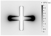
도 1을 다시 참조한다. 도 1에 도시된 바와 같이, 유전체창(18)의 대향면(18a) 상에는 도체 패턴(19)이 형성되어 있다. 도체 패턴(19)은, 슬롯판(36)의 각 슬롯(36a)으로부터 방사된 마이크로파에 따른 전계를 집중시킨다.Referring back to FIG. As shown in Fig. 1, a
여기서, 도체 패턴(19)과 슬롯판(36)의 각 슬롯(36a) 사이의 위치 관계에 대해서 설명한다. 도 3은 도체 패턴과 슬롯판의 각 슬롯 사이의 위치 관계의 일례를 설명하기 위한 도면이다. 또한, 도 3은 유전체창(18)의 대향면(18a)과는 반대측 면(18b) 상에 슬롯판(36)이 배치된 상태를 나타낸 평면도로서, 유전체창(18)을 대향면(18a) 측에서 본 평면도이다.Here, the positional relationship between the
도 3에 도시된 바와 같이, 도체 패턴(19)은, 유전체창(18)의 대향면(18a)에 있어서, 대향면(18a)에 수직인 방향에서 보았을 경우에 복수의 슬롯(36a)과 각각 겹치는 복수의 영역(18c)의 각각에 형성되어 있다.3, the
또한, 도 3의 예에서는, 도체 패턴(19)은, 복수의 영역(18c)의 각각에 형성되는 경우를 나타내었지만, 도체 패턴(19)은, 반드시 복수의 영역(18c)의 각각에 형성되지 않아도 좋다. 즉, 도체 패턴(19)은, 복수의 영역(18c) 중, 적어도 어느 하나의 영역(18c)에 형성되어도 좋다.3, the
도 4는 도 3에 도시된 도체 패턴 주위에 있어서의 전계 강도의 분포 시뮬레이션 결과의 일례를 나타낸 도면이다. 또한, 시뮬레이션에서는, 하나의 슬롯(36a)에 투입되는 마이크로파로서, 1 W의 마이크로파가 이용된 것으로 한다.4 is a diagram showing an example of the distribution simulation result of the electric field intensity around the conductor pattern shown in Fig. In the simulation, it is assumed that a microwave of 1 W is used as a microwave introduced into one
도 4의 시뮬레이션 결과로부터 밝혀진 바와 같이, 도 3에 도시된 도체 패턴(19) 주위의 전계 강도는, 5×10³(V/m) 이상이 되어, 미리 정해진 허용 스펙을 만족하는 것이었다. 즉, 유전체창(18)의 대향면(18a)에 있어서, 대향면(18a)에 수직인 방향에서 보았을 경우에 복수의 슬롯(36a)과 각각 겹치는 복수의 영역(18c)의 각각에 도체 패턴(19)을 형성함으로써, 각 슬롯(36a)으로부터 방사된 마이크로파에 따른 전계가 도체 패턴(19) 주위에 집중하는 것이 확인되었다.As evident from the simulation results of Fig. 4, the electric field strength around the
일 실시형태와 같이 유전체창(18)의 대향면(18a) 상에 도체 패턴(19)을 형성함으로써, 마이크로파에 따른 전계를 도체 패턴(19) 주위에 집중시킬 수 있다. 이 때문에, 일 실시형태에 따르면, 유전체창(18)의 대향면(18a)에 오목부 등을 형성하지 않고, 유전체창(18)의 대향면(18a)의 전계를 증대시킬 수 있다. 그 결과, 일 실시형태에 따르면, 유전체창(18)의 강도를 유지하면서 유전체창(18) 표면의 전계를 증대시킬 수 있어, 플라즈마를 효율적으로 생성할 수 있다.The electric field along the microwave can be concentrated around the
도 1을 다시 참조한다. 플라즈마 처리 장치(10)는, 이 장치에서 실시되는 플라즈마 프로세스에 이용하는 모든 처리 가스를 제공하는 처리 가스 공급부(80)를 구비하고, 처리 가스 공급부(80)로부터 제공되는 처리 가스를 챔버(12) 내에 도입하기 위한 가스 도입 기구로서, 3계통의 가스 라인, 즉 유전체창(18)에 가스 유로 및 가스 분출구를 설치하는 천장 가스 라인(제1 가스 도입부)(82)과, 상이한 높이 위치에서 챔버(12)의 측벽(12a)에 가스 유로 및 가스 분출구를 설치하는 하부 측벽 가스 라인(제2 가스 도입부)(84) 및 상부 측벽 가스 라인(제3 가스 도입부)(86)을 구비한다.Referring back to FIG. The
천장 가스 라인(82)은, 동축 도파관(16)의 내측 도체(16b)에, 그 안을 축 방향으로 관통하는 중공의 가스 유로(88)를 설치하고 있다. 내측 도체(16b)의 상단에 처리 가스 공급부(80)로부터의 제1 가스 공급관(90)이 접속되고, 제1 가스 공급관(90)과 동축 도파관(16)의 가스 유로(88)는 연통되어 있다. 제1 가스 공급관(90)에는 전자 밸브(개폐 밸브)(91)가 설치되어 있다.The
내측 도체(16b)의 하단에는 커넥터(92)가 접속되어 있다. 이 커넥터(92)는, 도체 예컨대 구리, 알루미늄, 스테인리스 혹은 이들의 합금으로 이루어지고, 유전체창(18)의 상면에 형성되어 있는 원통형의 오목부(18d)에 수용되어 있다. 커넥터(92)의 중심부에는, 동축 도파관(16)의 가스 유로(88)와 연통하는 관통 구멍 또는 가스 유로(92a)가 형성되어 있다.A
유전체창(18)의 하면(즉, 대향면(18a))의 중심부에는, 챔버(12) 내의 처리 공간(S)을 향하는 1개 또는 복수개의 천장 가스 분출구(94)가 형성되어 있다. 또한, 유전체창(18)의 중심부에는, 그 상면에 오목부(18d)의 바닥면 즉, 커넥터(92)의 가스 유로(92a)의 하단으로부터 천장 가스 분출구(94)로 통하는 가스 유로 즉, 유전체창 가스 유로(96)가 형성되어 있다. 유전체창 가스 유로(96) 및 천장 가스 분출구(94)가 인젝터를 구성한다.One or a plurality of ceiling
처리 가스 공급부(80)로부터 천장 가스 라인(82)으로 송출되는 처리 가스는, 제1 가스 공급관(90), 동축 도파관(16)의 가스 유로(88), 커넥터(92)의 가스 유로(92a) 및 유전체창 가스 유로(96)를 차례로 흘러, 종단의 천장 가스 분출구(94)로부터 스테이지(20)의 중심부를 향해 아래쪽으로 분사되도록 되어 있다.The process gas sent from the process
하부 측벽 가스 라인(84)은, 유전체창(18)과 스테이지(20)의 중간의 높이 위치에서 챔버(12)의 측벽(12a)의 내부에 환형으로 형성된 하부 버퍼실(매니폴드)(100)과, 주회(周回) 방향으로 등간격으로 하부 버퍼실(100)로부터 처리 공간(S)으로 향하는 다수(예컨대, 24개)의 하부 측벽 가스 분출구(102)와, 처리 가스 공급부(80)로부터 하부 버퍼실(100)까지 연장되는 제2 가스 공급관(104)을 갖고 있다. 제2 가스 공급관(104)에는 전자 밸브(개폐 밸브)(106)가 설치되어 있다.The lower
처리 가스 공급부(80)로부터 하부 측벽 가스 라인(84)으로 송출되는 처리 가스는, 제2 가스 공급관(104) 및 측벽(12a) 내부의 하부 버퍼실(100)을 차례로 흘러 종단의 하부 측벽 가스 분출구(102)로부터 스테이지(20)의 주변부를 향해 거의 수평 또는 비스듬하게 하향으로 분사되도록 되어 있다.The process gas delivered from the process
상부 측벽 가스 라인(86)은, 유전체창(18)에 가까운 높이 위치에서 챔버(12)의 측벽(12a)의 내부에 환형으로 형성된 상부 버퍼실(매니폴드)(108)과, 주회 방향으로 등간격으로 상부 버퍼실(108)로부터 처리 공간(S)을 향하는 다수(예컨대, 36개)의 상부 측벽 가스 분출구(110)와, 처리 가스 공급부(80)로부터 상부 버퍼실(108)까지 연장되는 제3 가스 공급관(112)을 갖고 있다. 제3 가스 공급관(112)에는 전자 밸브(114)가 설치되어 있다.The upper
처리 가스 공급부(80)로부터 상부 측벽 가스 라인(86)으로 송출되는 처리 가스는, 제3 가스 공급관(112) 및 측벽(12a) 내부의 상부 버퍼실(108)을 차례로 흘러, 종단의 상부 측벽 가스 분출구(110)로부터 유전체창(18)의 하면을 따라 거의 수평으로 분사되도록 되어 있다.The process gas delivered from the process
또한, 플라즈마 처리 장치(10)는, 상기와 같은 가스 도입 기구, 특히 천장 가스 라인(82)을 구비하는 구성과 함께 천장 가스 라인(82)의 제1 가스 공급관(90)과 배기부(55, 56)를 잇는 바이패스 배기 라인(116)을 구비하고 있다. 도시된 구성예에서는, 챔버(12)의 배기 구멍(12h)과 압력 조정기(55) 사이의 배기로(50)에 바이패스 배기 라인(116)의 출구(하단)를 접속하고 있다. 그러나, 압력 조정기(55)와 배기 장치(56) 사이의 배기로에 바이패스 배기 라인(116)의 출구를 접속하여도 좋다. 바이패스 배기 라인(116)에는 노멀 클로즈식의 전자 밸브(개폐 밸브)(118)가 설치된다. 또한, 천장 가스 라인(82)에 있어서 전자 밸브(91)의 하류측 내의 압력, 예컨대 제1 가스 공급관(90) 내의 압력을 계측하는 압력 센서(120)도 구비되어 있다.The
또한, 플라즈마 처리 장치(10)는, 플라즈마 처리 장치(10)의 각 구성 요소를 제어하기 위한 제어부(122)를 구비한다. 제어부(122)는, CPU(Central Processing Unit) 등의 제어 장치, 메모리 등의 기억 장치, 입출력 장치 등을 구비하는 컴퓨터여도 좋다. 제어부(122)는, 메모리에 기억된 제어 프로그램에 따라서 CPU가 동작함으로써, 플라즈마 처리 장치(10)의 각 구성 요소를 제어한다.The
제어부(122)는, 예컨대, 압력 조정기(55), 배기 장치(56), 고주파 전원(58), 매칭 유닛(60), 정전척(20b)용의 스위치(66), 마이크로파 발생기(14), 처리 가스 공급부(80), 각 가스 라인(82, 84, 86)의 전자 밸브(91, 106, 114), 바이패스 배기 라인(116)의 전자 밸브(118), 히터(HT∼HES), 전열 가스 공급부, 칠러 유닛 등의 개개의 동작 및 장치 전체의 동작을 제어한다. 또한, 제어부(122)는, 맨·머신·인터페이스용의 터치 패널(도시하지 않음) 및 이 플라즈마 처리 장치의 여러 동작을 규정하는 각종 프로그램이나 설정치 등의 데이터를 저장하는 기억 장치(도시하지 않음) 등과도 접속되어 있고, 각종 센서류로부터의 출력 신호, 특히 압력 센서(120)로부터의 출력 신호(압력 측정치 신호)(MSP)를 수취하도록 되어 있다.The
이와 같이 구성된 플라즈마 처리 장치(10)에서는, 인젝터를 통해 유전체창(18)의 천장 가스 분출구(94)로부터 처리 공간(S) 내로 처리 가스가 공급된다. 또한, 천장 가스 분출구(94)보다 아래쪽에 있어서, 하부 측벽 가스 분출구(102) 및 상부 측벽 가스 분출구(110)로부터 처리 가스가 공급된다. 또한, 안테나(15)로부터 유전체창(18)을 통해 처리 공간(S)으로 마이크로파가 도입된다. 이에 따라, 처리 공간(S)에 있어서 플라즈마가 발생한다.In the
다음에, 도체 패턴(19)의 형상에 대해서 설명한다. 도 5는 일 실시형태에 따른 도체 패턴의 확대 평면도이다. 도 5에 도시된 바와 같이, 도체 패턴(19)은, 십자형으로 형성된다. 다시 말하면, 도체 패턴(19)의 일부는, 직사각 형상으로 형성된다. 일 실시형태에서, 도체 패턴(19)은, 직사각 형상으로 형성된 제1 부분(19a)과, 직사각 형상으로 형성되고, 제1 부분(19a)에 교차하는 제2 부분(19b)을 갖는다. 일 실시형태에서는, 제1 부분(19a)의 길이(L1)와, 제2 부분(19b)의 길이(L2)는 동일하다.Next, the shape of the
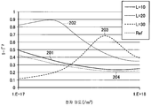
여기서, 도체 패턴(19)의 각 부분의 길이의 바람직한 범위에 대해서 설명한다. 도 6은 도체 패턴의 각 부분의 길이와, 플라즈마의 전자 밀도와, 플라즈마에 대한 마이크로파의 흡수 효율의 관계의 시뮬레이션 결과의 일례를 나타낸 도면이다. 도 6에 있어서, 횡축은, 처리 공간(S)에 있어서 발생한 플라즈마의 전자 밀도(/㎥)를 나타내고 있다. 또한, 도 6에 있어서, 종축은, 1-Γ2(Γ: 마이크로파의 반사 계수=반사파 전압/진행파 전압)를 나타내고 있다. 또한, 도 6에서는, 1-Γ2는 플라즈마에 대한 마이크로파의 흡수 효율로서, 1-Γ2의 값이 높을수록 플라즈마에 흡수되는 마이크로파의 전력이 큰 것을 나타내고 있다.Here, a preferable range of the length of each portion of the
또한, 도 6에 있어서, 그래프(201)는, 도체 패턴(19)의 제1 부분(19a)의 길이 및 제2 부분(19b)의 길이가 모두 10 ㎜인 경우의 마이크로파의 흡수 효율을 나타낸 그래프이다. 또한, 그래프(202)는, 도체 패턴(19)의 제1 부분(19a)의 길이 및 제2 부분(19b)의 길이가 모두 20 ㎜인 경우의 마이크로파의 흡수 효율을 나타낸 그래프이다. 또한, 그래프(203)는, 도체 패턴(19)의 제1 부분(19a)의 길이 및 제2 부분(19b)의 길이가 모두 30 ㎜인 경우의 마이크로파의 흡수 효율을 나타낸 그래프이다. 또한, 그래프(204)는, 유전체창(18)의 대향면(18a) 상에 도체 패턴(19)이 존재하지 않는 경우의 마이크로파의 흡수 효율을 나타낸 그래프이다.6, the
또한, 도 6에 도시된 시뮬레이션에 있어서의 유전체창(18)은, 알루미나에 의해 구성되는 것으로 한다.It should be noted that the
도 6에 도시된 바와 같이, 도체 패턴(19)의 제1 부분(19a)의 길이 및 제2 부분(19b)의 길이가 모두 20 ㎜인 경우, 마이크로파의 흡수 효율의 최대치가 가장 높아, 도체 패턴(19)의 제1 부분(19a)의 길이 및 제2 부분(19b)의 길이를 20 ㎜로부터 증가 또는 감소시킴으로써, 마이크로파의 흡수 효율의 최대치가 저하된다. 발명자는, 예의 검토를 더 거듭한 결과, 도체 패턴(19)의 제1 부분(19a)의 길이 및 제2 부분(19b)의 길이가 15 ㎜ 이상 25 ㎜ 이하의 범위 내인 경우, 마이크로파의 흡수 효율의 최대치가, 미리 정해진 허용 스펙 내에 유지되는 것을 알 수 있었다. 여기서, 유전체창(18)이 알루미나제인 경우, 유전체창(18)의 내부에서 전파되는 마이크로파의 파장이 40 ㎜이기 때문에, 유전체창(18)의 내부에서 전파되는 마이크로파의 파장의 1/2이 20 ㎜에 상당한다. 즉, 도 6의 시뮬레이션 결과로부터, 유전체창(18)의 내부에서 전파되는 마이크로파의 파장이 λ라고 하면, 도체 패턴(19)의 제1 부분(19a)의 길이 및 제2 부분(19b)의 길이가 3λ/8 이상 5λ/8 이하의 범위 내이면, 마이크로파의 흡수 효율의 최대치가, 미리 정해진 허용 스펙 내에 유지되는 것을 알 수 있었다. 따라서, 유전체창(18)의 내부에서 전파되는 마이크로파의 파장이 λ라고 하면, 도체 패턴(19)의 제1 부분(19a)의 길이 및 제2 부분(19b)의 길이는 3λ/8 이상 5λ/8 이하의 범위 내인 것이 바람직하다.6, when the length of the
또한, 도체 패턴(19)의 제1 부분(19a)의 길이 및 제2 부분(19b)의 길이는, 유전체창(18)의 내부에서 전파되는 마이크로파에 공진하는 길이인 것이 보다 바람직하다. 즉, 유전체창(18)의 내부에서 전파되는 마이크로파의 파장이 λ라고 하면, 도체 패턴(19)의 제1 부분(19a)의 길이 및 제2 부분(19b)의 길이는 λ/2인 것이 보다 바람직하다. 도체 패턴(19)과 마이크로파가 공진함으로써, 도체 패턴(19) 주위에 집중하는 전계가 증대되기 때문에, 마이크로파의 흡수 효율의 최대치를 더욱 향상시킬 수 있게 된다.It is more preferable that the length of the
이상 설명한 바와 같이, 일 실시형태의 플라즈마 처리 장치(10)에 따르면, 유전체창(18)의 대향면(18a) 상에 도체 패턴(19)을 형성함으로써, 마이크로파에 따른 전계를 도체 패턴(19) 주위에 집중시킬 수 있다. 이 때문에, 일 실시형태에 따르면, 유전체창(18)의 대향면(18a)에 오목부 등을 형성하지 않고, 유전체창(18)의 대향면(18a)의 전계를 증대시킬 수 있다. 그 결과, 일 실시형태에 따르면, 유전체창(18)의 강도를 유지하면서 유전체창(18) 표면의 전계를 증대시킬 수 있어, 플라즈마를 효율적으로 생성할 수 있다.As described above, according to the
또한, 상기 실시형태에 있어서, 도체 패턴(19)의 일부가 직사각 형상으로 형성되었으나, 도체 패턴(19)의 형상은 이것으로 한정되지 않는다. 이하, 도체 패턴(19)의 변형례에 대해서 설명한다.In the above embodiment, a part of the
도 7은 변형례 1에 따른 도체 패턴의 확대 평면도이다. 예컨대, 도 7에 도시된 바와 같이, 도체 패턴(19) 전체가 직사각 형상으로 형성되어도 좋다. 이 경우, 도체 패턴(19)의 길이(L3)는, 3λ/8 이상 5λ/8 이하의 범위 내인 것이 바람직하다.7 is an enlarged plan view of a conductor pattern according to
도 8은 도 7에 도시된 도체 패턴 주위에 있어서의 전계 강도의 분포의 시뮬레이션 결과의 일례를 나타낸 도면이다. 도 8의 시뮬레이션 결과로부터 밝혀진 바와 같이, 도 7에 도시된 도체 패턴(19) 주위의 전계 강도는, 5×10³(V/m) 이상이 되어, 미리 정해진 허용 스펙을 만족하는 것이었다. 즉, 도체 패턴(19) 전체가 직사각 형상으로 형성되는 경우라도, 마이크로파에 따른 전계가 도체 패턴(19) 주위에 집중하는 것이 확인되었다.8 is a diagram showing an example of the simulation result of the distribution of the electric field intensity around the conductor pattern shown in Fig. As evidenced by the simulation results in Fig. 8, the electric field intensity around the
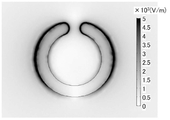
도 9는 변형례 2에 따른 도체 패턴의 확대 평면도이다. 예컨대, 도 9에 도시된 바와 같이, 도체 패턴(19) 전체가 C자 형상으로 형성되어도 좋다.Fig. 9 is an enlarged plan view of a conductor pattern according to
도 10은 도 9에 도시된 도체 패턴 주위에 있어서의 전계 강도의 분포의 시뮬레이션 결과의 일례를 나타낸 도면이다. 도 10의 시뮬레이션 결과로부터 밝혀진 바와 같이, 도 9에 도시된 도체 패턴(19) 주위의 전계 강도는, 5×10³(V/m) 이상이 되어, 미리 정해진 허용 스펙을 만족하는 것이었다. 즉, 도체 패턴(19) 전체가 직사각 형상으로 형성되는 경우라도, 마이크로파에 따른 전계가 도체 패턴(19) 주위에 집중하는 것이 확인되었다.10 is a diagram showing an example of the simulation result of the distribution of the electric field intensity around the conductor pattern shown in Fig. As evidenced by the simulation results of Fig. 10, the electric field strength around the
또한, 상기 실시형태에 있어서, 도체 패턴(19) 상에는 도체 패턴(19)을 플라즈마로부터 보호하기 위한 보호막이 형성되어도 좋다. 보호막으로는, 예컨대, 이트륨 함유 물질에 의한 막이 이용된다. 이트륨 함유 물질은, 예컨대, Y2O3 등이다.In the above embodiment, on the
10 : 플라즈마 처리 장치
12 : 챔버
14 : 마이크로파 발생기
15 : 안테나
18 : 유전체창
18a : 대향면
18b : 면
18c : 영역
19 : 도체 패턴
19a : 제1 부분
19b : 제2 부분
20 : 스테이지
36 : 슬롯판
36a : 슬롯10: plasma processing apparatus 12: chamber
14: microwave generator 15: antenna
18:
18b:
19:
19b: second part 20: stage
36:
Claims (6)
플라즈마 여기용의 마이크로파를 발생하는 마이크로파 발생기와,
상기 처리 공간에 대향하는 대향면을 갖는 유전체와,
상기 유전체의 상기 대향면과는 반대측 면 상에 설치되고, 상기 유전체를 통해 상기 마이크로파를 상기 처리 공간으로 방사하는 복수의 슬롯이 형성된 슬롯판과,
상기 유전체의 상기 대향면 상에 형성되고, 각 상기 슬롯으로부터 방사된 상기 마이크로파에 따른 전계를 집중시키는 도체 패턴
을 구비하는 것을 특징으로 하는 플라즈마 처리 장치.A processing vessel for partitioning the processing space,
A microwave generator for generating a microwave for plasma excitation,
A dielectric having an opposing surface facing the processing space;
A slot plate provided on a surface of the dielectric opposite to the facing surface and having a plurality of slots for radiating the microwave to the processing space through the dielectric,
A conductor pattern formed on the opposing face of the dielectric and concentrating an electric field along the microwave radiated from each of the slots;
And a plasma processing apparatus.
상기 도체 패턴은, 상기 유전체의 상기 대향면에 있어서, 상기 대향면에 수직인 방향에서 보았을 경우에 상기 복수의 슬롯과 각각 겹치는 복수의 영역 중, 적어도 어느 하나의 영역에 형성되는 것을 특징으로 하는 플라즈마 처리 장치.The method according to claim 1,
Wherein the conductor pattern is formed on at least any one of a plurality of regions overlapping with the plurality of slots when viewed in a direction perpendicular to the facing surface in the facing surface of the dielectric body Processing device.
상기 도체 패턴의 적어도 일부의 길이는, 상기 유전체의 내부에서 전파되는 상기 마이크로파의 파장이 λ라고 하면, 3λ/8 이상 5λ/8 이하의 범위 내인 것을 특징으로 하는 플라즈마 처리 장치.The semiconductor device according to claim 1, wherein at least a part of the conductor pattern is formed in a rectangular shape,
Wherein a length of at least a part of the conductor pattern is within a range of 3? / 8 to 5? / 8 when the wavelength of the microwave propagating inside the dielectric is?.
Applications Claiming Priority (2)
| Application Number | Priority Date | Filing Date | Title |
|---|---|---|---|
| JP2016028359A JP6695705B2 (en) | 2016-02-17 | 2016-02-17 | Plasma processing device |
| JPJP-P-2016-028359 | 2016-02-17 |
Publications (1)
| Publication Number | Publication Date |
|---|---|
| KR20170096960A true KR20170096960A (en) | 2017-08-25 |
Family
ID=59559759
Family Applications (1)
| Application Number | Title | Priority Date | Filing Date |
|---|---|---|---|
| KR1020170019956A KR20170096960A (en) | 2016-02-17 | 2017-02-14 | Plasma processing apparatus |
Country Status (3)
| Country | Link |
|---|---|
| US (1) | US10546725B2 (en) |
| JP (1) | JP6695705B2 (en) |
| KR (1) | KR20170096960A (en) |
Families Citing this family (7)
| Publication number | Priority date | Publication date | Assignee | Title |
|---|---|---|---|---|
| JP6804280B2 (en) * | 2016-12-07 | 2020-12-23 | 東京エレクトロン株式会社 | Plasma processing equipment and plasma processing method |
| JP7250376B2 (en) * | 2017-07-28 | 2023-04-03 | ヤマハファインテック株式会社 | Gas leak inspection system and gas leak inspection method |
| JP2022039820A (en) * | 2020-08-28 | 2022-03-10 | 東京エレクトロン株式会社 | Plasma treatment apparatus and plasma treatment method |
| KR20220107148A (en) * | 2021-01-21 | 2022-08-02 | 주식회사 히타치하이테크 | plasma processing unit |
| WO2023032725A1 (en) * | 2021-09-03 | 2023-03-09 | 東京エレクトロン株式会社 | Plasma processing device and plasma control method |
| JP2023180320A (en) * | 2022-06-09 | 2023-12-21 | 東京エレクトロン株式会社 | Plasma processing device and resonance frequency measurement method |
| CN115821215B (en) * | 2023-02-20 | 2023-04-28 | 成都富林达新材料有限公司 | Spraying device for suspension evaporation aluminum oxide |
Family Cites Families (6)
| Publication number | Priority date | Publication date | Assignee | Title |
|---|---|---|---|---|
| JP3164200B2 (en) * | 1995-06-15 | 2001-05-08 | 住友金属工業株式会社 | Microwave plasma processing equipment |
| JP5036092B2 (en) | 1999-03-24 | 2012-09-26 | 東京エレクトロン株式会社 | Microwave plasma processing equipment |
| JP3723783B2 (en) * | 2002-06-06 | 2005-12-07 | 東京エレクトロン株式会社 | Plasma processing equipment |
| US6998565B2 (en) * | 2003-01-30 | 2006-02-14 | Rohm Co., Ltd. | Plasma processing apparatus |
| US7998307B2 (en) * | 2006-09-12 | 2011-08-16 | Tokyo Electron Limited | Electron beam enhanced surface wave plasma source |
| JP6410622B2 (en) | 2014-03-11 | 2018-10-24 | 東京エレクトロン株式会社 | Plasma processing apparatus and film forming method |
-
2016
- 2016-02-17 JP JP2016028359A patent/JP6695705B2/en active Active
-
2017
- 2017-02-10 US US15/429,393 patent/US10546725B2/en active Active
- 2017-02-14 KR KR1020170019956A patent/KR20170096960A/en active Search and Examination
Also Published As
| Publication number | Publication date |
|---|---|
| JP6695705B2 (en) | 2020-05-20 |
| JP2017147129A (en) | 2017-08-24 |
| US10546725B2 (en) | 2020-01-28 |
| US20170236690A1 (en) | 2017-08-17 |
Similar Documents
| Publication | Publication Date | Title |
|---|---|---|
| KR20170096960A (en) | Plasma processing apparatus | |
| TWI681073B (en) | Plasma treatment device | |
| KR100494607B1 (en) | Plasma processing apparatus | |
| JP5082229B2 (en) | Plasma processing equipment | |
| EP0737256B1 (en) | Microwave plasma reactor | |
| KR101266890B1 (en) | Plasma processing device and plasma processing method | |
| KR100794806B1 (en) | Plasma processing apparatus and method, and slot antenna | |
| US5556475A (en) | Microwave plasma reactor | |
| KR20140106417A (en) | Plasma processing apparatus | |
| JPH09181052A (en) | Plasma treating apparatus | |
| US20090133838A1 (en) | Plasma Processor Apparatus | |
| KR20130114064A (en) | Plasma processing apparatus | |
| JP5723397B2 (en) | Plasma processing equipment | |
| JP5438260B2 (en) | Plasma processing equipment | |
| KR101274515B1 (en) | Plasma processing apparatus | |
| US9646867B2 (en) | Plasma processing apparatus, power supply unit and mounting table system | |
| TWI585813B (en) | Plasma processing device and plasma processing method | |
| KR101280567B1 (en) | Plasma processing apparatus | |
| JP5522887B2 (en) | Plasma processing equipment | |
| KR100984121B1 (en) | Apparatus for and method of treating substrate by plasma | |
| KR20060117237A (en) | Plasma processing apparatus and method | |
| KR102585041B1 (en) | plasma processing device | |
| KR102605240B1 (en) | Plasma processing device and plasma processing method | |
| KR20170093723A (en) | Plasama processing apparatus | |
| JPH09171900A (en) | Plasma generating device |
Legal Events
| Date | Code | Title | Description |
|---|---|---|---|
| A201 | Request for examination |