KR20170085286A - Memory system and operating method of memory system - Google Patents
Memory system and operating method of memory system Download PDFInfo
- Publication number
- KR20170085286A KR20170085286A KR1020160004725A KR20160004725A KR20170085286A KR 20170085286 A KR20170085286 A KR 20170085286A KR 1020160004725 A KR1020160004725 A KR 1020160004725A KR 20160004725 A KR20160004725 A KR 20160004725A KR 20170085286 A KR20170085286 A KR 20170085286A
- Authority
- KR
- South Korea
- Prior art keywords
- memory
- workload
- command
- read
- memory device
- Prior art date
Links
Images


Classifications
-
- G—PHYSICS
- G06—COMPUTING; CALCULATING OR COUNTING
- G06F—ELECTRIC DIGITAL DATA PROCESSING
- G06F12/00—Accessing, addressing or allocating within memory systems or architectures
- G06F12/02—Addressing or allocation; Relocation
- G06F12/0223—User address space allocation, e.g. contiguous or non contiguous base addressing
- G06F12/023—Free address space management
- G06F12/0238—Memory management in non-volatile memory, e.g. resistive RAM or ferroelectric memory
-
- G—PHYSICS
- G06—COMPUTING; CALCULATING OR COUNTING
- G06F—ELECTRIC DIGITAL DATA PROCESSING
- G06F3/00—Input arrangements for transferring data to be processed into a form capable of being handled by the computer; Output arrangements for transferring data from processing unit to output unit, e.g. interface arrangements
- G06F3/06—Digital input from, or digital output to, record carriers, e.g. RAID, emulated record carriers or networked record carriers
- G06F3/0601—Interfaces specially adapted for storage systems
- G06F3/0602—Interfaces specially adapted for storage systems specifically adapted to achieve a particular effect
- G06F3/061—Improving I/O performance
-
- G—PHYSICS
- G06—COMPUTING; CALCULATING OR COUNTING
- G06F—ELECTRIC DIGITAL DATA PROCESSING
- G06F12/00—Accessing, addressing or allocating within memory systems or architectures
- G06F12/02—Addressing or allocation; Relocation
- G06F12/06—Addressing a physical block of locations, e.g. base addressing, module addressing, memory dedication
- G06F12/0615—Address space extension
- G06F12/0623—Address space extension for memory modules
-
- G—PHYSICS
- G06—COMPUTING; CALCULATING OR COUNTING
- G06F—ELECTRIC DIGITAL DATA PROCESSING
- G06F13/00—Interconnection of, or transfer of information or other signals between, memories, input/output devices or central processing units
- G06F13/14—Handling requests for interconnection or transfer
- G06F13/16—Handling requests for interconnection or transfer for access to memory bus
- G06F13/1668—Details of memory controller
-
- G—PHYSICS
- G06—COMPUTING; CALCULATING OR COUNTING
- G06F—ELECTRIC DIGITAL DATA PROCESSING
- G06F3/00—Input arrangements for transferring data to be processed into a form capable of being handled by the computer; Output arrangements for transferring data from processing unit to output unit, e.g. interface arrangements
- G06F3/06—Digital input from, or digital output to, record carriers, e.g. RAID, emulated record carriers or networked record carriers
- G06F3/0601—Interfaces specially adapted for storage systems
- G06F3/0602—Interfaces specially adapted for storage systems specifically adapted to achieve a particular effect
- G06F3/0626—Reducing size or complexity of storage systems
-
- G—PHYSICS
- G06—COMPUTING; CALCULATING OR COUNTING
- G06F—ELECTRIC DIGITAL DATA PROCESSING
- G06F3/00—Input arrangements for transferring data to be processed into a form capable of being handled by the computer; Output arrangements for transferring data from processing unit to output unit, e.g. interface arrangements
- G06F3/06—Digital input from, or digital output to, record carriers, e.g. RAID, emulated record carriers or networked record carriers
- G06F3/0601—Interfaces specially adapted for storage systems
- G06F3/0628—Interfaces specially adapted for storage systems making use of a particular technique
- G06F3/0638—Organizing or formatting or addressing of data
- G06F3/064—Management of blocks
-
- G—PHYSICS
- G06—COMPUTING; CALCULATING OR COUNTING
- G06F—ELECTRIC DIGITAL DATA PROCESSING
- G06F3/00—Input arrangements for transferring data to be processed into a form capable of being handled by the computer; Output arrangements for transferring data from processing unit to output unit, e.g. interface arrangements
- G06F3/06—Digital input from, or digital output to, record carriers, e.g. RAID, emulated record carriers or networked record carriers
- G06F3/0601—Interfaces specially adapted for storage systems
- G06F3/0628—Interfaces specially adapted for storage systems making use of a particular technique
- G06F3/0655—Vertical data movement, i.e. input-output transfer; data movement between one or more hosts and one or more storage devices
- G06F3/0659—Command handling arrangements, e.g. command buffers, queues, command scheduling
-
- G—PHYSICS
- G06—COMPUTING; CALCULATING OR COUNTING
- G06F—ELECTRIC DIGITAL DATA PROCESSING
- G06F3/00—Input arrangements for transferring data to be processed into a form capable of being handled by the computer; Output arrangements for transferring data from processing unit to output unit, e.g. interface arrangements
- G06F3/06—Digital input from, or digital output to, record carriers, e.g. RAID, emulated record carriers or networked record carriers
- G06F3/0601—Interfaces specially adapted for storage systems
- G06F3/0668—Interfaces specially adapted for storage systems adopting a particular infrastructure
- G06F3/0671—In-line storage system
- G06F3/0673—Single storage device
- G06F3/0679—Non-volatile semiconductor memory device, e.g. flash memory, one time programmable memory [OTP]
-
- G—PHYSICS
- G11—INFORMATION STORAGE
- G11C—STATIC STORES
- G11C16/00—Erasable programmable read-only memories
- G11C16/02—Erasable programmable read-only memories electrically programmable
- G11C16/06—Auxiliary circuits, e.g. for writing into memory
- G11C16/10—Programming or data input circuits
-
- G—PHYSICS
- G11—INFORMATION STORAGE
- G11C—STATIC STORES
- G11C16/00—Erasable programmable read-only memories
- G11C16/02—Erasable programmable read-only memories electrically programmable
- G11C16/06—Auxiliary circuits, e.g. for writing into memory
- G11C16/26—Sensing or reading circuits; Data output circuits
Landscapes
- Engineering & Computer Science (AREA)
- Theoretical Computer Science (AREA)
- Physics & Mathematics (AREA)
- General Engineering & Computer Science (AREA)
- General Physics & Mathematics (AREA)
- Human Computer Interaction (AREA)
- Read Only Memory (AREA)
- Non-Volatile Memory (AREA)
- Semiconductor Memories (AREA)
Abstract
The present invention relates to a memory system for processing data in a memory device and a method of operating the memory system, including a plurality of pages including a plurality of memory cells connected to a plurality of word lines, A memory device including a plurality of memory blocks including the pages, a plurality of planes including the memory blocks, and a plurality of memory dies including the planes; And performing a command operation on the memory device corresponding to a command received from a host, calculating a command workload corresponding to the command, And a controller for calculating a memory workload of the command workload and dynamically scheduling the command operation corresponding to the command workload and the memory workload.

Description
BACKGROUND OF THE
Recently, a paradigm for a computer environment has been transformed into ubiquitous computing, which enables a computer system to be used whenever and wherever. As a result, the use of portable electronic devices such as mobile phones, digital cameras, and notebook computers is rapidly increasing. Such portable electronic devices typically use memory systems that use memory devices, i. E., Data storage devices. The data storage device is used as a main storage device or an auxiliary storage device of a portable electronic device.
The data storage device using the memory device is advantageous in that it has excellent stability and durability because there is no mechanical driving part, and the access speed of information is very fast and power consumption is low. As an example of a memory system having such advantages, a data storage device includes a USB (Universal Serial Bus) memory device, a memory card having various interfaces, a solid state drive (SSD), and the like.
Embodiments of the present invention provide a memory system and a method of operating a memory system that can minimize the complexity and performance degradation of a memory system and maximize utilization efficiency of the memory device to reliably process the data.
A memory system according to embodiments of the present invention includes a plurality of pages including a plurality of memory cells connected to a plurality of word lines and storing data, a plurality of memory blocks including the pages, A memory device including a plurality of planes including the memory blocks, and a plurality of memory dies including the planes; And performing a command operation on the memory device corresponding to a command received from a host, calculating a command workload corresponding to the command, And a controller for calculating a memory workload of the command workload and dynamically scheduling the command operation corresponding to the command workload and the memory workload.
Here, the controller can calculate a write command workload corresponding to a read command workload and a write command corresponding to a read command in the command have.
The controller may then calculate a read memory workload of the memory device for the read operation and a write memory workload of the memory device for the program operation in the command operation .
The controller may further calculate a background workload corresponding to a background operation that includes a copy or swap to the memory device.
The controller is further configured to determine a maximum lead for the memory device using the background workload and the read command workload and the write command workload using the parameters of the memory device for the read operation and the program operation, Memory workload and maximum write memory workload can be calculated.
The controller is further configured to dynamically adjust the throughput of the read operation and the throughput of the program operation using the maximum read memory workload and the maximum write memory workload and the read memory workload and the write memory workload You can decide.
The controller may also be configured to control the throughput of the read operation and the throughput of the program operation to a size or number of at least one of the memory dies, the planes, the memory blocks, You can decide.
Further, when receiving only the read command from the host, the controller determines the throughput of the read operation as the maximum read memory workload; When receiving only the write command from the host, the processing amount of the program operation can be determined as the maximum write memory workload.
The controller can dynamically adjust the throughput of the read operation and the throughput of the program operation in accordance with the read operation and the capability of the program operation of the memory device.
The controller may further include: a first calculation unit for calculating the read command workload and the write command workload; A second calculation unit for calculating the background workload; A monitoring unit monitoring the read operation and the program operation to calculate the read memory workload and the write memory workload; A calculation unit for calculating the maximum read memory workload and the maximum write memory workload; And a scheduling unit that dynamically determines a throughput of the read operation and a throughput of the program operation.
Here, the parameter may include a size and a time period of the memory device in which the read operation is performed, and a size and a time period of the memory device in which the program operation is performed.
A method of operating a memory system in accordance with embodiments of the present invention is a method for operating a plurality of pages each including a plurality of memory cells that are included in a plurality of memory blocks of a memory device and are connected to a plurality of word lines Receiving a command from a host; Calculating a command workload corresponding to the command and calculating a memory workload of the memory device in a command operation for the memory device corresponding to the command; Dynamically scheduling the command operation corresponding to the command workload and the memory workload; And performing the command operation between a controller of the memory device and the memory blocks included in a plurality of planes in a plurality of memory dies included in the memory device; . ≪ / RTI >
Wherein the calculating step calculates a write command workload corresponding to a read command workload and a write command corresponding to a read command in the command, ; And calculating a write memory workload of the memory device for a read memory workload and a program operation of the memory device for a read operation in the command operation .
The calculating step may further include calculating a background workload corresponding to a background operation including a copy or swap to the memory device. have.
And wherein said calculating step further comprises: using said memory device parameters for said read operation and said program operation, and said background workload and said read command workload and said write command workload, Calculating a maximum read memory workload and a maximum write memory workload.
In addition, the scheduling may comprise: using the maximum read memory workload and the maximum write memory workload, and the read memory workload and the write memory workload to calculate a throughput of the read operation and a throughput of the program operation, And dynamically determining the time required to perform the operation.
In addition, the determining may comprise: determining a throughput of the read operation and a throughput of the program operation based on a size of at least one of the memory dies, the planes, the memory blocks, And determining a number of the plurality of the plurality of the image data.
The determining step may include: determining a throughput of the read operation as the maximum read memory workload when receiving only the read command from the host; And determining the throughput of the program operation as the maximum write memory workload when receiving only the write command from the host.
The determining may further include dynamically adjusting the throughput of the read operation and the throughput of the program operation in accordance with the read operation and the capability of the program operation of the memory device can do.
Here, the parameter may include a size and a time period of the memory device in which the read operation is performed, and a size and a time period of the memory device in which the program operation is performed.
The memory system and the method of operating the memory system according to embodiments of the present invention minimize the complexity and performance degradation of the memory system and maximize the utilization efficiency of the memory device to quickly and reliably process the data.
1 schematically illustrates an example of a data processing system including a memory system in accordance with an embodiment of the present invention;
Figure 2 schematically illustrates an example of a memory device in a memory system according to an embodiment of the present invention;
3 schematically shows a memory cell array circuit of memory blocks in a memory device according to an embodiment of the present invention.
Figures 4-11 schematically illustrate a memory device structure in a memory system according to an embodiment of the present invention.
12 schematically illustrates an example of data processing operations in a memory device in a memory system according to an embodiment of the present invention.
13 schematically illustrates an operation of processing data in a memory system according to an embodiment of the present invention;
Hereinafter, preferred embodiments of the present invention will be described in detail with reference to the accompanying drawings. In the following description, only parts necessary for understanding the operation according to the present invention will be described, and the description of other parts will be omitted so as not to disturb the gist of the present invention.
Hereinafter, embodiments of the present invention will be described in more detail with reference to the drawings.
1 is a diagram schematically illustrating an example of a data processing system including a memory system according to an embodiment of the present invention.
Referring to FIG. 1, a
And, the
The
In addition, the storage devices implementing the
The
Here, the
The
As another example,
Meanwhile, the
The
More specifically, the
In addition, the
In addition, when reading data stored in the
Herein, the
The
The
The
The
The
The
Figure 2 schematically illustrates an example of a memory device in a memory system according to an embodiment of the present invention, Figure 3 schematically illustrates a memory cell array circuit of memory blocks in a memory device according to an embodiment of the present invention. And FIGS. 4 to 11 are views schematically showing a structure of a memory device in a memory system according to an embodiment of the present invention, and schematically the structure when the memory device is implemented as a three-dimensional nonvolatile memory device Fig.
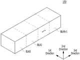
2, the
In addition, the
Each of the
3,
Here, FIG. 3 illustrates a
The
In addition, the read /
Referring to FIG. 4, the
Each memory block BLK may include a plurality of NAND strings NS extending along a second direction. A plurality of NAND strings NS may be provided along the first direction and the third direction. Each NAND string NS includes a bit line BL, at least one string select line SSL, at least one ground select line GSL, a plurality of word lines WL, at least one dummy word line DWL ), And a common source line (CSL). That is, each memory block includes a plurality of bit lines BL, a plurality of string select lines SSL, a plurality of ground select lines GSL, a plurality of word lines WL, a plurality of dummy word lines (DWL), and a plurality of common source lines (CSL).
5 and 6, an arbitrary memory block BLKi in the plurality of memory blocks of the
First, a
Then, on the
In a region on the
Are sequentially disposed along the first direction in the region on the
The
The insulating
In the region between the first doped region and the second
A conductive material extending along the first direction is provided between the insulating
In the region between the second doped region and the third
In the region between the third doped region and the fourth
On the
5 and 6, each of the
7, the insulating
The p-
The
The
The memory block BLKi may include a plurality of
Each NAND string NS may include a plurality of transistor structures TS disposed along a second direction. At least one of the plurality of transistor structures TS of each NAND string NS may operate as a string selection transistor (SST). At least one of the plurality of transistor structures TS of each NAND string NS may operate as a ground selection transistor (GST).
The gates (or control gates) may correspond to the
The
Second type doped
That is, the memory block BLKi includes a plurality of NAND strings NS extending in a direction perpendicular to the substrate 5111 (second direction), and a plurality of NAND strings NAND flash memory block (e.g., charge trapping type) to which the NAND flash memory is connected.
5 to 7,
5 to 7, three NAND strings NS are connected to one bit line BL. However, three NAND strings NS may be connected to one bit line BL, . For example, in the memory block BLKi, m NAND strings NS may be connected to one bit line BL. At this time, the number of conductive materials (5211 to 5291, 5212 to 5292, and 5213 to 5293) extending in the first direction by the number of NAND strings (NS) connected to one bit line (BL) The number of
5 to 7, three NAND strings NS are connected to one conductive material extending in the first direction. However, in the case where one conductive material extended in the first direction has three NAND strings NS are connected to each other. For example, n conductive n-strings NS may be connected to one conductive material extending in a first direction. At this time, the number of
8, in any block BLKi implemented with the first structure in the plurality of blocks of the
The string selection transistor SST of each NAND string NS may be connected to the corresponding bit line BL. The ground selection transistor GST of each NAND string NS can be connected to the common source line CSL. Memory cells MC may be provided between the string selection transistor SST and the ground selection transistor GST of each NAND string NS.
Hereinafter, for convenience of explanation, NAND strings NS may be defined in units of a row and a column, and NAND strings NS connected in common to one bit line may be defined as one column As will be described below. For example, the NAND strings NS11 to NS31 connected to the first bit line BL1 may correspond to the first column, and the NAND strings NS12 to NS32 connected to the second bit line BL2 may correspond to the second column And the NAND strings NS13 to NS33 connected to the third bit line BL3 may correspond to the third column. The NAND strings NS connected to one string select line (SSL) can form one row. For example, the NAND strings NS11 through NS13 connected to the first string selection line SSL1 may form a first row, the NAND strings NS21 through NS23 connected to the second string selection line SSL2, And the NAND strings NS31 to NS33 connected to the third string selection line SSL3 may form the third row.
Further, in each NAND string NS, a height can be defined. For example, in each NAND string NS, the height of the memory cell MC1 adjacent to the ground selection transistor GST is one. In each NAND string NS, the height of the memory cell may increase as the string selection transistor SST is adjacent to the string selection transistor SST. In each NAND string NS, the height of the memory cell MC7 adjacent to the string selection transistor SST is seven.
Then, the string selection transistors SST of the NAND strings NS in the same row can share the string selection line SSL. The string selection transistors SST of the NAND strings NS of the different rows can be connected to the different string selection lines SSL1, SSL2 and SSL3, respectively.
In addition, memory cells at the same height of the NAND strings NS in the same row can share the word line WL. That is, at the same height, the word lines WL connected to the memory cells MC of the NAND strings NS of different rows can be connected in common. The dummy memory cells DMC of the same height of the NAND strings NS in the same row can share the dummy word line DWL. That is, at the same height, the dummy word lines DWL connected to the dummy memory cells DMC of the NAND strings NS of the different rows can be connected in common.
For example, the word lines WL or the dummy word lines DWL may be connected in common in the layer provided with the
The common source line CSL may be connected in common to the NAND strings NS. For example, in the active region on the
That is, as shown in FIG. 8, the word lines WL of the same depth can be connected in common. Thus, when a particular word line WL is selected, all NAND strings NS connected to a particular word line WL can be selected. NAND strings NS in different rows may be connected to different string select lines SSL. Thus, by selecting the string selection lines SSL1 to SSL3, the NAND strings NS of unselected rows among the NAND strings NS connected to the same word line WL are selected from the bit lines BL1 to BL3 Can be separated. That is, by selecting the string selection lines SSL1 to SSL3, a row of NAND strings NS can be selected. Then, by selecting the bit lines BL1 to BL3, the NAND strings NS of the selected row can be selected in units of columns.
In each NAND string NS, a dummy memory cell DMC may be provided. The first to third memory cells MC1 to MC3 may be provided between the dummy memory cell DMC and the ground selection line GST.
The fourth to sixth memory cells MC4 to MC6 may be provided between the dummy memory cell DMC and the string selection line SST. Here, the memory cells MC of each NAND string NS can be divided into memory cell groups by the dummy memory cells DMC, and the memory cells MC of the divided memory cell groups adjacent to the ground selection transistor GST (For example, MC1 to MC3) may be referred to as a lower memory cell group, and memory cells (for example, MC4 to MC6) adjacent to the string selection transistor SST among the divided memory cell groups may be referred to as an upper memory cell Group. Hereinafter, with reference to FIGS. 9 to 11, the memory device according to the embodiment of the present invention will be described in more detail when the memory device is implemented as a three-dimensional nonvolatile memory device having a structure different from that of the first structure do.
9 and 10, an arbitrary memory block BLKj implemented in the second structure in the plurality of memory blocks of the
First, a
Then, on the
Further, fifth to eighth
In addition, a plurality of lower pillars penetrating the first to fourth
Each of the lower pillars DP and upper pillars UP includes an
The lower pillar DP and the upper pillar UP are connected via a pipe gate PG. The pipe gate PG may be disposed within the
On top of the lower pillar DP is provided a second type of
A
The first upper conductive material and the second upper
The first
And the first to fourth
That is, the lower string will include a source select transistor (SST), a first dummy memory cell (DMC1), and a first main memory cell and a second main memory cell (MMC1, MMC2). The upper string will include a third main memory cell and fourth main memory cells MMC3 and MMC4, a second dummy memory cell DMC2, and a drain select transistor DST.
9 and 10, the upper stream and the lower string may form a NAND string NS, and the NAND string NS may include a plurality of transistor structures TS. Here, the transistor structure included in the NAND stream in FIGS. 9 and 10 has been described in detail with reference to FIG. 7, and a detailed description thereof will be omitted here.
11, in an arbitrary block BLKj implemented in the second structure in the plurality of blocks of the
That is, in any block BLKj implemented with the second structure, the memory cells stacked along the first channel CH1, e.g., at least one source select gate and at least one drain select gate, And the memory cells stacked along the second channel CH2, such as at least one source select gate and at least one drain select gate, implement the second string ST2.
The first string ST1 and the second string ST2 are connected to the same drain select line DSL and the same source select line SSL and the first string ST1 is connected to the first bit line BL1 and the second string ST2 is connected to the second bit line BL2.
11, the case where the first string ST1 and the second string ST2 are connected to the same drain selection line DSL and the same source selection line SSL has been described as an example, , The first string ST1 and the second string ST2 are connected to the same source select line SSL and the same bit line BL so that the first string ST1 is connected to the first drain select line DSL1 And the second string ST2 is connected to the second drain select line DSL2 or the first string ST1 and the second string ST2 are connected to the same drain select line DSL and the same bit line BL The first string ST1 may be connected to the first source selection line SSL1 and the second string ST2 may be connected to the second source selection line SDSL2. 12 and 13, data processing to a memory device in a memory system according to an embodiment of the present invention, particularly a memory device corresponding to a command operation corresponding to a command received from the
12 schematically illustrates an example of a data processing operation in a memory device in a memory system according to an embodiment of the present invention. Hereinafter, for convenience of explanation, it is assumed that command data corresponding to a command received from the
In the following description, the
At this time, in the embodiment of the present invention, the throughput when the
Particularly, in the embodiment of the present invention, the read processing amount in the case of performing the read operation corresponding to the read command received from the
In the embodiment of the present invention, in consideration of a command workload including a read command workload and a write command workload, a memory workload including a lead memory workload and a write memory workload, and a background workload, Dynamically scheduling the read operation and the program operation corresponding to the read command and the write command received from the
In the embodiment of the present invention, the read command workload and the write command workload according to the read command and the write command received from the
12, the
The
Here,
More specifically, for example, the
Then, the
The
![]()
![]()
![]()
![]()
Equation (1) represents the execution rate of the program operation corresponding to the read command workload and the write command workload calculated by the size of the memory block, and Equation (2) represents the read command workload calculated by the number of commands and Represents the execution rate of the program operation corresponding to the write command workload. Equation (3) represents the execution rate of the read operation corresponding to the read command workload and the write command workload calculated by the size of the memory block, and Equation (4) represents the read command workload calculated by the number of commands and Indicates the execution rate of the read operation corresponding to the write command workload.
In addition, the
The

The
The
For example, the
In addition, the
In addition, when the
Thus, in the memory system according to the embodiment of the present invention, a command workload corresponding to the command received from the
13 is a diagram schematically illustrating an operation process of processing data in a memory system according to an embodiment of the present invention.
13, the memory system receives a command from the
Here, the memory system calculates the write command workload corresponding to the read command workload and the write command corresponding to the read command received from the
In
Then, in
Here, the calculation of the command workload, that is, the calculation of the read command work load and the write command work load, the read operation in the
While the invention has been shown and described with reference to certain preferred embodiments thereof, it will be understood by those skilled in the art that various changes and modifications may be made without departing from the spirit and scope of the invention. Therefore, the scope of the present invention should not be limited by the described embodiments, but should be determined by the scope of the appended claims, as well as the appended claims.
Claims (20)
The method comprising: performing a command operation on the memory device corresponding to a command received from a host; calculating a command workload corresponding to the command; A controller for calculating a memory workload and dynamically scheduling the command operation in response to the command workload and the memory workload.
Memory system.
Wherein the controller is operable to calculate a write command workload corresponding to a read command workload and a write command corresponding to a read command in the command,
Memory system.
Wherein the controller is operable to calculate a read memory workload of the memory device for a read operation in the command operation and a write memory workload of the memory device for program operation,
Memory system.
Wherein the controller is further adapted to calculate a background workload corresponding to a background operation including a copy or swap to the memory device,
Memory system.
Wherein the controller is operable to determine a maximum read memory workload for the memory device using the background workload and the read command workload and the write command workload for the memory device's parameters for the read operation and the program operation, Load and calculate the maximum light memory workload,
Memory system.
Wherein the controller dynamically determines a throughput of the read operation and a throughput of the program operation using the maximum read memory workload and the maximum write memory workload and the read memory workload and the write memory workload ,
Memory system.
The controller determines the throughput of the read operation and the throughput of the program operation as the size or number of at least one of the memory dies, the planes, the memory blocks, and the pages ,
Memory system.
The controller comprising:
Determining a throughput of the read operation as the maximum read memory workload when receiving only the read command from the host;
And determines the throughput of the program operation as the maximum write memory workload when receiving only the write command from the host.
Memory system.
Wherein the controller dynamically adjusts the throughput of the read operation and the throughput of the program operation in accordance with the read operation and the capability of the program operation of the memory device,
Memory system.
The controller comprising:
A first calculation unit for calculating the read command workload and the write command workload;
A second calculation unit for calculating the background workload;
A monitoring unit monitoring the read operation and the program operation to calculate the read memory workload and the write memory workload;
A calculation unit for calculating the maximum read memory workload and the maximum write memory workload; And
And a scheduling unit that dynamically determines a throughput of the read operation and a throughput of the program operation,
Memory system.
Wherein the parameter includes a size and a time period of the memory device in which the read operation is performed and a size and a time period of the memory device in which the program operation is performed,
Memory system.
Calculating a command workload corresponding to the command and calculating a memory workload of the memory device in a command operation for the memory device corresponding to the command;
Dynamically scheduling the command operation corresponding to the command workload and the memory workload; And
Performing the command operation between a controller of the memory device and the memory blocks included in a plurality of planes in a plurality of memory dies included in the memory device; Including,
A method of operating a memory system.
Wherein the calculating step comprises:
Calculating a write command workload corresponding to a read command workload and a write command corresponding to a read command in the command; And
And calculating a write memory workload of the memory device for a read memory workload and a program operation of the memory device for a read operation in the command operation.
A method of operating a memory system.
Wherein the calculating step comprises:
Further comprising computing a background workload corresponding to a background operation that includes a copy or swap to the memory device.
A method of operating a memory system.
Wherein the calculating step comprises:
Using the background workload and the read command workload and the write command workload to determine a maximum read memory workload and a maximum write workload for the memory device using parameters of the memory device for the read operation and the program operation, Further comprising: calculating a memory workload,
A method of operating a memory system.
Wherein the scheduling comprises:
And dynamically determining the throughput of the read operation and the throughput of the program operation using the maximum read memory workload and the maximum write memory workload and the read memory workload and the write memory workload doing,
A method of operating a memory system.
Wherein the determining comprises:
Determining the throughput of the read operation and the throughput of the program operation as a size or number of at least one of the memory dies, the planes, the memory blocks, and the pages doing,
A method of operating a memory system.
Wherein the determining comprises:
Determining a throughput of the read operation as the maximum read memory workload when receiving only the read command from the host; And
Further comprising: determining, when receiving only the write command from the host, the throughput of the program operation as the maximum write memory workload,
A method of operating a memory system.
Wherein the determining comprises:
Dynamically adjusting the throughput of the read operation and the throughput of the program operation in accordance with the read operation and the capability for the program operation of the memory device,
A method of operating a memory system.
Wherein the parameter includes a size and a time period of the memory device in which the read operation is performed and a size and a time period of the memory device in which the program operation is performed,
A method of operating a memory system.
Priority Applications (3)
| Application Number | Priority Date | Filing Date | Title |
|---|---|---|---|
| KR1020160004725A KR20170085286A (en) | 2016-01-14 | 2016-01-14 | Memory system and operating method of memory system |
| US15/192,761 US20170206007A1 (en) | 2016-01-14 | 2016-06-24 | Memory system and operating method of memory system |
| CN201610848672.7A CN107015760A (en) | 2016-01-14 | 2016-09-23 | The operating method of accumulator system and accumulator system |
Applications Claiming Priority (1)
| Application Number | Priority Date | Filing Date | Title |
|---|---|---|---|
| KR1020160004725A KR20170085286A (en) | 2016-01-14 | 2016-01-14 | Memory system and operating method of memory system |
Publications (1)
| Publication Number | Publication Date |
|---|---|
| KR20170085286A true KR20170085286A (en) | 2017-07-24 |
Family
ID=59315091
Family Applications (1)
| Application Number | Title | Priority Date | Filing Date |
|---|---|---|---|
| KR1020160004725A KR20170085286A (en) | 2016-01-14 | 2016-01-14 | Memory system and operating method of memory system |
Country Status (3)
| Country | Link |
|---|---|
| US (1) | US20170206007A1 (en) |
| KR (1) | KR20170085286A (en) |
| CN (1) | CN107015760A (en) |
Cited By (4)
| Publication number | Priority date | Publication date | Assignee | Title |
|---|---|---|---|---|
| WO2019147490A1 (en) * | 2018-01-23 | 2019-08-01 | Micron Technology, Inc. | Identifying a read operation for a storage device based on a workload of a host system |
| CN111104062A (en) * | 2019-11-22 | 2020-05-05 | 中科寒武纪科技股份有限公司 | Storage management method, device and storage medium |
| KR20200073592A (en) * | 2018-12-14 | 2020-06-24 | 에스케이하이닉스 주식회사 | Memory controller and memory system having the same |
| US11461177B2 (en) | 2020-03-06 | 2022-10-04 | SK Hynix Inc. | Data storage device and method of operating the same |
Families Citing this family (12)
| Publication number | Priority date | Publication date | Assignee | Title |
|---|---|---|---|---|
| KR20190023247A (en) * | 2017-08-28 | 2019-03-08 | 에스케이하이닉스 주식회사 | Memory system and operation method thereof |
| US10747441B2 (en) * | 2017-08-30 | 2020-08-18 | Micron Technology, Inc. | Efficient allocation of storage connection resources |
| KR20190026231A (en) * | 2017-09-04 | 2019-03-13 | 에스케이하이닉스 주식회사 | Memory system and operating method of memory system |
| KR102419895B1 (en) | 2018-02-09 | 2022-07-12 | 삼성전자주식회사 | Non-volatile memory device and read method thereof |
| US11295818B2 (en) | 2018-02-09 | 2022-04-05 | Samsung Electronics Co., Ltd. | Non-volatile memory device, operating method thereof, and storage device having the same |
| CN108595367B (en) * | 2018-04-25 | 2021-12-10 | 广州高专资讯科技有限公司 | Server system based on computer cluster in local area network |
| KR20200016074A (en) * | 2018-08-06 | 2020-02-14 | 에스케이하이닉스 주식회사 | Data processing system and operating method thereof |
| CN113126883B (en) * | 2019-12-30 | 2024-07-09 | 深圳Tcl新技术有限公司 | Data processing method, system and storage medium |
| US11422616B2 (en) * | 2020-03-26 | 2022-08-23 | Intel Corporation | System, apparatus and method for dynamically adjusting platform power and performance based on task characteristics |
| KR20220087785A (en) | 2020-12-18 | 2022-06-27 | 에스케이하이닉스 주식회사 | Memory controller and storage device including same |
| KR20220087782A (en) * | 2020-12-18 | 2022-06-27 | 에스케이하이닉스 주식회사 | Memory controller and storage device including same |
| KR20220165980A (en) * | 2021-06-09 | 2022-12-16 | 에스케이하이닉스 주식회사 | Controller and operation method thereof |
Family Cites Families (5)
| Publication number | Priority date | Publication date | Assignee | Title |
|---|---|---|---|---|
| CN1258713C (en) * | 2003-11-14 | 2006-06-07 | 清华大学 | Data distribution dynamic mapping method based on magnetic disc characteristic |
| US20070143561A1 (en) * | 2005-12-21 | 2007-06-21 | Gorobets Sergey A | Methods for adaptive file data handling in non-volatile memories with a directly mapped file storage system |
| US20120110239A1 (en) * | 2010-10-27 | 2012-05-03 | Seagate Technology Llc | Causing Related Data to be Written Together to Non-Volatile, Solid State Memory |
| US9519428B2 (en) * | 2012-09-26 | 2016-12-13 | Qualcomm Incorporated | Dynamically improving performance of a host memory controller and a memory device |
| CN105117285B (en) * | 2015-09-09 | 2019-03-19 | 重庆大学 | A kind of nonvolatile memory method for optimizing scheduling based on mobile virtual system |
-
2016
- 2016-01-14 KR KR1020160004725A patent/KR20170085286A/en unknown
- 2016-06-24 US US15/192,761 patent/US20170206007A1/en not_active Abandoned
- 2016-09-23 CN CN201610848672.7A patent/CN107015760A/en active Pending
Cited By (5)
| Publication number | Priority date | Publication date | Assignee | Title |
|---|---|---|---|---|
| WO2019147490A1 (en) * | 2018-01-23 | 2019-08-01 | Micron Technology, Inc. | Identifying a read operation for a storage device based on a workload of a host system |
| KR20200073592A (en) * | 2018-12-14 | 2020-06-24 | 에스케이하이닉스 주식회사 | Memory controller and memory system having the same |
| US11086528B2 (en) | 2018-12-14 | 2021-08-10 | SK Hynix Inc. | Memory controller and memory system having the same |
| CN111104062A (en) * | 2019-11-22 | 2020-05-05 | 中科寒武纪科技股份有限公司 | Storage management method, device and storage medium |
| US11461177B2 (en) | 2020-03-06 | 2022-10-04 | SK Hynix Inc. | Data storage device and method of operating the same |
Also Published As
| Publication number | Publication date |
|---|---|
| CN107015760A (en) | 2017-08-04 |
| US20170206007A1 (en) | 2017-07-20 |
Similar Documents
| Publication | Publication Date | Title |
|---|---|---|
| KR102534633B1 (en) | Memory system and operating method of memory system | |
| KR20170085286A (en) | Memory system and operating method of memory system | |
| KR20170061221A (en) | Memory system and operating method of memory system | |
| KR102514388B1 (en) | Memory system and operating method of memory system | |
| KR20160127524A (en) | Memory system and operating method of memory system | |
| KR20160112135A (en) | Memory system and operating method of memory system | |
| KR20160073873A (en) | Memory system and operating method of memory system | |
| KR20170075855A (en) | Memory system and operating method of memory system | |
| KR20170050953A (en) | Memory system and operation method for the same | |
| KR102310580B1 (en) | Memory system and operating method of memory system | |
| KR20160075166A (en) | Data processing system and operating method of data processing system | |
| KR20160148952A (en) | Memory system and operating method of memory system | |
| KR20160058458A (en) | Memory system and operating method of memory system | |
| KR20160032910A (en) | Memory system and operating method of memory system | |
| KR20170059049A (en) | Memory system and operating method of memory system | |
| KR20170060206A (en) | Memory system and operating method of memory system | |
| KR20170057902A (en) | Memory system and operating method of memory system | |
| KR20170084460A (en) | Memory system and operating method of memory system | |
| KR20170073792A (en) | Memory system and operating method of memory system | |
| KR20170076878A (en) | Memory system and operating method of memory system | |
| KR20170061218A (en) | Memory system and operating method of memory system | |
| KR20160075165A (en) | Memory system and operating method of memory system | |
| KR20170078310A (en) | Memory system and operation methode for the same | |
| KR20170118284A (en) | Memory system and operating method of memory system | |
| KR20170078315A (en) | Memory system and operation method for the same |