KR20170072018A - Biological information measurement device using sensor array - Google Patents
Biological information measurement device using sensor array Download PDFInfo
- Publication number
- KR20170072018A KR20170072018A KR1020150180337A KR20150180337A KR20170072018A KR 20170072018 A KR20170072018 A KR 20170072018A KR 1020150180337 A KR1020150180337 A KR 1020150180337A KR 20150180337 A KR20150180337 A KR 20150180337A KR 20170072018 A KR20170072018 A KR 20170072018A
- Authority
- KR
- South Korea
- Prior art keywords
- sensor array
- biometric information
- photoreactive
- sensor
- average value
- Prior art date
Links
Images


Classifications
-
- A—HUMAN NECESSITIES
- A61—MEDICAL OR VETERINARY SCIENCE; HYGIENE
- A61B—DIAGNOSIS; SURGERY; IDENTIFICATION
- A61B5/00—Measuring for diagnostic purposes; Identification of persons
- A61B5/0059—Measuring for diagnostic purposes; Identification of persons using light, e.g. diagnosis by transillumination, diascopy, fluorescence
-
- A—HUMAN NECESSITIES
- A61—MEDICAL OR VETERINARY SCIENCE; HYGIENE
- A61B—DIAGNOSIS; SURGERY; IDENTIFICATION
- A61B5/00—Measuring for diagnostic purposes; Identification of persons
- A61B5/0002—Remote monitoring of patients using telemetry, e.g. transmission of vital signals via a communication network
-
- A—HUMAN NECESSITIES
- A61—MEDICAL OR VETERINARY SCIENCE; HYGIENE
- A61B—DIAGNOSIS; SURGERY; IDENTIFICATION
- A61B5/00—Measuring for diagnostic purposes; Identification of persons
- A61B5/02—Detecting, measuring or recording pulse, heart rate, blood pressure or blood flow; Combined pulse/heart-rate/blood pressure determination; Evaluating a cardiovascular condition not otherwise provided for, e.g. using combinations of techniques provided for in this group with electrocardiography or electroauscultation; Heart catheters for measuring blood pressure
- A61B5/024—Detecting, measuring or recording pulse rate or heart rate
-
- A—HUMAN NECESSITIES
- A61—MEDICAL OR VETERINARY SCIENCE; HYGIENE
- A61B—DIAGNOSIS; SURGERY; IDENTIFICATION
- A61B5/00—Measuring for diagnostic purposes; Identification of persons
- A61B5/145—Measuring characteristics of blood in vivo, e.g. gas concentration, pH value; Measuring characteristics of body fluids or tissues, e.g. interstitial fluid, cerebral tissue
- A61B5/1455—Measuring characteristics of blood in vivo, e.g. gas concentration, pH value; Measuring characteristics of body fluids or tissues, e.g. interstitial fluid, cerebral tissue using optical sensors, e.g. spectral photometrical oximeters
- A61B5/14551—Measuring characteristics of blood in vivo, e.g. gas concentration, pH value; Measuring characteristics of body fluids or tissues, e.g. interstitial fluid, cerebral tissue using optical sensors, e.g. spectral photometrical oximeters for measuring blood gases
-
- A—HUMAN NECESSITIES
- A61—MEDICAL OR VETERINARY SCIENCE; HYGIENE
- A61B—DIAGNOSIS; SURGERY; IDENTIFICATION
- A61B5/00—Measuring for diagnostic purposes; Identification of persons
- A61B5/68—Arrangements of detecting, measuring or recording means, e.g. sensors, in relation to patient
- A61B5/6801—Arrangements of detecting, measuring or recording means, e.g. sensors, in relation to patient specially adapted to be attached to or worn on the body surface
- A61B5/6813—Specially adapted to be attached to a specific body part
-
- A—HUMAN NECESSITIES
- A61—MEDICAL OR VETERINARY SCIENCE; HYGIENE
- A61B—DIAGNOSIS; SURGERY; IDENTIFICATION
- A61B5/00—Measuring for diagnostic purposes; Identification of persons
- A61B5/72—Signal processing specially adapted for physiological signals or for diagnostic purposes
- A61B5/7225—Details of analog processing, e.g. isolation amplifier, gain or sensitivity adjustment, filtering, baseline or drift compensation
-
- A—HUMAN NECESSITIES
- A61—MEDICAL OR VETERINARY SCIENCE; HYGIENE
- A61B—DIAGNOSIS; SURGERY; IDENTIFICATION
- A61B5/00—Measuring for diagnostic purposes; Identification of persons
- A61B5/72—Signal processing specially adapted for physiological signals or for diagnostic purposes
- A61B5/7235—Details of waveform analysis
Landscapes
- Health & Medical Sciences (AREA)
- Life Sciences & Earth Sciences (AREA)
- Engineering & Computer Science (AREA)
- Physics & Mathematics (AREA)
- Surgery (AREA)
- Public Health (AREA)
- Pathology (AREA)
- Veterinary Medicine (AREA)
- Biomedical Technology (AREA)
- Heart & Thoracic Surgery (AREA)
- Medical Informatics (AREA)
- Molecular Biology (AREA)
- Biophysics (AREA)
- Animal Behavior & Ethology (AREA)
- General Health & Medical Sciences (AREA)
- Physiology (AREA)
- Signal Processing (AREA)
- Artificial Intelligence (AREA)
- Computer Vision & Pattern Recognition (AREA)
- Psychiatry (AREA)
- Cardiology (AREA)
- Spectroscopy & Molecular Physics (AREA)
- Optics & Photonics (AREA)
- Computer Networks & Wireless Communication (AREA)
- Power Engineering (AREA)
- Measurement Of The Respiration, Hearing Ability, Form, And Blood Characteristics Of Living Organisms (AREA)
Abstract
A sensor array including a plurality of photoreactive sensors amplifying photoreactivity of light reflected or transmitted from the skin tissue and outputting absorption information associated with tissue activity and function of the skin tissue with respect to the amplified light; And a sensor array for measuring an average value of the biometric information with respect to the sensor array based on the absorbed information.

Description
The present invention relates to an apparatus for measuring bio-information using a sensor array, and more particularly, to a bio-information measuring apparatus using a sensor array, which uses an absorption information output from a sensor array including a plurality of photoreactive sensors for amplifying photoreactivity, The present invention relates to a biometric information measuring apparatus using a sensor array for measuring a value.
Oxygen saturation refers to the percentage of erythrocytes in which hemoglobin and oxygen are actually bound, expressed as a percentage (%). The normal range of oxygen saturation is 97 to 100%, and if it is less than 90%, hypoxia is suspected.
Conventional oxygen saturation testing methods for preventing or treating diseases related to oxygen saturation include invasive methods such as Arterial Blood Gas Analysis (ABGA) and non-invasive pulse oximeter tests, Pulse oximetry, an invasive test method, has been preferred.
The principle of pulse oximeter to measure heart rate and oxygen saturation is to measure pulses in arterial and capillary blood vessels from pulse waves (pulse waves accompanied by heart beat) that are made by changes in blood volume and to measure oxygenated hemoglobin (O 2 Hb) and reduced hemoglobin (hemoglobin separated from oxygen) by measuring the oxygen saturation (SpO 2 ).
Conventional pulse oximeter techniques employing the principle of measurement of pulse oximeter were mainly used as a finger pulse oximeter and a chest strap heart rate monitor.
Conventional Finger Pulse Oximeter is a device for percutaneous measurement of blood oxygen saturation using light detection by a probe worn on the finger of a user (patient). It is a device that detects the wave form produced by the pulsating blood, The pulse is measured at a cycle indicated by a blood volume fluctuation waveform.
In addition, the conventional chest strap heart rate monitor is an optical measurement method using an electrode included in a strap surrounding a chest, and measures a pulse at a cycle represented by a waveform generated by a reflected light source in a heart region.
However, the conventional finger pulse oximeter is difficult to be worn continuously by the finger measurement method. There is a limitation in monitoring when the baby is worn, there is a limit to the measurement of the heartbeat and oxygen saturation for the exercise intensity, There was a problem.
In addition, the conventional chest strap heart rate monitor can be continuously worn, but it can be continuously monitored due to the inconvenience of the wearing feeling and cumbersome usage method. However, there is a feeling of heterogeneity of wearing, .
In order to overcome the problems of the prior art, a pulse oximeter technique for measuring oxygen saturation and heart rate by attaching to the body has been developed. However, in the conventional pulse oximeter technique, a single sensor is used to measure the oxygen saturation and heart rate of the body, There is a limitation that only a certain portion (area) of the body corresponding to the size (area) of a single sensor can be measured, and a problem that the measurement value of the biometric information including oxygen saturation and heartbeat varies depending on the attachment position or area of the body .
In addition, the conventional pulse oximeter technique has a problem in that it is impossible to measure the temperature of various parts of the body, and there is a limit that can not be accurately measured to the first digit of oxygen saturation and heartbeat, There is a limit to the reliability of
The present invention relates to a biometric information measuring apparatus using a sensor array capable of measuring biometric information including heartbeat and oxygen saturation for skin tissue in a non-invasive manner in a short time by sensing the reflectivity or transmittance of light reflected from the skin tissue .
In addition, the present invention measures the absorption information of the skin tissue accurately with respect to the part to be measured by the user using the body-attached bio-information measuring device which is flexible and has good biocompatibility and does not slip on the skin, And to provide a biometric information measuring device using a sensor array capable of transmitting an average value of the measured biometric information to the outside and treating and preventing the biometric information in real time.
The present invention also relates to a photoconductor which uses a transition metal chalcogenide compound as a material of a channel region and amplifies photoconductivity through a local gate electrode and a non-overlap region operating as a photoconductor in a non-overlapping channel region, And a photoreactive sensor including an optical amplification phototransistor to which a transistor is coupled.
In addition, the present invention provides a sensor array that includes a plurality of photoreactive sensors and is manufactured in the form of a patch. The sensor array can measure an accurate oxygen saturation and a heartbeat (pulse) with respect to a contact area of a skin tissue Information measuring apparatus.
In addition, the present invention measures the wide contact area of skin tissue to be measured based on a plurality of photoreactive sensors, the average value of oxygen saturation and heartbeat of various tissues with respect to various parts, A bio-information measuring device using a sensor array capable of reducing an error to the bio-information measuring device.
A biometric information measuring apparatus using a sensor array according to an embodiment of the present invention includes a light source unit for generating light and a switching thin film transistor connected to the light source unit for amplifying optical reactivity of light generated from the light source unit, And a plurality of photoreactive sensors for outputting absorption information for mapping biometric information related to tissue activity and function of the skin tissue with respect to amplified light having reactivity, And an average value measuring unit for measuring an average value of the biometric information for the sensor array based on the absorption information output from the photoreactive sensor.
The photoreactive sensor according to one embodiment may include one or more optical amplification phototransistors arranged in an active matrix form.
The optical amplification phototransistor according to an embodiment includes a channel region formed between a local gate electrode, a source electrode, a drain electrode, and the source electrode and the drain electrode, and includes a non-overlap region that is not overlapped with the gate electrode Channel region, and the non-overlap region may operate as a photo conductor that amplifies photoconductivity.
The non-overlap region may be formed in both lateral directions of the source electrode and the drain electrode, or may be formed in one of the lateral direction of the source electrode and the drain electrode.
The channel region according to an exemplary embodiment may be formed of a transition metal chalcogenide compound.
The biometric information according to one embodiment may be associated with tissue activity and function associated with at least one of heart rate and oxygen saturation.
The sensor array according to an embodiment may be formed in a patch-like structure by being connected to an IC circuit formed on the substrate.
The substrate according to an exemplary embodiment may be formed of at least one of paper, polymer, woven fabric, and metal foil.
The apparatus for measuring bio-information using a sensor array according to an embodiment of the present invention includes a communication module for transmitting an average value of the measured biometric information to the outside, and a control module for controlling the plurality of photoreactive sensors And a controller for controlling the average value measuring unit to measure the average value of the biometric information based on the absorption information measured by the at least one photoreactive sensor selected from among the photoreactive sensors.
According to the embodiment of the present invention, biometrics information including heart rate and oxygen saturation for skin tissue can be measured in real time in a non-invasively short time by sensing the reflectance or transmittance of light reflected from the skin tissue.
According to the embodiment of the present invention, absorption information of the skin tissue is accurately measured on a site to be measured by a user using a body-attached bio-information measuring device which is flexible and has good biocompatibility and does not slip on the skin, The average value of the measured biometric information is transmitted to the outside based on the absorption information, and treatment and prevention according to the biometric information can be performed in real time.
Further, according to an embodiment of the present invention, there is also provided a method of manufacturing a semiconductor device, which uses a transition metal chalcogenide compound as a material of a channel region and amplifies photoconductivity through a non-overlap region operating with a local gate electrode and a non- A photoconductor, and a photoreactive sensor including an optical amplification phototransistor coupled with a phototransistor.
Also, according to the embodiment of the present invention, a sensor array including a plurality of photoreactive sensors can be manufactured in a patch shape, and accurate oxygen saturation and heart rate (pulse) can be measured with respect to the contact area of the skin tissue .
According to an embodiment of the present invention, a wide contact area of skin tissue to be measured based on a plurality of photoreactive sensors, an average value of oxygen saturation and heartbeat of various tissues with respect to various parts are measured, It is possible to reduce errors in different absorption information.
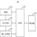
FIG. 1 illustrates an embodiment of a biometric information measuring apparatus using a sensor array according to an embodiment of the present invention.
FIG. 2 is a block diagram illustrating a configuration of a biometric information measuring apparatus using a sensor array according to an embodiment of the present invention. Referring to FIG.
FIG. 3 illustrates a detailed configuration of a sensor array according to an embodiment of the present invention.
4 illustrates a structure and a circuit diagram of a photoreactive sensor-based sensor array according to an embodiment of the present invention.
5 is a graph showing average values measured through a sensor array including a photoreactive sensor according to an embodiment of the present invention.
6 illustrates an optical amplification phototransistor of a photoreactive sensor according to an embodiment of the present invention.
7 is a circuit block diagram of an optical amplification phototransistor of a photoreactive sensor according to an embodiment of the present invention.
8 is a graph showing characteristics of a photoconductor of an optical amplification phototransistor according to an embodiment of the present invention.
9 is a transfer curve graph of an optical amplification phototransistor according to an embodiment of the present invention.
Figure 10 shows a graph of photoreactive properties.
11 illustrates the sensitivity of the optical amplification phototransistor according to the non-overlap length according to the embodiment of the present invention.
Hereinafter, embodiments of the present invention will be described in detail with reference to the accompanying drawings and accompanying drawings, but the present invention is not limited to or limited by the embodiments.
The terminology used herein is for the purpose of illustrating embodiments and is not intended to be limiting of the present invention. In the present specification, the singular form includes plural forms unless otherwise specified in the specification. It is noted that the terms "comprises" and / or "comprising" used in the specification are intended to be inclusive in a manner similar to the components, steps, operations, and / Or additions.
As used herein, the terms " an embodiment, " " an embodiment, a side, " " an example ", and the like, are not necessarily to be construed as advantageous or advantageous over other aspects or designs .
Also, the term 'or' implies an inclusive or 'inclusive' rather than an exclusive or 'exclusive'. That is, unless expressly stated otherwise or clear from the context, the expression 'x uses a or b' means any of the natural inclusive permutations.
Also, the phrase "a" or "an ", as used in the specification and claims, unless the context clearly dictates otherwise, or to the singular form, .
Furthermore, the terms first, second, etc. used in the specification and claims may be used to describe various elements, but the elements should not be limited by the terms. The terms are used only for the purpose of distinguishing one component from another.
Unless defined otherwise, all terms (including technical and scientific terms) used herein may be used in a sense commonly understood by one of ordinary skill in the art to which this invention belongs. Also, commonly used predefined terms are not ideally or excessively interpreted unless explicitly defined otherwise.
In the following description of the present invention, a detailed description of known functions and configurations incorporated herein will be omitted when it may make the subject matter of the present invention rather unclear. The terminology used herein is a term used for appropriately expressing an embodiment of the present invention, which may vary depending on the user, the intent of the operator, or the practice of the field to which the present invention belongs. Therefore, the definitions of these terms should be based on the contents throughout this specification.
FIG. 1 illustrates an embodiment of a biometric information measuring apparatus using a sensor array according to an embodiment of the present invention.
Referring to FIG. 1, an
The
A biometric
The light source unit may generate a light source, and the average value measuring unit may measure an average value of the biometric information with respect to the
In addition, the communication module may transmit the average value of the measured biometric information to the outside, and the control unit may control to measure an average value of the biometric information, and the power supply unit may include a light source unit, an average value measurement unit, The control unit can supply at least one of the driving power.
1, an
The terminal 200 may transmit information on heart rate and oxygen saturation to the user (patient) based on at least one of the absorption information and the average value of the biometric information received from the living body
For example, the terminal 200 may receive at least one of the absorption information and the average value of the biometric information received from the biometric
Also, the terminal 200 may control the
For example, the terminal 200 may transmit a control command (e.g., a pulse) to the
In addition, the terminal 200 can control to select any photoreactive sensor according to a part of the body to be measured out of a plurality of photoreactive sensors, and to control the sensor array including the photoreactive sensor with a control command (a) .
According to an embodiment, the terminal 200 may be at least one of a terminal, a smart phone, a tablet PC, and a PC carried by the user, but is not limited thereto.
Also, the terminal 200 may transmit at least one of the absorption information and the average value of the biometric information received from the biometric
The integration server manages at least any one of the absorption information and the average value of the biometric information received from the terminal 200, analyzes the change of the user's data and health state, and transmits the analysis to the terminal 200.
In addition, the integration server can provide the user's data to healthcare professionals, hospitals, health centers, and specialists for healthcare guidance. Based on the analyzed data, the user can select the appropriate exercise, food, lifestyle and prescription Or at least one of them may be provided.
Also, according to the embodiment, the configuration of the integrated server may be performed in the terminal 200 as well.
FIG. 2 is a block diagram illustrating a configuration of a biometric information measuring apparatus using a sensor array according to an embodiment of the present invention. Referring to FIG.
2, an
The
The
The
For example, the light generated by the
The
IC circuits can process signal filtering, amplification, digitization and processing functions by using integration techniques. Depending on the embodiment, the IC circuitry may be an integrated and multi-functional integrated circuit sensor that processes signals in the substrate.
In addition, the patch-type structure may be implemented in various sizes and shapes depending on the area and characteristics of the adhesive portion of the body surface, and may include a medical skin contact adhesive suitable for application to the skin. The patch- Rectangular, rectangular, rhombic, cruciform, curved, and alphabet X-shaped.
The substrate of the
According to an embodiment, the substrate can be a plexible substrate that can be attached to the skin, and can be made of a material selected from the group consisting of polyimide, polycarbonate, polyacrylate, polyetherimide, and may be made of at least one of polyethersulfone, polyethyleneterephthalate, and polyethylene naphthalate.
Since the materials described above can be used at a high process temperature of 450 캜 or more, deterioration of the characteristics of the optical amplification phototransistor can be minimized in manufacturing an optical amplification phototransistor.
Further, since the flexible substrate has a property of being warped or stretched by heat, it is difficult to precisely form a pattern of the optical amplifying phototransistor thereon.
Accordingly, the artificial skin sensor of the present invention can spin or coat a liquid polymer material on a sacrificial layer to manufacture a flexible substrate, thereby relieving heat or mechanical shock.
Hereinafter, the
FIG. 3 illustrates a detailed configuration of a sensor array according to an embodiment of the present invention.
Referring to FIG. 3, the
In addition, the
Depending on the embodiment, the
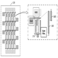
4 illustrates a structure and a circuit diagram of a photoreactive sensor-based sensor array according to an embodiment of the present invention.
More specifically, FIG. 4A illustrates a structure of a photoreactive sensor-based sensor array according to an embodiment of the present invention, and FIG. 4B illustrates a circuit diagram of a photoreactive sensor-based sensor array according to an embodiment of the present invention. It is.
Referring to FIG. 4A, the biometric information measuring apparatus using the sensor array of the present invention includes a
The
In addition, when a gate pulse signal of light scattered by the skin tissue is supplied to the switching
In addition, the
4B, in the photoreactive sensor-based sensor array, the gate of the switching
The photoreactive sensor-based sensor array can operate as a shift register while each bus line is connected to an external touch-out IC (R / O IC).
In addition, the gate line and the data line of the photoreactive sensor-based sensor array are connected to the gate driving circuit and the data driving circuit, respectively, and each connected line and circuit can receive the gate driving signal voltage and the input data signal voltage.
2, the average
The average
According to the embodiment, the average
The biometric information may be associated with tissue activity and function associated with at least one of heart rate and oxygen saturation. The biometric information may also be referred to as a pulse oximeter.
The
The
The
In addition, the average value of the biometric information measured through the biometric
The
For example, the
The
In addition, the
The power supply unit may supply the driving power of at least one of the
For example, the power supply unit may be composed of an active element using an ultra-small charge / discharge battery or a super-capacitor.
According to an embodiment, the power supply unit may be a secondary battery such as a coin battery or a secondary battery such as a lithium-polymer battery. When the power supply unit is a secondary battery, the power supply unit may be charged by an external power source When the supply portion is a primary battery such as a coin battery, it can be replaced.
At least one of the average
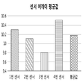
5 is a graph showing average values measured through a sensor array including a photoreactive sensor according to an embodiment of the present invention.
More specifically, FIG. 5 shows an average value of biometric information (pulse oximeter) measured from a bio-information measuring device including a single photoreactive sensor.
Referring to FIG. 5, the pulse oximeter value measured from the bio-information measuring device including the No. 1 sensor (photoreactivity sensor) is about 10.3, and from the bio-information measuring device including the No. 2 sensor The measured pulse oximeter value represents about 10.1.
Also, the pulse oximeter value measured from the bio-information measuring apparatus including the No. 3 sensor is about 9.8, and the pulse oximeter value measured from the bio-information measuring apparatus including the No. 4 sensor is about 10.5.
Although four sensors are illustrated in FIG. 5 as an example, the present invention is not limited to the above-described number of sensors and can be used without limitation.
That is, as shown in FIG. 5, the biometric information measuring apparatus including each single sensor changes the pulse oximeter value for the biological tissue to be measured by changing the pulse oximeter accuracy depending on the attachment position or area of the measurement target site It can be seen that there is a limit to accurate measurement.
Therefore, it can be seen that the accuracy and reliability of the average value of the calculated pulse oximeter is higher than that of the bio-information measuring apparatus composed of a single sensor, using a sensor array including a plurality of photoreactive sensors, Since the error due to external factors is small, it can be seen that the pulse oximeter with high accuracy for skin tissue can be measured uniformly.
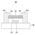
FIG. 6 illustrates an optical amplification phototransistor of a photoreactive sensor according to an embodiment of the present invention, and FIG. 7 illustrates a circuit configuration of an optical amplification phototransistor of a photoreactive sensor according to an embodiment of the present invention.
The optical amplification phototransistor of the present invention includes a channel region including a gate electrode, a source electrode, a drain electrode, and a channel region including a non-overlapped region that is not overlapped with the gate electrode and between the source electrode and the drain electrode And the non-overlap region operates as a photo conductor for amplifying photoconductivity.
According to an embodiment, the gate electrode may be a local top gate structure or a local bottom gate structure.
6, an
A local
A source electrode 185S and a
The source electrode 185S and the
According to an embodiment, the local
The
As shown in FIG. 7, the
The
Two-dimensional materials are relatively easy to fabricate when compared to one-dimensional materials, making them suitable for use as materials for next-generation nanoelectronic devices. Of these two-dimensional materials, 2D transition metal dichalcogenides include molybdenum disulfide (MoS2), molybdenum diselenide (MoSe2), tungsten diselenide (WSe2), and molybdenum diselenide Molybdenum Ditelluride (MoTe2), and tin diselenide (SnSe2).
In addition, the two-dimensional transition metal chalcogenide compound can absorb light of wavelengths below 1500 nm because it has a band gap generally below 2 eV.
Although the
In the
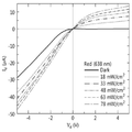
8 is a graph showing characteristics of a photoconductor of an optical amplification phototransistor according to an embodiment of the present invention. FIG. 8A is a characteristic graph when green light (532 nm) is irradiated, and FIG. 8B is a characteristic graph when red light (638 nm) is irradiated.
Referring to FIG. 8, when the light is irradiated, the optical amplification phototransistor according to the embodiment of the present invention shows a tendency that the resistance is lowered and the conductivity is increased in comparison with the case where no light is irradiated. Further, the larger the wavelength of the irradiated light, the larger the magnitude of the drain current.
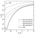
FIG. 9 shows a transfer curve graph of an optical amplification phototransistor according to an embodiment of the present invention, and FIG. 10 shows a graph of photoreactive characteristics.
Referring to FIGS. 9 and 10, when a light is applied, not only a channel region where an electron-hole pair overlaps a local gate electrode, but also a non-overlap region of a channel region acting as a photoconductor As a result, the conductivity of the entire channel is amplified, and not only the off-current of the phototransistor but also the on-current largely increases.
As shown in FIGS. 9 and 10, the optical amplifying phototransistor including the local gate electrode structure of the present invention is formed by a conventional technique having a common gate structure (Woong Choi, et. Al , Advanced Materials 24, 5382-5836 (2012)), the photoreactivity of about 100 to 1000 times higher than that of 100 mAW-1 is amplified.
As shown in FIGS. 8 to 10, the optical amplifying phototransistor of the present invention can amplify optical gain and photoreactivity through a structure in which a photoconductor and a phototransistor are combined by forming a local gate electrode.
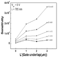
11 illustrates the sensitivity of the optical amplification phototransistor according to the non-overlap length according to the embodiment of the present invention. Referring to FIG. 11, it can be seen that the sensitivity increases according to the non-overlap length and the photoreactivity. Therefore, the apparatus for measuring bio-information using the sensor array according to the embodiment of the present invention can provide a photoreactive sensor including a non-overlap region to amplify optical gain and photoreactivity.
While the present invention has been particularly shown and described with reference to exemplary embodiments thereof, it is to be understood that the invention is not limited to the disclosed exemplary embodiments. For example, it is to be understood that the techniques described may be performed in a different order than the described methods, and / or that components of the described systems, structures, devices, circuits, Lt; / RTI > or equivalents, even if it is replaced or replaced.
Therefore, other implementations, other embodiments, and equivalents to the claims are also within the scope of the following claims.
100: Biometric information measuring device using sensor array
120: sensor array
200: terminal
Claims (9)
And a photodetector coupled to the switching thin film transistor for amplifying photoreactivity of light generated from the light source unit and reflected or transmitted from the skin tissue, wherein the photoreactivity amplifies the tissue activity and function of the skin tissue, A sensor array formed on the substrate, the sensor array including a plurality of photoreactive sensors for outputting absorption information for mapping biometric information associated with the sensor; And
And an average value measuring unit for measuring an average value of the biometric information for the sensor array based on the absorption information output from the photoreactive sensor,
Wherein the biometric information measuring device is a biometric information measuring device using a sensor array.
The photoreactive sensor
One or more optical amplification phototransistors arranged in an active matrix form
Wherein the biometric information measuring device is a biometric information measuring device using a sensor array.
The optical amplification phototransistor
A channel region including a local gate electrode, a source electrode, a drain electrode, and a channel region including a nonoverlap region not overlapping the gate electrode, the channel region being formed between the source electrode and the drain electrode,
Wherein the non-overlapped region operates as a photoconductor for amplifying photoconductivity.
Wherein the nonoverlap region is formed in both lateral directions of the source electrode and the drain electrode, or is formed in any one of the lateral direction of the source electrode and the drain electrode.
The channel region
And a transition metal chalcogenide compound (Transition Metal Dichalcogenides).
The biometric information
Heart rate, oxygen saturation, and / or heart rate. The apparatus for measuring bio-information using a sensor array according to claim 1,
The sensor array
And is formed in a patch-like structure in connection with an IC circuit formed on the substrate.
The substrate
Wherein the biometric information measuring device is formed of at least one of paper, polymer, woven fabric, and metal foil.
A communication module for transmitting an average value of the measured biometric information to the outside; And
And an average value of the biometric information from the average value measuring unit based on absorption information measured from at least one photoreactive sensor selected from among the plurality of photoreactive sensors in response to a control command received from the communication module A control unit
Wherein the biometric information measuring device further comprises a sensor array.
Priority Applications (5)
| Application Number | Priority Date | Filing Date | Title |
|---|---|---|---|
| KR1020150180337A KR101779264B1 (en) | 2015-12-16 | 2015-12-16 | Biological information measurement device using sensor array |
| PCT/KR2016/000160 WO2017086537A1 (en) | 2015-11-17 | 2016-01-08 | Device and method for measuring biological information by using sensor array |
| CN201680079251.0A CN108770336B (en) | 2015-11-17 | 2016-01-08 | Biological information measuring apparatus and method using sensor array |
| US15/777,057 US11129555B2 (en) | 2015-11-17 | 2016-01-08 | Device for measuring biological information including sensor array and method of measuring biological information using device |
| US17/089,273 US11911153B2 (en) | 2015-11-17 | 2020-11-04 | Device for measuring biological information including sensor array and method of measuring biological information using device |
Applications Claiming Priority (1)
| Application Number | Priority Date | Filing Date | Title |
|---|---|---|---|
| KR1020150180337A KR101779264B1 (en) | 2015-12-16 | 2015-12-16 | Biological information measurement device using sensor array |
Publications (2)
| Publication Number | Publication Date |
|---|---|
| KR20170072018A true KR20170072018A (en) | 2017-06-26 |
| KR101779264B1 KR101779264B1 (en) | 2017-09-18 |
Family
ID=59282292
Family Applications (1)
| Application Number | Title | Priority Date | Filing Date |
|---|---|---|---|
| KR1020150180337A KR101779264B1 (en) | 2015-11-17 | 2015-12-16 | Biological information measurement device using sensor array |
Country Status (1)
| Country | Link |
|---|---|
| KR (1) | KR101779264B1 (en) |
Cited By (6)
| Publication number | Priority date | Publication date | Assignee | Title |
|---|---|---|---|---|
| KR20190032242A (en) * | 2017-09-18 | 2019-03-27 | 고려대학교 세종산학협력단 | Stretchable multimodal sensor and method of fabricating of the same |
| KR102178417B1 (en) * | 2019-08-22 | 2020-11-13 | 한국표준과학연구원 | Method for detecting Vitamin D in blood using LDI-MS and apparatus for same |
| KR20210016760A (en) | 2019-08-05 | 2021-02-17 | 연세대학교 산학협력단 | Bio-signal measuring device having array patterns of ultra small electrode |
| KR20220001601A (en) | 2020-06-30 | 2022-01-06 | 연세대학교 산학협력단 | Neural Signal Feedback System and Method having array patterns of ultra small electrode |
| KR20220001600A (en) | 2020-06-30 | 2022-01-06 | 연세대학교 산학협력단 | Variable Frequency typed Bio-signal measuring device having array patterns of ultra small electrode and Health Care system using the same decive |
| KR20220060802A (en) * | 2020-11-05 | 2022-05-12 | 주식회사 휴서카디안 | Apparatus and method for managing circadian rhythm based on feedback function |
Families Citing this family (1)
| Publication number | Priority date | Publication date | Assignee | Title |
|---|---|---|---|---|
| US11781217B2 (en) | 2018-12-31 | 2023-10-10 | Industry-Academic Cooperation Foundation, Yonsei University | Transient sensor using molybdenum disulfide and method of manufacturing the same |
Family Cites Families (1)
| Publication number | Priority date | Publication date | Assignee | Title |
|---|---|---|---|---|
| JP4348467B2 (en) * | 2003-09-30 | 2009-10-21 | 学校法人日本大学 | Biological material property inspection system using light |
-
2015
- 2015-12-16 KR KR1020150180337A patent/KR101779264B1/en active IP Right Grant
Cited By (7)
| Publication number | Priority date | Publication date | Assignee | Title |
|---|---|---|---|---|
| KR20190032242A (en) * | 2017-09-18 | 2019-03-27 | 고려대학교 세종산학협력단 | Stretchable multimodal sensor and method of fabricating of the same |
| KR20210016760A (en) | 2019-08-05 | 2021-02-17 | 연세대학교 산학협력단 | Bio-signal measuring device having array patterns of ultra small electrode |
| KR20210137962A (en) | 2019-08-05 | 2021-11-18 | 연세대학교 산학협력단 | Bio-signal measuring device having array patterns of ultra small electrode |
| KR102178417B1 (en) * | 2019-08-22 | 2020-11-13 | 한국표준과학연구원 | Method for detecting Vitamin D in blood using LDI-MS and apparatus for same |
| KR20220001601A (en) | 2020-06-30 | 2022-01-06 | 연세대학교 산학협력단 | Neural Signal Feedback System and Method having array patterns of ultra small electrode |
| KR20220001600A (en) | 2020-06-30 | 2022-01-06 | 연세대학교 산학협력단 | Variable Frequency typed Bio-signal measuring device having array patterns of ultra small electrode and Health Care system using the same decive |
| KR20220060802A (en) * | 2020-11-05 | 2022-05-12 | 주식회사 휴서카디안 | Apparatus and method for managing circadian rhythm based on feedback function |
Also Published As
| Publication number | Publication date |
|---|---|
| KR101779264B1 (en) | 2017-09-18 |
Similar Documents
| Publication | Publication Date | Title |
|---|---|---|
| KR101779264B1 (en) | Biological information measurement device using sensor array | |
| US20220409069A1 (en) | Methods and systems for detecting physiology for monitoring cardiac health | |
| Wang et al. | Skin bioelectronics towards long-term, continuous health monitoring | |
| US11029198B2 (en) | Alternative approach for UV sensing | |
| ES2813111T3 (en) | Microelectronic sensors for non-invasive monitoring of physiological parameters | |
| EP3397139B1 (en) | Device, system and method for non-invasive monitoring of physiological measurements | |
| US20210068718A1 (en) | Device for measuring biological information including sensor array and method of measuring biological information using device | |
| Rodriguez-Labra et al. | Development of a PPG sensor array as a wearable device for monitoring cardiovascular metrics | |
| KR102649561B1 (en) | Non-Invasive Biometric Sensor Based on Organic Photodetector | |
| Herrmann et al. | Prostheses control with combined near-infrared and myoelectric signals | |
| KR101596195B1 (en) | Artificial skin sensor and bioinformation diagnostic apparatus based on artificial skin sensor | |
| US11918331B2 (en) | Micro-movement and gesture detection using radar | |
| US11432774B2 (en) | Pulse oximeters and pulse oximeter embedded organic image sensors | |
| US20170049395A1 (en) | Neuro-vigilance integrated contact eye lens and system | |
| US11129571B2 (en) | Cardiac waveform sensing | |
| CN114376532B (en) | Reflection type photoplethysmography sensor and biological information measuring device | |
| CN114391816A (en) | Intelligent health monitoring patch | |
| Sharma et al. | Circuits and systems for energy efficient smart wearables | |
| WO2022071028A1 (en) | Biological condition diagnosis system | |
| US20240120326A1 (en) | Bio sensing device | |
| Kim et al. | Nonintrusive measurement of heart rate using a flexible sensor array | |
| US20240206817A1 (en) | Integrated sensing platform | |
| US20230240602A1 (en) | Inducing hypoxia to monitor one or more patient conditions using a medical device system | |
| Divya et al. | Design and Development of a Non-Invasive Glucose Monitoring Device Using Advanced Microcontroller | |
| Serbanescu et al. | Architecture for a Modular Temperature Detection System Used for Diabetic Foot Investigations |
Legal Events
| Date | Code | Title | Description |
|---|---|---|---|
| A201 | Request for examination | ||
| E902 | Notification of reason for refusal | ||
| E701 | Decision to grant or registration of patent right | ||
| GRNT | Written decision to grant |