KR20170061160A - A non-volatile split gate memory device and a method of operating same - Google Patents
A non-volatile split gate memory device and a method of operating same Download PDFInfo
- Publication number
- KR20170061160A KR20170061160A KR1020177011636A KR20177011636A KR20170061160A KR 20170061160 A KR20170061160 A KR 20170061160A KR 1020177011636 A KR1020177011636 A KR 1020177011636A KR 20177011636 A KR20177011636 A KR 20177011636A KR 20170061160 A KR20170061160 A KR 20170061160A
- Authority
- KR
- South Korea
- Prior art keywords
- region
- voltage
- negative
- memory cells
- word line
- Prior art date
Links
Images


Classifications
-
- G—PHYSICS
- G11—INFORMATION STORAGE
- G11C—STATIC STORES
- G11C16/00—Erasable programmable read-only memories
- G11C16/02—Erasable programmable read-only memories electrically programmable
- G11C16/06—Auxiliary circuits, e.g. for writing into memory
- G11C16/24—Bit-line control circuits
-
- G—PHYSICS
- G11—INFORMATION STORAGE
- G11C—STATIC STORES
- G11C16/00—Erasable programmable read-only memories
- G11C16/02—Erasable programmable read-only memories electrically programmable
- G11C16/04—Erasable programmable read-only memories electrically programmable using variable threshold transistors, e.g. FAMOS
- G11C16/0408—Erasable programmable read-only memories electrically programmable using variable threshold transistors, e.g. FAMOS comprising cells containing floating gate transistors
- G11C16/0425—Erasable programmable read-only memories electrically programmable using variable threshold transistors, e.g. FAMOS comprising cells containing floating gate transistors comprising cells containing a merged floating gate and select transistor
-
- G—PHYSICS
- G11—INFORMATION STORAGE
- G11C—STATIC STORES
- G11C16/00—Erasable programmable read-only memories
- G11C16/02—Erasable programmable read-only memories electrically programmable
- G11C16/06—Auxiliary circuits, e.g. for writing into memory
- G11C16/10—Programming or data input circuits
- G11C16/12—Programming voltage switching circuits
-
- G—PHYSICS
- G11—INFORMATION STORAGE
- G11C—STATIC STORES
- G11C16/00—Erasable programmable read-only memories
- G11C16/02—Erasable programmable read-only memories electrically programmable
- G11C16/06—Auxiliary circuits, e.g. for writing into memory
- G11C16/10—Programming or data input circuits
- G11C16/14—Circuits for erasing electrically, e.g. erase voltage switching circuits
-
- G—PHYSICS
- G11—INFORMATION STORAGE
- G11C—STATIC STORES
- G11C16/00—Erasable programmable read-only memories
- G11C16/02—Erasable programmable read-only memories electrically programmable
- G11C16/06—Auxiliary circuits, e.g. for writing into memory
- G11C16/26—Sensing or reading circuits; Data output circuits
-
- G—PHYSICS
- G11—INFORMATION STORAGE
- G11C—STATIC STORES
- G11C16/00—Erasable programmable read-only memories
- G11C16/02—Erasable programmable read-only memories electrically programmable
- G11C16/06—Auxiliary circuits, e.g. for writing into memory
- G11C16/10—Programming or data input circuits
Abstract
제1 도전성 타입의 반도체 기판을 갖는 비휘발성 메모리 디바이스가 개시된다. 비휘발성 메모리 셀들의 어레이가 반도체 기판에 복수의 행들 및 열들로 배열되어 있다. 각각의 메모리 셀은 제2 도전성 타입의 반도체 기판의 표면 상의 제1 영역, 및 제2 도전성 타입의 반도체 기판의 표면 상의 제2 영역을 포함한다. 제1 영역과 제2 영역 사이에는 채널 영역이 있다. 워드 라인은 채널 영역의 제1 부분 위에 놓여 있고, 그로부터 절연되며, 제1 영역에 인접하고, 제1 영역과 거의 또는 전혀 중첩되지 않는다. 플로팅 게이트가 채널 영역의 제2 부분 위에 놓여 있고, 제1 부분에 인접하고, 그로부터 절연되고 제2 영역에 인접한다. 커플링 게이트가 플로팅 게이트 위에 놓여 있다. 비트 라인이 제1 영역에 접속된다. 네거티브 전하 펌프 회로가 제1 네거티브 전압을 발생시킨다. 제어 회로가 커맨드 신호를 수신하고, 이에 응답하여 복수의 제어 신호들을 발생시키고, 제1 네거티브 전압을 비선택된 메모리 셀들의 워드 라인에 인가한다. 프로그래밍, 판독, 또는 소거의 동작들 동안, 네거티브 전압이 비선택된 메모리 셀들의 워드 라인들에 인가될 수 있다.A non-volatile memory device having a semiconductor substrate of a first conductivity type is disclosed. An array of non-volatile memory cells is arranged in a plurality of rows and columns in a semiconductor substrate. Each memory cell includes a first region on the surface of the semiconductor substrate of the second conductivity type and a second region on the surface of the semiconductor substrate of the second conductivity type. There is a channel region between the first region and the second region. The word lines are overlying, insulated from, and adjacent to the first region of the channel region, and do not overlap with the first region at all or at all. A floating gate overlies the second portion of the channel region, adjacent to the first portion, insulated therefrom, and adjacent to the second region. The coupling gate lies on the floating gate. A bit line is connected to the first region. A negative charge pump circuit generates a first negative voltage. A control circuit receives the command signal, generates a plurality of control signals in response thereto, and applies a first negative voltage to the word line of the unselected memory cells. During programming, reading, or erasing operations, a negative voltage may be applied to the word lines of unselected memory cells.
Description
본 발명은 비휘발성 메모리 셀 디바이스 및 그의 동작 방법에 관한 것이다. 더 구체적으로, 본 발명은 판독, 프로그래밍 또는 소거의 동작들 동안 네거티브 전압이 제어 게이트 및/또는 워드 라인(word line)에 인가되고, 메모리 셀들의 다른 단자들과 선택적으로 조합하는, 그러한 메모리 디바이스에 관한 것이다.The present invention relates to non-volatile memory cell devices and methods of operation thereof. More particularly, the present invention relates to such memory devices in which a negative voltage is applied to the control gate and / or word line during read, program or erase operations and is selectively combined with other terminals of memory cells .
비휘발성 메모리 셀들은 본 기술 분야에 잘 알려져 있다. 종래 기술의 하나의 비휘발성 분리형 게이트 메모리 셀(10)이 도 1에 도시되어 있다. 메모리 셀(10)은 P 타입과 같은 제1 전도성 타입의 반도체 기판(12)을 포함한다. 기판(12)은 N 타입과 같은 제2 도전성 타입의 제1 영역(14)(또한 소스 라인(source line, SL)으로도 알려짐)이 형성된 표면을 갖는다. 또한 N 타입의 제2 영역(16)(또한, 드레인 라인(drain line)으로도 알려짐)이 기판(12)의 표면 상에 형성된다. 제1 영역(14)과 제2 영역(16) 사이에는 채널 영역(18)이 있다. 비트 라인(bit line, BL)(20)이 제2 영역(16)에 접속된다. 워드 라인(WL)(22)이 채널 영역(18)의 제1 부분 위에 위치되고 그로부터 절연된다. 워드 라인(22)은 제2 영역(16)과 거의 또는 전혀 중첩되지 않는다. 플로팅 게이트(floating gate, FG)(24)가 채널 영역(18)의 다른 부분 위에 있다. 플로팅 게이트(24)는 그로부터 절연되고, 워드 라인(22)에 인접한다. 플로팅 게이트(24)는 또한 제1 영역(14)에 인접한다. 커플링 게이트(coupling gate, CG)(26)(또한 제어 게이트로도 알려짐)가 플로팅 게이트(24) 위에 있고 그로부터 절연된다. SL 폴리(28)가 제1 영역(14)(소스 라인(SL))에 접속된다.Non-volatile memory cells are well known in the art. One prior art non-volatile detachable
종래 기술에서, 포지티브 또는 0(zero) 전압들의 다양한 조합들이 워드 라인(22), 커플링 게이트(26), 및 플로팅 게이트(24)에 판독, 프로그래밍, 및 소거 동작들을 수행하도록 인가되었다. 종래 기술은 이들 동작들에 대해 네거티브 전압들을 인가하지 않았다.In the prior art, various combinations of positive or zero voltages have been enabled to perform read, program, and erase operations on the
본 발명의 하나의 목적은 판독, 프로그래밍, 및/또는 소거 동작들 동안 네거티브 전압을 워드 라인(22), 커플링 게이트(26), 및/또는 플로팅 게이트(24)에 인가하는 비휘발성 메모리 셀 디바이스를 개시하는 것이다.One object of the present invention is to provide a nonvolatile memory cell device (not shown) that applies a negative voltage to
본 발명은 제1 도전성 타입의 반도체 기판을 갖는 비휘발성 메모리 디바이스에 관한 것이다. 비휘발성 메모리 셀들의 어레이가 반도체 기판에 복수의 행(row)들 및 열(column)들로 배열되어 있다. 각각의 메모리 셀은 제2 도전성 타입의 반도체 기판의 표면 상의 제1 영역, 및 제2 도전성 타입의 반도체 기판의 표면 상의 제2 영역을 포함한다. 제1 영역과 제2 영역 사이에는 채널 영역이 있다. 워드 라인은 채널 영역의 제1 부분 위에 놓여 있고, 그로부터 절연되며, 제1 영역에 인접하고, 제1 영역과 거의 또는 전혀 중첩되지 않는다. 워드 라인은 플로팅 게이트의 상측 팁(tip) 코너(도 1에서의 팁 코너(25))에 대면하는 저부 아크 영역(도 1에서의 영역(27))을 갖는다. 플로팅 게이트는 채널 영역의 제2 부분 위에 놓여 있고, 제1 부분에 인접하고, 그로부터 절연되고 제2 영역에 인접한다. 커플링 게이트가 플로팅 게이트 위에 놓여 있다. 비트 라인이 제1 영역에 접속된다. 네거티브 전하 펌프 회로(negative charge pump circuit)가 제1 네거티브 전압을 발생시킨다. 제어 회로가 커맨드 신호를 수신하고, 이에 응답하여 복수의 제어 신호들을 발생시키고, 제1 네거티브 전압을 비선택된 메모리 셀들의 워드 라인에 인가한다.The present invention relates to a non-volatile memory device having a semiconductor substrate of a first conductivity type. An array of non-volatile memory cells is arranged in a plurality of rows and columns in a semiconductor substrate. Each memory cell includes a first region on the surface of the semiconductor substrate of the second conductivity type and a second region on the surface of the semiconductor substrate of the second conductivity type. There is a channel region between the first region and the second region. The word lines are overlying, insulated from, and adjacent to the first region of the channel region, and do not overlap with the first region at all or at all. The word line has a bottom arc region (
본 발명은 또한 전술한 타입의 비휘발성 메모리 셀 디바이스의 동작 방법에 관한 것이다.The present invention also relates to a method of operating a non-volatile memory cell device of the type described above.
도 1은 본 발명의 방법이 적용될 수 있는 종래 기술의 비휘발성 메모리 셀의 단면도이다.
도 2는 도 1에 도시된 종래 기술의 비휘발성 메모리 셀을 사용하는 본 발명의 비휘발성 메모리 디바이스의 블록 다이어그램이다.
도 3a 및 도 3b는 각각 본 발명의 메모리 디바이스에서 사용하기 위한 프로그래밍/소거 및 판독 동작들의 파형도들이다.
도 4a 및 도 4b는 각각 본 발명의 메모리 디바이스에서 사용하기 위한 네거티브/포지티브 워드 라인 디코더 회로(negative/positive word line decoder circuit) 및 네거티브 전하 펌프의 상세 회로 다이어그램들이다.
도 5는 본 발명의 메모리 디바이스에서 사용하기 위한 제1 네거티브/포지티브 고전압 디코더 회로의 상세 회로 다이어그램이다.
도 6은 본 발명의 메모리 디바이스에서 사용하기 위한 제2 네거티브/포지티브 고전압 디코더 회로의 상세 회로 다이어그램이다.
도 7은 본 발명의 메모리 디바이스에서 사용하기 위한 제3 네거티브/포지티브 고전압 디코더 회로의 상세 회로 다이어그램이다.
도 8은 본 발명의 메모리 디바이스와 함께 사용하기 위한 네거티브 전압 전하 펌프 발생기의 상세 회로 다이어그램이다.
도 9는 본 발명의 메모리 디바이스에서 사용하기 위한 네거티브 고전압 조정 회로(regulation circuit)의 상세 회로 다이어그램이다.
도 10은 본 발명의 메모리 디바이스에서 사용하기 위한 네거티브/포지티브 패드 회로(pad circuit)의 상세 회로 다이어그램이다.
도 11a 및 도 11b는 종래 기술의 메모리 디바이스를 제조하는 데 사용하기 위한 종래 기술의 프로세스 흐름의 일부를 도시한 단면도들이다.
도 11c는 본 발명의 메모리 디바이스를 제조하기 위한 프로세스 흐름의 일부를 도시한 단면도이다.1 is a cross-sectional view of a prior art nonvolatile memory cell to which the method of the present invention may be applied.
2 is a block diagram of a non-volatile memory device of the present invention using the prior art non-volatile memory cell shown in FIG.
3A and 3B are waveform diagrams of programming / erasing and reading operations for use in the memory device of the present invention, respectively.
4A and 4B are detailed circuit diagrams of a negative / positive word line decoder circuit (negative / positive word line decoder circuit) and a negative charge pump for use in the memory device of the present invention, respectively.
5 is a detailed circuit diagram of a first negative / positive high voltage decoder circuit for use in a memory device of the present invention.
6 is a detailed circuit diagram of a second negative / positive high voltage decoder circuit for use in a memory device of the present invention.
7 is a detailed circuit diagram of a third negative / positive high voltage decoder circuit for use in a memory device of the present invention.
Figure 8 is a detailed circuit diagram of a negative voltage charge pump generator for use with a memory device of the present invention.
Figure 9 is a detailed circuit diagram of a negative high voltage regulation circuit for use in the memory device of the present invention.
10 is a detailed circuit diagram of a negative / positive pad circuit for use in the memory device of the present invention.
11A and 11B are cross-sectional views illustrating a portion of a prior art process flow for use in fabricating a prior art memory device.
11C is a cross-sectional view illustrating a portion of a process flow for fabricating a memory device of the present invention.
도 2를 참조하면, 본 발명의 비휘발성 메모리 디바이스(50)의 블록 레벨 다이어그램이 도시되어 있다. 도 2에 도시된 실시예에서, 메모리 디바이스(50)는 도 1에 도시된 타입의, 반도체 기판(12) 내에 복수의 행들 및 열들로 배열된 비휘발성 메모리 셀들(10)의 2개의 어레이들(52A, 52B)을 포함한다. 비휘발성 메모리 셀들(10)의 각각의 어레이(52)에 인접하여, 선택된 및 비선택된 메모리 셀들(10)의 워드 라인들(22)에 디코딩되어 공급되는 어드레스 신호들을 수신하기 위한 디코더(각각, X디코더(54A, 54B))가 있다. 디코더들(54)의 각각은 또한 네거티브 전압을 발생시키기 위해 전하 펌프(56)에 포함된 연관된 네거티브 전하 펌프를 갖는다. 어레이들(52A, 52B) 사이에 배치되는 디코더(WSHDRHALFV, NCG)(80)는 도 5 내지 도 7의 실시예들에 도시된 바와 같이 제어 게이트(26) 및 소스 라인(14)을 위한 전압 레벨들을 제공한다.Referring to FIG. 2, a block level diagram of a
메모리 디바이스(50)의 메모리 어레이들(52)의 각각은, 또한, 어레이(52)의 메모리 셀들(10)로부터 신호들을 수신하고 디바이스(50)로부터 출력 신호들을 발생시키기 위해 그와 연관된 복수의 센서들(58)을 갖는다. 메모리 디바이스(50)는 또한 로직 회로(60)를 갖는다. 로직 회로(60)는 메모리 디바이스(50)가 다양한 커맨드들을 실행하도록 하기 위해 메모리 디바이스(50) 외부의 호스트 제어기(미도시)에서 발행되는 프로그래밍, 소거 또는 판독과 같은 커맨드들을 수신한다. 수신된 커맨드들에 응답하여, 로직 회로(50)는 전하 펌프 회로들(56) 및 디코딩 회로들(54)의 동작 및 타이밍을 제어하고, 증폭 회로들(58)을 감지하는 제어 신호들을 발생시킨다. 아날로그 회로(70)는 디바이스(50)에 아날로그 바이어스 전압들과 전류들 그리고 타이밍을 제공한다. 고전압(포지티브, 네거티브) 제어 회로(90)는 조정되고 시간 순서로 정렬된(regulated and time-sequenced) 포지티브 및 네거티브 레벨들을 제공한다. 패드 회로(88)는 입력 버퍼들, IO 버퍼들, 전력 패드들(Vdd, Vss), 테스트 패드들 및 ESD 보호를 제공한다.Each of the memory arrays 52 of the
판독, 소거 또는 프로그래밍 커맨드에 응답하여, 로직 회로(60)는 다양한 전압이 선택된 메모리 셀(10) 및 비선택된 메모리 셀들(10) 모두의 다양한 부분들에 시기적절하고 최소의 교란(disturb) 방식으로 공급되도록 한다.In response to a read, erase, or programming command, the logic circuit 60 is programmed to cause the various voltages to be applied to various portions of both the
선택된 및 비선택된 메모리 셀(10)에 대해, 인가된 전압과 전류는 다음과 같다. 이후에 사용되는 바와 같이, 하기의 약어들, 즉 소스 라인 또는 제1 영역(14)(SL), 비트 라인(20)(BL), 워드 라인(22)(WL), 및 커플링 게이트(26)(CG)가 사용된다.For selected and


비휘발성 메모리 셀(10)의 소거 및 프로그래밍에 대한 동작은 다음과 같다. 셀(10)은 다른 단자들이 0 볼트 또는 네거티브인 상태에서 워드 라인(22) 상에 고전압을 인가함으로써 파울러-노드하임 터널링 메커니즘을 통해 소거된다. 전자들은 플로팅 게이트(24)로부터 워드 라인(22) 내로 터널링하여 포지티브로 대전되게 하여, 셀(10)을 판독 상태에서 턴온시킨다. 터널링은 FG 팁(25)으로부터 WL(22)의 아크 랩어라운드 영역(27)까지이다. 생성된 셀 소거 상태는 '1' 상태로 알려져 있다. 셀(10)은, 커플링 게이트(26) 상에 고전압을, 소스 라인(14) 상에 고전압을, 그리고 비트 라인(20) 상에 프로그래밍 전류를 인가함으로써, 소스측 열전자 프로그래밍 메커니즘을 통해 프로그래밍된다. 워드 라인(22)과 플로팅 게이트(24) 사이의 갭을 가로질러서 유동하는 전자들 중 일부는 플로팅 게이트(24) 내에 주입하기에 충분한 에너지를 획득하여 플로팅 게이트(24)가 네거티브로 대전되게 하여, 셀(10)을 판독 조건에서 턴오프시킨다. 생성된 셀 프로그래밍 상태는 '0' 상태로 알려져 있다. 판독 동작은 비트 라인(20) 상에 포지티브 바이어스를, WL(22) 상에 포지티브 바이어스를, 소스 라인(14) 상에 0 볼트를, 그리고 커플링 게이트(26) 상에 포지티브 또는 0 볼트를 인가함으로써 행해진다. 이러한 판독 조건에서, 상태 '1'을 갖는 메모리 셀이 전류를 도통시키고, 상태 '0'을 갖는 메모리 셀이 전류 레벨을 전혀 도통시키지 않거나 또는 낮은 전류 레벨을 도통시킨다. 비선택된 WL들의 경우, 0 또는 네거티브 전압이 판독 및 프로그래밍 조건을 위해 인가될 수 있다.The operation for erasing and programming the
소거 동작 #3에서, WL은 포지티브 HV, 예컨대 9 내지 6 V에 있고, CG는 네거티브 HV, 예컨대 -(5 내지 9) V에 있다. 비선택된 WL은 0 V 또는 네거티브 전압, 예컨대 -(0.5 내지 5) V에 있고, 비선택된 CG는 0 V 또는 네거티브 HV, 예컨대 -(5 내지 9) V(선택된 네거티브 CG HV 전압과 동일함)에 있을 수 있다.In erase
대안으로, 프로그래밍 동작이 수행될 수 있는데, P 기판(Vsub)(12)은 0 V 대신에 네거티브, 예컨대 -6 V이다.Alternatively, a programming operation may be performed, wherein the P substrate (Vsub) 12 is negative, e.g., -6 V instead of 0 V.
도 3a를 참조하면, 본 발명의 메모리 디바이스(50)에서 사용하기 위한 상기한 바와 같은 포지티브/네거티브 바이어스 레벨들을 위한 프로그래밍 및 소거 신호들에 대한 신호 타이밍 파형의 일례가 도시되어 있다. 메모리 셀(10)의 단자들 WL, BL, CG, SL에 각각 대응하는 바와 같은 신호들 WL, BL, CG, SL은 전술된 바와 같다. 프로그래밍을 위해, (예컨대, 후술될 디코더 회로(80) 내에서 제어 신호를 설정하기 위해) 신호 WL(102)이 먼저 하이(high)(예컨대, ~Vdd)가 되고, 이어서 (바이어스 전압(Vpwl)으로) 정착(settle down)하기 시작한다. 이어서, 신호 BL(104) 및 CG(106)는 각각 하이, 예컨대, ~Vinh =~ Vdd 및 10 내지 11 V로 되고, 이어서 SL(110)은 하이(예컨대, ~ 4.5 V 내지 5 V)가 된다. 대안으로, CG(106)는 SL(110) 후에 하이가 된다(점선으로 된 파형으로 도시된 바와 같음). 신호 WL(102)은 전압 Vpwl, 예컨대 1 V로 정착되고, 신호 BL(104)은 CG가 하이가 될 때 전압 Vdp, 예컨대 ~0.5 V로 정착된다. 비선택된 WL들은 선택된 WL(102)이 하이가 되기 전 또는 이와 동시에 0 V 또는 네거티브, 예컨대 -0.5 V로 하강한다. 비선택된 CG들은 대기 상태의 값, 예컨대 0 내지 2.6 V에 머무른다. 비선택된 SL들은, CG(106)가 하이가 될 때, 대기 상태의 값, 예컨대 0 V에 머무르거나, 또는 바이어스 전압, 예컨대 1 V로 전환된다(비선택된 SL이 바이어스 레벨로 전환되어 BL들을 통하여 비선택된 셀들을 통한 누설 전류를 방지한다).Referring to FIG. 3A, an example of a signal timing waveform for programming and erasing signals for positive / negative bias levels as described above for use in the
다양한 신호들이 프로그래밍 전압들로 램핑(ramping)하는 동안 아직 정착되지 않음으로 인한 의도하지 않은 프로그램 교란을 방지하기 위해 신호 BL(104)이 먼저 Vinh(금지 전압(inhibit voltage))로 하이가 된다. 타이밍 시퀀스 CG(106) 대 SL(110)이 교란 효과를 감소시키도록 최적화되는데, 예컨대 어느 신호든 더 많은 교란을 야기하는 신호가 마지막에 하이가 된다. 프로그래밍 펄스들의 램핑 다운은 교란을 최소화하기 위해 반전된다(즉, 먼저 상승한 신호가 이제 마지막에 하강한다). 신호 SL(110)이 하강하고, 이어서 CG(106)가 하강하고, 이어서 WL(102) 및 BL(104)이 하강한다. 기판 P가 네거티브로, 예컨대 -1 V로 되는 프로그래밍의 실시예에서, 이러한 네거티브 전환은 신호 WL이 로우(low)가 되거나 또는 CG가 하이가 되는 것과 동시에 일어난다.
소거를 위해, (예컨대, 도 5 내지 도 7의 실시예들에서와 같이 후술될 디코더 회로(80)에서 제어 신호를 설정하기 위해) 신호 WL(102)이 하이, 예컨대 Vdd가 되고, 이어서 로우, 예컨대 0 V(또는, 대안적으로, -0.5 V와 같은 네거티브)가 된다. WL(102)이 로우가 되는 것과 거의 동시에 또는 그 후의 단시간에, 신호 CG(106)는 네거티브, 예컨대 -6 V 내지 -9 V가 된다. 이어서, 선택된 WL(102)은 하이, 예컨대 9 V 내지 6 V가 된다. 신호들 BL(104) 및 SL(110)은 대기 상태의 값, 예컨대 0 V에 머무른다. 비선택된 WL들은 선택된 WL(102)이 하이가 되기 전 또는 이와 동시에 0V 또는 네거티브, 예컨대 -0.5 V로 하강한다. 비선택된 CG들은 대기 상태의 값, 예컨대 0 내지 2.6 V에 머무른다. 비선택된 SL들은 대기 상태의 값, 예컨대 0 V에 머무른다.For erasing, signal
소거의 다른 실시예에서, 기판 P는 네거티브, 예컨대 -6 V가 된다.In another embodiment of the erase, the substrate P is negative, e.g., -6 volts.
소거 펄스들의 램핑 다운은 대략 차례로 반전된다(즉, 먼저 상승한 신호가 이제 마지막에 하강한다). 신호들 WL(102) 및 CG(106)는 대기 상태의 값, 예컨대 0 V가 된다.The ramping down of the erase pulses is inverted approximately in turn (i. E., The first raised signal is now falling at the end). The
도 3b를 참조하면, 본 발명의 메모리 디바이스(50)에서 사용하기 위한, 상기한 바와 같은 포지티브/네거티브 바이어스 레벨들을 위한 판독 신호들에 대한 신호 타이밍 파형의 일례가 도시되어 있다. 이러한 판독 신호 파형은 완전한 비휘발성 소거/프로그래밍/판독 동작을 위해 도 3a의 프로그래밍 및 소거 신호 파형과 함께 한다. 정상 판독(Read Normal) 파형에 대해, SL(110)은 대기 상태 값, 예컨대 0 V에 있다. (판독 상태에서 FG 전위와 커플링하는 CG 전압으로 인한 메모리 셀 전류의 증가를 돕기 위해) CG(106)는 대기 상태 값, 예컨대 0 V 또는 2.6 V에 있거나, 또는 대안으로, 판독에서의 바이어스 값, 예컨대 2.6 V로 전환한다. 대기 상태 값들은 프로그래밍 및 소거 상태에 대한 값들과 유사하다. WL(102) 및 BL(104)은 판독을 위해 선택된 메모리 셀들에 대해 판독 시의 바이어스 레벨, 예컨대 2.6 V 및 1.0 V로 각각 전환한다.Referring to FIG. 3B, an example of a signal timing waveform for read signals for positive / negative bias levels as described above for use in the
약한 프로그래밍 셀들을 검출하기 위해 전체 어레이를 프로그래밍한 이후, 마진0 판독(Read Margin0) 동작이 수행된다. 프로그래밍 이후, 셀 전류는, 보통 나노 암페어(nA) 미만인 매우 낮은 값에 있고, 이는 '0' 디지털 값(셀 전류가 없음)의 판독에 해당한다. 그러나, 일부 셀들은 (셀 누설, 약한 셀 프로그래밍 커플링 비(weak cell programming coupling ratio), 프로세스 기하학적 효과 등과 같은 다양한 원인들로 인한 약한 프로그래밍으로 인하여) 미미하게 수 마이크로 암페어에 머무를 수 있고, 이는 메모리 디바이스(50)의 동작 수명 동안 '0'의 판독이 실패하게 되는 원인일 수 있다. 마진0 판독은 이와 같은 약한 셀들을 걸러내는 데 사용된다. 마진0 판독 파형에 대해, SL(110)은 대기 상태 값, 예컨대 0 V에 있다. WL(102) 및 BL(104)은 정상 판독 상태에서와 같이 판독을 위한 선택된 메모리 셀들에 대해 판독에서의 바이어스 레벨, 예컨대 2.6 V 및 1.0 V로 각각 전환한다. CG(106)는 약하게 프로그래밍된 셀들을 검출하기 위해 (프로그래밍 또는 판독 상태에 대해서와 같은, 도 6 내지 도 8에 기술된, 동일한 회로 수단에 의해 제공되는) 판독에서의 마진0 값, 예컨대, 3 V로 바이어스된다. CG 전압은 약한 프로그래밍 효과를 증폭하고, 셀 전류를 효과적으로 증가시켜서 약한 셀들이 이제 '0'이 아니라 '1'로 판독되도록(사실상, 셀 전류가 없는 것이 아니라 셀 전류가 존재하도록) 하기 위해 FG 전위로 커플링될 것이다.After programming the entire array to detect weak programming cells, a Read MarginO operation is performed. After programming, the cell current is at a very low value, usually below nanoamperes (nA), which corresponds to reading a '0' digital value (no cell current). However, some cells may remain at a few microamperes (due to weak programming due to various causes such as cell leakage, weak cell programming coupling ratio, process geometry effects, etc.) May be the cause of a ' 0 ' read failure during the
약하게 소거된 셀들을 검출하기 위해 전체 어레이를 소거한 후 마진1 판독(Read Margin1) 동작이 수행된다. (네거티브 전압으로 소거하기 위한 것과 같은, 도 6 내지 도 8에 기술된, 동일한 회로 수단에 의해 제공되는) 네거티브 CG가 이제 이러한 상태를 검출하기 위해 활용된다. SL(110)은 대기 상태 값, 예컨대 0 V에 있다. WL(102) 및 BL(104)은 정상 판독 상태에서와 같이 판독을 위한 선택된 메모리 셀들에 대해 판독에서의 바이어스 레벨, 예컨대 2.6 V 및 1.0 V로 각각 전환한다. CG(106)는 약하게 소거된 셀들을 검출하기 위해 판독에서의 마진1 값, 예컨대 -3 V로 바이어스된다. CG 전압은 약하게 소거된 결과를 증폭하고, 셀 전류(더 적은 FG 전위)를 효과적으로 감소시켜서, 약하게 소거된 셀들이 이제 '1'이 아니라 '0'으로 판독되도록(사실상, 셀 전류가 있는 것이 아니라 셀 전류가 없도록) 하기 위해 FG 전위로 네거티브로 커플링될 것이다.A
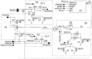
도 4a를 참조하면, 본 발명의 메모리 디바이스(50)에서 사용하기 위한, X디코더(200)의 회로 다이어그램의 일례가 도시되어 있다. X디코더 회로(200)는 선택된 및 비선택된 메모리 셀들(10)의 워드 라인들(22)에 공급될 디코딩된 어드레스 신호들을 제공한다. X디코더 회로(200)는 다음과 같은 방식으로 동작한다. NAND 게이트(201) 및 INV(202)는 (메모리 섹터(sector) (어드레스) 선택으로 지칭되는) 워드 라인(행)의 사전디코딩된 신호 XPA-XPC를 디코딩하는 데 사용된다. 회로(280)는 프리-드라이버(pre-driver)와 (워드 라인) 드라이버로 구성된다. PMOS 트랜지스터들(210, 211) 및 NMOS 트랜지스터(212)는 사전디코딩된 XPZ<0:7>과 조합되는 워드 라인 프리-드라이버이다. 사전디코딩된 신호들 XPZ<0:7>은 (= '0'으로 되어) 8개 중 하나의 행을 선택하는 데 이용된다. PMOS 트랜지스터(213) 및 NMOS 트랜지스터(214)는 하나의 행에 전형적으로 2048 또는 4096개의 셀들을 포함하고 따라서 워드 라인 RC 지연을 위해 사이즈가 큰, 즉 W = 트랜지스터 폭이고 L = 트랜지스터 길이일 때 W/L 비가 큰, 트랜지스터가 필요한 메모리 행을 구동하는 데 사용되는 워드 라인 WL 드라이버이다. 회로(280)는 8회 반복되고, NAND(201) 및 INV(202)는 메모리 섹터 크기 당 8개 행들에 대해 1회씩 반복된다. 전형적으로, 트랜지스터(214)의 소스는 선택해제 상태를 위해 접지 노드(즉, 0 V)에 접속되는데, 여기서 이것은 노드 NWLLOW(240)에 접속된다. 트랜지스터(213)의 소스는 노드 ZVDD(220)에 접속되는데, 이는 판독 동작에서의 Vwlrd(판독 워드 라인 전압)와 동일하고, Vpwl(프로그래밍 동작에서의 프로그래밍 워드 라인 전압)과 동일하다. 프로그래밍 상태에 있어서, 선택된 워드 라인에 대해, 예를 들어 WL = ZVDD = Vpwl = 1.0 V이고, 비선택된 워드 라인에 대해 WL들 = NWLLOW인데, 이는 -0.5 V와 동일하다. 소거 상태에 있어서, 일 실시예에서, 선택된 워드 라인 WL 및 비선택된 워드 라인에 대해, WL들 = NWLLOW = -0.5 V이다. 판독 상태에 있어서, 선택된 워드 라인에 대해, 예를 들어 WL = ZVDD = Vwlrd = 2 V이고, 비선택된 워드 라인들에 대해 WL들 = NWLLOW이며, 이는 일 실시예에서 -0.5 V와 동일하다. 워드 라인 선택해제 라인들(250)은 프로그래밍 동안 특정 워드 라인들을 선택해제하는 데 사용될 수 있다. NMOS 네이티브 고전압(HV) 트랜지스터(290 내지 297)는 절연 트랜지스터로서의 역할을 하여, 저전압 트랜지스터들(213, 214) 상의 전압에서 소거 고전압을 절연시킨다. 그들은 또한 판독 및 프로그래밍 동작에서 통과 게이트로서의 역할을 한다. WLISO 라인(299)은 트랜지스터들(290 내지 267)의 게이트에 대한 제어 바이어스로서, 소거 동안 로우, 예컨대 1 V가 되고 판독 및 프로그래밍 동안 하이, 예컨대 3 내지 5 V가 된다.Referring to FIG. 4A, an example of a circuit diagram of an
도 4b를 참조하면, 워드 라인(22)에 공급되는 네거티브 전압을 발생시키는 (네거티브 및 포지티브 전압들 양측 모두를 제공하는 전하 펌프(56)의 일부인) 네거티브 전하 펌프 발생기(260)의 회로 다이어그램의 일례가 도시되어 있다. 네거티브 전하 펌프 회로(260)는 다음과 같은 방식으로 동작한다. 제1 기간에, PMOS 트랜지스터(263) 및 NMOS 트랜지스터(266)는 커패시터(265)의 (+) 단자(268) 및 (-) 단자(269)를 포지티브 바이어스 전압 NBIAS(267) 및 접지 레벨(즉, 0 V)로 각각 대전시키는 데 사용된다. 제1 기간 이후 다음 기간에, 커패시터(265)의 (+) 단자(268)를 바이어스 레벨(268)로부터 접지 레벨로 방전하기 위해 트랜지스터(266)는 턴오프되고 NMOS 트랜지스터(264)는 턴온된다. 이때, 커패시터(265)의 (-) 단자(269)는 노드 NWLLOW(240)에서의 용량성 부하(capacitive loading)에 대한 커패시터(265)의 값에 따라 네거티브 레벨, 예컨대 -0.5 V에 용량성으로 커플링될 것이다. NBIAS(267)의 레벨 및 커패시터(265)의 값을 조정함으로써, 네거티브 레벨이 조정된다. 메모리 디바이스(50), 예컨대 싱글 웰(single well) CMOS(N 타입 디바이스들을 위한 P-기판 및 P 타입 디바이스들을 위한 싱글 N 웰)을 형성하기 위해 P 기판 = 0 V(접지됨)를 사용하는 반도체 프로세스의 실시예에 있어서, 네거티브 레벨이 P/N+ 순방향 접합 순방향 바이어스(forward junction forward bias)(~-0.6 V)에서 클램핑(clamping)된다. 잘 알려진 바와 같이, 메모리 디바이스(50)는 트윈 웰(twin well) P-sub CMOS 프로세스로 제조될 수 있으며, 2개의 웰들(P 웰 및 N 웰)이 기판(12)에 구성된다. 기판(12)이 P 타입의 도전성이므로, 기판 내의 제1 P 웰은 N 타입의 디바이스들(NMOS)을 위한 것일 것이고, 제2 N 타입의 웰은 P 타입의 디바이스들(PMOS)을 위한 것일 것이다. 네거티브 전압 전하 펌프 발생기(260) 및 워드 라인 디코더(200)는 기판(12) 내에 트리플 웰(triple well)로 제조될 수 있다. 이는 앞에서 설명한 트윈 웰 P-sub CMOS 프로세스 대신 트리플 웰 CMOS 프로세스에 의해 제조된다. 그 경우, 네거티브 펌프 발생기(260) 및 워드 라인 디코더(200)는 (기판(12) 내부에 있는 제2 N 타입 웰로 제조되는) 제3 P 타입 웰과 제2 N 타입 웰로 제조될 것이다. 이러한 제3 P 타입 웰에는 이제 소정의 동작 상태들에 있어서 유리한 네거티브 전압이 인가될 수 있다. 트리플 웰을 갖는 메모리 디바이스(50)를 구성하는 것이 더 프로세스 집약적이지만, 트리플 웰 내에 펌프 발생기(260)와 워드 라인 디코더(200)를 갖는 이점은 워드 라인(22)에 인가되는 네거티브 전압이 더 네거티브 상태, 예를 들어, 소거 실시예에서 사용되는 -6.0 V가 될 수 있다는 것이다(즉, P/N+ 접합 순방향 바이어스 ~-0.6 V에 의해 클램핑되지 않을 수 있다). 이 경우, 제3 P 타입 웰의 전압 상태는 P/N+ 접합 순방향 바이어스를 피하기 위해 네거티브, 예컨대 -6.0 V 또는 -8.0 V 또는 -5.6 V일 수 있다. 일 실시예에서, 메모리 셀(10)은 제3 P 타입 웰로 형성될 수 있다.Referring to FIG. 4B, an example of a circuit diagram of a negative charge pump generator 260 (which is part of charge pump 56 providing both negative and positive voltages) to generate a negative voltage supplied to
도 5를 참조하면, 본 발명의 Psub CMOS 프로세스의 메모리 디바이스(50)에서 사용하기 위한, 포지티브/네거티브 레벨 신호들을 위한 고전압 디코딩 회로(300)의 제1 실시예가 도시되어 있다. hv(고전압, 예컨대 12 V) PMOS 트랜지스터들(321, 322), hv NMOS 트랜지스터(323), 및 lv(저전압, 예를 들어, 3 V) 트랜지스터들(324, 325)로 구성된 회로(320)가 소거/프로그래밍/판독 동작을 위한 WL 신호를 디코딩하는 데 사용된다. 소거 및/또는 프로그래밍에서 전류를 제한하기 위해 (HV 전하 펌프로부터 감소하는 전류를 제한하기 위해) 트랜지스터(322)(WL 전류 리미터(limiter))가 사용된다. 회로(310)는 도 3a에 도시된 바와 같이 소거 또는 프로그래밍 시퀀스의 시작에서 WL 신호가 일단 어써팅(assert)되면(~Vdd) 선택되는 섹터(8개의 행마다 1개의 섹터)에 대한 hv 제어가 가능하도록 하기 위해 사용되는 hv 래치 회로(latch circuit)이다. 섹터가 (사용되지 않을) 불량 섹터인 경우, 네이티브(native) hv NMOS 트랜지스터(351), 인버터(352), NAND(353), lv 래치(인버터(354, 355), 셋(set) lv NMOS 트랜지스터들(356, 359, 358) 및 리셋(reset) lv NMOS 트랜지스터(357)로 구성됨)로 구성된 회로(350)가 hv 신호를 디스에이블(disable)하기 위해 사용된다. lv PMOS 트랜지스터들(331, 332) 및 hv PMOS 트랜지스터(333)로 구성된 회로(330)가 대기 상태 및 판독에서 CG 바이어스 레벨을 제공하는 데 사용된다. 트랜지스터(331)(그의 게이트가 바이어스 레벨에 있음)는, 예를 들어 대기 상태에서, 불량 CG 단자로부터의 전류를 제한하기 위해 CG 단자에 대한 전류 리미터로 동작한다. hv PMOS 트랜지스터들(341, 342)로 구성된 회로(340)가 소거/프로그래밍에서 CG 바이어스 레벨을 제공하는 데 사용된다. 트랜지스터(341)는 HV 전하 펌프로부터 공급되는 전류를 제한하기 위해 소거/프로그래밍에서 CG 단자에 대한 전류 리미터로 동작할 수 있다. hv PMOS 트랜지스터(361), hv 네이티브 NMOS 트랜지스터(362) 및 lv NMOS 트랜지스터들(363, 364)로 구성된 회로(360)가 CG를 디스에이블하기 위해 사용된다. hv PMOS 트랜지스터(371), hv NMOS 트랜지스터(373) 및 lv NMOS 트랜지스터(372)로 구성된 회로(370)가 소거/프로그래밍/판독 상태에 대한 SL 신호를 인에이블(enable)하기 위해 사용된다. lv NMOS 트랜지스터(372)는 SL을 판독 및 소거에서는 접지까지 끌어 내리고, 프로그래밍에서는 바이어스 레벨, 예를 들어, 2 V 미만으로 끌어 내리는 데 사용된다. 회로(380)는 CG 신호를 위한 네거티브 디코딩 회로이다. 회로(360)는 Psub CMOS 프로세스를 위해 (회로(380)에 의해 제공되어 메모리 셀의 CG 단자로 들어가는) 네거티브 레벨을 NMOS 트랜지스터(362)로부터 절연시키기 위해 PMOS 트랜지스터(361)를 절연 트랜지스터로서 사용한다. 회로(380)는 클럭드 네거티브 부트스트래핑된 고전압 회로 방식(clocked negatively bootstrapped high voltage circuit scheme)을 사용한다. 회로(380)는 PMOS 트랜지스터들(381, 382, 385 내지 391), NOR(384) 및 인버터(384)로 구성된다. NOR(384) 및 인버터(384)는 트랜지스터(387)의 게이트를 네거티브로 펌핑하기 위해 커패시터로서 동작하는 PMOS 트랜지스터들(386, 388)로 클럭킹 신호(clocking signal)를 인에이블하는 데 사용된다. 트랜지스터(385)는 PMOS 트랜지스터(387) 및 PMOS 커패시터들(386, 388)을 위한 부트스트랩 트랜지스터로서 동작한다. 트랜지스터들(381/390, 382/391)은 트랜지스터(387)의 드레인 및 트랜지스터(385)의 드레인을 각각 Vdd 레벨에서 클램핑하는 역할을 한다. 트랜지스터(389)는 CG 내로의 네거티브 레벨을 위한 버퍼로서의 역할을 한다. 트랜지스터들(385, 387)의 소스들은 네거티브 전원 VCGNEG(399)에 접속된다.Referring to FIG. 5, a first embodiment of a high voltage decoding circuit 300 for positive / negative level signals for use in a
도 6을 참조하면, 본 발명의 트리플 웰 CMOS 프로세스의 메모리 디바이스(50)에서 사용하기 위한, 포지티브/네거티브 레벨 신호들을 위한 고전압 디코딩 회로(400)의 제2 실시예가 도시되어 있다. 회로들(310 내지 350, 370)은 도 5의 회로들과 동일하거나 유사하다. hv NMOS 트랜지스터(410)와 lv NMOS 트랜지스터들(412 내지 414)로 구성된 회로(410)가 CG들을 낮은 레벨, 예컨대 0 V로 선택해제하는 데 사용된다. hv 트랜지스터(410)는 CG들 내로의 네거티브 레벨을 절연시키기 위해 절연 트랜지스터로서의 역할을 하여, 따라서 그의 벌크 VCGNEG도 또한 네거티브 레벨에 있다. 네거티브 레벨 시프터(shifter)로서의 역할을 하는 회로(420)가 CG들에 대한 네거티브 레벨을 제공하는 데 사용된다. 회로(420)는 인에이블링 엔티티(entity)로서 NAND(421)와 인버터(422)로, 교차 커플링된 네거티브 래치(cross-coupled negative latch)로서 hv PMOS 트랜지스터들(423, 424)과 hv NMOS 트랜지스터들(425, 426)로, 그리고 버퍼로서 hv NMOS 트랜지스터(427)로 구성된다. NMOS 트랜지스터들(425, 426, 427)의 소스들은 네거티브 전원 VCGNEG에 접속된다.Referring to FIG. 6, a second embodiment of a high voltage decoding circuit 400 for positive / negative level signals for use in a
도 7을 참조하면, 본 발명의 Psub CMOS 프로세스의 메모리 디바이스(50)에서 사용하기 위한, 포지티브/네거티브 레벨 신호들을 위한 고전압 디코딩 회로(420)의 제3 실시예가 도시되어 있다. 네거티브 전압을 위해 다이오드 디코딩 방식을 사용한다. 회로들(310 내지 370)은 도 5의 회로들과 동일하거나 유사하다. hv PMOS 트랜지스터(512)로 구성된 회로(510)가 CG들 내로의 네거티브 레벨을 제공하는 데 사용된다. 트랜지스터(512)는 다이오드 접속된 것으로, 게이트-드레인이 함께 접속됨을 의미하며, 그의 게이트-드레인은 네거티브 전원 VCGNEG에 접속된다. 그의 소스는 CG에 접속된다. 따라서, 네거티브 전원 VCGNEG가 네거티브가 될 때, 트랜지스터의 소스는 VCG NEG - |Vtp|의 양만큼 네거티브가 된다.Referring to FIG. 7, there is shown a third embodiment of a high
도 8을 참조하면, 소거 동작 동안 커플링 게이트(26)에 인가되는 네거티브 전압들을 발생시키는 네거티브 전하 펌프(600)가 도시되어 있다. PMOS 트랜지스터들(612, 613)과 커패시터들(611, 614)로 구성되는 회로(610)가 펌프 스테이지를 구성한다. 트랜지스터(613)는 (전하를 한 스테이지에서 다음 스테이지로 전달하는) 트랜스퍼 트랜지스터이다. 트랜지스터(612)와 커패시터(611)는 트랜스퍼 트랜지스터(613)를 위한 Vt-캔슬링(cancelling) 기능으로서의 역할을 한다. 커패시터(614)는 (펌핑 전하를 제공한다는 의미의) 펌핑 커패시터이다. 다이오드 접속 PMOS 트랜지스터(620)가 제1 펌프 스테이지에 대한 전원 노드에 접속된다. 다이오드 접속 PMOS 트랜지스터(640)가 마지막 펌프 스테이지로부터 출력 전하 펌프 노드에 접속하는 역할을 한다. PMOS 트랜지스터들(650, 652)은 내부의 펌핑된 노드들을 클램핑하거나 초기화하는 역할을 한다. 다양한 클럭 발생, 페이즈 드라이버(phase driver) 및 바이어스들은 도시되지 않는다.Referring to FIG. 8, there is shown a negative charge pump 600 that generates negative voltages applied to the
도 9를 참조하면, 본 발명의 메모리 디바이스(50)에서 사용하기 위한, 네거티브 고전압 조정 회로(700)의 일 실시예가 도시되어 있다. 커패시터들(702, 704)은 네거티브 전원 VCGNEG(399)로부터의 네거티브 전압을 기준 전압 VREF(708), 즉 1 V와 비교되는 전압으로 분할하는 데 사용된다. VREF(708)는 비교기(710)의 단자와 연결된다. 노드(706)를 바이어스 전압, 예를 들어, 2 V로 초기화시키기 위해 트랜지스터(714)가 사용된다. 노드(706)는 비교기(710)의 다른 단자와 연결된다. 네거티브 전원 VCGNEG(399)가 접지와 같은 레벨로부터 점차적으로 네거티브로 펌핑되면, 노드(706)는 비례적으로 바이어스 레벨, 예컨대 포지티브 2 V로부터 네거티브 방향으로 (커패시터들(702, 704)의 값들에 의해 결정되는 비로) 점차 낮아진다. 일단 노드(706)가 VREF(708)와 동일한 값에 도달하면, 비교기(710)는 극성을 전환한다. 이어서, 출력 REGOUT(718)는 네거티브 전원 VCGNMEG(399)가 소거 상태에서 CG를 위해 사용되는 -9 V와 같은 원하는 레벨에 도달하였다는 신호를 보내기 위해 사용된다.Referring to FIG. 9, an embodiment of a negative high voltage regulation circuit 700 for use in the
도 10을 참조하면, 본 발명의 Psub CMOS 프로세스의 메모리 디바이스(50)에서 사용하기 위한, 네거티브 테스트 패드 회로(800)의 일 실시예가 도시되어 있다. PMOS 트랜지스터(810)는 내부 패드로부터 외부 패드로 또는 그 역으로 전달되도록 NMOS 트랜지스터(812)를 네거티브 레벨로 절연시키는 역할을 한다. 트랜지스터(810)는 절연을 위해 그의 드레인에 접속된 그의 벌크를 갖는다. 트랜지스터(812)는 ESD 클램핑으로서 역할을 한다.Referring to FIG. 10, one embodiment of a negative
도 11a 및 도 11b를 참조하면, 종래 기술의 포지티브 고전압 동작을 갖는 메모리 셀들을 생산하기 위한 종래 기술 실시예들의 프로세스 흐름 단면도(900, 901)가 도시되어 있다. 메모리 셀은 CG 폴리(poly) 층(904), ONO 층(905), FG 폴리 층(906), SL 폴리 층(908), SL 확산 층(912), FG 게이트 산화물 층(914), 및 WL 폴리 층(955)을 포함한다. 프로세스 흐름 단면도(900)에서, 주변 HV 디바이스는 게이트 폴리(982), 게이트 폴리 하부의 채널 영역(988), LDD(LDD 주입)(980)를 포함한다. 이 경우, 주변 HV 게이트 폴리(982)는 두꺼워서 LDD 주입(980)이 채널 영역(988) 내로 들어가는 것을 막을 수 있다. 개선된 더 작은 기하학적 기술 노드(geometry technology node)에 적용가능한 프로세스 흐름 단면(901)의 경우에, 메모리 셀은 WL 폴리(965)를 포함하고, 주변 HV 디바이스는 게이트 폴리(984), 기판(988), LDD(LDD 주입)(980)를 포함한다. 게이트 폴리(984)는 게이트 폴리(982)보다 상당히 얇다. 이 경우, LDD 주입(980)은 게이트 폴리(984)를 관통하여 채널(988)을 전기적으로 변조하는 채널 영역(988)으로 들어간다. 이러한 결과는 바람직하지 않다. 이 경우, LDD 주입이 채널 내부로 관통하는 것을 중단시키기 위해 추가적인 마스킹 및/또는 프로세스 층 단계가 필요할 수 있다.Referring to Figures 11A and 11B, process flow
도 11c를 참조하면, 본 발명의 메모리 디바이스(50)에서 사용하기 위한, 네거티브 전압 동작을 갖는 메모리 셀들(10)의 생산을 위한 프로세스 흐름의 일 실시예가 도시되어 있다. 이 경우, LDD 주입(981)은, 예컨대 네거티브 전압 동작에 대해 9 V 대 11 V인, 더 낮은 고전압 요구사항으로 인해 에너지가 상당히 더 낮다. 따라서, 이 경우, 더 작은 기하학적 기술 노드와 얇은 게이트 폴리(984) 두께를 갖더라도 LDD 주입이 채널(988)로 관통하여 들어가지 않는다. 따라서, 이 프로세스 흐름은 네거티브 전압 동작과 함께 사용하기 위한 메모리 셀을 생산하는 데 적합하다.Referring to FIG. 11C, one embodiment of a process flow for the production of
판독, 소거 및 프로그래밍의 동작들 동안 네거티브 전압을 비선택된 또는 선택된 메모리 셀들(10)의 워드 라인(22)에 적용하는 것의 이점은 메모리 셀이 더욱 효과적으로 스케일을 낮추도록 허용하는 것이다. 소거 동안, 선택된 메모리 셀들의 워드 라인 상의 네거티브 전압은 전체적인 소거 전압이 낮아지는 것을 허용하여 따라서 셀의 치수가 더 작아지도록 허용한다(다양한 셀간(inter-cell) 또는 층간(inter-layer) 치수인 수평 또는 수직 간격, 절연, 폭, 길이 등에 걸쳐서 더 낮은 전압을 유지함). 프로그래밍 동안, 비선택된 메모리 셀들의 워드 라인 상의 네거티브 전압은 비선택된 메모리 셀들에 대한 누설을 감소시켜서 (동일 섹터 내의 비선택된 셀들에 대해) 더 적은 교란, 더 정확한 프로그래밍 전류(선택된 셀들에 대해, 더 적은 누설 간섭), 및 더 적은 전력 소비로 이어진다. 판독의 경우에, 비선택된 메모리 셀들의 워드 라인 상의 네거티브 전압은 누설로부터의 더 적은 간섭으로 인해 더욱 정확한 감지로 이어진다. 메모리 어레이 동작에서 사용하기 위해 네거티브 워드 라인, 네거티브 커플링 게이트 및 네거티브 P 기판을 조합하면, 낮아진 소거/프로그래밍 전압들 및 전류, 더욱 효과적인 소거 및 프로그래밍, 더 적은 셀 교란, 더 적은 셀 누설의 결과를 가져온다는 것이 또한 유리하다.The advantage of applying a negative voltage to the word lines 22 of unselected or selected
Claims (40)
제1 도전성 타입의 반도체 기판; 및
복수의 행(row)들 및 열(column)들로 배열된 상기 반도체 기판 내의 비휘발성 메모리 셀들의 어레이를 포함하고, 각각의 메모리 셀은,
제2 도전성 타입의, 상기 반도체 기판의 표면 상의 제1 영역;
상기 제2 도전성 타입의, 상기 반도체 기판의 표면 상의 제2 영역;
상기 제1 영역과 상기 제2 영역 사이의 채널 영역;
상기 채널 영역의 제1 부분 위에 놓여 있고 그로부터 절연되며, 상기 제1 영역에 인접하고 상기 제1 영역과 거의 또는 전혀 중첩되지 않는 워드 라인;
상기 채널 영역의 제2 부분 위에 놓여 있고, 상기 제1 부분에 인접하고, 그로부터 절연되고 상기 제2 영역에 인접한 플로팅 게이트;
상기 플로팅 게이트 위에 놓인 커플링 게이트;
상기 제1 영역에 접속된 비트 라인;
제1 네거티브 전압을 생성하기 위한 네거티브 전하 펌프 회로; 및
커맨드 신호를 수신하고, 이에 응답하여, 복수의 제어 신호들을 생성하여 선택된 메모리 셀들의 커플링 게이트에 대한 상기 제1 네거티브 전압의 인가를 제어하기 위한 제어 회로를 포함하는, 비휘발성 메모리 디바이스.A non-volatile memory device comprising:
A semiconductor substrate of a first conductivity type; And
And an array of non-volatile memory cells in the semiconductor substrate arranged in a plurality of rows and columns,
A first region of a second conductivity type on the surface of the semiconductor substrate;
A second region of the second conductivity type on the surface of the semiconductor substrate;
A channel region between the first region and the second region;
A word line disposed over and insulated from a first portion of the channel region, the word line being adjacent to the first region and having little or no overlap with the first region;
A floating gate overlying a second portion of the channel region, adjacent to the first portion, insulated therefrom and adjacent the second region;
A coupling gate overlying the floating gate;
A bit line connected to the first region;
A negative charge pump circuit for generating a first negative voltage; And
And a control circuit for receiving a command signal and, in response thereto, generating a plurality of control signals to control application of the first negative voltage to a coupling gate of selected memory cells.
상기 복수의 제어 신호들은 소거 커맨드에 응답하여 생성되는, 비휘발성 메모리 디바이스.The method according to claim 1,
Wherein the plurality of control signals are generated in response to an erase command.
상기 네거티브 전하 펌프는 제2 네거티브 전압을 생성하고, 상기 제어 회로는 상기 제2 네거티브 전압을 비선택된 메모리 셀의 워드 라인에 인가하는, 비휘발성 메모리 디바이스.The method of claim 2,
Wherein the negative charge pump generates a second negative voltage and the control circuit applies the second negative voltage to a word line of a non-selected memory cell.
상기 복수의 제어 신호들은 판독 커맨드에 응답하여 셍성되는, 비휘발성 메모리 디바이스.The method according to claim 1,
The plurality of control signals being responsive to a read command.
상기 복수의 제어 신호들은 프로그래밍 커맨드에 응답하여 생성되는, 비휘발성 메모리 디바이스.The method according to claim 1,
Wherein the plurality of control signals are generated in response to a programming command.
상기 네거티브 전하 펌프는 상기 반도체 기판 내의 트리플 웰(triple well)에 있는, 비휘발성 메모리 디바이스.The method according to claim 1,
Wherein the negative charge pump is in a triple well in the semiconductor substrate.
상기 메모리 셀들, 네거티브 전하 펌프, 및 제어 회로는 트윈 웰(twin well) P-sub CMOS 프로세스에서 제공되는 반도체 P 기판에 형성되는, 비휘발성 메모리 디바이스.The method according to claim 1,
Wherein the memory cells, the negative charge pump, and the control circuit are formed in a semiconductor P substrate provided in a twin well P-sub CMOS process.
상기 제어 회로는 네거티브 전압 다이오드-디코딩 회로를 포함하는, 비휘발성 메모리 디바이스.The method according to claim 1,
Wherein the control circuit comprises a negative voltage diode-decoding circuit.
상기 제어 회로는 네거티브 레벨 시프터 회로(negative level shifter circuit) 및 클럭드 네거티브 부트스트래핑 회로(clocked negative bootstrapping circuit)를 포함하는, 비휘발성 메모리 디바이스.The method according to claim 1,
Wherein the control circuit comprises a negative level shifter circuit and a clocked negative bootstrapping circuit. ≪ Desc / Clms Page number 13 >
고전압 PMOS 트랜지스터와 고전압 NMOS 트랜지스터를 포함하는 네거티브 테스트 패드 회로(negative test pad circuit)를 추가로 포함하는, 비휘발성 메모리 디바이스.The method according to claim 1,
Further comprising a negative test pad circuit comprising a high voltage PMOS transistor and a high voltage NMOS transistor.
커패시터-디바이더(divider) 기반의 비교기를 갖는 네거티브 조정 회로(negative regulation circuit)를 추가로 포함하는, 비휘발성 메모리 디바이스.The method according to claim 1,
Further comprising a negative regulation circuit having a capacitor-divider based comparator. ≪ RTI ID = 0.0 > A < / RTI >
상기 제어 회로는 상기 메모리 셀들에 포지티브(positive) 또는 네거티브 고전압을 공급하기 위해 고전압 디코더에 전류 리미터(current limiter)를 포함하는, 비휘발성 메모리 디바이스.The method according to claim 1,
Wherein the control circuit includes a current limiter in the high voltage decoder to supply a positive or negative high voltage to the memory cells.
상기 제어 회로는 상기 메모리 셀들에 상기 워드 라인 상의 소거 전압을 공급하기 위해 고전압 디코더에 전류 리미터를 포함하는, 비휘발성 메모리 디바이스.The method according to claim 1,
Wherein the control circuit includes a current limiter in the high voltage decoder to supply an erase voltage on the word line to the memory cells.
상기 제어 회로는 상기 메모리 셀들의 커플링 게이트 상에 전압을 공급하기 위해 고전압 디코더에 전류 리미터를 포함하는, 비휘발성 메모리 디바이스.The method according to claim 1,
Wherein the control circuit includes a current limiter in the high voltage decoder to supply a voltage on the coupling gate of the memory cells.
상기 제어 회로는 프로그래밍 또는 소거 동작 동안 상기 메모리 셀들의 커플링 게이트 상에 전압을 공급하기 위해 고전압 디코더에 전류 리미터를 포함하는, 비휘발성 메모리 디바이스.15. The method of claim 14,
Wherein the control circuit includes a current limiter in the high voltage decoder to supply a voltage on the coupling gate of the memory cells during a programming or erasing operation.
상기 제어 회로는 프로그래밍 또는 소거 또는 판독 동작에서 상기 메모리 셀들에 전압들을 공급하기 위해 고전압 디코더에 고전압 래치를 포함하는, 비휘발성 메모리 디바이스.The method according to claim 1,
Wherein the control circuit comprises a high voltage latch in the high voltage decoder to supply voltages to the memory cells in a programming or erasing or reading operation.
상기 제어 회로는 프로그래밍 또는 소거 또는 판독 동작에서 상기 메모리 셀들에 전압들을 공급하기 위해 고전압 디코더에 고전압 레벨 시프터를 포함하는, 비휘발성 메모리 디바이스.The method according to claim 1,
Wherein the control circuit comprises a high voltage level shifter in the high voltage decoder to supply voltages to the memory cells in a programming or erasing or reading operation.
상기 제어 회로는 프로그래밍 또는 소거 또는 판독 동작에서 상기 메모리 셀들에 전압들을 공급하기 위해 고전압 디코더에 저전압 래치를 포함하는, 비휘발성 메모리 디바이스.The method according to claim 1,
Wherein the control circuit comprises a low voltage latch in the high voltage decoder to supply voltages to the memory cells in a programming or erasing or reading operation.
프로그래밍 또는 소거 또는 판독 동작에서 상기 메모리 셀들에 전압들을 공급하기 위한 저전압 디코더를 추가로 포함하는, 비휘발성 메모리 디바이스.The method according to claim 1,
Further comprising a low voltage decoder for supplying voltages to the memory cells in a programming or erasing or reading operation.
상기 저전압 디코더는 프로그래밍, 소거, 또는 판독 동작에서 상기 메모리 셀들에 전압들을 공급하기 위한 워드 라인 드라이버에 절연 트랜지스터를 포함하는, 비휘발성 메모리 디바이스.The method of claim 19,
Wherein the low voltage decoder comprises an isolation transistor in a word line driver for supplying voltages to the memory cells in a programming, erasing, or reading operation.
각각의 메모리 셀은 분리형 게이트 플래시 메모리 셀인, 비휘발성 메모리 디바이스.The method according to claim 1,
Each memory cell being a removable gate flash memory cell.
각각의 메모리 셀은 팁 소거(tip erasing)를 갖는 분리형 게이트 플래시 메모리 셀인, 비휘발성 메모리 디바이스.The method of claim 20,
Each memory cell being a removable gate flash memory cell with tip erasing.
각각의 메모리 셀은 상기 워드 라인으로부터 플로팅 게이트로의 팁 소거를 갖는 분리형 게이트 플래시 메모리 셀인, 비휘발성 메모리 디바이스.The method of claim 20,
Each memory cell being a removable gate flash memory cell having a tip erase from the word line to a floating gate.
상기 비휘발성 메모리 디바이스는,
제1 도전성 타입의 반도체 기판; 및 복수의 행들 및 열들로 배열된 상기 반도체 기판 내의 비휘발성 메모리 셀들의 어레이를 갖고, 각각의 메모리 셀은, 제2 도전성 타입의, 상기 반도체 기판의 표면 상의 제1 영역; 상기 제2 도전성 타입의, 상기 반도체 기판의 표면 상의 제2 영역; 상기 제1 영역과 상기 제2 영역 사이의 채널 영역; 상기 채널 영역의 제1 부분 위에 놓여 있고 그로부터 절연되며, 상기 제1 영역에 인접하고 상기 제1 영역과 거의 또는 전혀 중첩되지 않는 워드 라인; 상기 채널 영역의 제2 부분 위에 놓여 있고, 상기 제1 부분에 인접하고, 그로부터 절연되고, 상기 제2 영역에 인접한 플로팅 게이트; 상기 플로팅 게이트 위에 놓인 커플링 게이트; 및 상기 제1 영역에 접속된 비트 라인을 갖고, 상기 방법은,
제1 네거티브 전압을 선택된 메모리 셀들의 상기 커플링 게이트에 인가하는 단계; 및
비네거티브 전압(non-negative voltage)을 상기 선택된 메모리 셀의 상기 워드 라인, 상기 비트 라인, 및 상기 제2 영역에 인가하는 단계를 포함하는, 방법.A method of operating a certain type of non-volatile memory device,
The nonvolatile memory device comprising:
A semiconductor substrate of a first conductivity type; And an array of non-volatile memory cells in the semiconductor substrate arranged in a plurality of rows and columns, each memory cell comprising: a first region of a second conductivity type on a surface of the semiconductor substrate; A second region of the second conductivity type on the surface of the semiconductor substrate; A channel region between the first region and the second region; A word line disposed over and insulated from a first portion of the channel region, the word line being adjacent to the first region and having little or no overlap with the first region; A floating gate overlying a second portion of the channel region, adjacent to the first portion, insulated therefrom and adjacent the second region; A coupling gate overlying the floating gate; And a bit line connected to the first region,
Applying a first negative voltage to the coupling gate of selected memory cells; And
Applying a non-negative voltage to the word line, the bit line, and the second region of the selected memory cell.
상기 방법은 상기 선택된 메모리 셀을 소거하기 위한 것인, 방법.27. The method of claim 24,
The method is for erasing the selected memory cell.
0(zero) 전압이 상기 선택된 메모리 셀의 상기 비트 라인 및 제2 영역에 인가되고, 포지티브 전압이 상기 선택된 메모리 셀의 상기 워드 라인에 인가되는, 방법.26. The method of claim 25,
A zero voltage is applied to the bit line and the second region of the selected memory cell and a positive voltage is applied to the word line of the selected memory cell.
다른 전압들이 상기 선택된 메모리 셀들의 상기 워드 라인 제2 영역에 인가되기 전에 상기 네거티브 전압이 상기 커플링 게이트에 인가되는, 방법.27. The method of claim 26,
Wherein the negative voltage is applied to the coupling gate before other voltages are applied to the word line second region of the selected memory cells.
상기 선택된 메모리 셀들의 상기 커플링 게이트에 인가되는 상기 전압은 네거티브 전압인, 방법.27. The method of claim 24,
Wherein the voltage applied to the coupling gate of the selected memory cells is a negative voltage.
상기 방법은 상기 선택된 메모리 셀을 판독하기 위한 것인, 방법.27. The method of claim 24,
Wherein the method is for reading the selected memory cell.
상기 방법은 상기 선택된 메모리 셀을 프로그래밍하기 위한 것인, 방법.27. The method of claim 24,
Wherein the method is for programming the selected memory cell.
상기 방법은 소스측 주입에 의해 상기 선택된 메모리 셀을 프로그래밍하기 위한 것인, 방법.32. The method of claim 30,
Wherein the method is for programming the selected memory cell by source side injection.
비네거티브 전압을 상기 선택된 메모리 셀의 상기 워드 라인, 비트 라인, 커플링 게이트, 및 제2 영역에 인가하는 상기 방법은 오직 판독 및 프로그래밍의 동작만을 위한 것인, 방법.27. The method of claim 24,
Wherein the method of applying a non-negative voltage to the word line, bit line, coupling gate, and second region of the selected memory cell is for read and programming operations only.
상기 방법은
소거 동작 동안 네거티브 전압을 비선택된 메모리 셀의 상기 커플링 게이트에 인가하는 단계를 추가로 포함하는, 방법.33. The method of claim 32,
The method
Further comprising applying a negative voltage to the coupling gate of a non-selected memory cell during an erase operation.
상기 방법은
프로그래밍 동작 동안 제2 네거티브 전압을 상기 선택된 메모리 셀의 상기 제2 영역에 인가하는 단계를 추가로 포함하는, 방법.32. The method of claim 30,
The method
Further comprising applying a second negative voltage to the second region of the selected memory cell during a programming operation.
상기 제2 네거티브 전압은 상기 제1 네거티브 전압과 상이한, 방법.34. The method of claim 33,
Wherein the second negative voltage is different from the first negative voltage.
상기 프로그래밍 동안, 상기 전압은 상기 전압이 상기 선택된 메모리 셀들의 상기 제2 영역에 인가된 후에 상기 커플링 게이트에 인가되는, 방법.33. The method of claim 32,
During the programming, the voltage is applied to the coupling gate after the voltage is applied to the second region of the selected memory cells.
상기 판독 동안, 상기 커플링 게이트에 인가되는 상기 전압은 상기 전압이 상기 선택된 메모리 셀들의 상기 워드 라인과 비트 라인에 인가되기 전에 인가되는, 방법.26. The method of claim 25,
During which the voltage applied to the coupling gate is applied before the voltage is applied to the word line and the bit line of the selected memory cells.
터널링(tunneling)은 상기 워드 라인으로부터 상기 플로팅 게이트까지인, 방법.26. The method of claim 25,
Wherein tunneling is from the word line to the floating gate.
상기 터널링은 워드라인 아크 영역으로부터 상기 플로팅 게이트까지인, 방법.42. The method of claim 38,
Wherein the tunneling is from the word line arc region to the floating gate.
상기 터널링은 상기 워드 라인으로부터 플로팅 게이트 팁 코너까지인, 방법.42. The method of claim 38,
Wherein the tunneling is from the word line to the floating gate tip corner.
Applications Claiming Priority (3)
| Application Number | Priority Date | Filing Date | Title |
|---|---|---|---|
| US14/506,433 | 2014-10-03 | ||
| US14/506,433 US9922715B2 (en) | 2014-10-03 | 2014-10-03 | Non-volatile split gate memory device and a method of operating same |
| PCT/US2015/050010 WO2016053607A1 (en) | 2014-10-03 | 2015-09-14 | A non-volatile split gate memory device and a method of operating same |
Publications (2)
| Publication Number | Publication Date |
|---|---|
| KR20170061160A true KR20170061160A (en) | 2017-06-02 |
| KR101982948B1 KR101982948B1 (en) | 2019-08-28 |
Family
ID=54200098
Family Applications (1)
| Application Number | Title | Priority Date | Filing Date |
|---|---|---|---|
| KR1020177011636A KR101982948B1 (en) | 2014-10-03 | 2015-09-14 | A non-volatile split gate memory device and a method of operating same |
Country Status (7)
| Country | Link |
|---|---|
| US (2) | US9922715B2 (en) |
| EP (1) | EP3201926A1 (en) |
| JP (1) | JP6486462B2 (en) |
| KR (1) | KR101982948B1 (en) |
| CN (1) | CN107077891B (en) |
| TW (1) | TWI641113B (en) |
| WO (1) | WO2016053607A1 (en) |
Cited By (1)
| Publication number | Priority date | Publication date | Assignee | Title |
|---|---|---|---|---|
| KR20200024310A (en) * | 2017-08-25 | 2020-03-06 | 실리콘 스토리지 테크놀로지 인크 | Improved sense amplifier circuit for reading data from flash memory cells |
Families Citing this family (8)
| Publication number | Priority date | Publication date | Assignee | Title |
|---|---|---|---|---|
| US20160005749A1 (en) * | 2014-07-01 | 2016-01-07 | Qualcomm Incorporated | Series ferroelectric negative capacitor for multiple time programmable (mtp) devices |
| US9953719B2 (en) * | 2016-05-18 | 2018-04-24 | Silicon Storage Technology, Inc. | Flash memory cell and associated decoders |
| JP2019067474A (en) * | 2017-10-05 | 2019-04-25 | 東芝メモリ株式会社 | Semiconductor memory device |
| US11354562B2 (en) * | 2018-01-03 | 2022-06-07 | Silicon Storage Technology, Inc. | Programmable neuron for analog non-volatile memory in deep learning artificial neural network |
| US10847225B2 (en) * | 2018-06-20 | 2020-11-24 | Microchip Technology Incorporated | Split-gate flash memory cell with improved read performance |
| US11081184B2 (en) | 2019-10-30 | 2021-08-03 | Sandisk Technologies Llc | Method of concurrent multi-state programming of non-volatile memory with bit line voltage step up |
| US20210134369A1 (en) * | 2019-10-30 | 2021-05-06 | Sandisk Technologies Llc | Method for concurrent programming |
| CN114335186A (en) * | 2020-09-30 | 2022-04-12 | 硅存储技术股份有限公司 | Split-gate non-volatile memory cell with erase gate disposed over word line gate and method of making the same |
Citations (4)
| Publication number | Priority date | Publication date | Assignee | Title |
|---|---|---|---|---|
| US20070070703A1 (en) * | 2005-09-26 | 2007-03-29 | Tran Hieu V | Flash memory array system including a top gate memory cell |
| US20100127308A1 (en) * | 2008-11-26 | 2010-05-27 | Nhan Do | Non-volatile memory cell with self aligned floating and erase gates, and method of making same |
| US20130242672A1 (en) * | 2012-03-13 | 2013-09-19 | Silicon Storage Technology, Inc. | Non-volatile Memory Device And A Method Of Operating Same |
| WO2014172433A1 (en) * | 2013-04-16 | 2014-10-23 | Silicon Storage Technology, Inc. | Non-volatile memory cell with self aligned floating and erase gates, and method of making same |
Family Cites Families (12)
| Publication number | Priority date | Publication date | Assignee | Title |
|---|---|---|---|---|
| KR19990088517A (en) * | 1998-05-22 | 1999-12-27 | 마 유에 예일 | A nonvolatile memory cell structure and method for operating nonvolatile memory cells |
| TW546840B (en) * | 2001-07-27 | 2003-08-11 | Hitachi Ltd | Non-volatile semiconductor memory device |
| DE10361718A1 (en) * | 2003-08-22 | 2005-03-17 | Hynix Semiconductor Inc., Ichon | Apparatus and method for controlling nonvolatile DRAM |
| US7145802B2 (en) | 2004-08-31 | 2006-12-05 | Skymedi Corporation | Programming and manufacturing method for split gate memory cell |
| JP2007207380A (en) * | 2006-02-03 | 2007-08-16 | Renesas Technology Corp | Nonvolatile semiconductor memory device |
| US8138524B2 (en) * | 2006-11-01 | 2012-03-20 | Silicon Storage Technology, Inc. | Self-aligned method of forming a semiconductor memory array of floating memory cells with source side erase, and a memory array made thereby |
| JP2008287794A (en) * | 2007-05-17 | 2008-11-27 | Renesas Technology Corp | Semiconductor integrated circuit and operating method thereof |
| US8488388B2 (en) * | 2011-11-01 | 2013-07-16 | Silicon Storage Technology, Inc. | Method of programming a split gate non-volatile floating gate memory cell having a separate erase gate |
| US8804429B2 (en) * | 2011-12-08 | 2014-08-12 | Silicon Storage Technology, Inc. | Non-volatile memory device and a method of programming such device |
| US9472284B2 (en) * | 2012-11-19 | 2016-10-18 | Silicon Storage Technology, Inc. | Three-dimensional flash memory system |
| US9418744B2 (en) * | 2014-05-12 | 2016-08-16 | Silicon Storage Technology, Inc. | System and method to reduce disturbances during programming of flash memory cells |
| CN105609131A (en) * | 2014-07-22 | 2016-05-25 | 硅存储技术公司 | System and method for inhibiting erasing of part of splitting gate flash memory unit sector |
-
2014
- 2014-10-03 US US14/506,433 patent/US9922715B2/en active Active
-
2015
- 2015-09-14 EP EP15771380.1A patent/EP3201926A1/en not_active Ceased
- 2015-09-14 CN CN201580053591.1A patent/CN107077891B/en active Active
- 2015-09-14 WO PCT/US2015/050010 patent/WO2016053607A1/en active Application Filing
- 2015-09-14 KR KR1020177011636A patent/KR101982948B1/en active IP Right Grant
- 2015-09-14 JP JP2017518062A patent/JP6486462B2/en active Active
- 2015-09-23 TW TW104131431A patent/TWI641113B/en active
-
2016
- 2016-03-30 US US15/085,835 patent/US20160217864A1/en not_active Abandoned
Patent Citations (4)
| Publication number | Priority date | Publication date | Assignee | Title |
|---|---|---|---|---|
| US20070070703A1 (en) * | 2005-09-26 | 2007-03-29 | Tran Hieu V | Flash memory array system including a top gate memory cell |
| US20100127308A1 (en) * | 2008-11-26 | 2010-05-27 | Nhan Do | Non-volatile memory cell with self aligned floating and erase gates, and method of making same |
| US20130242672A1 (en) * | 2012-03-13 | 2013-09-19 | Silicon Storage Technology, Inc. | Non-volatile Memory Device And A Method Of Operating Same |
| WO2014172433A1 (en) * | 2013-04-16 | 2014-10-23 | Silicon Storage Technology, Inc. | Non-volatile memory cell with self aligned floating and erase gates, and method of making same |
Cited By (1)
| Publication number | Priority date | Publication date | Assignee | Title |
|---|---|---|---|---|
| KR20200024310A (en) * | 2017-08-25 | 2020-03-06 | 실리콘 스토리지 테크놀로지 인크 | Improved sense amplifier circuit for reading data from flash memory cells |
Also Published As
| Publication number | Publication date |
|---|---|
| WO2016053607A1 (en) | 2016-04-07 |
| CN107077891A (en) | 2017-08-18 |
| EP3201926A1 (en) | 2017-08-09 |
| KR101982948B1 (en) | 2019-08-28 |
| TW201618285A (en) | 2016-05-16 |
| CN107077891B (en) | 2021-03-30 |
| US20160217864A1 (en) | 2016-07-28 |
| US20160099067A1 (en) | 2016-04-07 |
| JP2017531896A (en) | 2017-10-26 |
| JP6486462B2 (en) | 2019-03-20 |
| US9922715B2 (en) | 2018-03-20 |
| TWI641113B (en) | 2018-11-11 |
Similar Documents
| Publication | Publication Date | Title |
|---|---|---|
| US10325666B2 (en) | Flash memory system using negative high voltage level shifter | |
| KR101982948B1 (en) | A non-volatile split gate memory device and a method of operating same | |
| KR101538284B1 (en) | A non-volatile memory device and a method of operating same | |
| KR20190002711A (en) | An improved flash memory cell and associated decoders | |
| KR20180042421A (en) | Flash memory system using dummy memory cells as source line pull-down circuits |
Legal Events
| Date | Code | Title | Description |
|---|---|---|---|
| A201 | Request for examination | ||
| E902 | Notification of reason for refusal | ||
| E701 | Decision to grant or registration of patent right | ||
| GRNT | Written decision to grant |