KR20170014558A - Light emitting diode(LED) package - Google Patents
Light emitting diode(LED) package Download PDFInfo
- Publication number
- KR20170014558A KR20170014558A KR1020150108148A KR20150108148A KR20170014558A KR 20170014558 A KR20170014558 A KR 20170014558A KR 1020150108148 A KR1020150108148 A KR 1020150108148A KR 20150108148 A KR20150108148 A KR 20150108148A KR 20170014558 A KR20170014558 A KR 20170014558A
- Authority
- KR
- South Korea
- Prior art keywords
- electrode
- light emitting
- layer
- molding resin
- pad
- Prior art date
Links
- 239000011347 resin Substances 0.000 claims abstract description 167
- 229920005989 resin Polymers 0.000 claims abstract description 167
- 238000000465 moulding Methods 0.000 claims abstract description 164
- 239000004065 semiconductor Substances 0.000 claims abstract description 70
- 238000000926 separation method Methods 0.000 claims abstract description 25
- 239000000463 material Substances 0.000 claims description 42
- 238000002955 isolation Methods 0.000 claims description 19
- 238000000034 method Methods 0.000 claims description 16
- 238000007789 sealing Methods 0.000 claims description 8
- 238000009413 insulation Methods 0.000 abstract 1
- 238000010030 laminating Methods 0.000 abstract 1
- 239000010410 layer Substances 0.000 description 376
- 238000004891 communication Methods 0.000 description 92
- 238000005286 illumination Methods 0.000 description 56
- 239000000758 substrate Substances 0.000 description 34
- 230000003287 optical effect Effects 0.000 description 33
- 238000004519 manufacturing process Methods 0.000 description 29
- 239000002096 quantum dot Substances 0.000 description 15
- 238000003860 storage Methods 0.000 description 13
- 238000005516 engineering process Methods 0.000 description 12
- OAICVXFJPJFONN-UHFFFAOYSA-N Phosphorus Chemical compound [P] OAICVXFJPJFONN-UHFFFAOYSA-N 0.000 description 11
- 239000010949 copper Substances 0.000 description 10
- 238000000605 extraction Methods 0.000 description 10
- 229910052751 metal Inorganic materials 0.000 description 10
- 239000002184 metal Substances 0.000 description 10
- 238000012545 processing Methods 0.000 description 10
- 229910052802 copper Inorganic materials 0.000 description 9
- RYGMFSIKBFXOCR-UHFFFAOYSA-N Copper Chemical compound [Cu] RYGMFSIKBFXOCR-UHFFFAOYSA-N 0.000 description 8
- 150000004767 nitrides Chemical class 0.000 description 8
- 230000008569 process Effects 0.000 description 8
- 238000010586 diagram Methods 0.000 description 7
- 239000011248 coating agent Substances 0.000 description 6
- 238000000576 coating method Methods 0.000 description 6
- 238000009792 diffusion process Methods 0.000 description 6
- 230000017525 heat dissipation Effects 0.000 description 6
- 239000011159 matrix material Substances 0.000 description 6
- 238000006243 chemical reaction Methods 0.000 description 5
- 239000010408 film Substances 0.000 description 5
- 238000009877 rendering Methods 0.000 description 5
- 238000001228 spectrum Methods 0.000 description 5
- KRHYYFGTRYWZRS-UHFFFAOYSA-M Fluoride anion Chemical compound [F-] KRHYYFGTRYWZRS-UHFFFAOYSA-M 0.000 description 4
- XUIMIQQOPSSXEZ-UHFFFAOYSA-N Silicon Chemical compound [Si] XUIMIQQOPSSXEZ-UHFFFAOYSA-N 0.000 description 4
- 229910052788 barium Inorganic materials 0.000 description 4
- 239000007772 electrode material Substances 0.000 description 4
- 230000006870 function Effects 0.000 description 4
- 238000000206 photolithography Methods 0.000 description 4
- 229910052710 silicon Inorganic materials 0.000 description 4
- 239000010703 silicon Substances 0.000 description 4
- 230000005457 Black-body radiation Effects 0.000 description 3
- 229910052771 Terbium Inorganic materials 0.000 description 3
- 239000004973 liquid crystal related substance Substances 0.000 description 3
- 239000000203 mixture Substances 0.000 description 3
- 229910052712 strontium Inorganic materials 0.000 description 3
- 239000010409 thin film Substances 0.000 description 3
- 229910052721 tungsten Inorganic materials 0.000 description 3
- 229910052684 Cerium Inorganic materials 0.000 description 2
- 229910003564 SiAlON Inorganic materials 0.000 description 2
- 230000008901 benefit Effects 0.000 description 2
- 229910052791 calcium Inorganic materials 0.000 description 2
- WUKWITHWXAAZEY-UHFFFAOYSA-L calcium difluoride Chemical compound [F-].[F-].[Ca+2] WUKWITHWXAAZEY-UHFFFAOYSA-L 0.000 description 2
- 239000004020 conductor Substances 0.000 description 2
- 238000009826 distribution Methods 0.000 description 2
- 238000005538 encapsulation Methods 0.000 description 2
- 239000010436 fluorite Substances 0.000 description 2
- 238000000227 grinding Methods 0.000 description 2
- 229910052749 magnesium Inorganic materials 0.000 description 2
- 238000002156 mixing Methods 0.000 description 2
- 239000012778 molding material Substances 0.000 description 2
- 230000036651 mood Effects 0.000 description 2
- 230000000737 periodic effect Effects 0.000 description 2
- 230000002093 peripheral effect Effects 0.000 description 2
- 230000001681 protective effect Effects 0.000 description 2
- 230000005855 radiation Effects 0.000 description 2
- 229910052594 sapphire Inorganic materials 0.000 description 2
- 239000010980 sapphire Substances 0.000 description 2
- HBMJWWWQQXIZIP-UHFFFAOYSA-N silicon carbide Chemical compound [Si+]#[C-] HBMJWWWQQXIZIP-UHFFFAOYSA-N 0.000 description 2
- 229910010271 silicon carbide Inorganic materials 0.000 description 2
- 239000002210 silicon-based material Substances 0.000 description 2
- 229910052709 silver Inorganic materials 0.000 description 2
- 239000011734 sodium Substances 0.000 description 2
- 238000002834 transmittance Methods 0.000 description 2
- WFKWXMTUELFFGS-UHFFFAOYSA-N tungsten Chemical compound [W] WFKWXMTUELFFGS-UHFFFAOYSA-N 0.000 description 2
- 239000010937 tungsten Substances 0.000 description 2
- 230000003442 weekly effect Effects 0.000 description 2
- 229910052688 Gadolinium Inorganic materials 0.000 description 1
- DGAQECJNVWCQMB-PUAWFVPOSA-M Ilexoside XXIX Chemical compound C[C@@H]1CC[C@@]2(CC[C@@]3(C(=CC[C@H]4[C@]3(CC[C@@H]5[C@@]4(CC[C@@H](C5(C)C)OS(=O)(=O)[O-])C)C)[C@@H]2[C@]1(C)O)C)C(=O)O[C@H]6[C@@H]([C@H]([C@@H]([C@H](O6)CO)O)O)O.[Na+] DGAQECJNVWCQMB-PUAWFVPOSA-M 0.000 description 1
- 229910010093 LiAlO Inorganic materials 0.000 description 1
- 229910052765 Lutetium Inorganic materials 0.000 description 1
- 229910020068 MgAl Inorganic materials 0.000 description 1
- 101100396546 Neurospora crassa (strain ATCC 24698 / 74-OR23-1A / CBS 708.71 / DSM 1257 / FGSC 987) tif-6 gene Proteins 0.000 description 1
- 229910004283 SiO 4 Inorganic materials 0.000 description 1
- VYPSYNLAJGMNEJ-UHFFFAOYSA-N Silicium dioxide Chemical compound O=[Si]=O VYPSYNLAJGMNEJ-UHFFFAOYSA-N 0.000 description 1
- BQCADISMDOOEFD-UHFFFAOYSA-N Silver Chemical compound [Ag] BQCADISMDOOEFD-UHFFFAOYSA-N 0.000 description 1
- 229910052769 Ytterbium Inorganic materials 0.000 description 1
- 230000005856 abnormality Effects 0.000 description 1
- 239000012190 activator Substances 0.000 description 1
- 230000001070 adhesive effect Effects 0.000 description 1
- 229910052782 aluminium Inorganic materials 0.000 description 1
- 230000004888 barrier function Effects 0.000 description 1
- 230000005540 biological transmission Effects 0.000 description 1
- UHYPYGJEEGLRJD-UHFFFAOYSA-N cadmium(2+);selenium(2-) Chemical compound [Se-2].[Cd+2] UHYPYGJEEGLRJD-UHFFFAOYSA-N 0.000 description 1
- 230000010267 cellular communication Effects 0.000 description 1
- 229910052804 chromium Inorganic materials 0.000 description 1
- 239000003086 colorant Substances 0.000 description 1
- 238000013329 compounding Methods 0.000 description 1
- 150000001875 compounds Chemical class 0.000 description 1
- 230000001276 controlling effect Effects 0.000 description 1
- 239000011258 core-shell material Substances 0.000 description 1
- 230000008878 coupling Effects 0.000 description 1
- 238000010168 coupling process Methods 0.000 description 1
- 238000005859 coupling reaction Methods 0.000 description 1
- 239000013078 crystal Substances 0.000 description 1
- 239000006185 dispersion Substances 0.000 description 1
- 230000005684 electric field Effects 0.000 description 1
- 239000008393 encapsulating agent Substances 0.000 description 1
- 230000004313 glare Effects 0.000 description 1
- 229910052737 gold Inorganic materials 0.000 description 1
- 230000012010 growth Effects 0.000 description 1
- 239000011810 insulating material Substances 0.000 description 1
- 229910052741 iridium Inorganic materials 0.000 description 1
- 229910052747 lanthanoid Inorganic materials 0.000 description 1
- 150000002602 lanthanoids Chemical group 0.000 description 1
- 239000003446 ligand Substances 0.000 description 1
- 238000003754 machining Methods 0.000 description 1
- 238000012423 maintenance Methods 0.000 description 1
- 238000012986 modification Methods 0.000 description 1
- 230000004048 modification Effects 0.000 description 1
- 238000012544 monitoring process Methods 0.000 description 1
- 229910052759 nickel Inorganic materials 0.000 description 1
- 229910052763 palladium Inorganic materials 0.000 description 1
- 230000008635 plant growth Effects 0.000 description 1
- 229910052697 platinum Inorganic materials 0.000 description 1
- 230000001737 promoting effect Effects 0.000 description 1
- 229910052761 rare earth metal Inorganic materials 0.000 description 1
- 230000006798 recombination Effects 0.000 description 1
- 238000005215 recombination Methods 0.000 description 1
- 238000002310 reflectometry Methods 0.000 description 1
- 230000001105 regulatory effect Effects 0.000 description 1
- 229910052703 rhodium Inorganic materials 0.000 description 1
- 229910052706 scandium Inorganic materials 0.000 description 1
- SBIBMFFZSBJNJF-UHFFFAOYSA-N selenium;zinc Chemical compound [Se]=[Zn] SBIBMFFZSBJNJF-UHFFFAOYSA-N 0.000 description 1
- LIVNPJMFVYWSIS-UHFFFAOYSA-N silicon monoxide Chemical compound [Si-]#[O+] LIVNPJMFVYWSIS-UHFFFAOYSA-N 0.000 description 1
- 229910052814 silicon oxide Inorganic materials 0.000 description 1
- 239000004332 silver Substances 0.000 description 1
- 239000002356 single layer Substances 0.000 description 1
- 239000000779 smoke Substances 0.000 description 1
- 229910052708 sodium Inorganic materials 0.000 description 1
- 229910000679 solder Inorganic materials 0.000 description 1
- 239000007921 spray Substances 0.000 description 1
- 230000000087 stabilizing effect Effects 0.000 description 1
- 229910052718 tin Inorganic materials 0.000 description 1
- 229910052719 titanium Inorganic materials 0.000 description 1
- 239000002699 waste material Substances 0.000 description 1
- 229910052725 zinc Inorganic materials 0.000 description 1
Images


Classifications
-
- H—ELECTRICITY
- H01—ELECTRIC ELEMENTS
- H01L—SEMICONDUCTOR DEVICES NOT COVERED BY CLASS H10
- H01L33/00—Semiconductor devices with at least one potential-jump barrier or surface barrier specially adapted for light emission; Processes or apparatus specially adapted for the manufacture or treatment thereof or of parts thereof; Details thereof
- H01L33/48—Semiconductor devices with at least one potential-jump barrier or surface barrier specially adapted for light emission; Processes or apparatus specially adapted for the manufacture or treatment thereof or of parts thereof; Details thereof characterised by the semiconductor body packages
- H01L33/52—Encapsulations
-
- H—ELECTRICITY
- H01—ELECTRIC ELEMENTS
- H01L—SEMICONDUCTOR DEVICES NOT COVERED BY CLASS H10
- H01L33/00—Semiconductor devices with at least one potential-jump barrier or surface barrier specially adapted for light emission; Processes or apparatus specially adapted for the manufacture or treatment thereof or of parts thereof; Details thereof
- H01L33/005—Processes
- H01L33/0062—Processes for devices with an active region comprising only III-V compounds
- H01L33/0066—Processes for devices with an active region comprising only III-V compounds with a substrate not being a III-V compound
- H01L33/007—Processes for devices with an active region comprising only III-V compounds with a substrate not being a III-V compound comprising nitride compounds
-
- H—ELECTRICITY
- H01—ELECTRIC ELEMENTS
- H01L—SEMICONDUCTOR DEVICES NOT COVERED BY CLASS H10
- H01L33/00—Semiconductor devices with at least one potential-jump barrier or surface barrier specially adapted for light emission; Processes or apparatus specially adapted for the manufacture or treatment thereof or of parts thereof; Details thereof
- H01L33/02—Semiconductor devices with at least one potential-jump barrier or surface barrier specially adapted for light emission; Processes or apparatus specially adapted for the manufacture or treatment thereof or of parts thereof; Details thereof characterised by the semiconductor bodies
- H01L33/04—Semiconductor devices with at least one potential-jump barrier or surface barrier specially adapted for light emission; Processes or apparatus specially adapted for the manufacture or treatment thereof or of parts thereof; Details thereof characterised by the semiconductor bodies with a quantum effect structure or superlattice, e.g. tunnel junction
- H01L33/06—Semiconductor devices with at least one potential-jump barrier or surface barrier specially adapted for light emission; Processes or apparatus specially adapted for the manufacture or treatment thereof or of parts thereof; Details thereof characterised by the semiconductor bodies with a quantum effect structure or superlattice, e.g. tunnel junction within the light emitting region, e.g. quantum confinement structure or tunnel barrier
-
- H—ELECTRICITY
- H01—ELECTRIC ELEMENTS
- H01L—SEMICONDUCTOR DEVICES NOT COVERED BY CLASS H10
- H01L33/00—Semiconductor devices with at least one potential-jump barrier or surface barrier specially adapted for light emission; Processes or apparatus specially adapted for the manufacture or treatment thereof or of parts thereof; Details thereof
- H01L33/02—Semiconductor devices with at least one potential-jump barrier or surface barrier specially adapted for light emission; Processes or apparatus specially adapted for the manufacture or treatment thereof or of parts thereof; Details thereof characterised by the semiconductor bodies
- H01L33/16—Semiconductor devices with at least one potential-jump barrier or surface barrier specially adapted for light emission; Processes or apparatus specially adapted for the manufacture or treatment thereof or of parts thereof; Details thereof characterised by the semiconductor bodies with a particular crystal structure or orientation, e.g. polycrystalline, amorphous or porous
- H01L33/18—Semiconductor devices with at least one potential-jump barrier or surface barrier specially adapted for light emission; Processes or apparatus specially adapted for the manufacture or treatment thereof or of parts thereof; Details thereof characterised by the semiconductor bodies with a particular crystal structure or orientation, e.g. polycrystalline, amorphous or porous within the light emitting region
-
- H—ELECTRICITY
- H01—ELECTRIC ELEMENTS
- H01L—SEMICONDUCTOR DEVICES NOT COVERED BY CLASS H10
- H01L33/00—Semiconductor devices with at least one potential-jump barrier or surface barrier specially adapted for light emission; Processes or apparatus specially adapted for the manufacture or treatment thereof or of parts thereof; Details thereof
- H01L33/02—Semiconductor devices with at least one potential-jump barrier or surface barrier specially adapted for light emission; Processes or apparatus specially adapted for the manufacture or treatment thereof or of parts thereof; Details thereof characterised by the semiconductor bodies
- H01L33/26—Materials of the light emitting region
- H01L33/30—Materials of the light emitting region containing only elements of group III and group V of the periodic system
- H01L33/32—Materials of the light emitting region containing only elements of group III and group V of the periodic system containing nitrogen
-
- H—ELECTRICITY
- H01—ELECTRIC ELEMENTS
- H01L—SEMICONDUCTOR DEVICES NOT COVERED BY CLASS H10
- H01L33/00—Semiconductor devices with at least one potential-jump barrier or surface barrier specially adapted for light emission; Processes or apparatus specially adapted for the manufacture or treatment thereof or of parts thereof; Details thereof
- H01L33/36—Semiconductor devices with at least one potential-jump barrier or surface barrier specially adapted for light emission; Processes or apparatus specially adapted for the manufacture or treatment thereof or of parts thereof; Details thereof characterised by the electrodes
- H01L33/38—Semiconductor devices with at least one potential-jump barrier or surface barrier specially adapted for light emission; Processes or apparatus specially adapted for the manufacture or treatment thereof or of parts thereof; Details thereof characterised by the electrodes with a particular shape
- H01L33/382—Semiconductor devices with at least one potential-jump barrier or surface barrier specially adapted for light emission; Processes or apparatus specially adapted for the manufacture or treatment thereof or of parts thereof; Details thereof characterised by the electrodes with a particular shape the electrode extending partially in or entirely through the semiconductor body
-
- H—ELECTRICITY
- H01—ELECTRIC ELEMENTS
- H01L—SEMICONDUCTOR DEVICES NOT COVERED BY CLASS H10
- H01L33/00—Semiconductor devices with at least one potential-jump barrier or surface barrier specially adapted for light emission; Processes or apparatus specially adapted for the manufacture or treatment thereof or of parts thereof; Details thereof
- H01L33/44—Semiconductor devices with at least one potential-jump barrier or surface barrier specially adapted for light emission; Processes or apparatus specially adapted for the manufacture or treatment thereof or of parts thereof; Details thereof characterised by the coatings, e.g. passivation layer or anti-reflective coating
-
- H—ELECTRICITY
- H01—ELECTRIC ELEMENTS
- H01L—SEMICONDUCTOR DEVICES NOT COVERED BY CLASS H10
- H01L33/00—Semiconductor devices with at least one potential-jump barrier or surface barrier specially adapted for light emission; Processes or apparatus specially adapted for the manufacture or treatment thereof or of parts thereof; Details thereof
- H01L33/48—Semiconductor devices with at least one potential-jump barrier or surface barrier specially adapted for light emission; Processes or apparatus specially adapted for the manufacture or treatment thereof or of parts thereof; Details thereof characterised by the semiconductor body packages
- H01L33/52—Encapsulations
- H01L33/56—Materials, e.g. epoxy or silicone resin
-
- H—ELECTRICITY
- H01—ELECTRIC ELEMENTS
- H01L—SEMICONDUCTOR DEVICES NOT COVERED BY CLASS H10
- H01L33/00—Semiconductor devices with at least one potential-jump barrier or surface barrier specially adapted for light emission; Processes or apparatus specially adapted for the manufacture or treatment thereof or of parts thereof; Details thereof
- H01L33/48—Semiconductor devices with at least one potential-jump barrier or surface barrier specially adapted for light emission; Processes or apparatus specially adapted for the manufacture or treatment thereof or of parts thereof; Details thereof characterised by the semiconductor body packages
- H01L33/58—Optical field-shaping elements
- H01L33/60—Reflective elements
-
- H—ELECTRICITY
- H01—ELECTRIC ELEMENTS
- H01L—SEMICONDUCTOR DEVICES NOT COVERED BY CLASS H10
- H01L33/00—Semiconductor devices with at least one potential-jump barrier or surface barrier specially adapted for light emission; Processes or apparatus specially adapted for the manufacture or treatment thereof or of parts thereof; Details thereof
- H01L33/48—Semiconductor devices with at least one potential-jump barrier or surface barrier specially adapted for light emission; Processes or apparatus specially adapted for the manufacture or treatment thereof or of parts thereof; Details thereof characterised by the semiconductor body packages
- H01L33/62—Arrangements for conducting electric current to or from the semiconductor body, e.g. lead-frames, wire-bonds or solder balls
-
- H—ELECTRICITY
- H01—ELECTRIC ELEMENTS
- H01L—SEMICONDUCTOR DEVICES NOT COVERED BY CLASS H10
- H01L2924/00—Indexing scheme for arrangements or methods for connecting or disconnecting semiconductor or solid-state bodies as covered by H01L24/00
- H01L2924/10—Details of semiconductor or other solid state devices to be connected
- H01L2924/11—Device type
- H01L2924/12—Passive devices, e.g. 2 terminal devices
- H01L2924/1204—Optical Diode
- H01L2924/12041—LED
-
- H—ELECTRICITY
- H01—ELECTRIC ELEMENTS
- H01L—SEMICONDUCTOR DEVICES NOT COVERED BY CLASS H10
- H01L2933/00—Details relating to devices covered by the group H01L33/00 but not provided for in its subgroups
- H01L2933/0008—Processes
- H01L2933/0016—Processes relating to electrodes
-
- H—ELECTRICITY
- H01—ELECTRIC ELEMENTS
- H01L—SEMICONDUCTOR DEVICES NOT COVERED BY CLASS H10
- H01L2933/00—Details relating to devices covered by the group H01L33/00 but not provided for in its subgroups
- H01L2933/0008—Processes
- H01L2933/0033—Processes relating to semiconductor body packages
- H01L2933/005—Processes relating to semiconductor body packages relating to encapsulations
-
- H—ELECTRICITY
- H01—ELECTRIC ELEMENTS
- H01L—SEMICONDUCTOR DEVICES NOT COVERED BY CLASS H10
- H01L2933/00—Details relating to devices covered by the group H01L33/00 but not provided for in its subgroups
- H01L2933/0008—Processes
- H01L2933/0033—Processes relating to semiconductor body packages
- H01L2933/0058—Processes relating to semiconductor body packages relating to optical field-shaping elements
-
- H—ELECTRICITY
- H01—ELECTRIC ELEMENTS
- H01L—SEMICONDUCTOR DEVICES NOT COVERED BY CLASS H10
- H01L33/00—Semiconductor devices with at least one potential-jump barrier or surface barrier specially adapted for light emission; Processes or apparatus specially adapted for the manufacture or treatment thereof or of parts thereof; Details thereof
- H01L33/36—Semiconductor devices with at least one potential-jump barrier or surface barrier specially adapted for light emission; Processes or apparatus specially adapted for the manufacture or treatment thereof or of parts thereof; Details thereof characterised by the electrodes
- H01L33/38—Semiconductor devices with at least one potential-jump barrier or surface barrier specially adapted for light emission; Processes or apparatus specially adapted for the manufacture or treatment thereof or of parts thereof; Details thereof characterised by the electrodes with a particular shape
-
- H—ELECTRICITY
- H01—ELECTRIC ELEMENTS
- H01L—SEMICONDUCTOR DEVICES NOT COVERED BY CLASS H10
- H01L33/00—Semiconductor devices with at least one potential-jump barrier or surface barrier specially adapted for light emission; Processes or apparatus specially adapted for the manufacture or treatment thereof or of parts thereof; Details thereof
- H01L33/48—Semiconductor devices with at least one potential-jump barrier or surface barrier specially adapted for light emission; Processes or apparatus specially adapted for the manufacture or treatment thereof or of parts thereof; Details thereof characterised by the semiconductor body packages
- H01L33/52—Encapsulations
- H01L33/54—Encapsulations having a particular shape
Abstract
Description
본 발명의 기술적 사상은 광원 패키지에 관한 것으로서, 보다 상세하게는 발광 소자 패키지(light emitting diode(LED) package)에 관한 것이다. Technical aspects of the present invention relate to a light source package, and more particularly, to a light emitting diode (LED) package.
발광 소자 패키지(light emitting diode(LED) package)는 낮은 소비전력 및 고휘도 등의 여러 장점 때문에 광원 패키지로써 널리 사용될 수 있다. 발광 소자 패키지는 습윤성, 내성 및 강성 등의 신뢰성이 좋도록 제작하는 것이 필요하다. 발광 소자 패키지는 고휘도를 구현하기 위하여 광 추출 효율을 향상시키는 것이 필요하다. A light emitting diode (LED) package can be widely used as a light source package due to various advantages such as low power consumption and high brightness. The light emitting device package needs to be manufactured with good reliability such as wettability, resistance and rigidity. The light emitting device package needs to improve light extraction efficiency in order to realize high luminance.
본 발명의 기술적 사상이 해결하고자 하는 과제는 습윤성, 내성 및 강성 등의 신뢰성이 좋으면서도 광 추출 효율도 향상시킬 수 있는 발광 소자 패키지를 제공하는 데 있다.SUMMARY OF THE INVENTION It is an object of the present invention to provide a light emitting device package capable of improving light extraction efficiency while improving reliability such as wettability, resistance and rigidity.
상술한 과제를 해결하기 위하여 본 발명의 기술적 사상의 일 실시예에 의한 발광 소자 패키지는 제1 도전형 반도체층, 활성층 및 제2 도전형 반도체층이 순차적으로 적층되어 구성된 발광 구조물; 상기 발광 구조물의 양측부 및 상부에 형성되어 있는 분리 절연층; 상기 제1 도전형 반도체층 및 제2 도전형 반도체층과 각각 전기적으로 연결된 제1 연결 전극부 및 제2 연결 전극부; 상기 제1 연결 전극부 및 제2 연결 전극부와 각각 전기적으로 연결된 제1 전극 패드 및 제2 전극 패드; 상기 제1 전극 패드 및 제2 전극 패드 사이에 위치하는 제1 몰딩 수지층; 상기 제1 전극 패드 및 제2 전극 패드와 각각 전기적으로 연결된 제1 필라 전극 및 제2 필라 전극; 및 상기 제1 몰딩 수지층, 제1 전극 패드 및 제2 전극 패드 상에서 상기 제1 필라 전극 및 제2 필라 전극 사이에 위치하는 제2 몰딩 수지층을 포함한다. According to an aspect of the present invention, there is provided a light emitting device package comprising: a light emitting structure including a first conductive semiconductor layer, an active layer, and a second conductive semiconductor layer sequentially stacked; A separation insulating layer formed on both sides and above the light emitting structure; A first connection electrode portion and a second connection electrode portion electrically connected to the first conductivity type semiconductor layer and the second conductivity type semiconductor layer, respectively; A first electrode pad and a second electrode pad electrically connected to the first connection electrode portion and the second connection electrode portion, respectively; A first molding resin layer positioned between the first electrode pad and the second electrode pad; A first pillar electrode and a second pillar electrode electrically connected to the first electrode pad and the second electrode pad, respectively; And a second molding resin layer positioned between the first pillar electrode and the second pillar electrode on the first molding resin layer, the first electrode pad, and the second electrode pad.
본 발명의 기술적 사상의 일 실시예에 있어서, 상기 제1 몰딩 수지층은 상기 제2 몰딩 수지층에 비해 반사율이 높은 물질층이고, 상기 제2 몰딩 수지층은 상기 제1 몰딩 수지층에 비해 신뢰성이 높은 물질층일 수 있다. According to an embodiment of the present invention, the first molding resin layer is a material layer having a higher reflectance than the second molding resin layer, and the second molding resin layer is more reliable than the first molding resin layer Can be a high material layer.
본 발명의 기술적 사상의 일 실시예에 있어서, 상기 제1 몰딩 수지층은 상기 제1 전극 패드 및 제2 전극 패드 사이를 밀봉하는 밀봉층일 수 있다. 상기 제1 몰딩 수지층 상에는 제1 반사층이 더 형성되어 있을 수 있다. In one embodiment of the present invention, the first molding resin layer may be a sealing layer that seals between the first electrode pad and the second electrode pad. A first reflective layer may be further formed on the first molding resin layer.
본 발명의 기술적 사상의 일 실시예에 있어서, 상기 제1 몰딩 수지층은 제1 전극 패드 및 제2 전극 패드의 표면 및 양측벽과, 상기 제1 필라 전극 및 제2 필라 전극의 양측벽에 형성되고, 상기 제2 몰딩 수지층은 상기 제1 전극 패드 및 제2 전극 패드의 일측벽에 형성된 상기 제1 몰딩 수지층 상에 형성되어 있을 수 있다. 상기 제1 몰딩 수지층과 제2 몰딩 수지층 사이에는 제2 반사층이 형성되어 있을 수 있다. In an embodiment of the present invention, the first molding resin layer may be formed on both surfaces of the first and second electrode pads and on both side walls of the first pillar electrode and the second pillar electrode. And the second molding resin layer may be formed on the first molding resin layer formed on one side wall of the first electrode pad and the second electrode pad. A second reflective layer may be formed between the first molding resin layer and the second molding resin layer.
본 발명의 기술적 사상의 일 실시예에 있어서, 상기 제2 몰딩 수지층은 상기 제1 필라 전극 및 제2 필라 전극 사이를 밀봉하는 밀봉층일 수 있다. In one embodiment of the present invention, the second molding resin layer may be a sealing layer that seals between the first pillar electrode and the second pillar electrode.
본 발명의 기술적 사상의 일 실시예에 있어서, 상기 발광 구조물은 메사형 발광 구조물이고, 상기 제1 연결 전극부는 상기 메사형 발광 구조물을 절연하는 상기 분리 절연층을 관통하는 기둥 전극층을 포함하고, 상기 기둥 전극층 하부의 상기 제1 도전형 반도체층 상에는 제1 콘택층이 형성되어 있을 수 있다. In one embodiment of the present invention, the light emitting structure is a mesa-type light emitting structure, and the first connecting electrode portion includes a column electrode layer passing through the isolation insulating layer for insulating the mesa-type light emitting structure, A first contact layer may be formed on the first conductive type semiconductor layer under the columnar electrode layer.
본 발명의 기술적 사상의 일 실시예에 있어서, 상기 발광 구조물은 메사형 발광 구조물이고, 상기 제2 연결 전극부는 상기 메사형 발광 구조물을 절연하는 상기 분리 절연층 내에 형성된 평판 전극층을 포함하고, 상기 평판 전극층 하부의 상기 제2 도전형 반도체층 상에는 제2 콘택층이 형성되어 있을 수 있다. In one embodiment of the present invention, the light emitting structure is a mesa type light emitting structure, and the second connecting electrode portion includes a flat electrode layer formed in the isolation insulating layer for insulating the mesa type light emitting structure, And a second contact layer may be formed on the second conductive type semiconductor layer under the electrode layer.
본 발명의 기술적 사상의 일 실시예에 있어서, 상기 제1 전극 패드 및 제2 전극 패드는 상기 발광 구조물의 상부 및 양측부에 형성되어 있는 상기 분리 절연층 상에 형성되어 있을 수 있다. According to an embodiment of the present invention, the first electrode pad and the second electrode pad may be formed on the isolation insulating layer formed on the upper and both sides of the light emitting structure.
본 발명의 기술적 사상의 일 실시예에 의한 발광 소자 패키지는 제1 도전형 반도체층, 활성층 및 제2 도전형 반도체층을 구비하는 발광 구조물을 포함하고, 상기 제1 도전형 반도체층과 전기적으로 연결되는 제1 전극 패드를 포함하는 제1 패드 영역; 상기 발광 구조물을 포함하고, 상기 제2 도전형 반도체층과 전기적으로 연결되는 제2 전극 패드를 포함하는 제2 패드 영역; 제1 패드 영역과 제2 패드 영역을 전기적으로 분리하도록 제1 몰딩 수지층으로 구성된 패드 분리 영역; 상기 제1 패드 영역의 상기 제1 전극 패드, 및 상기 제2 패드 영역의 상기 제2 전극 패드 상에 각각 형성된 제1 필라 전극 및 제2 필라 전극; 및 상기 제1 패드 영역의 제1 필라 전극 및 상기 제2 패드 영역의 제2 필라 전극 사이와 상기 패드 분리 영역 상에 위치하는 제2 몰딩 수지층을 포함한다.A light emitting device package according to an embodiment of the present invention includes a light emitting structure including a first conductivity type semiconductor layer, an active layer, and a second conductivity type semiconductor layer, and the first conductivity type semiconductor layer is electrically connected to the first conductivity type semiconductor layer A first pad region including a first electrode pad to be formed; A second pad region including the light emitting structure and including a second electrode pad electrically connected to the second conductive type semiconductor layer; A pad isolation region composed of a first molding resin layer for electrically separating the first pad region and the second pad region; A first pillar electrode and a second pillar electrode respectively formed on the first electrode pad of the first pad region and the second electrode pad of the second pad region; And a second molding resin layer positioned between the first pillar electrode of the first pad region and the second pillar electrode of the second pad region and on the pad isolation region.
본 발명의 기술적 사상의 일 실시예에 있어서, 상기 제1 몰딩 수지층은 상기 제2 몰딩 수지층에 비해 반사율이 높은 물질층이고, 상기 제2 몰딩 수지층은 상기 제1 몰딩 수지층에 비해 신뢰성이 높은 물질층일 수 있다. According to an embodiment of the present invention, the first molding resin layer is a material layer having a higher reflectance than the second molding resin layer, and the second molding resin layer is more reliable than the first molding resin layer Can be a high material layer.
본 발명의 기술적 사상의 일 실시예에 있어서, 상기 패드 분리 영역의 상기 제1 몰딩 수지층 상에는 제1 반사층이 더 형성되어 있을 수 있다. In one embodiment of the present invention, a first reflective layer may be further formed on the first molding resin layer of the pad isolation region.
본 발명의 기술적 사상의 일 실시예에 있어서, 상기 제1 몰딩 수지층은 상기 제1 전극 패드 및 제2 전극 패드의 표면과 상기 제1 필라 전극 및 제2 필라 전극의 양측벽에 형성되고, 상기 제2 몰딩 수지층은 상기 패드 분리 영역에서 상기 제1 몰딩 수지층의 일측에 형성되어 있을 수 있다. According to an embodiment of the present invention, the first molding resin layer is formed on the surfaces of the first electrode pad and the second electrode pad and both side walls of the first pillar electrode and the second pillar electrode, The second molding resin layer may be formed on one side of the first molding resin layer in the pad separation region.
본 발명의 기술적 사상의 일 실시예에 있어서, 상기 제1 패드 영역, 제2 패드 영역 및 패드 분리 영역의 상기 제1 몰딩 수지층과 제2 몰딩 수지층 사이에는 제2 반사층이 형성되어 있을 수 있다. In one embodiment of the present invention, a second reflective layer may be formed between the first molding resin layer and the second molding resin layer in the first pad region, the second pad region, and the pad separation region .
본 발명의 기술적 사상의 일 실시예에 의한 발광 소자 패키지는 제1 전극 패드) 및 제2 전극 패드 사이에 반사율이 높은 제1 몰딩 수지층이 형성되어 있고, 제1 필라 전극 및 제2 필라 전극 사이에 신뢰성이 높은 제2 몰딩 수지층이 형성되어 있다. 이에 따라, 본 발명의 기술적 사상의 일 실시예에 의한 발광 소자 패키지는 광 추출 효율을 높이면서도 신뢰성을 향상시킬 수 있다.A first molding resin layer having a high reflectance is formed between the first electrode pad and the second electrode pad and the first molding resin layer having a high reflectance is formed between the first pillar electrode and the second pillar electrode. A highly reliable second molding resin layer is formed. Accordingly, the light emitting device package according to one embodiment of the technical idea of the present invention can improve the light extraction efficiency and the reliability.
도 1은 본 발명의 기술적 사상의 일 실시예에 의한 발광 소자 패키지의 요부 단면도이다.
도 2는 본 발명의 기술적 사상의 일 실시예에 의한 발광 소자 패키지의 요부 단면도이다.
도 3은 본 발명의 기술적 사상의 일 실시예에 의한 발광 소자 패키지의 요부 단면도이다.
도 4는 본 발명의 기술적 사상의 일 실시예에 의한 발광 소자 패키지의 요부 단면도이다.
도 5는 본 발명의 기술적 사상의 일 실시예에 의한 발광 소자 패키지의 요부 단면도이다.
도 6은 본 발명의 기술적 사상의 일 실시예에 의한 발광 소자 패키지의 요부 단면도이다.
도 7 내지 도 10은 도 1의 발광 소자 패키지의 제조 방법을 개략적으로 나타내는 주요 단계별 단면도들이다.
도 11은 도 2의 발광 소자 패키지의 제조 방법을 설명하기 위한 단면도이다.
도 12는 도 5의 발광 소자 패키지의 제조 방법을 설명하기 위한 단면도이다.
도 13은 도 5의 발광 소자 패키지의 제조 방법을 설명하기 위한 단면도이다.
도 14 및 도 15는 도 3의 발광 소자 패키지의 제조 방법을 개략적으로 나타내는 주요 단계별 단면도들이다.
도 16은 도 4의 발광 소자 패키지의 제조 방법을 설명하기 위한 단면도이다.
도 17은 도 6의 발광 소자 패키지의 제조 방법을 설명하기 위한 단면도이다.
도 18 및 도 19는 본 발명의 일 실시예에 따른 발광 소자 패키지를 포함하는백색 광원 모듈의 개략적인 단면도이다.
도 20은 본 발명의 일 실시예에 따른 발광 소자 패키지로써 조명 장치에 채용 가능한 백색 광원 모듈의 개략적인 단면도이다.
도 21은 본 발명의 기술적 사상을 이용하여 제조된 발광 소자 패키지에 이용될 수 있는 완전 복사체 스펙트럼을 나타내는 CIE 색도도이다.
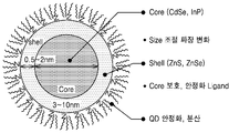
도 22는 본 발명의 기술적 사상의 일 실시예에 의한 발광 소자 패키지에 이용될 수 있는 파장 변환 물질로써 양자점(quantum dot, QD)의 단면 구조를 나타내는 개략도이다.
도 23은 본 발명의 기술적 사상의 일 실시예에 의한 발광 소자 패키지를 포함하는 백라이트 유닛의 개략적인 사시도이다.
도 24는 본 발명의 기술적 사상의 일 실시예에 의한 발광 소자 패키지를 포함하는 직하형 백라이트 유닛의 일 실시예를 나타내는 도면이다.
도 25는 본 발명의 기술적 사상의 일 실시예에 의한 발광 소자 패키지를 포함하는 백라이트 유닛의 일 실시예를 나타내는 도면이다.
도 26은 본 발명의 기술적 사상의 일 실시예에 의한 발광 소자 패키지를 포함하는 직하형 백라이트 유닛을 설명하기 위한 도면이다.
도 27은 도 26의 광원 모듈을 확대하여 도시한 도면이다.
도 28은 본 발명의 기술적 사상의 일 실시예에 의한 발광 소자 패키지를 포함하는 직하형 백라이트 유닛을 설명하기 위한 도면이다.
도 29 내지 도 31은 본 발명의 기술적 사상의 일 실시예에 의한 발광 소자 패키지를 포함하는 백라이트 유닛을 설명하기 위한 도면이다.
도 32는 본 발명의 기술적 사상의 일 실시예에 의한 발광 소자 패키지를 포함하는 디스플레이 장치의 개략적인 분해 사시도이다.
도 33은 본 발명의 기술적 사상의 일 실시예에 의한 발광 소자 패키지를 포함하는 평판 조명 장치를 간략하게 나타내는 사시도이다.
도 34는 본 발명의 기술적 사상의 일 실시예에 의한 발광 소자 패키지를 포함하는 조명 장치를 간략하게 나타내는 분해 사시도이다.
도 35는 본 발명의 기술적 사상의 일 실시예에 의한 발광 소자 패키지를 포함하는 바(bar) 타입의 조명 장치를 개략적으로 나타내는 분해 사시도이다.
도 36은 본 발명의 기술적 사상의 일 실시예에 의한 발광 소자 패키지를 구비하는 조명 장치를 개략적으로 나타내는 분해 사시도이다.
도 37은 본 발명의 기술적 사상의 일 실시예에 의한 발광 소자 패키지를 구비하는 실내용 조명 제어 네트워크 시스템을 설명하기 위한 개략도이다.
도 38은 본 발명의 기술적 사상의 일 실시예에 의한 발광 소자 패키지를 구비하는 네트워크 시스템을 설명하기 위한 개략도이다.
도 39는 본 발명의 기술적 사상의 일 실시예에 의한 발광 소자 패키지를 구비하는 조명 기구의 스마트 엔진과 모바일 기기의 통신 동작을 설명하기 위한 블록도이다.
도 40은 본 발명의 기술적 사상의 일 실시예에 의한 발광 소자 패키지를 구비하는 스마트 조명 시스템을 모식적으로 나타낸 개념도이다.1 is a cross-sectional view of a main portion of a light emitting device package according to an embodiment of the present invention.
FIG. 2 is a cross-sectional view showing a principal part of a light emitting device package according to an embodiment of the present invention.
3 is a cross-sectional view of a main part of a light emitting device package according to an embodiment of the technical idea of the present invention.
4 is a partial cross-sectional view of a light emitting device package according to an embodiment of the present invention.
5 is a cross-sectional view of a main portion of a light emitting device package according to an embodiment of the technical idea of the present invention.
6 is a cross-sectional view of a main portion of a light emitting device package according to an embodiment of the technical idea of the present invention.
7 to 10 are cross-sectional views illustrating major steps of the method of manufacturing the light emitting device package of FIG.
11 is a cross-sectional view illustrating a method of manufacturing the light emitting device package of FIG.
12 is a cross-sectional view illustrating a method of manufacturing the light emitting device package of FIG.
13 is a cross-sectional view illustrating a method of manufacturing the light emitting device package of FIG.
FIGS. 14 and 15 are cross-sectional views illustrating major steps of the method of manufacturing the light emitting device package of FIG.
16 is a cross-sectional view illustrating a method of manufacturing the light emitting device package of FIG.
17 is a cross-sectional view illustrating a method of manufacturing the light emitting device package of FIG.
18 and 19 are schematic cross-sectional views of a white light source module including a light emitting device package according to an embodiment of the present invention.
20 is a schematic cross-sectional view of a white light source module that can be used in a lighting apparatus as a light emitting device package according to an embodiment of the present invention.
21 is a CIE chromaticity diagram showing a complete photocell spectrum which can be used in a light emitting device package manufactured using the technical idea of the present invention.
22 is a schematic view showing a cross-sectional structure of a quantum dot (QD) as a wavelength converting material that can be used in a light emitting device package according to an embodiment of the present invention.
23 is a schematic perspective view of a backlight unit including a light emitting device package according to an embodiment of the present invention.
24 is a view showing an embodiment of a direct-type backlight unit including a light emitting device package according to an embodiment of the technical idea of the present invention.
25 is a view showing an embodiment of a backlight unit including a light emitting device package according to an embodiment of the present invention.
26 is a view for explaining a direct-type backlight unit including a light emitting device package according to an embodiment of the technical idea of the present invention.
FIG. 27 is an enlarged view of the light source module of FIG. 26; FIG.
28 is a view for explaining a direct-type backlight unit including a light emitting device package according to one embodiment of the technical idea of the present invention.
29 to 31 are views illustrating a backlight unit including a light emitting device package according to an embodiment of the present invention.
32 is a schematic exploded perspective view of a display device including a light emitting device package according to an embodiment of the present invention.
33 is a cross-sectional view of a light emitting device package according to an embodiment of the present invention; 1 is a perspective view schematically showing a flat panel illumination device.
34 is an exploded perspective view schematically illustrating a lighting device including a light emitting device package according to an embodiment of the present invention.
35 is an exploded perspective view schematically showing a bar-type lighting apparatus including a light emitting device package according to an embodiment of the technical idea of the present invention.
FIG. 36 is an exploded perspective view schematically showing a lighting apparatus having a light emitting device package according to an embodiment of the present invention.
37 is a schematic view for explaining an indoor lighting control network system having a light emitting device package according to an embodiment of the present invention.
38 is a schematic view for explaining a network system including a light emitting device package according to an embodiment of the present invention.
FIG. 39 is a block diagram for explaining a communication operation between a smart engine and a mobile device of a lighting device having a light emitting device package according to an embodiment of the present invention.
FIG. 40 is a conceptual diagram schematically showing a smart lighting system having a light emitting device package according to an embodiment of the present invention.
이하, 첨부된 도면을 참조하여 본 발명의 구체적인 실시예를 상세히 설명하기로 한다. 본 발명의 실시예들은 당해 기술 분야에서 통상의 지식을 가진 자에게 본 발명을 더욱 완전하게 설명하기 위하여 제공되는 것이며, 하기 실시예는 여러 가지 다른 형태로 변형될 수 있으며, 본 발명의 범위가 하기 실시예에 한정되는 것은 아니다. 오히려 이들 실시예들은 본 개시를 더욱 충실하고 완전하게 하고, 당업자에게 본 발명의 사상을 완전하게 전달하기 위하여 제공되는 것이다. 또한, 도면에서 각 층의 두께나 크기는 설명의 편의 및 명확성을 위하여 과장된 것이다.Hereinafter, embodiments of the present invention will be described in detail with reference to the accompanying drawings. The embodiments of the present invention are described in order to more fully explain the present invention to those skilled in the art, and the following embodiments may be modified into various other forms, The present invention is not limited to the embodiment. Rather, these embodiments are provided so that this disclosure will be more thorough and complete, and will fully convey the concept of the invention to those skilled in the art. In the drawings, the thickness and size of each layer are exaggerated for convenience and clarity of explanation.
명세서 전체에 걸쳐서, 막, 영역 또는 웨이퍼(기판) 등과 같은 하나의 구성요소가 다른 구성요소 "상에", "연결되어", 또는 "커플링되어" 위치한다고 언급할 때는, 상술한 하나의 구성요소가 직접적으로 다른 구성요소 "상에", "연결되어", 또는 "커플링되어" 접촉하거나, 그 사이에 개재되는 또 다른 구성요소들이 존재할 수 있다고 해석될 수 있다. 반면에, 하나의 구성요소가 다른 구성요소 "직접적으로 상에", "직접 연결되어", 또는 "직접 커플링되어" 위치한다고 언급할 때는, 그 사이에 개재되는 다른 구성요소들이 존재하지 않는다고 해석된다. 동일한 부호는 동일한 요소를 지칭한다. 본 명세서에서 사용된 바와 같이, 용어 "및/또는"은 해당 열거된 항목 중 어느 하나 및 하나 이상의 모든 조합을 포함한다.It is to be understood that throughout the specification, when an element such as a film, region or wafer (substrate) is referred to as being "on", "connected", or "coupled to" another element, It will be appreciated that elements may be directly "on", "connected", or "coupled" to another element, or there may be other elements intervening therebetween. On the other hand, when one element is referred to as being "directly on", "directly connected", or "directly coupled" to another element, it is interpreted that there are no other components intervening therebetween do. Like numbers refer to like elements. As used herein, the term "and / or" includes any and all combinations of one or more of the listed items.
본 명세서에서 제1, 제2등의 용어가 다양한 부재, 부품, 영역, 층들 및/또는 부분들을 설명하기 위하여 사용되지만, 이들 부재, 부품, 영역, 층들 및/또는 부분들은 이들 용어에 의해 한정되어서는 안됨은 자명하다. 이들 용어는 하나의 부재, 부품, 영역, 층 또는 부분을 다른 영역, 층 또는 부분과 구별하기 위하여만 사용된다. 따라서, 이하 상술할 제1부재, 부품, 영역, 층 또는 부분은 본 발명의 가르침으로부터 벗어나지 않고서도 제2부재, 부품, 영역, 층 또는 부분을 지칭할 수 있다.Although the terms first, second, etc. are used herein to describe various elements, components, regions, layers and / or portions, these members, components, regions, layers and / It is obvious that no. These terms are only used to distinguish one member, component, region, layer or section from another region, layer or section. Thus, a first member, component, region, layer or section described below may refer to a second member, component, region, layer or section without departing from the teachings of the present invention.
또한, "상의" 또는 "위의" 및 "하의" 또는 "아래의"와 같은 상대적인 용어들은 도면들에서 도해되는 것처럼 다른 요소들에 대한 어떤 요소들의 관계를 기술하기 위해 여기에서 사용될 수 있다. 상대적 용어들은 도면들에서 묘사되는 방향에 추가하여 소자의 다른 방향들을 포함하는 것을 의도한다고 이해될 수 있다. 예를 들어, 도면들에서 소자가 뒤집어 진다면(turned over), 다른 요소들의 상부의 면 상에 존재하는 것으로 묘사되는 요소들은 상술한 다른 요소들의 하부의 면 상에 방향을 가지게 된다. 그러므로, 예로써 든 "상의"라는 용어는, 도면의 특정한 방향에 의존하여 "하의" 및 "상의" 방향 모두를 포함할 수 있다. 구성 요소가 다른 방향으로 향한다면(다른 방향에 대하여 90도 회전), 본 명세서에 사용되는 상대적인 설명들은 이에 따라 해석될 수 있다.Also, relative terms such as "top" or "above" and "under" or "below" can be used herein to describe the relationship of certain elements to other elements as illustrated in the Figures. Relative terms are intended to include different orientations of the device in addition to those depicted in the Figures. For example, in the drawings, elements are turned over so that the elements depicted as being on the upper surface of the other elements are oriented on the lower surface of the other elements described above. Thus, the example "top" may include both "under" and "top" directions depending on the particular orientation of the figure. Relative descriptions used herein may be interpreted accordingly if the components are oriented in different directions (rotated 90 degrees with respect to the other direction).
본 명세서에서 사용된 용어는 특정 실시예를 설명하기 위하여 사용되며, 본 발명을 제한하기 위한 것이 아니다. 본 명세서에서 사용된 바와 같이, 단수 형태는 문맥상 다른 경우를 분명히 지적하는 것이 아니라면, 복수의 형태를 포함할 수 있다. 또한, 본 명세서에서 사용되는 경우 "포함한다(comprise)" 및/또는 "포함하는(comprising)"은 언급한 형상들, 숫자, 단계, 동작, 부재, 요소 및/또는 이들 그룹의 존재를 특정하는 것이며, 하나 이상의 다른 형상, 숫자, 동작, 부재, 요소 및/또는 그룹들의 존재 또는 부가를 배제하는 것이 아니다.The terminology used herein is for the purpose of describing particular embodiments only and is not intended to be limiting of the invention. As used herein, the singular forms "a," "an," and "the" include singular forms unless the context clearly dictates otherwise. Also, " comprise "and / or" comprising "when used herein should be interpreted as specifying the presence of stated shapes, numbers, steps, operations, elements, elements, and / And does not preclude the presence or addition of one or more other features, integers, operations, elements, elements, and / or groups.
이하, 본 발명의 실시예들은 본 발명의 이상적인 실시예들을 개략적으로 도시하는 도면들을 참조하여 설명한다. 도면들에 있어서, 예를 들면, 제조 기술 및/또는 공차(tolerance)에 따라, 도시된 형상의 변형들이 예상될 수 있다. 따라서, 본 발명 사상의 실시예는 본 명세서에 도시된 영역의 특정 형상에 제한된 것으로 해석되어서는 아니 되며, 예를 들면 제조상 초래되는 형상의 변화를 포함하여야 한다. 이하 실시예들은 하나 또는 복수개를 조합하여 구성할 수도 있다.Hereinafter, embodiments of the present invention will be described with reference to the drawings schematically showing ideal embodiments of the present invention. In the figures, for example, variations in the shape shown may be expected, depending on manufacturing techniques and / or tolerances. Accordingly, the embodiments of the present invention should not be construed as limited to the particular shapes of the regions illustrated herein, but should include, for example, changes in shape resulting from manufacturing. The following embodiments may be constructed by combining one or a plurality of embodiments.
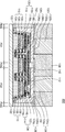
도 1은 본 발명의 기술적 사상의 일 실시예에 의한 발광 소자 패키지의 요부 단면도이다.1 is a cross-sectional view of a main portion of a light emitting device package according to an embodiment of the present invention.
구체적으로, 본 발명의 일 실시예에 의한 발광 소자 패키지(100)는 칩 스케일 패키지(Chip Scale Package, CSP)나 웨이퍼 레벨 패키지(Wafer Level Package, WLP)일 수 있다. 앞서 설명한 바와 같이 본 명세서에서, '상', '상부', '상면', '하', '하부', '하면', '측면' 등의 용어는 도면을 기준으로 한 것이며, 실제로는 소자나 패키지가 배치되는 방향에 따라 달라질 수 있다. 본 명세서에서의 도면들은 필요한 구성 요소만을 도시한 것이다. 본 명세서에서의 도면들은 발광 소자 패키지(100)의 일부만을 도시한 것이다. Specifically, the light emitting
발광 소자 패키지(100)는 제1 도전형 반도체층(104), 활성층(106) 및 제2 도전형 반도체층(108)을 구비하는 발광 구조물(110)을 포함할 수 있다. 발광 구조물(110)은 다양한 구조를 가질 수 있지만 본 실시예에서는 메사형 발광 구조물을 예로 도시한다. 발광 소자 패키지(100)는 도면에서 발광 구조물(110)을 세 개 표시하지만 이는 설명의 편의를 위한 것이고, 더 많은 수의 발광 구조물(110)을 포함할 수 있다. The light emitting
발광 구조물(110)은 기판(102) 상에 형성될 수 있다. 기판(102)은 반도체 웨이퍼 일 수 있다. 기판(102)은 실리콘계 기판일 수 있다. 실리콘계 기판은 실리콘(Si) 기판 또는 실리콘 카바이드 기판(SiC)일 수 있다. 기판(102)으로 실리콘계 기판을 이용할 경우, 대구경화에 보다 적합하고 상대적으로 가격이 낮아 패키지 생산성이 향상될 수 있다.The
기판(102)은 사파이어, MgAl2O4, MgO, LiAlO2, LiGaO2, GaN 등과 같이 절연성, 도전성, 또는 반도체 물질을 이용할 수 있다. 사파이어는, 전기 절연성을 가지며 육각-롬보형(Hexa-Rhombo R3c) 대칭성을 갖는 결정체로서 c축 및 a측 방향의 격자 상수가 각각 13.001Å과 4.758Å이며, C(0001)면, A(1120)면, R(1102)면 등을 가질 수 있다. 이 경우, C면은 비교적 질화물 박막의 성장이 용이하며, 고온에서 안정하기 때문에 질화물 성장용 기판으로 사용될 수 있다.The
발광 구조물(110)을 구성하는 제1 도전형 반도체층(104)은 n형 반도체층일 수 있다. 발광 구조물(110)을 구성하는 제2 도전형 반도체층(108)은 p형 반도체층일 수 있다. 제1 도전형 반도체층(104) 및 제2 도전형 반도체층(108)은 질화물 반도체, 예컨대, GaN/InGaN 물질로 이루어질 수 있다. The first
제1 도전형 반도체층(104) 및 제2 도전형 반도체층(108)은 질화물 반도체, 예컨대, AlxInyGa1-x-yN (0≤x≤1, 0≤y≤1, 0≤x+y≤1)의 조성을 갖는 물질로 이루어질 수 있다. 제1 도전형 반도체층(104) 및 제2 도전형 반도체층(108)은 단일층으로 이루어질 수도 있지만, 도핑 농도, 조성 등의 특성이 서로 다른 복수의 층을 구비할 수도 있다. 제1 도전형 반도체층(104) 및 제2 도전형 반도체층(108)은 질화물 반도체 외에도 AlInGaP나 AlInGaAs 계열의 반도체를 이용할 수도 있다. The first
제1 도전형 반도체층(104)과 제2 도전형 반도체층(108)의 사이에 배치된 활성층(106)은 전자와 정공의 재결합에 의해 소정의 에너지를 갖는 광을 방출할 수 있다. 활성층(106)은 양자 우물층과 양자 장벽층이 서로 교대로 적층된 다중 양자우물(MQW)구조, 예컨대, 질화물 반도체일 경우, GaN/InGaN 구조가 사용될 수 있다. 활성층(106)은 질화물 반도체를 이용한 단일 양자우물(SQW) 구조가 사용될 수도 있다.The
발광 구조물(110)의 양측부 및 상부에는 다른 구성 요소들과 전기적 절연을 이루는 분리 절연층(112)이 형성되어 있다. 분리 절연층(112)은 실리콘 산화층으로 형성될 수 있다. 분리 절연층(112)은 메사형 발광 구조물(110)을 절연할 수 있다. 분리 절연층(112) 내에는 상기 제1 도전형 반도체층(104) 및 제2 도전형 반도체층(108)과 각각 전기적으로 연결된 제1 연결 전극부(120) 및 제2 연결 전극부(124)가 형성되어 있다. On both sides and top of the
제1 연결 전극부(120)는 분리 절연층(112)을 관통하는 기둥 전극층(118a)과 기둥 전극층(118a)과 연결되는 제1 평판 전극층(118b)을 포함하는 전극층(118)을 구비할 수 있다. 제1 연결 전극부(120)는 기둥 전극층(118a) 하부의 제1 도전형 반도체층(104) 상에 형성된 제1 콘택층(116)을 포함할 수 있다. 제1 콘택층(116)은 오믹 금속층일 수 있다. 제1 콘택층(116)은 도전성 물질층, 예컨대 Ag, Al, Ni, Cr, Cu, Au, Pd, Pt, Sn, W, Rh, Ir, Ru, Mg, Zn, Ti 또는 이들을 포함하는 합금 물질 중 하나 이상으로 이루어질 수 있다.The first
제2 연결 전극부(124)는 제2 도전형 반도체층(108) 상부의 분리 절연층(112) 내에 형성된 제2 평판 전극층(122)을 포함할 수 있다. 제2 연결 전극부(124)는 제2 평판 전극층(122) 하부의 제2 도전형 반도체층(108) 상에 형성된 제2 콘택층(114)을 포함할 수 있다. 제2 콘택층(114)은 접착 성질과 반사 성질을 갖는 두개의 금속층(114a, 114b)을 포함할 수 있다. 제2 콘택층(114)은 제1 콘택층(116)과 동일한 물질로 구성될 수 있다. The second
제1 연결 전극부(120) 및 제2 연결 전극부(124)의 상부 및 분리 절연층(112) 상에는 제1 연결 전극부(120) 및 제2 연결 전극부(124)와 각각 전기적으로 연결된 제1 전극 패드(126) 및 제2 전극 패드(128)가 형성되어 있다. 제1 전극 패드(126) 및 제2 전극 패드(128)는 발광 구조물(110)의 상부 및 양측부에 형성되어 있는 분리 절연층(112) 상에 형성되어 있다. The first
제1 전극 패드(126)는 제1 평판 전극층(118b)과 전기적으로 연결된 제1 패드 씨드층(126a) 및 제1 패드 씨드층(126a) 상에 형성된 제1 패드층(126b)을 포함할 수 있다. 제2 전극 패드(128)는 제2 평판 전극층(122)과 전기적으로 연결된 제2 패드 씨드층(128a) 및 제2 패드 씨드층(128a) 상에 형성된 제2 패드층(128b)을 포함할 수 있다. 제1 패드 씨드층(126a), 제2 패드 씨드층(128a), 제1 패드층(126b) 및 제2 패드층(128b)은 금속층, 예컨대 구리층으로 구성할 수 있다. The
제1 전극 패드(126) 및 제2 전극 패드(128) 사이에는 제1 몰딩 수지층(130)이 형성되어 있다. 제1 몰딩 수지층(130)은 발광 구조물(110) 상부의 제1 전극 패드(126) 및 제2 전극 패드(128) 사이, 및 발광 구조물(110) 일측부의 제1 전극 패드(126) 및 제2 전극 패드(128) 사이에 형성될 수 있다. 제1 몰딩 수지층(130)은 제1 전극 패드(126) 및 제2 전극 패드(128) 사이를 밀봉하는 밀봉층(encapsulation layer)일 수 있다. A first
제1 몰딩 수지층(130)은 후에 설명되는 제2 몰딩 수지층(138)보다 반사율이 높은 물질층으로 구성할 수 있다. 제1 몰딩 수지층(130)은 반사율이 높은 물질, 예컨대 텅스텐이나 실리콘 물질을 포함하여 후에 설명되는 제2 몰딩 수지층보다 반사율이 높을 수 있다. 제1 몰딩 수지층(130)으로 인하여 발광 소자 패키지(100)의 광 추출 효율을 향상시킬 수 있다.The first
제1 전극 패드(126) 및 제2 전극 패드(128)와, 제1 몰딩 수지층(130)이 형성될 경우, 발광 소자 패키지(100)는 평면이나 단면으로 패드 영역(PD1, PD2) 및 패드 분리 영역(PDIS)으로 구분할 수 있다. 패드 영역(PD1, PD2)은 제1 패드 영역(PD1) 및 제2 패드 영역(PD2)으로 구분할 수 있다. 제1 패드 영역(PD1)은 제1 도전형 반도체층(104), 활성층(106) 및 제2 도전형 반도체층(108)을 구비하는 발광 구조물(110)을 포함하고, 상기 제1 도전형 반도체층(104)과 전기적으로 연결되는 제1 전극 패드(126)를 포함할 수 있다. When the
제2 패드 영역(PD2)은 발광 구조물(110)을 포함하고, 제2 도전형 반도체층(108)과 전기적으로 연결되는 제2 전극 패드(128)를 포함할 수 있다. 패드 분리 영역(PDIS)은 제1 패드 영역(PD1)과 제2 패드 영역(PD2)을 전기적으로 분리하도록 제1 몰딩 수지층(130)으로 구성될 수 있다. The second pad region PD2 may include a
제1 전극 패드(126) 및 제2 전극 패드(128) 상에 제1 전극 패드(126) 및 제2 전극 패드(128)와 각각 전기적으로 연결된 제1 필라 전극(132) 및 제2 필라 전극(134)이 형성되어 있다. 제1 패드 영역(PD1)의 제1 전극 패드(126) 및 제2 패드 영역(PD2)의 제2 전극 패드(128) 상에 각각 제1 필라 전극(132) 및 제2 필라 전극(134)이 형성되어 있다. The
제1 필라 전극(132) 및 제2 필라 전극(134)은 솔더볼을 이용하거나 플립칩 형태로 외부 배선 기판(미도시)에 전기적으로 연결될 수 있다. 제1 필라 전극(132)은 제1 전극 패드(126)와 전기적으로 연결된 제1 필라 씨드층(132a) 및 제1 필라 씨드층(132a) 상에 형성된 제1 필라층(132b)을 포함할 수 있다. The
제2 필라 전극(134)은 제2 전극 패드(128)와 전기적으로 연결된 제2 필라 씨드층(134a) 및 제2 필라 씨드층(134a) 상에 형성된 제2 필라층(134b)을 포함할 수 있다. 제1 필라 씨드층(132a), 제2 필라 씨드층(134a), 제1 필라층(132b) 및 제2 필라층(134b)은 금속층, 예컨대 구리층으로 구성할 수 있다. The
제1 몰딩 수지층(130), 제1 전극 패드(126) 및 제2 전극 패드(128) 상에서 제1 필라 전극(132) 및 제2 필라 전극(134) 사이에 제2 몰딩 수지층(138)이 형성되어 있다. 제2 몰딩 수지층(138)은 제1 패드 영역(PD1)의 제1 필라 전극(132) 및 제2 패드 영역(PD2)의 제2 필라 전극(134) 사이와 패드 분리 영역(PDIS)에 위치할 수 있다. 제2 몰딩 수지층(138)은 제1 필라 전극(132) 및 제2 필라 전극(134) 사이를 밀봉하는 밀봉층일 수 있다. A second
제2 몰딩 수지층(138)은 제1 몰딩 수지층(130)에 비해 신뢰성이 높은 물질층으로 구성할 수 있다. 제2 몰딩 수지층(138)은 제1 몰딩 수지층(130)에 비하여 습윤성, 내성 및 강성 등의 신뢰성이 좋은 물질로 구성할 수 있다. The second
이상과 같이 발광 소자 패키지(100)는 제1 전극 패드(126) 및 제2 전극 패드(128) 사이에 반사율이 높은 제1 몰딩 수지층(130)이 형성되어 있다. 발광 소자 패키지(100)는 제1 필라 전극(132) 및 제2 필라 전극(134) 사이에 신뢰성이 높은 제2 몰딩 수지층(138)이 형성되어 있다. 이에 따라, 발광 소자 패키지(100)는 광 추출 효율을 높이면서도 신뢰성을 향상시킬 수 있다.As described above, the first
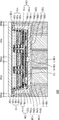
도 2는 본 발명의 기술적 사상의 일 실시예에 의한 발광 소자 패키지의 요부 단면도이다.FIG. 2 is a cross-sectional view showing a principal part of a light emitting device package according to an embodiment of the present invention.
구체적으로, 발광 소자 패키지(200)는 도 1과 비교할 때 제1 몰딩 수지층(130) 상에 제1 반사층(142)이 더 형성된 것을 제외하고는 동일할 수 있다. 이에 따라, 도 2의 설명에서 도 1과 동일한 것은 생략하거나 간단히 설명한다.Specifically, the light emitting
발광 소자 패키지(200)는 제1 전극 패드(126) 및 제2 전극 패드(128) 사이에 형성된 제1 몰딩 수지층(130) 상에 제1 반사층(142)이 더 형성되어 있다. 패드 분리 영역(PDIS)의 제1 몰딩 수지층(130) 상에는 제1 반사층(142)이 더 형성되어 있다. 제1 반사층(142)은 금속층, 예컨대 구리층으로 구성할 수 있다. 제1 반사층(142)은 제1 필라 씨드층(132a) 및 제2 필라 씨드층(134a)과 동일 물질로 구성할 수 있다.The light emitting
이상과 같은 발광 소자 패키지(200)는 제1 몰딩 수지층(130) 상에 제1 반사층(142)을 포함하여 구성함으로써 발광 구조물(110)에서 발광되는 광을 보다 더 잘 외부로 배출할 수 있다. 결과적으로, 발광 소자 패키지(200)는 광 추출 효율을 더욱더 향상시킬 수 있다. The light emitting
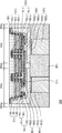
도 3은 본 발명의 기술적 사상의 일 실시예에 의한 발광 소자 패키지의 요부 단면도이다.3 is a cross-sectional view of a main part of a light emitting device package according to an embodiment of the technical idea of the present invention.
구체적으로, 발광 소자 패키지(300)는 도 1과 비교할 때 제1 몰딩 수지층(130-1) 및 제2 몰딩 수지층(138-1)의 형성 위치가 다른 것을 제외하고는 동일할 수 있다. 이에 따라, 도 3의 설명에서 도 1과 동일한 것은 생략하거나 간단히 설명한다.Specifically, the light emitting
발광 소자 패키지(300)는 제1 몰딩 수지층(130-1) 및 제2 몰딩 수지층(138-1)을 포함할 수 있다. 제1 몰딩 수지층(130-1)은 제1 전극 패드(126) 및 제2 전극 패드(128)의 표면 및 양측벽에 형성되어 있다. 제1 몰딩 수지층(130-1)은 제1 필라 전극(132) 및 제2 필라 전극(134)의 양측벽에 형성되어 제1 필라 전극(132) 및 제2 필라 전극(134) 사이에 위치할 수 있다. The light emitting
제1 몰딩 수지층(130-1)은 제1 전극 패드(126) 및 제2 전극 패드(128) 사이에 위치하는 도포형 수지층일 수 있다. 제1 몰딩 수지층(130-1)은 제1 필라 전극(132) 및 제2 필라 전극(134) 사이에 위치하는 도포형 수지층일 수 있다. 제1 몰딩 수지층(130-1)은 후에 형성되는 제2 몰딩 수지층(138-1)보다 반사율이 높은 물질로 구성할 수 있다. The first molding resin layer 130-1 may be a coating type resin layer positioned between the
제2 몰딩 수지층(138-1)은 일측벽에 제1 몰딩 수지층(130-1)이 형성된 제1 필라 전극(132) 및 제2 필라 전극(134) 사이에 형성될 수 있다. 제2 몰딩 수지층(138-1)은 제1 전극 패드(126) 및 제2 전극 패드(128)의 일측벽에 형성된 제1 몰딩 수지층(130-1) 상에 형성되어 있다. 제2 몰딩 수지층(138-1)은 패드 분리 영역(PDIS)에서 제1 몰딩 수지층(130-1)의 일측에 형성되어 있다. 제2 몰딩 수지층(138-1)은 제1 전극 패드(126) 및 제2 전극 패드(128) 사이에 위치할 수 있다. 제2 몰딩 수지층(138-1)은 제1 몰딩 수지층(130-1)에 비하여 신뢰성이 높은 물질로 구성할 수 있다.The second molding resin layer 138-1 may be formed between the
이상과 같이 발광 소자 패키지(300)는 제1 전극 패드(126) 및 제2 전극 패드(128)의 표면 및 양측벽과, 제1 필라 전극(132) 및 제2 필라 전극(134)의 양측벽에 반사율이 높은 제1 몰딩 수지층(130-1)이 형성되어 있다. 발광 소자 패키지(300)는 제1 필라 전극(132) 및 제2 필라 전극(134) 사이와 제1 전극 패드(126) 및 제2 전극 패드(128)의 일측벽에 형성된 제1 몰딩 수지층(130-1) 상에 신뢰성이 높은 제2 몰딩 수지층(138-1)이 형성되어 있다. 이에 따라, 발광 소자 패키지(300)는 광 추출 효율을 높이면서도 신뢰성을 향상시킬 수 있다.As described above, the light emitting
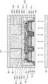
도 4는 본 발명의 기술적 사상의 일 실시예에 의한 발광 소자 패키지의 요부 단면도이다.4 is a partial cross-sectional view of a light emitting device package according to an embodiment of the present invention.
구체적으로, 발광 소자 패키지(400)는 도 1 및 도 3과 비교할 때 제1 몰딩 수지층(130-1) 및 제2 몰딩 수지층(138-1) 사이에 제2 반사층(148)이 더 형성된 것을 제외하고는 동일할 수 있다. 이에 따라, 도 4의 설명에서 도 1 및 도 3과 동일한 것은 생략하거나 간단히 설명한다.1 and 3, the light emitting
제1 전극 패드(126) 및 제2 전극 패드(128)의 표면 및 양측벽과, 제1 필라 전극(132) 및 제2 필라 전극(134)의 양측벽에 형성된 제1 몰딩 수지층(130-1) 상에 제2 반사층(148)이 형성되어 있다. 제2 반사층(148)은 금속층, 예컨대 은(Ag) 또는 구리(Cu)로 형성할 수 있다. 제2 반사층(148)은 분산 브래그 반사층(distributed Bragg reflector)이 이용될 수 있다. 분산 브래그 반사층은 제1 굴절률을 갖는 제1 절연막과 제2 굴절률을 갖는 제2 절연막이 교대로 적층된 다층 반사층일 수 있다. The first and
제2 반사층(148) 상에는 제2 몰딩 수지층(138-1)이 형성되어 있다. 이에 따라, 제2 반사층(148)은 제1 몰딩 수지층(130-1) 및 제2 몰딩 수지층(138-1) 사이에 위치할 수 있다. 제2 반사층(148)은 제1 패드 영역(PD1), 제2 패드 영역(PD2) 및 패드 분리 영역(PDIS)의 제1 몰딩 수지층(130-1)과 제2 몰딩 수지층(138-1) 사이에는 위치할 수 있다. A second molding resin layer 138-1 is formed on the second
이상과 같은 발광 소자 패키지(400)는 제1 몰딩 수지층(130-1)의 전면에 제2 반사층(148)을 위치시킴으로써 발광 구조물(110)에서 발광되는 광을 보다 더 잘 외부로 배출할 수 있다. 결과적으로, 발광 소자 패키지(400)는 광 추출 효율을 더욱더 향상시킬 수 있다.In the light emitting
도 5 및 도 6은 본 발명의 기술적 사상의 일 실시예에 의한 발광 소자 패키지의 요부 단면도이다.5 and 6 are cross-sectional views of a main portion of a light emitting device package according to an embodiment of the present invention.
구체적으로, 발광 소자 패키지(500, 600)는 도 1 및 도 3과 비교할 때 기판(102)을 제거한 것을 제외하고는 동일할 수 있다. 이에 따라, 도 5 및 도 6의 설명에서 도 1, 도 2 및 도 3과 동일한 것은 생략하거나 간단히 설명한다.Specifically, the light emitting device packages 500 and 600 may be the same, except that the
발광 소자 패키지(500, 600)는 도 1 및 도 3의 발광 소자 패키지(100, 300)에서 기판(102)를 제거한 것을 나타낸 것이다. 기판(102)을 제거할 경우, 발광 구조물(110)에서 발광되는 광이 기판(102)에서 흡수되지 않을 수 있다. The light emitting device packages 500 and 600 show the
이에 따라, 발광 소자 패키지(500, 600)는 제2 몰딩 수지층(138, 138-1)을 포함하여 신뢰성을 향상시킬 수 있고, 아울러서 제1 몰딩 수지층(130, 130-1)을 포함함과 아울러 기판(102)으로 광이 흡수되지 않아 광 추출 효율을 더욱더 향상시킬 수 있다. Accordingly, the light emitting device packages 500 and 600 include the second molding resin layers 138 and 138-1 to improve reliability, and further include the first molding resin layers 130 and 130-1. The light is not absorbed by the
도 7 내지 도 10은 도 1의 발광 소자 패키지의 제조 방법을 개략적으로 나타내는 주요 단계별 단면도들이다. 도 7 내지 도 10의 설명에서 도 1에서 설명한 것과 동일한 것은 생략하거나 간단히 설명한다.7 to 10 are cross-sectional views illustrating major steps of the method of manufacturing the light emitting device package of FIG. In the description of Figs. 7 to 10, the same elements as those described in Fig. 1 are omitted or briefly described.
도 7을 참조하면, 기판(102) 상에 제1 도전형 반도체층(104), 활성층(106) 및 제2 도전형 반도체층(108)을 구비하는 발광 구조물(110)을 형성한다. 발광 구조물(110)의 양측부 및 상부에는 다른 구성 요소들과 전기적 절연을 이루는 분리 절연층(112)을 형성한다. Referring to FIG. 7, a
분리 절연층(112) 내에는 상기 제1 도전형 반도체층(104) 및 제2 도전형 반도체층(108)과 각각 전기적으로 연결되는 제1 연결 전극부(120) 및 제2 연결 전극부(124)를 형성한다. The first
제1 연결 전극부(120)는 분리 절연층(112)을 관통하는 기둥 전극층(118a)과 기둥 전극층(118a)과 연결되는 제1 평판 전극층(118b)을 포함하는 전극층(118)을 구비할 수 있다. 제1 연결 전극부(120)는 기둥 전극층(118a) 하부의 제1 도전형 반도체층(104) 상에 형성된 제1 콘택층(116)을 포함할 수 있다. The first
제2 연결 전극부(124)는 제2 도전형 반도체층(108) 상부의 분리 절연층(112)내에 형성된 제2 평판 전극층(122)을 포함할 수 있다. 제2 연결 전극부(124)는 제2 평판 전극층(122) 하부의 제2 도전형 반도체층(108) 상에 형성된 제2 콘택층(114)을 포함할 수 있다. The second
제1 연결 전극부(120) 및 제2 연결 전극부(124)의 상부 및 분리 절연층(112) 상에는 제1 연결 전극부(120) 및 제2 연결 전극부(124)와 각각 전기적으로 연결된 제1 전극 패드(126) 및 제2 전극 패드(128)를 형성한다. The first
제1 전극 패드(126) 및 제2 전극 패드(128)의 형성은 다음의 공정을 거칠 수는 있다. 즉, 제1 평판 전극층(118b) 및 제2 평판 전극층(122)과 전기적으로 연결되는 패드 씨드용 물질층 및 패드용 물질층을 형성한 후 사진식각공정을 이용하여 패터닝하여 형성할 수 있다. The
이에 따라, 제1 패드 씨드층(126a) 및 제2 패드 씨드층(128a) 상에 각각 제1 패드층(126b) 및 제2 패드층(128b)이 형성됨으로써 제1 전극 패드(126) 및 제2 전극 패드(128)가 마련될 수 있다. The
앞서의 사진 식각 공정을 통하여 제1 전극 패드(126) 및 제2 전극 패드(28) 사이에는 패드 분리홀들(152, 154)이 형성된다. 패드 분리홀(152)은 발광 구조물(110)의 상부에 형성되는 홀일 수 있고, 패드 분리홀(154)은 발광 구조물(110)의 양측부에 형성되는 홀일 수 있다.The pad isolation holes 152 and 154 are formed between the
도 8을 참조하면, 패드 분리홀(154) 내에 제1 몰딩 수지층(130)을 형성한다. 제1 몰딩 수지층(130)은 후에 형성되는 제2 몰딩 수지층(138)보다 반사율이 높은 물질층으로 구성할 수 있다. 제1 몰딩 수지층(130)은 제1 전극 패드(126) 및 제2 전극 패드(128) 사이를 밀봉하는 밀봉층(encapsulation layer)으로 형성한다. Referring to FIG. 8, a first
제1 몰딩 수지층(130)은 반사율이 높은 물질, 예컨대 텅스텐이나 실리콘 물질을 포함하여 후에 형성되는 제2 몰딩 수지층(도 1의 138)보다 반사율을 높게 한다. 제1 몰딩 수지층(130)으로 인하여 광 추출 효율을 향상시킬 수 있다.The first
도 9 및 도 10을 참조하면, 도 9에 도시한 바와 같이 제1 전극 패드(126) 및 제2 전극 패드(128)와 제1 몰딩 수지층(130) 상에 필라 씨드용 물질층(156)을 형성한다. 필라 씨드용 물질층(156)은 금속층, 예컨대 구리층으로 형성할 수 있다. 9 and 10, a pillar
도 10에 도시한 바와 같이, 필라 씨드용 물질층(156) 상에 필라 전극용 물질층(미도시)을 형성한 후, 필라 전극용 물질층 및 필라 씨드용 물질층(156)을 사진식각공정으로 패터닝하여 제1 필라 전극(132) 및 제2 필라 전극(134)을 형성한다. 필라 전극용 물질층은 금속층, 예컨대 구리층으로 형성할 수 있다. 10, a pillar electrode material layer (not shown) is formed on the pillar
제1 필라 전극(132)은 제1 필라 씨드층(132a) 및 제1 필라층(132b)으로 구성될 수 있다. 제2 필라 전극(134)은 제2 필라 씨드층(134a) 및 제2 필라층(134b)으로 구성할 수 있다. 결과적으로, 제1 필라 씨드층(132a), 제2 필라 씨드층(134a), 제1 필라층(132b) 및 제2 필라층(134b)은 금속층, 예컨대 구리층으로 형성할 수 있다. The
계속하여, 도 1에 도시한 바와 같이 제1 몰딩 수지층(130), 제1 전극 패드(126) 및 제2 전극 패드(128) 상에서 제1 필라 전극(132) 및 제2 필라 전극(134) 사이에 제2 몰딩 수지층(138)을 형성한다. 제2 몰딩 수지층(138)은 제1 필라 전극(132) 및 제2 필라 전극(134) 사이에 몰딩 물질층을 형성한 후 표면을 그라인딩하여 형성할 수 있다. 제2 몰딩 수지층(138)은 제1 필라 전극(132) 및 제2 필라 전극(134) 사이를 밀봉하는 밀봉층일 수 있다. 제2 몰딩 수지층(138)은 제1 몰딩 수지층(130)에 비하여 습윤성, 내성 및 강성 등의 신뢰성이 좋은 물질로 형성할 수 있다. 이와 같은 공정을 통하여 도 1의 발광 소자 패키지(100)가 완성될 수 있다.1, the
도 11은 도 2의 발광 소자 패키지의 제조 방법을 설명하기 위한 단면도이다.11 is a cross-sectional view illustrating a method of manufacturing the light emitting device package of FIG.
구체적으로, 도 11의 발광 소자 패키지의 제조 방법은 도 7 내지 도 9와 비교할 때 제1 반사층(142)을 형성하는 공정을 제외하고는 동일할 수 있다. 이에 따라, 도 11의 설명에서 도 7 내지 도 10의 설명과 동일한 것은 생략하거나 간단히 설명한다.Specifically, the manufacturing method of the light emitting device package of FIG. 11 may be the same as the manufacturing method of the light emitting device package, except for the step of forming the first
앞서 도 9, 도 10 및 도 11에 도시한 바와 같이 제1 전극 패드(126) 및 제2 전극 패드(128)와 제1 몰딩 수지층(130) 상에 필라 씨드용 물질층(156) 및 필라 전극용 물질층(미도시)을 형성한 후, 사진식각공정으로 패터닝할 때 제1 필라 전극(132) 및 제2 필라 전극(134)뿐만 아니라 제1 반사층(142)을 형성한다. 9, 10 and 11, a pillar
제1 반사층(142)은 제1 몰딩 수지층(130) 상에 형성될 수 있다. 제1 반사층(142)은 필라 씨드층(132a, 132b)과 동일한 물질로 형성할 수 있다. 제1 반사층(142)은 금속층, 예컨대 구리층으로 형성할 수 있다. The first
도 12는 도 5의 발광 소자 패키지의 제조 방법을 설명하기 위한 단면도이다.12 is a cross-sectional view illustrating a method of manufacturing the light emitting device package of FIG.
구체적으로, 도 12의 발광 소자 패키지의 제조 방법은 도 7 내지 도 9와 비교할 때 기판(102)을 제거하는 공정을 제외하고는 동일할 수 있다. 이에 따라, 도 12의 설명에서 도 7 내지 도 10의 설명과 동일한 것은 생략하거나 간단히 설명한다.Specifically, the manufacturing method of the light emitting device package of FIG. 12 may be the same, except for the step of removing the
도 7 및 도 8의 제조 공정을 수행한다. 도 7에 도시한 바와 같이 기판(102) 상에 제1 도전형 반도체층(104), 활성층(106) 및 제2 도전형 반도체층(108)을 구비하는 발광 구조물(110), 분리 절연층(112), 제1 연결 전극부(120), 제2 연결 전극부(124), 제1 전극 패드(126) 및 제2 전극 패드(128)를 형성한다. 이어서, 도 8에 도시한 바와 같이 제1 전극 패드(126) 및 제2 전극 패드(128) 사이를 밀봉하는 제1 몰딩 수지층(130)을 형성한다. The manufacturing process of Figs. 7 and 8 is carried out. A
계속하여, 도 12에 도시한 바와 같이 제1 전극 패드(126) 및 제2 전극 패드(128), 및 제1 몰딩 수지층(130)을 아래로 하여 지지 캐리어(158)에 부착시킨다. 이어서, 지지 캐리어(158)의 상부에 형성되어 있는 기판(102)을 제거한다. Subsequently, as shown in FIG. 12, the
다음에, 지지 캐리어(158)를 제거한 후, 도 9 및 도 10에 도시한 바와 같이 제1 전극 패드(126) 및 제2 전극 패드(128) 상에 제1 필라 전극(132) 및 제2 필라 전극(134)을 형성한다. 9 and 10, the
이어서, 도 5에 도시한 바와 같이 제1 몰딩 수지층(130), 제1 전극 패드(126) 및 제2 전극 패드(128) 상에서 제1 필라 전극(132) 및 제2 필라 전극(134) 사이에 제2 몰딩 수지층(138)을 형성함으로써 발광 소자 패키지(500)를 완성할 수 있다. 5, the
도 13은 도 5의 발광 소자 패키지의 제조 방법을 설명하기 위한 단면도이다. 13 is a cross-sectional view illustrating a method of manufacturing the light emitting device package of FIG.
구체적으로, 도 13의 발광 소자 패키지의 제조 방법은 도 7 내지 도 9와 비교할 때 기판(102)을 제거하는 공정을 제외하고는 동일할 수 있다. 이에 따라, 도 13의 설명에서 도 7 내지 도 10의 설명과 동일한 것은 생략하거나 간단히 설명한다.Specifically, the manufacturing method of the light emitting device package of FIG. 13 may be the same as the manufacturing method of the light emitting device package except for removing the
도 7 내지 도 10의 제조 공정을 수행한다. 아울러서, 도 5에 도시한 바와 같이 제1 몰딩 수지층(130), 제1 전극 패드(126) 및 제2 전극 패드(128) 상에서 제1 필라 전극(132) 및 제2 필라 전극(134) 사이에 제2 몰딩 수지층(138)을 형성한다. The manufacturing process of FIGS. 7 to 10 is carried out. 5, between the
계속하여, 도 13에 도시한 바와 같이 제1 필라 전극(132) 및 제2 필라 전극(134), 및 제2 몰딩 수지층(138)을 아래로 하여 지지 캐리어(158)에 부착시킨다. 이어서, 지지 캐리어(158)의 상부에 형성되어 있는 기판(102)을 제거한 후, 지지 캐리어(158)를 제거함으로써 발광 소자 패키지(500)를 완성할 수 있다.Subsequently, as shown in Fig. 13, the
도 14 및 도 15는 도 3의 발광 소자 패키지의 제조 방법을 개략적으로 나타내는 주요 단계별 단면도들이다. 도 14 및 도 15의 설명에서 도 3이나, 도 7 내지 도 10의 제조 방법에서 설명한 것과 동일한 것은 생략하거나 간단히 설명한다.FIGS. 14 and 15 are cross-sectional views illustrating major steps of the method of manufacturing the light emitting device package of FIG. In the description of Figs. 14 and 15, the same elements as those described in Figs. 3 and 7 to 10 are omitted or briefly explained.
앞서 도 7에서 설명한 바와 같이 기판(102) 상에 제1 도전형 반도체층(104), 활성층(106) 및 제2 도전형 반도체층(108)을 구비하는 발광 구조물(110), 분리 절연층(112), 제1 연결 전극부(120), 및 제2 연결 전극부(124)를 형성한다. The
그리고, 제1 연결 전극부(120) 및 제2 연결 전극부(124)와 각각 전기적으로 연결되는 제1 전극 패드(126) 및 제2 전극 패드(128)를 형성한다. 제1 전극 패드(126) 및 제2 전극 패드(28) 사이에는 패드 분리홀들(152, 154)이 형성된다. 패드 분리홀(152)은 발광 구조물(110)의 상부에 형성되는 홀일 수 있고, 패드 분리홀(154)은 발광 구조물(110)의 양측부에 형성되는 홀일 수 있다.The
도 14에 도시한 바와 같이, 제1 전극 패드(126) 및 제2 전극 패드(128) 상에 각각 제1 필라 전극(132) 및 제2 필라 전극(134)을 형성한다. 앞서 설명한 바와 같이 제1 필라 전극(132)은 제1 필라 씨드층(132a) 및 제1 필라층(132b)으로 구성될 수 있다. 제2 필라 전극(134)은 제2 필라 씨드층(134a) 및 제2 필라층(134b)으로 구성할 수 있다. The
도 15에 도시한 바와 같이, 제1 전극 패드(126), 제2 전극 패드(128), 제1 필라 전극(132) 및 제2 필라 전극(134)의 전면 및 패드 분리홀(152, 154)의 전면에 제1 몰딩 수지층(130-1)을 형성한다. 제1 몰딩 수지층(130-1)은 몰딩 수지를 스프레이 형태로 도포한 도포형 수지층일 수 있다. 제1 몰딩 수지층(130-1)은 후에 형성되는 제2 몰딩 수지층(138-1)보다 반사율이 높은 물질로 구성할 수 있다.15, the front surfaces of the
앞서 설명한 바와 같이 제1 몰딩 수지층(130-1)은 제1 전극 패드(126) 및 제2 전극 패드(128)의 표면 및 양측벽에 형성한다. 제1 몰딩 수지층(130-1)은 제1 필라 전극(132) 및 제2 필라 전극(134)의 양측벽에 형성한다. 제1 몰딩 수지층(130-1)은 제1 필라 전극(132) 및 제2 필라 전극(134) 사이에 형성한다. As described above, the first molding resin layer 130-1 is formed on the surfaces of the
도 15에서, 발광 구조물(110)의 상부에 형성되는 패드 분리홀(152) 내에 제1 몰딩 수지층(130-1)이 채워진 형태로 도시하였으나, 패드 분리홀(152)의 크기에 따라 채워지지 않을 수도 있다. 15, the first molding resin layer 130-1 is filled in the
계속하여, 도 3에 도시한 바와 같이 제1 몰딩 수지층(130-1) 및 제1 필라 전극(132) 및 제2 필라 전극(134) 상에 제2 몰딩 수지층(138-1)을 형성한다. 제2 몰딩 수지층(138-1)은 제1 필라 전극(132) 및 제2 필라 전극(134) 사이에 몰딩 물질층을 형성한 후 표면을 그라인딩하여 형성할 수 있다. Subsequently, as shown in FIG. 3, a second molding resin layer 138-1 is formed on the first molding resin layer 130-1, the
제2 몰딩 수지층(138-1)은 일측벽에 제1 몰딩 수지층(130-1)이 형성된 제1 필라 전극(132) 및 제2 필라 전극(134) 사이에 형성할 수 있다. 제2 몰딩 수지층(138-1)은 제1 전극 패드(126) 및 제2 전극 패드(128)의 일측벽에 형성된 제1 몰딩 수지층(130-1) 상에 형성할 수 있다. 제2 몰딩 수지층(138-1)은 제1 몰딩 수지층(130-1)에 비하여 신뢰성이 높은 물질로 형성할 수 있다. 이와 같은 제조 공정을 통하여 발광 소자 패키지(300)가 완성된다. The second molding resin layer 138-1 may be formed between the
도 16은 도 4의 발광 소자 패키지의 제조 방법을 설명하기 위한 단면도이다. 16 is a cross-sectional view illustrating a method of manufacturing the light emitting device package of FIG.
구체적으로, 도 16의 발광 소자 패키지의 제조 방법은 도 14 및 도 15와 비교할 때 제2 반사층(148)을 형성하는 공정을 제외하고는 동일할 수 있다. 이에 따라, 도 16의 설명에서 도 14 및 도 15의 설명과 동일한 것은 생략하거나 간단히 설명한다.Specifically, the manufacturing method of the light emitting device package of FIG. 16 may be the same, except for the step of forming the second
앞서 도 14에 도시한 바와 같이 제1 전극 패드(126) 및 제2 전극 패드(128) 상에 각각 제1 필라 전극(132) 및 제2 필라 전극(134)을 형성한다. 도 15에 도시한 바와 같이 제1 전극 패드(126) 및 제2 전극 패드(128)와 제1 필라 전극(132) 및 제2 필라 전극(134)의 전면 및 패드 분리홀(152, 154)의 전면에 제1 몰딩 수지층(130-1)을 형성한다. The
도 16에 도시한 바와 같이 제1 몰딩 수지층(130-1) 상에 제2 반사층(148)을 형성한다. 제2 반사층(148)은 제1 전극 패드(126) 및 제2 전극 패드(128)의 표면 및 양측벽과, 제1 필라 전극(132) 및 제2 필라 전극(134)의 양측벽에 형성된 제1 몰딩 수지층(130-1) 상에 형성될 수 있다. The second
제2 반사층(148) 상에서 제1 전극 패드(126) 및 제2 전극 패드(128) 사이 및 제1 필라 전극(132) 및 제2 필라 전극(134)을 매립하도록 제2 몰딩 수지층(138-1)을 형성한다. 이에 따라, 제2 반사층(148)은 제1 몰딩 수지층(130-1) 및 제2 몰딩 수지층(138-1) 사이에 위치할 수 있다. 이와 같은 제조 공정을 통하여 발광 소자 패키지(400)를 완성할 수 있다. A second molding resin layer 138-C is formed on the second
도 17은 도 6의 발광 소자 패키지의 제조 방법을 설명하기 위한 단면도이다.17 is a cross-sectional view illustrating a method of manufacturing the light emitting device package of FIG.
구체적으로, 도 17의 발광 소자 패키지의 제조 방법은 도 14 및 도 15와 비교할 때 기판(102)을 제거하는 공정을 제외하고는 동일할 수 있다. 이에 따라, 도 17의 설명에서 도 14 및 도 15의 설명과 동일한 것은 생략하거나 간단히 설명한다.Specifically, the manufacturing method of the light emitting device package of FIG. 17 may be the same as the manufacturing method of the light emitting device package except for removing the
도 14 및 도 15의 제조 공정을 수행한다. 아울러서, 도 3에 도시한 바와 같이 제1 몰딩 수지층(130-1), 제1 전극 패드(126) 및 제2 전극 패드(128) 상에서 제1 필라 전극(132) 및 제2 필라 전극(134) 사이에 제2 몰딩 수지층(138-1)을 형성한다. 14 and 15 are performed. 3, the
계속하여, 도 17에 도시한 바와 같이 제1 필라 전극(132) 및 제2 필라 전극(134), 및 제2 몰딩 수지층(138-1)을 아래로 하여 지지 캐리어(158)에 부착시킨다. 이어서, 지지 캐리어(158)의 상부에 형성되어 있는 기판(102)을 제거한 후, 지지 캐리어(158)를 제거함으로써 발광 소자 패키지(600)를 완성할 수 있다.Subsequently, as shown in Fig. 17, the
도 18 및 도 19는 본 발명의 일 실시예에 따른 발광 소자 패키지를 포함하는백색 광원 모듈의 개략적인 단면도이다.18 and 19 are schematic cross-sectional views of a white light source module including a light emitting device package according to an embodiment of the present invention.
도 18을 참조하면, LCD 백라이트용 광원 모듈(1100)은, 회로 기판(1110) 및 회로 기판(1110) 상에 실장된 복수의 백색광 발광 장치들(1100a)의 배열을 포함할 수 있다. 회로 기판(1110) 상면에는 백색광 발광장치(1100a)와 접속되는 도전 패턴이 형성될 수 있다. 18, the
각각의 백색광 발광 장치(1100a)는, 청색광을 방출하는 발광 소자(1130)가 회로 기판(1110)에 COB(Chip On Board) 방식으로 직접 실장되는 구조를 가질 수 있다. 발광 소자(1130)는 앞서 설명한 본 발명의 일 실시예들에 따른 발광 소자 패키지들(100-600)의 적어도 어느 하나 일 수 있다. 각각의 백색광 발광 장치(1100a)는 파장 변환부(1150a, 파장 변환층)가 렌즈 기능을 갖는 반구형상으로 구비되어 넓은 지향각을 나타낼 수 있다. 이러한 넓은 지향각은, LCD 디스플레이의 두께 또는 폭을 감소시키는데 기여할 수 있다. Each of the white
도 19를 참조하면, LCD 백라이트용 광원 모듈(1200)은, 회로 기판(1110) 및 회로 기판(1110) 상에 실장된 복수의 백색광 발광장치들(1100b)의 배열을 포함할 수 있다. 각각의 백색광 발광장치(1100b)는 패키지 본체(1125)의 반사컵 내에 실장된 청색광을 방출하는 발광 소자(1130) 및 이를 봉지하는 파장 변환부(1150b)를 구비할 수 있다. 발광 소자(1130)는 앞서 설명한 본 발명의 일 실시예들에 따른 발광 소자 패키지들(100-600)의 적어도 어느 하나 일 수 있다.19, the
파장 변환부(1150a, 1150b)에는 필요에 따라 형광체 및/또는 양자점과 같은 파장 변환 물질(1152, 1154, 1156)이 함유될 수 있다. 파장 변환 물질에 대한 상세한 설명은 후술하기로 한다The
도 20은 본 발명의 일 실시예에 따른 발광 소자 패키지로써 조명 장치에 채용 가능한 백색 광원 모듈의 개략적인 단면도이고, 도 21은 본 발명의 기술적 사상을 이용하여 제조된 발광 소자 패키지에 이용될 수 있는 완전 복사체 스펙트럼을 나타내는 CIE 색도도이다.FIG. 20 is a schematic cross-sectional view of a white light source module that can be used in a lighting apparatus as a light emitting device package according to an embodiment of the present invention, and FIG. 21 is a cross-sectional view of a light emitting device package manufactured using the technical idea of the present invention CIE chromaticity diagram showing the complete photocopy spectrum.
구체적으로, 도 20의 (a) 및 (b)에 도시된 광원 모듈은 각각 회로 기판 상에 탑재된 복수의 발광 소자 패키지(30, 40, 赤, 27, 50)를 포함할 수 있다. 발광 소자 패키지(30, 40, 赤, 27, 50)는 앞서 설명한 본 발명의 일 실시예들에 따른 발광 소자 패키지들(100-600)의 적어도 어느 하나 일 수 있다. 하나의 광원 모듈에 탑재된 복수의 발광소자 패키지는 동일한 파장의 빛을 발생시키는 동종(同種)의 패키지로도 구성될 수 있으나, 본 실시예와 같이, 서로 상이한 파장의 빛을 발생시키는 이종(異種)의 패키지로 구성될 수도 있다. Specifically, the light source modules shown in FIGS. 20A and 20B may include a plurality of light emitting device packages 30, 40, red, 27, and 50, respectively, mounted on a circuit board. The light emitting device package 30, 40, red 27, 50 may be at least one of the light emitting device packages 100-600 according to the embodiments of the present invention described above. A plurality of light emitting device packages mounted on one light source module may be composed of the same kind of package that emits light of the same wavelength. However, as in the present embodiment, a plurality of light emitting device packages emitting different light of different wavelengths ) Package.
도 20의 (a)를 참조하면, 백색 광원 모듈은 색온도 4000K 와 3000K인 백색 발광 소자 패키지(40,30)와 적색 발광 소자 패키지(赤)를 조합하여 구성될 수 있다. 백색 광원 모듈은 색온도 3000K ~ 4000K 범위로 조절 가능하고 연색성 Ra도 85 ~ 100 범위인 백색광을 제공할 수 있다. Referring to FIG. 20A, the white light source module may be configured by combining white light emitting device packages 40 and 30 and red light emitting device packages (red) having color temperatures of 4000K and 3000K. The white light source module can provide a white light having a color temperature ranging from 3000K to 4000K and a color rendering property Ra ranging from 85 to 100.
다른 실시예에서, 백색 광원 모듈은, 백색 발광소자 패키지만으로 구성되되, 일부 패키지는 다른 색온도의 백색광을 가질 수 있다. 예를 들어, 도 20의 (b)에 도시된 바와 같이, 색온도 2700K인 백색 발광 소자 패키지(27)와 색온도 5000K인 백색 발광 소자 패키지(50)를 조합하여 색온도 2700K ~ 5000K 범위로 조절 가능하고 연색성 Ra가 85 ~ 99인 백색광을 제공할 수 있다. 여기서, 각 색온도의 발광 소자 패키지 수는 주로 기본 색온도 설정 값에 따라 개수를 달리할 수 있다. 예를 들어, 기본 설정 값이 색온도 4000K 부근의 조명장치라면 4000K에 해당하는 패키지의 개수가 색온도 3000K 또는 적색 발광 소자 패키지 개수보다 많도록 할 수 있다.In another embodiment, the white light source module comprises only a white light emitting device package, but some packages may have white light of different color temperature. For example, as shown in FIG. 20 (b), a white light emitting
이와 같이, 이종의 발광 소자 패키지는 청색 발광 소자에 황색, 녹색, 적색 또는 오렌지색의 형광체를 조합하여 백색광을 발하는 발광 소자와 보라색, 청색, 녹색, 적색 또는 적외선 발광 소자 중 적어도 하나를 포함하도록 구성하여 백색광의 색온도 및 연색성(Color Rendering Index: CRI)을 조절하도록 할 수 있다. As described above, the different types of light emitting device packages may include at least one of a light emitting element that emits white light by combining a phosphor of yellow, green, red, or orange and a purple, blue, green, red, The color temperature and the color rendering index (CRI) of the white light can be controlled.
단일 발광소자 패키지에서는, 발광소자인 LED 칩의 파장과 형광체의 종류 및 배합비에 따라, 원하는 색의 광을 결정하고, 백색광일 경우에는 색온도와 연색성을 조절할 수 있다. In a single light emitting device package, light of a desired color is determined according to the wavelength of the LED chip as a light emitting element and the kind and mixing ratio of the phosphor, and the color temperature and the color rendering property can be controlled in the case of white light.
예를 들어, LED 칩이 청색광을 발광하는 경우, 황색, 녹색, 적색 형광체 중 적어도 하나를 포함한 발광 소자 패키지는 형광체의 배합비에 따라 다양한 색온도의 백색광을 발광하도록 할 수 있다. 이와 달리, 청색 LED 칩에 녹색 또는 적색 형광체를 적용한 발광 소자 패키지는 녹색 또는 적색광을 발광하도록 할 수 있다. 이와 같이, 백색광을 내는 발광 소자 패키지와 녹색 또는 적색광을 내는 패키지를 조합하여 백색광의 색온도 및 연색성을 조절하도록 할 수 있다. 또한, 보라색, 청색, 녹색, 적색 또는 적외선을 발광하는 발광 소자 중 적어도 하나를 포함하도록 구성할 수도 있다. For example, when the LED chip emits blue light, the light emitting device package including at least one of the yellow, green, and red phosphors may emit white light having various color temperatures depending on the compounding ratio of the phosphors. Alternatively, a light emitting device package to which a green or red phosphor is applied to a blue LED chip may emit green or red light. Thus, the color temperature and the color rendering property of white light can be controlled by combining a light emitting device package emitting white light and a package emitting green or red light. Further, it may be configured to include at least one of light-emitting elements emitting violet, blue, green, red, or infrared rays.
이 경우, 조명 장치는 연색성을 나트륨(Na)등에서 태양광 수준으로 조절할 수 있으며, 또한 색온도를 1500K에서 20000K 수준으로 다양한 백색광을 발생시킬 수 있으며, 필요에 따라서는 보라색, 청색, 녹색, 적색, 오렌지색의 가시광 또는 적외선을 발생시켜 주위 분위기 또는 기분에 맞게 조명 색을 조절할 수 있다. 또한, 식물 성장을 촉진할 수 있는 특수 파장의 광을 발생시킬 수도 있다.In this case, the illumination device can regulate the color rendering property from sodium (Na) to sunlight, and can generate various white light with a color temperature ranging from 1500K to 20000K, and if necessary, The visible light or the infrared light of the display can be generated to adjust the illumination color according to the ambient atmosphere or mood. In addition, light of a special wavelength capable of promoting plant growth may be generated.
청색 발광 소자에 황색, 녹색, 적색 형광체 및/또는 녹색, 적색 발광 소자의 조합으로 만들어지는 백색광은 2개 이상의 피크 파장을 가지며, 도 21에 도시된 바와 같이, CIE 1931 좌표계의 (x, y) 좌표가 (0.4476, 0.4074), (0.3484, 0.3516), (0.3101, 0.3162), (0.3128, 0.3292), (0.3333, 0.3333)을 잇는 선분 영역 내에 위치할 수 있다. 또는, 선분과 흑체 복사 스펙트럼으로 둘러싸인 영역에 위치할 수 있다. 백색광의 색온도는 1500K ~ 20000K 사이에 해당한다. 도 21에서 상기 흑체 복사 스펙트럼(플랑키안 궤적) 하부에 있는 점 E(0.3333, 0.3333) 부근의 백색광은 상대적으로 황색계열 성분의 광이 약해진 상태로 사람이 육안으로 느끼기에는 보다 선명한 느낌 또는 신선한 느낌을 가질 수 있는 영역의 조명 광원으로 사용 될 수 있다. 따라서 상기 흑체 복사 스펙트럼(플랑키안 궤적) 하부에 있는 점 E(0.3333, 0.3333) 부근의 백색광을 이용한 조명 제품은 식료품, 의류 등을 판매하는 상가용 조명으로 효과가 좋다.(X, y) of the CIE 1931 coordinate system, as shown in FIG. 21, has a peak wavelength of at least two, and the white light made of a combination of yellow, green and red phosphors and / The coordinates can be located in the segment area connecting (0.4476, 0.4074), (0.3484, 0.3516), (0.3101, 0.3162), (0.3128, 0.3292), (0.3333, 0.3333). Alternatively, it may be located in an area surrounded by line segments and a blackbody radiation spectrum. The color temperature of the white light is between 1500K and 20000K. In FIG. 21, the white light near the point E (0.3333, 0.3333) located below the black body radiation spectrum (plankyan locus) is in a state in which the light of the yellowish component is relatively weak, so that a clearer or fresh feeling It can be used as an illuminating light source for an area that can be used. Therefore, the lighting product using the white light near the point E (0.3333, 0.3333) in the lower part of the blackbody radiation spectrum (plankyan locus) is effective as a commercial lighting for selling foodstuffs, clothing, and the like.
한편, 반도체 발광소자로부터 방출되는 광의 파장을 변환하기 위한 물질로서, 형광체 및/또는 양자점과 같은 다양한 물질이 사용될 수 있다On the other hand, as a material for converting the wavelength of light emitted from the semiconductor light emitting element, various materials such as a phosphor and / or a quantum dot can be used
형광체로는 다음과 같은 조성식 및 컬러(color)를 가질 수 있다.The phosphor may have the following composition formula and color.
산화물계: 황색 및 녹색 Y3Al5O12:Ce, Tb3Al5O12:Ce, Lu3Al5O12:CeOxide system: yellow and green Y 3 Al 5 O 12 : Ce, Tb 3 Al 5 O 12 : Ce, Lu 3 Al 5 O 12 : Ce
실리케이트계: 황색 및 녹색 (Ba,Sr)2SiO4:Eu, 황색 및 등색 (Ba,Sr)3SiO5:Ce(Ba, Sr) 2 SiO 4 : Eu, yellow and orange (Ba, Sr) 3 SiO 5 : Ce
질화물계: 녹색 -SiAlON:Eu, 황색 La3Si6N11:Ce, 등색 -SiAlON:Eu, 적색 CaAlSiN3:Eu, Sr2Si5N8:Eu, SrSiAl4N7:Eu, SrLiAl3N4:Eu, Ln4-x(EuzM1-z)xSi12-yAlyO3+x+yN18-x-y (0.5=x=3, 0<z<0.3, 0<y=4) - 식 (1)The nitride-based: green -SiAlON: Eu, yellow La 3 Si 6 N 11: Ce , orange -SiAlON: Eu, red CaAlSiN 3: Eu, Sr 2 Si 5 N 8: Eu, SrSiAl 4 N 7: Eu, SrLiAl 3 N 4: Eu, Ln 4-x (Eu z M 1-z) x Si 12-y
단, 식 (1) 중, Ln은 IIIa 족 원소 및 희토류 원소로 이루어지는 군에서 선택되는 적어도 한 종의 원소이고, M은 Ca, Ba, Sr 및 Mg로 이루어지는 군에서 선택되는 적어도 한 종의 원소일 수 있다.In the formula (1), Ln is at least one element selected from the group consisting of a Group IIIa element and a rare earth element, and M is at least one element selected from the group consisting of Ca, Ba, Sr and Mg .
플루오라이트(fluoride)계: KSF계 적색 K2SiF6:Mn4 +, K2TiF6:Mn4 +, NaYF4:Mn4 +, NaGdF4:Mn4 +, K3SiF7:Mn4 + Fluorite (fluoride) type: KSF-based Red K 2 SiF 6: Mn 4 + ,
형광체 조성은 기본적으로 화학양론(stoichiometry)에 부합하여야 하며, 각 원소들은 주기율표상 각 족들 내 다른 원소로 치환이 가능하다. 예를 들어 Sr은 알카리토류(II)족의 Ba, Ca, Mg 등으로, Y는 란탄계열의 Tb, Lu, Sc, Gd 등으로 치환이 가능하다. 또한, 활성제인 Eu 등은 원하는 에너지 준위에 따라 Ce, Tb, Pr, Er, Yb 등으로 치환이 가능하며, 활성제 단독 또는 특성 변형을 위해 부활성제 등이 추가로 적용될 수 있다. The phosphor composition should basically correspond to stoichiometry, and each element can be replaced with another element in each group on the periodic table. For example, Sr can be substituted with Ba, Ca, Mg, etc. of the alkaline earth (II) group, and Y can be replaced with lanthanide series Tb, Lu, Sc, Gd and the like. In addition, Eu, which is an activator, can be substituted with Ce, Tb, Pr, Er, Yb or the like according to a desired energy level.
특히, 플루오라이트계 적색 형광체는 고온/고습에서의 신뢰성 향상을 위하여 각각 Mn을 함유하지 않는 불화물로 코팅되거나 형광체 표면 또는 Mn을 함유하지 않는 불화물 코팅 표면에 유기물 코팅을 더 포함할 수 있다. 상기와 같은 플루어라이트계 적색 형광체의 경우 기타 형광체와 달리 40nm 이하의 협반치폭을 구현할 수 있기 때문에, UHD TV와 같은 고해상도 TV에 활용될 수 있다.In particular, the fluoride red phosphor may further include an organic coating on the fluoride coating surface or the fluoride coating surface that does not contain Mn, respectively, in order to improve the reliability at high temperature / high humidity. Unlike other phosphors, the fluorite red phosphor can be used in high-resolution TVs such as UHD TV because it can realize a narrower width of 40 nm or less.
아래 표 1은 청색 LED 칩(440 ~ 460nm) 또는 UV LED 칩(380 ~ 440nm)을 사용한 백색 발광 소자의 응용분야별 형광체 종류이다.Table 1 below shows the types of phosphors for application fields of white light emitting devices using blue LED chips (440 to 460 nm) or UV LED chips (380 to 440 nm).

또한, 파장변환부는 형광체를 대체하거나 형광체와 혼합하여 양자점(Quantum Dot, QD)과 같은 파장변환물질들이 사용될 수 있다.In addition, the wavelength converting part may be a wavelength converting material such as a quantum dot (QD) by replacing the fluorescent material or mixing with the fluorescent material.
도 22는 본 발명의 기술적 사상의 일 실시예에 의한 발광 소자 패키지에 이용될 수 있는 파장 변환 물질로써 양자점(quantum dot, QD)의 단면 구조를 나타내는 개략도이다. 22 is a schematic view showing a cross-sectional structure of a quantum dot (QD) as a wavelength converting material that can be used in a light emitting device package according to an embodiment of the present invention.
구체적으로, 양자점(QD)은 III-V 또는 II-VI화합물 반도체를 이용하여 코어(Core)-쉘(Shell)구조를 가질 수 있다. 예를 들면, CdSe, InP 등과 같은 코어(core)와 ZnS, ZnSe과 같은 쉘(shell)을 가질 수 있다. 또한, 상기 양자점은 코어 및 쉘의 안정화를 위한 리간드(ligand) 를 포함할 수 있다. 예를 들어, 상기 코어 직경은 1 ~ 30nm, 나아가 3 ~ 10nm일 수 있다, 상기 쉘 두께는 0.1 ~ 20nm, 나아가 0.5 ~ 2nm일 수 있다. Specifically, the quantum dot (QD) may have a core-shell structure using a III-V or II-VI compound semiconductor. For example, it may have a core such as CdSe, InP or the like and a shell such as ZnS or ZnSe. In addition, the quantum dot may include a ligand for stabilizing the core and the shell. For example, the core diameter may be 1 to 30 nm, further 3 to 10 nm. The shell thickness may be 0.1 to 20 nm, further 0.5 to 2 nm.
상기 양자점은 사이즈에 따라 다양한 컬러를 구현할 수 있으며, 특히 형광체 대체 물질로 사용되는 경우에는 적색 또는 녹색 형광체로 사용될 수 있다. 양자점을 이용하는 경우, 협반치폭(예, 약 35nm)을 구현할 수 있다.The quantum dot can realize various colors depending on the size, and in particular, when used as a substitute for a phosphor, it can be used as a red or green phosphor. When a quantum dot is used, a narrow bandwidth (e.g., about 35 nm) can be realized.
상기 파장 변환 물질은 봉지재에 함유된 형태로 구현될 수 있으나, 이와 달리, 필름형상으로 미리 제조되어 LED 칩 또는 도광판과 같은 광학구조의 표면에 부착해서 사용할 수도 있다. 이 경우에, 상기 파장변환물질은 균일한 두께의 구조로 원하는 영역에 용이하게 적용할 수 있다.The wavelength conversion material may be contained in the encapsulant. Alternatively, the wavelength conversion material may be previously prepared in the form of a film and attached to a surface of an optical structure such as an LED chip or a light guide plate. In this case, the wavelength converting material can be easily applied to a desired region with a uniform thickness structure.
도 23은 본 발명의 기술적 사상의 일 실시예에 의한 발광 소자 패키지를 포함하는 백라이트 유닛의 개략적인 사시도이다.23 is a schematic perspective view of a backlight unit including a light emitting device package according to an embodiment of the present invention.
구체적으로, 백라이트 유닛(2000)은 도광판(2040) 및 도광판(2040) 양측면에 제공되는 광원모듈(2010)을 포함할 수 있다. 또한, 백라이트 유닛(2000)은 도광판(2040)의 하부에 배치되는 반사판(2020)을 더 포함할 수 있다. 본 실시예의 백라이트 유닛(2000)은 에지형 백라이트 유닛일 수 있다. 실시예에 따라, 광원모듈(2010)은 도광판(2040)의 일 측면에만 제공되거나, 다른 측면에 추가적으로 제공될 수도 있다. 광원모듈(2010)은 인쇄회로기판(2001) 및 인쇄회로기판(2001) 상면에 실장된 복수의 광원(2005)을 포함할 수 있다. 광원(2005)은 앞서 설명한 본 발명의 일 실시예들에 따른 발광 소자 패키지들(100-600)의 적어도 어느 하나 일 수 있다.Specifically, the
도 24는 본 발명의 기술적 사상의 일 실시예에 의한 발광 소자 패키지를 포함하는 직하형 백라이트 유닛의 일 실시예를 나타내는 도면이다. 24 is a view showing an embodiment of a direct-type backlight unit including a light emitting device package according to an embodiment of the technical idea of the present invention.
구체적으로, 백라이트 유닛(2100)은 광확산판(2140) 및 광확산판(2140) 하부에 배열된 광원모듈(2110)을 포함할 수 있다. 또한, 백라이트 유닛(2100)은 광확산판(2140) 하부에 배치되며, 광원모듈(2110)을 수용하는 바텀케이스(2160)를 더 포함할 수 있다. 본 실시예의 백라이트 유닛(2100)은 직하형 백라이트 유닛일 수 있다. Specifically, the
광원모듈(2110)은 인쇄회로기판(2101) 및 인쇄회로기판(2101) 상면에 실장된 복수의 광원(2105)을 포함할 수 있다. 광원(2105)은 앞서 설명한 본 발명의 일 실시예들에 따른 발광 소자 패키지들(100-600)의 적어도 어느 하나일 수 있다.The
도 25는 본 발명의 기술적 사상의 일 실시예에 의한 발광 소자 패키지를 포함하는 백라이트 유닛의 일 실시예를 나타내는 도면이다. 25 is a view showing an embodiment of a backlight unit including a light emitting device package according to an embodiment of the present invention.
구체적으로, 도 25는 직하형 백라이트 유닛(2200)에 있어서 광원(2205)의 배치의 일 예를 나타낸다. 광원(2205)은 앞서 설명한 본 발명의 일 실시예들에 따른 발광 소자 패키지들(100-600)의 적어도 어느 하나 일 수 있다.Specifically, Fig. 25 shows an example of the arrangement of the
본 실시 형태에 따른 직하형 백라이트 유닛(2200)은 기판(2201)상에 배열된 복수의 광원(2205)을 갖추어 구성된다. 광원(2205)들의 배열 구조는 행과 열로 배열된 매트릭스 구조로서 각각의 행과 열은 지그재그 형태를 갖는다. 이는, 복수의 광원(2205)이 일직선상에 행과 열로 배열된 제1 매트릭스의 내부에 동일한 형태의 제2 매트릭스가 배치된 구조로서 상기 제1 매트릭스에 포함된 인접한 4개의 광원(2205)이 이루는 사각형의 내부에 상기 제2 매트릭스의 각 광원(2205)이 위치하는 것으로 이해될 수 있다. The direct-
다만, 상기 직하형 백라이트 유닛에 있어서 휘도의 균일성 및 광효율을 보다 향상시키기 위해 필요에 따라서는, 상기 제1 및 제2 매트릭스는 그 배치 구조 및 간격을 서로 다르게 할 수도 있다. 또한, 이러한 복수의 광원 배치 방법 외에, 휘도 균일도를 확보할 수 있도록 인접한 광원간의 거리(S1, S2)를 최적화할 수 있다. 이와 같이, 광원(2205)들로 구성된 행과 열을 일직선상에 배치하지 않고, 지그재그로 배치함에 따라, 동일한 발광 면적에 대하여 약 15% ~ 25% 정도 광원(2205)의 수를 줄일 수 있는 장점이 있다. However, if necessary, the first and second matrices may have different arrangement structures and spaces from each other in order to further improve uniformity of luminance and light efficiency in the direct-type backlight unit. Further, in addition to the plurality of light source arranging methods, the distances S1 and S2 between adjacent light sources can be optimized so as to secure luminance uniformity. By arranging the rows and columns of the
도 26은 본 발명의 기술적 사상의 일 실시예에 의한 발광 소자 패키지를 포함하는 직하형 백라이트 유닛을 설명하기 위한 도면이고, 도 27은 도 26의 광원 모듈을 확대하여 도시한 도면이다. FIG. 26 is a view for explaining a direct-type backlight unit including a light emitting device package according to an embodiment of the present invention, and FIG. 27 is an enlarged view of the light source module of FIG.
구체적으로, 본 실시예에 따른 백라이트 유닛(2300)은 광학시트(2320) 및 상기 광학시트(2320) 하부에 배열된 광원모듈(2310)을 포함할 수 있다. 상기 광학시트(2320)는 확산시트(2321), 집광시트(2322), 보호시트(2323) 등을 포함할 수 있다. Specifically, the
광원모듈(2310)은 회로 기판(2311), 회로 기판(2311) 상에 실장된 복수의 광원(2312) 및 상기 복수의 광원(2312) 상부에 각각 배치되는 복수의 광학소자(2313)를 포함할 수 있다. 광원(2312)은 앞서 설명한 본 발명의 일 실시예들에 따른 발광 소자 패키지들(100-600)의 적어도 어느 하나 일 수 있다. The
광학소자(2313)는, 굴절을 통해 광의 지향각을 조절할 수 있으며, 특히 광원(2312)의 빛을 넓은 영역으로 확산시키는 광지향각 렌즈가 주로 사용될 수 있다. 이러한 광학소자(2313)가 부착된 광원(2312)은 더 넓은 광 분포를 갖게 되기 때문에 백라이트, 평판 조명 등에 광원모듈이 사용되는 경우, 동일 면적당 필요한 광원(2312)의 개수를 절약할 수 있다.The
도 27에 도시한 바와 같이 광학소자(2313)는 광원(2312) 상에 배치되는 바닥면(2313a)과, 광원(2312)의 광이 입사되는 입사면(2313b)과, 광이 외부로 방출되는 출사면(2313c)을 포함할 수 있다. 바닥면(2313a)은 광원(2312)의 광축(Z)이 지나는 중앙에 출사면(2313c) 방향으로 함몰된 홈부(2313d)가 구비될 수 있다. 홈부(2313d)는 그 표면이 광원(2312)의 광이 입사되는 입사면(2313b)으로 정의될 수 있다. 즉, 입사면(2313b)은 상기 홈부(2313d)의 표면을 이룰 수 있다.27, the
바닥면(2313a)은 입사면(2313b)과 연결되는 중앙 영역이 상기 광원(2312)으로 부분적으로 돌출되어 전체적으로 비평판형 구조를 가질 수 있다. 즉, 바닥면(2313a) 전체가 평평한 일반적인 구조와 달리 상기 홈부(2313d) 둘레를 따라서 부분적으로 돌출된 구조를 가질 수 있다. 바닥면(2313a)에는 복수의 지지부(2313f)가 구비될 수 있으며, 상기 광학소자(2313)가 상기 회로 기판(2311) 상에 장착되는 경우 상기 광학소자(2313)를 고정 및 지지할 수 있다. The
출사면(2313c)은 바닥면(2313a)과 연결되는 테두리로부터 상부 방향(광출사 방향)으로 돔 형태로 돌출되며, 상기 광축(Z)이 지나는 중앙이 상기 홈부(2313d)를 향해 오목하게 함몰되어 변곡점을 가지는 구조를 가질 수 있다. 출사면(2313c)에는 상기 광축(Z)에서 상기 테두리 방향으로 복수의 요철부(2313e)가 주기적으로 배열될 수 있다. 복수의 요철부(2313e)는 상기 광학소자(2313)의 수평 단면 형상에 대응하는 링 형상을 가질 수 있으며, 상기 광축(Z)을 기준으로 동심원을 이룰 수 있다. 그리고, 광축(Z)을 중심으로 상기 출사면(2313c)의 표면을 따라 주기적인 패턴을 이루며 방사상으로 확산되는 구조로 배열될 수 있다. The emitting
복수의 요철부(2313e)는 각각 일정한 주기(pitch)(P)로 이격되어 패턴을 이룰 수 있다. 이 경우, 복수의 요철부(2313e) 사이의 주기(P)는 0.01mm 내지 0.04mm 사이의 범위를 가질 수 있다. 상기 복수의 요철부(2313e)는 광학소자(2313)를 제조하는 과정에서 발생할 수 있는 미세한 가공 오차로 인하여 광학소자들 간의 성능의 차이를 상쇄할 수 있으며, 이를 통해 광 분포의 균일도를 향상시킬 수 있다. The plurality of concave-
도 28은 본 발명의 기술적 사상의 일 실시예에 의한 발광 소자 패키지를 포함하는 직하형 백라이트 유닛을 설명하기 위한 도면이다. 28 is a view for explaining a direct-type backlight unit including a light emitting device package according to one embodiment of the technical idea of the present invention.
구체적으로, 백라이트 유닛(2400)은 회로기판(2401) 상에 광원(2405)이 실장되며, 그 상부에 배치된 하나 이상의 광학 시트(2406)를 구비한다. 광원(2405)은 적색 형광체를 함유한 백색 발광 장치일 수 있다. 광원(2405)이 회로기판(2401) 상에 실장된 모듈일 수 있다. 광원(2405)은 앞서 설명한 본 발명의 일 실시예들에 따른 발광 소자 패키지들(100-600)의 적어도 어느 하나 일수 있다. Specifically, the
본 실시예에 채용된 회로기판(2401)은 메인 영역에 해당되는 제1 평면부(2401a)와 그 주위에 배치되어 적어도 일부가 꺾인 경사부(2401b)와, 상기 경사부(2401b)의 외측인 회로 기판(2401)의 모서리에 배치된 제2 평면부(2401c)를 가질 수 있다. 제1 평면부(2401a) 상에는 제1 간격(d1)에 따라 광원(2405)이 배열되며, 경사부(2401b) 상에도 제2 간격(d2)으로 하나 이상의 광원(2405)이 배열될 수 있다. 상기 제1 간격(d1)은 상기 제2 간격(d2)과 동일할 수 있다. 상기 경사부(2401b)의 폭(또는 단면에서는 길이)은 제1 평면부(2401a)의 폭보다 작으며 제2 평면부(2401c)의 폭에 비해서는 길게 형성될 수 있다. 또한, 제2 평면부(2401c)에도 필요에 따라 적어도 하나의 광원(2405)이 배열될 수 있다. The
상기 경사부(2401b)의 기울기는 제1 평면부(2401a)를 기준으로 0ㅀ보다는 크며 90ㅀ보다는 작은 범위 안에서 적절하게 조절할 수 있다. 회로기판(2401)은 이러한 구조를 취함으로써 광학 시트(2406)의 가장자리 부근에서도 균일한 밝기를 유지할 수 있다.The inclination of the inclined portion 2401b can be appropriately adjusted within a range larger than 0 기준 and smaller than 90 기준 based on the first plane portion 2401a. By taking such a structure, the
도 29 내지 도 31은 본 발명의 기술적 사상의 일 실시예에 의한 발광 소자 패키지를 포함하는 백라이트 유닛을 설명하기 위한 도면이다. 29 to 31 are views illustrating a backlight unit including a light emitting device package according to an embodiment of the present invention.
구체적으로, 백라이트 유닛들(2500, 2600, 2700)은 파장 변환부(2550, 2650, 2750)가 광원(2505, 2605, 2705)에 배치되지 않고, 광원(2505, 2605, 2705)의 외부에서 백라이트 유닛들(2500, 2600, 2700) 내에 배치되어 광을 변환시킬 수 있다. 광원(2505, 2605, 2705)은 앞서 설명한 본 발명의 일 실시예들에 따른 발광 소자 패키지들(100-600)의 적어도 어느 하나 일 수 있다. More specifically, the
도 29의 백라이트 유닛(2500)은 직하형 백라이트 유닛으로, 파장 변환부(2550), 상기 파장변환부(2550)의 하부에 배열된 광원모듈(2510) 및 상기 광원모듈(2510)을 수용하는 바텀케이스(2560)를 포함할 수 있다. 또한, 광원모듈(2510)은 인쇄회로기판(2501) 및 상기 인쇄회로기판(2501) 상면에 실장된 복수의 광원(2505)을 포함할 수 있다. 29, the
백라이트 유닛(2500)에서는, 바텀 케이스(2560) 상부에 파장 변환부(2550)가 배치될 수 있다. 따라서, 광원모듈(2510)로부터 방출되는 광의 적어도 일부가 파장 변환부(2550)에 의해 파장 변환될 수 있다. 상기 파장 변환부(2550)는 별도의 필름으로 제조되어 적용될 수 있으나, 도시되지 않은 광확산판과 일체로 결합된 형태로 제공될 수 있다. In the
도 30 및 도 31의 백라이트 유닛(2600, 2700)은 에지형 백라이트 유닛으로, 파장 변환부(2650, 2750), 도광판(2640, 2740), 상기 도광판(2640, 2740)의 일 측에 배치되는 반사부(2620, 2720) 및 광원(2605, 2705)을 포함할 수 있다. 광원(2605, 2705)에서 방출되는 광은 상기 반사부(2620, 2720)에 의해 상기 도광판(2640, 2740)의 내부로 안내될 수 있다. 도 30의 백라이트 유닛(2600)에서, 파장 변환부(2650)는 도광판(2640)과 광원(2605)의 사이에 배치될 수 있다. 도 31의 백라이트 유닛(2700)에서, 파장 변환부(2750)는 도광판(2740)의 광 방출면 상에 배치될 수 있다.The
파장 변환부(2550, 2650, 2750)에는 통상적인 형광체가 포함될 수 있다. 특히, 광원으로부터의 열 또는 수분에 취약한 양자점의 특성을 보완하기 위하여 양자점 형광체를 사용할 수 있다. The
도 32는 본 발명의 기술적 사상의 일 실시예에 의한 발광 소자 패키지를 포함하는 디스플레이 장치의 개략적인 분해 사시도이다. 32 is a schematic exploded perspective view of a display device including a light emitting device package according to an embodiment of the present invention.
구체적으로, 디스플레이 장치(3000)는, 백라이트 유닛(3100), 광학시트(3200) 및 액정 패널과 같은 화상 표시 패널(3300)을 포함할 수 있다. 백라이트 유닛(3100)은 바텀 케이스(3110), 반사판(3120), 도광판(3140) 및 도광판(3140)의 적어도 일 측면에 제공되는 광원 모듈(3130)을 포함할 수 있다. 광원모듈(3130)은 인쇄회로기판(3131) 및 광원(3132)을 포함할 수 있다. Specifically, the
특히, 광원(3132)은 광방출면에 인접한 측면으로 실장된 사이드뷰 타입 발광소자일 수 있다. 광원(3132)은 앞서 설명한 본 발명의 일 실시예들에 따른 발광 소자 패키지들(100-600)의 적어도 어느 하나 일 수 있다. 광학시트(3200)는 도광판(3140)과 화상 표시 패널(3300)의 사이에 배치될 수 있으며, 확산시트, 프리즘시트 또는 보호시트와 같은 여러 종류의 시트를 포함할 수 있다. In particular, the
화상 표시 패널(3300)은 광학시트(3200)를 출사한 광을 이용하여 영상을 표시할 수 있다. 화상 표시 패널(3300)은 어레이 기판(3320), 액정층(3330) 및 컬러 필터 기판(3340)을 포함할 수 있다. 어레이 기판(3320)은 매트릭스 형태로 배치된 화소 전극들, 상기 화소 전극에 구동 전압을 인가하는 박막 트랜지스터들 및 상기 박막 트랜지스터들을 작동시키기 위한 신호 라인들을 포함할 수 있다. The
컬러 필터 기판(3340)은 투명기판, 컬러 필터 및 공통 전극을 포함할 수 있다. 상기 컬러 필터는 백라이트 유닛(3100)으로부터 방출되는 백색광 중 특정 파장의 광을 선택적으로 통과시키기 위한 필터들을 포함할 수 있다. 액정층(3330)은 상기 화소 전극 및 상기 공통 전극 사이에 형성된 전기장에 의해 재배열되어 광투과율을 조절할 수 있다. 광투과율이 조절된 광은 컬러 필터 기판(3340)의 상기 컬러 필터를 통과함으로써 영상을 표시할 수 있다. 화상 표시 패널(3300)은 영상 신호를 처리하는 구동회로 유닛 등을 더 포함할 수 있다. The
본 실시예의 디스플레이 장치(3000)에 따르면, 상대적으로 작은 반치폭을 가지는 청색광, 녹색광 및 적색광을 방출하는 광원(3132)을 사용하므로, 방출된 광이 컬러 필터 기판(3340)을 통과한 후 높은 색순도의 청색, 녹색 및 적색을 구현할 수 있다. According to the
도 33은 본 발명의 기술적 사상의 일 실시예에 의한 발광 소자 패키지를 포함하는 평판 조명 장치를 간략하게 나타내는 사시도이다.FIG. 33 is a perspective view schematically showing a flat panel lighting device including a light emitting device package according to an embodiment of the present invention.
구체적으로, 평판 조명 장치(4100)는 광원모듈(4110), 전원공급장치(4120) 및 하우징(4030)을 포함할 수 있다. 본 발명의 일 실시예에 따라, 광원 모듈(4110)은 발광소자 어레이를 광원으로 포함할 수 있다. 광원 모듈(4110)은 앞서 설명한 본 발명의 일 실시예들에 따른 발광 소자 패키지들(100-600)의 적어도 어느 하나를 광원으로써 포함할 수 있다. 전원 공급 장치(4120)는 발광소자 구동부를 포함할 수 있다.Specifically, the flat
광원 모듈(4110)은 발광 소자 어레이를 포함할 수 있고, 전체적으로 평면 현상을 이루도록 형성될 수 있다. 본 발명의 일 실시예에 따라, 발광 소자 어레이는 발광 소자 및 발광 소자의 구동정보를 저장하는 컨트롤러를 포함할 수 있다.The
전원 공급 장치(4120)는 광원 모듈(4110)에 전원을 공급하도록 구성될 수 있다. 하우징(4130)은 광원 모듈(4110) 및 전원 공급 장치(4120)가 내부에 수용되도록 수용 공간이 형성될 수 있고, 일 측면에 개방된 육면체 형상으로 형성되나 이에 한정되는 것은 아니다. 광원 모듈(4110)은 하우징(4130)의 개방된 일 측면으로 빛을 발광하도록 배치될 수 있다.The
도 34는 본 발명의 기술적 사상의 일 실시예에 의한 발광 소자 패키지를 포함하는 조명 장치를 간략하게 나타내는 분해 사시도이다.34 is an exploded perspective view schematically illustrating a lighting device including a light emitting device package according to an embodiment of the present invention.
구체적으로, 조명 장치(4200)는 소켓(4210), 전원부(4220), 방열부(4230), 광원 모듈(4240) 및 광학부(4250)를 포함할 수 있다. 본 발명의 실시예에 따라, 광원 모듈(4240)은 발광 소자 어레이를 포함할 수 있고, 전원부(4220)는 발광소자 구동부를 포함할 수 있다.Specifically, the
소켓(4210)은 기존의 조명 장치와 대체 가능하도록 구성될 수 있다. 조명 장치(4200)에 공급되는 전력은 소켓(4210)을 통해서 인가될 수 있다. 도시된 바와 같이, 전원부(4220)는 제1 전원부(4221) 및 제2 전원부(4222)로 분리되어 조립될 수 있다. 방열부(4230)는 내부 방열부(4231) 및 외부 방열부(4232)를 포함할 수 있고, 내부 방열부(4231)는 광원모듈(4240) 및/또는 전원부(4220)와 직접 연결될 수 있고, 이를 통해 외부 방열부(4232)로 열이 전달되게 할 수 있다. 광학부(4250)는 내부 광학부(미도시) 및 외부 광학부(미도시)를 포함할 수 있고, 광원모듈(4240)이 방출하는 빛을 고르게 분산시키도록 구성될 수 있다.The
광원 모듈(4240)은 전원부(4220)로부터 전력을 공급받아 광학부(4250)로 빛을 방출할 수 있다. 광원 모듈(4240)은 하나 이상의 발광 소자 패키지(4241), 회로 기판(4242) 및 컨트롤러(4243)를 포함할 수 있고, 컨트롤러(4243)는 발광소자(4241)들의 구동 정보를 저장할 수 있다. 발광 소자 패키지(4241)는 앞서 설명한 본 발명의 일 실시예들에 따른 발광 소자 패키지들(100-600)의 적어도 어느 하나를 포함할 수 있다.The
도 35는 본 발명의 기술적 사상의 일 실시예에 의한 발광 소자 패키지를 포함하는 바(bar) 타입의 조명 장치를 개략적으로 나타내는 분해 사시도이다. 35 is an exploded perspective view schematically showing a bar-type lighting apparatus including a light emitting device package according to an embodiment of the technical idea of the present invention.
구체적으로, 조명 장치(4400)는 방열 부재(4401), 커버(4427), 광원 모듈(4421), 제1 소켓(4405) 및 제2 소켓(4423)을 포함한다. 방열 부재(4401)의 내부 또는/및 외부 표면에 다수개의 방열 핀(4500, 4409)이 요철 형태로 형성될 수 있으며, 방열 핀(4500, 4409)은 다양한 형상 및 간격을 갖도록 설계될 수 있다. 방열 부재(4401)의 내측에는 돌출 형태의 지지대(4413)가 형성되어 있다. 지지대(4413)에는 광원 모듈(4421)이 고정될 수 있다. 방열 부재(4401)의 양 끝단에는 걸림 턱(4411)이 형성될 수 있다. Specifically, the
커버(4427)에는 걸림 홈(4429)이 형성되어 있으며, 걸림 홈(4429)에는 방열 부재(4401)의 걸림 턱(4411)이 후크 결합 구조로 결합될 수 있다. 걸림 홈(4429)과 걸림 턱(4411)이 형성되는 위치는 서로 바뀔 수도 있다.The
광원 모듈(4421)은 발광소자 어레이를 포함할 수 있다. 광원 모듈(4421)은 인쇄회로기판(4419), 광원(4417) 및 컨트롤러(4415)를 포함할 수 있다. 컨트롤러(4415)는 광원(4417)의 구동 정보를 저장할 수 있다. 인쇄회로기판(4419)에는 광원(4417)을 동작시키기 위한 회로 배선들이 형성되어 있다. 또한, 광원(4417)을 동작시키기 위한 구성 요소들이 포함될 수도 있다. 광원(4417)은 앞서 설명한 본 발명의 일 실시예들에 따른 발광 소자 패키지들(100-600)의 적어도 어느 하나를 포함할 수 있다.The
제1, 2 소켓(4405, 4423)은 한 쌍의 소켓으로서 방열 부재(4401) 및 커버(4427)로 구성된 원통형 커버 유닛의 양단에 결합되는 구조를 갖는다. 예를 들어, 제1 소켓(4405)은 전극 단자(4403) 및 전원 장치(4407)를 포함할 수 있고, 제2 소켓(4423)에는 더미 단자(4425)가 배치될 수 있다. 또한, 제1 소켓(4405) 또는 제2 소켓(4423) 중의 어느 하나의 소켓에 광센서 및/또는 통신 모듈이 내장될 수 있다. 예를 들어, 더미 단자(4425)가 배치된 제2 소켓(4423)에 광센서 및/또는 통신 모듈이 내장될 수 있다. 다른 예로서, 전극 단자(4403)가 배치된 제1 소켓(4405)에 광센서 및/또는 통신 모듈이 내장될 수도 있다.The first and
도 36은 본 발명의 기술적 사상의 일 실시예에 의한 발광 소자 패키지를 구비하는 조명 장치를 개략적으로 나타내는 분해 사시도이다.FIG. 36 is an exploded perspective view schematically showing a lighting apparatus having a light emitting device package according to an embodiment of the present invention.
구체적으로, 본 실시예에 따른 조명 장치(4500)에서 도 34에서 개시하는 조명 장치(4200)와의 차이점은 광원 모듈(4240)의 상부에 반사판(4310) 및 통신 모듈(4320)이 포함되어 있다. 반사판(4310)은 광원으로부터의 빛을 측면 및 후방으로 고르게 퍼지게 하여 눈부심을 줄일 수 있다.34 differs from the
반사판(4310)의 상부에는 통신 모듈(4320)이 장착될 수 있으며 상기 통신 모듈(4320)을 통하여 홈-네트워크(home-network) 통신을 구현할 수 있다. 예를 들어, 통신 모듈(4320)은 지그비(Zigbee), 와이파이(WiFi) 또는 라이파이(LiFi)를 이용한 무선 통신 모듈일 수 있으며, 스마트폰 또는 무선 컨트롤러를 통하여 조명 장치의 온(on)/오프(off), 밝기 조절 등과 같은 가정 내외에 설치되어 있는 조명을 컨트롤 할 수 있다. 또한 상기 가정 내외에 설치되어 있는 조명 장치의 가시광 파장을 이용한 라이파이 통신 모듈을 이용하여 TV, 냉장고, 에어컨, 도어락, 자동차 등 가정 내외에 있는 전자 제품 및 자동차 시스템의 컨트롤을 할 수 있다. 상기 반사판(4310)과 통신 모듈(4320)은 커버부(4330)에 의해 커버될 수 있다. A
도 37은 본 발명의 기술적 사상의 일 실시예에 의한 발광 소자 패키지를 구비하는 실내용 조명 제어 네트워크 시스템을 설명하기 위한 개략도이다.37 is a schematic view for explaining an indoor lighting control network system having a light emitting device package according to an embodiment of the present invention.
구체적으로, 네트워크 시스템(5000)은 LED 등의 발광 소자를 이용하는 조명 기술과 사물인터넷(IoT) 기술, 무선 통신 기술 등이 융합된 복합적인 스마트 조명-네트워크 시스템일 수 있다. 네트워크 시스템(5000)은, 다양한 조명 장치 및 유무선 통신 장치를 이용하여 구현될 수 있으며, 센서, 컨트롤러, 통신수단, 네트워크 제어 및 유지 관리 등을 위한 소프트웨어 등에 의해 구현될 수 있다. Specifically, the
네트워크 시스템(5000)은 가정이나 사무실 같이 건물 내에 정의되는 폐쇄적인 공간은 물론, 공원, 거리 등과 같이 개방된 공간 등에도 적용될 수 있다. 네트워크 시스템(5000)은, 다양한 정보를 수집/가공하여 사용자에게 제공할 수 있도록, 사물인터넷 환경에 기초하여 구현될 수 있다. The
네트워크 시스템(5000)에 포함되는 LED 램프(5200)는, 주변 환경에 대한 정보를 게이트웨이(5100)로부터 수신하여 LED 램프(5200) 자체의 조명을 제어하는 것은 물론, LED 램프(5200)의 가시광 통신 등의 기능에 기초하여 사물인터넷 환경에 포함되는 다른 장치들(5300~5800)의 동작 상태 확인 및 제어 등과 같은 역할을 수행할 수도 있다. LED 램프(5200)는 앞서 설명한 본 발명의 일 실시예들에 따른 발광 소자 패키지들(100-600)의 적어도 어느 하나 일 수 있다.The
네트워크 시스템(5000)은, 서로 다른 통신 프로토콜에 따라 송수신되는 데이터를 처리하기 위한 게이트웨이(5100), 게이트웨이(5100)와 통신 가능하도록 연결되며 LED 발광소자를 포함하는 LED 램프(5200), 및 다양한 무선 통신 방식에 따라 게이트웨이(5100)와 통신 가능하도록 연결되는 복수의 장치(5300~5800)를 포함할 수 있다. 사물인터넷 환경에 기초하여 네트워크 시스템(5000)을 구현하기 위해, LED 램프(5200)를 비롯한 각 장치(5300~5800)들은 적어도 하나의 통신 모듈을 포함할 수 있다. 일 실시예로, LED 램프(5200)는 WiFi, 지그비(Zigbee), LiFi 등의 무선 통신 프로토콜에 의해 게이트 웨이(5100)와 통신 가능하도록 연결될 수 있으며, 이를 위해 적어도 하나의 램프용 통신 모듈(5210)을 가질 수 있다.The
네트워크 시스템(5000)은 가정이나 사무실 같이 폐쇄적인 공간은 물론 거리나 공원 같은 개방적인 공간에도 적용될 수 있다. 네트워크 시스템(5000)이 가정에 적용되는 경우, 네트워크 시스템(5000)에 포함되며 사물인터넷 기술에 기초하여 게이트 웨이(5100)와 통신 가능하도록 연결되는 복수의 장치(5300~5800)는 가전 제품(5300), 디지털 도어록(5400), 차고 도어록(5500), 벽 등에 설치되는 조명용 스위치(5600), 무선 통신망 중계를 위한 라우터(5700) 및 스마트폰, 태블릿, 랩톱 컴퓨터 등의 모바일 기기(5800) 등을 포함할 수 있다.The
네트워크 시스템(5000)에서, LED 램프(5200)는 가정 내에 설치된 무선 통신 네트워크(Zigbee, WiFi, LiFi 등)를 이용하여 다양한 장치(5300~5800)의 동작 상태를 확인하거나, 주위 환경/상황에 따라 LED 램프(5200) 자체의 조도를 자동으로 조절할 수 있다. 또한 LED 램프(5200)에서 방출되는 가시광선을 이용한 LiFi 통신을 이용하여 네트워크 시스템(5000)에 포함되는 장치들(5300~5800)을 컨트롤 할 수도 있다.In the
우선, LED 램프(5200)는 램프용 통신 모듈(5210)을 통해 게이트 웨이(5100)로부터 전달되는 주변 환경, 또는 LED 램프(5200)에 장착된 센서로부터 수집되는 주변 환경 정보에 기초하여 LED 램프(5200)의 조도를 자동으로 조절할 수 있다. 예를 들면, 텔레비젼(5310)에서 방송되고 있는 프로그램의 종류 또는 화면의 밝기에 따라 LED 램프(5200)의 조명 밝기가 자동으로 조절될 수 있다. 이를 위해, LED 램프(5200)는 게이트 웨이(5100)와 연결된 램프용 통신 모듈(5210)로부터 텔레비전(5310)의 동작 정보를 수신할 수 있다. 램프용 통신 모듈(5210)은 LED 램프(5200)에 포함되는 센서 및/또는 컨트롤러와 일체형으로 모듈화될 수 있다.First, the
예를 들어, TV프로그램에서 방영되는 프로그램 값이 휴먼드라마일 경우, 미리 셋팅된 설정 값에 따라 조명도 거기에 맞게 12000K 이하의 색 온도, 예를 들면 5000K로 낮아지고 색감이 조절되어 아늑한 분위기를 연출할 수 있다. 반대로 프로그램 값이 개그프로그램인 경우, 조명도 셋팅 값에 따라 색 온도가 5000K 이상으로 높아지고 푸른색 계열의 백색조명으로 조절되도록 네트워크 시스템(5000)이 구성될 수 있다. For example, when the program value of a TV program is a human drama, the lighting is lowered to a color temperature of 12000K or less, for example, 5000K according to a predetermined setting value, and the color is adjusted to produce a cozy atmosphere . In contrast, when the program value is a gag program, the
또한, 가정 내에 사람이 없는 상태에서 디지털 도어록(5400)이 잠긴 후 일정 시간이 경과하면, 턴-온된 LED 램프(5200)를 모두 턴-오프시켜 전기 낭비를 방지할 수 있다. 또는, 모바일 기기(5800) 등을 통해 보안 모드가 설정된 경우, 가정 내에 사람이 없는 상태에서 디지털 도어록(5400)이 잠기면, LED 램프(5200)를 턴-온 상태로 유지시킬 수도 있다. In addition, when a certain period of time has elapsed after the
LED 램프(5200)의 동작은, 네트워크 시스템(5000)과 연결되는 다양한 센서를 통해 수집되는 주변 환경에 따라서 제어될 수도 있다. 예를 들어 네트워크 시스템(5000)이 건물 내에 구현되는 경우, 빌딩 내에서 조명과 위치센서와 통신모듈을 결합, 건물 내 사람들의 위치정보를 수집하여 조명을 턴-온 또는 턴-오프하거나 수집한 정보를 실시간으로 제공하여 시설관리나 유휴공간의 효율적 활용을 가능케 한다. 일반적으로 LED 램프(5200)와 같은 조명 장치는, 건물 내 각 층의 거의 모든 공간에 배치되므로, LED 램프(5200)와 일체로 제공되는 센서를 통해 건물 내의 각종 정보를 수집하고 이를 시설관리, 유휴공간의 활용 등에 이용할 수 있다. The operation of the
한편, LED 램프(5200)와 이미지센서, 저장장치, 램프용 통신 모듈(5210) 등을 결합함으로써, 건물 보안을 유지하거나 긴급상황을 감지하고 대응할 수 있는 장치로 활용할 수 있다. 예를 들어 LED 램프(5200)에 연기 또는 온도 감지 센서 등이 부착된 경우, 화재 발생 여부 등을 신속하게 감지함으로써 피해를 최소화할 수 있다. 또한 외부의 날씨나 일조량 등을 고려하여 조명의 밝기를 조절, 에너지를 절약하고 쾌적한 조명환경을 제공할 수도 있다. Meanwhile, by combining the
앞서 설명한 바와 같이, 네트워크 시스템(5000)은 가정, 오피스 또는 건물 등과 같이 폐쇄적인 공간은 물론, 거리나 공원 등의 개방적인 공간에도 적용될 수 있다. 물리적 한계가 없는 개방적인 공간에 네트워크 시스템(5000)을 적용하고자 하는 경우, 무선 통신의 거리 한계 및 각종 장애물에 따른 통신 간섭 등에 따라 네트워크 시스템(5000)을 구현하기가 상대적으로 어려울 수 있다. 각 조명 기구에 센서와 통신 모듈 등을 장착하고, 각 조명 기구를 정보 수집 수단 및 통신 중개 수단으로 사용함으로써, 상기와 같은 개방적인 환경에서 네트워크 시스템(5000)을 좀 더 효율적으로 구현할 수 있다. As described above, the
도 38은 본 발명의 기술적 사상의 일 실시예에 의한 발광 소자 패키지를 구비하는 네트워크 시스템을 설명하기 위한 개략도이다.38 is a schematic view for explaining a network system including a light emitting device package according to an embodiment of the present invention.
구체적으로, 도 38은 개방적인 공간에 적용된 네트워크 시스템(6000)의 일 실시예를 나타낸 것이다. 네트워크 시스템(6000)은 통신 연결 장치(6100), 소정의 간격마다 설치되어 통신 연결 장치(6100)와 통신 가능하도록 연결되는 복수의 조명 기구(6120, 6150), 서버(6160), 서버(6160)를 관리하기 위한 컴퓨터(6170), 통신 기지국(6180), 통신 가능한 장비들을 연결하는 통신망(6190), 및 모바일 기기(6200) 등을 포함할 수 있다.Specifically, FIG. 38 shows an embodiment of a
거리 또는 공원 등의 개방적인 외부 공간에 설치되는 복수의 조명 기구(6120, 6150) 각각은 스마트 엔진(6130, 6140)을 포함할 수 있다. 스마트 엔진(6130, 6140)은 빛을 내기 위한 발광소자, 발광소자를 구동하기 위한 구동 드라이버 외에 주변 환경의 정보를 수집하는 센서, 및 통신 모듈 등을 포함할 수 있다. 스마트 엔진에 포함된 발광 소자는 앞서 설명한 본 발명의 일 실시예들에 따른 발광 소자 패키지들(100-600)의 적어도 어느 하나일 수 있다.Each of a plurality of
상기 통신 모듈에 의해 스마트 엔진(6130, 6140)은 WiFi, Zigbee, LiFi 등의 통신 프로토콜에 따라 주변의 다른 장비들과 통신할 수 있다.The communication modules enable the
일례로, 하나의 스마트 엔진(6130)은 다른 스마트 엔진(6140)과 통신 가능하도록 연결될 수 있다. 이때, 스마트 엔진(6130, 6140) 상호 간의 통신에는 WiFi 확장 기술(WiFi Mesh)이 적용될 수 있다. 적어도 하나의 스마트 엔진(6130)은 통신망(6190)에 연결되는 통신 연결 장치(6100)와 유/무선 통신에 의해 연결될 수 있다. 통신의 효율을 높이기 위해, 몇 개의 스마트 엔진(6130, 6140)을 하나의 그룹으로 묶어 하나의 통신 연결 장치(6100)와 연결할 수 있다.In one example, one
통신 연결 장치(6100)는 유/무선 통신이 가능한 액세스 포인트(access point, AP)로서, 통신망(6190)과 다른 장비 사이의 통신을 중개할 수 있다. 통신 연결 장치(6100)는 유/무선 방식 중 적어도 하나에 의해 통신망(6190)과 연결될 수 있으며, 일례로 조명 기구(6120, 6150) 중 어느 하나의 내부에 기구적으로 수납될 수 있다. The
통신 연결 장치(6100)는 WiFi 등의 통신 프로토콜을 통해 모바일 기기(6200)와 연결될 수 있다. 모바일 기기(6200)의 사용자는 인접한 주변의 조명 기구(6120)의 스마트 엔진(6130)과 연결된 통신 연결 장치(6100)를 통해, 복수의 스마트 엔진(6130, 6140)이 수집한 주변 환경 정보를 수신할 수 있다. 상기 주변 환경 정보는 주변 교통 정보, 날씨 정보 등을 포함할 수 있다. 모바일 기기(6200)는 통신 기지국(6180)을 통해 3G 또는 4G 등의 무선 셀룰러 통신 방식으로 통신망(6190)에 연결될 수도 있다.The
한편, 통신망(6190)에 연결되는 서버(6160)는, 각 조명 기구(6120, 6150)에 장착된 스마트 엔진(6130, 6140)이 수집하는 정보를 수신함과 동시에, 각 조명 기구(6120,6150)의 동작 상태 등을 모니터링할 수 있다. 각 조명 기구(6120, 6150)의 동작 상태의 모니터링 결과에 기초하여 각 조명 기구(6120, 6150)를 관리하기 위해, 서버(6160)는 관리 시스템을 제공하는 컴퓨터(6170)와 연결될 수 있다. 컴퓨터(6160)는 각 조명 기구(6120, 6150), 특히 스마트 엔진(6130, 6140)의 동작 상태를 모니터링하고 관리할 수 있는 소프트웨어 등을 실행할 수 있다.On the other hand, the
도 39는 본 발명의 기술적 사상의 일 실시예에 의한 발광 소자 패키지를 구비하는 조명 기구의 스마트 엔진과 모바일 기기의 통신 동작을 설명하기 위한 블록도이다.FIG. 39 is a block diagram for explaining a communication operation between a smart engine and a mobile device of a lighting device having a light emitting device package according to an embodiment of the present invention.
구체적으로, 도 39는 가시광 무선통신에 의한 조명 기구(도 38의 6120)의 스마트 엔진(6130)과 모바일 기기(6200)의 통신 동작을 설명하기 위한 블록도이다. 스마트 엔진(6130)이 수집한 정보를 사용자의 모바일 기기(6200)로 전달하기 위해 다양한 통신 방식이 적용될 수 있다. 39 is a block diagram for explaining the communication operation between the
스마트 엔진(6130)과 연결된 통신 연결 장치(도 40의 6100)를 통해, 스마트 엔진(6130)이 수집한 정보가 모바일 기기(6200)로 전송되거나, 또는 스마트 엔진(6130)과 모바일 기기(6200)가 직접 통신 가능하도록 연결될 수 있다. 스마트 엔진(6130)과 모바일 기기(6200)는 가시광 무선통신(LiFi)에 의해 서로 직접 통신할 수 있다. Information collected by the
스마트 엔진(6130)은 신호 처리부(6510), 제어부(6520), LED 드라이버(6530), 광원부(6540), 센서(6550) 등을 포함할 수 있다. 스마트 엔진(6130)과 가시광 무선통신에 의해 연결되는 모바일 기기(6200)는, 제어부(6410), 수광부(6420), 신호 처리부(6430), 메모리(6440), 입출력부(6450) 등을 포함할 수 있다. The
가시광 무선통신(LiFi) 기술은 인간이 눈으로 인지할 수 있는 가시광 파장 대역의 빛을 이용하여 무선으로 정보를 전달하는 무선통신 기술이다. 이러한 가시광 무선통신 기술은 가시광 파장 대역의 빛, 즉 상술한 실시예에서 설명한 발광 패키지로부터의 특정 가시광 주파수를 이용한다는 측면에서 기존의 유선 광통신기술 및 적외선 무선통신과 구별되며, 통신 환경이 무선이라는 측면에서 유선 광통신 기술과 구별된다. 또한, 가시광 무선통신 기술은 RF 무선통신과 달리 주파수 이용 측면에서 규제 또는 허가를 받지 않고 자유롭게 이용할 수 있다는 편리성과 물리적 보안성이 우수하고 통신 링크를 사용자가 눈으로 확인할 수 있다는 차별성을 가지고 있으며, 무엇보다도 광원의 고유 목적과 통신기능을 동시에 얻을 수 있다는 융합 기술로서의 특징을 가지고 있다.The visible light wireless communication (LiFi) technology is a wireless communication technology that wirelessly transmits information by using visible light wavelength band visible to the human eye. This visible light wireless communication technology is distinguished from existing wired optical communication technology and infrared wireless communication in that it utilizes light in a visible light wavelength band, that is, a specific visible light frequency from the light emitting package described in the above embodiment, Is distinguished from wired optical communication technology. In addition, unlike RF wireless communication, visible light wireless communication technology has the advantage that it can be freely used without being regulated or licensed in terms of frequency utilization, has excellent physical security, and has a difference in that a user can visually confirm a communication link. And has the characteristic of being a convergence technology that can obtain the intrinsic purpose of the light source and the communication function at the same time.
스마트 엔진(6130)의 신호 처리부(6510)는, 가시광 무선통신에 의해 송수신하고자 하는 데이터를 처리할 수 있다. 일 실시예로, 신호 처리부(6510)는 센서(6550)에 의해 수집된 정보를 데이터로 가공하여 제어부(6520)에 전송할 수 있다. 제어부(6520)는 신호 처리부(6510)와 LED 드라이버(6530) 등의 동작을 제어할 수 있으며, 특히 신호 처리부(6510)가 전송하는 데이터에 기초하여 LED 드라이버(6530)의 동작을 제어할 수 있다. LED 드라이버(6530)는 제어부(6520)가 전달하는 제어 신호에 따라 광원부(6540)를 발광시킴으로써, 데이터를 모바일 기기(6200)로 전달할 수 있다.The
모바일 기기(6200)는 제어부(6410), 데이터를 저장하는 메모리(6440), 디스플레이와 터치스크린, 오디오 출력부 등을 포함하는 입출력부(6450), 신호 처리부(6430) 외에 데이터가 포함된 가시광을 인식하기 위한 수광부(6420)를 포함할 수 있다. 수광부(6420)는 가시광을 감지하여 이를 전기 신호로 변환할 수 있으며, 신호 처리부(6430)는 수광부에 의해 변환된 전기 신호에 포함된 데이터를 디코딩할 수 있다. 제어부(6410)는 신호 처리부(6430)가 디코딩한 데이터를 메모리(6440)에 저장하거나 입출력부(6450) 등을 통해 사용자가 인식할 수 있도록 출력할 수 있다.The
도 40은 본 발명의 기술적 사상의 일 실시예에 의한 발광 소자 패키지를 구비하는 스마트 조명 시스템을 모식적으로 나타낸 개념도이다.FIG. 40 is a conceptual diagram schematically showing a smart lighting system having a light emitting device package according to an embodiment of the present invention.
구체적으로, 스마트 조명 시스템(7000)은, 조명부(7100), 센서부(7200), 서버(7300), 무선통신부(7400), 제어부(7500) 및 정보 저장부(7600)를 포함할 수 있다. 조명부(7100)는 건조물 내 하나 또는 복수의 조명장치를 포함하며, 조명장치의 종류에는 제한이 없다. 예를 들면, 거실, 방, 발코니, 주방, 욕실, 계단, 현관 등의 기본 조명, 무드 조명, 스탠드 조명, 장식 조명 등을 포함할 수 있다. 조명 장치는 앞서 설명한 본 발명의 일 실시예들에 따른 발광 소자 패키지들(100-600)의 적어도 어느 하나를 포함할 수 있다. Specifically, the
센서부(7200)는 각 조명장치의 점등, 소등, 조명의 세기 등과 관련된 조명상태를 감지하여 이에 따른 신호를 출력하고 이를 서버(7300)에 전달하는 부분이다. 센서부(7200)는 조명장치가 설치된 건조물 내에 마련될 수 있으며, 스마트 조명 시스템의 제어를 받는 모든 조명장치의 조명상태를 감지할 수 있는 위치에 하나 또는 복수로 배치될 수 있고, 각 조명장치마다 함께 마련될 수 있다.The
상기 조명상태에 대한 정보는 실시간으로 서버(7300)에 전송하거나, 분 단위, 시 단위 등 소정의 시간단위로 구분하여 시간 차를 두고 전송하는 방식으로 할 수 있다. 서버(7300)는 상기 건조물 내부 및/또는 외부에 설치될 수 있으며, 센서부(7200)로부터 신호를 수신하여 건조물 내 조명부(7100)의 점등 및 소등에 대한 조명상태에 대한 정보를 수집하고, 수집된 정보를 그룹화하고, 이를 토대로 조명패턴을 정의하여 정의된 패턴에 대한 정보를 무선통신부(7400)에 제공한다. 또한, 무선통신부(7400)로부터 수신한 명령을 제어부(7500)로 전송하는 매개체 역할을 수행할 수 있다.The information on the illumination state may be transmitted to the
상세하게는, 서버(7300)는 센서부(7200)가 건조물 내 조명상태를 감지하여 전송한 신호를 수신하여 조명상태에 대한 정보를 수집하여 이를 분석할 수 있다. 예를 들면, 서버(7300)는 수집된 정보를 시간별, 일별, 요일 별, 주중 및 주말, 설정된 특정일, 일주일, 한달 등 다양한 기간별 그룹으로 나눌 수 있다. 이후, 서버(7300)는 여러 개로 그룹화된 정보를 토대로 평균적인 일 단위, 주 단위, 주중 단위, 주말 단위 및 월 단위의 조명패턴으로 정의한 '정의된 조명패턴'을 프로그래밍한다. 상기 '정의된 조명패턴'은 무선통신부(7400)로 주기적으로 제공하거나 사용자가 조명패턴에 대한 정보를 요청할 때 정보제공을 요청하여 서버(7300)로부터 제공받을 수도 있다.In detail, the
또한, 서버(7300)는 센서부(7200)로부터 제공받은 조명상태에 대한 정보로부터 조명패턴을 정의하는 것과는 별개로, 가정에서 이루어지는 일반적인 조명상태 등을 반영하여 미리 프로그래밍된 '일반 조명패턴'을 무선통신부(7400)에 제공할 수도 있다. '일반 조명패턴'의 제공방법도 상기 '정의된 조명패턴'의 경우와 동일하게 서버(7300)로부터 주기적으로 제공하거나, 사용자의 요청이 있을 때 제공하는 방식으로 할 수 있다. 도 40에서는 서버(7300)가 하나인 것으로 도시되었지만 필요에 따라 둘 이상의 서버가 제공될 수 있다. 선택적으로(Optionally), 상기 '일반 조명패턴' 및/또는 상기 '정의된 조명패턴'은 정보 저장부(7600)에 저장될 수 있다. 정보 저장부(7600)는 소위 클라우드(Cloud)라고 불리는, 네트워크를 통하여 접근 가능한 저장 장치일 수 있다.In addition to defining the illumination pattern from the information about the illumination state provided from the
무선통신부(7400)는 서버(7300) 및/또는 정보 저장부(7600)로부터 제공받은 복수의 조명패턴 중 어느 하나를 선택하고 서버(7300)에 '자동조명모드' 실행 및 중지 명령신호를 전송하는 부분으로, 스마트 조명 시스템을 사용하는 사용자가 휴대할 수 있는 스마트폰, 태블릿 PC, PDA, 노트북, 넷북 등 휴대 가능한 다양한 무선통신 기기를 적용할 수 있다.The
상세하게는, 무선통신부(7400)는 정의된 다양한 조명패턴을 서버(7300) 및/또는 정보 저장부(7600)로부터 제공받고, 이들 조명패턴들 중 필요한 패턴을 선택하여 선택된 조명패턴대로 조명부(7100)를 작동되도록 하는 '자동조명모드'가 실행되도록 서버(7300)에 명령신호를 전송할 수 있다. 상기 명령신호는 실행시간을 정하여 전송하거나, 중지 시간을 정하지 않고 명령신호를 전송한 후, 필요할 때 중지신호를 전송하여 '자동조명모드'의 실행을 중지하도록 할 수도 있다.Specifically, the
또한, 무선통신부(7400)는 사용자에 의해 서버(7300) 및/또는 정보저장부(7600)로부터 제공받은 조명패턴에 부분적인 수정을 가하거나, 경우에 따라 새로운 조명패턴을 조작하는 기능을 더 구비할 수 있다. 이와 같이 수정되거나 새롭게 조작된 '사용자 설정 조명패턴'은 무선통신부(7400)에 저장되었다가 서버(7300) 및/또는 정보 저장부(7600)로 자동으로 전송되거나, 사용자의 필요에 따라 전송되도록 구성할 수 있다. 또한, 무선통신부(7400)는 서버(7300)에 의해 설정된 '정의된 조명패턴' 및 '일반 조명패턴'을 서버(7300) 및/또는 정보 저장부(7600)로부터 자동으로 제공받거나, 제공 요청신호를 서버(7300)에 전송함으로써 제공받을 수도 있다.The
이와 같이 무선통신부(7400)는 서버(7300) 및/또는 정보 저장부(7600)와 필요한 명령이나 정보 신호를 주고 받고, 서버(7300)는 무선통신부(7400)와 센서부(7200), 제어부(7500)간의 매개체 역할을 수행함으로써 본 발명의 스마트 조명 시스템을 가동할 수 있다.In this way, the
여기서, 무선통신부(7400)와 서버(7300)간의 연계는 예를 들어 스마트폰의 응용프로그램인 어플리케이션을 이용하여 수행될 수 있다. 즉, 사용자는 스마트폰에 다운로드 받은 어플리케이션을 통하여 서버에 '자동조명모드' 실행 명령하거나, 사용자가 조작이나 수정을 가한 '사용자 설정 조명패턴'에 대한 정보를 제공할 수 있다.Here, the connection between the
정보 제공의 방법은 '사용자 설정 조명패턴'의 저장에 의해 자동으로 서버(7300) 및/또는 정보 저장부(7600)로 전송되거나 전송을 위한 조작을 수행함으로써 이루어질 수도 있다. 이는 어플리케이션의 기본설정으로 정해지거나, 옵션에 따라 사용자가 선택할 수 있도록 할 수 있다.The method of providing information may be automatically performed by the storage of the " user set illumination pattern " to the
제어부(7500)는 서버(7300)로부터 '자동조명모드'의 실행 및 중지 명령신호를 전송받아 이를 조명부(7100)에 실행시켜, 하나 또는 복수의 조명장치의 제어에 관여하는 부분이다. 즉, 제어부(7500)는 서버(7300)의 명령에 따라 조명부(7100)에 포함되는 각각의 조명장치를 점등, 소등, 기타 제어할 수 있다. The
또한, 상기 스마트 조명 시스템(7000)은 건조물 내에 경보장치(7700)를 더 배치할 수 있다. 상기 경보장치(7700)는 건조물 내 침입자가 있는 경우 이를 경고하기 위한 것이다.In addition, the
상세하게는, 사용자의 부재 시 건조물 내 '자동조명모드'가 실행되고 있는 경우, 건조물 내 침입자가 발생해 설정된 조명패턴에서 벗어나는 이상징후가 발생하였을 때, 센서부(7200)가 이를 감지하여 경고신호를 서버(7300)에 전송하고, 서버(7300)는 이를 무선통신부(7400)에 이를 알리는 동시에, 제어부(7500)에 신호를 전송하여 건조물 내 경보장치(7700)를 작동하도록 할 수 있다.Specifically, when an 'automatic lighting mode' is being executed in the absence of a user, when an intruder in the building is generated and an abnormality occurs that deviates from the set illumination pattern, the
또한, 상기 경고신호가 서버(7300)에 전송되었을 때 서버(7300)가 보안업체에 위급상황을 상기 무선통신부(7400)를 통하여 또는 TCP/IP 네트워크를 통하여 직접 알리도록 하는 시스템을 더 포함할 수도 있다.In addition, when the warning signal is transmitted to the
지금까지의 설명은 본 발명의 기술적 사상을 예시적으로 설명한 것에 불과한 것으로서, 본 발명이 속하는 기술분야에서 통상의 지식을 가진 자라면 본 발명의 본질적인 특성에서 벗어나지 않는 범위에서 다양한 수정 및 변형이 가능할 것이다. It will be apparent to those skilled in the art that various modifications and variations can be made in the present invention without departing from the spirit or essential characteristics thereof. .
따라서, 본 발명에 개시된 실시예들은 본 발명의 기술적 사상을 한정하기 위한 것이 아니라 설명하기 위한 것이고, 이러한 실시예에 의하여 본 발명의 기술 사상의 범위가 한정되는 것은 아니다. 본 발명의 보호 범위는 아래의 청구범위에 의하여 해석되어야 하며, 그와 동등한 범위 내에 있는 모든 기술적 사상은 본 발명의 권리범위에 포함되는 것으로 해석되어야 할 것이다.Therefore, the embodiments disclosed in the present invention are intended to illustrate rather than limit the technical spirit of the present invention, and the scope of the technical idea of the present invention is not limited by these embodiments. The scope of protection of the present invention should be construed according to the following claims, and all technical ideas which are within the scope of the same should be interpreted as being included in the scope of the present invention.
100-600: 발광 소자 패키지, 102: 기판, 104: 제1 도전형 반도체층, 106: 활성층, 108: 제2 도전형 반도체층, 110: 발광 구조물, 112: 분리 절연층, 120: 제1 연결 전극부, 124, 제2 연결 전극부, 126: 제1 전극 패드, 128: 제2 전극 패드, 130, 130-1: 제1 몰딩 수지층, 132: 제1 필라 전극, 134: 제2 필라 전극, 138, 138-1: 제2 몰딩 수지층 A semiconductor light emitting device includes a semiconductor light emitting device package including a light emitting device package and a light emitting device package, A
Claims (10)
상기 발광 구조물의 양측부 및 상부에 형성되어 있는 분리 절연층;
상기 제1 도전형 반도체층 및 제2 도전형 반도체층과 각각 전기적으로 연결된 제1 연결 전극부 및 제2 연결 전극부;
상기 제1 연결 전극부 및 제2 연결 전극부와 각각 전기적으로 연결된 제1 전극 패드 및 제2 전극 패드;
상기 제1 전극 패드 및 제2 전극 패드 사이에 위치하는 제1 몰딩 수지층;
상기 제1 전극 패드 및 제2 전극 패드와 각각 전기적으로 연결된 제1 필라 전극 및 제2 필라 전극; 및
상기 제1 몰딩 수지층, 제1 전극 패드 및 제2 전극 패드 상에서 상기 제1 필라 전극 및 제2 필라 전극 사이에 위치하는 제2 몰딩 수지층을 포함하는 것을 특징으로 하는 발광 소자 패키지.A light emitting structure in which a first conductive semiconductor layer, an active layer, and a second conductive semiconductor layer are sequentially stacked;
A separation insulating layer formed on both sides and above the light emitting structure;
A first connection electrode portion and a second connection electrode portion electrically connected to the first conductivity type semiconductor layer and the second conductivity type semiconductor layer, respectively;
A first electrode pad and a second electrode pad electrically connected to the first connection electrode portion and the second connection electrode portion, respectively;
A first molding resin layer positioned between the first electrode pad and the second electrode pad;
A first pillar electrode and a second pillar electrode electrically connected to the first electrode pad and the second electrode pad, respectively; And
And a second molding resin layer positioned between the first pillar electrode and the second pillar electrode on the first molding resin layer, the first electrode pad, and the second electrode pad.
상기 제2 몰딩 수지층은 상기 제1 전극 패드 및 제2 전극 패드의 일측벽에 형성된 상기 제1 몰딩 수지층 상에 형성되어 있는 것을 특징으로 하는 발광 소자 패키지. The method as claimed in claim 1, wherein the first molding resin layer is formed on both side surfaces of the first electrode pad and the second electrode pad and both side walls of the first pillar electrode and the second pillar electrode,
Wherein the second molding resin layer is formed on the first molding resin layer formed on one side wall of the first electrode pad and the second electrode pad.
상기 발광 구조물을 포함하고, 상기 제2 도전형 반도체층과 전기적으로 연결되는 제2 전극 패드를 포함하는 제2 패드 영역;
제1 패드 영역과 제2 패드 영역을 전기적으로 분리하도록 제1 몰딩 수지층으로 구성된 패드 분리 영역;
상기 제1 패드 영역의 상기 제1 전극 패드, 및 상기 제2 패드 영역의 상기 제2 전극 패드 상에 각각 형성된 제1 필라 전극 및 제2 필라 전극; 및
상기 제1 패드 영역의 제1 필라 전극 및 상기 제2 패드 영역의 제2 필라 전극 사이와 상기 패드 분리 영역 상에 위치하는 제2 몰딩 수지층을 포함하는 것을 특징으로 하는 발광 소자 패키지.A first pad region including a light emitting structure including a first conductive semiconductor layer, an active layer, and a second conductive semiconductor layer, the first pad region including a first electrode pad electrically connected to the first conductive semiconductor layer;
A second pad region including the light emitting structure and including a second electrode pad electrically connected to the second conductive type semiconductor layer;
A pad isolation region composed of a first molding resin layer for electrically separating the first pad region and the second pad region;
A first pillar electrode and a second pillar electrode respectively formed on the first electrode pad of the first pad region and the second electrode pad of the second pad region; And
And a second molding resin layer disposed between the first pillar electrode of the first pad region and the second pillar electrode of the second pad region and on the pad isolation region.
Priority Applications (2)
| Application Number | Priority Date | Filing Date | Title |
|---|---|---|---|
| KR1020150108148A KR102422246B1 (en) | 2015-07-30 | 2015-07-30 | Light emitting diode(LED) package |
| US15/162,754 US9691954B2 (en) | 2015-07-30 | 2016-05-24 | Light-emitting diode (LED) package |
Applications Claiming Priority (1)
| Application Number | Priority Date | Filing Date | Title |
|---|---|---|---|
| KR1020150108148A KR102422246B1 (en) | 2015-07-30 | 2015-07-30 | Light emitting diode(LED) package |
Publications (2)
| Publication Number | Publication Date |
|---|---|
| KR20170014558A true KR20170014558A (en) | 2017-02-08 |
| KR102422246B1 KR102422246B1 (en) | 2022-07-19 |
Family
ID=57882959
Family Applications (1)
| Application Number | Title | Priority Date | Filing Date |
|---|---|---|---|
| KR1020150108148A KR102422246B1 (en) | 2015-07-30 | 2015-07-30 | Light emitting diode(LED) package |
Country Status (2)
| Country | Link |
|---|---|
| US (1) | US9691954B2 (en) |
| KR (1) | KR102422246B1 (en) |
Cited By (1)
| Publication number | Priority date | Publication date | Assignee | Title |
|---|---|---|---|---|
| KR20210084119A (en) * | 2019-12-27 | 2021-07-07 | 웨이브로드 주식회사 | Light emitting device |
Families Citing this family (14)
| Publication number | Priority date | Publication date | Assignee | Title |
|---|---|---|---|---|
| US10923635B2 (en) | 2016-12-30 | 2021-02-16 | Lumileds Llc | Phosphor deposition system for LEDs |
| CN107170773B (en) * | 2017-05-23 | 2019-09-17 | 深圳市华星光电技术有限公司 | Micro- LED display panel and preparation method thereof |
| US11387387B2 (en) * | 2017-10-13 | 2022-07-12 | PlayNitride Display Co., Ltd. | Micro light emitting device display apparatus |
| US10312414B1 (en) | 2017-12-01 | 2019-06-04 | Innolux Corporation | Light emitting unit and display device |
| CN108565320B (en) * | 2018-01-12 | 2019-09-27 | 厦门乾照光电股份有限公司 | A kind of light emitting diode and preparation method thereof |
| US10355172B1 (en) * | 2018-04-10 | 2019-07-16 | Nthdegree Technologies Worldwide Inc. | Self-alignment of optical structures to random array of printed micro-LEDs |
| KR102551354B1 (en) * | 2018-04-20 | 2023-07-04 | 삼성전자 주식회사 | Semiconductor light emitting devices and methods of manufacturing the same |
| US11901397B2 (en) * | 2019-05-14 | 2024-02-13 | Seoul Viosys Co., Ltd. | LED chip having fan-out structure and manufacturing method of the same |
| CN211629110U (en) * | 2019-05-14 | 2020-10-02 | 首尔伟傲世有限公司 | Light emitting package |
| US11756980B2 (en) * | 2019-05-14 | 2023-09-12 | Seoul Viosys Co., Ltd. | LED chip package and manufacturing method of the same |
| US11049992B2 (en) * | 2019-07-11 | 2021-06-29 | Pix Art Imaging Inc. | Dual wavelength light emitting device, dual wavelength light transceiving device and display |
| CN112259668B (en) * | 2019-07-22 | 2023-09-05 | 群创光电股份有限公司 | light emitting device |
| US11158759B1 (en) | 2020-04-16 | 2021-10-26 | International Business Machines Corporation | Chip carrier integrating power harvesting and regulation diodes and fabrication thereof |
| US20220093825A1 (en) * | 2020-09-24 | 2022-03-24 | Seoul Viosys Co., Ltd. | High efficiency light emitting device, unit pixel having the same, and displaying apparatus having the same |
Citations (3)
| Publication number | Priority date | Publication date | Assignee | Title |
|---|---|---|---|---|
| US20110284909A1 (en) * | 2010-05-24 | 2011-11-24 | Kabushiki Kaisha Toshiba | Semiconductor light emitting device and method for manufacturing same |
| KR20120031342A (en) * | 2010-09-24 | 2012-04-03 | 서울반도체 주식회사 | Wafer-level light emitting diode package and method of fabricating the same |
| KR20140108983A (en) * | 2013-03-04 | 2014-09-15 | 삼성전자주식회사 | Light emitting device package and package substrate |
Family Cites Families (39)
| Publication number | Priority date | Publication date | Assignee | Title |
|---|---|---|---|---|
| KR100481994B1 (en) | 1996-08-27 | 2005-12-01 | 세이코 엡슨 가부시키가이샤 | Stripping method, transfer method of thin film device, and thin film device, thin film integrated circuit device and liquid crystal display device manufactured using the same |
| USRE38466E1 (en) | 1996-11-12 | 2004-03-16 | Seiko Epson Corporation | Manufacturing method of active matrix substrate, active matrix substrate and liquid crystal display device |
| US7208725B2 (en) | 1998-11-25 | 2007-04-24 | Rohm And Haas Electronic Materials Llc | Optoelectronic component with encapsulant |
| JP3906654B2 (en) | 2000-07-18 | 2007-04-18 | ソニー株式会社 | Semiconductor light emitting device and semiconductor light emitting device |
| WO2003019678A1 (en) | 2001-08-22 | 2003-03-06 | Sony Corporation | Nitride semiconductor element and production method for nitride semiconductor element |
| JP2003218034A (en) | 2002-01-17 | 2003-07-31 | Sony Corp | Method for selective growth, semiconductor light- emitting element, and its manufacturing method |
| JP3815335B2 (en) | 2002-01-18 | 2006-08-30 | ソニー株式会社 | Semiconductor light emitting device and manufacturing method thereof |
| KR100499129B1 (en) | 2002-09-02 | 2005-07-04 | 삼성전기주식회사 | Light emitting laser diode and fabricatin method thereof |
| US7002182B2 (en) | 2002-09-06 | 2006-02-21 | Sony Corporation | Semiconductor light emitting device integral type semiconductor light emitting unit image display unit and illuminating unit |
| KR100714639B1 (en) | 2003-10-21 | 2007-05-07 | 삼성전기주식회사 | light emitting device |
| KR100506740B1 (en) | 2003-12-23 | 2005-08-08 | 삼성전기주식회사 | Nitride semiconductor light emitting device and method of manufacturing the same |
| KR100664985B1 (en) | 2004-10-26 | 2007-01-09 | 삼성전기주식회사 | Nitride based semiconductor device |
| JP4992282B2 (en) | 2005-06-10 | 2012-08-08 | ソニー株式会社 | Light emitting diode, light emitting diode manufacturing method, light emitting diode backlight, light emitting diode illumination device, light emitting diode display, and electronic device |
| KR100665222B1 (en) | 2005-07-26 | 2007-01-09 | 삼성전기주식회사 | Led package with diffusing material and method of manufacturing the same |
| KR100661614B1 (en) | 2005-10-07 | 2006-12-26 | 삼성전기주식회사 | Nitride semiconductor light emitting device and method of manufacturing the same |
| KR100723247B1 (en) | 2006-01-10 | 2007-05-29 | 삼성전기주식회사 | Chip coating type light emitting diode package and fabrication method thereof |
| KR100735325B1 (en) | 2006-04-17 | 2007-07-04 | 삼성전기주식회사 | Light emitting diode package and fabrication method thereof |
| JP4992311B2 (en) | 2006-06-16 | 2012-08-08 | ソニー株式会社 | Light emitting diode mounting substrate, light emitting diode backlight, light emitting diode illumination device, light emitting diode display, and electronic device |
| KR100930171B1 (en) | 2006-12-05 | 2009-12-07 | 삼성전기주식회사 | White light emitting device and white light source module using same |
| KR100855065B1 (en) | 2007-04-24 | 2008-08-29 | 삼성전기주식회사 | Light emitting diode package |
| KR100982980B1 (en) | 2007-05-15 | 2010-09-17 | 삼성엘이디 주식회사 | Plane light source and lcd backlight unit comprising the same |
| KR101164026B1 (en) | 2007-07-12 | 2012-07-18 | 삼성전자주식회사 | Nitride semiconductor light emitting device and fabrication method thereof |
| KR100891761B1 (en) | 2007-10-19 | 2009-04-07 | 삼성전기주식회사 | Semiconductor light emitting device, manufacturing method thereof and semiconductor light emitting device package using the same |
| JP2010010474A (en) | 2008-06-27 | 2010-01-14 | Kyocera Corp | Light emitting device |
| KR101332794B1 (en) | 2008-08-05 | 2013-11-25 | 삼성전자주식회사 | Light emitting device, light emitting system comprising the same, and fabricating method of the light emitting device and the light emitting system |
| KR20100030470A (en) | 2008-09-10 | 2010-03-18 | 삼성전자주식회사 | Light emitting device and system providing white light with various color temperatures |
| KR101530876B1 (en) | 2008-09-16 | 2015-06-23 | 삼성전자 주식회사 | Light emitting element with increased light emitting amount, light emitting device comprising the same, and fabricating method of the light emitting element and the light emitting device |
| US8008683B2 (en) | 2008-10-22 | 2011-08-30 | Samsung Led Co., Ltd. | Semiconductor light emitting device |
| KR101114592B1 (en) | 2009-02-17 | 2012-03-09 | 엘지이노텍 주식회사 | Lighting emitting device and fabrication method thereof |
| DE102011112000B4 (en) | 2011-08-31 | 2023-11-30 | OSRAM Opto Semiconductors Gesellschaft mit beschränkter Haftung | LED chip |
| KR101929873B1 (en) | 2011-09-09 | 2018-12-17 | 엘지이노텍 주식회사 | Light emitting device package, light unit, and display device |
| KR20140061857A (en) | 2012-11-14 | 2014-05-22 | 엘지이노텍 주식회사 | Light emitting device |
| JP2014187323A (en) | 2013-03-25 | 2014-10-02 | Toshiba Corp | Semiconductor light-emitting device |
| JP6159130B2 (en) | 2013-04-12 | 2017-07-05 | スタンレー電気株式会社 | Semiconductor light emitting device |
| KR20140124110A (en) | 2013-04-16 | 2014-10-24 | 주식회사 포스코엘이디 | Optical semiconductor illuminating apparatus |
| JP6045999B2 (en) | 2013-07-31 | 2016-12-14 | 株式会社東芝 | Semiconductor light emitting device and manufacturing method thereof |
| KR102116986B1 (en) | 2014-02-17 | 2020-05-29 | 삼성전자 주식회사 | LED package |
| KR20150101311A (en) | 2014-02-26 | 2015-09-03 | 삼성전자주식회사 | Light emitting device package |
| KR102145208B1 (en) | 2014-06-10 | 2020-08-19 | 삼성전자주식회사 | Manufacturing method of light emitting device package |
-
2015
- 2015-07-30 KR KR1020150108148A patent/KR102422246B1/en active IP Right Grant
-
2016
- 2016-05-24 US US15/162,754 patent/US9691954B2/en active Active
Patent Citations (3)
| Publication number | Priority date | Publication date | Assignee | Title |
|---|---|---|---|---|
| US20110284909A1 (en) * | 2010-05-24 | 2011-11-24 | Kabushiki Kaisha Toshiba | Semiconductor light emitting device and method for manufacturing same |
| KR20120031342A (en) * | 2010-09-24 | 2012-04-03 | 서울반도체 주식회사 | Wafer-level light emitting diode package and method of fabricating the same |
| KR20140108983A (en) * | 2013-03-04 | 2014-09-15 | 삼성전자주식회사 | Light emitting device package and package substrate |
Cited By (1)
| Publication number | Priority date | Publication date | Assignee | Title |
|---|---|---|---|---|
| KR20210084119A (en) * | 2019-12-27 | 2021-07-07 | 웨이브로드 주식회사 | Light emitting device |
Also Published As
| Publication number | Publication date |
|---|---|
| US9691954B2 (en) | 2017-06-27 |
| US20170033268A1 (en) | 2017-02-02 |
| KR102422246B1 (en) | 2022-07-19 |
Similar Documents
| Publication | Publication Date | Title |
|---|---|---|
| US10770436B2 (en) | Light-emitting diode (LED) device | |
| KR102422246B1 (en) | Light emitting diode(LED) package | |
| KR102611980B1 (en) | Light emitting diode(LED) device for implementing multi-colors | |
| KR102443694B1 (en) | Light emitting diode(LED) device for improving current spread characteristics and light extraction efficiency | |
| US9686833B2 (en) | LED driving apparatus and lighting apparatus including the same | |
| US9549442B1 (en) | Light emitting device (LED) driving apparatus and lighting device including the same | |
| US9887332B2 (en) | Semiconductor light-emitting device package | |
| KR102427641B1 (en) | Semiconductor light emitting device | |
| US20160351755A1 (en) | Light emitting device package and method of manufacturing the same | |
| KR20170100704A (en) | Method of manufacturing light emitting device package | |
| US20160308089A1 (en) | Method of manufacturing semiconductor light emitting device package | |
| US9716214B2 (en) | Light-emitting diode package | |
| KR20170075897A (en) | Light emitting diode package | |
| KR20170029077A (en) | Light emitting device package | |
| KR20170104031A (en) | Package substrate and semiconductor light emitting device package | |
| KR20170008535A (en) | Method for manufacturing light emitting diode | |
| US9887330B2 (en) | Light-emitting apparatus and light-emitting module including the same | |
| KR20160130919A (en) | Light emitting diode package | |
| KR20170111458A (en) | Light emitting device package | |
| KR20170024921A (en) | Method for manufacturing light emitting diode | |
| KR20170125653A (en) | light emitting device comprising a chip-scale lens |
Legal Events
| Date | Code | Title | Description |
|---|---|---|---|
| A201 | Request for examination | ||
| E902 | Notification of reason for refusal | ||
| E701 | Decision to grant or registration of patent right | ||
| GRNT | Written decision to grant |