KR20160129068A - Method for manufacturing electronic component - Google Patents
Method for manufacturing electronic component Download PDFInfo
- Publication number
- KR20160129068A KR20160129068A KR1020167027284A KR20167027284A KR20160129068A KR 20160129068 A KR20160129068 A KR 20160129068A KR 1020167027284 A KR1020167027284 A KR 1020167027284A KR 20167027284 A KR20167027284 A KR 20167027284A KR 20160129068 A KR20160129068 A KR 20160129068A
- Authority
- KR
- South Korea
- Prior art keywords
- resin layer
- metal
- metal conductor
- adhesive resin
- insulating resin
- Prior art date
Links
Images


Classifications
-
- B—PERFORMING OPERATIONS; TRANSPORTING
- B29—WORKING OF PLASTICS; WORKING OF SUBSTANCES IN A PLASTIC STATE IN GENERAL
- B29C—SHAPING OR JOINING OF PLASTICS; SHAPING OF MATERIAL IN A PLASTIC STATE, NOT OTHERWISE PROVIDED FOR; AFTER-TREATMENT OF THE SHAPED PRODUCTS, e.g. REPAIRING
- B29C45/00—Injection moulding, i.e. forcing the required volume of moulding material through a nozzle into a closed mould; Apparatus therefor
- B29C45/14—Injection moulding, i.e. forcing the required volume of moulding material through a nozzle into a closed mould; Apparatus therefor incorporating preformed parts or layers, e.g. injection moulding around inserts or for coating articles
-
- B—PERFORMING OPERATIONS; TRANSPORTING
- B29—WORKING OF PLASTICS; WORKING OF SUBSTANCES IN A PLASTIC STATE IN GENERAL
- B29C—SHAPING OR JOINING OF PLASTICS; SHAPING OF MATERIAL IN A PLASTIC STATE, NOT OTHERWISE PROVIDED FOR; AFTER-TREATMENT OF THE SHAPED PRODUCTS, e.g. REPAIRING
- B29C33/00—Moulds or cores; Details thereof or accessories therefor
- B29C33/12—Moulds or cores; Details thereof or accessories therefor with incorporated means for positioning inserts, e.g. labels
-
- H—ELECTRICITY
- H01—ELECTRIC ELEMENTS
- H01L—SEMICONDUCTOR DEVICES NOT COVERED BY CLASS H10
- H01L23/00—Details of semiconductor or other solid state devices
- H01L23/02—Containers; Seals
- H01L23/04—Containers; Seals characterised by the shape of the container or parts, e.g. caps, walls
- H01L23/053—Containers; Seals characterised by the shape of the container or parts, e.g. caps, walls the container being a hollow construction and having an insulating or insulated base as a mounting for the semiconductor body
- H01L23/055—Containers; Seals characterised by the shape of the container or parts, e.g. caps, walls the container being a hollow construction and having an insulating or insulated base as a mounting for the semiconductor body the leads having a passage through the base
-
- H—ELECTRICITY
- H01—ELECTRIC ELEMENTS
- H01L—SEMICONDUCTOR DEVICES NOT COVERED BY CLASS H10
- H01L23/00—Details of semiconductor or other solid state devices
- H01L23/02—Containers; Seals
- H01L23/10—Containers; Seals characterised by the material or arrangement of seals between parts, e.g. between cap and base of the container or between leads and walls of the container
-
- H—ELECTRICITY
- H01—ELECTRIC ELEMENTS
- H01L—SEMICONDUCTOR DEVICES NOT COVERED BY CLASS H10
- H01L2924/00—Indexing scheme for arrangements or methods for connecting or disconnecting semiconductor or solid-state bodies as covered by H01L24/00
-
- H—ELECTRICITY
- H01—ELECTRIC ELEMENTS
- H01L—SEMICONDUCTOR DEVICES NOT COVERED BY CLASS H10
- H01L2924/00—Indexing scheme for arrangements or methods for connecting or disconnecting semiconductor or solid-state bodies as covered by H01L24/00
- H01L2924/0001—Technical content checked by a classifier
- H01L2924/0002—Not covered by any one of groups H01L24/00, H01L24/00 and H01L2224/00
Landscapes
- Engineering & Computer Science (AREA)
- Physics & Mathematics (AREA)
- Condensed Matter Physics & Semiconductors (AREA)
- General Physics & Mathematics (AREA)
- Computer Hardware Design (AREA)
- Microelectronics & Electronic Packaging (AREA)
- Power Engineering (AREA)
- Mechanical Engineering (AREA)
- Manufacturing & Machinery (AREA)
- Injection Moulding Of Plastics Or The Like (AREA)
- Moulds For Moulding Plastics Or The Like (AREA)
- Manufacture Of Switches (AREA)
Abstract
[과제] 미소한 금속 도체가 매설된 기체를 인서트 성형하는 전자부품의 제조 방법을 제공한다.
[해결 수단] 후프 기재가 되는 금속 판재에 마스크 테이프를 맞붙이고, 마스크의 개구부로부터 노출되는 금속 판재의 표면에 진공 자외광을 조사하여 금속 판재의 표면을 활성화하고, 그 부분에 절연 수지층과 접착 수지층을 형성한다. 그 후에, 금속 판재로부터 금속 도체를 타발하여 벤딩 가공한다. 가공 후의 금속 도체를 금형에 장착하고, 용융 수지를 사출하여 하우징 등의 기체를 성형한다.[PROBLEMS] To provide a method of manufacturing an electronic component in which a base embedded with minute metallic conductors is insert-molded.
[MEANS FOR SOLVING PROBLEMS] A surface of a metal plate is activated by irradiating a surface of a metal plate exposed from an opening of a mask with a mask tape to a metal plate serving as a hoop substrate to activate the surface of the metal plate, Thereby forming a resin layer. Thereafter, the metal conductor is bent and machined from the metal plate. A metal conductor after processing is mounted on a metal mold, and a molten resin is injected to form a gas such as a housing.
Description
본 발명은 하우징 등을 구성하는 합성 수지제의 기체(基體)에 금속 도체를 인서트하는 전자부품의 제조 방법에 관한 것이다.BACKGROUND OF THE
전자부품에서는, 금속 도체가 매설된 합성 수지제의 기체가 하우징이나 케이스로서 사용되는 경우가 많고, 이 종류의 기체는 이른바 인서트 성형법으로 제조된다.In an electronic component, a base made of a synthetic resin in which a metal conductor is embedded is often used as a housing or a case. This type of base is manufactured by the so-called insert molding method.
특허문헌 1에 기재된 전자부품에서는, 금속 단자가 인서트 성형으로 매설된 덮개체와, 하우징에 의해 수납실이 형성되어 있다. 이 덮개체를 제조하는 인서트 성형 공정에서는, 단자가 금형 내에서 누름핀으로 눌린 상태에서, 금형 내에 수지가 사출 성형되어, 수지압에 의해 금형 내에서 단자의 위치가 어긋나는 것이 방지되어 있다. 이 성형 공정에서는, 성형 후의 덮개체에 상기 누름핀의 형상에 대응한 핀 구멍이 형성된다.In the electronic component described in
그러나, 금속 판재로 형성된 단자는, 표면에 도금이 실시되어 그 표면에 방부 처리 등이 실시되어 있는 것이 일반적이다. 그 때문에, 인서트 성형에 있어서, 금속 단자의 표면과 덮개체를 구성하는 수지와의 밀착성이 그다지 양호하지 않아, 덮개체와 하우징에 의해 형성되는 수납실의 기밀성을 유지하는 것에 한계가 있다.However, it is general that a terminal formed of a metal plate is plated on its surface, and its surface is subjected to a surface treatment or the like. Therefore, in the insert molding, the adhesion between the surface of the metal terminal and the resin constituting the lid is not so good, and there is a limitation in maintaining the airtightness of the lid and the compartment formed by the housing.
또한, 인서트 성형으로 제조된 덮개체에서는, 상기 핀 구멍의 내부에 금속 단자의 일부가 노출된 상태가 된다. 그 때문에, 수분이 핀 구멍에 들어가면, 수분이 단자에 접촉하여 누전될 우려가 있고, 복수의 핀 구멍에 동시에 수분이 들어가는 경우가 있으면, 금속 단자간이 단락할 가능성이 있다.Further, in the lid body formed by insert molding, a part of the metal terminal is exposed inside the pin hole. Therefore, when water enters the pin hole, water may contact the terminal and short-circuit may occur. If moisture enters the plurality of pin holes at the same time, there is a possibility that the metal terminal is short-circuited.
특허문헌 2에는, 커넥터 단자를 내장한 몰드 케이스를 인서트법으로 성형하는 발명이 기재되어 있다. 특허문헌 2에서는, 몰드 케이스를 형성하는 용융 수지가 냉각되어 고체화할 때의 이른바 싱크 마크에 의해, 커넥터 단자와 몰드 케이스의 사이에 간극이 형성되어, 몰드 케이스의 밀폐성이 저하되기 쉽다는 종래 기술의 과제가 제기되어 있다.
그 대책으로서, 특허문헌 2에 기재된 발명은, 커넥터 단자의 중간부에 아크릴계의 접착제를 코팅하고, 접착제를 코팅한 부분을 금형 내에 인서트하여 몰드 케이스를 성형함으로써, 몰드 케이스를 구성하는 수지와 커넥터 단자의 밀착성을 높이고 있다.As a countermeasure thereto, the invention disclosed in
특허문헌 2에 기재된 발명에서는, 그 도 2에 기재되어 있는 바와 같이, 프레스 공정에서 금속판을 잘라내고 또한 절곡하여 미리 커넥터 단자를 형성하고 나서, 커넥터 단자의 중간 부분에 접착제를 코팅하고 있다.In the invention described in
형상이 완성된 후의 커넥터 단자에 접착제를 코팅하는 방법에서는, 커넥터 단자의 평탄한 부분에 접착제를 코팅하는 것이 가능하더라도, 커넥터 단자의 절곡 부분 등에 접착제를 고르게 도포하는 것은 어렵다. 그 때문에, 절곡 부분을 몰드 케이스의 수지에 밀착시키는 것이 어려워져, 예를 들면, 특허문헌 1에 기재된 핀 구멍이, 커넥터 단자의 절곡 부분에 연통하고 있을 때 등에서는, 핀 구멍과 커넥터 단자의 경계부에 있어서 몰드 케이스의 기밀성을 유지하는 것이 어려워진다.In the method of coating the connector terminal after the shape is completed, it is difficult to evenly apply the adhesive agent to the bent portion of the connector terminal, even though the adhesive agent can be coated on the flat portion of the connector terminal. This makes it difficult to bring the bent portion into close contact with the resin of the mold case. For example, when the pin hole described in
또한, 특허문헌 2에 기재된 커넥터 단자는 비교적 큰 부품이기 때문에, 완성 후의 커넥터 단자의 중간부의 평탄부에 접착제를 코팅하는 작업이 비교적 용이하나, 극히 소형인 전자부품을 제조하는 경우에는, 완성 후의 미소한 단자의 절곡부 등에 접착제를 코팅하는 작업이 더욱 어려워진다.In addition, since the connector terminal described in
본 발명은 상기 종래의 과제를 해결하는 것으로서, 이른바 인서트 성형 공정에 있어서, 금속 도체와 기체를 구성하는 합성 수지와의 밀착성을 높일 수 있는 전자부품의 제조 방법을 제공하는 것을 목적으로 하고 있다.An object of the present invention is to provide an electronic component manufacturing method capable of enhancing the adhesion between a metal conductor and a synthetic resin constituting a base in a so-called insert molding process.
또한, 본 발명은 금속 도체가 미소한 것이라도, 그 절곡 부분 등을, 기체를 구성하는 합성 수지에 밀착시킬 수 있는 전자부품의 제조 방법을 제공하는 것을 목적으로 하고 있다.It is another object of the present invention to provide a method of manufacturing an electronic part in which the bent portion or the like can be brought into close contact with the synthetic resin constituting the base even if the metal conductor is minute.
본 발명은, 금속 도체를 인서트하여 합성 수지제의 기체를 성형하는 전자부품의 제조 방법에 있어서,The present invention relates to a method of manufacturing an electronic part for forming a base made of a synthetic resin by inserting a metal conductor,
(1) 금속 판재의 표면에 부분적으로 활성화 처리를 실시하는 공정과,(1) a step of performing a partial activation treatment on the surface of the metal plate,
(2) 상기 활성화 처리를 실시한 영역에 접착 수지층을 형성하는 공정과,(2) a step of forming an adhesive resin layer in the region subjected to the activation treatment,
(3) 상기 (1), (2)의 공정 후에, 상기 금속 판재로부터, 적어도 일부에 상기 접착 수지층을 가지는 상기 금속 도체의 잘라냄과 벤딩 가공을 행하는 공정과,(3) a step of cutting and bending the metal conductor having the adhesive resin layer at least partially from the metal plate after the steps (1) and (2)
(4) 상기 금속 도체를 금형 내에 설치하고 합성 수지를 상기 금형 내에 사출하여 상기 기체를 성형하는 공정을 갖는 것을 특징으로 하는 것이다.(4) a step of providing the metal conductor in a metal mold and injecting a synthetic resin into the metal mold to mold the base body.
본 발명의 전자부품의 제조 방법은, 금속 판재의 표면을 부분적으로 활성화 처리하여 접착 수지층을 형성하고 나서, 금속 판재를 절단하고 또한 벤딩 가공하여 금속 도체를 형성하고 있다. 그 때문에, 금속 도체의 벤딩 부분 등에도 접착 수지층을 형성할 수 있어, 금속 도체와 합성 수지의 기체와의 밀착성을 높일 수 있고, 밀폐도가 높은 하우징을 형성하는 것도 가능해진다.In the method of manufacturing an electronic component of the present invention, the surface of the metal plate is partially activated to form an adhesive resin layer, and then the metal plate is cut and bent to form a metal conductor. Therefore, the adhesive resin layer can be formed also on the bending portion of the metal conductor, so that the adhesion between the metal conductor and the base of the synthetic resin can be enhanced, and a housing with high degree of sealing can be formed.
또한, 본 발명의 전자부품의 제조 방법은, 상기 (1)의 공정과 (2)의 공정의 사이에, (1a) 상기 활성화 처리를 실시한 영역에 절연 수지층을 형성하는 공정과,The method of manufacturing an electronic component of the present invention may further comprise the steps of: (1a) forming an insulating resin layer in the region subjected to the activation treatment;
(1b) 상기 절연 수지층의 표면의 적어도 일부에, 제 2 활성화 처리를 실시하는 공정이 포함되고,(1b) A step of performing a second activation treatment on at least a part of the surface of the insulating resin layer,
상기 (2)의 공정에서는, 상기 제 2 활성화 처리를 실시한 상기 절연 수지층의 위에 상기 접착 수지층을 형성하는 것이다.In the step (2), the adhesive resin layer is formed on the insulating resin layer subjected to the second activation treatment.
상기의 전자부품의 제조 방법에서는, 금속 도체의 표면에 절연 수지층이 형성되므로, 단자부 이외에서 금속 도체가 노출되어 있는 부분이 있더라도, 상기 절연 수지층에 의해 그 노출부에서의 절연성을 확보할 수 있다.In the above-described method of manufacturing an electronic part, since the insulating resin layer is formed on the surface of the metal conductor, even if there is a portion where the metal conductor is exposed in the portion other than the terminal portion, the insulating resin layer can secure insulation have.
본 발명의 전자부품의 제조 방법은, 상기 금속 판재에 포개진 동일한 마스크를 사용하여, 상기 (1)과 (2)의 처리가 행하여진다. 또는, 상기 금속 판재에 포개진 동일한 마스크를 사용하여, 상기 (1)과 (1a), (1b) 및 (2)의 처리가 행하여지는 것이 바람직하다.In the method for manufacturing an electronic component of the present invention, the above-described processes (1) and (2) are performed using the same mask embedded in the metal plate. Alternatively, it is preferable that the above-mentioned processes (1), (1a), (1b) and (2) are performed using the same mask embedded in the metal plate material.
동일한 마스크를 사용하여, 금속 판재의 표면의 활성화 처리와 접착 수지층의 형성을 행하고, 나아가서는 활성화 처리와 절연 수지층 및 접착 수지층의 형성을 행함으로써, 미소한 금속 도체일지라도, 필요한 부분에 접착 수지층이나 절연 수지층을 확실하게 부착시킬 수 있게 된다.The activation treatment and the formation of the insulating resin layer and the adhesive resin layer are carried out by activating the surface of the metal plate and forming the adhesive resin layer by using the same mask, The resin layer or the insulating resin layer can be reliably attached.
본 발명의 전자부품의 제조 방법에서는, 상기 (4)의 공정에 있어서, 상기 금형 내에 설치된 상기 금속 도체의 상기 절연 수지층이 형성되어 있는 부분을 지지 돌출체로 지지하여, 기체의 성형을 행한다.In the method of manufacturing an electronic component according to the present invention, in the step (4), a portion of the metal conductor provided in the metal mold on which the insulating resin layer is formed is supported by a support protrusion to mold the substrate.
금속 도체의 표면에 있어서, 지지 돌출체가 맞닿아 있는 부분에 절연 수지층과 그 표면의 접착 수지층이 형성되어 있으면, 금형 내의 열에 의해, 지지 돌출체가 맞닿아 있는 부분에서 접착 수지층이 제거되었다고 해도, 절연 수지층이 남음으로써, 성형 후의 금속 도체의 노출부의 전기적인 절연을 유지할 수 있다.If the insulating resin layer and the adhesive resin layer on the surface of the insulating resin layer are formed on the surface of the metal conductor on which the supporting protrusion is abutted, even if the adhesive resin layer is removed from the portion where the supporting protrusion is abutted by the heat in the metal mold , The insulating resin layer remains so that electrical insulation of the exposed portion of the metal conductor after molding can be maintained.
본 발명은, 상기 (2)에서 형성되는 상기 접착 수지층과, 상기 (4)의 사출 성형에서 사용되는 합성 수지가, 상용성(相溶性)을 가지는 것이 바람직하다.In the present invention, it is preferable that the adhesive resin layer formed in (2) above and the synthetic resin used in the injection molding in (4) have compatibility.
본 발명의 전자부품의 제조 방법은, 상기 (2)에서 형성되는 상기 접착 수지층은, 상기 (1a)에서 형성되는 절연 수지층보다 가교의 정도가 낮은 가경화(假硬化)의 상태에서, 상기 (3), (4)의 공정으로 이행하는 것으로서 구성할 수 있다.In the method of manufacturing an electronic component according to the present invention, the adhesive resin layer formed in (2) above is preferably subjected to a curing treatment in a state of temporary curing where the degree of crosslinking is lower than that of the insulating resin layer formed in (1a) (3), and (4).
본 발명의 전자부품의 제조 방법에서는, 상기 활성화 처리는 진공 자외광을 조사하는 극성화 처리인 것이 바람직하다.In the method for manufacturing an electronic component of the present invention, it is preferable that the activation treatment is a polarizing treatment for irradiating vacuum ultraviolet light.
본 발명의 전자부품의 제조 방법에서는, 상기 (2)의 공정에서, 금속 도체에 있어서의 기체에 매설되는 부분의 양표면에 상기 접착 수지층을 형성한다.In the method for manufacturing an electronic component of the present invention, in the step (2), the adhesive resin layer is formed on both surfaces of a portion buried in the substrate in the metal conductor.
그리고, 상기 금속 도체는, 그 일부가 상기 기체로부터 돌출하여 단자부가 되어 있고, 상기 단자부에는, 상기 (1)의 활성화 처리를 실시하지 않는 것으로서 구성된다.The metal conductor is partly protruded from the base to form a terminal portion, and the terminal portion is configured not to perform the activation treatment of the above (1).
본 발명은, 미소한 금속 도체라도, 그 벤딩부 등을 기체를 구성하는 수지에 밀착시킬 수 있어, 기체와 금속 도체와의 접합부에서의 기밀성을 높일 수 있다.According to the present invention, even if a minute metal conductor is used, the bending portion or the like can be brought into close contact with the resin constituting the base, and the airtightness at the junction between the base and the metal conductor can be increased.
또한, 금속 도체에 절연 수지층과 접착 수지층을 포개어 형성함으로써, 금형 내에서 금속 도체를 위치 결정하는 지지 돌출체가 금속 도체에 닿아 접착 수지층이 제거되어도, 절연 수지층이 남게 되기 때문에, 성형된 기체에 금속 도체의 일부가 노출되어도 전기적인 절연을 확보할 수 있다.Further, since the insulating resin layer and the adhesive resin layer are formed by overlapping the metal conductor with the insulating resin layer, the insulating resin layer remains even if the support protruding body for positioning the metal conductor in the metal contacts the metal conductor and the adhesive resin layer is removed. Even if a part of the metal conductor is exposed to the gas, electrical insulation can be ensured.
[도 1] 본 발명의 제조 방법으로 제조되는 전자부품의 일례를 나타내는 사시도
[도 2] 도 1에 나타내는 전자부품을 Ⅱ-Ⅱ선으로 절단한 단면도
[도 3] 도 2의 일부를 나타내는 확대 단면도
[도 4] 도 3의 Ⅳ부의 부분 확대 단면도
[도 5] 도 3의 Ⅴ부의 부분 확대 단면도
[도 6] 도 3의 Ⅵ부의 부분 확대 단면도
[도 7] 접착 수지층의 열처리시의 성질을 나타내는 선도
[도 8] 금속 도체와 기체와의 접합부를 나타내는 단면 사진
[도 9] 금속 판재의 하측 표면에서의 처리 영역과 타발(打拔) 부분의 관계를 나타내는 평면도
[도 10] 금속 판재의 상측 표면에서의 처리 영역와 타발 부분의 관계를 나타내는 평면도
[도 11] (A)는 마스크와 수지층의 도포 공정과의 관계를 모식적으로 나타내는 확대 단면도, (B)는 마스크를 박리하는 동작을 나타내는 확대 단면도
[도 12] 전자부품의 제조 공정의 흐름을 나타내는 공정도1 is a perspective view showing an example of an electronic component manufactured by the manufacturing method of the present invention;
[Fig. 2] A sectional view taken along line II-II of the electronic component shown in Fig. 1
[Fig. 3] An enlarged sectional view showing a part of Fig. 2
4 is a partial enlarged cross-sectional view of part IV of Fig. 3
5 is a partial enlarged cross-sectional view of part V of Fig. 3
[Fig. 6] A partial enlarged cross-sectional view of part V of Fig. 3
7 is a graph showing the properties of the adhesive resin layer during heat treatment;
8 is a cross-sectional view showing a junction between a metal conductor and a gas;
9 is a plan view showing the relationship between a processing area on a lower surface of a metal plate and a stamping part;
10 is a plan view showing the relationship between a processing area and a punching portion on the upper surface of the metal plate
11A is an enlarged cross-sectional view schematically showing a relationship between a mask and a resin layer coating process, and FIG. 11B is an enlarged cross-sectional view showing an operation of peeling off a mask
12 is a flow chart showing the flow of the manufacturing process of the electronic component
도 1과 도 2에 나타내는 전자부품(1)은 하우징(2)을 가지고 있다. 하우징(2)은 기체(3)와 덮개체(4)로 구성되어 있다. 덮개체(4)는 휨 변형 가능한 합성 수지 재료로 형성되어 있다. 기체(3)는 합성 수지에 의해 형성되고 저벽부(3a)와 4개의 측벽부(3b)를 가지고 있다. 기체(3)는 측벽부(3b)의 상단(上端)으로 둘러싸인 개구부를 가지고 있고, 이 개구부가 덮개체(4)로 폐쇄되어, 하우징(2)의 내부에 밀폐 공간인 수납 공간(5)이 형성되어 있다. 하우징(2)은 미소한 구조이고, 입방체의 1변의 최대값이 5㎜ 이하, 나아가서는 2㎜ 이하로 형성된다.The
하우징(2)의 수납 공간(5)의 내부에 검지 소자(6)가 수납되어 있다. 검지 소자(6)는 MEMS(Micro Electro Mechanical Systems) 소자이고, 실리콘 기판을 주체로 하여 구성되어 있다. 검지 소자(6)는 힘 센서이고, 외부의 압력으로 변형부가 휘어, 그 휨량이 전하의 변화에 의해 검출 되는 것이다. 덮개체(4)가 가요성의 수지 재료로 형성되어 있기 때문에, 외부의 압력에 따라 덮개체(4)가 변형되고, 그때의 수납 공간(5)의 내부 압력의 변화가 검지 소자(6)에서 검지된다. 따라서, 수납 공간(5)은 외부 공기로부터 차단된 기밀 공간인 것이 필요하다.The detecting
도 1과 도 2 및 도 3에 나타내는 바와 같이, 기체(3)의 저벽부(3a)의 내부에 4매의 금속 도체(10)가 이른바 인서트 성형법에 의해 매설되어 고정되어 있다.As shown in Figs. 1, 2 and 3, four
도 2와 도 3에 나타내는 바와 같이, 각각의 금속 도체(10)는 제 1 판부(11)와 제 2 판부(12)를 가지고 있다. 제 1 판부(11)는 저벽부(3a)의 바닥면(3c)과 평행하게 연장되어 있고, 제 2 판부(12)는 제 1 판부(11)로부터 대략 직각으로 절곡되고, 바닥면(3c)과 수직으로 위를 향하여 연장되어 있다. 제 1 판부(11)와 제 2 판부(12)의 경계가 굴곡부(15)이다. 금속 도체(10)에는, 제 1 판부(11)에 연속하는 외부 단자부(14)와, 제 2 판부(12)에 연속하는 내부 단자부(13)가 일체로 형성되어 있다. 내부 단자부(13)는 제 2 판부(12)로부터 대략 직각으로 절곡되고, 바닥면(3c)과 대략 평행하게 연장되어 있다.As shown in Figs. 2 and 3, each of the
금속 도체(10)는, 제 1 판부(11)와 제 2 판부(12)가 기체(3)의 저벽부(3a)의 내부에 매설되어 있다. 외부 단자부(14)는 기체(3)의 측방으로 돌출되어 있다. 내부 단자부(13)는, 그 상측 표면(13b)이 수납 공간(5) 내에 노출된 상태에서 그 이외의 부분이 저벽부(3a)에 매설되어 있다. 수납 공간(5)의 내부에서는, 4매의 금속 도체(10)의 내부 단자부(13)의 상측 표면(13b)이 노출되어 있다. 검지 소자(6)에는 4개소에 전극이 형성되어 있고, 각각의 전극과 각각의 내부 단자부(13)가 일대일의 관계로 땜납 필릿(7)에 의해 접속되어 있다.The
도 2와 도 3에 나타내는 바와 같이, 기체(3)의 저벽부(3a)에서는, 바닥면(3c)으로부터 제 1 판부(11)의 하측 표면(11a)에 걸쳐 제 1 개구부(3d)가 개구하고 있고, 바닥면(3c)으로부터 내부 단자부(13)의 하측 표면(13a)에 걸쳐 제 2 개구부(3e)가 개구하고 있다.2 and 3, in the
기체(3)을 제조하는 인서트 형성 공정에서는, 도 5와 도 6에 일부가 나타내어져 있는 금형(20)의 내부에 금속 도체(10)가 설치된다. 이때, 도 5에 나타내는 바와 같이, 제 1 판부(11)가 금형(20) 내에 설치된 지지 돌출체(21)로 지지되고, 도 6에 나타내는 바와 같이, 내부 단자부(13)가 지지 돌출체(22)로 지지된 상태에서, 금형(20)의 내부에 용융 수지가 사출된다. 금속 도체(10)가, 지지 돌출체(21, 22)로 지지됨으로써, 금형(20)의 캐비티 내에서 금속 도체(10)를 정확하게 위치 결정하여, 기체(3)의 사출 성형을 행할 수 있다.In the insert forming step for manufacturing the
금형(20) 내에 사출된 용융 수지가 냉각되어 고체화되면, 지지 돌출체(21, 22)가 금형(20) 내에서 후퇴하여 저벽부(3a)로부터 빼내어지고, 또한 금형(20)이 분리되어 성형 후의 기체(3)가 꺼내어진다. 기체(3)는, 지지 돌출체(21)가 빼내어진 장소에 제 1 개구부(3d)가 형성되고, 지지 돌출체(22)가 빼내어진 장소에 제 2 개구부(3e)가 형성된다.When the molten resin injected into the
도 3에 나타내는 바와 같이, 금속 도체(10)는, 장소에 따라 표면 처리의 조건이 상이하다. 그 조건의 차이에 따라, 금속 도체(10)를 구분 (i), (ⅱ), (ⅲ), (ⅳ)로 나눌 수 있다.As shown in Fig. 3, the
도 3에 나타내는 구간 (i)에서는, 제 1 판부(11)의 하측 표면(11a) 및 제 2 판부(12)의 좌측 표면(12a)과, 내부 단자부(13)의 하측 표면(13a)에 동일한 표면 처리가 실시되어 있다.3, the
도 4, 도 5, 도 6은, 도 3의 Ⅳ부, Ⅴ부, Ⅵ부를 확대하여 나타내고 있다. 이들 각 도면에 나타내어져 있는 바와 같이, 구간 (i)에서는, 제 1 판부(11)의 하측 표면(11a) 및 제 2 판부(12)의 좌측 표면(12a)과 내부 단자부(13)의 하측 표면(13a)에 절연 수지층(31)이 형성되고, 절연 수지층(31)의 위에 접착 수지층(32)이 형성된다. 도 4와 도 5에 나타내는 바와 같이, 구간 (ⅱ)에서는, 제 1 판부(11)의 상측 표면(11b)과 제 2 판부(12)의 우측 표면(12b)에 접착 수지층(32)이 형성된다.Figs. 4, 5, and 6 are enlarged views of portions IV, V, and VI in Fig. As shown in these figures, in the section (i), the
구간 (i)에 있어서는, 금속 도체(10)의 표면(11a, 12a, 13a)과 상기 절연 수지층(31)의 밀착성을 높일 필요가 있고, 구간 (ⅱ)에서는, 금속 도체(10)의 표면(11b, 12b)과 상기 접착 수지층(32)의 밀착성을 높일 필요가 있다. 그 때문에, 구간 (i)에 있어서의 표면(11a, 12a, 13a)과, 구간(ⅱ)에 있어서의 표면(11b, 12b)에 대해, 상기 수지층(31, 32)을 형성하기 전의 공정에서 활성화 처리가 실시된다.It is necessary to increase the adhesion between the
실시형태에서의 금속 도체(10)는 인청동판의 양표면에 은 도금이 실시되어 있고, 추가로 은 도금의 표면에, 불소계의 황화 방지제나 방청제 등의 각종 보호제가 도포되어 있다. 상기 활성화 처리로서는, 금속 도체(10)를 형성하는 금속 판재의 표면에 진공 자외광이 조사된다. 진공 자외광의 광원으로서는, 크세논 가스를 봉입한 엑시머 UV 램프(파장 172㎚) 등이 적합하게 이용된다. 진공 자외광은 대기중에서의 감쇠가 크기 때문에, 금속 도체(10)와 램프의 거리는 수 ㎜ 내지 십수 ㎜로 근접시켜 조사한다. 진공 자외광이 조사되면, 저파장의 자외광에서 금속 도체(10) 표면의 유기물의 결합이 절단되고, 또한, 램프와 금속 도체(10)의 사이의 공기중의 산소가 분해되어 오존이 형성되는 등하여, 표면의 상기 보호제가 제거된다. 이와 함께, 금속 도체(10)의 표면의 극성화가 촉진되어 표면 자유 에너지가 높아져 젖음성이 향상된다.In the embodiment, the
상기 절연 수지층(31)과 접착 수지층(32)의 성형 공정에서는, 서로 친화성이 있는 수지 재료가 선택되어 사용된다. 또한, 절연 수지층(31)이 형성된 후에, 그 표면에 진공 자외광을 조사하여, 절연 수지층(31)의 표면 자유 에너지를 높인 후에, 그 위에 접착 수지층(32)을 형성함으로써, 절연 수지층(31)과 접착 수지층(32)의 밀착성을 높일 수 있다.In the molding step of the insulating
접착 수지층(32)은, 기체(3)를 구성하는 합성 수지와 상용성을 가지는 것으로, 접착 수지층(32)과 기체(3)를 구성하는 합성 수지는 같은 계통의 것이 선택되어 사용된다. 실시형태에서는, 기체(3)를 구성하는 합성 수지가 폴리아미드계이고, 이른바 엔지니어 플라스틱의 일종인 나일론 9T가 사용되고 있다. 접착 수지층(32)은, 2액 혼합 타입의 접착용 수지를 이용하여 형성된다. 실시형태에서의 접착용 수지는, 나일론계의 주제(主劑)와 이소시아네이트계의 경화제가 혼합되어 폴리아미드가 형성되고, 열처리에 의해 가교 반응이 발생한다.The
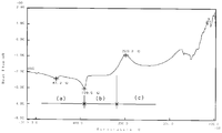
도 7에는, 나일론계의 상기 접착용 수지의 온도 상승과 상태 변화의 관계가 나타내어져 있다. 가로축은 가열 온도이고, 세로축은 열 변화를 나타내며, 세로축의 플러스측은 발열 반응을 나타내고, 마이너스측은 흡열 반응을 나타내고 있다.Fig. 7 shows the relationship between the temperature rise and the state change of the nylon-based adhesive resin. The horizontal axis represents the heating temperature, the vertical axis represents the thermal change, the plus side of the vertical axis represents the exothermic reaction, and the minus side represents the endothermic reaction.
도 7에 나타내는 (a)의 범위는, 접착용 수지를 건조시키고 있는 과정으로, 접착용 수지는 이른바 핫멜트 상태이다. 109℃ 부근까지 가열되어 용제가 증발하면, (b)의 범위에 들어가 건조 상태가 되고, 온도 상승과 함께 가교 반응이 개시된다. 또한 온도가 150℃ 또는 160℃를 초과하여 (c)의 범위가 되면, 3차원 가교가 촉진되어 수불용성이 된다.The range (a) in Fig. 7 is a process of drying the adhesive resin, and the adhesive resin is in the so-called hot-melt state. When the solvent is heated to about 109 캜 and the solvent evaporates, it falls into the range of (b) and becomes dry, and the crosslinking reaction starts with the temperature rise. When the temperature exceeds 150 占 폚 or 160 占 폚 and reaches the range of (c), the three-dimensional crosslinking is promoted and becomes insoluble in water.
상기 접착 수지층(32)은, 접착용 수지를, 금속 도체(10)를 구성하는 금속 판재의 표면에 도포하고, 도 7에 있어서 (b)에서 나타내는 범위의 온도 조건에서 가열한 상태로 사용된다. 즉 110℃∼150℃ 또는 110∼160℃의 가열 조건에서 접착용 수지가 건조된 상태로서, 완전한 가교 상태가 되어 있지 않은 가경화 상태 즉 부분 가교 상태로 사용된다. 인서트 성형법에서는, 금형 내에 사출되는 용융 수지와 접촉함으로써 접착 수지층(32)이 가열되어 용융하고, 접착 수지층(32)과 기체(3)를 형성하는 합성 수지가 상용 상태가 된다. 따라서, 성형 후의 기체(3)는 금속 도체(10)와 고착된다.The
전술과 같이, 상기 절연 수지층(31)과 접착 수지층(32)은, 서로 친화성이 있어 밀착성이 좋은 수지 재료로 형성된다. 실시형태에서는, 절연 수지층(31)이 우레탄 수지로 형성되고, 경화제에 이소시아네이트가 사용된다. 접착 수지층(32)을 형성하고 있는 나일론 수지와 우레탄 수지는 화학적 구조가 근사한 것이 알려져 있고, 게다가 절연 수지층(31)과 접착 수지층(32)에서 동일한 이소시아네이트계의 경화제를 사용하고 있다. 절연 수지층(31)과 접착 수지층(32)으로서 상기 수지를 선택함으로써 수지층간의 밀착성이 좋아진다.As described above, the insulating
절연 수지층(31)은, 접착 수지층(32)과 같은 가경화 상태가 아니라, 3차원 가교가 촉진되어 대략 불용성이 된 상태로 형성된다. 즉, 상기 접착 수지층(32)은 가교의 정도가 낮은 가경화의 상태로 형성되나, 절연 수지층(31)은, 접착 수지층(32)보다 3차원 가교가 촉진된 것이 사용된다. 그 때문에, 절연 수지층(31)은 접착 수지층(32)보다 높은 온도에서 가열 처리되어 사용된다. 절연 수지층(31)의 가열 처리 온도는 예를 들면 180℃ 이상이 바람직하다. 인서트 성형법에서는, 전술과 같이 접착 수지층(32)이 기체(3)를 구성하는 합성 수지와 상용 상태가 되나, 절연 수지층(31)은, 기체(3)를 구성하는 합성 수지와 완전한 상용 상태가 되기는 어려워, 절연 수지층(31)으로서 금속 도체(10)의 표면에 남게 된다.The insulating
도 8은, 금속 도체(10)가 인서트된 기체(3)의 일부 단면을 촬영한 전자 현미경 사진이다. 금속 도체(10)는, 표면을 진공 자외광 조사로 활성화 처리한 후에 절연 수지층(31)을 형성하고, 또한 절연 수지층(31)의 표면을 진공 자외광 조사로 활성화시켜 접착 수지층(32)을 형성한 것이다. 이 사진은 50,000배이다. 도 8에서는 10이 금속 도체, 10a가 도금층이다. 도금층(10a)의 표면에 절연 수지층(31)이 밀착하고, 또한 접착 수지층(32)이 기체(3)의 합성 수지와 상용 상태가 되어 있는 구조가 나타내어져 있다.Fig. 8 is an electron microscope photograph of a part of the cross-section of the
인서트 성형 후의 기체(3)에서는, 금속 도체(10)의 제 1 판부(11)의 2개의 표면(11a, 11b)에 형성된 접착 수지층(32)이, 기체(3)를 구성하는 합성 수지와 상용 상태가 되어 있고, 제 2 판부(12)의 2개의 표면(12a, 12b)에 형성된 접착 수지층(31)이, 기체(3)를 구성하는 합성 수지와 상용 상태가 되어 있다. 그 때문에, 금속 도체(10)와 기체(3)의 저벽부(3a)와의 밀착부에 간극이 형성되기 어려워져, 도 2에 나타내는 하우징(2)의 내부의 수납 공간(5)의 기밀성을 높일 수 있다.The
금속 도체(10)에서는, 제 1 판부(11)와 제 2 판부(12)의 경계의 굴곡부(15)의 양면에도 접착 수지층(32)이 형성되어 있기 때문에, 이 굴곡부(15)에 있어서도, 금속 도체(10)와 기체(3)를 구성하고 있는 합성 수지를 강고하게 고착시킬 수 있다.Since the
굴곡부(15)를 가지는 금속 도체(10)를 이용한 인서트 성형법에서는, 굴곡부(15)의 주위에서 용융 수지의 흐름이 나빠지기 때문에, 수지가 냉각되어 고체화될 때에, 굴곡부(15)의 주위에 싱크 마크라고 불리는 변형이 발생하기 쉬워진다. 또한, 저벽부(3a)가 얇으면, 굴곡부(15)가 매설되어 있는 부분에서 수지 강도가 저하되기 쉽다. 그러나, 굴곡부(15)를 사이에 두는 양측에 위치하는 제 1 판부(11)와 제 2 판부(12)의 양면에 접착 수지층(32)이 설치되고, 추가로 굴곡부(15)의 표면에도 접착 수지층(32)이 설치되어 있기 때문에, 굴곡부(15)를 포함하는 영역에서 금속 도체(10)와 기체(3)가 강고하게 고착되게 되어, 싱크 마크의 문제나 강도 저하의 문제가 생기기 어려워진다.In the insert molding method using the
도 4에 나타내는 바와 같이, 기체(3)로부터 외부 단자부(14)가 돌출되어 있는 부분에서는, 제 1 판부(11)의 2개의 표면(11a, 11b)에 형성된 접착 수지층(32)이 기체(3)를 구성하는 수지와 상용 상태가 되어, 제 1 판부(11)와 기체(3)가 강고하게 고착되어 있다. 따라서, 외부 단자부(14)의 돌출 기부(基部)에 있어서, 금속 도체(10)와 기체(3)의 사이에 간극이 형성되는 경우가 없어, 수납 공간(5)의 기밀성을 높은 상태로 유지할 수 있다. 또한, 외부 단자부(14)의 돌출 기부의 주위에서의 기체(3)의 강도를 높일 수도 있다.4, the
도 3에 나타내는 구분 (ⅲ)에서는, 내부 단자부(13)의 하측 표면(13a)이 접착 수지층(32)에 의해 기체(3)를 구성하는 합성 수지에 고착시켜져 있다. 한편, 도 6에도 나타내는 바와 같이, 내부 단자부(13)의 상측 표면(13b)은 저벽부(3a)로부터 노출되어 있다. 이 상측 표면(13b)에는 절연 수지층(31)이나 접착 수지층(32)이 형성되어 있지 않고, 진공 자외광을 사용한 상기 활성화 처리가 실시되어 있지 않은 상태이며, 은 도금이 황화 방지제 등의 보호제로 덮인 채이다.3, the
구분 (ⅳ)에서는, 외부 단자부(14)가 기체(3)의 측방으로 돌출되어 있으나, 외부 단자부(14)의 상측 표면(14a)과 하측 표면(14b)에도 절연 수지층(31)이나 접착 수지층(32)이 형성되어 있지 않고, 진공 자외광을 사용한 상기 활성화 처리도 실시되어 있지 않다. 따라서, 표면(14a, 14b)은 은 도금이 황화 방지제 등의 보호제로 덮인 채이다.In the category (iv), the external
따라서, 내부 단자부(13)의 상측 표면(13b)과, 외부 단자부(14)의 하측 표면(14a) 및 상측 표면(14b)은, 은 도금이 부식되기 어려운 상태를 유지할 수 있다.The
도 5와 도 6에 나타내는 바와 같이, 기체(3)를 인서트 성형하는 공정에서는, 금형 내에 있어서, 제 1 판부(11)의 하측 표면(11a)이 지지 돌출체(21)에 맞닿아 지지되고, 내부 단자부(13)의 하측 표면(13a)도 지지 돌출체(22)에 맞닿아 지지된 상태에서, 금형 및 지지 돌출체(21, 22)가 가열된다. 이때, 지지 돌출체(21, 22)가 맞닿아 있는 부분에서 가경화 상태의 접착 수지층(32)이 용융하여, 지지 돌출체(21, 22)가 맞닿는 부분에서 접착 수지층(32)이 제거된다. 또한, 접착 수지층(32)은, 도 7에 나타내는 (b)의 범위에서 가열 처리되어 있고, (a)의 범위의 핫멜트 상태에 비해 점착성이 저하되어 있다. 그 때문에, 용융한 접착 수지층(32)은 지지 돌출체(21, 22)의 선단면(先端面) 등에 부착되기 어렵다.5 and 6, in the step of insert molding the
한편, 절연 수지층(31)은 3차원 가교 상태로 형성되어 있기 때문에, 금형 온도에 의해 용해되는 경우가 없어, 지지 돌출체(21, 22)가 맞닿는 부분에 있어서도, 금속 도체(10)의 표면이 절연 수지층(31)으로 덮인 상태로 유지된다.On the other hand, since the insulating
인서트 성형 후의 기체(3)에서는, 도 2와 도 3에 나타내는 바와 같이, 기체(3)의 저벽부(3a)에 바닥면(3c)으로부터 금속 도체(10)로 통하는 개구부(3d, 3e)가 복수 개소에 형성된다. 도 5와 도 6에 나타내는 바와 같이, 개구부(3d, 3e)의 주위에서는, 접착 수지층(32)과 기체(3)를 구성하는 수지가 상용 상태가 되고 나서 경화하기 때문에, 개구부(3d, 3e)의 주위의 전체 둘레에 있어서, 금속 도체(10)와 기체(3)가 밀착하여 고착된다. 그 때문에, 이 주위 부분에 간극이 형성되는 경우가 없어져, 수납 공간(5) 내의 기밀성을 더 높일 수 있다.In the
또한, 저벽부(3a)의 바닥면(3c)에 개구하는 개구부(3d, 3e)의 내부에 금속 도체(10)가 노출되나, 도 5와 도 6에 나타내는 바와 같이, 개구부(3d, 3e)의 내부에서, 금속 도체(10)의 표면이 절연 수지층(31)으로 덮여 있기 때문에, 금속 도체(10)의 절연이 유지되어 있다.The
하우징(2)은 1변이 5㎜ 이하 나아가서는 2㎜ 이하의 미소한 입방체이기 때문에, 기체(3)의 바닥면(3c)에 수분이 부착되는 경우가 있으면, 수분이 복수 개소의 개구부(3d, 3e)에 동시에 들어가기 쉬워진다. 그러나, 개구부(3d, 3e)의 바닥부에 드러나 있는 금속 도체(10)의 표면이 절연 수지층(31)으로 덮여 절연되어 있기 때문에, 수분에 의해 금속 도체(10)끼리가 단락하는 것을 방지할 수 있다.Since the
또한, 상기 실시형태에서는, 기체(3)를 구성하는 합성 수지를 나일론 9T, 접착 수지층(32)을 구성하는 접착용 수지를 나일론 수지, 절연 수지층(31)을 형성하는 수지를 우레탄 수지로 하여 설명하였으나, 이들 수지는 서로 상용성이나 친화성이 있으면 상기 조합에 한정되지 않는다. 예를 들면, 우레탄계-우레탄계, 아크릴계-아크릴계, 올레핀계-올레핀계, 에폭시계-에폭시계, 이소시아네이트계-이소시아네이트계 등의 동일계 등의 재료 외에, 에폭시계-우레탄계, 우레탄계-이소시아네이트계, 에폭시계-이소시아네이트계 등의 조합이 가능하다. 또한, 극성화를 촉진하는 활성화 처리는 진공 자외광의 조사에 한정되는 것은 아니고, 플라즈마 처리, UV 오존 처리, 코로나 처리, 화성 처리, 화염 처리, 가열 처리, 양극 산화 처리 등이어도 된다.In the above embodiment, the nylon 9T is used as the synthetic resin constituting the
다음에, 상기 전자부품(1)의 제조 방법에 대하여 설명한다.Next, a manufacturing method of the
도 12에는, 금속 도체(10)가 매설된 기체(3)가 성형될 때까지의 제조 방법이 공정순으로 나타내어져 있다.In Fig. 12, the manufacturing method until the
도 12에 나타내는 P1(프로세스 1)의 공정에서 마스크가 제조된다. 마스크는, 도 9에 나타내는 제 1 마스크 시트(40A)와 도 10에 나타내는 제 2 마스크 시트(40B)의 2종류가 제조된다. 제 1 마스크 시트(40A)는, 금속 도체(10)의 하측 표면(11a, 13a) 및 좌측 표면(12a)에 절연 수지층(31)과 접착 수지층(32)을 형성하기 위한 것이고, 제 2 마스크 시트(40B)는, 금속 도체(10)의 상측 표면(11b)과 우측 표면(12b)에 접착 수지층(32)을 형성하기 위한 것이다.A mask is manufactured in the process of P1 (process 1) shown in Fig. As the mask, two types of the
도 12의 P2의 공정에서는, 후프 기재가 되는 금속 판재(50)와 마스크 시트(40A, 40B)가 맞붙여진다.In the step P2 of Fig. 12, the
도 9에는, 금속 판재(50)의 하측 표면(50a)에 제 1 마스크 시트(40A)가 포개진 상태가 평면도로 나타내어져 있다. 도 11(A)에는, 금속 판재(50)의 하측 표면(50a)에 제 1 마스크 시트(40A)가 맞붙여진 상태가 단면도로 나타내어져 있다. 제 1 마스크 시트(40A)와 금속 판재(50)는, 점착제에 의해 서로 위치 어긋나지 않도록 맞붙여진다.9 shows a state in which the
도 9에서는, 금속 판재(50)를 프레스 가공에 의해 절단하여, 4개의 금속 도체(10)를 잘라내기 위한 절단 예정선(52)이 파선으로 나타내어져 있다. 금속 판재(50)는 인청동판의 양표면에 은 도금이 실시되고, 은 도금의 표면에 황화 방지 등을 위한 보호제가 도포된 것이다. 또한, 금속 판재(50)에는 인서트 성형의 금형(20) 내로 보내기 위한 이송용 구멍(51)이 일정한 간격으로 형성되어 있다.In Fig. 9, the
마스크는 PET(폴리에틸렌·테레프탈레이트) 필름 등의 수지 필름으로 제조된다. 도 9에 나타내는 바와 같이, 제 1 마스크 시트(40A)에는, 도 3에 나타내는 금속 도체(10)의 구분 (i)에 대응하는 4개의 마스크 개구부(41)가 형성되어 있고, 절단 예정선(52)으로 절단되는 금속 도체(10)의 일부에, 각각의 마스크(1)가 포개져 있다.The mask is made of a resin film such as a PET (polyethylene terephthalate) film. 9, four
도 10에는, 금속 판재(50)의 상측 표면(50b)에 제 2 마스크 시트(40B)가 포개진 상태가 나타내어져 있다. 제 2 마스크 시트(40B)에는 마스크 개구부(42)가 형성되어 있다. 마스크 개구부(42)는, 도 3에 나타내는 금속 도체(10)의 구분 (ⅱ)에 대응하는 것이고, 제 2 마스크 시트(40B)가 상측 표면(50b)에 맞붙여지면, 각각의 마스크 개구부(42)가, 금속 도체(10)가 되는 부분에 포개진다.In Fig. 10, a state in which the
도 12에 나타내는 P3의 공정에서는, 금속 판재(50)의 하측 표면(50a)과 상측 표면(50b)에 대해 부분적으로 극성화를 촉진하기 위한 활성화 처리가 행하여진다.In the step of P3 shown in Fig. 12, an activation process is performed to promote partial polarization of the
활성화 처리는, 도 9에 나타내는 제 1 마스크 시트(40A)의 마스크 개구부(41) 내에 노출되어 있는 금속 판재(50)의 하측 표면(50a)에 대해, 진공 자외광을 조사함으로써 행하여진다. 마찬가지로, 도 10에 나타내는 제 2 마스크 시트(40B)의 마스크 개구부(42) 내에 노출되어 있는 상측 표면(50b)에 대해, 진공 자외광을 조사하여 활성화 처리가 행하여진다.The activation process is performed by irradiating vacuum ultraviolet light onto the
활성화 처리에서는, 파장이 172㎚인 엑시머광을 사용하여, 금속 판재(50)의 표면(50a, 50b)에 대해 10∼15㎽의 광원을 5㎜ 이하 바람직하게는 3㎜ 정도의 거리로 가까이 하여 10초 정도 조사한다. 진공 자외광이 조사되면, 금속 표면의 산소가 분해시켜지는 등하여 극성이 촉진된다. 활성화 처리 후의 금속 표면의 표면 자유 에너지는 35mJ/㎡ 이상인 것이 바람직하다. 상한은 특별히 범위를 마련할 필요는 없으나, 50mJ/㎡∼300mJ/㎡ 정도이다.In the activation process, the excimer light having a wavelength of 172 nm is used to irradiate the light sources of 10 to 15 mW to the
도 12에 나타내는 P4의 공정에서는, 도 9에 나타내는 제 1 마스크 시트(40A)의 마스크 개구부(41)로부터 노출되어 있는 금속 판재(50)의 하측 표면(50a)에, 절연 수지층(31)을 형성한다. 전술과 같이 절연 수지층(31)을 구성하는 수지 재료는, 우레탄 수지에 이소시아네이트의 경화제가 혼합된 것이다. P5의 공정에서는, 수지 재료를 저온의 가열 조건하에서 가건조(假乾燥)시키고, 그 후의 P6의 공정에서, 예를 들면 180℃ 이상의 온도에서 가열하고, 3차원 가교시켜 경화시키고, 절연 수지층(31)의 성형을 완료한다.12, the insulating
도 12의 P7의 공정에서는, 경화한 절연 수지층(31)의 표면에 진공 자외광을 조사하여, 절연 수지층(31)의 표면의 극성화를 촉진시킨다.12, the surface of the cured insulating
도 12의 P8의 공정에서는, 절연 수지층(31)의 표면에 접착 수지층(32)을 형성한다. 전술과 같이, 접착 수지층(32)을 형성하기 위한 접착용 수지는, 나일론의 주제와 이소시아네이트의 경화제의 2액 혼합 타입이 사용된다. 도 12의 P9의 공정에서 접착용 수지가 가건조되고, P10의 공정에서 가열 처리된다. 도 7에 의거하여 이미 설명한 바와 같이, 접착용 수지는 인쇄 후에 110∼150℃ 또는 110∼160℃의 범위에서 가열 처리하고, 3차원 가교가 완전히 진행되어 있지 않은 가경화 상태로 하여 접착 수지층(32)이 형성된다.In the step of P8 in Fig. 12, the
도 12의 P8의 공정, P9의 공정, P10의 공정에서는, 도 10에 나타내는 금속 판재(50)의 상측 표면(50b)에 대해서도 접착 수지층(32)이 형성된다. 상측 표면(50b)에는 절연 수지층(31)은 형성되지 않고, P3의 공정에서 진공 자외광 처리가 행하여진 후에, 절연 수지층(31)이 형성된다.In step P8, step P9, and step P10 in Fig. 12, an
P11의 공정에서는, 제 1 마스크 시트(40A)와 제 2 마스크 시트(40B)가 금속 판재(50)로부터 박리된다.In the process of P11, the
도 11(A)에서는, 금속 판재(50)와 제 1 마스크 시트(40A)가 맞붙여진 상태에서, 절연 수지층(31)과 접착 수지층(32)이 포개어 형성된 상태가 나타내어져 있다. 도 11(B)에 나타내는 바와 같이, 제 1 마스크 시트(40A)가 금속 판재(50)로부터 박리되면, 마스크 개구부(42)가 형성되어 있었던 영역에 수지층(31, 32)이 형성된다. 금속 도체(10)의 길이는 1㎜ 미만으로 수지층(31, 32)이 형성되는 영역의 면적이 미소하나, 금속 판재(50)의 하측 표면(50a)에서는, 마스크 개구부(42)의 내부에서 진공 자외광에 의한 활성화 처리가 행하여져 젖음성이 향상되어 있기 때문에, 제 1 마스크 시트(40A)가 벗겨질 때에, 마스크 개구부(41) 내의 수지층(31, 32)이 함께 벗겨지는 경우는 없다.11A shows a state in which the insulating
마찬가지로, 도 10에 나타내는 제 2 마스크 시트(40B)가 금속 판재(50)의 상측 표면(50b)으로부터 벗겨지고, 제 2 마스크 시트(40B)의 마스크 개구부(42)가 형성되어 있는 부분에 접착 수지층(32)이 형성된다.Similarly, the
도 12의 P12의 공정에서는, 금속 판재(50)의 하측 표면(50a)에 절연 수지층(31)과 접착 수지층(32)이 형성되고, 상측 표면(50b)에 접착 수지층(32)이 형성된 후에, 프레스 공정으로 이행한다. 프레스 공정에서는, 도 9와 도 10에 나타내는 절단 예정선(52)으로 금속 판재(50)가 절단된다. 절단 후에는, 좌우 양측의 반송 후프부(53, 53)의 내측에 좌우 2조각씩의 금속 도체(10)가 일체로 연결된 상태가 된다. 또한, 벤딩 가공에 의해, 각각의 금속 도체(10)가, 도 2와 도 3에 나타내는 입체 형상으로 벤딩 성형된다.12, the insulating
도 12에 나타내는 P13의 공정의 인서트 성형에서는, 반송 후프부(53, 53)와 일체인 금속 도체(10)가, 도 5와 도 6에 일부만이 나타내어져 있는 금형(20)의 내부에 공급되고, 금속 도체(10)의 제 1 판부(11)가 지지 돌출체(21)로 지지되고, 내부 단자부(13)가 지지 돌출체(22)로 지지된다. 그리고, 금형(20)의 캐비티 내에 용융 수지가 사출되어, 기체(3)가 성형된다.12, the
또한, 판부(11)의 측면은, 프레스 공정에서 금속 도체(10)의 절단면이 노출된 부분으로, 접착 수지층(32)이 존재하지 않으나, 용융 수지 사출시의 열에 의해 접착 수지층(32)이 연화되어, 용융 수지의 압력에 의해 판부(11)의 측면으로 돌아 들어가 고착, 밀봉되기 때문에, 이 부분에 간극이 형성되는 경우가 없어, 수납 공간(5) 내의 기밀성이 손상되는 경우는 없다.The side surface of the
기체(3)가 형성된 후에, 반송 후프부(53, 53)로부터 금속 도체(10)가 절단되어 분리되고, 도 1과 도 2에 나타내는 전자부품이 완성된다.After the
상기 제조 방법에서는, 도 9와 도 10에 나타내는 바와 같이, 금속 판재(50)의 하측 표면(50a)과 상측 표면(50b)이 평면인 상태에서, 진공 자외광 처리와, 수지층(31, 32)의 성형 공정이 행하여지고, 그 후에 절단으로 벤딩 성형을 행하여 입체 형상의 금속 도체(10)가 형성된다. 그 때문에, 벤딩 성형된 후의 제 1 판부(11)와 제 2 판부(12)나, 굴곡부(15)의 양표면에 수지층을 형성할 수 있어, 이들 부분과 기체(3)의 고착 강도를 높일 수 있다. 특히, 예를 들면 전체 길이가 1㎜ 미만의 미소한 금속 도체(10)라도, 굴곡부나 입체 형상 부분에 절연 수지층(31)이나 접착 수지층(32)을 형성할 수 있다.9 and 10, the vacuum ultraviolet light treatment and the resin layers 31 and 32 (see FIG. 9) are performed while the
또한, 도 12에 나타내는 제조 방법에서는 P3 내지 P10까지의 공정에서 동일한 마스크가 사용되고 있으나, 예를 들면 P4의 공정에 있어서의 절연 수지층(31)의 성형과 P8의 공정에 있어서의 접착 수지층(32)의 성형에서 다른 마스크를 사용해도 된다.12, the same mask is used in the processes from P3 to P10. For example, in the process of forming the insulating
1 : 전자부품
2 : 하우징
3 : 기체
3a : 저벽부
3d, 3e : 개구부
5 : 수납 공간
6 : 검지 소자
10 : 금속 도체
11 : 제 1 판부
11a : 하측 표면
11b : 상측 표면
12 : 제 2 판부
12a : 좌측 표면
12b : 우측 표면
13 : 내부 단자부
13a : 하측 표면
13b : 상측 표면
14 : 외부 단자부
15 : 굴곡부
20 : 금형
21, 22 : 지지 돌출체
31 : 절연 수지층
32 : 접착 수지층
40A : 제 1 마스크 시트
40B : 제 2 마스크 시트
41, 42 : 개구부
50 : 금속 판재
50a : 하측 표면
50b : 상측 표면
52 : 절단 예정선
53 : 반송 후프부1: Electronic parts
2: Housing
3: Gas
3a:
3d, 3e: opening
5: Storage space
6: Detector
10: metal conductor
11: first plate
11a: lower surface
11b: upper surface
12: second plate
12a: Left surface
12b: right surface
13: internal terminal portion
13a: Lower surface
13b: upper surface
14: external terminal portion
15: Bend
20: Mold
21, 22: support protrusion body
31: Insulating resin layer
32: Adhesive resin layer
40A: first mask sheet
40B: second mask sheet
41, 42: opening
50: metal plate
50a: lower surface
50b: upper surface
52: Line to be cut
53: conveying hoop portion
Claims (10)
(2) 상기 활성화 처리를 실시한 영역에 접착 수지층을 형성하는 공정과,
(3) 상기 (1), (2)의 공정 후에, 상기 금속 판재로부터, 적어도 일부에 상기 접착 수지층을 가지는 상기 금속 도체의 잘라냄과 벤딩 가공을 행하는 공정과,
(4) 상기 금속 도체를 금형 내에 설치하고 합성 수지를 상기 금형 내에 사출하여 상기 기체를 성형하는 공정을 가지는 것을 특징으로 하는 전자부품의 제조 방법.1. A method of manufacturing an electronic component for forming a base made of a synthetic resin by inserting a metal conductor, the method comprising the steps of: (1) partially activating a surface of a metal plate;
(2) a step of forming an adhesive resin layer in the region subjected to the activation treatment,
(3) a step of cutting and bending the metal conductor having the adhesive resin layer at least partially from the metal plate after the steps (1) and (2)
(4) A method for manufacturing an electronic part, comprising the step of providing the metal conductor in a metal mold and injecting a synthetic resin into the metal mold to mold the metal body.
상기 (1)의 공정과 (2)의 공정의 사이에,
(1a) 상기 활성화 처리를 실시한 영역에 절연 수지층을 형성하는 공정과,
(1b) 상기 절연 수지층의 표면의 적어도 일부에, 제 2 활성화 처리를 실시하는 공정이 포함되고,
상기 (2)의 공정에서는, 상기 제 2 활성화 처리를 실시한 상기 절연 수지층의 위에 상기 접착 수지층을 형성하는, 전자부품의 제조 방법.The method according to claim 1,
Between the step of (1) and the step of (2)
(1a) forming an insulating resin layer in the region subjected to the activation treatment,
(1b) A step of performing a second activation treatment on at least a part of the surface of the insulating resin layer,
In the step (2), the adhesive resin layer is formed on the insulating resin layer subjected to the second activation treatment.
상기 금속 판재에 포개진 동일한 마스크를 사용하여, 상기 (1)과 (2)의 처리가 행하여지는 전자부품의 제조 방법.The method according to claim 1,
(1) and (2) are performed by using the same mask embedded in the metal plate material.
상기 금속 판재에 포개진 동일한 마스크를 사용하여, 상기 (1)과 (1a), (1b) 및 (2)의 처리가 행하여지는 전자부품의 제조 방법.3. The method of claim 2,
(1), (1a), (1b) and (2) are performed by using the same mask embedded in the metal plate.
상기 (4)의 공정에서는, 상기 금형 내에 설치된 상기 금속 도체의 상기 절연 수지층이 형성되어 있는 부분을 지지 돌출체로 지지하여, 기체의 성형을 행하는 전자부품의 제조 방법.The method according to claim 2 or 4,
In the step (4), a portion of the metal conductor provided in the metal mold, on which the insulating resin layer is formed, is supported by the support protrusion to mold the base body.
상기 (2)에서 형성되는 상기 접착 수지층과, 상기 (4)의 사출 성형에서 사용되는 합성 수지가, 상용성을 가지는 전자부품의 제조 방법.6. The method according to any one of claims 1 to 5,
Wherein the adhesive resin layer formed in the step (2) and the synthetic resin used in the injection molding in the step (4) have compatibility.
상기 (2)에서 형성되는 상기 접착 수지층은, 상기 (1a)에서 형성되는 절연 수지층보다 가교의 정도가 낮은 가경화의 상태에서, 상기 (3), (4)의 공정으로 이행하는 전자부품의 제조 방법.The method according to any one of claims 2, 4, and 5,
The adhesive resin layer formed in the step (2) is a part of the electronic component to be transferred to the steps (3) and (4) in the state of the low-hardening state where the degree of bridging is lower than that of the insulating resin layer formed in (1a) ≪ / RTI >
상기 활성화 처리는, 진공 자외광을 조사하는 극성화 처리인 전자부품의 제조 방법.8. The method according to any one of claims 1 to 7,
Wherein the activation treatment is a polarizing treatment for irradiating vacuum ultraviolet light.
상기 (2)의 공정에서는, 금속 도체에 있어서의 기체에 매설되는 부분의 양표면에 상기 접착 수지층을 형성하는 전자부품의 제조 방법.9. The method according to any one of claims 1 to 8,
In the step (2), the adhesive resin layer is formed on both surfaces of a portion buried in the base of the metal conductor.
상기 금속 도체는, 그 일부가 상기 기체로부터 돌출하여 단자부가 되어 있고, 상기 단자부에는, 상기 (1)의 활성화 처리를 실시하지 않는 전자부품의 제조 방법.10. The method according to any one of claims 1 to 9,
Wherein the metal conductor is partly protruded from the base to form a terminal portion, and the terminal portion is not subjected to the activation treatment of (1).
Applications Claiming Priority (3)
| Application Number | Priority Date | Filing Date | Title |
|---|---|---|---|
| JPJP-P-2014-078239 | 2014-04-04 | ||
| JP2014078239 | 2014-04-04 | ||
| PCT/JP2015/060444 WO2015152364A1 (en) | 2014-04-04 | 2015-04-02 | Method for manufacturing electronic component |
Publications (2)
| Publication Number | Publication Date |
|---|---|
| KR20160129068A true KR20160129068A (en) | 2016-11-08 |
| KR101950899B1 KR101950899B1 (en) | 2019-05-10 |
Family
ID=54240672
Family Applications (1)
| Application Number | Title | Priority Date | Filing Date |
|---|---|---|---|
| KR1020167027284A KR101950899B1 (en) | 2014-04-04 | 2015-04-02 | Method for manufacturing electronic component |
Country Status (4)
| Country | Link |
|---|---|
| JP (1) | JP6214757B2 (en) |
| KR (1) | KR101950899B1 (en) |
| CN (1) | CN106132660A (en) |
| WO (1) | WO2015152364A1 (en) |
Families Citing this family (2)
| Publication number | Priority date | Publication date | Assignee | Title |
|---|---|---|---|---|
| US9868632B2 (en) * | 2016-03-24 | 2018-01-16 | Infineon Technologies Ag | Molded cavity package with embedded conductive layer and enhanced sealing |
| CN110248792A (en) * | 2017-02-03 | 2019-09-17 | 宝理塑料株式会社 | The joint method of synthetic resin |
Citations (6)
| Publication number | Priority date | Publication date | Assignee | Title |
|---|---|---|---|---|
| JPH05114664A (en) * | 1991-05-31 | 1993-05-07 | Toshiba Chem Corp | Manufacture of electronic equipment case |
| JPH0629021U (en) | 1992-09-21 | 1994-04-15 | アルプス電気株式会社 | Terminal mounting structure for electrical parts |
| JPH09252184A (en) * | 1996-03-18 | 1997-09-22 | Fujitsu Ltd | Housing and manufacturing method thereof |
| JPH1055906A (en) | 1996-08-12 | 1998-02-24 | Alps Electric Co Ltd | Hermetic structure of electronic component |
| JP2013071452A (en) * | 2011-09-27 | 2013-04-22 | Ichia Technologies Inc | Method for bonding plastic molding member to metal housing |
| JP5234011B2 (en) * | 2010-01-07 | 2013-07-10 | 豊田合成株式会社 | Method for producing composite of metal and resin |
Family Cites Families (7)
| Publication number | Priority date | Publication date | Assignee | Title |
|---|---|---|---|---|
| JPS63184357A (en) * | 1987-01-26 | 1988-07-29 | Japan Aviation Electronics Ind Ltd | Method for molding and holding terminal |
| JP2000150551A (en) * | 1998-11-11 | 2000-05-30 | Orc Mfg Co Ltd | Mechanism and method for surface treating lead frame |
| US6214152B1 (en) * | 1999-03-22 | 2001-04-10 | Rjr Polymers, Inc. | Lead frame moisture barrier for molded plastic electronic packages |
| JP2001315159A (en) * | 2000-05-10 | 2001-11-13 | Mitsubishi Plastics Ind Ltd | Method for manufacturing injection molding having metal plate |
| JP3947533B2 (en) * | 2004-07-16 | 2007-07-25 | 吉川工業株式会社 | Plastic hollow package for semiconductor storage |
| JP5499741B2 (en) * | 2010-02-04 | 2014-05-21 | 三菱樹脂株式会社 | Resin / metal laminate, resin / metal composite injection molded body, and method for producing the same |
| SG190948A1 (en) * | 2010-12-02 | 2013-07-31 | Toray Industries | Method for producing metal composite, and chassis for electronic equipment |
-
2015
- 2015-04-02 CN CN201580014133.7A patent/CN106132660A/en active Pending
- 2015-04-02 WO PCT/JP2015/060444 patent/WO2015152364A1/en active Application Filing
- 2015-04-02 JP JP2016511996A patent/JP6214757B2/en active Active
- 2015-04-02 KR KR1020167027284A patent/KR101950899B1/en active IP Right Grant
Patent Citations (6)
| Publication number | Priority date | Publication date | Assignee | Title |
|---|---|---|---|---|
| JPH05114664A (en) * | 1991-05-31 | 1993-05-07 | Toshiba Chem Corp | Manufacture of electronic equipment case |
| JPH0629021U (en) | 1992-09-21 | 1994-04-15 | アルプス電気株式会社 | Terminal mounting structure for electrical parts |
| JPH09252184A (en) * | 1996-03-18 | 1997-09-22 | Fujitsu Ltd | Housing and manufacturing method thereof |
| JPH1055906A (en) | 1996-08-12 | 1998-02-24 | Alps Electric Co Ltd | Hermetic structure of electronic component |
| JP5234011B2 (en) * | 2010-01-07 | 2013-07-10 | 豊田合成株式会社 | Method for producing composite of metal and resin |
| JP2013071452A (en) * | 2011-09-27 | 2013-04-22 | Ichia Technologies Inc | Method for bonding plastic molding member to metal housing |
Also Published As
| Publication number | Publication date |
|---|---|
| CN106132660A (en) | 2016-11-16 |
| KR101950899B1 (en) | 2019-05-10 |
| WO2015152364A1 (en) | 2015-10-08 |
| JPWO2015152364A1 (en) | 2017-04-13 |
| JP6214757B2 (en) | 2017-10-18 |
Similar Documents
| Publication | Publication Date | Title |
|---|---|---|
| US7240847B2 (en) | Chip card | |
| TWI619417B (en) | Portable electronic device and method of manufacturing the same | |
| US20200350723A1 (en) | Connector and manufacturing method therefor | |
| JP2006303327A (en) | Electronic circuit device and its manufacturing method | |
| KR101950899B1 (en) | Method for manufacturing electronic component | |
| KR20160111389A (en) | Electronic functional component and method for producing an electronic functional component | |
| US20170324235A1 (en) | Molded part-equipped electrical cable | |
| JP6341508B2 (en) | Waterproof connector and method for manufacturing waterproof connector | |
| CN111755890B (en) | Connector device | |
| US11005151B2 (en) | Radome for vehicles and method for manufacturing said radome | |
| US11904506B2 (en) | Connector and method for manufacturing same | |
| KR101730994B1 (en) | Electronic component | |
| JP2020092013A (en) | Connector and manufacturing method of the same | |
| KR101730997B1 (en) | Electronic component | |
| CN113675044A (en) | Process for manufacturing sealed automotive electrical fuse box | |
| CN109638333B (en) | Insert molding method and insert molded part | |
| KR101315116B1 (en) | Manufacturing method for film antenna | |
| KR20070099407A (en) | Method for packaging flash memory cards | |
| US10973137B2 (en) | Circuit device, method for manufacturing circuit device and connector | |
| KR20160134685A (en) | Electronic control module and method for producing the same | |
| JP2003094479A (en) | Semiconductor device and its manufacturing method | |
| JP6950796B2 (en) | Battery module manufacturing method | |
| WO2016208114A1 (en) | Resin molded article and method for producing same | |
| JP6358075B2 (en) | Resin molded body and manufacturing method thereof | |
| JP6277780B2 (en) | Manufacturing method of resin molding |
Legal Events
| Date | Code | Title | Description |
|---|---|---|---|
| A201 | Request for examination | ||
| E902 | Notification of reason for refusal | ||
| AMND | Amendment | ||
| E601 | Decision to refuse application | ||
| AMND | Amendment | ||
| X701 | Decision to grant (after re-examination) |