KR20160108423A - Analog behavior modeling for 3-phase signaling - Google Patents
Analog behavior modeling for 3-phase signaling Download PDFInfo
- Publication number
- KR20160108423A KR20160108423A KR1020167021576A KR20167021576A KR20160108423A KR 20160108423 A KR20160108423 A KR 20160108423A KR 1020167021576 A KR1020167021576 A KR 1020167021576A KR 20167021576 A KR20167021576 A KR 20167021576A KR 20160108423 A KR20160108423 A KR 20160108423A
- Authority
- KR
- South Korea
- Prior art keywords
- voltage level
- state
- voltage
- physical connection
- signal
- Prior art date
Links
Images


Classifications
-
- G—PHYSICS
- G01—MEASURING; TESTING
- G01R—MEASURING ELECTRIC VARIABLES; MEASURING MAGNETIC VARIABLES
- G01R31/00—Arrangements for testing electric properties; Arrangements for locating electric faults; Arrangements for electrical testing characterised by what is being tested not provided for elsewhere
- G01R31/28—Testing of electronic circuits, e.g. by signal tracer
- G01R31/2832—Specific tests of electronic circuits not provided for elsewhere
- G01R31/2836—Fault-finding or characterising
- G01R31/2846—Fault-finding or characterising using hard- or software simulation or using knowledge-based systems, e.g. expert systems, artificial intelligence or interactive algorithms
- G01R31/2848—Fault-finding or characterising using hard- or software simulation or using knowledge-based systems, e.g. expert systems, artificial intelligence or interactive algorithms using simulation
-
- H—ELECTRICITY
- H04—ELECTRIC COMMUNICATION TECHNIQUE
- H04B—TRANSMISSION
- H04B17/00—Monitoring; Testing
-
- H—ELECTRICITY
- H04—ELECTRIC COMMUNICATION TECHNIQUE
- H04L—TRANSMISSION OF DIGITAL INFORMATION, e.g. TELEGRAPHIC COMMUNICATION
- H04L25/00—Baseband systems
- H04L25/02—Details ; arrangements for supplying electrical power along data transmission lines
- H04L25/0264—Arrangements for coupling to transmission lines
- H04L25/0272—Arrangements for coupling to multiple lines, e.g. for differential transmission
-
- H—ELECTRICITY
- H04—ELECTRIC COMMUNICATION TECHNIQUE
- H04L—TRANSMISSION OF DIGITAL INFORMATION, e.g. TELEGRAPHIC COMMUNICATION
- H04L25/00—Baseband systems
- H04L25/38—Synchronous or start-stop systems, e.g. for Baudot code
- H04L25/40—Transmitting circuits; Receiving circuits
- H04L25/49—Transmitting circuits; Receiving circuits using code conversion at the transmitter; using predistortion; using insertion of idle bits for obtaining a desired frequency spectrum; using three or more amplitude levels ; Baseband coding techniques specific to data transmission systems
- H04L25/4917—Transmitting circuits; Receiving circuits using code conversion at the transmitter; using predistortion; using insertion of idle bits for obtaining a desired frequency spectrum; using three or more amplitude levels ; Baseband coding techniques specific to data transmission systems using multilevel codes
-
- H—ELECTRICITY
- H04—ELECTRIC COMMUNICATION TECHNIQUE
- H04M—TELEPHONIC COMMUNICATION
- H04M1/00—Substation equipment, e.g. for use by subscribers
- H04M1/02—Constructional features of telephone sets
- H04M1/0202—Portable telephone sets, e.g. cordless phones, mobile phones or bar type handsets
- H04M1/026—Details of the structure or mounting of specific components
- H04M1/0266—Details of the structure or mounting of specific components for a display module assembly
Abstract
멀티-와이어, 멀티-위상 통신 링크에서 아날로그 거동을 모델링하는 시스템, 방법들 및 장치가 설명된다. 통신 링크에서의 물리적 연결을 표현하는 디지털 신호 및 물리적 연결을 통해 송신되는 3-위상 신호를 특성화하는 가상 신호가 생성된다. 가상 신호는 물리적 연결의 하나 이상의 아날로그 특성들을 모델링하도록 구성될 수도 있다. 아날로그 특성들은 3-위상 신호를 정의하는 전압 상태들을 포함할 수도 있다. 물리적 연결의 아날로그 특성들은 3-위상 신호의 시그널링 상태들에 대응하는 적어도 3 개의 전압 상태들을 포함한다.Systems, methods and apparatus for modeling analog behavior in multi-wire, multi-phase communication links are described. A virtual signal is generated that characterizes the digital signal representing the physical connection in the communication link and the three-phase signal transmitted over the physical connection. The virtual signal may be configured to model one or more analog characteristics of the physical connection. Analog characteristics may include voltage states that define a three-phase signal. The analog properties of the physical connection include at least three voltage states corresponding to the signaling states of the three-phase signal.

Description
관련 출원들에 대한 상호 참조Cross reference to related applications
본 출원은 2014년 1월 15일자로 미국 특허청에 출원된 미국 정규 특허 출원 제14/156,329호에 대한 우선권 및 그 이익을 주장하고, 이 미국 정규 특허 출원의 전체 내용은 본 명세서에 참조로 포함된다.This application claims the benefit of and priority to U.S. Serial No. 14 / 156,329, filed on January 15, 2014, with U.S. Patent and Trademark Office, the entire contents of which are incorporated herein by reference .
분야Field
본 개시물은 일반적으로 고속 데이터 통신 인터페이스들에 관한 것으로, 더 구체적으로는, 멀티-와이어, 멀티-위상 (multi-wire, multi-phase) 데이터 통신 링크들에서의 시그널링의 모델링에 관한 것이다.BACKGROUND I. Field The present disclosure relates generally to high speed data communication interfaces, and more particularly to modeling of signaling in multi-wire, multi-phase data communication links.
셀룰러 폰들과 같은 모바일 디바이스들의 제조자들은, 상이한 제조자들을 포함하여, 다양한 소스들로부터 모바일 디바이스들의 컴포넌트들을 획득할 수도 있다. 예를 들어, 셀룰러 폰 내의 애플리케이션 프로세서는 제 1 제조자로부터 획득될 수도 있는 한편, 셀룰러 폰용 디스플레이는 제 2 제조자로부터 획득될 수도 있다. 애플리케이션 프로세서 및 디스플레이 또는 다른 디바이스는 표준-기반의 또는 사유 (proprietary) 의 물리적 인터페이스를 이용하여 상호연결될 수도 있다. 예를 들어, 디스플레이는 MIPI (Mobile Industry Processor Interface Alliance) 에 의해 특정된 디스플레이 시스템 인터페이스 (Display System Interface; DSI) 표준에 순응하는 인터페이스를 제공할 수도 있다.Manufacturers of mobile devices, such as cellular phones, may obtain components of mobile devices from a variety of sources, including different manufacturers. For example, an application processor in a cellular phone may be obtained from a first manufacturer, while a display for a cellular phone may be obtained from a second manufacturer. The application processor and display or other devices may be interconnected using a standard-based or proprietary physical interface. For example, the display may provide an interface that conforms to a Display System Interface (DSI) standard specified by the Mobile Industry Processor Interface Alliance (MIPI).
멀티-위상에서의 시그널링의 시뮬레이션은 문제가 있을 수 있다. 특히, 멀티-위상 신호의 소정의 거동들은 와이어 또는 다른 커넥터 상의 물리적 신호의 아날로그 특성들과 관련된다. 와이어의 아날로그 상태를 표현하기 위한 실수들이 이용은, 와이어 상의 신호를 표현하기 위한 다량의 데이터의 생성과 함께, 전압 상태들의 실수 표현들을 이용하여 계산들을 수행하기 위한 결과적인 과도한 프로세싱 오버헤드를 초래할 수도 있다.Simulations of signaling in multi-phase may be problematic. In particular, certain behaviors of the multi-phase signal are associated with analog characteristics of the physical signal on the wire or other connector. The use of real numbers to represent the analog state of a wire may result in the resulting excessive processing overhead for performing calculations using real representations of voltage states with the generation of large amounts of data to represent the signal on the wire have.
본 명세서에 개시된 실시형태들은 멀티-와이어 및/또는 멀티-위상 통신 링크에 대한 개선된 아날로그 거동 모델링을 가능하게 하는 시스템들, 방법들 및 장치를 제공한다. 본 명세서에서 설명된 소정의 양태들은 디지털 시뮬레이션 및 아날로그 시뮬레이션에서 응용을 찾을 수도 있다.The embodiments disclosed herein provide systems, methods, and apparatus that enable improved analog behavior modeling for multi-wire and / or multi-phase communication links. Certain aspects described herein may find applications in digital simulation and analog simulation.
본 개시물의 일 양태에서, 디지털 시스템들을 시뮬레이션하는 방법은, 통신 링크에서의 물리적 연결을 표현하는 디지털 신호를 생성하는 단계, 물리적 연결을 통해 송신되는 3-위상 신호를 특성화하는 가상 신호를 생성하는 단계, 및 물리적 연결의 하나 이상의 아날로그 특성들을 모델링하도록 가상 신호를 구성하는 단계를 포함한다. 아날로그 특성들은 3-위상 신호를 정의하는 전압 상태들을 포함할 수도 있다. 물리적 연결의 아날로그 특성들은 3-위상 신호의 시그널링 상태들에 대응하는 적어도 3 개의 전압 상태들을 포함할 수도 있다.In one aspect of the disclosure, a method of simulating digital systems includes generating a digital signal representing a physical connection in a communication link, generating a virtual signal characterizing a three-phase signal transmitted over the physical connection, And configuring the virtual signal to model one or more analog characteristics of the physical connection. Analog characteristics may include voltage states that define a three-phase signal. The analog characteristics of the physical connection may include at least three voltage states corresponding to the signaling states of the three-phase signal.
본 개시물의 일 양태에서, 전압 상태들은 적어도 3 개의 유효 전압 상태들을 포함하고, 전압 상태들 각각은 물리적 연결과 연관된 전압 레벨에 대응한다. 적어도 3 개의 유효 전압 상태들 중 하나는 미구동된 (undriven) 상태를 포함한다. 통신 링크가 액티브 (active) 동작 모드에 있을 때 통신 링크에서 하나의 물리적 연결만이 미구동된 상태에 있다. 가상 신호는 물리적 연결의 하나 이상의 동작 모드들 간에서 선택할 수도 있다. 물리적 연결은 인액티브 (inactive) 동작 모드가 선택될 때 하이-임피던스 상태 또는 미정의된 상태에 있을 수도 있다. 하나 이상의 동작 모드들은 고속 모드 및 저속 모드를 포함한다.In one aspect of the disclosure, the voltage states comprise at least three valid voltage states, and each of the voltage states corresponds to a voltage level associated with the physical connection. One of the at least three valid voltage states includes an undriven state. When the communication link is in the active mode of operation, only one physical connection on the communication link is in an unactivated state. The virtual signal may be selected between one or more operating modes of the physical connection. The physical connection may be in a high-impedance state or an undefined state when the inactive operation mode is selected. One or more operating modes include a high speed mode and a low speed mode.
본 개시물의 일 양태에서, 디지털 신호는 제 1 전압 상태와 제 2 전압 상태 사이에서 선택하는 제 1 바이너리 비트를 포함한다. 제 2 전압 상태의 전압 레벨은 가상 신호에 의해 선택될 수도 있다. 하나의 예에서, 통신 링크는 3 개의 물리적 연결들을 포함하고, 각각의 물리적 연결은 액티브 동작 모드가 선택될 때 3-위상 신호의 상이한 위상을 통신한다. 3 개의 물리적 연결들 각각은 인액티브 동작 모드에서 하이-임피던스 상태에 있을 수도 있다.In one aspect of the disclosure, the digital signal includes a first binary bit to select between a first voltage state and a second voltage state. The voltage level of the second voltage state may be selected by a virtual signal. In one example, the communication link includes three physical connections, and each physical connection communicates the different phases of the three-phase signal when the active mode of operation is selected. Each of the three physical connections may be in a high-impedance state in an inactive mode of operation.
본 개시물의 일 양태에서, 3-위상 신호는 최대 전압 레벨과 최소 전압 레벨에 의해 경계지어진 전압 범위 내에서 스위칭한다. 제 1 전압 상태는 최소 전압 레벨로서 정의될 수도 있다. 제 2 전압 상태의 전압 레벨은, 최소 전압 레벨보다 더 크고 최대 전압 레벨보다 더 작은 중간 전압 레벨 또는 최대 전압 레벨 중 어느 하나로서 가상 신호에 의해 선택될 수도 있다.In one aspect of the disclosure, a three-phase signal switches within a voltage range bounded by a maximum voltage level and a minimum voltage level. The first voltage state may be defined as the minimum voltage level. The voltage level of the second voltage state may be selected by the virtual signal as either an intermediate voltage level or a maximum voltage level which is greater than the minimum voltage level and smaller than the maximum voltage level.
본 개시물의 일 양태에서, 3-위상 신호는 최대 전압 레벨과 최소 전압 레벨에 의해 경계지어진 전압 범위 내에서 스위칭한다. 제 1 전압 상태는 최대 전압 레벨로서 정의될 수도 있다. 제 2 전압 상태의 전압 레벨은, 최소 전압 레벨보다 더 크고 최대 전압 레벨보다 더 작은 중간 전압 레벨 또는 최소 전압 레벨 중 어느 하나로서 가상 신호에 의해 선택될 수도 있다.In one aspect of the disclosure, a three-phase signal switches within a voltage range bounded by a maximum voltage level and a minimum voltage level. The first voltage state may be defined as the maximum voltage level. The voltage level of the second voltage state may be selected by a virtual signal as either an intermediate voltage level or a minimum voltage level which is greater than the minimum voltage level and smaller than the maximum voltage level.
본 개시물의 일 양태에서, 가상 신호는, 통신 링크가 저속 동작 모드들에서 동작될 때의 물리적 연결의 상이한 아날로그 거동들인, 통신 링크가 고속 모드에서 동작될 때의 물리적 연결의 아날로그 거동들을 특성화한다. 물리적 연결의 아날로그 거동들은 물리적 연결에 대한 신호 상태들 간의 상승 시간 또는 상승 시간의 레이트를 포함할 수도 있다.In one aspect of the disclosure, the virtual signal characterizes the analog behaviors of the physical connection when the communication link is operated in the high speed mode, which is the different analog behaviors of the physical connection when the communication link is operated in low speed modes of operation. The analog behaviors of a physical connection may include the rate of rise time or rise time between signal states for a physical connection.
본 개시물의 일 양태에서, 장치는, 통신 링크에서의 물리적 연결을 표현하는 디지털 신호를 생성하는 수단, 물리적 연결을 통해 송신되는 3-위상 신호를 특성화하는 가상 신호를 생성하는 수단, 및 물리적 연결의 하나 이상의 아날로그 특성들을 모델링하도록 가상 신호를 구성하는 수단을 포함한다. 전압 상태들을 포함하는 아날로그 특성들은 3-위상 신호를 정의할 수도 있다. 물리적 연결의 아날로그 특성들은 3-위상 신호의 시그널링 상태들에 대응하는 적어도 3 개의 전압 상태들을 포함할 수도 있다.In one aspect of the disclosure, an apparatus includes means for generating a digital signal representative of a physical connection in a communication link, means for generating a virtual signal characterizing a three-phase signal transmitted over a physical connection, And means for constructing a virtual signal to model one or more analog characteristics. Analog characteristics including voltage states may define a three-phase signal. The analog characteristics of the physical connection may include at least three voltage states corresponding to the signaling states of the three-phase signal.
본 개시물의 일 양태에서, 장치는, 통신 링크에서의 물리적 연결을 표현하는 디지털 신호 및 물리적 연결을 통해 송신되는 3-위상 신호를 특성화하는 가상 신호를 생성하도록 구성된 적어도 하나의 프로세싱 회로를 포함한다. 가상 신호는 물리적 연결의 하나 이상의 아날로그 특성들을 표현할 수도 있다. 아날로그 특성들은 3-위상 신호를 정의하는 전압 상태들을 포함할 수도 있다.In one aspect of the disclosure, an apparatus includes at least one processing circuit configured to generate a digital signal representative of a physical connection in a communication link and a virtual signal characterizing a three-phase signal transmitted over a physical connection. The virtual signal may represent one or more analog characteristics of the physical connection. Analog characteristics may include voltage states that define a three-phase signal.
본 개시물의 일 양태에서, 디지털 시스템들을 시뮬레이션하기 위한 장치는 적어도 하나의 프로세싱 회로 및 프로세서와 전자 통신하는 프로세서 판독가능 저장 매체를 포함한다. 프로세서 판독가능 저장 매체는 하나 이상의 명령들을 유지 또는 저장할 수도 있다. 명령들은, 프로세싱 회로에 의해 실행될 때, 프로세싱 회로로 하여금, 통신 링크에서의 물리적 연결을 표현하는 디지털 신호를 생성하게 하고, 물리적 연결을 통해 송신되는 3-위상 신호를 특성화하는 가상 신호를 생성하게 하며, 물리적 연결의 하나 이상의 아날로그 특성들을 모델링하도록 가상 신호를 구성하게 할 수도 있다. 아날로그 특성들은 3-위상 신호를 정의하는 전압 상태들을 포함할 수도 있다. 물리적 연결의 아날로그 특성들은 3-위상 신호의 시그널링 상태들에 대응하는 적어도 3 개의 전압 상태들을 포함할 수도 있다.In one aspect of the disclosure, an apparatus for simulating digital systems includes at least one processing circuit and a processor readable storage medium in electronic communication with the processor. The processor readable storage medium may hold or store one or more instructions. The instructions, when executed by the processing circuitry, cause the processing circuitry to generate a digital signal representative of a physical connection in a communication link and to generate a virtual signal characterizing the three-phase signal transmitted over the physical connection , And configure the virtual signal to model one or more analog characteristics of the physical connection. Analog characteristics may include voltage states that define a three-phase signal. The analog characteristics of the physical connection may include at least three voltage states corresponding to the signaling states of the three-phase signal.
도 1 은 복수의 이용가능한 표준들 중 하나에 따라 선택적으로 동작하는 IC 디바이스들 간에 데이터 링크를 채용하는 장치를 도시한다.
도 2 는 복수의 이용가능한 표준들 중 하나에 따라 선택적으로 동작하는 IC 디바이스들 간에 데이터 링크를 채용하는 장치에 대한 시스템 아키텍처를 예시한다.
도 3 은 N-위상 극성 데이터 인코더를 예시한다.
도 4 는 N-위상 극성 인코딩된 인터페이스에서의 시그널링을 예시한다.
도 5 는 M-와이어, N-위상 극성 디코더에서의 천이 검출을 예시한다.
도 6 은 M-와이어 N-위상 극성 디코더에서의 천이 검출에 대한 신호 상승 시간들의 영향들의 단순화된 예이다.
도 7 은 M-와이어, N-위상 극성 디코더에서의 잠재 상태 천이들을 예시하는 상태 다이어그램이다.
도 8 은 다수의 천이들이 심볼들 간에서 발생할 때 N-위상 극성 인코딩에서의 심볼 천이 영역들의 가변성을 예시하는 타이밍 차트들을 포함한다.
도 9 는 통신 링크에서 커넥터들의 아날로그 거동들을 모델링하고 시뮬레이션하도록 구성된 프로세싱 회로를 예시하는 블록 다이어그램이다.
도 10 은 디지털 디바이스들을 시뮬레이션하기 위한 방법의 플로우 차트이다.
도 11 은 본 명세서에 개시된 소정의 양태들에 따른, 디지털 디바이스들을 시뮬레이션하도록 구성된 장치의 하나의 예를 예시한다.Figure 1 illustrates an apparatus employing a data link between IC devices that selectively operates according to one of a plurality of available standards.
2 illustrates a system architecture for an apparatus employing a data link between IC devices selectively operating according to one of a plurality of available standards.
Figure 3 illustrates an N -phase polarity data encoder.
Figure 4 illustrates signaling in an N -phase polarity encoded interface.
Figure 5 illustrates transition detection in M -wire, N -phase polarity decoders.
Figure 6 is a simplified example of the effects of signal rise times on transition detection in an M -wire N -phase polarity decoder.
7 is a state diagram illustrating potential state transitions in an M -wire, N -phase polarity decoder.
Figure 8 includes timing charts illustrating the variability of symbol transition regions in the N -phase polarity encoding when multiple transitions occur between symbols.
9 is a block diagram illustrating a processing circuit configured to model and simulate analog behaviors of connectors in a communications link.
10 is a flowchart of a method for simulating digital devices.
Figure 11 illustrates an example of an apparatus configured to simulate digital devices, in accordance with certain aspects disclosed herein.
다양한 양태들이 이제 도면들을 참조하여 설명된다. 다음의 설명에서, 설명의 목적들을 위해, 다수의 특정 상세들이 하나 이상의 양태들의 완전한 이해를 제공하기 위해 제시된다. 그러나, 이러한 양태(들) 는 이들 특정 상세들 없이 실시될 수도 있다는 것이 자명할 수도 있다.Various aspects are now described with reference to the drawings. In the following description, for purposes of explanation, numerous specific details are set forth in order to provide a thorough understanding of one or more aspects. It may be evident, however, that such aspect (s) may be practiced without these specific details.
본 출원에서 사용되는 바와 같이, 용어들 "컴포넌트", "모듈", "시스템" 등은 하드웨어, 펌웨어, 하드웨어와 소프트웨어의 조합, 소프트웨어, 또는 실행중인 소프트웨어와 같은 컴퓨터 관련 엔티티를 포함하도록 의도되지만, 이들로 제한되지 않는다. 예를 들어, 컴포넌트는 프로세서 상에서 실행되는 프로세스, 프로세서, 오브젝트, 실행가능물, 실행 스레드, 프로그램 및/또는 컴퓨터일 수도 있지만 이들인 것으로 제한되지 않는다. 예시에 의해, 컴퓨팅 디바이스 상에서 실행하는 애플리케이션과 컴퓨팅 디바이스 양쪽은 컴포넌트일 수 있다. 하나 이상의 컴포넌트들은 프로세스 및/또는 실행 스레드 내에 상주할 수 있으며 컴포넌트는 하나의 컴퓨터 상에 로컬화되거나 및/또는 2 개 이상의 컴퓨터들 사이에 분산될 수도 있다. 또한, 이들 컴포넌트들은 다양한 데이터 구조들을 저장하고 있는 다양한 컴퓨터 판독가능 매체들로부터 실행할 수 있다. 컴포넌트들은 신호에 의해 다른 시스템들과 인터넷과 같은 네트워크에 걸쳐, 및/또는 로컬 시스템, 분산 시스템에서 다른 컴포넌트와 상호작용하는 하나의 컴포넌트로부터의 데이터와 같은 하나 이상의 데이터 패킷들을 갖는 신호에 따라서와 같이 로컬 및/또는 원격 프로세스들에 의해 통신할 수도 있다.As used in this application, the terms "component," "module," "system," and the like are intended to include a computer-related entity such as hardware, firmware, a combination of hardware and software, software, But are not limited thereto. For example, a component may be, but is not limited to, a process running on a processor, a processor, an object, an executable, an execution thread, a program and / or a computer. By way of example, both an application running on a computing device and a computing device can be components. One or more components may reside within a process and / or thread of execution, and the components may be localized on one computer and / or distributed among two or more computers. In addition, these components may execute from various computer readable media having various data structures stored thereon. The components may be, by signal, such as in accordance with a signal having one or more data packets, such as data from one system interacting with other systems, a network such as the Internet, and / or a local system, And may be communicated by local and / or remote processes.
더욱이, 용어 "또는 (or)" 은 배타적 "또는" 보다는 포괄적 "또는" 을 의미하도록 의도된다. 즉, 다르게 특정하거나, 또는 문맥으로부터 명백하지 않는 한, 어구 "X 는 A 또는 B 를 채용한다" 는 자연 포괄적 순열 (natural inclusive permutation) 들 중 임의의 것을 의미하도록 의도된다. 즉, 어구 "X 는 A 또는 B 를 채용한다" 는 다음의 경우들 중 임의의 것에 의해 충족된다: X 는 A 를 채용한다; X 는 B 를 채용한다; 또는 X 는 A 와 B 양쪽을 채용한다. 또한, 본 출원 및 첨부된 청구항들에서 사용되는 바와 같이 관사들 "a" 및 "an" 은 일반적으로, 다르게 특정하거나 또는 문맥으로부터 단수 형태를 지칭하는 것이 명백하지 않는 한, "하나 이상" 을 의미하는 것으로 해석되어야 한다.Moreover, the term "or" is intended to mean "exclusive" or "rather than" or ". That is, the phrase "X adopts A or B" is intended to mean any of the natural inclusive permutations unless otherwise specified or clear from the context. That is, the phrase "X adopts A or B" is satisfied by any of the following cases: X adopts A; X adopts B; Or X employs both A and B. Also, as used in this application and the appended claims, the articles "a" and "an" generally mean "one or more," unless the context clearly indicates otherwise or singular Should be interpreted as doing.
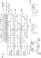
본 발명의 소정의 양태들은 전화기, 모바일 컴퓨팅 디바이스, 어플라이언스, 자동차 일렉트로닉스, 항공전자 시스템들 등과 같은 장치의 서브컴포넌트들을 포함할 수도 있는 전자 디바이스들 간에 전개된 통신 링크들에 적용가능할 수도 있다. 도 1 은 IC 디바이스들 간에 통신 링크를 채용할 수도 있는 장치를 도시한다. 하나의 예에서, 장치 (100) 는 RF 트랜시버를 통해 무선 액세스 네트워크 (RAN), 코어 액세스 네트워크, 인터넷 및/또는 다른 네트워크와 통신하는 무선 통신 디바이스를 포함할 수도 있다. 장치 (100) 는 프로세싱 회로 (102) 에 동작가능하게 커플링된 통신 트랜시버 (106) 를 포함할 수도 있다. 프로세싱 회로 (102) 는 주문형 IC (application-specific IC; ASIC) (108) 와 같은 하나 이상의 IC 디바이스들을 포함할 수도 있다. ASIC (108) 은 하나 이상의 프로세싱 디바이스들, 로직 회로들 등을 포함할 수도 있다. 프로세싱 회로 (102) 는 프로세싱 회로 (102) 에 의해 실행될 수도 있는 명령들 및 데이터를 유지할 수도 있는 메모리 (112) 와 같은 프로세서 판독가능 스토리지를 포함하거나 및/또는 그 프로세서 판독가능 스토리지에 커플링될 수도 있다. 프로세싱 회로 (102) 는 무선 디바이스의 메모리 디바이스 (112) 와 같은 저장 매체들에 상주하는 소프트웨어 모듈들의 실행을 지원하고 가능하게 하는 애플리케이션 프로그래밍 인터페이스 (application programming interface; API) (110) 계층 및 오퍼레이팅 시스템 중 하나 이상에 의해 제어될 수도 있다. 메모리 디바이스 (112) 는 판독 전용 메모리 (ROM) 또는 랜덤 액세스 메모리 (RAM), 전기적으로 소거가능한 프로그래밍가능 ROM (EEPROM), 플래시 카드들, 또는 프로세싱 시스템들 및 컴퓨팅 플랫폼들에서 이용될 수 있는 임의의 메모리 디바이스를 포함할 수도 있다. 프로세싱 회로 (102) 는 장치 (100) 를 구성하고 동작시키는데 이용되는 동작 파라미터들 및 다른 정보를 유지할 수 있는 로컬 데이터베이스 (114) 를 포함하거나 또는 그 로컬 데이터베이스 (114) 에 액세스할 수도 있다. 로컬 데이터베이스 (114) 는 데이터베이스 모듈, 플래시 메모리, 자기 매체들, EEPROM, 광 매체들, 테이프, 소프트 또는 하드 디스크 등 중 하나 이상을 이용하여 구현될 수도 있다. 프로세싱 회로 (102) 는 또한 외부 디바이스들, 예컨대 안테나 (122), 디스플레이 (124), 오퍼레이터 컨트롤들, 예컨대 다른 컴포넌트들 중에서도 버튼 (128) 및 키패드 (126) 에 동작가능하게 커플링될 수도 있다.Certain aspects of the present invention may be applicable to communication links deployed between electronic devices that may include subcomponents of devices such as telephones, mobile computing devices, appliances, automotive electronics, avionics systems, and the like. Figure 1 illustrates an apparatus that may employ a communication link between IC devices. In one example, the
도 2 는 무선 모바일 디바이스, 모바일 전화기, 모바일 컴퓨팅 시스템, 무선 전화기, 노트북 컴퓨터, 태블릿 컴퓨팅 디바이스, 미디어 플레이어, 게이밍 디바이스 등과 같은 장치의 소정의 양태들을 예시하는 블록 개략도 (200) 이다. 장치 (200) 는 통신 링크 (220) 를 통해 데이터 및 제어 정보를 교환하는 복수의 IC 디바이스들 (202 및 230) 을 포함할 수도 있다. 통신 링크 (220) 는, 서로 아주 근접하여 위치되거나 또는 장치 (200) 의 상이한 부분들에 물리적으로 위치되는 IC 디바이스들 (202, 230) 의 쌍을 연결하는데 이용될 수도 있다. 하나의 예에서, 통신 링크 (220) 는 IC 디바이스들 (202 및 230) 을 지니는 칩 캐리어, 기판 또는 회로 판 상에 제공될 수도 있다. 다른 예에서, 제 1 IC 디바이스 (202) 는 플립-폰 (flip-phone) 의 키패드 섹션에 위치될 수도 있는 한편 제 2 IC 디바이스 (230) 는 플립-폰의 디스플레이 섹션에 위치될 수도 있다. 다른 예에서, 통신 링크 (220) 의 일부는 케이블 또는 광 연결을 포함할 수도 있다.2 is a block schematic diagram 200 illustrating certain aspects of a device such as a wireless mobile device, a mobile telephone, a mobile computing system, a wireless telephone, a notebook computer, a tablet computing device, a media player, a gaming device,
통신 링크 (220) 는 다수의 채널들 (222, 224 및 226) 을 포함할 수도 있다. 하나 이상의 채널 (226) 은 양방향성일 수도 있고, 하프-듀플렉스 (half-duplex) 모드 및/또는 풀-듀플렉스 (full-duplex) 모드에서 동작할 수도 있다. 하나 이상의 채널 (222 및 224) 은 단방향성일 수도 있다. 통신 링크 (220) 는 비대칭적이어서, 하나의 방향에서 더 높은 대역폭을 제공할 수도 있다. 본 명세서에서 설명된 하나의 예에서, 제 1 통신 채널 (222) 은 순방향 링크 (222) 라고 지칭될 수도 있는 한편 제 2 통신 채널 (224) 은 역방향 링크 (224) 라고 지칭될 수도 있다. 제 1 IC 디바이스 (202) 가 호스트 시스템 또는 송신기로서 지정될 수도 있는 한편, 제 2 IC 디바이스 (230) 가 클라이언트 시스템 또는 수신기로서 지정될 수도 있는데, 양쪽의 IC 디바이스들 (202 및 230) 이 통신 링크 (222) 상에서 송신 및 수신하도록 구성되더라도 그러하다. 하나의 예에서, 순방향 링크 (222) 는 제 1 IC 디바이스 (202) 로부터의 데이터를 제 2 IC 디바이스 (230) 로 통신할 때 보다 높은 데이터 레이트에서 동작할 수도 있는 한편, 역방향 링크 (224) 는 제 2 IC 디바이스 (230) 로부터의 데이터를 제 1 IC 디바이스 (202) 로 통신할 때 보다 낮은 데이터 레이트에서 동작할 수도 있다.The
IC 디바이스들 (202 및 230) 은 각각 프로세서 또는 다른 프로세싱 및/또는 컴퓨팅 회로 또는 디바이스 (206, 236) 를 포함할 수도 있다. 하나의 예에서, 제 1 IC 디바이스 (202) 는 무선 트랜시버 (204) 및 안테나 (214) 를 통해 무선 통신을 유지하는 것을 포함하는, 장치 (200) 의 코어 기능들을 수행할 수도 있는 한편, 제 2 IC 디바이스 (230) 는 디스플레이 제어기 (232) 를 관리하거나 또는 동작시키는 사용자 인터페이스를 지원할 수도 있고, 카메라 제어기 (234) 를 이용하여 카메라 또는 비디오 입력 디바이스의 동작들을 제어할 수도 있다. IC 디바이스들 (202 및 230) 중 하나 이상에 의해 지원되는 다른 피처들은 키보드, 음성-인식 컴포넌트, 및 다른 입력 또는 출력 디바이스들을 포함할 수도 있다. 디스플레이 제어기 (232) 는 액정 디스플레이 (LCD) 패널, 터치-스크린 디스플레이, 표시자들 등과 같은 디스플레이들을 지원하는 회로들 및 소프트웨어 드라이버들을 포함할 수도 있다. 저장 매체들 (208 및 238) 은 각각의 프로세서들 (206 및 236) 및/또는 IC 디바이스들 (202 및 230) 의 다른 컴포넌트들에 의해 이용되는 명령들 및 데이터를 유지하도록 적응된 일시적 및/또는 비일시적 저장 디바이스들을 포함할 수도 있다. 각각의 프로세서 (206, 236) 와 그의 대응하는 저장 매체들 (208 및 238) 및 다른 모듈들 및 회로들 간의 통신은 하나 이상의 버스 (212 및 242) 에 의해 각각 용이해질 수도 있다.
역방향 링크 (224) 는 순방향 링크 (222) 와 동일한 방식으로 동작될 수도 있고, 순방향 링크 (222) 및 역방향 링크 (224) 는 비슷한 속도들로 또는 상이한 속도들로 송신하는 것이 가능할 수도 있는데, 여기서 속도는 데이터 전송 레이트 및/또는 클록킹 레이트들로서 표현될 수도 있다. 순방향 및 역방향 데이터 레이트들은, 애플리케이션에 따라, 실질적으로 동일할 수도 있거나 또는 몇 자릿수 만큼 상이할 수도 있다. 일부 애플리케이션들에서, 단일의 양방향성 링크 (226) 는 제 1 IC 디바이스 (202) 와 제 2 IC 디바이스 (230) 사이의 통신들을 지원할 수도 있다. 순방향 링크 (222) 및/또는 역방향 링크 (224) 는, 예를 들어, 순방향 및 역방향 링크들 (222 및 224) 이 동일한 물리적 연결들을 공유하고 하프-듀플렉스 방식으로 동작할 때, 양방향성 모드에서 동작하도록 구성가능할 수도 있다. 하나의 예에서, 통신 링크 (220) 는 산업 또는 다른 표준에 따라 제 1 IC 디바이스 (202) 와 제 2 IC 디바이스 (230) 사이에서 제어, 커맨드 및 다른 정보를 통신하도록 동작될 수도 있다.The
산업 표준들은 특수 용도일 수도 있다. 하나의 예에서, MIPI 표준은 모바일 디바이스에서 카메라 또는 디스플레이를 지원하는 IC 디바이스 (230) 와 애플리케이션 프로세서 IC 디바이스 (202) 사이에 동기 인터페이스 명세 (D-PHY) 를 포함하는 물리 계층 인터페이스들을 정의한다. D-PHY 규격은 모바일 디바이스들에 대한 MIPI 규격들을 준수하는 제품들의 동작 특성들을 지배한다. D-PHY 인터페이스는 모바일 디바이스 내의 컴포넌트들 (202 및 230) 사이를 상호연결하는 플렉서블한, 저가의, 고속 직렬 인터페이스를 이용하여 데이터 전송들을 지원할 수도 있다. 이들 인터페이스들은 전자기 간섭 (EMI) 이슈들을 회피하기 위해 슬로우 에지들과 함께 비교적 낮은 비트 레이트들을 제공하는 상보형 금속-산화물-반도체 (CMOS) 병렬 버스들을 포함할 수도 있다.Industry standards may be of special use. In one example, the MIPI standard defines physical layer interfaces that include a Synchronization Interface Specification (D-PHY) between an application
도 2 의 통신 링크 (220) 는 복수의 신호 와이어 (wire) 들 (M 개의 와이어들로서 표시됨) 을 포함하는 유선 버스로서 구현될 수도 있다. M 개의 와이어들은 모바일 디스플레이 디지털 인터페이스 (mobile display digital interface; MDDI) 와 같은 고속 디지털 인터페이스에서 N-위상 (N-phase) 인코딩된 데이터를 반송하도록 구성될 수도 있다. M 개의 와이어들은 하나 이상의 채널들 (222, 224 및 226) 상에서 N-위상 극성 인코딩을 용이하게 할 수도 있다. 물리 계층 드라이버들 (210 및 240) 은 통신 링크 (220) 상의 송신을 위해 N-위상 극성 인코딩된 데이터를 생성하도록 구성 또는 적응될 수도 있다. N-위상 극성 인코딩의 이용은 고속 데이터 전송을 제공하고, 보다 적은 드라이버들이 N-위상 극성 인코딩된 데이터 링크들 (220) 에서 액티브 (active) 하기 때문에 다른 인터페이스들의 전력의 절반 이하를 소비할 수도 있다.The
N-위상 극성 인코딩 디바이스들 (210 및/또는 240) 은 통상적으로 통신 링크 (220) 상에서 천이 당 다수의 비트들을 인코딩할 수 있다. 하나의 예에서, 3-위상 인코딩 및 극성 인코딩의 조합이 프레임 버퍼 없이 제 2 LCD 드라이버 IC 당 와이드 비디오 그래픽스 어레이 (wide video graphics array; WVGA) 80 프레임들을 지원하는데 이용되어, 디스플레이 리프레시를 위해 810 Mbps 로 픽셀 데이터를 전달할 수도 있다. The N -phase
도 3 은 도 2 에 도시된 통신 링크 (220) 의 소정의 양태들을 구현하는데 이용될 수도 있는 M-와이어, N-위상 극성 인코더를 예시하는 개략적 다이어그램 (300) 이다. 도시된 예에서, M-와이어, N-위상 극성 인코더 송신기는 M=3 와이어 및 N=3 위상 시그널링을 이용하여 정보를 송신하도록 구성된다. 3-와이어, 3-위상 인코딩의 예는 오로지 본 발명의 소정의 양태들의 설명들을 단순화하는 목적을 위해서만 선택된다. 3-와이어, 3-위상 인코더들에 대해 개시된 원리들 및 기법들은 M-와이어, N-위상 극성 인코더들의 다른 구성들에 응용될 수 있다.FIG. 3 is a schematic diagram 300 illustrating an M -wire, N -phase polarity encoder that may be used to implement certain aspects of the
M-와이어, N-위상 극성 인코딩 스킴에서의 M 개의 와이어들 각각에 대해 정의된 시그널링 상태들은 포지티브로 구동된 (driven) 상태, 네거티브로 구동된 상태 및 미구동된 (undriven) 상태를 포함할 수도 있다. 3-와이어, 3-위상 극성 인코딩 스킴에서, 포지티브로 구동된 상태 및 네거티브로 구동된 상태는 신호 와이어들 (310a, 310b 및/또는 310c) 중 2 개 사이의 전압 차분 (voltage differential) 을 제공함으로써 및/또는 직렬로 연결된 신호 와이어들 (310a, 310b 및/또는 310c) 중 2 개를 통해 전류를 구동하여 그 전류가 2 개의 신호 와이어들 (310a, 310b 및/또는 310c) 에서 상이한 방향들로 흐르도록 함으로써 획득될 수도 있다. 통상적으로, 미구동된 신호 와이어 (310a, 310b 또는 310c) 를 통한 유의한 전류 흐름이 없다. 3-와이어, 3-위상 극성 인코딩 스킴에 대해 정의된 시그널링 상태들은 3개 전압 또는 전류 상태들 (+1, -1, 및 0) 을 이용하여 표시될 수도 있다.The signaling states defined for each of the M wires in the M -wire, N -phase polarity encoding scheme may include a positively driven state, a negatively driven state, and an undriven state have. In the three-wire, three-phase polarity encoding scheme, the positively driven and negatively driven states provide a voltage differential between two of the
미구동된 상태 (즉, 0 상태) 는, 수동으로 또는 능동으로 "미구동된" 신호 와이어 (310a, 310b 또는 310c) 로 하여금, 구동된 신호 와이어들 (310a, 310b 및/또는 310c) 상에 제공된 포지티브와 네거티브 전압 레벨들 사이에서 실질적으로 중간에 놓인 전압 레벨을 가지게 함으로써 신호 와이어 (310a, 310b 또는 310c) 상에서 획득될 수도 있다. 하나의 예에서, 미구동된 상태는 신호 와이어 (310a, 310b 또는 310c) 의 드라이버의 출력을 하이-임피던스 모드에 놓이게 함으로써 실현될 수도 있다. 3-위상 0 상태, 미구동된 상태, 및 하이-임피던스 상태는 단일의 신호 와이어 (310a, 310b 또는 310c) 의 관점에서 3-위상 시그널링 스킴에서 전기적으로 등가일 수도 있다. 그러나, 신호 와이어들 (310a, 310b 또는 310c) 중 하나만이 심볼에서 미구동된 상태에 있을 수 있다. 이에 따라, 심볼은 3 개의 신호 와이어들 (310a, 310b, 310c) 중 2 개가 하이-임피던스 상태에 있는 경우 에러 심볼인 것으로 고려될 수도 있다. 3 개의 신호 와이어들 (310a, 310b, 310c) 모두가 하이-임피던스 상태에 있는 경우, 통신 링크 (220) 는 인액티브 (inactive) 한 것으로 고려될 수도 있다.The undriven state (i. E., The 0 state) allows either manually or actively "unactuated"
3-와이어, 3-위상 극성 인코더는 커넥터들 (310a, 310b 및 310c) 의 시그널링 상태를 제어하기 위해 드라이버들 (308) 을 채용할 수도 있다. 드라이버들 (308) 은 유닛-레벨 전류-모드 또는 전압-모드 드라이버들로서 구현될 수도 있다. 하나의 예에서, 각각의 드라이버 (308) 는 대응하는 커넥터들 (310a, 310b 또는 310c) 의 출력 상태를 결정하는 2 개 이상의 신호들의 세트들 (316a, 316b 및 316c) 을 수신할 수도 있다. 신호들의 세트들 (316a, 316b 및 316c) 각각이 한 쌍의 신호들을 포함할 때, 대응하는 커넥터들 (310a, 310b 및 310c) 에 대해 4 개의 상태들이 정의될 수도 있다. 신호들의 세트들 (316a, 316b 및 316c) 각각이 3 개의 신호들을 포함할 때, 대응하는 커넥터들 (310a, 310b 및 310c) 에 대해 8 개의 상태들이 정의될 수도 있다.A three-wire, three-phase polarity encoder may employ
M-와이어, N-위상 극성 인코딩 스킴에서의 각각의 송신된 심볼 간격에 대해, 적어도 하나의 신호 와이어 (310a, 310b 또는 310c) 는 미구동된 (0) 전압 또는 전류 상태에 있는 한편, 포지티브로 구동된 (+1 전압 또는 전류 상태) 신호 와이어들 (310a, 310b 또는 310c) 의 수는 네거티브로 구동된 (-1 전압 또는 전류 상태) 신호 와이어들 (310a, 310b 또는 310c) 의 수와 동일하여, 수신기로 흐르는 전류의 합이 항상 제로가 되도록 한다. 각각의 심볼에 대해, 적어도 하나의 신호 와이어 (310a, 310b 또는 310c) 의 상태는 선행하는 송신 간격에서 송신된 심볼로부터 변화된다. For each transmitted symbol interval in the M -wire, N -phase polarity encoding scheme, at least one
동작시, 맵퍼 (mapper; 302) 는 16 비트 데이터 (310) 를 수신하여 이 16 비트 데이터를 7 개의 심볼들 (312) 에 맵핑시킬 수도 있다. 3-와이어 예에서, 7 개의 심볼들 각각은 하나의 심볼 간격에 대한 신호 와이어들 (310a, 310b 및 310c) 의 상태들을 정의한다. 7 개의 심볼들 (312) 은 각각의 와이어 (310a, 310b 및 310c) 에 대한 상태들 (314) 의 타이밍된 시퀀스를 제공하는 병렬-직렬 컨버터 (parallel-to-serial converter; 304) 들을 이용하여 직렬화될 수도 있다. 상태들 (314) 의 시퀀스는 통상적으로 송신 클록을 이용하여 타이밍된다. M-와이어 위상 인코더 (306) 는 한번에 하나의 심볼씩 맵퍼에 의해 생성된 7 개의 심볼들 (314) 의 시퀀스를 수신하고 각각의 심볼 간격에 대한 각각의 신호 와이어 (310a, 310b 및 310c) 의 상태를 컴퓨팅한다. 3-와이어 인코더 (306) 는 신호 와이어들 (310a, 310b 및 310c) 의 이전 상태들 및 현재 입력 심볼 (314) 에 기초하여 신호 와이어들 (310a, 310b 및 310c) 의 상태들을 선택한다.In operation, the
M-와이어, N-위상 인코딩의 이용은 복수의 심볼들에서 다수의 비트들이 인코딩되는 것을 가능하게 하는데 여기서 심볼 당 비트들은 정수가 아니다. 3-와이어 통신 링크의 단순한 예에서, 동시에 구동될 수도 있는 2 개의 와이어들의 3 개의 이용가능한 조합들, 및 구동되는 와이어들의 쌍에 대한 극성의 2 개의 가능한 조합들이 존재하여, 6 개의 가능한 상태들이 산출된다. 현재 상태로부터 각각의 천이가 발생하므로, 6 개의 상태들 중 5 개가 매 천이마다 이용가능하다. 적어도 하나의 와이어의 상태는 각각의 천이에서 변화하도록 요구된다. 5 개의 상태들의 경우, log2(5)![]()
![]()
도 4 는 원형 상태 다이어그램 (450) 에 기초하는 3-위상 변조 데이터-인코딩 스킴을 이용하여 인코딩된 신호들에 대한 타이밍 차트 (400) 의 예를 포함한다. 정보는, 예를 들어, 와이어 또는 커넥터가 상태 다이어그램 (450) 에 의해 정의된 3 개의 위상 상태들 S 1, S 2 및 S 3 중 하나에 있는 시그널링 상태들의 시퀀스에서 인코딩될 수도 있다. 각각의 상태는 120°위상 시프트만큼 다른 상태들로부터 분리될 수도 있다. 하나의 예에서, 데이터는 와이어 또는 커넥터에 대한 위상 상태들의 회전의 방향으로 인코딩될 수도 있다. 신호에서의 위상 상태들은 시계 방향 (452 및 452') 또는 반시계 방향 (454 및 454') 으로 회전할 수도 있다. 예를 들어 시계 방향 (452 및 454') 에서, 위상 상태들은 S 1 로부터 S 2 로, S 2 로부터 S 3 으로 그리고 S 3 으로부터 S 1 로의 천이들 중 하나 이상을 포함하는 시퀀스로 나아갈 수도 있다. 반시계 방향 (454 및 454') 에서, 위상 상태들은 S 1 로부터 S 3 으로, S 3 으로부터 S 2 로 그리고 S 2 로부터 S 1 로의 천이들 중 하나 이상을 포함하는 시퀀스로 나아갈 수도 있다. 3 개의 와이어들 (310a, 310b 및 310c) 은 동일한 신호의 상이한 버전들을 반송하는데, 여기서 그 버전들은 서로에 대해 120°만큼 위상 시프트된다. 각각의 시그널링 상태는 와이어 또는 커넥터에 대한 상이한 전압 레벨 및/또는 와이어 또는 커넥터를 통한 전류 흐름의 방향으로서 표현될 수도 있다. 3-와이어 시스템에서의 시그널링 상태들의 시퀀스 각각 동안에, 각각의 와이어 (310a, 310b 및 310c) 는 다른 와이어들과는 상이한 시그널링 상태들에 있다. 3 개를 초과하는 와이어들 (310a, 310b 및 310c) 이 3-위상 인코딩 시스템에서 이용될 때, 2 개 이상의 와이어들 (310a, 310b 및/또는 310c) 은 각각의 시그널링 간격에서 동일한 시그널링 상태에 있을 수 있지만, 각각의 상태는 매 시그널링 간격마다 적어도 하나의 와이어 (310a, 310b 및/또는 310c) 에 대해 존재한다.FIG. 4 includes an example of a
정보는 각각의 위상 천이 (410) 에서의 회전의 방향으로 인코딩될 수도 있고, 3-위상 신호는 각각의 시그널링 상태에 대한 방향을 변화시킬 수도 있다. 회전의 방향은, 미구동된 와이어 (310a, 310b 및/또는 310c) 가, 회전의 방향에 상관없이, 회전하는 3-위상 신호에서 매 시그널링 상태마다 변화하기 때문에, 어느 와이어들 (310a, 310b 및/또는 310c) 이 위상 천이의 전과 후에 '0' 상태에 있는지를 고려함으로써 결정될 수도 있다.The information may be encoded in the direction of rotation at each
인코딩 스킴은 또한 능동으로 구동되는 도체들 (310a, 310b 및 310c) 중 2 개의 도체의 극성 (408) 에서의 정보를 인코딩할 수도 있다. 3-와이어 구현에서 임의의 시간에, 도체들 (310a, 310b, 310c) 중 정확히 2 개는 반대 방향의 전류들로 및/또는 전압 차분으로 구동된다. 단순한 구현에서, 데이터 (412) 는 2 비트 값들 (412) 을 이용하여 인코딩될 수도 있는데, 여기서 하나의 비트는 위상 천이들 (410) 의 방향으로 인코딩되고 두 번째 비트는 현재 상태에 대한 극성 (408) 으로 인코딩된다.The encoding scheme may also encode information at the polarity 408 of the two conductors of the actively driven
타이밍 차트 (400) 는 위상 회전 방향과 극성 양쪽 모두를 이용하는 데이터 인코딩을 예시한다. 곡선들 (402, 404 및 406) 은, 다수의 위상 상태들에 대한, 3 개의 와이어들 (310a, 310b 및 310c) 상에서 반송된 신호들 각각에 관한 것이다. 초기에는, 위상 천이들 (410) 은 시계 방향으로 있고, 최상위 비트는, 그 최상위 비트의 바이너리 '0' 에 의해 표현된 바와 같이, 위상 천이들 (410) 의 회전이 시간 414 에서 반시계 방향으로 스위칭할 때까지 바이너리 '1' 로 설정된다. 최하위 비트는 각각의 상태에서 신호의 극성 (408) 을 반영한다.The
본 명세서에 개시된 소정의 양태들에 따르면, 데이터의 1 비트는 3-와이어, 3-위상 인코딩 시스템에서의 회전, 또는 위상 변화로 인코딩될 수도 있고, 부가적인 비트는 2 개의 구동된 와이어들의 극성으로 인코딩될 수도 있다. 부가적인 정보는 현재 상태로부터 가능한 상태들 중 임의의 상태로의 천이를 가능하게 함으로써 3-와이어, 3-위상 인코딩 시스템의 각각의 천이에서 인코딩될 수도 있다. 3 개의 회전 위상들 및 각각의 위상에 대한 2 개의 극성들을 고려하면, 6 개의 상태들이 3-와이어, 3-위상 인코딩 시스템에서 이용가능하다. 이에 따라, 5 개의 상태들이 임의의 현재 상태로부터 이용가능하다. 이에 따라, 심볼 (천이) 당 인코딩된 log2(5)![]()
![]()
N-위상 데이터 전송은 버스와 같은, 통신 매체에 제공된 3 개를 초과하는 와이어들을 이용할 수도 있다. 동시에 구동될 수 있는 부가적인 신호 와이어들의 이용은 상태들과 극성들의 더 많은 조합들을 제공하고, 데이터의 더 많은 비트들이 상태들 간의 각각의 천이에서 인코딩되게 한다. 이것은, 증가된 대역폭을 제공하면서, 데이터 비트들을 송신하기 위해 다수의 차분 쌍들을 이용하는 접근법들에 비해 시스템의 스루풋을 현저히 개선시키고 전력 소비를 감소시킬 수 있다.N-phase data transmission may utilize more than three wires provided in the communication medium, such as a bus. The use of additional signal wires that can be driven simultaneously provides more combinations of states and polarities and allows more bits of data to be encoded at each transition between states. This can significantly improve system throughput and reduce power consumption compared to approaches using multiple differential pairs to transmit data bits while providing increased bandwidth.
하나의 예에서, 인코더는 각각의 상태에 대해 구동된 와이어들의 2 개의 쌍들을 가진 6 개의 와이어들을 이용하여 심볼들을 송신할 수도 있다. 6 개의 와이어들은 A 내지 F 로 라벨링될 수도 있어서, 하나의 상태에서, 와이어들 A 및 F 는 포지티브 구동되고, 와이어들 B 및 E 는 네거티브 구동되며, C 및 D 는 미구동 (전류를 나르지 않음) 된다. 6 개의 와이어들에 대해, 다음과 같이 능동으로 구동된 와이어들의:In one example, the encoder may transmit symbols using six wires with two pairs of wires driven for each state. The six wires may be labeled A to F so that in one state wires A and F are positively driven and wires B and E are negatively driven and C and D are not driven ) do. For six wires, one of the following actively driven wires:

개의 가능한 조합들이 존재할 수도 있고, 여기서 각각의 위상 상태에 대한 극성의:There may be four possible combinations of polarity for each phase state:

개의 상이한 조합들이 존재한다.There are different combinations.
능동으로 구동된 와이어들의 15 개의 상이한 조합들은 다음을 포함할 수도 있다:The fifteen different combinations of actively driven wires may include the following:

구동된 4 개의 와이어들 중, 2 개의 와이어들의 가능한 조합들이 포지티브 구동된다 (그리고 나머지 2 개는 네거티브이어야 한다). 극성의 조합들은 다음을 포함할 수도 있다: Of the four wires driven, the possible combinations of the two wires are positively driven (and the other two must be negative). The combinations of polarities may include:
![]()
![]()
이에 따라, 상이한 상태들의 총 수는 15 × 6 = 90 으로서 계산될 수도 있다. 심볼들 간의 천이를 보장하기 위해, 89 개의 상태들이 임의의 현재 상태로부터 이용가능하며, 각각의 심볼에서 인코딩될 수도 있는 비트들의 수는 심볼 당 log2(89)![]()
![]()
임의의 사이즈의 버스에 대해 구동될 수 있는 와이어들의 조합들의 수에 대한 일반식은, 버스에서의 와이어들의 수 및 동시에 구동된 와이어들의 수의 함수로서, 다음과 같다:A general expression for the number of combinations of wires that can be driven for a bus of arbitrary size is a function of the number of wires in the bus and the number of simultaneously driven wires as follows:

구동되는 와이어들에 대한 극성의 조합들의 수에 대한 식은 다음과 같다:The formula for the number of combinations of polarities for the driven wires is:

심볼 당 비트들의 수는 다음과 같다:The number of bits per symbol is:

도 5 는 3-와이어, 3-위상 디코더에서의 수신기의 소정의 양태들을 예시하는 블록 개략도 (500) 를 포함한다. 차동 수신기들 (502a, 502b 및 502c) 의 세트는 3 개의 와이어들 (510a, 510b 및 510c) 각각을 3 개의 와이어들 (510a, 510b 및 510c) 중 다른 것과 비교하도록 구성된다. 도시된 예에서, 차동 수신기 (502a) 는 와이어들 (510a 및 510b) 의 상태들을 비교하고 A-B 차이 신호 (504a) 를 출력하고, 차동 수신기 (502b) 는 와이어들 (510b 및 510c) 의 상태들을 비교하고 B-C 차이 신호 (504b) 를 출력하며, 차동 수신기 (502c) 는 와이어들 (510a 및 510c) 의 상태들을 비교하고 C-A 차이 신호 (504c) 를 출력한다. 이에 따라, 위상 변화 검출 회로 (506) 는 차동 수신기들 (502a, 502b 및 502c) 중 적어도 하나의 차동 수신기의 출력 (504a, 504b 및/또는 504c) 이 각각의 위상 간격의 끝에서 변화하기 때문에 위상 변화의 발생을 검출하도록 구성될 수 있다.FIG. 5 includes a block schematic 500 illustrating certain aspects of a receiver in a three-wire, three-phase decoder. The set of
소정의 위상 천이들은 단일의 차동 수신기 (502a, 502b 또는 502c) 에 의해 검출가능할 수도 있는 한편, 다른 위상 천이들은 차동 수신기들 (502a, 502b 및 502c) 중 2 개 이상에 의해 검출될 수도 있다. 하나의 예에서, 상태들, 또는 2 개의 와이어들의 상대적 상태들은 천이 후에 변화되지 않을 수도 있고, 대응하는 차동 수신기 (502a, 502b 또는 502c) 의 출력이 또한 위상 천이 후에 변화되지 않을 수도 있다. 다른 예에서, 한 쌍의 와이어들 (510a, 510b 및/또는 510c) 에서의 양쪽의 와이어들은 제 1 시간 간격에서 동일한 상태에 있을 수도 있고 양쪽의 와이어들은 제 2 시간 간격에서 동일한 제 2 상태에 있을 수도 있고, 와이어들의 쌍을 비교하는 차동 수신기 (502a, 502b 또는 502c) 는 위상 천이 후에 변화되지 않을 수도 있다. 이에 따라, 클록 생성 회로는 수신 (Rx) 위상 천이가 발생한 때를 결정하기 위해 모든 차동 수신기들 (502a, 502b 및 502c) 의 출력들을 모니터링하는 위상 변화 검출 회로들 및 로직 (506) 을 포함할 수도 있다. 클록 생성 회로는 신호들 (508a, 508b 및 508c) 로서 각각 출력되는 검출된 위상 천이들 Rx_AB, Rx_BC 및/또는 Rx_CA 에 기초하여 수신 클록 (512) 을 생성할 수도 있다.Certain phase transitions may be detectable by a single
위상 상태들의 변화들은 와이어들 (510a, 510b 및/또는 510c) 의 상이한 조합들에 대한 상이한 시간들에서 검출될 수도 있다. 위상 상태 변화들의 검출의 타이밍은 발생한 위상 상태 변화의 타입에 따라 가변할 수도 있다. 이 가변성의 결과는 도 5 의 단순화된 타이밍 차트 (520) 에 예시된다. 위상 변화 검출 회로들 (506) 및/또는 차동 수신기들 (502a, 502b 및 502c) 의 출력들을 표현하는 마커들 (522, 524 및 526) 은 단지 예시의 명료함을 위해 상이한 높이들을 할당받는다. 마커들 (522, 524 및 526) 의 상대적 높이들은 클록 생성 또는 데이터 디코딩을 위해 이용된 전압 또는 전류 레벨들, 극성 또는 가중 값들에 대해 어떤 특정 관계도 갖지 않는다. 타이밍 차트 (520) 는 3 개의 와이어들 (510a, 510b 및 510c) 상의 위상 및 극성에 있어서의 송신된 심볼들과 연관된 천이들의 타이밍의 영향을 예시한다. 타이밍 차트 (520) 에서, 일부 심볼들 간의 천이들은 심볼들이 신뢰성있게 캡처될 수도 있는 가변 캡처 윈도우들 (530a, 530b, 530c, 530d, 530e, 530f 및/또는 530g) (통칭하여 심볼 캡처 윈도우들 (530)) 을 발생시킬 수도 있다. 검출된 상태 변화들의 수 및 그들의 상대적 타이밍은 클록 신호 (512) 상에 지터를 발생시킬 수 있다.Changes in phase states may be detected at different times for different combinations of
3-와이어, 3-위상 통신 링크를 시뮬레이션할 때, 와이어들의 소정의 아날로그 특성들은 심볼 윈도우들 (530) 에서의 가변성, 및 이러한 가변성으로부터 발생할 수도 있는 지터를 고려하도록 모델링될 수도 있다. 심볼 윈도우들 (530) 의 사이즈들에서의 가변성 및 지터는, 도 6 에 도시된 단순 예 (600) 에 예시한 바와 같이, 와이어들 (510a, 510b 및 510c) 의 아날로그 전기적 특성들에 의해 부분적으로 야기될 수도 있다. 더 구체적으로는, 상승 및 하강 시간들에 영향을 미치는 와이어들 (510a, 510b 및 510c) 의 아날로그 전기 특성들은 저항, 커패시턴스, 인덕턴스, 라인 드라이버들에 의해 제공된 전압들 및 전류들, 라인 수신 회로들에서 설정된 임계치, 및 다른 팩터들을 포함할 수도 있다. 심볼 윈도우들 (530) 의 사이즈들에서의 가변성은 제조 프로세스 허용오차들, 전압 및 전류 소스들의 변동들 및 안정성 및 오퍼레이팅 온도에 의해 야기되는 검출 회로들에서의 가변성 및/또는 신호 천이 시간들에서의 가변성에 의해 영향을 받을 수도 있다.When simulating a three-wire, three-phase communication link, certain analog characteristics of the wires may be modeled to account for the variability in the
신호 천이 시간들에서의 큰 가변성은 3-위상 시그널링에서의 상이한 전압 또는 전류 레벨들의 존재에 기인할 수 있다. 단순화된 "전압-레벨" 예는 단일의 와이어 (510a, 510b 또는 510c) 에서의 천이 시간들을 예시하는 도 6 에 도시된다. 제 1 심볼 (Sym n ) 간격 (602) 은 시간 622 에서 종료할 수도 있고, 제 2 심볼 (Sym n+1 ) 간격은 시간 624 에서 종료할 수도 있으며 제 3 심볼 (Sym n+2 ) 간격 (606) 은 시간 626 에서 종료할 수도 있고, 그 때 제 4 심볼 (Sym n+3 ) 간격 (608) 이 시작된다. 제 1 심볼 (602) 에 의해 결정된 상태로부터 제 2 심볼 (604) 에 대응하는 상태로의 천이는 와이어 (510a, 510b 또는 510c) 에서의 전압이 임계 전압 (618 및/또는 620) 에 도달하는데 걸리는 시간에 기인하는 딜레이 (612) 후에 검출될 수도 있다. 임계 전압들은 와이어 (510a, 510b 또는 510c) 의 상태를 결정하는데 이용될 수도 있다. 제 2 심볼 (604) 에 의해 결정된 상태로부터 제 3 심볼 (606) 에 대한 상태로의 천이는 와이어 (510a, 510b 또는 510c) 에서의 전압이 임계 전압들 (618 및/또는 620) 중 하나에 도달하는데 걸리는 시간에 기인하는 딜레이 (614) 후에 검출될 수도 있다. 제 3 심볼 (606) 에 의해 결정된 상태로부터 제 4 심볼 (608) 에 대한 상태로의 천이는 와이어 (510a, 510b 또는 510c) 에서의 전압이 임계 전압 (618 및/또는 620) 에 도달하는데 걸리는 시간에 기인하는 딜레이 (616) 후에 검출될 수도 있다.The large variability in signal transition times may be due to the presence of different voltage or current levels in 3-phase signaling. The simplified "voltage-level" example is shown in Fig. 6 illustrating transition times in a
가변 딜레이들 (612, 614, 616) 은 상태들 사이의 전압 차분 및 예를 들어 풀-업 또는 풀-다운 저항기에 의해 신호가 상태를 향해 구동되는지 또는 상태를 향해 풀링되는지 여부에 기인할 수도 있다.The
도 7 은 3-와이어, 3-위상 통신 링크의 하나의 예에서 6 개의 상태들 및 30 개의 가능한 상태 천이들을 예시하는 상태 다이어그램 (700) 이다. 상태 다이어그램 (700) 에서의 가능한 상태들 (702, 704, 706, 712, 714 및 716) 은 도 4 의 다이어그램 (450) 에 도시된 상태들을 포함하고 그 상태들에 대해 확장된다. 예시적인 상태 엘리먼트 (720) 에 도시한 바와 같이, 상태 다이어그램 (700) 에서의 각각의 상태 (702, 704, 706, 712, 714 및 716) 는 (각각 와이어들 (610a, 610b 및 610c) 상에 송신된) 신호들 (A, B 및 C) 의 전압 상태를 나타내는 필드 (722), 차동 수신기들 (502a, 502b, 502c) (도 5 참조) 각각에 의한 와이어 전압들의 감산의 결과를 나타내는 필드 (724) 및 회전의 방향을 나타내는 필드 (726) 를 포함한다. 예를 들어, 상태 (702) (+x) 에서 와이어 A=+1, 와이어 B=-1 및 와이어 C=0 이며, 이는 차동 수신기 (502a) (A-B)=+2, 차동 수신기 (502b) (B-C)=-1 및 차동 수신기 (502c) (C-A)=+1 의 출력을 산출한다. 정의된 상태들 {+1, 0, -1} 은 하나의 예에서 전압 세트 {+V, +V/2, 0} 에 의해, 다른 예에서 전압 세트 {+V, 0, -V} 에 의해, 또는 일부 다른 표현에 의해 510a, 510b 및 510c 에 대해 표현될 수도 있다. 상태 다이어그램에 의해 예시된 바와 같이, 위상 변화 검출 회로 (506) 에 의해 취해진 천이 판정들은 차동 수신기들 (502a, 502b 및 502c) 에 의한 감산에 의해 생성된 5 개의 가능한 레벨들에 기초하며, 이 5 개의 가능한 레벨들은 -2, -1, 0, +1 및 +2 전압 상태들을 포함한다.FIG. 7 is a state diagram 700 illustrating six states and thirty possible state transitions in one example of a three-wire, three-phase communication link.
테이블 1 은 3-와이어 3-위상 인코딩 스킴에 대한 시그널링 상태들을 예시하는데, 여기서 와이어들 (A, B, C) (510a, 510b 및 510c) 은 3 개의 전압 레벨들 {+V, +V/2, 0} 을 스위칭할 수 있다. 차동 수신기들 (502a, 502b, 502c) 각각의 차이 출력들 (504a, 504b 또는 504c) 은 한 쌍의 와이어들 (510a, 510b 및 510c) 의 입력 전압들에서의 차이를 표현한다.Table 1 illustrates the signaling states for a three-wire three-phase encoding scheme where wires A, B,

테이블 1Table 1
도 8 은 테이블 1 의 인코딩/디코딩 스킴을 그래픽으로 도시한다. 위상 변화 검출 회로는 차이 출력 (504a, 504b 또는 504c) 이 포지티브 전압을 갖는 경우에는 로직 '1' 값을 그리고 차이 출력 (504a, 504b 또는 504c) 이 네거티브 전압을 가질 때에는 로직 '0' 값을 갖는 바이너리 신호를 생성하도록 차이 출력들 (504a, 504b 및 504c) 을 프로세싱할 수도 있다.Figure 8 graphically illustrates the encoding / decoding scheme of Table 1; The phase change detection circuit may have a logic '1' value when the
도 8 은 제 1 상태로부터 제 2 상태로의 천이들의 단순화된 예들을 표현하는 타이밍 차트들 (800) 을 제공하고, 신호 와이어들 (504a, 504b 및 504c) 의 아날로그 특성들에 기인하는 타이밍 가변성을 예시한다. 타이밍 차트 (800) 는 3-와이어, 3-위상 통신 링크의 예와 관련된 것으로, 트리오의 와이어들의 3 개의 신호들 사이의 상승 및 하강 시간에서의 약간의 차이들로 인해 그리고 수신된 신호 쌍들 (예를 들어, A-B, B-C, 및 C-A) 의 조합들 사이의 신호 전파 시간들에서의 약간의 차이들로 인해 다수의 수신기 출력 천이들이 각각의 UI 경계에서 발생할 수도 있다. 이 설명의 목적들을 위해, 도 8 에 도시된 신호들은 어떤 위상 지터 또는 ISI 도 갖지 않는다고 가정한다. 와이어의 초기 상태는, 와이어를 +V/2 볼트 레벨로 수동으로 풀링되게 하거나 또는 플로팅하게 함으로써 +V/2 볼트 상태가 획득되는 경우, 다른 구동된 상태 또는 미구동된 상태로의 가능한 천이들을 갖는, 구동된 상태 (0 볼트들 또는 +V 볼트들) 일 수도 있다. 일부 경우들에서, 모든 3 개의 상태들은 구동된 상태들일 수도 있다. 와이어의 초기 상태는, 구동된 상태로의 가능한 천이들을 갖는, 미구동된 상태일 수도 있다.FIG. 8 provides timing charts 800 that illustrate simplified examples of transitions from a first state to a second state and provides timing variations due to analog characteristics of the
타이밍 차트들 (802, 812 및 822) 은 신호 그래프들 (850) 의 세트에 도시된 신호 천이들 전과 후에 차동 수신기들 (502a, 502b 및 502c) 에서 측정가능한 신호 와이어들 (510a, 510b 및 510c) (각각, 신호들 A, B 및 C) 간의 차이들을 예시한다. 도 8 에 도시된 예들에서, -1 상태는 0 볼트들의 전압 레벨에 의해 표현되고, +1 상태는 포지티브 전압 (+V 볼트들) 에 의해 표현되며, 중간 상태는 +V/2 볼트들에서 정의된다. 많은 경우들에서, 차동 수신기들 (502a, 502b 및 502c) 의 세트는 2 개의 신호 와이어들 (510a, 510b 및 510c) 에 대한 상이한 조합들을 비교함으로써 천이들을 캡처하도록 구성될 수도 있다. 하나의 예에서, 이들 차동 수신기들 (502a, 502b 및 502c) 은 이들의 각각의 입력 전압들의 (예를 들어 감산에 의한) 차이를 결정함으로써 출력들을 생성하도록 구성될 수도 있다. 클록은 차동 수신기들 (502a, 502b 및 502c) 중 하나 이상의 차동 수신기의 출력들의 제로-크로싱들에 기초하여 생성될 수도 있다. +1 상태를 표현하는 전압과 -1 상태를 표현하는 전압 사이의 전압 범위 내의 중간점에서의 전압에 의해 표현되는 0 상태를 통해 신호가 천이할 때 제로-크로싱이 발생할 수도 있다. 하나의 예에서, -1 상태가 네거티브 전압 (-V) 에 의해 표현되고 +1 상태가 포지티브 전압 (+V) 에 의해 표현될 때 제로-크로싱은 0 볼트들에서 발생한다.Timing charts 802,812 and 822 illustrate
타이밍 차트들 (802 및 852) 은 신호 A 가 +1 상태로부터 -1 상태로 천이하고, 신호 B 가 -1 상태로부터 +1 상태로 천이하며 신호 C 가 0 상태에 남아있는 심볼 (+x) (702) 로부터 심볼 (-x) (712) 로의 천이 (도 7 참조) 와 관련된다. 이에 따라, 차동 수신기 (502a) 는 AB 천이 (806) 전에 +2 차이 및 AB 천이 (806) 후에 -2 차이를 측정할 수도 있고, 차동 수신기들 (502b 및 502c) 은 각각 BC 및 CA 천이들 (804) 전에 -1 차이 및 BC 및 CA 천이들 (804) 후에 +1 차이를 측정할 수도 있다. 이 예에서, BC 및 CA 천이들 (804 및 806) 양쪽은 제로-크로싱들을 갖는다. 제로-크로싱들은 양쪽 천이들이 구동된 상태들을 향하기 때문에 시간적으로 아주 근접하게 (810) 발생할 수도 있다.Timing charts 802 and 852 illustrate that the signal A transitions from the +1 state to the -1 state and the signal B transitions from the -1 state to the +1 state and the signal C remains at the 0 state 702) to the symbol (-x) 712 (see FIG. 7). Accordingly, the
타이밍 차트들 (812 및 854) 은 신호 A 가 +1 상태로부터 0 상태로 천이하고, 신호 B 가 -1 상태로부터 +1 상태로 천이하며 신호 C 가 0 상태로부터 -1 상태로 천이하는 심볼 (+x) (702) 로부터 심볼 (+y) (704) 로의 천이와 관련된다. 이에 따라, 차동 수신기 (502a) 는 AB 천이 (816) 전에 +2 차이 및 AB 천이 (816) 후에 -1 차이를 측정할 수도 있고, 차동 수신기 (502b) 는 BC 천이 (814) 전에 -1 차이 및 BC 천이 (814) 후에 +2 차이를 측정할 수도 있으며, 차동 수신기 (502c) 는 CA "비-천이" (818) 를 통해 -1 차이에 남아있을 수도 있다. 이 예에서, BC 및 AB 천이들 (814 및 816) 양쪽은 제로-크로싱들을 갖는다. 이들 제로-크로싱들은 상당한 시간 간격 (820) 에 의해 분리될 수도 있다. 하나의 예에서, BC 천이 (814) 가 최종의 구동된 상태를 갖는 2 개의 신호들을 수반하지만 AB 천이 (816) 는 최종의 미구동된 상태를 갖는 하나의 신호와 관련되기 때문에 차이가 발생할 수도 있다.Timing charts 812 and 854 show that the signal A transitions from the +1 state to the 0 state and the signal B transitions from the -1 state to the +1 state and the signal C transitions from the 0 state to the -1 state, x) 702 to a symbol (+ y) 704. [ Accordingly,
타이밍 차트들 (822 및 856) 은 신호 A 가 +1 상태로부터 -1 상태로 천이하고, 신호 B 가 -1 상태로부터 0 상태로 천이하며 신호 C 가 0 상태로부터 +1 상태로 천이하는 심볼 (+x) (702) 로부터 심볼 (+z) (706) 로의 천이와 관련된다. 이에 따라, 차동 수신기 (502a) 는 AB 천이 (826) 전에 +2 차이 및 AB 천이 (826) 후에 -1 차이를 측정할 수도 있고, 차동 수신기 (602b) 는 BC 비-천이 (828) 전과 후에 -1 차이를 측정할 수도 있으며, 차동 수신기 (502c) 는 CA 천이 (824) 전에 -1 차이 및 CA 천이 (824) 후에 +2 차이를 측정할 수도 있다. 이 예에서, CA 및 AB 천이들 (824 및 826) 양쪽은 제로-크로싱들을 갖는다. 이들 제로-크로싱들은 상당한 시간 기간 (period of time; 830) 에 의해 분리될 수도 있다. 하나의 예에서, 차이는 CA 천이 (824) 가 양쪽이 최종의 구동된 상태를 갖는 신호들 (A 및 C) 을 수반하는 한편 AB 천이 (826) 가 최종의 미구동된 상태를 갖는 하나의 신호 (B 신호) 를 수반하는 것에 기인할 수도 있다.Timing charts 822 and 856 show that the signal A transitions from the +1 state to the -1 state and the signal B transitions from the -1 state to the 0 state and the signal C transitions from the 0 state to the +1 state, x) 702 to the symbol (+ z) 706. Accordingly,
제로-크로싱들 간의 시간 간격들 (810, 820 및 830) 은 상태들의 상이한 조합들 간의 천이 시간들의 차이들로부터 발생할 수도 있다. 예를 들어, 구동된 상태로의 천이들에 대한 천이 시간들은 미구동된 상태로의 천이들보다 더 짧다. 상승 시간들의 증가된 또는 감소된 차이들을 생성하는 다른 회로 구현들이 채용될 수도 있다. 예를 들어, 차동 수신기들 (502a, 502b 및 502c) 의 입력들에서의 신호들의 상대적 시간 관계는 제로 상태가 미구동된 레벨보다는 구동된 레벨일 때, 또는 미구동된 신호 와이어가 풀-업 및/또는 풀-다운 저항기들에 의해 종단되는 곳에서 영향을 받을 수도 있다. 따라서, 상이한 타이밍 관계들은 수신기 입력들에서 수신된 신호들에 대해 예상될 수 있다.The
도 8 에 예시된 예들은 +x 로부터 -x 로, +x 로부터 +y 로 및 +x 로부터 +z 로의 3 개의 상태 천이들에 대한 천이들의 정렬을 설명하고, 타이밍 차트들 (852, 854 및 856) 에 도시된 바와 같이, 제로-크로싱들이 신호 와이어들 (510a, 510b 및 510c) 중 적어도 2 개 상에서 발생한다. 이들 3 개의 상태 천이들에서 발생하는 조건들은 도 7 에 도시된 30 개의 가능한 상태 천이들 중 18 개에 존재할 수도 있다.The examples illustrated in FIG. 8 illustrate the alignment of transitions for three state transitions from + x to -x, from + x to + y, and from + x to + z, and timing
본 명세서에서 설명된 소정의 양태들에 따르면, 신호들 및 통신 채널에서 그 신호들을 반송하는 와이어들의 특성들은 시뮬레이션 목적들을 위해 모델링될 수도 있다. 본 명세서에서 설명된 기법들 및 방법들은 3-위상 통신 링크의 동작에 영향을 미칠 수도 있는 와이어들의 소정의 아날로그 특성들을 모델링하는데 이용될 수도 있다. 종래의 시뮬레이터들은 특정 신호들 또는 신호 콘텐츠를 모델링하는 것으로 제한되고 링크의 재구성을 수용할 수 없다. 예를 들어, 종래의 시스템들은 상이한 전력 버짓들을 수용하기 위해 3-위상 시그널링과 바이너리 싱글-엔드형 (single-ended) 또는 차분 시그널링 사이에서 재구성될 수 있는 통신 링크들을 쉽게 시뮬레이션할 수 없다.According to certain aspects described herein, the characteristics of the signals and the wires carrying them in a communication channel may be modeled for simulation purposes. The techniques and methods described herein may be used to model certain analog characteristics of the wires that may affect the operation of a three-phase communication link. Conventional simulators are limited to modeling specific signals or signal content and can not accommodate link reconfiguration. For example, conventional systems can not easily simulate communication links that can be reconfigured between three-phase signaling and binary single-ended or differential signaling to accommodate different power budgets.
본 명세서에서 설명된 소정의 양태들에 따르면, 통신 링크에서의 커넥터는 아날로그 특성들의 실수 모델링에 대한 의존 없이 모델링될 수 있다. 커넥터를 통해 송신된 신호는 커넥터 상에 송신된 신호의 공칭 "액티브/비-액티브" 조건을 나타내기 위해 제 1 바이너리를 비트를 이용하여 표현될 수도 있다. 따라서, 바이너리 신호에 대해, 제 1 바이너리 비트는 로직 '1' 및 로직 '0' 상태들에 직접적으로 맵핑될 수도 있다. 2 개를 초과하는 상태들이 신호에 대해 정의될 때, 커넥터 상의 로직 '1' 및 로직 '0' 상태들을 표현하는 상이한 전압 진폭들을 나타내는 가상 디지털 신호를 제공하기 위해 부가적인 비트들이 이용될 수도 있다. 3-위상 신호의 예에서, 도 8 의 신호 그래프들 (850) 에 그리고 테이블 1 에 예시된 +V/2 볼트 상태와 같은 중간 상태들을 나타내기 위해 비트들의 부가적인 쌍이 이용될 수도 있다. 비트들의 부가적인 쌍의 제 1 비트는 중간 전압 상태들이 이용가능함을 나타낼 수도 있고, 제 2 비트가 그 후에, +V/2 볼트 상태를 포함할 수도 있는 중간 상태들과 최대 상태 (+V 볼트들) 사이에서 선택될 수도 있다.According to certain aspects described herein, a connector in a communication link can be modeled without relying on real modeling of analog characteristics. The signal transmitted through the connector may be represented using a first binary bit to indicate the nominal "active / non-active" condition of the signal transmitted on the connector. Thus, for a binary signal, the first binary bit may be directly mapped to logic '1' and logic '0' states. When more than two states are defined for the signal, additional bits may be used to provide a virtual digital signal representative of the different voltage amplitudes representing the logic '1' and logic '0' states on the connector. In the example of a three-phase signal, additional pairs of bits may be used to represent intermediate states, such as the + V / 2 volt state illustrated in

테이블 2 는 본 명세서에 개시된 소정의 양태들에 따라 멀티-위상 신호들을 시뮬레이션하는데 이용될 수 있는 코딩 스킴의 예를 예시한다. 코딩 스킴은 커넥터를 통해 송신된 신호들의 거동 뿐만 아니라 커넥터의 아닐로그 거동을 모델링하는데 이용될 수 있다. 테이블 2 는 멀티-위상 신호, 저전력 바이너리 신호 또는 다른 타입의 신호를 전도하도록 동적으로 재구성될 수도 있는 신호 와이어 (510a, 510b 또는 510c) 를 모델링하기 위한 코딩 스킴의 적용과 관련된다. 테이블 2 에서 상세화된 예는 3-위상 신호, 저전력 바이너리 디지털 신호를 반송하거나, 또는 하이-임피던스 또는 "무정의 (don't care)" 상태에 놓일 수 있는 신호 와이어 (510a, 510b 또는 510c) 와 관련된다.Table 2 illustrates an example of a coding scheme that may be used to simulate multi-phase signals in accordance with certain aspects disclosed herein. The coding scheme can be used to model the behavior of the signals transmitted through the connector as well as the analogous behavior of the connector. Table 2 relates to the application of a coding scheme to model
디지털 신호는 아날로그 와이어의 물리적 연결을 표현하기 위해 바이너리 프라이머리 비트 ('P') 로 인코딩될 수도 있고, 가상 신호는 HS_mid_level 및 고속 인에이블 (HS_en) 비트들로 인코딩될 수도 있다. 예를 들어, P 는 시뮬레이션된 신호 와이어 (510a, 510b 또는 510c) 에 대한 액티브 또는 인액티브 시그널링 상태들을 인코딩하는데 이용될 수도 있다. 인액티브 상태는 제로-볼트 상태에 대응할 수도 있는 한편, 액티브 상태는 비-제로 전압 레벨들을 갖는 복수의 전압 상태들 (Vsignal) 을 포함할 수도 있다. 시뮬레이션된 신호 와이어 (510a, 510b 또는 510c) 는 상이한 시그널링 스킴들에 따라 구동될 수도 있고, Vsignal 의 전압 레벨은, 중간-레벨 상태가 고속 모드에서 요구되는지 여부, 및 이용가능한 중간-레벨 상태들 중 어떤 것이 선택되는지를 각각 결정하는 HS_en 및 하나 이상의 HS_mid_level 비트들을 포함하여, 다른 비트들에 의해 결정된, 복수의 상이한 레벨들 중 하나일 수도 있다.The digital signal may be encoded with a binary primary bit ('P') to represent the physical connection of the analog wire, and the virtual signal may be encoded with HS_mid_level and fast enable (HS_en) bits. For example, P may be used to encode active or inactive signaling states for the
하나의 예에서, 링크가 3-위상 링크로서 동작될 때, 가상 신호는 고속, 멀티-위상 동작을 나타내기 위해 로직 '1' 로 설정되는 HS_en 비트를 포함할 수도 있고, 단일의 HS_mid_level 비트는 중간-레벨 전압이 선택될 때를 나타내기 위해 채용될 수도 있다. 테이블 1 에 도시된 예에서, 프라이머리 비트 P = 1 일 때 HS_mid_level=1 은 Vsignal = +V/2 를 선택하고, 프라이머리 비트 P = 1 일 때 HS_mid_level=0 은 Vsignal = +V 를 선택한다. 3-위상 동작 모드에서, P = 0 으로 설정된 프라이머리 비트는 Vsignal = 0 볼트들을 선택한다. 일부 경우들에서, 전압들의 다른 조합들은 전압들의 세트 {-V, 0, +V} 를 포함하여 3-위상 신호를 제공하는데 이용될 수도 있고, 이에 따라 HS_mid_level 비트들 및 프라이머리 비트 'P' 의 상이한 조합들에 의해 선택된 전압들이 시뮬레이터에 의해 해석될 수도 있다.In one example, when the link is operated as a 3-phase link, the virtual signal may include an HS_en bit set to logic '1' to indicate fast, multi-phase operation, and a single HS_mid_level bit may be set to the middle - may be employed to indicate when a level voltage is selected. In the example shown in Table 1, V signal = + V / 2 is selected for HS_mid_level = 1 when the primary bit P = 1 and V signal = + V is selected for HS_mid_level = 0 when the primary bit P = do. In the 3-phase operating mode, the primary bit set to P = 0 selects V signal = 0 volts. In some cases, other combinations of voltages may be used to provide a 3-phase signal including a set of voltages {-V, 0, + V}, thus allowing the HS_mid_level bits and the The voltages selected by the different combinations may be interpreted by the simulator.
다른 예에서, 링크가 저전력 모드에서 동작될 때, 시뮬레이션된 신호는 2 개의 바이너리 상태들 간에서 스위칭할 수도 있다. 이 모드에서, HS_en 비트는 저속 바이너리 동작을 나타내기 위해 로직 '0' 으로 설정될 수도 있고, HS_mid_level 비트들은 무시될 수도 있다. 이에 따라, 프라이머리 비트 P 는 바이너리 로직 상태들 '0' 및 '1' 에 대응하는 2 개의 전압 상태들 간에서 선택한다.In another example, when the link is operated in a low power mode, the simulated signal may switch between two binary states. In this mode, the HS_en bit may be set to logic '0' to indicate low speed binary operation, and the HS_mid_level bits may be ignored. Thus, the primary bit P selects between the two voltage states corresponding to the binary logic states '0' and '1'.
다른 예에서, 링크가 하이-임피던스 모드에 놓이거나 또는 커넥터들의 상태가 커넥터에 연결된 회로에 의해 모니터링되지 않거나 또는 그렇지 않으면 이용되지 않을 때, 프라이머리 비트의 상태, HS_en 및 HS_mid_level 비트들은 무시될 수도 있거나 및/또는 임의로 할당될 수도 있다.In another example, the state of the primary bit, HS_en and HS_mid_level bits may be ignored when the link is placed in a high-impedance mode, or when the state of the connectors is not monitored or otherwise utilized by a circuit connected to the connector And / or may be arbitrarily assigned.
본 명세서에서 설명된 소정의 양태들에 따르면, 연결 링크에서의 각각의 커넥터와 연관된 가상 신호들 (HS_en 및 HS_mid_level) 의 세트는 시뮬레이션 동안 소스로부터 싱크로 전파될 수도 있다. 3-위상 애플리케이션에서, 디지털 신호 {HS_mid_level, P} 는 세트 {0, +V/2, +V} 의 3 개의 값들을 인코딩하는데 이용될 수도 있지만, 가상 신호들 및 전압 레벨들의 다른 순열들이 채용될 수도 있다.According to certain aspects described herein, a set of virtual signals (HS_en and HS_mid_level) associated with each connector at a linking link may be propagated from a source to a sink during a simulation. In a three-phase application, the digital signal {HS_mid_level, P} may be used to encode three values of the set {0, + V / 2, + V}, but other permutations of virtual signals and voltage levels may be employed It is possible.
일부 경우들에서, 가상 신호들은 도 5 에 예시된 수신기 회로에서의 신호들 및 커넥터들의 거동을 모델링하는데 이용될 수도 있다. 예를 들어, 차동 라인 수신기들 (502a, 502b 및 502c) 의 출력들 (504a, 504b 및 504c) 각각은 도 8 의 그래프들 (800) 에 도시된 4 개의 전압 레벨들 (-V, -V/2, +V, +V/2) 간에서 스위칭할 수도 있다.In some cases, the virtual signals may be used to model the behavior of the signals and connectors in the receiver circuit illustrated in FIG. For example, each of the
멀티-위상 신호의 소정 거동들은, 상이한 전압 레벨들 또는 전압 상태들을, 신호 상태로의 또는 신호 상태로부터의 상승 시간 또는 상승 시간의 레이트와 연관시킴으로써 모델링될 수도 있다. 하나의 예에서, 그리고 본 명세서에서 논의된 바와 같이, 미구동된 전압 상태를 향해 천이하는 신호의 전압 레벨은 구동된 전압 상태를 향해 천이하는 신호의 전압 레벨보다 더 느리게 변화할 수도 있다. 시뮬레이션의 목적들을 위해, 상승 시간들은 표준 딜레이들로서 특성화될 수도 있고, 차이들은 표준 딜레이들에 덧셈으로 또는 곱셈으로 적용될 수 있는 파라미터들을 이용하여 모델링될 수도 있다. 다른 예에서, 가상 신호는 물리적 연결들의 상이한 구성들의 시뮬레이션을 허용하기 위해 원한다면 통신 링크에서의 물리적 연결들에 대한 하이-임피던스 및/또는 미정의된 상태들을 특성화할 수도 있다.Certain behaviors of the multi-phase signal may be modeled by associating different voltage levels or voltage states with a rate of rise time or rise time to or from the signal state. In one example, and as discussed herein, the voltage level of a signal that transitions toward an undriven voltage state may change more slowly than the voltage level of a signal that transitions toward a driven voltage state. For purposes of simulation, the rise times may be characterized as standard delays, and the differences may be modeled using parameters that may be applied additionally or as multiplications to standard delays. In another example, the virtual signal may characterize high-impedance and / or undefined states for physical connections at the communication link, if desired, to allow simulation of different configurations of physical connections.
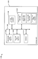
도 9 는 통신 링크에서 커넥터들의 아날로그 거동들을 모델링하고 시뮬레이션할 수 있는 프로세싱 회로 또는 시스템 (902) 의 예 (900) 를 예시하는 단순화된 블록 다이어그램이다. 프로세싱 회로 (902) 는 디지털 시스템 또는 디지털 컴포넌트들 (914) 의 거동을 시뮬레이션하는 소프트웨어를 포함하는 시뮬레이션 툴 (904) 을 포함할 수도 있다. 시뮬레이션 툴 (904) 은 기능성을 검증하기 위해 제조 전에 하드웨어를 검증하는데 이용될 수도 있다. 본 명세서에서 설명된 소정의 양태들에 따른 시뮬레이션 툴 (904) 은 커넥터들을 통해 송신된 신호들에 부가적으로 커넥터들의 아날로그 거동을 모델링할 수 있다.9 is a simplified block diagram illustrating an example 900 of a processing circuit or
프로세싱 회로 (902) 는 다양한 타입들의 하드웨어 및 오퍼레이팅 시스템들을 포함할 수도 있다. 하나의 예에서, 프로세싱 회로 (902) 는 단일-보드 타입의 컴퓨터, 예컨대 제어기 또는 블레이드 서버, 데스크톱 컴퓨터, 윈도우즈-기반 시스템, 유닛스-기반 시스템, 선 솔라리스 (Sun Solaris) 시스템, 리눅스-기반 시스템, 다수의 컴퓨팅 디바이스들을 갖는 분산 시스템 등으로부터 적응될 수도 있다. 시뮬레이션 툴 (904) 은 하나 이상의 프로세싱 회로들 (902) 과 협력하거나 또는 이 프로세싱 회로들 상에서 실행하는 하드웨어 및 소프트웨어의 일부 조합으로서 구현될 수도 있다. 시뮬레이션 툴 (904) 은 하나 이상의 실행가능한 프로그램들, 라이브러리들 및/또는 데이터의 세트들을 포함할 수도 있다.The
시뮬레이션 툴 (904) 은 통신 링크들에 부가적으로 디지털 시스템들 및/또는 디지털 컴포넌트들을 시뮬레이션하는데 이용될 수도 있다. 예를 들어, 시뮬레이션 툴 (904) 은 셀룰러 폰 내의 디지털 회로를 시뮬레이션하는데 이용될 수도 있다. 시뮬레이션 툴 (904) 은 디지털 컴포넌트들 및/또는 블록들 (914) 을 모델링하거나 또는 그렇지 않으면 표현할 수도 있다. 디지털 컴포넌트들 (914) 은 집적 회로 디바이스들, 트랜지스터들, 디지털 로직 빌딩 블록들 예컨대 로직 게이트들 등을 포함할 수도 있다. 시뮬레이션 툴 (904) 은 통신 링크의 하나 이상의 커넥터들 (910) 을 모델링하거나 또는 그렇지 않으면 표현할 수도 있고 또는 소정의 디지털 컴포넌트들 (914) 간에서 상호연결할 수도 있다. 시뮬레이션 툴 (904) 은 통신 링크의 커넥터들 (910) 을 통해 송신되는 신호들을 포함하는 하나 이상의 신호들 (912) 을 모델링하거나 또는 그렇지 않으면 표현할 수도 있고 또는 소정의 디지털 컴포넌트들 (914) 간에서 상호연결할 수도 있다. 시뮬레이션 툴 (904) 은 하나 이상의 클록 신호들 또는 사이클들, 수동 아날로그 컴포넌트들 등을 포함하는 다른 컴포넌트들을 모델링하거나 또는 그렇지 않으면 표현할 수도 있다. 시뮬레이션 툴 (904) 은 디지털 컴포넌트들 (914), 신호들 (912) 및/또는 커넥터들 (910) 에 의해 이용된 클록 신호들 또는 사이클들을 시뮬레이션하는데 이용될 수 있는 하나 이상의 스케줄러들 (916) 을 모델링하거나 또는 그렇지 않으면 표현할 수도 있다.The
도 10 은 본 발명의 소정의 양태들에 따른 인코딩 방법을 예시하는 플로우차트이다. 이 방법은 시뮬레이션 툴 또는 테스트 디바이스에 의해 수행될 수도 있다.10 is a flow chart illustrating an encoding method in accordance with certain aspects of the present invention. This method may be performed by a simulation tool or a test device.
단계 1002 에서, 디바이스는 통신 링크에서의 물리적 연결을 표현하는 디지털 신호를 생성할 수도 있다.In
단계 1004 에서, 디바이스는 물리적 연결을 통해 송신되는 3-위상 신호를 특성화하는 가상 신호를 생성할 수도 있다. 하나의 예에서, 통신 링크는 3 개의 물리적 연결들을 포함하고, 각각의 물리적 연결은 액티브 동작 모드가 선택될 때 3-위상 신호의 상이한 위상을 통신한다. 3 개의 물리적 연결들 각각은 인액티브 동작 모드에서 하이-임피던스 상태에 있을 수도 있다.In
단계 1006 에서, 디바이스는 물리적 연결의 하나 이상의 아날로그 특성들을 모델링하도록 가상 신호를 구성할 수도 있다. 아날로그 특성들은 3-위상 신호를 정의하는 전압 상태들을 포함할 수도 있다. 물리적 연결의 아날로그 특성들은 3-위상 신호의 시그널링 상태들에 대응하는 적어도 3 개의 전압 상태들을 포함할 수도 있다. 전압 상태들은 적어도 3 개의 유효 전압 상태들을 포함할 수도 있다. 전압 상태 각각은 물리적 연결과 연관된 전압 레벨에 대응할 수도 있다.At
소정의 양태들에 따르면, 적어도 3 개의 유효 전압 상태들 중 하나는 미구동된 상태를 포함한다. 통신 링크가 액티브 동작 모드에 있을 때 통신 링크에서 하나의 물리적 연결만이 미구동된 상태에 유효하게 있을 수도 있다. 가상 신호는 물리적 연결의 하나 이상의 동작 모드들 간에서 선택할 수도 있다. 물리적 연결은 인액티브 동작 모드가 선택될 때 하이-임피던스 상태 또는 미정의된 상태에 있을 수도 있다. 동작 모드들은 고속 모드 및 저속 모드를 포함한다. 디지털 신호는 제 1 전압 상태와 제 2 전압 상태 사이에서 선택하는 제 1 바이너리 비트를 포함할 수도 있다. 제 2 전압 상태의 전압 레벨은 가상 신호에 의해 선택된다.According to certain aspects, one of the at least three valid voltage states comprises an undriven state. Only one physical connection on the communication link may be valid for an undriven state when the communication link is in the active mode of operation. The virtual signal may be selected between one or more operating modes of the physical connection. The physical connection may be in a high-impedance state or an undefined state when the inactive operation mode is selected. The operating modes include a high speed mode and a low speed mode. The digital signal may comprise a first binary bit to select between a first voltage state and a second voltage state. The voltage level of the second voltage state is selected by the virtual signal.
소정의 양태들에 따르면, 3-위상 신호는 최대 전압 레벨과 최소 전압 레벨에 의해 경계지어진 전압 범위 내에서 스위칭할 수도 있다. 제 1 전압 상태는 최소 전압 레벨로서 정의될 수도 있다. 제 2 전압 상태의 전압 레벨은, 최소 전압 레벨보다 더 크고 최대 전압 레벨보다 더 작은 중간 전압 레벨 또는 최대 전압 레벨 중 어느 하나로서 가상 신호에 의해 선택될 수도 있다.According to certain aspects, the 3-phase signal may switch within a voltage range bounded by a maximum voltage level and a minimum voltage level. The first voltage state may be defined as the minimum voltage level. The voltage level of the second voltage state may be selected by the virtual signal as either an intermediate voltage level or a maximum voltage level which is greater than the minimum voltage level and smaller than the maximum voltage level.
소정의 양태들에 따르면, 3-위상 신호는 최대 전압 레벨과 최소 전압 레벨에 의해 경계지어진 전압 범위 내에서 스위칭한다. 제 1 전압 상태는 최대 전압 레벨로서 정의될 수도 있다. 제 2 전압 상태의 전압 레벨은, 최소 전압 레벨보다 더 크고 최대 전압 레벨보다 더 작은 중간 전압 레벨 또는 최소 전압 레벨 중 어느 하나로서 가상 신호에 의해 선택될 수도 있다.According to certain aspects, the three-phase signal switches within a voltage range bounded by a maximum voltage level and a minimum voltage level. The first voltage state may be defined as the maximum voltage level. The voltage level of the second voltage state may be selected by a virtual signal as either an intermediate voltage level or a minimum voltage level which is greater than the minimum voltage level and smaller than the maximum voltage level.
소정의 양태들에 따르면, 가상 신호는, 통신 링크가 저속 동작 모드들에서 동작될 때의 물리적 연결의 상이한 아날로그 거동들인, 통신 링크가 고속 모드에서 동작될 때의 물리적 연결의 아날로그 거동들을 특성화한다. 물리적 연결의 아날로그 거동들은 물리적 연결에 대한 신호 상태들 간의 상승 시간 또는 상승 시간의 레이트를 포함할 수도 있다.According to certain aspects, the virtual signal characterizes the analog behaviors of the physical connection when the communication link is operated in the high speed mode, which are the different analog behaviors of the physical connection when the communication link is operated in the low speed operation modes. The analog behaviors of a physical connection may include the rate of rise time or rise time between signal states for a physical connection.
도 11 은 프로세싱 시스템 (1102) 을 채용한 장치에 대한 하드웨어 구현의 단순화된 예를 예시하는 다이어그램 (1100) 이다. 프로세싱 회로 (1102) 는 버스 (1120) 에 의해 일반적으로 표현되는 버스 아키텍처로 구현될 수도 있다. 버스 (1120) 는 프로세싱 회로 (1102) 의 특정 애플리케이션 및 전체 설계 제약들에 의존하는 임의의 개수의 상호연결 버스들 및 브리지들을 포함할 수도 있다. 버스 (1120) 는 프로세서 (1116), 모듈들 또는 회로들 (1104, 1106, 1108, 1112), 및 컴퓨터 판독가능 저장 매체 (1118) 에 의해 표현된 하나 이상의 프로세서들 및/또는 하드웨어 모듈들을 포함하는 다양한 회로들을 함께 링크시킨다. 버스 (1120) 는 또한, 당업계에 널리 공지되고 따라서 더 이상 설명되지 않을 타이밍 소스들, 주변기기들, 전압 레귤레이터들, 및 전력 관리 회로들과 같은 다양한 다른 회로들을 링크시킬 수도 있다.11 is a diagram 1100 illustrating a simplified example of a hardware implementation for an apparatus employing the
프로세서 (1116) 는 마이크로프로세서, 제어기, 디지털 신호 프로세서, 시퀀서, 상태 머신 등을 포함할 수도 있다. 프로세서 (1116) 는 컴퓨터 판독가능 저장 매체 (1116) 상에 저장된 소프트웨어의 실행을 포함하는 일반 프로세싱을 담당한다. 소프트웨어는, 프로세서 (1116) 에 의해 실행될 경우, 프로세싱 회로 (1102) 로 하여금 임의의 특정 장치에 대해 상기 설명된 다양한 기능들을 수행하게 한다. 컴퓨터 판독가능 저장 매체 (1118) 는 또한, 소프트웨어를 실행할 때 프로세서 (1116) 에 의해 조작되는 데이터를 저장하는데 이용될 수도 있다. 프로세싱 회로 (1102) 는 모듈들 (1104, 1106 및 1108) 중 적어도 하나를 더 포함한다. 이 모듈들 (1104, 1106 및/또는 1108) 은 컴퓨터 판독가능 저장 매체 (1118) 에 상주/저장된, 프로세서 (1116) 에서 실행하는 소프트웨어 모듈들, 프로세서 (1116) 에 커플링된 하나 이상의 하드웨어 모듈들, 또는 이들의 일부 조합일 수도 있다.The
하나의 구성에서, 장치 (1100) 는 통신 링크에서의 물리적 연결을 표현하는 디지털 신호를 생성하기 위한 모듈들 또는 회로 (1104), 물리적 연결을 통해 송신되는 3-위상 신호를 특성화하는 가상 신호를 생성하기 위한 모듈들 또는 회로 (1106), 가상 신호가 물리적 연결의 하나 이상의 아날로그 특성들을 모델링하도록 구성하기 위한 모듈들 또는 회로 (1108) 를 포함한다.In one configuration, the
개시된 프로세스들에서의 단계들의 특정 순서 또는 계층구조가 예시적인 접근법들의 일 예시임이 이해된다. 설계 선호도들에 기초하여, 프로세스들에서의 단계들의 특정 순서 또는 계층구조가 재배열될 수도 있음이 이해된다. 첨부한 방법 청구항들은, 샘플 순서로 다양한 단계들의 엘리먼트들을 제시하며, 제시된 특정 순서 또는 계층구조로 제한되도록 의도되지 않는다.It is understood that the particular order or hierarchy of steps in the disclosed processes is one example of exemplary approaches. It is understood that, based on design preferences, a particular order or hierarchy of steps in the processes may be rearranged. The appended method claims present elements of the various steps in a sample order and are not intended to be limited to the specific order or hierarchy presented.
이전 설명은 당업자로 하여금 본 명세서에 설명된 다양한 양태들을 실시할 수 있게 하도록 제공된다. 이들 양태들에 대한 다양한 수정들은 당업자들에게 쉽게 명백할 것이며, 본 명세서에 정의된 일반 원리들은 다른 양태들에 적용될 수도 있다. 따라서, 청구항들은 본 명세서에 나타낸 양태들로 제한되도록 의도되지 않지만, 문언적 청구항들과 부합하는 전체 범위를 부여받으려는 것으로, 여기서 단수로의 엘리먼트들에 대한 언급은 구체적으로 그렇게 서술되지 않는다면 "하나 그리고 단지 하나만" 을 의미하도록 의도되지 않고 오히려 "하나 이상" 을 의미하도록 의도된다. 구체적으로 달리 서술되지 않는다면, 용어 "일부" 는 하나 이상을 지칭한다. 당업자들에게 공지되어 있거나 추후에 공지되게 되는 본 개시물 전반에 걸쳐 설명된 다양한 양태들의 엘리먼트들에 대한 모든 구조적 및 기능적 균등물들은 본 명세서에 참조로 명백히 포함되고 청구항들에 의해 포괄되도록 의도된다. 더욱이, 본 명세서에 개시된 어떤 것도, 그러한 개시물이 청구항들에 명시적으로 상술되는지 여부에 상관없이 공중에 받쳐지도록 의도되지 않는다. 어떠한 청구항 요소도, 그 요소가 어구 "하는 수단" 을 사용하여 명백히 인용되지 않는다면 기능식 (means plus function) 으로서 해석되지 않아야 한다.The previous description is provided to enable those skilled in the art to practice the various aspects described herein. Various modifications to these aspects will be readily apparent to those skilled in the art, and the generic principles defined herein may be applied to other aspects. Accordingly, the claims are not intended to be limited to the aspects shown herein, but are intended to be given the full breadth of conformity with literal claims, wherein references to elements in singular < RTI ID = 0.0 >Quot; one ", rather than " one " Unless specifically stated otherwise, the term "part" refers to one or more. All structural and functional equivalents to the elements of the various aspects described throughout this disclosure, which are known to those skilled in the art or which will be known in the future, are expressly incorporated herein by reference and are intended to be encompassed by the claims. Moreover, nothing disclosed herein is intended to be adorned with any such disclosure whether or not such disclosure is expressly set forth in the claims. No claim element shall be construed as a means plus function unless the element is expressly recited using the phrase "means of ".
Claims (48)
상기 가상 신호는 상기 물리적 연결의 하나 이상의 아날로그 특성들을 표현하고,
상기 아날로그 특성들은 상기 3-위상 신호를 정의하는 전압 상태들을 포함하는, 장치.At least one processing circuit configured to generate a digital signal representative of a physical connection in a communication link and a virtual signal characterizing a three-phase signal transmitted over the physical connection,
The virtual signal representing one or more analog characteristics of the physical connection,
Wherein the analog characteristics include voltage states that define the three-phase signal.
상기 전압 상태들은 적어도 3 개의 유효 전압 상태들을 포함하고, 각각의 전압 상태는 상기 물리적 연결과 연관된 전압 레벨에 대응하는, 장치.The method according to claim 1,
Wherein the voltage states comprise at least three valid voltage states and wherein each voltage state corresponds to a voltage level associated with the physical connection.
상기 적어도 3 개의 유효 전압 상태들 중 하나는 미구동된 (undriven) 상태를 포함하고, 상기 통신 링크가 액티브 (active) 동작 모드에 있을 때 상기 통신 링크에서의 하나의 물리적 연결만이 상기 미구동된 상태에 있는, 장치.3. The method of claim 2,
Wherein one of the at least three valid voltage states comprises an undriven state and wherein when only one physical connection on the communication link is in the undriven state when the communication link is in an active operational mode, The device in the state.
상기 가상 신호는 상기 물리적 연결의 하나 이상의 동작 모드들 간에서 선택하고, 상기 물리적 연결은 인액티브 (inactive) 동작 모드가 선택될 때 하이-임피던스 상태 또는 미정의된 상태에 있는, 장치.3. The method of claim 2,
Wherein the virtual signal is selected between one or more modes of operation of the physical connection and the physical connection is in a high-impedance or undefined state when an inactive mode of operation is selected.
상기 통신 링크는 3 개의 물리적 연결들을 포함하고, 액티브 동작 모드가 선택될 때 각각의 물리적 연결은 상기 3-위상 신호의 상이한 위상을 통신하고, 상기 3 개의 물리적 연결들 각각은 상기 인액티브 동작 모드에서 상기 하이-임피던스 상태에 있는, 장치.5. The method of claim 4,
Wherein the communication link comprises three physical connections, each physical connection communicating a different phase of the three-phase signal when an active mode of operation is selected, and each of the three physical connections is in an active mode of operation And wherein the device is in the high-impedance state.
상기 하나 이상의 동작 모드들은 고속 모드 및 저속 모드를 포함하는, 장치.5. The method of claim 4,
Wherein the one or more operating modes include a high speed mode and a low speed mode.
상기 디지털 신호는 제 1 전압 상태와 제 2 전압 상태 사이에서 선택하는 제 1 바이너리 비트를 포함하는, 장치.The method according to claim 1,
Wherein the digital signal comprises a first binary bit to select between a first voltage state and a second voltage state.
상기 제 2 전압 상태의 전압 레벨은 상기 가상 신호에 의해 선택되는, 장치.8. The method of claim 7,
And the voltage level of the second voltage state is selected by the virtual signal.
상기 3-위상 신호는 최대 전압 레벨과 최소 전압 레벨에 의해 경계지어진 전압 범위 내에서 스위칭하고;
상기 제 1 전압 상태는 상기 최소 전압 레벨로서 정의되며;
상기 제 2 전압 상태의 전압 레벨은, 상기 최소 전압 레벨보다 더 크고 상기 최대 전압 레벨보다 더 작은 중간 전압 레벨 또는 상기 최대 전압 레벨 중 어느 하나로서 상기 가상 신호에 의해 선택되는, 장치.8. The method of claim 7,
Said 3-phase signal switching within a voltage range bounded by a maximum voltage level and a minimum voltage level;
The first voltage state is defined as the minimum voltage level;
Wherein the voltage level of the second voltage state is selected by the virtual signal either as an intermediate voltage level that is greater than the minimum voltage level and less than the maximum voltage level, or as the maximum voltage level.
상기 3-위상 신호는 최대 전압 레벨과 최소 전압 레벨에 의해 경계지어진 전압 범위 내에서 스위칭하고;
상기 제 1 전압 상태는 상기 최대 전압 레벨로서 정의되며;
상기 제 2 전압 상태의 전압 레벨은, 상기 최소 전압 레벨보다 더 크고 상기 최대 전압 레벨보다 더 작은 중간 전압 레벨 또는 상기 최소 전압 레벨 중 어느 하나로서 상기 가상 신호에 의해 선택되는, 장치.8. The method of claim 7,
Said 3-phase signal switching within a voltage range bounded by a maximum voltage level and a minimum voltage level;
The first voltage state is defined as the maximum voltage level;
Wherein the voltage level of the second voltage state is selected by the virtual signal either as an intermediate voltage level that is greater than the minimum voltage level and less than the maximum voltage level or as the minimum voltage level.
상기 가상 신호는, 상기 통신 링크가 저속 동작 모드들에서 동작될 때의 상기 물리적 연결의 상이한 아날로그 거동들인, 상기 통신 링크가 고속 모드에서 동작될 때의 상기 물리적 연결의 아날로그 거동들을 특성화하는, 장치.The method according to claim 1,
Wherein the virtual signal characterizes analog behaviors of the physical connection when the communication link is operated in a high speed mode, wherein the communication links are different analog behaviors of the physical connection when operating in low speed modes of operation.
상기 물리적 연결의 아날로그 거동들은 상기 물리적 연결에 대한 신호 상태들 간의 상승 시간 또는 상승 시간의 레이트를 포함하는, 장치.12. The method of claim 11,
Wherein the analog behaviors of the physical connection include a rate of rise time or rise time between signal conditions for the physical connection.
통신 링크에서의 물리적 연결을 표현하는 디지털 신호를 생성하는 단계;
상기 물리적 연결을 통해 송신되는 3-위상 신호를 특성화하는 가상 신호를 생성하는 단계; 및
상기 가상 신호가 상기 물리적 연결의 하나 이상의 아날로그 특성들을 모델링하도록 구성하는 단계를 포함하고,
상기 아날로그 특성들은 상기 3-위상 신호를 정의하는 전압 상태들을 포함하고,
상기 물리적 연결의 아날로그 특성들은 상기 3-위상 신호의 시그널링 상태들에 대응하는 적어도 3 개의 전압 상태들을 포함하는, 디지털 시스템들을 시뮬레이션하는 방법.CLAIMS 1. A method for simulating digital systems,
Generating a digital signal representing a physical connection in the communication link;
Generating a virtual signal that characterizes a three-phase signal transmitted over the physical connection; And
And configuring the virtual signal to model one or more analog characteristics of the physical connection,
The analog characteristics comprising voltage states defining the three-phase signal,
Wherein analog characteristics of the physical connection comprise at least three voltage states corresponding to signaling states of the three-phase signal.
상기 전압 상태들은 적어도 3 개의 유효 전압 상태들을 포함하고, 각각의 전압 상태는 상기 물리적 연결과 연관된 전압 레벨에 대응하는, 디지털 시스템들을 시뮬레이션하는 방법.14. The method of claim 13,
Wherein the voltage states comprise at least three valid voltage states, and wherein each voltage state corresponds to a voltage level associated with the physical connection.
상기 적어도 3 개의 유효 전압 상태들 중 하나는 미구동된 상태를 포함하고, 상기 통신 링크가 액티브 동작 모드에 있을 때 상기 통신 링크에서의 하나의 물리적 연결만이 상기 미구동된 상태에 있는, 디지털 시스템들을 시뮬레이션하는 방법.15. The method of claim 14,
Wherein one of the at least three valid voltage states comprises an inactive state and only one physical connection at the communication link is in the undriven state when the communication link is in an active operational mode, Lt; / RTI >
상기 가상 신호는 상기 물리적 연결의 하나 이상의 동작 모드들 간에서 선택하고, 인액티브 동작 모드가 선택될 때 상기 물리적 연결은 하이-임피던스 상태 또는 미정의된 상태에 있는, 디지털 시스템들을 시뮬레이션하는 방법.15. The method of claim 14,
Wherein the virtual signal is selected between one or more operational modes of the physical connection and the physical connection is in a high-impedance state or an undetermined state when the inactive operational mode is selected.
상기 통신 링크는 3 개의 물리적 연결들을 포함하고, 액티브 동작 모드가 선택될 때 각각의 물리적 연결은 상기 3-위상 신호의 상이한 위상을 통신하고, 상기 3 개의 물리적 연결들 각각은 상기 인액티브 동작 모드에서 상기 하이-임피던스 상태에 있는, 디지털 시스템들을 시뮬레이션하는 방법.17. The method of claim 16,
Wherein the communication link comprises three physical connections, each physical connection communicating a different phase of the three-phase signal when an active mode of operation is selected, and each of the three physical connections is in an active mode of operation Wherein the high-impedance state is in the high-impedance state.
상기 하나 이상의 동작 모드들은 고속 모드 및 저속 모드를 포함하는, 디지털 시스템들을 시뮬레이션하는 방법.17. The method of claim 16,
Wherein the one or more operating modes include a high speed mode and a low speed mode.
상기 디지털 신호는 제 1 전압 상태와 제 2 전압 상태 사이에서 선택하는 제 1 바이너리 비트를 포함하는, 디지털 시스템들을 시뮬레이션하는 방법.14. The method of claim 13,
Wherein the digital signal comprises a first binary bit to select between a first voltage state and a second voltage state.
상기 제 2 전압 상태의 전압 레벨은 상기 가상 신호에 의해 선택되는, 디지털 시스템들을 시뮬레이션하는 방법.20. The method of claim 19,
Wherein the voltage level of the second voltage state is selected by the virtual signal.
상기 3-위상 신호는 최대 전압 레벨과 최소 전압 레벨에 의해 경계지어진 전압 범위 내에서 스위칭하고;
상기 제 1 전압 상태는 상기 최소 전압 레벨로서 정의되며;
상기 제 2 전압 상태의 전압 레벨은, 상기 최소 전압 레벨보다 더 크고 상기 최대 전압 레벨보다 더 작은 중간 전압 레벨 또는 상기 최대 전압 레벨 중 어느 하나로서 상기 가상 신호에 의해 선택되는, 디지털 시스템들을 시뮬레이션하는 방법.20. The method of claim 19,
Said 3-phase signal switching within a voltage range bounded by a maximum voltage level and a minimum voltage level;
The first voltage state is defined as the minimum voltage level;
Wherein the voltage level of the second voltage state is selected by the virtual signal either as an intermediate voltage level that is greater than the minimum voltage level and less than the maximum voltage level or as the maximum voltage level .
상기 3-위상 신호는 최대 전압 레벨과 최소 전압 레벨에 의해 경계지어진 전압 범위 내에서 스위칭하고;
상기 제 1 전압 상태는 상기 최대 전압 레벨로서 정의되며;
상기 제 2 전압 상태의 전압 레벨은, 상기 최소 전압 레벨보다 더 크고 상기 최대 전압 레벨보다 더 작은 중간 전압 레벨 또는 상기 최소 전압 레벨 중 어느 하나로서 상기 가상 신호에 의해 선택되는, 디지털 시스템들을 시뮬레이션하는 방법.20. The method of claim 19,
Said 3-phase signal switching within a voltage range bounded by a maximum voltage level and a minimum voltage level;
The first voltage state is defined as the maximum voltage level;
Wherein the voltage level of the second voltage state is selected by the virtual signal either as an intermediate voltage level which is greater than the minimum voltage level and less than the maximum voltage level or as the minimum voltage level .
상기 가상 신호는, 상기 통신 링크가 저속 동작 모드들에서 동작될 때의 상기 물리적 연결의 상이한 아날로그 거동들인, 상기 통신 링크가 고속 모드에서 동작될 때의 상기 물리적 연결의 아날로그 거동들을 특성화하는, 디지털 시스템들을 시뮬레이션하는 방법.14. The method of claim 13,
Wherein the virtual signal characterizes analog behaviors of the physical connection when the communication link is operated in the high speed mode, wherein the communication links are different analog behaviors of the physical connection when operating in low speed operation modes. Lt; / RTI >
상기 물리적 연결의 아날로그 거동들은 상기 물리적 연결에 대한 신호 상태들 간의 상승 시간 또는 상승 시간의 레이트를 포함하는, 디지털 시스템들을 시뮬레이션하는 방법.24. The method of claim 23,
Wherein the analog behaviors of the physical connection include a rate of rise time or rise time between signal states for the physical connection.
상기 물리적 연결을 통해 송신되는 3-위상 신호를 특성화하는 가상 신호를 생성하는 수단; 및
상기 가상 신호가 상기 물리적 연결의 하나 이상의 아날로그 특성들을 모델링하도록 구성하는 수단을 포함하고,
상기 아날로그 특성들은 상기 3-위상 신호를 정의하는 전압 상태들을 포함하고,
상기 물리적 연결의 아날로그 특성들은 상기 3-위상 신호의 시그널링 상태들에 대응하는 적어도 3 개의 전압 상태들을 포함하는, 장치.Means for generating a digital signal representative of a physical connection in a communication link;
Means for generating a virtual signal characterizing a three-phase signal transmitted over the physical connection; And
And means for configuring the virtual signal to model one or more analog characteristics of the physical connection,
The analog characteristics comprising voltage states defining the three-phase signal,
Wherein analog characteristics of the physical connection comprise at least three voltage states corresponding to signaling states of the three-phase signal.
상기 전압 상태들은 적어도 3 개의 유효 전압 상태들을 포함하고, 각각의 전압 상태는 상기 물리적 연결과 연관된 전압 레벨에 대응하는, 장치.26. The method of claim 25,
Wherein the voltage states comprise at least three valid voltage states and wherein each voltage state corresponds to a voltage level associated with the physical connection.
상기 적어도 3 개의 유효 전압 상태들 중 하나는 미구동된 상태를 포함하고, 상기 통신 링크가 액티브 동작 모드에 있을 때 상기 통신 링크에서의 하나의 물리적 연결만이 상기 미구동된 상태에 있는, 장치.27. The method of claim 26,
Wherein one of the at least three valid voltage states comprises an undriven state and only one physical connection at the communication link is in the undriven state when the communication link is in an active operational mode.
상기 가상 신호는 상기 물리적 연결의 하나 이상의 동작 모드들 간에서 선택하고, 인액티브 동작 모드가 선택될 때 상기 물리적 연결은 하이-임피던스 상태 또는 미정의된 상태에 있는, 장치.27. The method of claim 26,
Wherein the virtual signal is selected between one or more modes of operation of the physical connection and the physical connection is in a high-impedance state or an undetermined state when the inactive mode of operation is selected.
상기 통신 링크는 3 개의 물리적 연결들을 포함하고, 액티브 동작 모드가 선택될 때 각각의 물리적 연결은 상기 3-위상 신호의 상이한 위상을 통신하고, 상기 3 개의 물리적 연결들 각각은 상기 인액티브 동작 모드에서 상기 하이-임피던스 상태에 있는, 장치.29. The method of claim 28,
Wherein the communication link comprises three physical connections, each physical connection communicating a different phase of the three-phase signal when an active mode of operation is selected, and each of the three physical connections is in an active mode of operation And wherein the device is in the high-impedance state.
상기 하나 이상의 동작 모드들은 고속 모드 및 저속 모드를 포함하는, 장치.29. The method of claim 28,
Wherein the one or more operating modes include a high speed mode and a low speed mode.
상기 디지털 신호는 제 1 전압 상태와 제 2 전압 상태 사이에서 선택하는 제 1 바이너리 비트를 포함하는, 장치.26. The method of claim 25,
Wherein the digital signal comprises a first binary bit to select between a first voltage state and a second voltage state.
상기 제 2 전압 상태의 전압 레벨은 상기 가상 신호에 의해 선택되는, 장치.32. The method of claim 31,
And the voltage level of the second voltage state is selected by the virtual signal.
상기 3-위상 신호는 최대 전압 레벨과 최소 전압 레벨에 의해 경계지어진 전압 범위 내에서 스위칭하고;
상기 제 1 전압 상태는 상기 최소 전압 레벨로서 정의되며;
상기 제 2 전압 상태의 전압 레벨은, 상기 최소 전압 레벨보다 더 크고 상기 최대 전압 레벨보다 더 작은 중간 전압 레벨 또는 상기 최대 전압 레벨 중 어느 하나로서 상기 가상 신호에 의해 선택되는, 장치.32. The method of claim 31,
Said 3-phase signal switching within a voltage range bounded by a maximum voltage level and a minimum voltage level;
The first voltage state is defined as the minimum voltage level;
Wherein the voltage level of the second voltage state is selected by the virtual signal either as an intermediate voltage level that is greater than the minimum voltage level and less than the maximum voltage level, or as the maximum voltage level.
상기 3-위상 신호는 최대 전압 레벨과 최소 전압 레벨에 의해 경계지어진 전압 범위 내에서 스위칭하고;
상기 제 1 전압 상태는 상기 최대 전압 레벨로서 정의되며;
상기 제 2 전압 상태의 전압 레벨은, 상기 최소 전압 레벨보다 더 크고 상기 최대 전압 레벨보다 더 작은 중간 전압 레벨 또는 상기 최소 전압 레벨 중 어느 하나로서 상기 가상 신호에 의해 선택되는, 장치.32. The method of claim 31,
Said 3-phase signal switching within a voltage range bounded by a maximum voltage level and a minimum voltage level;
The first voltage state is defined as the maximum voltage level;
Wherein the voltage level of the second voltage state is selected by the virtual signal either as an intermediate voltage level that is greater than the minimum voltage level and less than the maximum voltage level or as the minimum voltage level.
상기 가상 신호는, 상기 통신 링크가 저속 동작 모드들에서 동작될 때의 상기 물리적 연결의 상이한 아날로그 거동들인, 상기 통신 링크가 고속 모드에서 동작될 때의 상기 물리적 연결의 아날로그 거동들을 특성화하는, 장치.26. The method of claim 25,
Wherein the virtual signal characterizes analog behaviors of the physical connection when the communication link is operated in a high speed mode, wherein the communication links are different analog behaviors of the physical connection when operating in low speed modes of operation.
상기 물리적 연결의 아날로그 거동들은 상기 물리적 연결에 대한 신호 상태들 간의 상승 시간 또는 상승 시간의 레이트를 포함하는, 장치.36. The method of claim 35,
Wherein the analog behaviors of the physical connection include a rate of rise time or rise time between signal conditions for the physical connection.
적어도 하나의 프로세싱 회로; 및
프로세서와 전자 통신하는 프로세서 판독가능 저장 매체를 포함하고,
상기 프로세서 판독가능 저장 매체는 하나 이상의 명령들을 가지며,
상기 명령들은, 상기 적어도 하나의 프로세싱 회로에 의해 실행될 때, 상기 적어도 하나의 프로세싱 회로로 하여금,
통신 링크에서의 물리적 연결을 표현하는 디지털 신호를 생성하게 하고;
상기 물리적 연결을 통해 송신되는 3-위상 신호를 특성화하는 가상 신호를 생성하게 하며;
상기 물리적 연결의 하나 이상의 아날로그 특성들을 모델링하도록 상기 가상 신호를 구성하게 하고,
상기 아날로그 특성들은 상기 3-위상 신호를 정의하는 전압 상태들을 포함하고,
상기 물리적 연결의 아날로그 특성들은 상기 3-위상 신호의 시그널링 상태들에 대응하는 적어도 3 개의 전압 상태들을 포함하는, 디지털 시스템들을 시뮬레이션하기 위한 장치.An apparatus for simulating digital systems,
At least one processing circuit; And
A processor readable storage medium in electronic communication with the processor,
The processor readable storage medium having one or more instructions,
Wherein the instructions cause the at least one processing circuit to, when executed by the at least one processing circuit,
Generate a digital signal representative of a physical connection in a communication link;
Generate a virtual signal that characterizes a three-phase signal transmitted over the physical connection;
Configure the virtual signal to model one or more analog characteristics of the physical connection,
The analog characteristics comprising voltage states defining the three-phase signal,
Wherein analog characteristics of the physical connection comprise at least three voltage states corresponding to signaling states of the three-phase signal.
상기 전압 상태들은 적어도 3 개의 유효 전압 상태들을 포함하고, 각각의 전압 상태는 상기 물리적 연결과 연관된 전압 레벨에 대응하는, 디지털 시스템들을 시뮬레이션하기 위한 장치.39. The method of claim 37,
Wherein the voltage states comprise at least three valid voltage states and wherein each voltage state corresponds to a voltage level associated with the physical connection.
상기 적어도 3 개의 유효 전압 상태들 중 하나는 미구동된 상태를 포함하고, 상기 통신 링크가 액티브 동작 모드에 있을 때 상기 통신 링크에서의 하나의 물리적 연결만이 상기 미구동된 상태에 있는, 디지털 시스템들을 시뮬레이션하기 위한 장치.39. The method of claim 38,
Wherein one of the at least three valid voltage states comprises an inactive state and only one physical connection at the communication link is in the undriven state when the communication link is in an active operational mode, Lt; / RTI >
상기 가상 신호는 상기 물리적 연결의 하나 이상의 동작 모드들 간에서 선택하고, 인액티브 동작 모드가 선택될 때 상기 물리적 연결은 하이-임피던스 상태 또는 미정의된 상태에 있는, 디지털 시스템들을 시뮬레이션하기 위한 장치.39. The method of claim 38,
Wherein the virtual signal is selected between one or more modes of operation of the physical connection, and when the inactive mode of operation is selected, the physical connection is in a high-impedance state or an undetermined state.
상기 통신 링크는 3 개의 물리적 연결들을 포함하고, 액티브 동작 모드가 선택될 때 각각의 물리적 연결은 상기 3-위상 신호의 상이한 위상을 통신하고, 상기 3 개의 물리적 연결들 각각은 상기 인액티브 동작 모드에서 상기 하이-임피던스 상태에 있는, 디지털 시스템들을 시뮬레이션하기 위한 장치.41. The method of claim 40,
Wherein the communication link comprises three physical connections, each physical connection communicating a different phase of the three-phase signal when an active mode of operation is selected, and each of the three physical connections is in an active mode of operation Wherein the high-impedance state is in the high-impedance state.
상기 하나 이상의 동작 모드들은 고속 모드 및 저속 모드를 포함하는, 디지털 시스템들을 시뮬레이션하기 위한 장치.41. The method of claim 40,
Wherein the one or more operating modes include a high speed mode and a low speed mode.
상기 디지털 신호는 제 1 전압 상태와 제 2 전압 상태 사이에서 선택하는 제 1 바이너리 비트를 포함하는, 디지털 시스템들을 시뮬레이션하기 위한 장치.39. The method of claim 37,
Wherein the digital signal comprises a first binary bit to select between a first voltage state and a second voltage state.
상기 제 2 전압 상태의 전압 레벨은 상기 가상 신호에 의해 선택되는, 디지털 시스템들을 시뮬레이션하기 위한 장치.44. The method of claim 43,
And wherein the voltage level of the second voltage state is selected by the virtual signal.
상기 3-위상 신호는 최대 전압 레벨과 최소 전압 레벨에 의해 경계지어진 전압 범위 내에서 스위칭하고;
상기 제 1 전압 상태는 상기 최소 전압 레벨로서 정의되며;
상기 제 2 전압 상태의 전압 레벨은, 상기 최소 전압 레벨보다 더 크고 상기 최대 전압 레벨보다 더 작은 중간 전압 레벨 또는 상기 최대 전압 레벨 중 어느 하나로서 상기 가상 신호에 의해 선택되는, 디지털 시스템들을 시뮬레이션하기 위한 장치.44. The method of claim 43,
Said 3-phase signal switching within a voltage range bounded by a maximum voltage level and a minimum voltage level;
The first voltage state is defined as the minimum voltage level;
Wherein the voltage level of the second voltage state is selected by the virtual signal either as an intermediate voltage level that is greater than the minimum voltage level and less than the maximum voltage level or as the maximum voltage level. Device.
상기 3-위상 신호는 최대 전압 레벨과 최소 전압 레벨에 의해 경계지어진 전압 범위 내에서 스위칭하고;
상기 제 1 전압 상태는 상기 최대 전압 레벨로서 정의되며;
상기 제 2 전압 상태의 전압 레벨은, 상기 최소 전압 레벨보다 더 크고 상기 최대 전압 레벨보다 더 작은 중간 전압 레벨 또는 상기 최소 전압 레벨 중 어느 하나로서 상기 가상 신호에 의해 선택되는, 디지털 시스템들을 시뮬레이션하기 위한 장치.44. The method of claim 43,
Said 3-phase signal switching within a voltage range bounded by a maximum voltage level and a minimum voltage level;
The first voltage state is defined as the maximum voltage level;
Wherein the voltage level of the second voltage state is selected by the virtual signal either as an intermediate voltage level that is greater than the minimum voltage level and less than the maximum voltage level or as the minimum voltage level. Device.
상기 가상 신호는, 상기 통신 링크가 저속 동작 모드들에서 동작될 때의 상기 물리적 연결의 상이한 아날로그 거동들인, 상기 통신 링크가 고속 모드에서 동작될 때의 상기 물리적 연결의 아날로그 거동들을 특성화하는, 디지털 시스템들을 시뮬레이션하기 위한 장치.39. The method of claim 37,
Wherein the virtual signal characterizes analog behaviors of the physical connection when the communication link is operated in the high speed mode, wherein the communication links are different analog behaviors of the physical connection when operating in low speed operation modes. Lt; / RTI >
상기 물리적 연결의 아날로그 거동들은 상기 물리적 연결에 대한 신호 상태들 간의 상승 시간 또는 상승 시간의 레이트를 포함하는, 디지털 시스템들을 시뮬레이션하기 위한 장치.49. The method of claim 47,
Wherein the analog behaviors of the physical connection include a rate of rise time or rise time between signal states for the physical connection.
Applications Claiming Priority (3)
| Application Number | Priority Date | Filing Date | Title |
|---|---|---|---|
| US14/156,329 | 2014-01-15 | ||
| US14/156,329 US9961174B2 (en) | 2014-01-15 | 2014-01-15 | Analog behavior modeling for 3-phase signaling |
| PCT/US2015/011142 WO2015108847A1 (en) | 2014-01-15 | 2015-01-13 | Analog behavior modeling for 3-phase signaling |
Publications (1)
| Publication Number | Publication Date |
|---|---|
| KR20160108423A true KR20160108423A (en) | 2016-09-19 |
Family
ID=52450578
Family Applications (1)
| Application Number | Title | Priority Date | Filing Date |
|---|---|---|---|
| KR1020167021576A KR20160108423A (en) | 2014-01-15 | 2015-01-13 | Analog behavior modeling for 3-phase signaling |
Country Status (6)
| Country | Link |
|---|---|
| US (2) | US9961174B2 (en) |
| EP (1) | EP3095218A1 (en) |
| JP (1) | JP2017507556A (en) |
| KR (1) | KR20160108423A (en) |
| CN (1) | CN106416159B (en) |
| WO (1) | WO2015108847A1 (en) |
Families Citing this family (10)
| Publication number | Priority date | Publication date | Assignee | Title |
|---|---|---|---|---|
| US9584227B2 (en) * | 2015-07-17 | 2017-02-28 | Qualcomm Incorporated | Low-power mode signal bridge for optical media |
| US10554234B2 (en) | 2016-03-14 | 2020-02-04 | Sony Corporation | Transmission device, transmission method, and communication system |
| US10705894B2 (en) | 2016-05-30 | 2020-07-07 | Samsung Electronics Co., Ltd. | Electronic device for authenticating application and operating method thereof |
| US10419246B2 (en) * | 2016-08-31 | 2019-09-17 | Qualcomm Incorporated | C-PHY training pattern for adaptive equalization, adaptive edge tracking and delay calibration |
| KR20180061560A (en) | 2016-11-29 | 2018-06-08 | 삼성전자주식회사 | Electronic circuit adjusting delay depending on communication condition |
| US11748539B1 (en) * | 2017-09-28 | 2023-09-05 | Cadence Design Systems, Inc. | Converting analog variable delay in real number modeling code to cycle-driven simulation interface code |
| US11442098B2 (en) * | 2019-06-20 | 2022-09-13 | Teradyne, Inc. | Generating a waveform based on digital pulses |
| US11108604B2 (en) * | 2019-08-19 | 2021-08-31 | Qualcomm Incorporated | Driver architecture for multiphase and amplitude encoding transmitters |
| KR20210089811A (en) * | 2020-01-08 | 2021-07-19 | 삼성전자주식회사 | Electronic device detecting change of power mode based on external signal |
| US11757611B2 (en) | 2021-04-11 | 2023-09-12 | Litrinium, Inc. | PAM4 threshold phase engine |
Family Cites Families (24)
| Publication number | Priority date | Publication date | Assignee | Title |
|---|---|---|---|---|
| US5452231A (en) | 1988-10-05 | 1995-09-19 | Quickturn Design Systems, Inc. | Hierarchically connected reconfigurable logic assembly |
| US6675328B1 (en) * | 1999-10-08 | 2004-01-06 | Vigilant Networks, Llc | System and method to determine data throughput in a communication network |
| US6980644B1 (en) * | 2000-05-12 | 2005-12-27 | National Semiconductor Corporation | System and method for adapting an analog echo canceller in a transceiver front end |
| US6725404B1 (en) * | 2000-05-26 | 2004-04-20 | International Business Machines Corporation | Evaluation of interconnect reliability using propagation delay through interconnect |
| US6760882B1 (en) * | 2000-09-19 | 2004-07-06 | Intel Corporation | Mode selection for data transmission in wireless communication channels based on statistical parameters |
| US7145411B1 (en) * | 2002-03-18 | 2006-12-05 | Applied Micro Circuits Corporation | Flexible differential interconnect cable with isolated high frequency electrical transmission line |
| JP4604627B2 (en) * | 2004-09-22 | 2011-01-05 | ソニー株式会社 | Encoder device and decoder device |
| JP4610380B2 (en) * | 2005-03-16 | 2011-01-12 | 三菱電機株式会社 | Power converter |
| US20070099586A1 (en) * | 2005-11-01 | 2007-05-03 | Silicon Laboratories Inc. | System and method for reducing spurious emissions in a wireless communication device including a testing apparatus |
| US20070129926A1 (en) | 2005-12-01 | 2007-06-07 | Verheyen Henry T | Hardware acceleration system for simulation of logic and memory |
| EP1936773A1 (en) * | 2006-12-22 | 2008-06-25 | Abb Research Ltd. | System and method to detect a forgotten safety ground of an electrical facility |
| US9711041B2 (en) * | 2012-03-16 | 2017-07-18 | Qualcomm Incorporated | N-phase polarity data transfer |
| US7492287B2 (en) * | 2007-05-23 | 2009-02-17 | Micron Technology, Inc. | Two-bit tri-level forced transition encoding |
| US8848810B2 (en) * | 2008-03-05 | 2014-09-30 | Qualcomm Incorporated | Multiple transmitter system and method |
| JP2010021789A (en) * | 2008-07-10 | 2010-01-28 | Toshiba Corp | Skew failure detection circuit and skew failure detection method |
| US8352793B2 (en) * | 2008-08-15 | 2013-01-08 | Apple Inc. | Device testing method and architecture |
| CN102209902A (en) | 2008-11-14 | 2011-10-05 | 泰拉丁公司 | Method and apparatus for testing electrical connections on a printed circuit board |
| US7978110B2 (en) * | 2009-05-11 | 2011-07-12 | Taiwan Semiconductor Manufacturing Company, Ltd. | Digital-to-analog converter |
| KR20110052205A (en) * | 2009-11-12 | 2011-05-18 | 삼성전자주식회사 | Transmitter only ic chip having external loopback test function and therefore external loopback test method |
| CA2825780A1 (en) | 2011-01-25 | 2012-08-02 | Power Analytics Corporation | Systems and methods for real-time dc microgrid power analytics for mission-critical power systems |
| EP2509314B1 (en) * | 2011-04-04 | 2019-12-04 | Interlemo Holding S.A. | Installation for conveying signals between a video camera equipment and a remote equipment |
| CN202403774U (en) | 2011-12-29 | 2012-08-29 | 兰州海默科技股份有限公司 | Multiphase flow simulated experiment signal generation device |
| US8996740B2 (en) * | 2012-06-29 | 2015-03-31 | Qualcomm Incorporated | N-phase polarity output pin mode multiplexer |
| US9317353B2 (en) * | 2013-12-26 | 2016-04-19 | Intel Corporation | Method, apparatus and system for performing voltage margining |
-
2014
- 2014-01-15 US US14/156,329 patent/US9961174B2/en not_active Expired - Fee Related
-
2015
- 2015-01-13 CN CN201580004629.6A patent/CN106416159B/en not_active Expired - Fee Related
- 2015-01-13 WO PCT/US2015/011142 patent/WO2015108847A1/en active Application Filing
- 2015-01-13 EP EP15702870.5A patent/EP3095218A1/en not_active Withdrawn
- 2015-01-13 JP JP2016546088A patent/JP2017507556A/en active Pending
- 2015-01-13 KR KR1020167021576A patent/KR20160108423A/en not_active Application Discontinuation
-
2017
- 2017-12-21 US US15/849,714 patent/US20180115637A1/en not_active Abandoned
Also Published As
| Publication number | Publication date |
|---|---|
| US9961174B2 (en) | 2018-05-01 |
| JP2017507556A (en) | 2017-03-16 |
| US20180115637A1 (en) | 2018-04-26 |
| US20150201052A1 (en) | 2015-07-16 |
| WO2015108847A1 (en) | 2015-07-23 |
| CN106416159A (en) | 2017-02-15 |
| CN106416159B (en) | 2020-03-03 |
| EP3095218A1 (en) | 2016-11-23 |
Similar Documents
| Publication | Publication Date | Title |
|---|---|---|
| CN106416159B (en) | Apparatus and method for emulating a digital system | |
| US9148198B1 (en) | Programmable pre-emphasis circuit for MIPI C-PHY | |
| JP6568247B2 (en) | N-phase signal transition alignment | |
| CN106464298B (en) | There is the device and method of more conducting wire signalings of matching propagation delay between conducting wire pair | |
| US9172426B2 (en) | Voltage mode driver circuit for N-phase systems | |
| CN107852382B (en) | Time-based equalization for C-PHY 3-phase transmitters | |
| KR102083044B1 (en) | N-phase polarity output pin mode multiplexer | |
| TWI678073B (en) | Calibration pattern and duty-cycle distortion correction for clock data recovery in a multi-wire, multi-phase interface | |
| US20150043358A1 (en) | Run-length detection and correction | |
| KR20160067990A (en) | Eye pattern triggering based on symbol transition | |
| JP2018526889A (en) | Method, apparatus and storage medium for adaptation to three-phase signal swap in a three-wire communication link between two integrated circuit devices | |
| TWI691168B (en) | C-PHY receiver equalization | |
| JP6219538B2 (en) | Clock recovery circuit for multiple wire data signals | |
| WO2015148506A1 (en) | Multi-wire electrical parameter measurements via test patterns | |
| TWI822732B (en) | Independent pair 3-phase eye sampling circuit | |
| CN107113259B (en) | Transmission device, transmission method, and communication system |
Legal Events
| Date | Code | Title | Description |
|---|---|---|---|
| WITN | Application deemed withdrawn, e.g. because no request for examination was filed or no examination fee was paid |