KR20160095731A - Package on package type stack package and method of manufacturing the same - Google Patents
Package on package type stack package and method of manufacturing the same Download PDFInfo
- Publication number
- KR20160095731A KR20160095731A KR1020150017066A KR20150017066A KR20160095731A KR 20160095731 A KR20160095731 A KR 20160095731A KR 1020150017066 A KR1020150017066 A KR 1020150017066A KR 20150017066 A KR20150017066 A KR 20150017066A KR 20160095731 A KR20160095731 A KR 20160095731A
- Authority
- KR
- South Korea
- Prior art keywords
- package
- semiconductor chip
- bonding
- electrodes
- bonding wires
- Prior art date
Links
Images


Classifications
-
- H—ELECTRICITY
- H01—ELECTRIC ELEMENTS
- H01L—SEMICONDUCTOR DEVICES NOT COVERED BY CLASS H10
- H01L25/00—Assemblies consisting of a plurality of individual semiconductor or other solid state devices ; Multistep manufacturing processes thereof
- H01L25/50—Multistep manufacturing processes of assemblies consisting of devices, each device being of a type provided for in group H01L27/00 or H01L29/00
-
- H—ELECTRICITY
- H01—ELECTRIC ELEMENTS
- H01L—SEMICONDUCTOR DEVICES NOT COVERED BY CLASS H10
- H01L25/00—Assemblies consisting of a plurality of individual semiconductor or other solid state devices ; Multistep manufacturing processes thereof
- H01L25/03—Assemblies consisting of a plurality of individual semiconductor or other solid state devices ; Multistep manufacturing processes thereof all the devices being of a type provided for in the same subgroup of groups H01L27/00 - H01L33/00, or in a single subclass of H10K, H10N, e.g. assemblies of rectifier diodes
- H01L25/04—Assemblies consisting of a plurality of individual semiconductor or other solid state devices ; Multistep manufacturing processes thereof all the devices being of a type provided for in the same subgroup of groups H01L27/00 - H01L33/00, or in a single subclass of H10K, H10N, e.g. assemblies of rectifier diodes the devices not having separate containers
- H01L25/065—Assemblies consisting of a plurality of individual semiconductor or other solid state devices ; Multistep manufacturing processes thereof all the devices being of a type provided for in the same subgroup of groups H01L27/00 - H01L33/00, or in a single subclass of H10K, H10N, e.g. assemblies of rectifier diodes the devices not having separate containers the devices being of a type provided for in group H01L27/00
- H01L25/0657—Stacked arrangements of devices
-
- H—ELECTRICITY
- H01—ELECTRIC ELEMENTS
- H01L—SEMICONDUCTOR DEVICES NOT COVERED BY CLASS H10
- H01L21/00—Processes or apparatus adapted for the manufacture or treatment of semiconductor or solid state devices or of parts thereof
- H01L21/02—Manufacture or treatment of semiconductor devices or of parts thereof
- H01L21/04—Manufacture or treatment of semiconductor devices or of parts thereof the devices having at least one potential-jump barrier or surface barrier, e.g. PN junction, depletion layer or carrier concentration layer
- H01L21/48—Manufacture or treatment of parts, e.g. containers, prior to assembly of the devices, using processes not provided for in a single one of the subgroups H01L21/06 - H01L21/326
- H01L21/4814—Conductive parts
- H01L21/4846—Leads on or in insulating or insulated substrates, e.g. metallisation
- H01L21/4853—Connection or disconnection of other leads to or from a metallisation, e.g. pins, wires, bumps
-
- H—ELECTRICITY
- H01—ELECTRIC ELEMENTS
- H01L—SEMICONDUCTOR DEVICES NOT COVERED BY CLASS H10
- H01L21/00—Processes or apparatus adapted for the manufacture or treatment of semiconductor or solid state devices or of parts thereof
- H01L21/02—Manufacture or treatment of semiconductor devices or of parts thereof
- H01L21/04—Manufacture or treatment of semiconductor devices or of parts thereof the devices having at least one potential-jump barrier or surface barrier, e.g. PN junction, depletion layer or carrier concentration layer
- H01L21/48—Manufacture or treatment of parts, e.g. containers, prior to assembly of the devices, using processes not provided for in a single one of the subgroups H01L21/06 - H01L21/326
- H01L21/4814—Conductive parts
- H01L21/4846—Leads on or in insulating or insulated substrates, e.g. metallisation
- H01L21/486—Via connections through the substrate with or without pins
-
- H—ELECTRICITY
- H01—ELECTRIC ELEMENTS
- H01L—SEMICONDUCTOR DEVICES NOT COVERED BY CLASS H10
- H01L21/00—Processes or apparatus adapted for the manufacture or treatment of semiconductor or solid state devices or of parts thereof
- H01L21/02—Manufacture or treatment of semiconductor devices or of parts thereof
- H01L21/04—Manufacture or treatment of semiconductor devices or of parts thereof the devices having at least one potential-jump barrier or surface barrier, e.g. PN junction, depletion layer or carrier concentration layer
- H01L21/48—Manufacture or treatment of parts, e.g. containers, prior to assembly of the devices, using processes not provided for in a single one of the subgroups H01L21/06 - H01L21/326
- H01L21/4814—Conductive parts
- H01L21/4885—Wire-like parts or pins
- H01L21/4889—Connection or disconnection of other leads to or from wire-like parts, e.g. wires
-
- H—ELECTRICITY
- H01—ELECTRIC ELEMENTS
- H01L—SEMICONDUCTOR DEVICES NOT COVERED BY CLASS H10
- H01L23/00—Details of semiconductor or other solid state devices
- H01L23/48—Arrangements for conducting electric current to or from the solid state body in operation, e.g. leads, terminal arrangements ; Selection of materials therefor
- H01L23/488—Arrangements for conducting electric current to or from the solid state body in operation, e.g. leads, terminal arrangements ; Selection of materials therefor consisting of soldered or bonded constructions
- H01L23/49—Arrangements for conducting electric current to or from the solid state body in operation, e.g. leads, terminal arrangements ; Selection of materials therefor consisting of soldered or bonded constructions wire-like arrangements or pins or rods
-
- H—ELECTRICITY
- H01—ELECTRIC ELEMENTS
- H01L—SEMICONDUCTOR DEVICES NOT COVERED BY CLASS H10
- H01L23/00—Details of semiconductor or other solid state devices
- H01L23/48—Arrangements for conducting electric current to or from the solid state body in operation, e.g. leads, terminal arrangements ; Selection of materials therefor
- H01L23/488—Arrangements for conducting electric current to or from the solid state body in operation, e.g. leads, terminal arrangements ; Selection of materials therefor consisting of soldered or bonded constructions
- H01L23/498—Leads, i.e. metallisations or lead-frames on insulating substrates, e.g. chip carriers
- H01L23/49811—Additional leads joined to the metallisation on the insulating substrate, e.g. pins, bumps, wires, flat leads
- H01L23/49816—Spherical bumps on the substrate for external connection, e.g. ball grid arrays [BGA]
-
- H—ELECTRICITY
- H01—ELECTRIC ELEMENTS
- H01L—SEMICONDUCTOR DEVICES NOT COVERED BY CLASS H10
- H01L23/00—Details of semiconductor or other solid state devices
- H01L23/48—Arrangements for conducting electric current to or from the solid state body in operation, e.g. leads, terminal arrangements ; Selection of materials therefor
- H01L23/488—Arrangements for conducting electric current to or from the solid state body in operation, e.g. leads, terminal arrangements ; Selection of materials therefor consisting of soldered or bonded constructions
- H01L23/498—Leads, i.e. metallisations or lead-frames on insulating substrates, e.g. chip carriers
- H01L23/49827—Via connections through the substrates, e.g. pins going through the substrate, coaxial cables
-
- H—ELECTRICITY
- H01—ELECTRIC ELEMENTS
- H01L—SEMICONDUCTOR DEVICES NOT COVERED BY CLASS H10
- H01L23/00—Details of semiconductor or other solid state devices
- H01L23/48—Arrangements for conducting electric current to or from the solid state body in operation, e.g. leads, terminal arrangements ; Selection of materials therefor
- H01L23/488—Arrangements for conducting electric current to or from the solid state body in operation, e.g. leads, terminal arrangements ; Selection of materials therefor consisting of soldered or bonded constructions
- H01L23/498—Leads, i.e. metallisations or lead-frames on insulating substrates, e.g. chip carriers
- H01L23/49838—Geometry or layout
-
- H—ELECTRICITY
- H01—ELECTRIC ELEMENTS
- H01L—SEMICONDUCTOR DEVICES NOT COVERED BY CLASS H10
- H01L24/00—Arrangements for connecting or disconnecting semiconductor or solid-state bodies; Methods or apparatus related thereto
- H01L24/01—Means for bonding being attached to, or being formed on, the surface to be connected, e.g. chip-to-package, die-attach, "first-level" interconnects; Manufacturing methods related thereto
- H01L24/42—Wire connectors; Manufacturing methods related thereto
- H01L24/44—Structure, shape, material or disposition of the wire connectors prior to the connecting process
- H01L24/46—Structure, shape, material or disposition of the wire connectors prior to the connecting process of a plurality of wire connectors
-
- H—ELECTRICITY
- H01—ELECTRIC ELEMENTS
- H01L—SEMICONDUCTOR DEVICES NOT COVERED BY CLASS H10
- H01L24/00—Arrangements for connecting or disconnecting semiconductor or solid-state bodies; Methods or apparatus related thereto
- H01L24/01—Means for bonding being attached to, or being formed on, the surface to be connected, e.g. chip-to-package, die-attach, "first-level" interconnects; Manufacturing methods related thereto
- H01L24/42—Wire connectors; Manufacturing methods related thereto
- H01L24/47—Structure, shape, material or disposition of the wire connectors after the connecting process
- H01L24/49—Structure, shape, material or disposition of the wire connectors after the connecting process of a plurality of wire connectors
-
- H—ELECTRICITY
- H01—ELECTRIC ELEMENTS
- H01L—SEMICONDUCTOR DEVICES NOT COVERED BY CLASS H10
- H01L25/00—Assemblies consisting of a plurality of individual semiconductor or other solid state devices ; Multistep manufacturing processes thereof
- H01L25/03—Assemblies consisting of a plurality of individual semiconductor or other solid state devices ; Multistep manufacturing processes thereof all the devices being of a type provided for in the same subgroup of groups H01L27/00 - H01L33/00, or in a single subclass of H10K, H10N, e.g. assemblies of rectifier diodes
- H01L25/10—Assemblies consisting of a plurality of individual semiconductor or other solid state devices ; Multistep manufacturing processes thereof all the devices being of a type provided for in the same subgroup of groups H01L27/00 - H01L33/00, or in a single subclass of H10K, H10N, e.g. assemblies of rectifier diodes the devices having separate containers
- H01L25/105—Assemblies consisting of a plurality of individual semiconductor or other solid state devices ; Multistep manufacturing processes thereof all the devices being of a type provided for in the same subgroup of groups H01L27/00 - H01L33/00, or in a single subclass of H10K, H10N, e.g. assemblies of rectifier diodes the devices having separate containers the devices being of a type provided for in group H01L27/00
-
- H—ELECTRICITY
- H01—ELECTRIC ELEMENTS
- H01L—SEMICONDUCTOR DEVICES NOT COVERED BY CLASS H10
- H01L21/00—Processes or apparatus adapted for the manufacture or treatment of semiconductor or solid state devices or of parts thereof
- H01L21/02—Manufacture or treatment of semiconductor devices or of parts thereof
- H01L21/04—Manufacture or treatment of semiconductor devices or of parts thereof the devices having at least one potential-jump barrier or surface barrier, e.g. PN junction, depletion layer or carrier concentration layer
- H01L21/50—Assembly of semiconductor devices using processes or apparatus not provided for in a single one of the subgroups H01L21/06 - H01L21/326, e.g. sealing of a cap to a base of a container
- H01L21/56—Encapsulations, e.g. encapsulation layers, coatings
- H01L21/568—Temporary substrate used as encapsulation process aid
-
- H—ELECTRICITY
- H01—ELECTRIC ELEMENTS
- H01L—SEMICONDUCTOR DEVICES NOT COVERED BY CLASS H10
- H01L2224/00—Indexing scheme for arrangements for connecting or disconnecting semiconductor or solid-state bodies and methods related thereto as covered by H01L24/00
- H01L2224/01—Means for bonding being attached to, or being formed on, the surface to be connected, e.g. chip-to-package, die-attach, "first-level" interconnects; Manufacturing methods related thereto
- H01L2224/02—Bonding areas; Manufacturing methods related thereto
- H01L2224/04—Structure, shape, material or disposition of the bonding areas prior to the connecting process
- H01L2224/04042—Bonding areas specifically adapted for wire connectors, e.g. wirebond pads
-
- H—ELECTRICITY
- H01—ELECTRIC ELEMENTS
- H01L—SEMICONDUCTOR DEVICES NOT COVERED BY CLASS H10
- H01L2224/00—Indexing scheme for arrangements for connecting or disconnecting semiconductor or solid-state bodies and methods related thereto as covered by H01L24/00
- H01L2224/01—Means for bonding being attached to, or being formed on, the surface to be connected, e.g. chip-to-package, die-attach, "first-level" interconnects; Manufacturing methods related thereto
- H01L2224/02—Bonding areas; Manufacturing methods related thereto
- H01L2224/04—Structure, shape, material or disposition of the bonding areas prior to the connecting process
- H01L2224/05—Structure, shape, material or disposition of the bonding areas prior to the connecting process of an individual bonding area
- H01L2224/0554—External layer
- H01L2224/0555—Shape
- H01L2224/05552—Shape in top view
- H01L2224/05554—Shape in top view being square
-
- H—ELECTRICITY
- H01—ELECTRIC ELEMENTS
- H01L—SEMICONDUCTOR DEVICES NOT COVERED BY CLASS H10
- H01L2224/00—Indexing scheme for arrangements for connecting or disconnecting semiconductor or solid-state bodies and methods related thereto as covered by H01L24/00
- H01L2224/01—Means for bonding being attached to, or being formed on, the surface to be connected, e.g. chip-to-package, die-attach, "first-level" interconnects; Manufacturing methods related thereto
- H01L2224/26—Layer connectors, e.g. plate connectors, solder or adhesive layers; Manufacturing methods related thereto
- H01L2224/28—Structure, shape, material or disposition of the layer connectors prior to the connecting process
- H01L2224/29—Structure, shape, material or disposition of the layer connectors prior to the connecting process of an individual layer connector
- H01L2224/29001—Core members of the layer connector
- H01L2224/29099—Material
- H01L2224/2919—Material with a principal constituent of the material being a polymer, e.g. polyester, phenolic based polymer, epoxy
-
- H—ELECTRICITY
- H01—ELECTRIC ELEMENTS
- H01L—SEMICONDUCTOR DEVICES NOT COVERED BY CLASS H10
- H01L2224/00—Indexing scheme for arrangements for connecting or disconnecting semiconductor or solid-state bodies and methods related thereto as covered by H01L24/00
- H01L2224/01—Means for bonding being attached to, or being formed on, the surface to be connected, e.g. chip-to-package, die-attach, "first-level" interconnects; Manufacturing methods related thereto
- H01L2224/26—Layer connectors, e.g. plate connectors, solder or adhesive layers; Manufacturing methods related thereto
- H01L2224/31—Structure, shape, material or disposition of the layer connectors after the connecting process
- H01L2224/32—Structure, shape, material or disposition of the layer connectors after the connecting process of an individual layer connector
- H01L2224/321—Disposition
- H01L2224/32151—Disposition the layer connector connecting between a semiconductor or solid-state body and an item not being a semiconductor or solid-state body, e.g. chip-to-substrate, chip-to-passive
- H01L2224/32221—Disposition the layer connector connecting between a semiconductor or solid-state body and an item not being a semiconductor or solid-state body, e.g. chip-to-substrate, chip-to-passive the body and the item being stacked
- H01L2224/32225—Disposition the layer connector connecting between a semiconductor or solid-state body and an item not being a semiconductor or solid-state body, e.g. chip-to-substrate, chip-to-passive the body and the item being stacked the item being non-metallic, e.g. insulating substrate with or without metallisation
-
- H—ELECTRICITY
- H01—ELECTRIC ELEMENTS
- H01L—SEMICONDUCTOR DEVICES NOT COVERED BY CLASS H10
- H01L2224/00—Indexing scheme for arrangements for connecting or disconnecting semiconductor or solid-state bodies and methods related thereto as covered by H01L24/00
- H01L2224/01—Means for bonding being attached to, or being formed on, the surface to be connected, e.g. chip-to-package, die-attach, "first-level" interconnects; Manufacturing methods related thereto
- H01L2224/42—Wire connectors; Manufacturing methods related thereto
- H01L2224/47—Structure, shape, material or disposition of the wire connectors after the connecting process
- H01L2224/48—Structure, shape, material or disposition of the wire connectors after the connecting process of an individual wire connector
- H01L2224/4805—Shape
- H01L2224/4809—Loop shape
- H01L2224/48091—Arched
-
- H—ELECTRICITY
- H01—ELECTRIC ELEMENTS
- H01L—SEMICONDUCTOR DEVICES NOT COVERED BY CLASS H10
- H01L2224/00—Indexing scheme for arrangements for connecting or disconnecting semiconductor or solid-state bodies and methods related thereto as covered by H01L24/00
- H01L2224/01—Means for bonding being attached to, or being formed on, the surface to be connected, e.g. chip-to-package, die-attach, "first-level" interconnects; Manufacturing methods related thereto
- H01L2224/42—Wire connectors; Manufacturing methods related thereto
- H01L2224/47—Structure, shape, material or disposition of the wire connectors after the connecting process
- H01L2224/48—Structure, shape, material or disposition of the wire connectors after the connecting process of an individual wire connector
- H01L2224/481—Disposition
- H01L2224/48151—Connecting between a semiconductor or solid-state body and an item not being a semiconductor or solid-state body, e.g. chip-to-substrate, chip-to-passive
- H01L2224/48221—Connecting between a semiconductor or solid-state body and an item not being a semiconductor or solid-state body, e.g. chip-to-substrate, chip-to-passive the body and the item being stacked
- H01L2224/48225—Connecting between a semiconductor or solid-state body and an item not being a semiconductor or solid-state body, e.g. chip-to-substrate, chip-to-passive the body and the item being stacked the item being non-metallic, e.g. insulating substrate with or without metallisation
- H01L2224/48227—Connecting between a semiconductor or solid-state body and an item not being a semiconductor or solid-state body, e.g. chip-to-substrate, chip-to-passive the body and the item being stacked the item being non-metallic, e.g. insulating substrate with or without metallisation connecting the wire to a bond pad of the item
-
- H—ELECTRICITY
- H01—ELECTRIC ELEMENTS
- H01L—SEMICONDUCTOR DEVICES NOT COVERED BY CLASS H10
- H01L2224/00—Indexing scheme for arrangements for connecting or disconnecting semiconductor or solid-state bodies and methods related thereto as covered by H01L24/00
- H01L2224/01—Means for bonding being attached to, or being formed on, the surface to be connected, e.g. chip-to-package, die-attach, "first-level" interconnects; Manufacturing methods related thereto
- H01L2224/42—Wire connectors; Manufacturing methods related thereto
- H01L2224/47—Structure, shape, material or disposition of the wire connectors after the connecting process
- H01L2224/49—Structure, shape, material or disposition of the wire connectors after the connecting process of a plurality of wire connectors
- H01L2224/491—Disposition
- H01L2224/4912—Layout
- H01L2224/49171—Fan-out arrangements
-
- H—ELECTRICITY
- H01—ELECTRIC ELEMENTS
- H01L—SEMICONDUCTOR DEVICES NOT COVERED BY CLASS H10
- H01L2224/00—Indexing scheme for arrangements for connecting or disconnecting semiconductor or solid-state bodies and methods related thereto as covered by H01L24/00
- H01L2224/73—Means for bonding being of different types provided for in two or more of groups H01L2224/10, H01L2224/18, H01L2224/26, H01L2224/34, H01L2224/42, H01L2224/50, H01L2224/63, H01L2224/71
- H01L2224/732—Location after the connecting process
- H01L2224/73251—Location after the connecting process on different surfaces
- H01L2224/73265—Layer and wire connectors
-
- H—ELECTRICITY
- H01—ELECTRIC ELEMENTS
- H01L—SEMICONDUCTOR DEVICES NOT COVERED BY CLASS H10
- H01L2224/00—Indexing scheme for arrangements for connecting or disconnecting semiconductor or solid-state bodies and methods related thereto as covered by H01L24/00
- H01L2224/80—Methods for connecting semiconductor or other solid state bodies using means for bonding being attached to, or being formed on, the surface to be connected
- H01L2224/85—Methods for connecting semiconductor or other solid state bodies using means for bonding being attached to, or being formed on, the surface to be connected using a wire connector
- H01L2224/85001—Methods for connecting semiconductor or other solid state bodies using means for bonding being attached to, or being formed on, the surface to be connected using a wire connector involving a temporary auxiliary member not forming part of the bonding apparatus, e.g. removable or sacrificial coating, film or substrate
- H01L2224/85005—Methods for connecting semiconductor or other solid state bodies using means for bonding being attached to, or being formed on, the surface to be connected using a wire connector involving a temporary auxiliary member not forming part of the bonding apparatus, e.g. removable or sacrificial coating, film or substrate being a temporary or sacrificial substrate
-
- H—ELECTRICITY
- H01—ELECTRIC ELEMENTS
- H01L—SEMICONDUCTOR DEVICES NOT COVERED BY CLASS H10
- H01L2224/00—Indexing scheme for arrangements for connecting or disconnecting semiconductor or solid-state bodies and methods related thereto as covered by H01L24/00
- H01L2224/91—Methods for connecting semiconductor or solid state bodies including different methods provided for in two or more of groups H01L2224/80 - H01L2224/90
- H01L2224/92—Specific sequence of method steps
- H01L2224/922—Connecting different surfaces of the semiconductor or solid-state body with connectors of different types
- H01L2224/9222—Sequential connecting processes
- H01L2224/92242—Sequential connecting processes the first connecting process involving a layer connector
- H01L2224/92247—Sequential connecting processes the first connecting process involving a layer connector the second connecting process involving a wire connector
-
- H—ELECTRICITY
- H01—ELECTRIC ELEMENTS
- H01L—SEMICONDUCTOR DEVICES NOT COVERED BY CLASS H10
- H01L2225/00—Details relating to assemblies covered by the group H01L25/00 but not provided for in its subgroups
- H01L2225/03—All the devices being of a type provided for in the same subgroup of groups H01L27/00 - H01L33/648 and H10K99/00
- H01L2225/10—All the devices being of a type provided for in the same subgroup of groups H01L27/00 - H01L33/648 and H10K99/00 the devices having separate containers
- H01L2225/1005—All the devices being of a type provided for in the same subgroup of groups H01L27/00 - H01L33/648 and H10K99/00 the devices having separate containers the devices being of a type provided for in group H01L27/00
- H01L2225/1011—All the devices being of a type provided for in the same subgroup of groups H01L27/00 - H01L33/648 and H10K99/00 the devices having separate containers the devices being of a type provided for in group H01L27/00 the containers being in a stacked arrangement
- H01L2225/1017—All the devices being of a type provided for in the same subgroup of groups H01L27/00 - H01L33/648 and H10K99/00 the devices having separate containers the devices being of a type provided for in group H01L27/00 the containers being in a stacked arrangement the lowermost container comprising a device support
- H01L2225/1023—All the devices being of a type provided for in the same subgroup of groups H01L27/00 - H01L33/648 and H10K99/00 the devices having separate containers the devices being of a type provided for in group H01L27/00 the containers being in a stacked arrangement the lowermost container comprising a device support the support being an insulating substrate
-
- H—ELECTRICITY
- H01—ELECTRIC ELEMENTS
- H01L—SEMICONDUCTOR DEVICES NOT COVERED BY CLASS H10
- H01L2225/00—Details relating to assemblies covered by the group H01L25/00 but not provided for in its subgroups
- H01L2225/03—All the devices being of a type provided for in the same subgroup of groups H01L27/00 - H01L33/648 and H10K99/00
- H01L2225/10—All the devices being of a type provided for in the same subgroup of groups H01L27/00 - H01L33/648 and H10K99/00 the devices having separate containers
- H01L2225/1005—All the devices being of a type provided for in the same subgroup of groups H01L27/00 - H01L33/648 and H10K99/00 the devices having separate containers the devices being of a type provided for in group H01L27/00
- H01L2225/1011—All the devices being of a type provided for in the same subgroup of groups H01L27/00 - H01L33/648 and H10K99/00 the devices having separate containers the devices being of a type provided for in group H01L27/00 the containers being in a stacked arrangement
- H01L2225/1047—Details of electrical connections between containers
- H01L2225/1058—Bump or bump-like electrical connections, e.g. balls, pillars, posts
-
- H—ELECTRICITY
- H01—ELECTRIC ELEMENTS
- H01L—SEMICONDUCTOR DEVICES NOT COVERED BY CLASS H10
- H01L2225/00—Details relating to assemblies covered by the group H01L25/00 but not provided for in its subgroups
- H01L2225/03—All the devices being of a type provided for in the same subgroup of groups H01L27/00 - H01L33/648 and H10K99/00
- H01L2225/10—All the devices being of a type provided for in the same subgroup of groups H01L27/00 - H01L33/648 and H10K99/00 the devices having separate containers
- H01L2225/1005—All the devices being of a type provided for in the same subgroup of groups H01L27/00 - H01L33/648 and H10K99/00 the devices having separate containers the devices being of a type provided for in group H01L27/00
- H01L2225/1011—All the devices being of a type provided for in the same subgroup of groups H01L27/00 - H01L33/648 and H10K99/00 the devices having separate containers the devices being of a type provided for in group H01L27/00 the containers being in a stacked arrangement
- H01L2225/1076—Shape of the containers
- H01L2225/1082—Shape of the containers for improving alignment between containers, e.g. interlocking features
-
- H—ELECTRICITY
- H01—ELECTRIC ELEMENTS
- H01L—SEMICONDUCTOR DEVICES NOT COVERED BY CLASS H10
- H01L2225/00—Details relating to assemblies covered by the group H01L25/00 but not provided for in its subgroups
- H01L2225/03—All the devices being of a type provided for in the same subgroup of groups H01L27/00 - H01L33/648 and H10K99/00
- H01L2225/10—All the devices being of a type provided for in the same subgroup of groups H01L27/00 - H01L33/648 and H10K99/00 the devices having separate containers
- H01L2225/1005—All the devices being of a type provided for in the same subgroup of groups H01L27/00 - H01L33/648 and H10K99/00 the devices having separate containers the devices being of a type provided for in group H01L27/00
- H01L2225/1011—All the devices being of a type provided for in the same subgroup of groups H01L27/00 - H01L33/648 and H10K99/00 the devices having separate containers the devices being of a type provided for in group H01L27/00 the containers being in a stacked arrangement
- H01L2225/1076—Shape of the containers
- H01L2225/1088—Arrangements to limit the height of the assembly
-
- H—ELECTRICITY
- H01—ELECTRIC ELEMENTS
- H01L—SEMICONDUCTOR DEVICES NOT COVERED BY CLASS H10
- H01L23/00—Details of semiconductor or other solid state devices
- H01L23/28—Encapsulations, e.g. encapsulating layers, coatings, e.g. for protection
- H01L23/31—Encapsulations, e.g. encapsulating layers, coatings, e.g. for protection characterised by the arrangement or shape
- H01L23/3107—Encapsulations, e.g. encapsulating layers, coatings, e.g. for protection characterised by the arrangement or shape the device being completely enclosed
- H01L23/3121—Encapsulations, e.g. encapsulating layers, coatings, e.g. for protection characterised by the arrangement or shape the device being completely enclosed a substrate forming part of the encapsulation
- H01L23/3128—Encapsulations, e.g. encapsulating layers, coatings, e.g. for protection characterised by the arrangement or shape the device being completely enclosed a substrate forming part of the encapsulation the substrate having spherical bumps for external connection
-
- H—ELECTRICITY
- H01—ELECTRIC ELEMENTS
- H01L—SEMICONDUCTOR DEVICES NOT COVERED BY CLASS H10
- H01L23/00—Details of semiconductor or other solid state devices
- H01L23/48—Arrangements for conducting electric current to or from the solid state body in operation, e.g. leads, terminal arrangements ; Selection of materials therefor
- H01L23/488—Arrangements for conducting electric current to or from the solid state body in operation, e.g. leads, terminal arrangements ; Selection of materials therefor consisting of soldered or bonded constructions
- H01L23/498—Leads, i.e. metallisations or lead-frames on insulating substrates, e.g. chip carriers
- H01L23/49811—Additional leads joined to the metallisation on the insulating substrate, e.g. pins, bumps, wires, flat leads
-
- H—ELECTRICITY
- H01—ELECTRIC ELEMENTS
- H01L—SEMICONDUCTOR DEVICES NOT COVERED BY CLASS H10
- H01L24/00—Arrangements for connecting or disconnecting semiconductor or solid-state bodies; Methods or apparatus related thereto
- H01L24/01—Means for bonding being attached to, or being formed on, the surface to be connected, e.g. chip-to-package, die-attach, "first-level" interconnects; Manufacturing methods related thereto
- H01L24/26—Layer connectors, e.g. plate connectors, solder or adhesive layers; Manufacturing methods related thereto
- H01L24/28—Structure, shape, material or disposition of the layer connectors prior to the connecting process
- H01L24/29—Structure, shape, material or disposition of the layer connectors prior to the connecting process of an individual layer connector
-
- H—ELECTRICITY
- H01—ELECTRIC ELEMENTS
- H01L—SEMICONDUCTOR DEVICES NOT COVERED BY CLASS H10
- H01L24/00—Arrangements for connecting or disconnecting semiconductor or solid-state bodies; Methods or apparatus related thereto
- H01L24/01—Means for bonding being attached to, or being formed on, the surface to be connected, e.g. chip-to-package, die-attach, "first-level" interconnects; Manufacturing methods related thereto
- H01L24/26—Layer connectors, e.g. plate connectors, solder or adhesive layers; Manufacturing methods related thereto
- H01L24/31—Structure, shape, material or disposition of the layer connectors after the connecting process
- H01L24/32—Structure, shape, material or disposition of the layer connectors after the connecting process of an individual layer connector
-
- H—ELECTRICITY
- H01—ELECTRIC ELEMENTS
- H01L—SEMICONDUCTOR DEVICES NOT COVERED BY CLASS H10
- H01L24/00—Arrangements for connecting or disconnecting semiconductor or solid-state bodies; Methods or apparatus related thereto
- H01L24/01—Means for bonding being attached to, or being formed on, the surface to be connected, e.g. chip-to-package, die-attach, "first-level" interconnects; Manufacturing methods related thereto
- H01L24/42—Wire connectors; Manufacturing methods related thereto
- H01L24/47—Structure, shape, material or disposition of the wire connectors after the connecting process
- H01L24/48—Structure, shape, material or disposition of the wire connectors after the connecting process of an individual wire connector
-
- H—ELECTRICITY
- H01—ELECTRIC ELEMENTS
- H01L—SEMICONDUCTOR DEVICES NOT COVERED BY CLASS H10
- H01L24/00—Arrangements for connecting or disconnecting semiconductor or solid-state bodies; Methods or apparatus related thereto
- H01L24/73—Means for bonding being of different types provided for in two or more of groups H01L24/10, H01L24/18, H01L24/26, H01L24/34, H01L24/42, H01L24/50, H01L24/63, H01L24/71
-
- H—ELECTRICITY
- H01—ELECTRIC ELEMENTS
- H01L—SEMICONDUCTOR DEVICES NOT COVERED BY CLASS H10
- H01L2924/00—Indexing scheme for arrangements or methods for connecting or disconnecting semiconductor or solid-state bodies as covered by H01L24/00
- H01L2924/0001—Technical content checked by a classifier
- H01L2924/00014—Technical content checked by a classifier the subject-matter covered by the group, the symbol of which is combined with the symbol of this group, being disclosed without further technical details
-
- H—ELECTRICITY
- H01—ELECTRIC ELEMENTS
- H01L—SEMICONDUCTOR DEVICES NOT COVERED BY CLASS H10
- H01L2924/00—Indexing scheme for arrangements or methods for connecting or disconnecting semiconductor or solid-state bodies as covered by H01L24/00
- H01L2924/10—Details of semiconductor or other solid state devices to be connected
- H01L2924/11—Device type
- H01L2924/14—Integrated circuits
- H01L2924/143—Digital devices
- H01L2924/1431—Logic devices
-
- H—ELECTRICITY
- H01—ELECTRIC ELEMENTS
- H01L—SEMICONDUCTOR DEVICES NOT COVERED BY CLASS H10
- H01L2924/00—Indexing scheme for arrangements or methods for connecting or disconnecting semiconductor or solid-state bodies as covered by H01L24/00
- H01L2924/10—Details of semiconductor or other solid state devices to be connected
- H01L2924/11—Device type
- H01L2924/14—Integrated circuits
- H01L2924/143—Digital devices
- H01L2924/1434—Memory
-
- H—ELECTRICITY
- H01—ELECTRIC ELEMENTS
- H01L—SEMICONDUCTOR DEVICES NOT COVERED BY CLASS H10
- H01L2924/00—Indexing scheme for arrangements or methods for connecting or disconnecting semiconductor or solid-state bodies as covered by H01L24/00
- H01L2924/15—Details of package parts other than the semiconductor or other solid state devices to be connected
- H01L2924/151—Die mounting substrate
- H01L2924/153—Connection portion
- H01L2924/1531—Connection portion the connection portion being formed only on the surface of the substrate opposite to the die mounting surface
- H01L2924/15311—Connection portion the connection portion being formed only on the surface of the substrate opposite to the die mounting surface being a ball array, e.g. BGA
-
- H—ELECTRICITY
- H01—ELECTRIC ELEMENTS
- H01L—SEMICONDUCTOR DEVICES NOT COVERED BY CLASS H10
- H01L2924/00—Indexing scheme for arrangements or methods for connecting or disconnecting semiconductor or solid-state bodies as covered by H01L24/00
- H01L2924/15—Details of package parts other than the semiconductor or other solid state devices to be connected
- H01L2924/181—Encapsulation
- H01L2924/1815—Shape
-
- H—ELECTRICITY
- H01—ELECTRIC ELEMENTS
- H01L—SEMICONDUCTOR DEVICES NOT COVERED BY CLASS H10
- H01L2924/00—Indexing scheme for arrangements or methods for connecting or disconnecting semiconductor or solid-state bodies as covered by H01L24/00
- H01L2924/19—Details of hybrid assemblies other than the semiconductor or other solid state devices to be connected
- H01L2924/191—Disposition
- H01L2924/19101—Disposition of discrete passive components
- H01L2924/19107—Disposition of discrete passive components off-chip wires
-
- H—ELECTRICITY
- H01—ELECTRIC ELEMENTS
- H01L—SEMICONDUCTOR DEVICES NOT COVERED BY CLASS H10
- H01L2933/00—Details relating to devices covered by the group H01L33/00 but not provided for in its subgroups
- H01L2933/0008—Processes
- H01L2933/0033—Processes relating to semiconductor body packages
Abstract
Description
본 발명은 반도체 패키지에 관한 것으로, 더욱 상세하게는, 패키지들을 적층하여 구현한 패키지 온 패키지 타입 적층 패키지 및 그의 제조방법에 관한 것이다.The present invention relates to a semiconductor package, and more particularly, to a package-on-package type stacked package implemented by stacking packages and a method of manufacturing the same.
전자 제품이 더 작고 및 고기능화됨에 따라, 요구된 기능을 충족시키기 위하여 고용량의 반도체칩을 필요로 하게 되었고, 이와 더불어, 작은 전자 제품에 더 많은 수의 반도체칩을 실장 할 필요가 있게 되었다. 그런데 고용량의 반도체칩을 제조하거나 한정된 공간 내에 더 많은 수의 반도체칩들을 실장 하는 기술은 그 한계에 부딪히게 되었다. As electronic products become smaller and more sophisticated, a high-capacity semiconductor chip is required to meet the required function, and in addition, a larger number of semiconductor chips are required to be mounted on a small electronic product. However, the technology of manufacturing a high-capacity semiconductor chip or mounting a larger number of semiconductor chips in a limited space has been limited.
이에, 최근의 추세는 하나의 패키지에 더 많은 수의 반도체칩들을 내장하거나, 또는, 둘 이상의 패키지를 상호 적층 하는 방향으로 진행되고 있다. 이와 더불어, 하나 이상의 반도체칩들을 내장하거나, 둘 이상의 패키지를 상호 적층 하면서도 패키지의 전체 두께를 증가시키지 않고 전기적 특성을 향상시킬 수 있는 다양한 기술이 개발되고 있다. Accordingly, recent trends are toward a direction in which a larger number of semiconductor chips are embedded in one package, or two or more packages are laminated together. In addition, various technologies are being developed to embed more than one semiconductor chip or to stack two or more packages together and to improve the electrical characteristics without increasing the overall thickness of the package.
본 발명의 실시 예는 바텀 패키지의 로우 프로파일을 구현하여 전체 두께를 감소시킨 패키지 온 패키지 타입 적층 패키지 및 그의 제조방법을 제공한다.An embodiment of the present invention provides a package-on-package type stacked package in which a low profile of a bottom package is implemented to reduce the total thickness, and a method of manufacturing the same.
실시 예에 따른 적층 패키지는, 제1반도체칩 및 제1접속부재들을 갖는 바텀 패키지; 및 상기 바텀 패키지의 상부에 배치되며, 제2반도체칩 및 상기 제1접속부재들과 전기적으로 연결된 제2접속부재들을 갖는 탑 패키지;를 포함하며, 상기 바텀 패키지는, 상면 가장자리에 배열된 복수의 전극들을 갖는 인터포저; 상기 인터포저의 가장자리로부터 이격하여 배열된 복수의 제1본드핑거들; 상기 인터포저의 상면 상에 상기 전극들을 노출하도록 배치되며, 상면에 배열된 복수의 제1본딩패드들을 갖는 제1반도체칩; 상기 제1본딩패드들과 상기 전극들을 연결하는 제1본딩와이어들; 상기 전극들과 상기 제1본드핑거들을 연결하는 제2본딩와이어들; 및 상기 제1본드핑거들, 인터포저 및 제1반도체칩의 상면 및 측면과 상기 제1 및 제2 본딩와이어들을 덮도록 형성되며, 상기 제2본딩와이어들의 일부분들을 각각 노출하는 비아홀들을 갖는 제1봉지부재;를 포함한다. A stacked package according to an embodiment includes a bottom package having a first semiconductor chip and first connecting members; And a top package disposed on top of the bottom package, the top package having a second semiconductor chip and second connecting members electrically connected to the first connecting members, wherein the bottom package has a plurality of An interposer having electrodes; A plurality of first bond fingers spaced apart from an edge of the interposer; A first semiconductor chip disposed on the upper surface of the interposer to expose the electrodes, the first semiconductor chip having a plurality of first bonding pads arranged on an upper surface thereof; First bonding wires connecting the first bonding pads and the electrodes; Second bonding wires connecting the electrodes and the first bond fingers; And a second bonding wire formed to cover the first bonding fingers, the interposer, and the first and second bonding wires of the first semiconductor chip and the first bonding fingers, and having via holes each of which exposes a part of the second bonding wires, And one bag member.
실시 예에 따른 적층 패키지의 제조방법은, 제1연결부재들을 갖는 바텀 패키지 및 하면에 부착된 제2연결부재들을 갖는 탑 패키지를 마련하는 단계; 및 상기 제1연결부재들과 제2연결부재들이 상호 연결되도록 상기 바텀 패키지의 상부에 탑 패키지를 적층하는 단계;를 포함하며, 상기 바텀 패키지를 마련하는 단계는, 상면에 복수의 제1본드핑거들이 배열된 임시 기판을 마련하는 단계; 상기 제1본드핑거들이 노출되도록 상기 임시 기판의 상면 상에 복수의 전극들이 배열된 인터포저를 배치하는 단계; 상기 전극들이 노출되도록 상기 인터포저의 상면 상에 복수의 제1본딩패드들이 배열된 제1반도체칩을 배치하는 단계; 상기 제1본딩패드들과 전극들을 연결하는 제1본딩와이어들 및 상기 전극들과 제1본드핑거들을 연결하는 제2본딩와이어들이 형성하는 단계; 상기 제1 및 제2 본딩와이어들과 인터포저 및 제1반도체칩을 덮도록 상기 임시 기판의 상면 상에 제1봉지부재를 형성하는 단계; 상기 제1봉지부재에 상기 제2본딩와이어들의 일부분을 각각 노출하는 비아홀들을 형성하는 단계; 상기 임시 기판을 제거하는 단계; 및 상기 제2본딩와이어들과 연결되고, 상기 탑 패키지의 제2연결부재들과 전기적으로 연결되도록 각 비아홀들 내에 상기 제1연결부재들을 형성하는 단계;를 포함한다. A method of manufacturing a laminated package according to an embodiment includes the steps of: providing a top package having a bottom package having first connecting members and second connecting members attached to the bottom; And stacking a top package on top of the bottom package such that the first connecting members and the second connecting members are interconnected, wherein the step of providing the bottom package comprises: Providing a temporary substrate on which the plurality of semiconductor chips are arranged; Disposing an interposer having a plurality of electrodes arranged on an upper surface of the temporary substrate so that the first bond fingers are exposed; Disposing a first semiconductor chip on which a plurality of first bonding pads are arranged on an upper surface of the interposer so that the electrodes are exposed; Forming first bonding wires connecting the first bonding pads and the electrodes and second bonding wires connecting the electrodes and the first bond fingers; Forming a first sealing member on the upper surface of the temporary substrate to cover the first and second bonding wires and the interposer and the first semiconductor chip; Forming via holes that respectively expose a part of the second bonding wires to the first sealing member; Removing the temporary substrate; And forming the first connection members in the via holes to be electrically connected to the second connection members of the top package, the first connection members being connected to the second bonding wires.
실시 예에 따른 적층 패키지를 구비한 전자 시스템은, 버스에 의해 결합된 콘트롤러, 인터페이스, 입출력장치 및 메모리장치를 포함하고, 상기 콘트롤러 및 메모리장치는, 제1반도체칩 및 제1접속부재들을 갖는 바텀 패키지; 및 상기 바텀 패키지의 상부에 배치되며, 제2반도체칩 및 상기 제1접속부재들과 전기적으로 연결된 제2접속부재들을 갖는 탑 패키지;를 포함하며, 상기 바텀 패키지는, 상면 가장자리에 배열된 복수의 전극들을 갖는 인터포저; 상기 인터포저의 가장자리로부터 이격하여 배열된 복수의 제1본드핑거들; 상기 인터포저의 상면 상에 상기 전극들을 노출하도록 배치되며, 상면에 배열된 복수의 제1본딩패드들을 갖는 제1반도체칩; 상기 제1본딩패드들과 상기 전극들을 연결하는 제1본딩와이어들; 상기 전극들과 상기 제1본드핑거들을 연결하는 제2본딩와이어들; 및 상기 제1본드핑거들, 인터포저 및 제1반도체칩의 상면 및 측면과 상기 제1 및 제2 본딩와이어들을 덮도록 형성되며, 상기 제2본딩와이어들의 일부분들을 각각 노출하는 비아홀들을 갖는 제1봉지부재;를 구비한 적층 패키지를 포함한다. An electronic system having a stacked package according to an embodiment includes a controller, an interface, an input / output device, and a memory device coupled by a bus, wherein the controller and the memory device include a first semiconductor chip, package; And a top package disposed on top of the bottom package, the top package having a second semiconductor chip and second connecting members electrically connected to the first connecting members, wherein the bottom package has a plurality of An interposer having electrodes; A plurality of first bond fingers spaced apart from an edge of the interposer; A first semiconductor chip disposed on the upper surface of the interposer to expose the electrodes, the first semiconductor chip having a plurality of first bonding pads arranged on an upper surface thereof; First bonding wires connecting the first bonding pads and the electrodes; Second bonding wires connecting the electrodes and the first bond fingers; And a second bonding wire formed to cover the first bonding fingers, the interposer, and the first and second bonding wires of the first semiconductor chip and the first bonding fingers, and having via holes each of which exposes a part of the second bonding wires, And one bag member.
실시 예에 따른 적층 패키지를 포함하는 메모리 카드는, 적층 패키지를 구비한 메모리; 및 상기 메모리를 제어하는 메모리 콘트롤러;를 포함하며, 상기 적층 패키지는, 제1반도체칩 및 제1접속부재들을 갖는 바텀 패키지; 및 상기 바텀 패키지의 상부에 배치되며, 제2반도체칩 및 상기 제1접속부재들과 전기적으로 연결된 제2접속부재들을 갖는 탑 패키지;를 포함하며, 상기 바텀 패키지는, 상면 가장자리에 배열된 복수의 전극들을 갖는 인터포저; 상기 인터포저의 가장자리로부터 이격하여 배열된 복수의 제1본드핑거들; 상기 인터포저의 상면 상에 상기 전극들을 노출하도록 배치되며, 상면에 배열된 복수의 제1본딩패드들을 갖는 제1반도체칩; 상기 제1본딩패드들과 상기 전극들을 연결하는 제1본딩와이어들; 상기 전극들과 상기 제1본드핑거들을 연결하는 제2본딩와이어들; 및 상기 제1본드핑거들, 인터포저 및 제1반도체칩의 상면 및 측면과 상기 제1 및 제2 본딩와이어들을 덮도록 형성되며, 상기 제2본딩와이어들의 일부분들을 각각 노출하는 비아홀들을 갖는 제1봉지부재;를 포함한다. A memory card including a stacked package according to an embodiment includes: a memory having a stacked package; And a memory controller controlling the memory, wherein the laminate package comprises: a bottom package having a first semiconductor chip and first connecting members; And a top package disposed on top of the bottom package, the top package having a second semiconductor chip and second connecting members electrically connected to the first connecting members, wherein the bottom package has a plurality of An interposer having electrodes; A plurality of first bond fingers spaced apart from an edge of the interposer; A first semiconductor chip disposed on the upper surface of the interposer to expose the electrodes, the first semiconductor chip having a plurality of first bonding pads arranged on an upper surface thereof; First bonding wires connecting the first bonding pads and the electrodes; Second bonding wires connecting the electrodes and the first bond fingers; And a second bonding wire formed to cover the first bonding fingers, the interposer, and the first and second bonding wires of the first semiconductor chip and the first bonding fingers, and having via holes each of which exposes a part of the second bonding wires, And one bag member.
본 발명은 기판이 없는 구조로 바텀 패키지를 구현하며, 또한, 바텀 패키지의 봉지부재에 비아홀을 형성하여 이러한 바텀 패키지 상에 탑 패키지를 적층할 때 탑 패키지의 솔더 볼이 상기 비아홀 내에 삽입되도록 만든다. The present invention realizes a bottom package in a structure without a substrate, and furthermore, a via hole is formed in the sealing member of the bottom package, so that the solder ball of the top package is inserted into the via hole when the top package is laminated on such bottom package.
이에 따라, 본 발명에 따른 적층 패키지는 바텀 패키지가 로우 프로파일을 갖고, 또한, 탑 패키지의 솔더 볼이 바텀 패키지의 봉지부재 내에 삽입되는 것에 의해 전체 두께가 더욱 감소하여 결과적으로 얇은 프로파일을 갖는 패키지 온 패키지 타입 적층 패키지를 구현할 수 있다. Accordingly, the laminate package according to the present invention has a low profile, and the solder ball of the top package is inserted into the sealing member of the bottom package, thereby further reducing the overall thickness. As a result, A package type stacked package can be implemented.
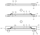
도 1은 실시 예에 따른 패키지 온 패키지 타입 적층 패키지를 도시한 단면도이다.
도 2는 실시 예에 따른 패키지 온 패키지 타입 적층 패키지에서 제1봉지부재가 부분 절개된 상태의 바텀 패키지를 도시한 평면도이다.
도 3은 실시 예에 따른 패키지 온 패키지 타입 적층 패키지의 효과를 설명하기 위한 종래의 패키지 온 패키지 타입 적층 패키지를 도시한 단면도이다.
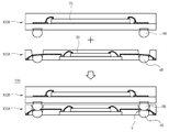
도 4는 실시 예에 따른 패키지 온 패키지 타입 적층 패키지에서의 바텀 패키지의 제조방법을 설명하기 위한 단면도이다.
도 5는 실시 예에 따른 패키지 온 패키지 타입 적층 패키지에서의 탑 패키지의 제조방법을 설명하기 위한 단면도이다.
도 6은 실시 예에 따른 패키지 온 패키지 타입 적층 패키지의 제조방법을 설명하기 위한 단면도이다.
도 7은 실시 예에 따른 패키지 온 패키지 타입 적층 패키지를 적용한 전자 시스템의 블록도이다.
도 8은 실시 예에 따른 패키지 온 패키지 타입 적층 패키지를 포함하는 메모리 카드의 블록도이다.1 is a cross-sectional view illustrating a package-on-a-package type stacked package according to an embodiment.
2 is a plan view showing a bottom package in a state in which the first sealing member is partially cut in the package-on-package type laminate package according to the embodiment.
3 is a cross-sectional view illustrating a conventional package-on-a-package type stacked package for explaining the effect of the package-on-package type stacked package according to the embodiment.
4 is a cross-sectional view illustrating a method of manufacturing a bottom package in a package-on-package type laminate package according to an embodiment.
5 is a cross-sectional view illustrating a method of manufacturing a top package in a package-on-package type stacked package according to an embodiment.
6 is a cross-sectional view illustrating a method of manufacturing a package-on-a-package type stacked package according to an embodiment.
7 is a block diagram of an electronic system applying a package-on-package type stack package according to an embodiment.
8 is a block diagram of a memory card including a package on package type stacked package according to an embodiment.
본 발명의 실시 예는 여러 가지 형태로 변형될 수 있으며, 본 발명의 범위가 아래에서 상세히 설명하는 실시 예로 한정되는 것으로 해석되어서는 안 된다. 즉, 본 발명의 실시 예는 당업계에서 평균적인 지식을 가진 자에게 본 발명을 더욱 상세하게 설명하기 위해서 제공되는 것이다. 따라서, 도면에서의 구성요소의 형상 등은 보다 명확한 설명을 강조하기 위해서 과장되어 표현될 수 있으며, 각 도면에서 동일한 부재는 동일한 참조부호로 도시하였음을 유의하여야 한다. The embodiments of the present invention can be modified in various forms, and the scope of the present invention should not be construed as being limited to the embodiments described in detail below. In other words, the embodiments of the present invention are provided to explain the present invention to the average person skilled in the art in more detail. Accordingly, it should be noted that the shapes and the like of the components in the drawings may be exaggerated in order to emphasize a clearer description, and the same members are denoted by the same reference numerals in the drawings.
이하, 첨부된 도면들을 참조하여 다양한 실시 예들을 상세하게 설명하도록 한다.Various embodiments will now be described in detail with reference to the accompanying drawings.
도 1을 참조하면, 실시 예에 따른 패키지 온 패키지 타입 적층 패키지(100)는 바텀 패키지(100A) 및 상기 바텀 패키지(100A) 상에 적층된 탑 패키지(100B)를 포함할 수 있다. Referring to FIG. 1, a package-on-package
실시 예에서, 바텀 패키지(100A)는 기판 없이 구성될 수 있으며, 제1본드핑거들(12), 인터포저(20), 제1반도체칩(30), 본딩와이어들(42, 44), 제1봉지부재(46) 및 제1접속부재들(48)을 포함할 수 있다. 또한, 바텀 패키지(100A)는 인터포저(20)와 제1반도체칩(30) 사이에 개재된 제1접착부재(40)를 더 포함할 수 있다.In an embodiment, the
상기 제1본드핑거들(12)은 금속과 같은 도전성 물질의 패턴으로 이루어질 수 있으며, 인터포저(20)의 가장자리로부터 소정 간격 이격해서 복수 개가 배열될 수 있다. 예를 들어, 도 2에서와 같이 인터포저(20)가 사각 플레이트 형상을 가질 때, 제1본드핑거들(12)은 인터포저(20)를 네 가장자리를 둘러싸는 형태로 일정 간격으로 배열될 수 있다. 이와 다르게, 도시되지 않았으나 제1본드핑거들(12)은 인터포저(20)의 양측 가장자리에만 복수 개가 배열되도록 마련되는 것도 가능하다. The
여기서, 제1본드핑거들(12)은 제2본딩와이어(44)가 연결될 수 있는 크기를 가질 수 있으며, 또한, 제1봉지부재(46)에 제2본딩와이어들(44)의 일부분들을 각각 노출시키는 비아홀들(v)이 충분히 형성될 수 있는 간격으로 인터포저(20)의 네 가장자리로부터 이격해서 배열될 수 있다. Herein, the
상기 인터포저(20)는 제1본드핑거들(12)과 제1반도체칩(30) 사이의 연결 매개체로서, 대체로 사각 플레이트 형상을 가질 수 있다. 이러한 사각 플레이트 형상의 인터포저(20)는 상면(20a) 및 하면(20b)을 가지며, 적어도 제1본드핑거들(12)에 대응하는 수만큼 상면(20a)의 네 가장자리를 따라 배열되는 복수의 전극들(22)을 포함할 수 있다. 전극들(22)은 인터포저(20)의 상면(20a) 상에 배치될 수 있으며, 이와 다르게, 전극들(22)은 인터포저(20)에 매립되어 그의 일면이 인터포저(20)의 상면(20a)으로 노출된 형상으로 배치될 수도 있다. 전극들(22)은 제1반도체칩(30)에 인접하여 배치되는 일단(22-1) 및 상기 일단(22-1)으로부터 인터포저(20)의 가장자리를 향해 연장된 타단(22-2)을 포함할 수 있다. The
상기 제1반도체칩(30)은 로직 칩(logic chip) 일 수 있으며, 이와 다르게, 제1반도체칩(30)은 메모리 칩 일 수 있다. 제1반도체칩(30)은 상면(30a) 및 상면(30a)에 대향하는 하면(30b)을 갖는 사각 플레이트 형상으로 마련될 수 있다. 제1반도체칩(30)은 상면(30a)의 네 가장자리를 따라 배열되는 복수의 제1본딩패드들(32)을 포함할 수 있다. 이와 다르게, 전극들(22)이 인터포저(20)의 상면(20a) 양측 가장자리에만 배열될 경우, 제1본딩패드들(32)은 전극들(22)에 인접하는 제1반도체칩(30)의 상면(30a) 양측 가장자리에만 배열될 수 있다. 이러한 제1반도체칩(30)은 그의 하면(30b)이 인터포저(20)의 상면(20a)과 접하고 전극들(22)을 노출하도록 인터포저(20)의 상면(20a) 중앙부에 페이스-업 타입(face-up)으로 배치될 수 있다. 이때, 제1반도체칩(30)은 제1접착부재(40)를 매개로 하여 인터포저(20)의 상면(20a) 중앙부에 고정될 수 있다.The
상기 제1본딩와이어들(42)은 와이어 본딩 공정을 통해 제1반도체칩(30)의 제1본딩패드들(32)과 이에 인접하여 배열된 인터포저(20) 전극들(22)의 일단들(22-1)을 상호 연결하도록 형성될 수 있다. 상기 제2본딩와이어들(44)은 와이어 본딩 공정을 통해 일단(22-1)에 제1본딩와이어들(42)이 연결된 인터포저(20) 전극들(22)의 타단들(22-2)과 이에 대응하여 배열된 제1본드핑거들(12)을 상호 연결하도록 형성될 수 있다. The
상기 제1봉지부재(46)는 제1반도체칩(30)을 외부 영향으로부터 보호하기 위해 마련되는 것으로, 예를 들어, EMC(Epoxy Molding Compond)로 이루어질 수 있다. 이러한 제1봉지부재(46)는 제1본드핑거들(12)과 인터포저(20) 및 제1반도체칩(30)의 상면들 및 측면들과 제1 및 제2 본딩와이어들(42, 44)을 덮도록 형성될 수 있다. 또한, 제1봉지부재(46)는 제2본딩와이어들(44)의 일부분들을 각각 노출시키도록 형성된 복수 개의 TMV(Through Mold Via)들, 즉, 비아홀들(v)을 포함할 수 있다. The
본 실시 예에서, 비아홀들(v)은 도 1에서와 같이 하부 직경이 상부 직경 보다 작은 형태로 형성될 수 있으며, 이는 솔더 볼로 이루어지는 제1접속부재들(48)이 상기 비아홀들(v) 내에 안정적으로 삽입 설치되도록 하기 위함인 것으로 이해될 수 있다. 이와 다르게, 도시하지 않았으나 비아홀들(v)은 하부 및 상부가 동일 직경을 갖도록 형성될 수도 있다. 또한, 비아홀들(v)은 도 2에서와 같이 지그재그 형태로 배열되게 형성될 수 있다. 1, the via holes v may be formed in a shape such that the lower diameter is smaller than the upper diameter, because the first connecting
상기 제1접속부재들(48)은 탑 패키지(100B) 및 외부 회로와의 전기적 연결을 위해 마련되는 것으로, 예를 들어, 솔더 볼로 이루어질 수 있다. 솔더 볼로 이루어진 제1접속부재들(48)은 비아홀들(v) 내에 각각 삽입되어 각 비아홀들(v) 내에서 제2본딩와이어들(44)의 노출 부분들과 전기적으로 연결될 수 있다. 이때, 제1접속부재들(48)을 구성하는 솔더 볼은, 예를 들어 비아홀(v)의 상부 직경 보다 작고 하부 직경 보다 큰 직경을 갖도록 마련될 수 있으며, 이에 따라, 솔더 볼로 이루어진 제1접속부재들(48)은 각 비아홀들(v) 내의 아랫부분에 위치하게 되고, 특히, 외부 회로에의 접속이 용이하도록 일부분이 비아홀들(v)의 아래쪽으로, 즉, 바텀 패키지(100A)의 하부면 아래로 돌출하게 된다. The first connecting
한편, 전술한 실시 예에서는 제1본드핑거들(12), 전극들(22) 및 제1본딩패드들(32)가 네 가장자리를 따라 배열되는 경우를 도시하고 설명하였으나, 이와 다르게, 제1본드핑거들(12), 전극들(22) 및 제1본딩패드들(32)은 양측 가장자리에만 배열되도록 형성되는 것도 가능하다. In the above embodiment, the
계속해서, 본 실시 예에서의 탑 패키지(100B)는 기판(50), 제2반도체칩(70), 제3본딩와이어들(82), 제2봉지부재(86) 및 제2접속부재들(88)을 포함할 수 있다. 또한, 탑 패키지(100B)는 기판(50)과 제2반도체칩(70) 사이에 개재된 제2접착부재(60)를 더 포함할 수 있다.Subsequently, the
상기 기판(50)은 인쇄회로기판(Printed Circuit Board)일 수 있으며, 대체로 사각 플레이트 형상을 갖는다. 이러한 기판(50)은 상면(50a) 및 상면(50a)에 대향하는 하면(50b)을 가지며, 또한, 상면(50a) 가장자리에 배열된 복수의 제2본드핑거들(52) 및 하면(50b)에 배열된 복수의 외부전극들(54)을 포함할 수 있다. 제2본드핑거들(52)과 외부전극들(54)은 기판(50) 내부에 형성되는 비아 패턴들(도시안됨)에 의해 상호 전기적으로 연결될 수 있다. 여기서, 제2본드핑거들(52)은 기판(50)의 상면(50a) 가장자리를 따라 배열되되, 기판(50)이 사각 플레이트 형상을 가질 때, 제2본드핑거들(52)은 기판(50)의 양측 가장자리를 따라 배열될 수 있고, 이와 다르게, 네 가장자리들을 따라 배열될 수 있다.The
상기 제2반도체칩(70)은 상면(70a) 및 상면(70a)에 대향하는 하면(70b)을 갖는 사각 플레이트 형상으로 마련될 수 있다. 제2반도체칩(70)은 제2접착부재(60)를 매개로 하여 기판(50)의 상면(50a) 상에 부착될 수 있다. 이때, 제2반도체칩(70)은 그의 하면(70b)이 기판(50)의 상면(50a)과 마주하도록 배치되며, 특히, 제2본드핑거들(52)이 노출되도록 기판(50)의 상면(50a) 중앙부에 배치될 수 있다. The
본 실시 예에서, 제2반도체칩(70)은 메모리칩 일 수 있으며, 이와 다르게, 제2반도체칩(70)은 로직 칩 일 수 있다. In this embodiment, the
제2반도체칩(70)은 그의 상면(70a) 가장자리에 배열된 복수의 제2본딩패드들(72)을 포함할 수 있다. 제2본딩패드들(72)은 적어도 제2본드핑거들(52)에 대응하는 수만큼 배열될 수 있으며, 제2본드핑거들(52)과 마찬가지로 제2반도체칩(70)의 상면(70a)에 그의 양측 가장자리를 따라 배열될 수 있음은 물론, 네 가장자리들을 따라 배열될 수 있다. The
상기 제3본딩와이어들(82)은 와이어 본딩 공정을 통해 상호 대응하는 기판(50)의 제2본드핑거들(52)과 제2반도체칩(70)의 제2본딩패드들(72)을 연결하도록 형성될 수 있다. The
상기 제2봉지부재(86)는 제2반도체칩(70)을 외부 영향으로부터 보호하기 위한 것으로, 예를 들어 EMC로 이루어질 수 있다. 이러한 제2봉지부재(86)는 제2반도체칩(70) 및 제3본딩와이어들(82)을 덮도록 기판(50)의 상면(50a) 상에 형성될 수 있다. The
상기 제2접속부재들(88)은 기판(50)의 하면(50b)에 배열된 외부전극들(54) 상에 형성될 수 있다. 이러한 제2접속부재들(88)은 솔더 볼로 이루어지질 수 있으며, 바텀 패키지(100A)와의 적층 구조에서 바텀 패키지(100A)의 비아홀들(v) 내에 각각 삽입되어 솔더 볼로 이루어진 제1접속부재들(48)과 전기적으로 연결될 수 있다. 이때, 제2접속부재들(88)을 구성하는 솔더 볼들은 바텀 패키지(100A)의 비아홀들(v) 내에 삽입될 수 있도록 상기 비아홀들(v)의 상부 직경 보다 작은 직경을 갖도록 마련됨이 바람직하다. 본 실시 예에서, 솔더 볼들로 이루어지는 제2접속부재들(88)은 그 직경을 조절함에 따라 바텀 패키지(100A)와 탑 패키지(100B) 사이의 간격을 조절할 수 있고, 결과적으로, 실시 예에 따른 적층 패키지(100)의 전체 두께를 조절할 수 있다. The second connecting
이와 다르게, 제2접속부재들(88)은 솔더 페이스트로 이루어질 수 있으며, 이 경우에도 솔더 페이스트로 이루어지는 제2접속부재들(88)은 바텀 패키지(100A)의 비아홀들(v) 내에 각각 삽입되어 제1접속부재들(48)과 전기적으로 연결될 수 있다. Alternatively, the second connecting
한편, 본 실시 예에서는 상기와 같은 구조를 갖는 탑 패키지(100B)의 예를 도시하고 설명하였으나, 실시 예에 따른 적층 패키지(100)에서의 탑 패키지(100B)는 그 이외에도 다양한 구조의 것이 적용될 수 있다. 예를 들어, 탑 패키지(100B)는 반도체 칩 위에 범프를 형성하여 기판에 플립 칩 본딩으로 실장한 플립 칩 패키지일 수도 있다. In the meantime, although the example of the
전술한 바와 같은 구성을 갖는 본 실시 예에서의 바텀 패키지(100A)와 탑 패키지(100B)는 상기 탑 패키지(100B)의 제2접속부재들(88)이 바텀 패키지(100A)의 비아홀들(v) 내에 삽입되어 제1접속부재들(48)과 전기적으로 연결되는 것에 의해 패키지 온 패키지 타입 적층 패키지(100)를 구성하게 된다.The
따라서, 실시 예에 따른 패키지 온 패키지 타입 적층 패키지(100)는 바텀 패키지(100A)가 기판 없이 구성되는 것으로 인해 로우 프로파일(low profile)을 가지게 되고, 또한, 탑 패키지(100B)의 제2접속부재들(88)이 바텀 패키지(100A)의 비아홀들(v) 내에 삽입되는 것에 의해 전체 두께가 더욱 낮아지게 되며, 결과적으로, 얇은 프로파일(low profile)을 갖게 된다. Thus, the package-on-package
구체적으로, 도 3에 도시된 바와 같이, 종래의 패키지 온 패키지 타입 적층 패키지(200)는 바텀 패키지(200A)가 기판(110)을 포함하고, 탑 패키지(200B)의 제2접속부재들(188)이 바텀 패키지(200A)에서의 기판(110)의 상면에 마련된 볼랜드들(112)과 콘택하는 구조를 갖는다.3, the conventional package-on-package
반면, 도 1에 도시된 바와 같이, 실시 예에 따른 패키지 온 패키지 타입 적층 패키지(100)는 바텀 패키지(100A)가 기판 없이 구성되는 것에 의해 로우 프로파일을 갖고, 또한, 탑 패키지(100B)의 제2접속부재들(88)이 바텀 패키지(100A)의 비아홀들(v) 내에 삽입 배치되는 구조를 갖는다. On the other hand, as shown in FIG. 1, the package-on-package
그러므로, 실시 예에 따른 패키지 온 패키지 타입 적층 패키지(100)는 종래의 패키지 온 패키지 타입 적층 패키지(200)와 비교해서 전체 두께가 감소되어 얇은 프로파일을 갖는다. Therefore, the package-on-package
이하에서는 실시 예에 따른 바텀 패키지 및 탑 패키지의 제조방법과 패키지 온 패키지 타입 적층 패키지의 제조방법을 설명하도록 한다.Hereinafter, a method of manufacturing a bottom package and a top package according to an embodiment, and a method of manufacturing a package-on-package type stacked package will be described.
먼저, 바텀 패키지(100A)는 다음과 같은 순서로 제조될 수 있다. First, the
도 4를 참조하면, 임시 기판(10)을 마련한다. 여기서, 임시 기판(10)으로서 케리어 테이프 또는 마운트 테이프를 적용할 수 있다. 임시 기판(10)의 상면(10a) 상에, 예를 들어, 도전막 형성 공정과, 형성된 도전막에 대한 식각 공정을 차례로 진행하여 복수의 제1본드핑거들(12)을 형성한다. 여기서, 제1본드핑거들(12)은 후속에서 임시 기판(10)의 상면(10a) 상에 배치되는 사각 플레이트 형상을 갖는 인터포저(20)의 네 가장자리들을 둘러싸는 형태로 배열되도록 형성한다. Referring to FIG. 4, a
임시 기판(10)의 상면(10a) 상에 대체로 사각 플레이트 형상을 갖는 인터포저(20)를 부착한다. 인터포저(20)는 상면(20a) 및 상면(20a)에 대향하는 하면을 갖고, 상면(20a) 가장자리를 따라 배열된 복수의 전극들(22)을 포함할 수 있다. 이러한 인터포저(20)는 그의 하면(20b)이 임시 기판(10)과 마주하고 제1본드핑거들(12)을 노출하도록 배치될 수 있다. 전극들(22)은 일단(22-1) 및 타단(22-2)을 포함할 수 있다. 인터포저(20)의 상면(20a) 상에 대체로 사각 플레이트 형상을 갖는 제1반도체칩(30)을 부착한다. 전술한 바와 같이, 제1반도체칩(30)은 로직 칩일 수 있으며, 상면(30a) 및 상면(30a)에 대향하는 하면(30b)을 갖고, 그의 상면(30a) 가장자리를 따라 배열된 복수의 제1본딩패드들(32)을 포함할 수 있다. 이러한 제1반도체칩(30)은 전극들(22)을 노출하도록 인터포저(20)의 상면(20a) 중앙부 상에 제1접착부재(40)을 매개로 하여 페이스-업 타입으로 부착될 수 있다. 제1반도체칩(30)은 메모리칩 일 수도 있다. An
와이어 본딩 공정을 통해, 상호 인접하여 배열된 제1반도체칩(30)의 제1본딩패드들(32)과 인터포저(20) 전극들(22)의 일단들(22-1)을 연결하는 제1본딩와이어들(42)을 형성하고, 그리고, 상호 인접하여 배열된 인터포저(20) 전극들(22)의 타단들(22-2)과 제1본드핑거들(12)을 연결하는 제2본딩와이어들(44)을 형성한다. (22-1) of interposer (20) electrodes (22) through first bonding pads (32) of a first semiconductor chip (30) arranged adjacent to each other through a wire bonding process 1
여기서, 제1 및 제2 본딩와이어들(42, 44)을 형성하기 위한 와이어 본딩 공정은 제1본딩와이어들(42)을 우선 형성한 후, 이어서 제2본딩와이어들(44)을 형성하는 방식으로 진행하거나, 이와는 반대로 제2본딩와이어들(44)을 우선 형성한 후, 이어서 제1본딩와이어들(42)을 형성하는 방식으로 진행할 수 있다. 또한, 와이어 본딩 공정은 하나의 제1본드핑거(12)와 전극(22) 및 제1본딩패드(32)에 대하여 제1본딩와이어(42)와 제2본딩와이어(44)를 차례로 형성한 후, 이와 같은 방식으로 나머지 제1본드핑거들(12)과 전극들(22) 및 제1본딩패드들(32)에 대해서 연속으로 제1본딩와이어(42)와 제2본딩와이어(44)를 차례로 형성하는 방식으로 진행하는 것도 가능하다. The wire bonding process for forming the first and
제1반도체칩(30)과 제1 및 제2 본딩와이어들(42, 44)을 덮도록 임시 기판(10)의 상면(10a) 상에 제1봉지부재(46)를 형성한다. 제1봉지부재(46)는, 예를 들어, EMC(Epoxy Molding Compound)일 수 있다. 이때, 제1봉지부재(46)는 바텀 패키지(100A)의 두께를 고려하여 최소 두께를 갖도록 형성함이 바람직하다. 제1봉지부재(46)에 제2본딩와이어들(44)의 일부분을 각각 노출하는 TMV들, 즉, 비아홀들(v)을 형성한다. 비아홀들(v)의 형성은 레이저 드릴링 공정, 또는, 포토 및 식각 공정들로 진행할 수 있다. The
제1봉지부재(46) 및 비아홀들(v)이 형성된 결과물로부터 임시 기판(10)을 제거한다. 그런 다음, 각 비아홀들(v) 내에 각각 구형의 솔더 볼들을 삽입한 후, 이에 대한 리플로우(reflow)를 실시하여 각 비아홀들(v) 내에 삽입 배치되면서 상기 비아홀들(v)에 의해 노출된 제2본딩와이어들(44) 부분들과 전기적으로 연결되는 솔더 볼들로 이루어진 제1접속부재들(48)을 형성하고, 이 결과로서, 바텀 패키지(100A)의 제조를 완성한다. The
여기서, 상기 제1접속부재들(48)을 구성하는 솔더 볼들은 각 비아홀들(v) 내에서 아랫부분에 위치하게 되며, 특히, 그의 일부분이 바텀 패키지(100A)의 하부면으로 돌출하게 된다. Here, the solder balls constituting the first connecting
한편, 본 실시 예에서는 임시 기판(10)의 제거 후에 솔더 볼로 이루어진 제1접속부재들(48)을 형성하는 방식을 적용하였지만, 이와 반대로, 제1접속부재들(48)을 형성한 후에 임시 기판(10)을 제거하는 방식을 적용하는 것도 가능하다. Meanwhile, in this embodiment, the first connecting
다음으로, 탑 패키지(100B)는 다음과 같은 순서로 제조될 수 있다. Next, the
도 5를 참조하면, 상면(50a)에 제2본드핑거들(52)이 배열되고 하면(50b)에 외부전극들(54)이 배열된 기판(50)을 마련한다. 전술한 바와 같이 기판(50)은 인쇄회로기판일 수 있으며, 대체로 사각 플레이트 형상을 가질 수 있다. 제2본드핑거들(52)은 기판(50) 상면(50a)의 양측 가장자리는 물론 네 가장자리들을 따라 복수 개가 배열될 수 있다. 5, the
기판(50)의 상면(50a) 상에 제2접착부재(60)를 매개로 하여 제2반도체칩(70)을 부착한다. 제2반도체칩(70)은 메모리칩 일 수 있으며, 기판(50)보다 작은 크기를 가지면서 대체로 사각 플레이트 형상을 가질 수 있다. 제2반도체칩(70)은 그의 상면(70a) 가장자리에 배열된 복수 개의 제2본딩패드들(72)을 포함하며, 그의 하면(70b)이 기판(50)의 상면(50a)와 마주하도록 페이스-업 타입으로 배치될 수 있고, 특히, 제2본드핑거들(52)이 노출되도록 배치될 수 있다. 제2반도체칩(70)은 로직 칩 일 수도 있다. 와이어 본딩 공정을 통해 상호 인접하여 배치된 제2반도체칩(70)의 제2본딩패드들(72)과 기판(50)의 제2본드핑거들(52)을 연결하는 제3본딩와이어들(82)을 형성한다. The
제2반도체칩(70) 및 제3본딩와이어들(82)을 덮도록 기판(50)의 상면(50a) 상에 제2봉지부재(86)를 형성한다. 제2봉지부재(86)는, 예를 들어, EMC로 형성할 수 있다. 기판(50)의 하면(50b)에 배열된 외부전극들(54) 각각에, 예를 들어, 솔더 볼로 이루어진 제2접속부재들(88)을 형성하고, 이를 통해, 탑 패키지(100B)의 제조를 완성한다. 여기서, 솔더 볼로 이루어진 제2접속부재들(88)의 형성은, 예를 들어, 외부전극들(54) 상에 각각 솔더 볼을 도팅한 후, 이들을 리플로우(reflow)하는 것에 의해 달성될 수 있다. The
도 6을 참조하면, 전술한 바와 같은 제조 공정들을 통해 바텀 패키지(100A)와 탑 패키지(100B)를 마련한 후, 바텀 패키지(100A) 상부에 제1접속부재들(48)과 제2접속부재들(88)이 상호 연결되도록 탑 패키지(100B)를 적층 함으로써 실시 예에 따른 패키지 온 패키지 타입 적층 패키지(100)를 제조할 수 있다. Referring to FIG. 6, after the
여기서, 탑 패키지(100B)의 적층은 솔더 볼로 이루어진 제2접속부재들(88)이 바텀 패키지(100A)의 비아홀들(v) 내에 삽입되고, 그리고, 비아홀들(v) 내에서 바텀 패키지(100A)의 솔더 볼로 이루어진 제1접속부재들(48)과 전기적 및 물리적으로 연결되는 것에 의해 이루어질 수 있다. Here, the stacking of the
상술한 패키지 온 패키지 타입 적층 패키지는 다양한 종류의 반도체 장치들 및 이를 구비하는 패키지 모듈에 적용될 수 있다. The package-on-package type stacked package described above can be applied to various types of semiconductor devices and a package module having the same.
도 9는 실시 예들에 따른 패키지 온 패키지 타입 적층 패키지를 적용한 전자 시스템의 블록도이다. 도시된 바와 같이, 전자 시스템(1000)은 콘트롤러(1100), 입출력장치(1200) 및 메모리장치(1300)를 포함할 수 있다. 콘트롤러(1100), 입출력장치(1200) 및 메모리장치(1300)는 데이터들이 이동하는 통로를 제공하는 버스(1500)를 통하여 결합될 수 있다. 9 is a block diagram of an electronic system employing a package-on-package type stack package according to embodiments. As shown, the
예컨대, 콘트롤러(1100)는 적어도 하나의 마이크로프로세서, 디지털신호프로세서, 마이크로컨트롤러, 그리고 이들과 유사한 기능을 수행할 수 있는 논리소자들 중에서 적어도 어느 하나를 포함할 수 있다. 콘트롤러(1100) 및 메모리장치(1300)는 실시 예에 따른 적층 패키지를 포함할 수 있다. 입출력장치(1200)는 키패드, 키보드 및 표시 장치 등에서 선택된 적어도 하나를 포함할 수 있다. For example, the
메모리장치(1300)는 데이터 및/또는 콘트롤러(1100)에 의해 실행되는 명령어 등을 저장할 수 있다. 메모리장치(1300)는 디램과 같은 휘발성 메모리 소자 및/또는 플래시 메모리와 같은 비휘발성 메모리 소자를 포함할 수 있다. 예컨대, 모바일 기기나 데스크 톱 컴퓨터와 같은 정보 처리 시스템에 플래시 메모리가 장착될 수 있다. 이러한 플래시 메모리는 반도체 디스크 장치(SSD)로 구성될 수 있다. 이 경우 전자 시스템(1000)은 대용량의 데이터를 플래시 메모리 시스템에 안정적으로 저장할 수 있다.The
이와 같은 전자 시스템(1000)은 통신 네트워크로 데이터를 전송하거나 통신 네트워크로부터 데이터를 수신하기 위한 인터페이스(1400)를 더 포함할 수 있다. 인터페이스(1400)는 유무선 형태일 수 있다. 예컨대, 인터페이스(1400)는 안테나 또는 유무선 트랜시버 등을 포함할 수 있다. Such an
한편, 도시하지 않았으나, 전자 시스템(1000)은 응용 칩셋(Application Chipset) 및 카메라 이미지 프로세서 등을 더 포함할 수 있다.Meanwhile, although not shown, the
전자 시스템(1000)은 모바일 시스템, 개인용 컴퓨터, 산업용 컴퓨터 또는 다양한 기능을 수행하는 로직 시스템 등으로 구현될 수 있다. 예컨대, 모바일 시스템은 개인 휴대용 정보 단말기(PDA; Personal Digital Assistant), 휴대용 컴퓨터, 웹 타블렛(web tablet), 모바일폰(mobile phone), 스마트폰(smart phone), 무선폰(wireless phone), 랩톱(laptop) 컴퓨터, 메모리 카드, 디지털 뮤직 시스템 (digital music system), 그리고, 정보 전송/수신 시스템 중 어느 하나일 수 있다.The
전자 시스템(1000)이 무선 통신을 수행할 수 있는 장비인 경우에, 전자 시스템(1000)은 CDMA(Code Division Multiple Access), GSM(Global System for Mobile communication), NADC(North American Digital Cellular), E-TDMA(Enhanced-Time Division Multiple Access), WCDMA(Wideband Code Division Multiple Access), CDMA2000, LTE(Long Term Evolution), Wibro(Wireless Broadband Internet)과 같은 통신 시스템에서 사용될 수 있다.In the case where the
도 10은 실시 예에 따른 패키지 온 패키지 타입 적층 패키지를 포함하는 메모리 카드의 블록도이다. 도시된 바와 같이, 실시 예에 따른 적층 패키지는 메모리 카드(2000)의 형태로 제공될 수 있다. 일례로, 메모리 카드(2000)는 비휘발성 메모리 소자와 같은 메모리(2100) 및 메모리 콘트롤러(2200)를 포함할 수 있다. 메모리(2100) 및 메모리 콘트롤러(2200)는 데이터를 저장하거나 저장된 데이터를 판독할 수 있다.10 is a block diagram of a memory card including a package-on-a-package type stack package according to an embodiment. As shown, the stacked package according to the embodiment may be provided in the form of a
메모리(2100)는 전술한 실시 예에 따른 적층 패키지가 적용된 비휘발성 메모리 소자들 중에서 적어도 어느 하나를 포함할 수 있다. 메모리 콘트롤러(2200)는 호스트(2300)의 판독/쓰기 요청에 응답하여 저장된 데이터를 독출하거나, 데이터를 저장하도록 메모리(2100)를 제어할 수 있다.The
이상, 여기에서는 본 발명을 특정 실시예에 관련하여 도시하고 설명하였지만, 본 발명이 그에 한정되는 것은 아니며, 이하의 특허청구의 범위는 본 발명의 정신과 분야를 이탈하지 않는 한도 내에서 본 발명이 다양하게 개조 및 변형될 수 있다는 것을 당업계에서 통상의 지식을 가진 자가 용이하게 알 수 있다. While the present invention has been particularly shown and described with reference to specific embodiments thereof, it is to be understood that the invention is not limited to the disclosed embodiments, but, on the contrary, It will be readily apparent to those skilled in the art that the present invention can be modified and changed without departing from the scope of the present invention.
10: 임시 기판 12: 제1본드핑거
20: 인터포저 22: 전극
30: 제1반도체칩 32: 제1본딩패드
40: 제1접착부재 42: 제1본딩와이어
44: 제2본딩와이어 46: 제1봉지부재
48: 제1접속부재 50: 기판
52: 제2본드핑거 54: 외부전극
60: 제2접착부재 70: 제2반도체칩
72: 제2본딩패드 82: 제3본딩와이어
86: 제2봉지부재 88: 제2접속부재
100: 적층 패키지 100A: 바텀 패키지
100B: 탑 패키지10: temporary substrate 12: first bond finger
20: interposer 22: electrode
30: first semiconductor chip 32: first bonding pad
40: first bonding member 42: first bonding wire
44: second bonding wire 46: first sealing member
48: first connecting member 50: substrate
52: second bond finger 54: external electrode
60: second bonding member 70: second semiconductor chip
72: second bonding pad 82: third bonding wire
86: second sealing member 88: second connecting member
100:
100B: Top package
Claims (19)
상기 바텀 패키지의 상부에 배치되며, 제2반도체칩 및 상기 제1접속부재들과 전기적으로 연결된 제2접속부재들을 갖는 탑 패키지;
를 포함하며,
상기 바텀 패키지는,
상면 가장자리에 배열된 복수의 전극들을 갖는 인터포저;
상기 인터포저의 가장자리로부터 이격하여 배열된 복수의 제1본드핑거들;
상기 인터포저의 상면 상에 상기 전극들을 노출하도록 배치되며, 상면에 배열된 복수의 제1본딩패드들을 갖는 제1반도체칩;
상기 제1본딩패드들과 상기 전극들을 연결하는 제1본딩와이어들;
상기 전극들과 상기 제1본드핑거들을 연결하는 제2본딩와이어들; 및
상기 제1본드핑거들, 인터포저 및 제1반도체칩의 상면 및 측면과 상기 제1 및 제2 본딩와이어들을 덮도록 형성되며, 상기 제2본딩와이어들의 일부분들을 각각 노출하는 비아홀들을 갖는 제1봉지부재;
를 포함하는 적층 패키지. A bottom package having a first semiconductor chip and first connecting members; And
A top package disposed on top of the bottom package, the top package having a second semiconductor chip and second connecting members electrically connected to the first connecting members;
/ RTI >
Wherein the bottom package comprises:
An interposer having a plurality of electrodes arranged at an upper surface edge;
A plurality of first bond fingers spaced apart from an edge of the interposer;
A first semiconductor chip disposed on the upper surface of the interposer to expose the electrodes, the first semiconductor chip having a plurality of first bonding pads arranged on an upper surface thereof;
First bonding wires connecting the first bonding pads and the electrodes;
Second bonding wires connecting the electrodes and the first bond fingers; And
The first bonding fingers, the first bonding fingers, the interposer, and the first semiconductor chip, and the first bonding wires and the second bonding wires, A sealing member;
≪ / RTI >
상기 제1반도체칩은 로직 칩을 포함하고, 상기 제2반도체칩은 메모리 칩을 포함하는 것을 특징으로 하는 적층 패키지. The method according to claim 1,
Wherein the first semiconductor chip comprises a logic chip and the second semiconductor chip comprises a memory chip.
상기 인터포저 및 상기 제1반도체칩이 사각 플레이트 형상을 가질 때, 상기 제1본드핑거들은 상기 인터포저의 네 가장자리들을 둘러싸는 형태로 배열되고, 상기 전극들 및 제1본딩패드들은 상기 인터포저 및 상기 제1반도체칩의 상면들의 네 가장자리들을 따라 배열된 것을 특징으로 하는 적층 패키지. The method according to claim 1,
When the interposer and the first semiconductor chip have a rectangular plate shape, the first bond fingers are arranged to surround the four edges of the interposer, and the electrodes and the first bonding pads are connected to the interposer Wherein the second semiconductor chip is arranged along four edges of the upper surfaces of the first semiconductor chip.
상기 비아홀들은 하부 직경이 상부 직경 보다 작은 형태를 갖는 것을 특징으로 하는 적층 패키지. The method according to claim 1,
Wherein the via holes have a shape in which the lower diameter is smaller than the upper diameter.
상기 제1접속부재들은 상기 비아홀들 내에 각각 삽입되어 상기 제2본딩와이어들의 노출 부분들과 연결되는 것을 특징으로 하는 적층 패키지. The method according to claim 1,
And the first connecting members are respectively inserted into the via holes and connected to the exposed portions of the second bonding wires.
상기 제1접속부재들은 솔더 볼을 포함하는 것을 특징으로 하는 적층 패키지.The method according to claim 1,
And the first connecting members include solder balls.
상기 솔더 볼들은 상기 비아홀들의 상부 직경 보다 작고 하부 직경 보다 큰 직경을 갖는 것을 특징으로 하는 적층 패키지.The method according to claim 6,
Wherein the solder balls have a diameter smaller than an upper diameter of the via holes and larger than a lower diameter of the via holes.
상기 솔더 볼들은 상기 비아홀들 내부에서 아랫부분에 위치하면서 바텀 패키지의 하부면으로 일부분이 돌출되도록 배치된 것을 특징으로 하는 적층 패키지.8. The method of claim 7,
Wherein the solder balls are disposed at a lower portion inside the via holes and partially protruded from a lower surface of the bottom package.
상기 제2접속부재들은 상기 바텀 패키지의 비아홀들 내에 각각 삽입되어 사기 제1접속부재들과 연결되는 것을 특징으로 하는 적층 패키지.The method according to claim 1,
And said second connecting members are respectively inserted into via holes of said bottom package and connected to said first connecting members.
상기 탑 패키지는,
상면 및 상기 상면에 대향하는 하면을 가지며, 상기 상면에 배열된 제2본드핑거들 및 상기 하면에 배열되고 상기 제2본드핑거들과 전기적으로 연결되며 상기 제2접속부재들과 연결되는 외부전극들을 포함하는 기판;
상기 제2본드핑거들이 노출되도록 상기 기판의 상면 상에 배치되며, 상면에 배열된 복수의 제2본딩패드들을 갖는 상기 제2반도체칩;
상기 제2본딩패드들과 상기 제2본드핑거들을 연결하는 제3본딩와이어들; 및
상기 제2반도체칩 및 제3본딩와이어들을 덮도록 상기 기판의 상면 상에 형성된 제2봉지부재;
를 포함하는 것을 특징으로 하는 적층 패키지. 10. The method of claim 9,
The top package includes:
Second electrodes arranged on the lower surface and electrically connected to the second bond fingers and having external electrodes connected to the second connection members, the external electrodes having an upper surface and a lower surface facing the upper surface, A substrate;
The second semiconductor chip being disposed on an upper surface of the substrate such that the second bond fingers are exposed, the second semiconductor chip having a plurality of second bonding pads arranged on an upper surface thereof;
Third bonding wires connecting the second bonding pads and the second bond fingers; And
A second sealing member formed on an upper surface of the substrate to cover the second semiconductor chip and the third bonding wires;
≪ / RTI >
상기 제2접속부재들은 솔더 볼 또는 솔더 페이스트를 포함하는 것을 특징으로 하는 적층 패키지. 10. The method of claim 9,
And the second connecting members comprise solder balls or solder paste.
상기 제1접속부재들과 제2접속부재들이 상호 연결되도록 상기 바텀 패키지의 상부에 탑 패키지를 적층하는 단계;
를 포함하며,
상기 바텀 패키지를 마련하는 단계는,
상면에 복수의 제1본드핑거들이 배열된 임시 기판을 마련하는 단계;
상기 제1본드핑거들이 노출되도록 상기 임시 기판의 상면 상에 상면에 복수의 전극들이 배열된 인터포저를 배치하는 단계;
상기 전극들이 노출되도록 상기 인터포저의 상면 상에 상면에 복수의 제1본딩패드들이 배열된 제1반도체칩을 배치하는 단계;
상기 제1본딩패드들과 전극들을 연결하는 제1본딩와이어들 및 상기 전극들과 제1본드핑거들을 연결하는 제2본딩와이어들이 형성하는 단계;
상기 제1 및 제2 본딩와이어들과 인터포저 및 제1반도체칩을 덮도록 상기 임시 기판의 상면 상에 제1봉지부재를 형성하는 단계;
상기 제1봉지부재 내에 상기 제2본딩와이어들의 일부분을 각각 노출하는 비아홀들을 형성하는 단계;
상기 임시 기판을 제거하는 단계; 및
상기 제2본딩와이어들과 연결되도록 각 비아홀들 내에 상기 제1접속부재들을 형성하는 단계;
를 포함하는 적층 패키지의 제조방법. Providing a bottom package having a first semiconductor chip and first connecting members and a top package having a second semiconductor chip and second connecting members; And
Stacking a top package on top of the bottom package such that the first connecting members and the second connecting members are interconnected;
/ RTI >
The step of providing the bottom package may include:
Providing a temporary substrate having a plurality of first bond fingers arranged on an upper surface thereof;
Disposing an interposer in which a plurality of electrodes are arranged on an upper surface of the temporary substrate so that the first bond fingers are exposed;
Disposing a first semiconductor chip having a plurality of first bonding pads arranged on an upper surface thereof on an upper surface of the interposer so that the electrodes are exposed;
Forming first bonding wires connecting the first bonding pads and the electrodes and second bonding wires connecting the electrodes and the first bond fingers;
Forming a first sealing member on the upper surface of the temporary substrate to cover the first and second bonding wires and the interposer and the first semiconductor chip;
Forming via holes that respectively expose a portion of the second bonding wires in the first sealing member;
Removing the temporary substrate; And
Forming the first connecting members in respective via holes to be connected to the second bonding wires;
≪ / RTI >
상기 제1반도체칩은 로직 칩을 포함하고, 상기 제2반도체칩은 메모리 칩을 포함하는 것을 특징으로 하는 적층 패키지의 제조방법. 13. The method of claim 12,
Wherein the first semiconductor chip comprises a logic chip and the second semiconductor chip comprises a memory chip.
상기 임시 기판, 인터포저 및 제1반도체칩이 사각 플레이트 형상을 가질 때, 상기 제1본드핑거들, 전극들 및 제1본딩패드들은 각각 상기 임시 기판, 인터포저 및 제1반도체칩의 상면 네 가장자리들을 따라 배열되도록 형성하는 것을 특징으로 하는 적층 패키지의 제조방법. 13. The method of claim 12,
When the temporary substrate, the interposer, and the first semiconductor chip have a rectangular plate shape, the first bond fingers, the electrodes, and the first bonding pads are formed on the upper surface of the temporary substrate, the interposer, Are formed in such a manner that they are arranged along the longitudinal direction.
상기 제1접속부재들은 솔더 볼을 포함하는 것을 특징으로 하는 적층 패키지의 제조방법. 13. The method of claim 12,
Wherein the first connecting members comprise solder balls.
상기 바텀 패키지 상부에 상기 탑 패키지를 적층하는 단계는, 상기 탑 패키지의 제2접속부재들이 상기 바텀 패키지의 비아홀들 내에 삽입되어 상기 제1접속부재들과 연결되도록 수행하는 것을 특징으로 하는 적층 패키지의 제조방법. 13. The method of claim 12,
Wherein the step of laminating the top package on top of the bottom package is performed so that the second connecting members of the top package are inserted into the via holes of the bottom package and connected to the first connecting members. Gt;
상기 제1본딩와이어들 및 제2본딩와이어들을 형성하는 단계는, 상기 제1본딩패드들과 전극들을 연결하는 제1본딩와이어들을 형성한 후에 상기 전극들과 제1본드핑거들을 연결하는 제2본딩와이어들을 형성하는 방식, 상기 제1본드핑거들과 전극들을 연결하는 제2본딩와이어들을 형성한 후에 상기 전극들과 제1본딩패드들을 연결하는 제2본딩와이어들을 형성하는 방식, 또는, 하나의 제1본드핑거와 전극 및 제1본딩패드를 연결하는 제1 및 제2 본딩와이어들을 형성한 후에 나머지 제1본드핑거들과 전극들 및 제1본딩패드들에 대해 연속으로 제1본딩와이어와 제2본딩와이어를 형성하는 방식 중에서 어느 하나로 수행하는 것을 특징으로 하는 적층 패키지의 제조방법.13. The method of claim 12,
The forming of the first bonding wires and the second bonding wires may include forming first bonding wires connecting the first bonding pads and the electrodes and then bonding the electrodes to the first bonding fingers, A method of forming second bonding wires connecting the electrodes and the first bonding pads after forming the second bonding wires connecting the first bond fingers and the electrodes, After forming the first and second bonding wires connecting the one-bond finger, the electrode, and the first bonding pad, the first bonding wire and the second bonding wire are continuously connected to the remaining first bond fingers and the electrodes and the first bonding pads, And the bonding wires are formed on the substrate.
상기 탑 패키지를 마련하는 단계는,
상면에 제2본드핑거들이 배열되고 하면에 외부전극들이 배열된 기판의 상기 상면 상에 상기 제2본드핑거들이 노출되도록 상면에 복수의 제2본딩패드들이 배열된 제1반도체칩을 부착하는 단계;
상기 제2본딩패드들과 제2본드핑거들을 연결하도록 제3본딩와이어들을 형성하는 단계;
상기 제2반도체칩 및 제3본딩와이어들을 덮도록 상기 기판의 상면 상에 제2봉지부재를 형성하는 단계; 및
상기 기판 하면의 외부전극들에 각각 제2접속부재들을 부착하는 단계;
를 포함하는 것을 특징으로 하는 적층 패키지의 제조방법. 13. The method of claim 12,
The step of providing the top package may include:
Attaching a first semiconductor chip on which a plurality of second bonding pads are arranged so that the second bond fingers are arranged on the upper surface of the substrate on which the external electrodes are arranged and the second bond fingers are arranged on the upper surface;
Forming third bonding wires to connect the second bonding pads and the second bond fingers;
Forming a second sealing member on the upper surface of the substrate to cover the second semiconductor chip and the third bonding wires; And
Attaching second connecting members to external electrodes on the bottom surface of the substrate;
And a second step of forming a second laminated package.
상기 제2접속부재들은 솔더 볼 또는 솔더 페이스트를 포함하는 것을 특징으로 하는 적층 패키지의 제조방법.19. The method of claim 18,
Wherein the second connecting members comprise solder balls or solder paste.
Priority Applications (3)
| Application Number | Priority Date | Filing Date | Title |
|---|---|---|---|
| KR1020150017066A KR20160095731A (en) | 2015-02-04 | 2015-02-04 | Package on package type stack package and method of manufacturing the same |
| US14/729,611 US9620492B2 (en) | 2015-02-04 | 2015-06-03 | Package-on-package type stack package and method for manufacturing the same |
| CN201521049618.3U CN205248255U (en) | 2015-02-04 | 2015-12-16 | Encapsulation stack type stacked package |
Applications Claiming Priority (1)
| Application Number | Priority Date | Filing Date | Title |
|---|---|---|---|
| KR1020150017066A KR20160095731A (en) | 2015-02-04 | 2015-02-04 | Package on package type stack package and method of manufacturing the same |
Publications (1)
| Publication Number | Publication Date |
|---|---|
| KR20160095731A true KR20160095731A (en) | 2016-08-12 |
Family
ID=55947334
Family Applications (1)
| Application Number | Title | Priority Date | Filing Date |
|---|---|---|---|
| KR1020150017066A KR20160095731A (en) | 2015-02-04 | 2015-02-04 | Package on package type stack package and method of manufacturing the same |
Country Status (3)
| Country | Link |
|---|---|
| US (1) | US9620492B2 (en) |
| KR (1) | KR20160095731A (en) |
| CN (1) | CN205248255U (en) |
Families Citing this family (4)
| Publication number | Priority date | Publication date | Assignee | Title |
|---|---|---|---|---|
| KR20170085833A (en) * | 2016-01-15 | 2017-07-25 | 삼성전기주식회사 | Electronic component package and manufactruing method of the same |
| CN106163092B (en) * | 2016-08-20 | 2020-01-14 | 惠州市纬德电路有限公司 | Manufacturing method of circuit board structure with heat dissipation function |
| US11391888B2 (en) * | 2019-11-07 | 2022-07-19 | Cisco Technology, Inc. | Wafer-scale fabrication of optical apparatus |
| US11942459B2 (en) | 2022-02-14 | 2024-03-26 | Western Digital Technologies, Inc. | Semiconductor device package with exposed bond wires |
Family Cites Families (15)
| Publication number | Priority date | Publication date | Assignee | Title |
|---|---|---|---|---|
| US6001671A (en) * | 1996-04-18 | 1999-12-14 | Tessera, Inc. | Methods for manufacturing a semiconductor package having a sacrificial layer |
| DE19703639A1 (en) * | 1997-01-31 | 1998-08-06 | Bosch Gmbh Robert | Component connection method for electronic assembly group |
| JP4467721B2 (en) * | 2000-06-26 | 2010-05-26 | 富士通マイクロエレクトロニクス株式会社 | Contactor and test method using contactor |
| US6908843B2 (en) * | 2001-12-28 | 2005-06-21 | Texas Instruments Incorporated | Method and system of wire bonding using interposer pads |
| US8310060B1 (en) * | 2006-04-28 | 2012-11-13 | Utac Thai Limited | Lead frame land grid array |
| JP5044189B2 (en) * | 2006-10-24 | 2012-10-10 | リンテック株式会社 | Composite semiconductor device manufacturing method and composite semiconductor device |
| US7750465B2 (en) * | 2007-02-28 | 2010-07-06 | Freescale Semiconductor, Inc. | Packaged integrated circuit |
| KR20090043898A (en) * | 2007-10-30 | 2009-05-07 | 삼성전자주식회사 | Stack package and method of fabricating the same, and card and system including the stack package |
| US8026589B1 (en) * | 2009-02-23 | 2011-09-27 | Amkor Technology, Inc. | Reduced profile stackable semiconductor package |
| US8786063B2 (en) * | 2009-05-15 | 2014-07-22 | Stats Chippac Ltd. | Integrated circuit packaging system with leads and transposer and method of manufacture thereof |
| KR101624973B1 (en) * | 2009-09-23 | 2016-05-30 | 삼성전자주식회사 | Package on package type semiconductor package and method for fabricating the same |
| KR20120031697A (en) * | 2010-09-27 | 2012-04-04 | 삼성전자주식회사 | Package stack structures and methods of fabricating the same |
| KR101852601B1 (en) | 2011-05-31 | 2018-04-27 | 삼성전자주식회사 | Semiconductor package apparatus |
| US9082780B2 (en) | 2012-03-23 | 2015-07-14 | Stats Chippac, Ltd. | Semiconductor device and method of forming a robust fan-out package including vertical interconnects and mechanical support layer |
| US8927417B2 (en) * | 2012-12-18 | 2015-01-06 | Freescale Semiconductor, Inc. | Semiconductor package signal routing using conductive vias |
-
2015
- 2015-02-04 KR KR1020150017066A patent/KR20160095731A/en not_active Application Discontinuation
- 2015-06-03 US US14/729,611 patent/US9620492B2/en active Active
- 2015-12-16 CN CN201521049618.3U patent/CN205248255U/en active Active
Also Published As
| Publication number | Publication date |
|---|---|
| US20160225743A1 (en) | 2016-08-04 |
| US9620492B2 (en) | 2017-04-11 |
| CN205248255U (en) | 2016-05-18 |
Similar Documents
| Publication | Publication Date | Title |
|---|---|---|
| CN108878414B (en) | Stacked semiconductor package with molded through-hole and method of manufacturing the same | |
| US9515052B1 (en) | Semiconductor package including a step type substrate | |
| KR20160131170A (en) | Semiconductor device of package on package type including fan-out memory package | |
| US20170033081A1 (en) | Stack package and method for manufacturing the stack package | |
| KR102216195B1 (en) | Semiconductor package on which a plurality of chips are stacked | |
| KR20150050798A (en) | semiconductor package and manufacturing method of the same | |
| KR20170008588A (en) | Semiconductor package which are stacked SoC and memory chips | |
| KR20170027391A (en) | Semiconductor package on which a plurality of chips is embedded and method of manufacturing the same | |
| KR20160095731A (en) | Package on package type stack package and method of manufacturing the same | |
| US9312232B2 (en) | Conductive bump, semiconductor chip and stacked semiconductor package using the same | |
| US20160013161A1 (en) | Semiconductor package | |
| US20160086912A1 (en) | Methods for semiconductor package | |
| US9490187B2 (en) | Semiconductor package on which semiconductor chip is mounted on substrate with window | |
| TWI670806B (en) | Semiconductor package including planar stacked semiconductor chips | |
| KR20130044050A (en) | Semiconductor package and stacked semiconductor package | |
| KR20170034597A (en) | Semiconductor package on which a plurality of chips is embedded | |
| KR20170082303A (en) | Semicondcutor package on which semiconductor chips are mounted vertically | |
| KR20160059612A (en) | Semiconductor package having overhang part and method for fabricating the same | |
| US8872340B2 (en) | Substrate for semiconductor package which can prevent the snapping of a circuit trace despite physical deformation of a semiconductor package and semiconductor package having the same | |
| KR20160142012A (en) | Semiconductor package | |
| KR20150053448A (en) | Substrate for semiconductor package and semiconductor package using the same |
Legal Events
| Date | Code | Title | Description |
|---|---|---|---|
| WITN | Application deemed withdrawn, e.g. because no request for examination was filed or no examination fee was paid |