KR20160091381A - Inverter for inductive power transmitter - Google Patents
Inverter for inductive power transmitter Download PDFInfo
- Publication number
- KR20160091381A KR20160091381A KR1020167016979A KR20167016979A KR20160091381A KR 20160091381 A KR20160091381 A KR 20160091381A KR 1020167016979 A KR1020167016979 A KR 1020167016979A KR 20167016979 A KR20167016979 A KR 20167016979A KR 20160091381 A KR20160091381 A KR 20160091381A
- Authority
- KR
- South Korea
- Prior art keywords
- node
- switch
- inverter
- push
- diode
- Prior art date
Links
- 230000001939 inductive effect Effects 0.000 title claims abstract description 39
- 239000003990 capacitor Substances 0.000 claims description 17
- 230000005540 biological transmission Effects 0.000 claims description 6
- 238000000034 method Methods 0.000 claims description 4
- 239000007858 starting material Substances 0.000 description 5
- 238000010586 diagram Methods 0.000 description 4
- 238000006243 chemical reaction Methods 0.000 description 3
- 238000001514 detection method Methods 0.000 description 3
- 230000000694 effects Effects 0.000 description 3
- 230000001965 increasing effect Effects 0.000 description 2
- 238000012986 modification Methods 0.000 description 1
- 230000004048 modification Effects 0.000 description 1
Images

Classifications
-
- H—ELECTRICITY
- H02—GENERATION; CONVERSION OR DISTRIBUTION OF ELECTRIC POWER
- H02J—CIRCUIT ARRANGEMENTS OR SYSTEMS FOR SUPPLYING OR DISTRIBUTING ELECTRIC POWER; SYSTEMS FOR STORING ELECTRIC ENERGY
- H02J7/00—Circuit arrangements for charging or depolarising batteries or for supplying loads from batteries
- H02J7/007—Regulation of charging or discharging current or voltage
- H02J7/00712—Regulation of charging or discharging current or voltage the cycle being controlled or terminated in response to electric parameters
-
- H—ELECTRICITY
- H02—GENERATION; CONVERSION OR DISTRIBUTION OF ELECTRIC POWER
- H02M—APPARATUS FOR CONVERSION BETWEEN AC AND AC, BETWEEN AC AND DC, OR BETWEEN DC AND DC, AND FOR USE WITH MAINS OR SIMILAR POWER SUPPLY SYSTEMS; CONVERSION OF DC OR AC INPUT POWER INTO SURGE OUTPUT POWER; CONTROL OR REGULATION THEREOF
- H02M7/00—Conversion of ac power input into dc power output; Conversion of dc power input into ac power output
- H02M7/42—Conversion of dc power input into ac power output without possibility of reversal
- H02M7/44—Conversion of dc power input into ac power output without possibility of reversal by static converters
- H02M7/48—Conversion of dc power input into ac power output without possibility of reversal by static converters using discharge tubes with control electrode or semiconductor devices with control electrode
- H02M7/53—Conversion of dc power input into ac power output without possibility of reversal by static converters using discharge tubes with control electrode or semiconductor devices with control electrode using devices of a triode or transistor type requiring continuous application of a control signal
- H02M7/537—Conversion of dc power input into ac power output without possibility of reversal by static converters using discharge tubes with control electrode or semiconductor devices with control electrode using devices of a triode or transistor type requiring continuous application of a control signal using semiconductor devices only, e.g. single switched pulse inverters
- H02M7/5383—Conversion of dc power input into ac power output without possibility of reversal by static converters using discharge tubes with control electrode or semiconductor devices with control electrode using devices of a triode or transistor type requiring continuous application of a control signal using semiconductor devices only, e.g. single switched pulse inverters in a self-oscillating arrangement
- H02M7/53832—Conversion of dc power input into ac power output without possibility of reversal by static converters using discharge tubes with control electrode or semiconductor devices with control electrode using devices of a triode or transistor type requiring continuous application of a control signal using semiconductor devices only, e.g. single switched pulse inverters in a self-oscillating arrangement in a push-pull arrangement
- H02M7/53835—Conversion of dc power input into ac power output without possibility of reversal by static converters using discharge tubes with control electrode or semiconductor devices with control electrode using devices of a triode or transistor type requiring continuous application of a control signal using semiconductor devices only, e.g. single switched pulse inverters in a self-oscillating arrangement in a push-pull arrangement of the parallel type
-
- H—ELECTRICITY
- H02—GENERATION; CONVERSION OR DISTRIBUTION OF ELECTRIC POWER
- H02J—CIRCUIT ARRANGEMENTS OR SYSTEMS FOR SUPPLYING OR DISTRIBUTING ELECTRIC POWER; SYSTEMS FOR STORING ELECTRIC ENERGY
- H02J50/00—Circuit arrangements or systems for wireless supply or distribution of electric power
-
- H—ELECTRICITY
- H02—GENERATION; CONVERSION OR DISTRIBUTION OF ELECTRIC POWER
- H02J—CIRCUIT ARRANGEMENTS OR SYSTEMS FOR SUPPLYING OR DISTRIBUTING ELECTRIC POWER; SYSTEMS FOR STORING ELECTRIC ENERGY
- H02J50/00—Circuit arrangements or systems for wireless supply or distribution of electric power
- H02J50/10—Circuit arrangements or systems for wireless supply or distribution of electric power using inductive coupling
- H02J50/12—Circuit arrangements or systems for wireless supply or distribution of electric power using inductive coupling of the resonant type
-
- H—ELECTRICITY
- H02—GENERATION; CONVERSION OR DISTRIBUTION OF ELECTRIC POWER
- H02J—CIRCUIT ARRANGEMENTS OR SYSTEMS FOR SUPPLYING OR DISTRIBUTING ELECTRIC POWER; SYSTEMS FOR STORING ELECTRIC ENERGY
- H02J50/00—Circuit arrangements or systems for wireless supply or distribution of electric power
- H02J50/80—Circuit arrangements or systems for wireless supply or distribution of electric power involving the exchange of data, concerning supply or distribution of electric power, between transmitting devices and receiving devices
-
- H02J7/025—
-
- H—ELECTRICITY
- H02—GENERATION; CONVERSION OR DISTRIBUTION OF ELECTRIC POWER
- H02M—APPARATUS FOR CONVERSION BETWEEN AC AND AC, BETWEEN AC AND DC, OR BETWEEN DC AND DC, AND FOR USE WITH MAINS OR SIMILAR POWER SUPPLY SYSTEMS; CONVERSION OF DC OR AC INPUT POWER INTO SURGE OUTPUT POWER; CONTROL OR REGULATION THEREOF
- H02M1/00—Details of apparatus for conversion
- H02M1/44—Circuits or arrangements for compensating for electromagnetic interference in converters or inverters
-
- H—ELECTRICITY
- H02—GENERATION; CONVERSION OR DISTRIBUTION OF ELECTRIC POWER
- H02M—APPARATUS FOR CONVERSION BETWEEN AC AND AC, BETWEEN AC AND DC, OR BETWEEN DC AND DC, AND FOR USE WITH MAINS OR SIMILAR POWER SUPPLY SYSTEMS; CONVERSION OF DC OR AC INPUT POWER INTO SURGE OUTPUT POWER; CONTROL OR REGULATION THEREOF
- H02M3/00—Conversion of dc power input into dc power output
- H02M3/22—Conversion of dc power input into dc power output with intermediate conversion into ac
- H02M3/24—Conversion of dc power input into dc power output with intermediate conversion into ac by static converters
- H02M3/28—Conversion of dc power input into dc power output with intermediate conversion into ac by static converters using discharge tubes with control electrode or semiconductor devices with control electrode to produce the intermediate ac
- H02M3/325—Conversion of dc power input into dc power output with intermediate conversion into ac by static converters using discharge tubes with control electrode or semiconductor devices with control electrode to produce the intermediate ac using devices of a triode or a transistor type requiring continuous application of a control signal
- H02M3/335—Conversion of dc power input into dc power output with intermediate conversion into ac by static converters using discharge tubes with control electrode or semiconductor devices with control electrode to produce the intermediate ac using devices of a triode or a transistor type requiring continuous application of a control signal using semiconductor devices only
- H02M3/338—Conversion of dc power input into dc power output with intermediate conversion into ac by static converters using discharge tubes with control electrode or semiconductor devices with control electrode to produce the intermediate ac using devices of a triode or a transistor type requiring continuous application of a control signal using semiconductor devices only in a self-oscillating arrangement
- H02M3/3382—Conversion of dc power input into dc power output with intermediate conversion into ac by static converters using discharge tubes with control electrode or semiconductor devices with control electrode to produce the intermediate ac using devices of a triode or a transistor type requiring continuous application of a control signal using semiconductor devices only in a self-oscillating arrangement in a push-pull circuit arrangement
-
- H—ELECTRICITY
- H02—GENERATION; CONVERSION OR DISTRIBUTION OF ELECTRIC POWER
- H02M—APPARATUS FOR CONVERSION BETWEEN AC AND AC, BETWEEN AC AND DC, OR BETWEEN DC AND DC, AND FOR USE WITH MAINS OR SIMILAR POWER SUPPLY SYSTEMS; CONVERSION OF DC OR AC INPUT POWER INTO SURGE OUTPUT POWER; CONTROL OR REGULATION THEREOF
- H02M7/00—Conversion of ac power input into dc power output; Conversion of dc power input into ac power output
- H02M7/42—Conversion of dc power input into ac power output without possibility of reversal
- H02M7/44—Conversion of dc power input into ac power output without possibility of reversal by static converters
- H02M7/48—Conversion of dc power input into ac power output without possibility of reversal by static converters using discharge tubes with control electrode or semiconductor devices with control electrode
- H02M7/53—Conversion of dc power input into ac power output without possibility of reversal by static converters using discharge tubes with control electrode or semiconductor devices with control electrode using devices of a triode or transistor type requiring continuous application of a control signal
- H02M7/537—Conversion of dc power input into ac power output without possibility of reversal by static converters using discharge tubes with control electrode or semiconductor devices with control electrode using devices of a triode or transistor type requiring continuous application of a control signal using semiconductor devices only, e.g. single switched pulse inverters
- H02M7/538—Conversion of dc power input into ac power output without possibility of reversal by static converters using discharge tubes with control electrode or semiconductor devices with control electrode using devices of a triode or transistor type requiring continuous application of a control signal using semiconductor devices only, e.g. single switched pulse inverters in a push-pull configuration
-
- H—ELECTRICITY
- H02—GENERATION; CONVERSION OR DISTRIBUTION OF ELECTRIC POWER
- H02M—APPARATUS FOR CONVERSION BETWEEN AC AND AC, BETWEEN AC AND DC, OR BETWEEN DC AND DC, AND FOR USE WITH MAINS OR SIMILAR POWER SUPPLY SYSTEMS; CONVERSION OF DC OR AC INPUT POWER INTO SURGE OUTPUT POWER; CONTROL OR REGULATION THEREOF
- H02M7/00—Conversion of ac power input into dc power output; Conversion of dc power input into ac power output
- H02M7/42—Conversion of dc power input into ac power output without possibility of reversal
- H02M7/44—Conversion of dc power input into ac power output without possibility of reversal by static converters
- H02M7/48—Conversion of dc power input into ac power output without possibility of reversal by static converters using discharge tubes with control electrode or semiconductor devices with control electrode
- H02M7/53—Conversion of dc power input into ac power output without possibility of reversal by static converters using discharge tubes with control electrode or semiconductor devices with control electrode using devices of a triode or transistor type requiring continuous application of a control signal
- H02M7/537—Conversion of dc power input into ac power output without possibility of reversal by static converters using discharge tubes with control electrode or semiconductor devices with control electrode using devices of a triode or transistor type requiring continuous application of a control signal using semiconductor devices only, e.g. single switched pulse inverters
- H02M7/5383—Conversion of dc power input into ac power output without possibility of reversal by static converters using discharge tubes with control electrode or semiconductor devices with control electrode using devices of a triode or transistor type requiring continuous application of a control signal using semiconductor devices only, e.g. single switched pulse inverters in a self-oscillating arrangement
- H02M7/53832—Conversion of dc power input into ac power output without possibility of reversal by static converters using discharge tubes with control electrode or semiconductor devices with control electrode using devices of a triode or transistor type requiring continuous application of a control signal using semiconductor devices only, e.g. single switched pulse inverters in a self-oscillating arrangement in a push-pull arrangement
-
- H—ELECTRICITY
- H02—GENERATION; CONVERSION OR DISTRIBUTION OF ELECTRIC POWER
- H02M—APPARATUS FOR CONVERSION BETWEEN AC AND AC, BETWEEN AC AND DC, OR BETWEEN DC AND DC, AND FOR USE WITH MAINS OR SIMILAR POWER SUPPLY SYSTEMS; CONVERSION OF DC OR AC INPUT POWER INTO SURGE OUTPUT POWER; CONTROL OR REGULATION THEREOF
- H02M1/00—Details of apparatus for conversion
- H02M1/0048—Circuits or arrangements for reducing losses
- H02M1/0054—Transistor switching losses
- H02M1/0058—Transistor switching losses by employing soft switching techniques, i.e. commutation of transistors when applied voltage is zero or when current flow is zero
-
- H02M2001/0058—
-
- H02M2007/4815—
-
- H—ELECTRICITY
- H02—GENERATION; CONVERSION OR DISTRIBUTION OF ELECTRIC POWER
- H02M—APPARATUS FOR CONVERSION BETWEEN AC AND AC, BETWEEN AC AND DC, OR BETWEEN DC AND DC, AND FOR USE WITH MAINS OR SIMILAR POWER SUPPLY SYSTEMS; CONVERSION OF DC OR AC INPUT POWER INTO SURGE OUTPUT POWER; CONTROL OR REGULATION THEREOF
- H02M7/00—Conversion of ac power input into dc power output; Conversion of dc power input into ac power output
- H02M7/42—Conversion of dc power input into ac power output without possibility of reversal
- H02M7/44—Conversion of dc power input into ac power output without possibility of reversal by static converters
- H02M7/48—Conversion of dc power input into ac power output without possibility of reversal by static converters using discharge tubes with control electrode or semiconductor devices with control electrode
- H02M7/4815—Resonant converters
-
- Y—GENERAL TAGGING OF NEW TECHNOLOGICAL DEVELOPMENTS; GENERAL TAGGING OF CROSS-SECTIONAL TECHNOLOGIES SPANNING OVER SEVERAL SECTIONS OF THE IPC; TECHNICAL SUBJECTS COVERED BY FORMER USPC CROSS-REFERENCE ART COLLECTIONS [XRACs] AND DIGESTS
- Y02—TECHNOLOGIES OR APPLICATIONS FOR MITIGATION OR ADAPTATION AGAINST CLIMATE CHANGE
- Y02B—CLIMATE CHANGE MITIGATION TECHNOLOGIES RELATED TO BUILDINGS, e.g. HOUSING, HOUSE APPLIANCES OR RELATED END-USER APPLICATIONS
- Y02B70/00—Technologies for an efficient end-user side electric power management and consumption
- Y02B70/10—Technologies improving the efficiency by using switched-mode power supplies [SMPS], i.e. efficient power electronics conversion e.g. power factor correction or reduction of losses in power supplies or efficient standby modes
-
- Y02B70/1441—
-
- Y02B70/1491—
Abstract
유도 전력 송신기용 푸시-풀 인버터는 제1 브랜치 및 제2 브랜치에 전력을 공급하는 DC 전력 공급원; 상기 제1 브랜치 상의 제1 노드 및 상기 제2 브랜치 상의 제2 노드 간에 접속된 공진 인버터; 제1 스위칭 신호에 의해 스위칭되는 제1 스위치로서, 상기 제1 노드 및 공통 접지 사이에 접속된, 제1 스위치; 및 제2 스위칭 신호에 의해 스위칭되는 제2 스위치로서, 상기 제2 노드 및 상기 공통 접지 사이에 접속된, 제2 스위치;를 포함한다. 상기 제1 스위칭 신호는 상기 제2 노드가 로우(low) 상태에 있을 때 상기 제2 노드에 기반을 두고 이루어지고 상기 제2 노드가 하이(high) 상태에 있을 때 DC 소스에 기반을 두고 이루어진다. 상기 제2 스위칭 신호는 상기 제1 노드가 로우(low) 상태에 있을 때 상기 제1 노드에 기반을 두고 이루어지고 상기 제1 노드가 하이(high) 상태에 있을 때 DC 소스에 기반을 두고 이루어진다.A push-pull inverter for an inductive power transmitter includes: a DC power supply for supplying power to a first branch and a second branch; A resonant inverter connected between a first node on the first branch and a second node on the second branch; A first switch that is switched by a first switching signal, the first switch connected between the first node and a common ground; And a second switch connected between the second node and the common ground, the second switch being switched by the second switching signal. The first switching signal is based on the second node when the second node is in a low state and is based on a DC source when the second node is in a high state. The second switching signal is based on the first node when the first node is in a low state and based on a DC source when the first node is in a high state.
Description
본 발명은 일반적으로 기술하면 인버터에 관한 것이다. 더 구체적으로 기술하면, 본 발명은 유도 전력 송신기에서 사용하기에 적합한 신규한 구성의 인버터에 관한 것이다.The present invention relates generally to inverters. More specifically, the present invention relates to an inverter of a novel configuration suitable for use in an inductive power transmitter.
전기 변환기들은 다른 여러 타입의 전기 시스템에서 찾아 볼 수 있다. 일반적으로 말하면, 변환기는 제1 타입의 공급원을 제2 타입의 출력으로 변환하는 것이다. 그러한 변환은 DC-DC, AC-AC 및 DC-AC 전기 변환들을 포함할 수 있다. 일부 구성들에서는 변환기가 임의 개수의 DC 및 AC '부품들'을 지닐 수 있는데, 예를 들면 DC-DC 변환기는 AC-AC 변환기 스테이지를 변성기(transformer)의 형태로 합체할 수 있을 것이다.Electrical converters can be found in many other types of electrical systems. Generally speaking, the converter is to convert the first type of source into a second type of output. Such a conversion may include DC-DC, AC-AC, and DC-AC electrical conversions. In some configurations, the transducer may have any number of DC and AC 'components', for example, a DC-DC converter may incorporate an AC-AC converter stage in the form of a transformer.
용어 '인버터(inverter)'는 때때로 DC-AC 변환기를 특별히 설명하는데 사용될 수 있다. 또, 그러한 인버터들은 다른 변환 스테이지들을 포함할 수도 있고 인버터는 더 일반적인 변환기의 맥락에서 스테이지(stage)일 수 있다. 그러므로 용어 '인버터'는 별개로 또는 더 일반적인 변환기의 맥락에서 DC-AC 변환기들을 포괄하는 것으로 해석되어야 한다. 명확성을 위해, 이하 본원 명세서에서는 일부 상황들에서 용어 '변환기'가 적절한 대체 용어일 수 있을 것이라는 가능성을 배제하지 않고 본 발명의 DC-AC 변환기가 용어 '인버터'로 언급될 것이다.The term 'inverter' may sometimes be used to specifically describe a DC-to-AC converter. Also, such inverters may include other conversion stages and the inverters may be stages in the context of a more general converter. Therefore, the term " inverter " should be interpreted as encompassing DC-AC converters in the context of a separate or more general converter. For the sake of clarity, the present invention DC-AC converter will be referred to hereinafter as the term inverter, without excluding the possibility that in some circumstances the term "converter" may be a suitable alternative term.
인버터들을 사용하는 일 예는 유도 전력 송신(inductive power transfer; IPT) 시스템들에서 찾아 볼 수 있다. IPT 시스템들은 유도 전력 송신기 및 유도 전력 수신기를 포함함이 전형적일 것이다. 상기 유도 전력 송신기는 교번 자기장(alternating magnetic field)을 생성하도록 적합한 송신 회로에 의해 구동되는 송신 코일 또는 코일들을 포함한다. 상기 교번 자기장은 상기 유도 전력 수신기의 수신 코일 또는 코일들에서 전류를 유도하게 된다. 수신된 전력은 이때 배터리를 충전하고 상기 유도 전력 수신기에 연관된 소자 또는 다른 어떤 부하에 전력을 공급하는데 사용될 수 있다. 더욱이, 상기 송신 코일 및/또는 상기 수신 코일은 공진 회로를 이루도록 공진 커패시터에 접속되어 있을 수 있다. 공진 회로는 상응하는 공진 주파수에서 전력 처리량 및 효율을 높일 수 있다.An example of using inverters can be found in inductive power transfer (IPT) systems. IPT systems will typically include an inductive power transmitter and an inductive power receiver. The inductive power transmitter includes transmit coils or coils driven by suitable transmit circuitry to produce an alternating magnetic field. The alternating magnetic field induces a current in the receiving coil or coils of the inductive power receiver. The received power can then be used to charge the battery and power the device or any other load associated with the inductive power receiver. Furthermore, the transmitting coil and / or the receiving coil may be connected to the resonant capacitor to form a resonant circuit. The resonant circuit can increase the power throughput and efficiency at the corresponding resonant frequency.
일반적으로, 상기 송신 코일 또는 코일들에는 인버터에 의해 생성된 적합한 AC 전류가 공급된다. 상기 인버터는 원하는 파형, 주파수, 위상 및 진폭의 AC 전류를 생성하도록 구성 또는 제어될 수 있다. 일부 예시들에서는, 상기 인버터의 주파수가 상기 공진 송신 코일 및/또는 상기 공진 수신 코일의 공진 주파수와 매치(match)하는 것이 바람직할 수 있다.Generally, the transmitting coil or coils are supplied with an appropriate AC current generated by the inverter. The inverter may be configured or controlled to produce an AC current of a desired waveform, frequency, phase, and amplitude. In some instances, it may be desirable for the frequency of the inverter to match the resonant transmission coil and / or the resonant frequency of the resonant receiving coil.
IPT 시스템들에서 사용되는 하나의 공지된 타입의 인버터는 푸시-풀(push-pull) 인버터이다. 푸시-풀 인버터들은 조정된 스위칭으로, 전류가 관련 송신 코일 또는 코일들을 통해 교번 방향으로 흐르게 하는 스위치들의 배치에 의존하는 것이 전형적이다. 상기 스위치들을 제어함으로써, 상기 송신 코일들에 공급되는 출력 AC 전류가 제어될 수 있다.One known type of inverter used in IPT systems is a push-pull inverter. Push-pull inverters are typically switched, depending on the arrangement of switches that cause current to flow in an alternating direction through the associated transmission coil or coils. By controlling the switches, the output AC current supplied to the transmit coils can be controlled.
푸시-풀 인버터들에 연관된 문제는 스위칭 손실들 및 EMI(electromagnetic interference) 간섭을 줄이기 위해, 스위치 양단 간의 전압이 0일 경우에 스위치 온 및 스위치 오프, 다시 말하면 0-전압 스위칭(zero-voltage switching; ZVS)되도록 스위치들이 제어되어야 한다. ZVS를 구현하는 것은 종종 0점 교차(zero crossing)를 검출하도록 하는 추가 검출 회로 및 그에 따라 상기 스위치들을 제어하도록 하는 제어 회로를 요구한다. 이러한 추가 회로는 상기 변환기에 복잡성 및 비용을 추가시킨다. 더욱이, 일부 검출 및 제어 회로는 고주파 인버터들의 요구사항들을 충족시키는 것이 가능하지 않을 수 있다.The problem associated with push-pull inverters is that switch-on and switch-off, in other words zero-voltage switching (VCO), is required when the voltage across the switch is zero to reduce switching losses and electromagnetic interference ZVS). Implementing ZVS often requires additional detection circuitry to detect zero crossings and therefore control circuitry to control the switches accordingly. This additional circuit adds complexity and cost to the transducer. Moreover, some detection and control circuits may not be able to meet the requirements of high frequency inverters.
공지된 인버터들에 연관된 부가적인 문제는 전용 시동 회로가 정상 상태(steady state)에 이르게 될 때까지 전용 시동 회로가 시동되는 회로를 획득하는데 필요하다는 점이다.An additional problem associated with known inverters is that it is necessary to acquire a circuit in which a dedicated starter circuit is started until the dedicated starter circuit reaches a steady state.
WO2012145081에는 가열기용 풀-브리지 전력 발진기가 개시되어 있다. 상기 발진기는 선택적으로 스위치 온 및 스위치 오프되는 풀-브리지 구성의 4개의 스위치를 포함한다. 추가적인 2개의 스위치(일반 푸시-풀이 2개의 스위치를 지님)는 회로 설계 및 제어에 비용 및 복잡성을 추가한다.WO2012145081 discloses a full-bridge power oscillator for a heater. The oscillator includes four switches in a full-bridge configuration that are selectively switched on and off. An additional two switches (common push-pull with two switches) adds cost and complexity to circuit design and control.
Paolucci J "Novel current-fed boundary-mode parallel-resonant push-pull converter" (2009)에는 ZVS 공진 스테이지를 갖는 DC-DC 변환기가 개시되어 있다. 그러나 상기 인버터는 상기 인버터에 준-상수(quasi-constant) DC 전류를 공급하는데 추가적인 DC 인덕터를 요구한다. DC 인덕터들은 부가적인 비용 외에도, 비교적 큰 구성요소들로서 인버터들에 상당한 용적(bulk)을 추가시킨다. 더욱이, 상기 공진 스테이지는 IPT 시스템들에 적합하지 않을 수 있는 분할 공진 인덕터들에 의존한다.Paolucci J "Novel current-fed boundary-mode parallel-resonant push-pull converter" (2009) describes a DC-DC converter with a ZVS resonant stage. However, the inverter requires an additional DC inductor to supply a quasi-constant DC current to the inverter. In addition to the additional cost, DC inductors add significant bulk to the inverters as relatively large components. Moreover, the resonant stage relies on split resonant inductors that may not be suitable for IPT systems.
본 발명은 ZVS를 이루는데 복잡한 회로에 의존하지 않는 유도 전력 송신기용 인버터를 제공할 수도 있고, 고주파에서 ZVS를 유지하는 인버터를 제공할 수도 있으며, 전용 시동 회로를 요구하지 않는 인버터를 제공할 수도 있고, 적어도 유용한 선택을 일반 사람들에게 제공할 수도 있다.The present invention may provide an inverter for an inductive power transmitter that does not rely on complex circuits to achieve ZVS, may provide an inverter that maintains ZVS at high frequencies, may provide an inverter that does not require a dedicated starter circuit , Or at least offer useful choices to the public.
한 전형적인 실시 예에 의하면, 유도 전력 송신기용 푸시-풀 인버터가 제공되며, 상기 푸시-풀 인버터는, 제1 브랜치 및 제2 브랜치에 전력을 공급하는 DC 전력 공급원; 상기 제1 브랜치 상의 제1 노드 및 상기 제2 브랜치 상의 제2 노드 간에 접속된 공진 인버터; 제1 스위칭 신호에 의해 스위칭되는 제1 스위치로서, 상기 제1 노드 및 공통 접지 사이에 접속된, 제1 스위치; 및 제2 스위칭 신호에 의해 스위칭되는 제2 스위치로서, 상기 제2 노드 및 상기 공통 접지 사이에 접속된, 제2 스위치;를 포함하며, 상기 제1 스위칭 신호는 상기 제2 노드가 로우(low) 상태에 있을 때 상기 제2 노드에 기반을 두고 이루어지고 상기 제2 노드가 하이(high) 상태에 있을 때 DC 소스에 기반을 두고 이루어지며, 상기 제2 스위칭 신호는 상기 제1 노드가 로우(low) 상태에 있을 때 상기 제1 노드에 기반을 두고 이루어지고 상기 제1 노드가 하이(high) 상태에 있을 때 DC 소스에 기반을 두고 이루어진다.According to one exemplary embodiment, a push-pull inverter for an inductive power transmitter is provided, the push-pull inverter comprising: a DC power supply supplying power to a first branch and a second branch; A resonant inverter connected between a first node on the first branch and a second node on the second branch; A first switch that is switched by a first switching signal, the first switch connected between the first node and a common ground; And a second switch connected between the second node and the common ground, wherein the first switching signal causes the second node to switch to a low state, Wherein the second switching signal is based on a DC source when the second node is in a high state based on the second node when the first node is in a low state, ) State based on the first node and based on a DC source when the first node is in a high state.
당업자라면 용어들 "(복수의 것들이 ∼을) 포함한다", "(단수의 것이 ∼을) 포함한다" 및 "(∼을) 포함하는"이 여러 관할 하에서 배타적 또는 포괄적 의미 중 하나인 것이라고 간주할 수 있음을 인정한다. 본원 명세서의 목적상, 그리고 달리 언급하지 않는 한, 이러한 용어들은 포괄적 의미를 갖는 것으로 의도되는데, 다시 말하면 상기 용어들은 직접적으로 언급하는데 사용되는 나열된 구성요소들, 및 아마도 또한, 다른 비-특정 구성요소들 또는 요소들의 포함을 의미하는 것으로 취해지게 된다.Those skilled in the art will appreciate that the terms "includes", "includes", and "includes" are considered to be either exclusive or inclusive in various jurisdictions I acknowledge that I can. These terms are intended to have a generic meaning for purposes of the present specification and unless otherwise stated, that is to say that the terms refer directly to the listed components used to refer directly, and possibly also to other non- Or elements of the present invention.
본원 명세서에서의 임의의 선행기술에 대한 참조는 그러한 선행기술이 공통의 일반적 지식의 일부를 형성함을 시인하는 것이 아니다.Reference to any prior art herein is not to be construed as a part of the generic general knowledge of such prior art.
본원 명세서에 합체되어 본원 명세서의 일부를 이루는 첨부도면들은 본 발명의 실시 예들을 예시한 것이며, 위에 제공된 본 발명의 총괄적인 내용과 함께, 이하에 제공되는 실시 예들의 구체적인 내용은 본 발명의 원리들을 설명하는데 도움이 될 것이다.BRIEF DESCRIPTION OF THE DRAWINGS The accompanying drawings, which are incorporated in and constitute a part of this specification, illustrate embodiments of the invention and, together with the general description of the invention given above, It will help explain.
도 1은 유도 전력 송신 시스템을 전체적으로 보여주는 도면이다.
도 2는 한 실시 예에 따른 인버터 토폴로지를 보여주는 도면이다.
도 3은 도 2의 인버터의 정상 상태 동작(steady-state operation)에 상응하는 파형들을 보여주는 도면이다.
도 4는 도 2의 인버터의 시동 동작(startup operation)에 상응하는 파형들을 보여주는 도면이다.
도 5는 넓은 주파수 범위에 걸친 도 2의 인버터의 정상 상태 동작에 상응하는 파형들을 보여주는 도면이다.Figure 1 is a diagram illustrating an inductive power transmission system as a whole.
2 is a diagram illustrating an inverter topology according to one embodiment.
Figure 3 is a diagram showing waveforms corresponding to the steady-state operation of the inverter of Figure 2;
Fig. 4 is a diagram showing waveforms corresponding to a startup operation of the inverter of Fig. 2; Fig.
5 shows waveforms corresponding to steady-state operation of the inverter of FIG. 2 over a wide frequency range;
본 발명의 인버터를 고찰하기 전에, 유도 전력 송신(IPT; inductive power transfer) 시스템을 먼저 고려하는 것이 도움이 될 것이다. 도 1에는 IPT 시스템(1)이 도시되어 있다. 상기 IPT 시스템은 유도 전력 송신기(2) 및 유도 전력 수신기(3)를 포함한다. 상기 유도 전력 송신기는 (주 전원과 같은) 적합한 전력 공급원(4)에 접속되어 있다. 상기 유도 전력 송신기는 인버터(6)에 접속되어 있는 AC-DC 변환기(5)를 포함할 수 있다. 상기 인버터는 송신 코일 또는 코일들(7)에 AC 전류를 공급하여 상기 송신 코일 또는 코일들이 교번 자기장(alternating magnetic field)을 생성하게 한다. 일부 구성들에서는, 상기 송신 코일들이 또한 상기 인버터와는 별개인 것으로 간주할 수 있다. 상기 송신 코일 또는 코일들은 공진 회로를 이루도록 커패시터들(도시되지 않음)에 병렬 또는 직렬로 접속되어 있을 수 있다.Before considering an inverter of the present invention, it would be helpful to consider an inductive power transfer (IPT) system first. Figure 1 shows an
도 1에는 또한 상기 유도 전력 송신기(2)에 내재하는 제어기(8)가 도시되어 있다. 상기 제어기는 상기 유도 전력 송신기의 각 부분에 접속되어 있을 수 있다. 상기 제어기는 상기 유도 전력 송신기의 각 부분으로부터의 입력들을 수신하고 각 부분의 동작을 제어하는 출력들을 생성하도록 구성될 수 있다. 당업자라면 상기 제어기가 단일 유닛 또는 개별 유닛들로서 구현될 수 있음을 이해할 것이다. 당업자라면 상기 제어기가, 예를 들면 전력 조류(power flow), 튜닝(tuning), 송신 코일들에의 선택적인 에너지 공급, 유도 전력 수신 검출 및/또는 통신을 포함하는, 상기 유도 전력 송신기의 능력에 따라 상기 유도 전력 송신기의 여러 실시 형태를 제어하도록 구성될 수 있음을 이해할 것이다.Fig. 1 also shows the
상기 유도 전력 수신기(3)는 수신 코일 또는 코일들(3)을 포함하며, 상기 수신 코일 또는 코일들(3)은 수신 회로(10)에 접속되어 있고 결과적으로 상기 수신 코일(10)은 전력을 부하(11)에 공급한다. 상기 유도 전력 송신기(2) 및 유도 전력 수신기가 적절히 결합하게 될 경우에, 상기 송신 코일 또는 코일들(7)에 의해 생성된 교번 자기장이 상기 수신 코일 또는 코일들에 교류 전류를 유도한다. 상기 수신 회로는 상기 부하에 적합한 형태로 유도된 전류를 변환하도록 구성되어 있다. 상기 수신 코일 또는 코일들은 공진 회로를 이루도록 커패시터들(도시되지 않음)에 병렬 또는 직렬로 접속되어 있을 수 있다. 일부 유도 전력 수신기들에서는, 수신기가 예를 들면 상기 수신 코일 또는 코일들의 튜닝, 또는 상기 수신 회로에 의해 상기 부하에 공급되는 전력을 제어할 수 있는 제어기(12)를 포함할 수 있다.The inductive power receiver 3 comprises a receiving coil or coils 3 which are connected to a
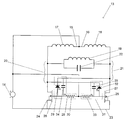
도 2에는 본 발명에 따른 유도 전력 송신기용 인버터(13)의 한 실시 예가 도시되어 있다. 상기 인버터는 도 1에 대해 고찰된 바와 같은 일반적인 유도 전력 송신기(2)에 적합할 수 있다. 그러나 당업자라면 어떠한 방식으로 상기 인버터가 유도 전력 송신기들의 다른 가능한 구성들에 적합할 수 있는지 또는 유도 전력 송신기들의 다른 가능한 구성들에서 작동하도록 구성 가능한지를 이해할 것이므로, 본 발명이 이 점에 대해 한정되어서는 아니 된다.2 shows an embodiment of an
상기 인버터(13)는 상기 인버터(13)의 잔여 부분에 DC 전력을 공급하기 위한 DC 전력 공급원(14)을 포함한다. 한 실시 예에서는, 상기 DC 전력 공급원이 AC-DC 변환기(예를 들면, 도 1에 대해 고찰된 바와 같은 AC-DC 변환기(5))일 수 있다. 상기 AC-DC 변환기의 동작은 적합한 제어기에 의해 제어될 수 있다. 여기서 이해할 점은 AC-DC 변환기가 상기 유도 전력 송신기의 특정 요건들에 따라 제어될 수 있다는 점이다. 예를 들면, 상기 인버터에 공급되는 DC 전력의 전류 또는 전압이 상기 유도 전력 송신기의 전력 요건들 또는 관련 유도 전력 수신기의 전력 요건들을 충족시키도록 상기 AC-DC 변환기가 제어될 수 있다.The inverter (13) includes a DC power supply (14) for supplying DC power to the remaining part of the inverter (13). In one embodiment, the DC power supply may be an AC-DC converter (e.g., AC-
상기 DC 전력 공급원(14)은 브리지 토폴로지(bridge topology)의 2개의 브랜치에 전류를 공급한다. 명확성을 위해 이들은 제1 브리지(15) 및 제2 브리지(16)로 지칭될 것이다. 각각의 브랜치는 DC 인덕터, 다시 말하면 제1 DC 인덕터(17) 및 제2 DC 인덕터(18)를 포함한다. 상기 DC 인덕터들은 상기 DC 전력 공급원에 의해 공급되는 평균 전류를 절반으로 분할한다. 여기서 이해할 점은 상기 DC 인덕터들의 효과가 이하에서 더 구체적으로 설명되겠지만 전류를 평활화하여 상기 전류를 상기 인버터의 잔여 부분에 대해 본질적으로 일정하게 한다는 점이다. 다시 말하면, 상기 인버터는 '전류-공급'을 받는다. 이해하겠지만, 이러한 DC 인덕터들이 공진에 관여되어 있지 않고 이하에서 설명되는 상기 공진 인덕터 및 공진 커패시터를 포함하는 공진 탱크와는 별개의 것이다.The
상기 인버터(13)는 제1 노드(20) 및 제2 노드(21)에 각각 존재하는 제1 브랜치 및 제2 브랜치(16) 사이에 접속된 공진 인버터(19)를 포함한다. 이하에서 더 구체적으로 설명되겠지만, 한 쌍의 스위치들의 스위칭으로 인해 상기 공진 인덕터를 통한 전류의 방향이 교번함으로써 결과적으로 AC 전류가 초래하게 된다. 상기 공진 인덕터는 공진 회로를 이루도록 공진 커패시터에 접속될 수 있다. 도 2에서는, 상기 공진 인덕터가 공진 커패시터(22)에 병렬로 접속되어 있다. 이하에서 더 구체적으로 고찰되겠지만, 높은 동작 주파수들에서, 상기 공진 커패시터는 상기 한 쌍의 스위치들의 커패시턴스에 의해 제공되는 공진을 가지고 상기 공진 커패시터가 제거될 수 있다. 유도 전력 송신기의 맥락에서, 상기 공진 인덕터는 송신 코일 또는 코일들일 수 있다.The
도 2에는 공통 접지(23)에 대하여 상기 제1 노드(20) 및 상기 제2 노드(21) 사이에 접속된 한 쌍의 스위치들이 또한 도시되어 있다. 명확성을 위해 이들은 각각 제1 스위치(24) 및 제2 스위치(25)로 지칭될 것이다. 당업자라면 이해하겠지만 상기 제1 스위치 및 상기 제2 스위치가 50% 듀티 사이클을 가지고 교번으로 스위치 온 및 스위치 오프되는 경우에, 결과적으로 상기 공진 인덕터(19)를 통해 AC 전류가 얻어지게 된다. 각각의 스위치 양단에 걸린 전압이 0일 때 각각의 스위치가 스위치 온(즉, 0 전압 스위치)되게 하기 위해, 상기 제1 노드 또는 제2 노드에 걸린 전압을 검출하는 것이 필요하다. 도 2에서는, 상기 제1 스위치 및 상기 제2 스위치 양자 모두가 제1 게이트(26) 또는 제2 게이트(27)에 걸린 전압을 각각 제어함으로써 스위치되는 n-채널 MOSFET들로서 도시되어 있다. 당업자라면 어떠한 방식으로 본 발명이 다른 타입들의 적합한 스위치들에 적응될 수 있는지를 이해할 것이므로, 본 발명이 이 점에 대해 한정되어서는 아니 된다.A pair of switches connected between the
도 2의 제1 스위치(24)를 참조하면, 상기 제1 게이트(26)는 제1 스위칭 회로(28)에 접속되어 있다. 상기 제1 스위칭 회로는 상기 제1 게이트의 전압을 제어하기 위한 제1 스위칭 신호를 생성함으로써 상기 제1 스위치의 스위칭을 제어하도록 구성되어 있다. 상기 제1 스위칭 회로는 상기 제2 노드(21)에 접속된 제1 다이오드(29) 및 상기 DC 전력 공급원(14)에 접속된 제1 전류 제한용 저항(30)을 포함한다.Referring to the
동작시, 상기 제2 노드(21)가 로우(low) 상태에 있을 때(다시 말하면, 상기 제2 스위치(25)가 온 상태에 있음으로써 상기 제2 노드가 접지(23)에 접속될 때), 상기 제1 다이오드(29)는 순방향으로 바이어스되고 그럼으로써 상기 제1 게이트(26)에 걸린 전압이 로우 상태에 있고, 그래서 결과적으로는 상기 제1 스위치(24)가 스위치 오프된다. 당업자라면 상기 제1 다이오드 양단 간의 순방향 바이어스 전압 때문에, 상기 제1 게이트에 걸린 전압이 0이 아닐 수 있지만, 상기 제1 다이오드에 따라, 상기 제1 게이트에 걸린 전압이 충분히 낮아지게 될 것임을 이해할 것이다. 다시 말하면, 상기 제1 스위칭 신호는 상기 제2 노드의 상태를 참조하고, 상기 제2 노드의 상태가 로우(low)일 경우에, 상기 제1 스위칭 신호는 상기 제2 노드에 기반을 두고 이루어진다.In operation, when the
그러나 상기 제2 노드(21)가 하이(high) 상태에 있을 때(다시 말하면, 상기 제2 스위치(25)가 스위치 오프되고 그럼으로써 전압이 상기 제2 노드에서 발생하게 될 때), 상기 제1 다이오드(29)는 역바이어스되고 그럼으로써 상기 제1 스위치(24)는 상기 제1 전류 제한용 저항(30)으로부터 전류를 인출하게 되고, 그래서 상기 제1 스위치는 하이 상태(다시 말하면, VDC - VR1)로 된다. 다시 말하면, 상기 제1 스위치 신호는 상기 제2 노드의 상태를 참조하고, 상기 제2 노드의 상태가 하이(high)일 경우에, 상기 제1 스위칭 신호는 상기 DC 전력 공급원(14)에 기반을 두고 이루어진다.However, when the
도 2의 제2 스위치(25)를 참조하면, 상기 제2 게이트(27)는 제2 스위칭 회로(31)에 접속되어 있다. 상기 제2 스위칭 회로는 상기 제2 게이트의 전압을 제어하기 위한 제2 스위칭 신호를 생성함으로써 상기 제2 스위치의 스위칭을 제어하도록 구성되어 있다. 상기 제2 스위칭 회로는 상기 제1 노드(20)에 접속된 제2 다이오드(32) 및 상기 DC 전력 공급원(14)에 접속된 제2 전류 제한용 저항(33)을 포함한다.Referring to the
동작시, 상기 제1 노드(20)가 로우(low) 상태에 있을 때(다시 말하면, 상기 제1 스위치(24)가 온 상태에 있음으로써 상기 제1 노드가 접지(23)에 접속될 때), 상기 제2 다이오드(32)는 순방향으로 바이어스되고 그럼으로써 상기 제2 게이트(27)에 걸린 전압이 또한 로우 상태에 있고, 결과적으로는 상기 제2 스위치(25)가 스위치 오프된다. 당업자라면 상기 제2 다이오드 양단 간의 순방향 바이어스 전압 때문에, 상기 제2 게이트에 걸린 전압이 0이 아닐 수 있지만, 상기 제2 다이오드에 따라, 상기 제2 게이트에 걸린 전압이 충분히 낮아지게 될 것임을 이해할 것이다. 다시 말하면, 상기 제2 스위칭 신호는 상기 제1 노드의 상태를 참조하고, 상기 제1 노드의 상태가 로우(low)일 경우에, 상기 제2 스위칭 신호는 상기 제1 노드에 기반을 두고 이루어진다.In operation, when the
그러나 상기 제1 노드(20)가 하이(high) 상태에 있을 때(다시 말하면, 상기 제1 스위치(24)가 스위치 오프되고 그럼으로써 전압이 상기 제1 노드에서 발생하게 될 때), 상기 제2 다이오드(32)는 역바이어스되고 그럼으로써 상기 제2 스위치(25)는 상기 제2 전류 제한용 저항(33)으로부터 전류를 인출하게 되고, 그래서 상기 제2 스위치는 하이 상태(다시 말하면, VDC - VR2)로 된다. 다시 말하면, 상기 제2 스위치 신호는 상기 제1 노드의 상태를 참조하고, 상기 제1 노드의 상태가 하이(high)일 경우에, 상기 제2 스위칭 신호는 상기 DC 전력 공급원(14)에 기반을 두고 이루어진다.However, when the
요컨대, 상기 제1 스위치(24)가 스위치 오프될 경우에, 이로 인해 고전압이 상기 제1 노드(20)에서 발생하게 된다. 상기 제1 노드가 하이 상태에 있게 되기 때문에, 상기 제2 스위치(25)는 스위치 온되고, 그래서 상기 제2 노드(21)가 로우 상태에 있게 된다. 상기 제1 노드가 로우 상태로 될 때, 상기 제2 스위치가 스위치 오프되고, 이로 인해 전압이 상기 제2 노드에서 발생하게 된다. 이러한 제2 노드가 하이 상태에 있게 되기 때문에, 상기 제1 스위치는 스위치 온되고 그래서 상기 제1 노드가 로우 상태에 있게 된다.That is, when the
당업자라면 상기 제1 스위칭 회로(28) 및 상기 제2 스위칭 회로(31)의 정미(正味; net) 효과는 상기 제1 스위치(24) 및 제2 스위치(25)가 실질적으로 교차결합되고, 각각의 스위치가 50% 듀티 사이클을 가지고 교번으로 스위치 오프 및 스위치 온되는 것임을 이해할 것이다. 더욱이 당업자라면 상기 스위치들의 스위칭이 상기 노드들(20, 21)에 걸린 전압에 의존하기 때문에, 0-전압 스위칭이 존재함을 이해할 것이다.Those skilled in the art will appreciate that the net effect of the
상기 회로의 정상 상태 동작에 관련된 파형들이 차후에 더 구체적으로 고찰될 것이다.Waveforms related to steady-state operation of the circuit will be discussed in greater detail later.
상기 인버터(13)의 다이오드들(29, 32)은 임의의 적절한 비대칭 전류 흐름 소자일 수 있다. 한 실시 예에서는 상기 다이오드들이 고주파 인버터에 의해 요구되는 고속 스위칭 및 저전압 강하에 대처하도록 쇼트키(Schottky) 다이오드들일 수 있다. 상기 다이오드들은 속도 향상용 커패시터들로서 작용하도록 하는 병렬 커패시터들을 포함할 수 있다. 도 2에는 상기 제1 다이오드(29) 및 제2 다이오드(32)에 각각 연관된 제1 속도 향상용 커패시터(34) 및 제2 속도 향상용 커패시터(35)가 도시되어 있다. 당업자라면 그러한 속도 향상용 커패시터들이 상기 스위치들의 스위치 온 속도를 향상시킴을 이해할 것이다. 또, 이는 고속 스위칭이 고주파 인버터에서 요구될 경우에 특히 바람직할 수 있다.The
도 2에서는, 상기 제1 스위칭 회로(28) 및 제2 스위칭 회로(31)가 상기 DC 전력 공급원(14)에 접속되어 있고 그럼으로써 상기 제1 스위칭 신호 및 제2 스위칭 신호가 상기 DC 전력 공급원의 전압에 기반을 두고 이루어지게 된다. 당업자라면 임의의 DC 소스가 적합할 수 있음을 이해할 것이다. 상기 DC 전력 공급원이 고 입력 전압을 지니는 일부 실시 예들에서는, 상기 제1 스위칭 회로 및 상기 제2 스위칭 회로에 접속된 개별 DC 소스(도 2에 도시되지 않음)를 지니는 것이 바람직할 수 있다. 예를 들면, 고전력 IPT 시스템들의 경우에는, 상기 DC 전력 공급원이 상기 스위치들에 비해 매우 높은 전압으로 상기 인버터에 전력을 공급할 필요가 있을 수 있고 그럼으로써, 상기 스위치들에 접속된 개별 DC 전력 공급원이 적합할 수 있다.2, the
당업자라면 어떠한 방식으로 구성요소들의 상대적인 크기들이 특정한 인버터의 요건들에 기반을 두고 선택되어야 할지를 이해할 것이므로, 본 발명이 이 점에 대해 한정되어서는 아니 된다. 인버터 회로는 이하의 인자들, 즉 DC 전력 공급원, 사용된 스위치 타입들, 사용된 다이오드 타입들, 속도 제한용 저항의 크기, 속도 향상용 커패시터들의 크기, 공진 인덕터의 크기, 전력 손실의 허용오차들, 스위칭 주파수들, 및 필요한 AC 전류 파형을 포함하는 인자들 중의 적어도 일부를 고려하여 구성될 수 있다.The skilled artisan will understand in what ways the relative sizes of the components should be selected based on the requirements of a particular inverter, so the invention should not be limited in this respect. The inverter circuit uses the following factors: the DC power source, the switch types used, the diode types used, the size of the resistor for speed limiting, the size of the capacitors for speed improvement, the size of the resonant inductor, , Switching frequencies, and at least some of the factors including the required AC current waveform.
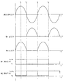
도 3에는 도 2의 인버터의 정상 상태 동작에 연관된 파형들이 도시되어 있다.Figure 3 shows waveforms associated with steady-state operation of the inverter of Figure 2.
시간 t1에서, 상기 제2 노드에 걸린 전압은 하이(high)이고, 그래서 결과적으로는 상기 제1 게이트 전압이 상기 DC 전력 공급원에 기반을 두고 이루어지며, 결과적으로는 VDC-VR1이 된다. 상기 제1 게이트 전압이 하이이므로, 상기 제1 스위치가 스위치 온되고, 결과적으로는 상기 제1 노드가 접지에 접속된다. 상기 제1 노드의 상태가 로우이므로, 상기 제2 다이오드는 순방향으로 바이어스되고, 결과적으로는 상기 제2 게이트 전압이 VD2가 되고, 상기 제2 스위치는 스위치 오프된다.At time t 1, the voltage is high (high) it took the second node, so as a result, the first gate voltage is made based on the DC power supply source, as a result, V is a DC -VR 1 . Since the first gate voltage is high, the first switch is switched on, and consequently, the first node is connected to the ground. Since the state of the first node is low, the second diode is biased in the forward direction, resulting in the second gate voltage being V D2 , and the second switch being switched off.
시간 t2에서, 상기 제2 노드에 걸린(그리고 상기 공진 인덕터 양단에 걸린) 전압은 0에 이르게 된다. 이러한 스테이지에서, 상기 제1 다이오드는 순방향으로 바이어스되고 그래서 상기 제1 다이오드 전압이 VD1이 되고 상기 제1 스위치는 스위치 오프된다. 상기 제1 스위치가 스위치 오프되므로, 전압이 상기 제1 노드에 발생하게 된다. 상기 제1 노드에 걸린 전압이 하이이므로, 상기 제2 다이오드는 역방향으로 바이어스되고 상기 제2 게이트 전압이 상기 DC 전력 공급원에 기반을 두고 이루어지게 되고, 결과적으로는 VDC-VR2가 된다.At time t 2, the first (and taken across the resonant inductor), the voltage across the second node is brought to zero. In this stage, the first diode is biased forward, so that the first diode voltage is V D1 and the first switch is switched off. As the first switch is switched off, a voltage is generated at the first node. Because the voltage across the first node is high, the second diode is biased in the reverse direction and the second gate voltage is made based on the DC power source, resulting in V DC -VR 2 .
시간 t3에서, 상기 제1 노드에 걸린(그리고 상기 공진 인덕터 양단에 걸린) 전압은 0에 이르게 된다. 이러한 스테이지에서, 상기 제2 다이오드는 순방향으로 바이어스되고 그래서 상기 제2 다이오드 전압이 VD2가 되며 상기 제2 스위치는 스위치 오프된다. 상기 제2 스위치가 스위치 오프되므로, 전압이 상기 제2 노드에 발생하게 된다. 상기 제2 노드에 걸린 전압이 하이(high)이므로, 상기 제1 다이오드는 역바이어스되고 상기 제1 게이트 전압은 상기 DC 전력 공급원에 기반을 두고 이루어지게 되며, 결과적으로는 VDC-VR1이 된다.At time t 3, wherein the voltage across the first node (and taken across the resonant inductor) is brought to zero. In this stage, the second diode is biased in the forward direction so that the second diode voltage is V D2 and the second switch is switched off. Since the second switch is switched off, a voltage is generated at the second node. Since the voltage across the second node is high, the first diode is reverse biased and the first gate voltage is made based on the DC power source, resulting in V DC -VR 1 .
시간 t4에서, 시간 t2와 동일한 상황이 적용된다. 따라서 스위칭 주기가 반복하게 된다. 당업자라면 도 3의 파형들로부터 상기 제1 스위칭 회로 및 상기 제2 스위칭 회로의 동작이 0 전압 스위칭을 유지함을 이해할 것이다. 예를 들면, 상기 제1 스위치는 일단 상기 제2 스위치가 스위치 온되면 단지 스위치 오프되게 될 뿐이다(이는 결과적으로 상기 제1 스위치 양단에 걸린 전압이 0이 될 것을 요구한다). 더욱이, 상기 제1 스위치 및 제2 스위치의 스위칭은 완전히 자율적이고 전용 제어기가 "영점 교차(zero-crossing)들"을 검출하거나 게이트 신호들을 제어하는 것을 요구하지 않는다. 상기 인버터는 상기 인버터에 공급되는 DC 전력이 존재하는 한 상기 인버터의 동작을 지속하게 된다.At time t 4, the same conditions and time t 2 is applied. Therefore, the switching cycle is repeated. It will be understood by those skilled in the art that the operation of the first switching circuit and the second switching circuit from the waveforms of FIG. 3 maintains zero voltage switching. For example, the first switch may only be switched off once the second switch is switched on (which eventually requires that the voltage across the first switch be zero). Moreover, switching of the first and second switches is completely autonomous and does not require the dedicated controller to detect "zero-crossings" or control gate signals. The inverter continues operation of the inverter as long as there is DC power supplied to the inverter.
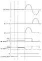
본 발명의 인버터는 복잡한 시동 회로를 요구하지 않고 자동으로 시동 가능하다. 도 4에는 시동 동안 전형적인 파형들이 도시되어 있다. 시간 t1'에서 시작하면, 양자 모두의 스위치들이 턴오프된다. 시간 t2'에서, 상기 DC 전력 공급원은 이때 스위치 온된다. 상기 제1 노드 및 상기 제2 노드 양자 모두가 로우 상태에 있으므로, 상기 제1 게이트 전압 및 상기 제2 게이트 전압은 상기 DC 전력 공급원에 기반을 두고 이루어지게 되고(VDC-iR/2), 양자 모두의 스위치들은 턴온하게 된다. 상기 DC 전력 공급원으로부터의 전류는 이때 상기 DC 인덕터들에서 형성하게 된다. 어떤 지점(시간 t3')에서, 제1 0점 교차는 (도 4에 도시된 바와 같이) 상기 제1 다이오드 또는 상기 제2 다이오드에 의해 검출하게 된다. 이로 인해 그러한 스위치에 대한 게이트 전압이 낮아지게 되고, 그러한 스위치(예컨대, 도 4의 제2 스위치)가 턴오프하게 된다. 다른 스위치의 게이트 전압은 (VDC-iR, 다시 말하면 VDC-VR로) 증가하게 되고 그러한 스위치(도 4의 제1 스위치)는 스위치 온 상태를 이루게 된다. 이로부터 도 3에 도시된 바와 같은 인버터의 정상 동작이 지속되게 된다. 당업자라면 이러한 시동 방법이 전용 시동 회로를 요구하지 않음을 이해할 것이다.The inverter of the present invention is automatically startable without requiring a complicated starting circuit. Figure 4 shows typical waveforms during start-up. Starting at time t 1 ' , both switches are turned off. At time t2 ' , the DC power supply is then switched on. Since both the first node and the second node are in a low state, the first gate voltage and the second gate voltage are made based on the DC power source (V DC -iR / 2) All of the switches are turned on. The current from the DC power source is then formed in the DC inductors. At some point (time t 3 ' ), the first zero crossings are detected by the first diode or the second diode (as shown in FIG. 4). This lowers the gate voltage for such a switch, and such a switch (e.g., the second switch of FIG. 4) is turned off. The gate voltage of the other switch is increased to (V DC -i R , in other words, V DC -V R ), and such a switch (the first switch in FIG. 4) is switched on. From this, the normal operation of the inverter as shown in FIG. 3 is continued. Those skilled in the art will appreciate that this starting method does not require a dedicated starter circuit.
위에서 설명한 인버터의 스위치들의 스위치 온이 2개의 전류 제한용 저항(다시 말하면, 도 2의 참조번호 30 및 33)을 통해 상기 DC 전력 공급원(또는 소정의 별도 DC 소스)에 의해 직접 구동되고, 위에서 설명한 인버터의 스위치들의 스위치 오프가 상기 다이오드들(다시 말하면, 도 2의 참조번호 29 및 32)을 통해 상기 스위치들(다시 말하면, 도 2의 참조번호 24 및 25)의 활성 상태의 단락에 의해 이루어지게 되므로, 스위칭 신호의 품질은 관련된 고 전력 손실 없이 고주파에서 유지될 수 있다. 따라서 상기 인버터는 고주파 상태하에서 동작할 수 있다. 한 실시 예에서는, 상기 인버터가 kHz 범위 내의 저주파, 예컨대 약 1 kHz에서부터 약 1000 kHz에 이르기까지의 범위 내의 주파수에서부터, MHz 범위 내의 고주파, 예컨대 약 10 MHz에서부터 약 100 MHz에 이르기까지의 범위 내의 고주파에 이르기까지 동작할 수 있다. 더욱이, 그러한 고주파에서, 상기 공진 인덕터와 공진하도록 대신 사용되는 상기 제1 스위치 및 상기 제2 스위치의 출력 커패시턴스를 가지고 상기 공진 인덕터에 접속되는 별도의 공진 커패시터를 제거하는 것이 가능할 수 있다.The switch-on of the switches of the above-described inverter is directly driven by the DC power supply (or a separate separate DC source) through the two current limiting resistors (i. E., 30 and 33 in Fig. 2) The switch off of the switches of the inverter is effected by an active short of the switches (i. E., 24 and 25 of Fig. 2) via the diodes (i. E., 29 and 32 of Fig. 2) , The quality of the switching signal can be maintained at high frequencies without associated high power loss. Therefore, the inverter can operate under a high frequency state. In one embodiment, the inverter is configured to operate from a low frequency in the kHz range, such as a frequency ranging from about 1 kHz to about 1000 kHz, to a high frequency within the MHz range, such as from about 10 MHz to about 100 MHz Lt; / RTI > Furthermore, at such a high frequency, it may be possible to remove a separate resonant capacitor connected to the resonant inductor with an output capacitance of the first switch and the second switch, which are used instead to resonate with the resonant inductor.
예를 들면, 도 5에는 91 kHz 및 10 MHz 각각에서 정상 상태 동작에 상응하는 파형들이 도시되어 있다. 상기 파형들은 상기 공진 인덕터 양단 간의 전압(v C ) 및 상기 공진 인덕터를 통한 전류(i L )를 보여준다. 알 수 있는 바와 같이, 주파수의 증가는 출력 파형의 품질에 거의 영향을 미치지 않는다.For example, FIG. 5 shows waveforms corresponding to steady state operation at 91 kHz and 10 MHz, respectively. The waveforms show the voltage ( v C ) across the resonant inductor and the current through the resonant inductor ( i L ). As can be seen, the increase in frequency has little effect on the quality of the output waveform.
당업자라면 위에서 설명한 인버터가 심지어 고주파에서도 영점 교차들을 검출하고 상기 스위치들을 제어하도록 하는 별도의 회로에 의존하지 않고 ZVS를 달성함을 이해할 것이다. 더욱이, 어떠한 별도의 회로도 존재하지 않으므로, 상기 인버터는 자율적이고 상기 인버터의 동작을 지속하게 된다. 마지막으로, 상기 인버터는 별도의 전용 시동 회로를 요구하지 않는 간단한 시동 절차를 지닌다.Those skilled in the art will appreciate that the inverter described above achieves ZVS without relying on a separate circuit to detect zero crossings and even control the switches at high frequencies. Furthermore, since there is no separate circuit, the inverter is autonomous and continues to operate the inverter. Finally, the inverter has a simple startup procedure that does not require a separate dedicated starter circuit.
본 발명이 본 발명의 실시 예들의 설명으로 예시되었고, 그리고 상기 실시 예들이 구체적으로 설명되었지만, 그러한 세부로 첨부된 청구항들의 범위를 한정하거나 어떠한 방식으로든 제한하는 것이 본원 출원인이 의도한 바가 아니다. 추가 이점들 및 변형들이 당업자에게는 쉽게 부각되게 된다. 그러므로 본 발명은 본 발명의 넓은 관점에서 도시되고 설명된 특정한 세부들, 대표적인 장치 및 방법, 그리고 전형적인 예들에 국한되지 않는다. 따라서, 본원 출원인의 총괄적 발명의 개념의 사상 또는 범위로부터 벗어나지 않는 일탈들이 그러한 세부들로부터 이루어질 수 있다.While the invention has been illustrated by the description of embodiments of the invention and these embodiments have been described in detail, it is not the intention of the applicant to limit or in any way limit the scope of the appended claims to such detail. Additional advantages and modifications will readily appear to those skilled in the art. Therefore, the present invention is not limited to the specific details, representative apparatus and method, and typical examples shown and described in the broader aspects of the present invention. Accordingly, departures may be made from such details without departing from the spirit or scope of the inventive concept of the generic invention of the present applicant.
Claims (10)
상기 푸시-풀 인버터는,
a. 제1 브랜치 및 제2 브랜치에 전력을 공급하는 DC 전력 공급원;
b. 상기 제1 브랜치 상의 제1 노드 및 상기 제2 브랜치 상의 제2 노드 간에 접속된 공진 인버터;
c. 제1 스위칭 신호에 의해 스위칭되는 제1 스위치로서, 상기 제1 노드 및 공통 접지 사이에 접속된, 제1 스위치; 및
d. 제2 스위칭 신호에 의해 스위칭되는 제2 스위치로서, 상기 제2 노드 및 상기 공통 접지 사이에 접속된, 제2 스위치;
를 포함하며,
상기 제1 스위칭 신호는 상기 제2 노드가 로우(low) 상태에 있을 때 상기 제2 노드에 기반을 두고 이루어지고 상기 제2 노드가 하이(high) 상태에 있을 때 DC 소스에 기반을 두고 이루어지며, 상기 제2 스위칭 신호는 상기 제1 노드가 로우(low) 상태에 있을 때 상기 제1 노드에 기반을 두고 이루어지고 상기 제1 노드가 하이(high) 상태에 있을 때 DC 소스에 기반을 두고 이루어지는, 유도 전력 송신기용 푸시-풀 인버터.A push-pull inverter for an inductive power transmitter,
The push-pull inverter includes:
a. A DC power supply for supplying power to the first branch and the second branch;
b. A resonant inverter connected between a first node on the first branch and a second node on the second branch;
c. A first switch that is switched by a first switching signal, the first switch connected between the first node and a common ground; And
d. A second switch that is switched by a second switching signal, the second switch being connected between the second node and the common ground;
/ RTI >
The first switching signal is based on the second node when the second node is in a low state and is based on a DC source when the second node is in a high state, , The second switching signal being based on the first node when the first node is in a low state and being based on a DC source when the first node is in a high state, , A push-pull inverter for an inductive power transmitter.
Applications Claiming Priority (3)
| Application Number | Priority Date | Filing Date | Title |
|---|---|---|---|
| US201361909709P | 2013-11-27 | 2013-11-27 | |
| US61/909,709 | 2013-11-27 | ||
| PCT/NZ2014/000231 WO2015080598A1 (en) | 2013-11-27 | 2014-11-07 | Inverter for inductive power transmitter |
Publications (1)
| Publication Number | Publication Date |
|---|---|
| KR20160091381A true KR20160091381A (en) | 2016-08-02 |
Family
ID=53199427
Family Applications (1)
| Application Number | Title | Priority Date | Filing Date |
|---|---|---|---|
| KR1020167016979A KR20160091381A (en) | 2013-11-27 | 2014-11-07 | Inverter for inductive power transmitter |
Country Status (6)
| Country | Link |
|---|---|
| US (1) | US20170264140A1 (en) |
| EP (1) | EP3075070A4 (en) |
| JP (1) | JP2017503459A (en) |
| KR (1) | KR20160091381A (en) |
| CN (1) | CN105765845A (en) |
| WO (1) | WO2015080598A1 (en) |
Families Citing this family (2)
| Publication number | Priority date | Publication date | Assignee | Title |
|---|---|---|---|---|
| WO2016056925A1 (en) | 2014-10-08 | 2016-04-14 | Powerbyproxi Limited | Inverter for inductive power transmitter |
| DE102016210639A1 (en) * | 2016-06-15 | 2017-12-21 | Robert Bosch Gmbh | loader |
Family Cites Families (7)
| Publication number | Priority date | Publication date | Assignee | Title |
|---|---|---|---|---|
| US4447741A (en) * | 1982-09-27 | 1984-05-08 | Northern Telecom Limited | Base drive circuit for power transistors |
| JPS62269417A (en) * | 1986-05-16 | 1987-11-21 | Sumitomo Electric Ind Ltd | Drive circuit for circuit element having diode characteristic |
| US6317347B1 (en) * | 2000-10-06 | 2001-11-13 | Philips Electronics North America Corporation | Voltage feed push-pull resonant inverter for LCD backlighting |
| US7180759B2 (en) * | 2004-11-03 | 2007-02-20 | Square D Company | Push-pull inverter with snubber energy recovery |
| US7628340B2 (en) * | 2006-02-27 | 2009-12-08 | Continental Automotive Systems Us, Inc. | Constant current zero-voltage switching induction heater driver for variable spray injection |
| CN104040863B (en) * | 2011-11-10 | 2018-06-22 | 苹果公司 | For controlling the method for converter |
| CN103337964A (en) * | 2013-04-27 | 2013-10-02 | 南京航空航天大学 | Ultrahigh frequency isolation push-pull resonant power converter |
-
2014
- 2014-11-07 EP EP14866034.3A patent/EP3075070A4/en not_active Withdrawn
- 2014-11-07 US US15/039,965 patent/US20170264140A1/en not_active Abandoned
- 2014-11-07 WO PCT/NZ2014/000231 patent/WO2015080598A1/en active Application Filing
- 2014-11-07 CN CN201480064771.5A patent/CN105765845A/en active Pending
- 2014-11-07 JP JP2016534718A patent/JP2017503459A/en active Pending
- 2014-11-07 KR KR1020167016979A patent/KR20160091381A/en not_active Application Discontinuation
Also Published As
| Publication number | Publication date |
|---|---|
| EP3075070A1 (en) | 2016-10-05 |
| US20170264140A1 (en) | 2017-09-14 |
| JP2017503459A (en) | 2017-01-26 |
| EP3075070A4 (en) | 2017-08-16 |
| CN105765845A (en) | 2016-07-13 |
| WO2015080598A1 (en) | 2015-06-04 |
Similar Documents
| Publication | Publication Date | Title |
|---|---|---|
| US5946206A (en) | Plural parallel resonant switching power supplies | |
| RU2672260C2 (en) | On and off controlled resonant dc-dc power converter | |
| RU2467459C2 (en) | Conversion circuit and system with such conversion circuit | |
| US9019736B2 (en) | DC-to-AC power conversion system and method of operating the same | |
| US8619438B2 (en) | Resonant converter | |
| US9300225B2 (en) | Solar photovoltaic power conversion system and method of operating the same | |
| US20080043506A1 (en) | Dc-ac converter | |
| KR20140090669A (en) | A method for controlling a converter | |
| WO2010069096A1 (en) | Fixed-frequency llc resonant power regulator | |
| CN107078651A (en) | Converter | |
| US20130077356A1 (en) | Dc-dc converters | |
| US11128172B2 (en) | Power transmitter and method for wirelessly transferring power | |
| US9214868B2 (en) | Power supply device | |
| US20160049858A1 (en) | Lc resonant converter using phase shift switching method | |
| WO2013098647A2 (en) | Resonant bi-directional dc-ac converter | |
| KR20110076972A (en) | Converter circuit and unit and system comprising such converter circuit | |
| KR20160091381A (en) | Inverter for inductive power transmitter | |
| CN104584405A (en) | Switching control circuit and switching power device | |
| US20170250618A1 (en) | Extremely-Sparse Parallel AC-Link Power Converter | |
| JP2018509876A (en) | Inductive power receiver | |
| US7361870B2 (en) | Supply generator for an oscillating circuit, particularly for an induction cooking hob | |
| JP2004274864A (en) | Switching power unit | |
| JP7237545B2 (en) | Electric vehicle power supply | |
| US20180048225A1 (en) | Method and system for bridgeless ac-dc converter | |
| JP2010259317A (en) | Load driver |
Legal Events
| Date | Code | Title | Description |
|---|---|---|---|
| WITN | Application deemed withdrawn, e.g. because no request for examination was filed or no examination fee was paid |