KR20160043576A - Liquid crystal display and manufacturing method thereof - Google Patents
Liquid crystal display and manufacturing method thereof Download PDFInfo
- Publication number
- KR20160043576A KR20160043576A KR1020140137545A KR20140137545A KR20160043576A KR 20160043576 A KR20160043576 A KR 20160043576A KR 1020140137545 A KR1020140137545 A KR 1020140137545A KR 20140137545 A KR20140137545 A KR 20140137545A KR 20160043576 A KR20160043576 A KR 20160043576A
- Authority
- KR
- South Korea
- Prior art keywords
- insulating film
- electrode
- gate electrode
- pixel electrode
- data line
- Prior art date
Links
- 239000004973 liquid crystal related substance Substances 0.000 title claims abstract description 53
- 238000004519 manufacturing process Methods 0.000 title description 9
- 229910052581 Si3N4 Inorganic materials 0.000 claims abstract description 25
- HQVNEWCFYHHQES-UHFFFAOYSA-N silicon nitride Chemical compound N12[Si]34N5[Si]62N3[Si]51N64 HQVNEWCFYHHQES-UHFFFAOYSA-N 0.000 claims abstract description 25
- 239000004065 semiconductor Substances 0.000 claims abstract description 22
- 239000000758 substrate Substances 0.000 claims abstract description 21
- 125000001153 fluoro group Chemical group F* 0.000 claims abstract description 14
- 230000001681 protective effect Effects 0.000 claims abstract description 13
- 238000000034 method Methods 0.000 claims description 23
- 125000004429 atom Chemical group 0.000 claims description 16
- 239000007789 gas Substances 0.000 claims description 8
- IJGRMHOSHXDMSA-UHFFFAOYSA-N Atomic nitrogen Chemical compound N#N IJGRMHOSHXDMSA-UHFFFAOYSA-N 0.000 claims description 6
- ABTOQLMXBSRXSM-UHFFFAOYSA-N silicon tetrafluoride Chemical compound F[Si](F)(F)F ABTOQLMXBSRXSM-UHFFFAOYSA-N 0.000 claims description 6
- 230000000903 blocking effect Effects 0.000 claims description 4
- 238000002161 passivation Methods 0.000 claims description 4
- 230000001678 irradiating effect Effects 0.000 claims description 2
- 239000011149 active material Substances 0.000 claims 1
- 239000010408 film Substances 0.000 description 91
- 239000010410 layer Substances 0.000 description 36
- 229910004205 SiNX Inorganic materials 0.000 description 13
- 239000010409 thin film Substances 0.000 description 11
- 230000005684 electric field Effects 0.000 description 9
- 229910045601 alloy Inorganic materials 0.000 description 6
- 239000000956 alloy Substances 0.000 description 6
- 239000011521 glass Substances 0.000 description 6
- 238000002834 transmittance Methods 0.000 description 6
- ZOKXTWBITQBERF-UHFFFAOYSA-N Molybdenum Chemical compound [Mo] ZOKXTWBITQBERF-UHFFFAOYSA-N 0.000 description 5
- 229910052750 molybdenum Inorganic materials 0.000 description 5
- 239000011733 molybdenum Substances 0.000 description 5
- 239000010936 titanium Substances 0.000 description 5
- 229910001413 alkali metal ion Inorganic materials 0.000 description 4
- 229910052782 aluminium Inorganic materials 0.000 description 4
- XAGFODPZIPBFFR-UHFFFAOYSA-N aluminium Chemical compound [Al] XAGFODPZIPBFFR-UHFFFAOYSA-N 0.000 description 4
- 239000011651 chromium Substances 0.000 description 4
- 238000009792 diffusion process Methods 0.000 description 4
- 229910052751 metal Inorganic materials 0.000 description 4
- 239000002184 metal Substances 0.000 description 4
- VYZAMTAEIAYCRO-UHFFFAOYSA-N Chromium Chemical compound [Cr] VYZAMTAEIAYCRO-UHFFFAOYSA-N 0.000 description 3
- 229910004298 SiO 2 Inorganic materials 0.000 description 3
- VYPSYNLAJGMNEJ-UHFFFAOYSA-N Silicium dioxide Chemical compound O=[Si]=O VYPSYNLAJGMNEJ-UHFFFAOYSA-N 0.000 description 3
- 229910020923 Sn-O Inorganic materials 0.000 description 3
- RTAQQCXQSZGOHL-UHFFFAOYSA-N Titanium Chemical compound [Ti] RTAQQCXQSZGOHL-UHFFFAOYSA-N 0.000 description 3
- 229910052804 chromium Inorganic materials 0.000 description 3
- 239000010949 copper Substances 0.000 description 3
- 239000013039 cover film Substances 0.000 description 3
- 238000010586 diagram Methods 0.000 description 3
- 229910001195 gallium oxide Inorganic materials 0.000 description 3
- 230000003071 parasitic effect Effects 0.000 description 3
- 229910052814 silicon oxide Inorganic materials 0.000 description 3
- 229910052715 tantalum Inorganic materials 0.000 description 3
- GUVRBAGPIYLISA-UHFFFAOYSA-N tantalum atom Chemical compound [Ta] GUVRBAGPIYLISA-UHFFFAOYSA-N 0.000 description 3
- 229910052719 titanium Inorganic materials 0.000 description 3
- YVTHLONGBIQYBO-UHFFFAOYSA-N zinc indium(3+) oxygen(2-) Chemical compound [O--].[Zn++].[In+3] YVTHLONGBIQYBO-UHFFFAOYSA-N 0.000 description 3
- 229910000838 Al alloy Inorganic materials 0.000 description 2
- RYGMFSIKBFXOCR-UHFFFAOYSA-N Copper Chemical compound [Cu] RYGMFSIKBFXOCR-UHFFFAOYSA-N 0.000 description 2
- 206010047571 Visual impairment Diseases 0.000 description 2
- 229910007541 Zn O Inorganic materials 0.000 description 2
- 238000000137 annealing Methods 0.000 description 2
- 239000004020 conductor Substances 0.000 description 2
- 229910052802 copper Inorganic materials 0.000 description 2
- 229910052731 fluorine Inorganic materials 0.000 description 2
- AMGQUBHHOARCQH-UHFFFAOYSA-N indium;oxotin Chemical compound [In].[Sn]=O AMGQUBHHOARCQH-UHFFFAOYSA-N 0.000 description 2
- 239000000463 material Substances 0.000 description 2
- 239000011368 organic material Substances 0.000 description 2
- 239000011241 protective layer Substances 0.000 description 2
- 239000003870 refractory metal Substances 0.000 description 2
- HGCGQDMQKGRJNO-UHFFFAOYSA-N xenon monochloride Chemical compound [Xe]Cl HGCGQDMQKGRJNO-UHFFFAOYSA-N 0.000 description 2
- 229910001316 Ag alloy Inorganic materials 0.000 description 1
- 229910000881 Cu alloy Inorganic materials 0.000 description 1
- GYHNNYVSQQEPJS-UHFFFAOYSA-N Gallium Chemical compound [Ga] GYHNNYVSQQEPJS-UHFFFAOYSA-N 0.000 description 1
- BQCADISMDOOEFD-UHFFFAOYSA-N Silver Chemical compound [Ag] BQCADISMDOOEFD-UHFFFAOYSA-N 0.000 description 1
- ATJFFYVFTNAWJD-UHFFFAOYSA-N Tin Chemical compound [Sn] ATJFFYVFTNAWJD-UHFFFAOYSA-N 0.000 description 1
- 229910007746 Zr—O Inorganic materials 0.000 description 1
- DZLPZFLXRVRDAE-UHFFFAOYSA-N [O--].[O--].[O--].[O--].[Al+3].[Zn++].[In+3] Chemical compound [O--].[O--].[O--].[O--].[Al+3].[Zn++].[In+3] DZLPZFLXRVRDAE-UHFFFAOYSA-N 0.000 description 1
- AWTYVENYAIZTAE-UHFFFAOYSA-N [Zr].[Sn]=O.[In] Chemical compound [Zr].[Sn]=O.[In] AWTYVENYAIZTAE-UHFFFAOYSA-N 0.000 description 1
- 239000011248 coating agent Substances 0.000 description 1
- 238000000576 coating method Methods 0.000 description 1
- 229910052733 gallium Inorganic materials 0.000 description 1
- 229910052732 germanium Inorganic materials 0.000 description 1
- GNPVGFCGXDBREM-UHFFFAOYSA-N germanium atom Chemical compound [Ge] GNPVGFCGXDBREM-UHFFFAOYSA-N 0.000 description 1
- WCOSNLGKHNWDQR-UHFFFAOYSA-N germanium;indium;oxotin Chemical compound [Ge].[In].[Sn]=O WCOSNLGKHNWDQR-UHFFFAOYSA-N 0.000 description 1
- 229910052735 hafnium Inorganic materials 0.000 description 1
- VBJZVLUMGGDVMO-UHFFFAOYSA-N hafnium atom Chemical compound [Hf] VBJZVLUMGGDVMO-UHFFFAOYSA-N 0.000 description 1
- HJZPJSFRSAHQNT-UHFFFAOYSA-N indium(3+) oxygen(2-) zirconium(4+) Chemical compound [O-2].[Zr+4].[In+3] HJZPJSFRSAHQNT-UHFFFAOYSA-N 0.000 description 1
- 229910010272 inorganic material Inorganic materials 0.000 description 1
- 239000011147 inorganic material Substances 0.000 description 1
- 239000011159 matrix material Substances 0.000 description 1
- 239000007769 metal material Substances 0.000 description 1
- 150000002739 metals Chemical class 0.000 description 1
- 238000002156 mixing Methods 0.000 description 1
- 238000012986 modification Methods 0.000 description 1
- 230000004048 modification Effects 0.000 description 1
- TWNQGVIAIRXVLR-UHFFFAOYSA-N oxo(oxoalumanyloxy)alumane Chemical compound O=[Al]O[Al]=O TWNQGVIAIRXVLR-UHFFFAOYSA-N 0.000 description 1
- BPUBBGLMJRNUCC-UHFFFAOYSA-N oxygen(2-);tantalum(5+) Chemical compound [O-2].[O-2].[O-2].[O-2].[O-2].[Ta+5].[Ta+5] BPUBBGLMJRNUCC-UHFFFAOYSA-N 0.000 description 1
- 230000000704 physical effect Effects 0.000 description 1
- 230000003252 repetitive effect Effects 0.000 description 1
- VSZWPYCFIRKVQL-UHFFFAOYSA-N selanylidenegallium;selenium Chemical compound [Se].[Se]=[Ga].[Se]=[Ga] VSZWPYCFIRKVQL-UHFFFAOYSA-N 0.000 description 1
- 229910001936 tantalum oxide Inorganic materials 0.000 description 1
- JBQYATWDVHIOAR-UHFFFAOYSA-N tellanylidenegermanium Chemical compound [Te]=[Ge] JBQYATWDVHIOAR-UHFFFAOYSA-N 0.000 description 1
- OPCPDIFRZGJVCE-UHFFFAOYSA-N zinc indium(3+) oxygen(2-) titanium(4+) Chemical compound [O-2].[Zn+2].[In+3].[Ti+4] OPCPDIFRZGJVCE-UHFFFAOYSA-N 0.000 description 1
- XLOMVQKBTHCTTD-UHFFFAOYSA-N zinc oxide Inorganic materials [Zn]=O XLOMVQKBTHCTTD-UHFFFAOYSA-N 0.000 description 1
- 239000011787 zinc oxide Substances 0.000 description 1
Images


Classifications
-
- H—ELECTRICITY
- H01—ELECTRIC ELEMENTS
- H01L—SEMICONDUCTOR DEVICES NOT COVERED BY CLASS H10
- H01L29/00—Semiconductor devices adapted for rectifying, amplifying, oscillating or switching, or capacitors or resistors with at least one potential-jump barrier or surface barrier, e.g. PN junction depletion layer or carrier concentration layer; Details of semiconductor bodies or of electrodes thereof ; Multistep manufacturing processes therefor
- H01L29/66—Types of semiconductor device ; Multistep manufacturing processes therefor
- H01L29/66007—Multistep manufacturing processes
- H01L29/66969—Multistep manufacturing processes of devices having semiconductor bodies not comprising group 14 or group 13/15 materials
-
- H—ELECTRICITY
- H01—ELECTRIC ELEMENTS
- H01L—SEMICONDUCTOR DEVICES NOT COVERED BY CLASS H10
- H01L27/00—Devices consisting of a plurality of semiconductor or other solid-state components formed in or on a common substrate
- H01L27/02—Devices consisting of a plurality of semiconductor or other solid-state components formed in or on a common substrate including semiconductor components specially adapted for rectifying, oscillating, amplifying or switching and having at least one potential-jump barrier or surface barrier; including integrated passive circuit elements with at least one potential-jump barrier or surface barrier
- H01L27/12—Devices consisting of a plurality of semiconductor or other solid-state components formed in or on a common substrate including semiconductor components specially adapted for rectifying, oscillating, amplifying or switching and having at least one potential-jump barrier or surface barrier; including integrated passive circuit elements with at least one potential-jump barrier or surface barrier the substrate being other than a semiconductor body, e.g. an insulating body
- H01L27/1214—Devices consisting of a plurality of semiconductor or other solid-state components formed in or on a common substrate including semiconductor components specially adapted for rectifying, oscillating, amplifying or switching and having at least one potential-jump barrier or surface barrier; including integrated passive circuit elements with at least one potential-jump barrier or surface barrier the substrate being other than a semiconductor body, e.g. an insulating body comprising a plurality of TFTs formed on a non-semiconducting substrate, e.g. driving circuits for AMLCDs
- H01L27/1222—Devices consisting of a plurality of semiconductor or other solid-state components formed in or on a common substrate including semiconductor components specially adapted for rectifying, oscillating, amplifying or switching and having at least one potential-jump barrier or surface barrier; including integrated passive circuit elements with at least one potential-jump barrier or surface barrier the substrate being other than a semiconductor body, e.g. an insulating body comprising a plurality of TFTs formed on a non-semiconducting substrate, e.g. driving circuits for AMLCDs with a particular composition, shape or crystalline structure of the active layer
- H01L27/1225—Devices consisting of a plurality of semiconductor or other solid-state components formed in or on a common substrate including semiconductor components specially adapted for rectifying, oscillating, amplifying or switching and having at least one potential-jump barrier or surface barrier; including integrated passive circuit elements with at least one potential-jump barrier or surface barrier the substrate being other than a semiconductor body, e.g. an insulating body comprising a plurality of TFTs formed on a non-semiconducting substrate, e.g. driving circuits for AMLCDs with a particular composition, shape or crystalline structure of the active layer with semiconductor materials not belonging to the group IV of the periodic table, e.g. InGaZnO
-
- H—ELECTRICITY
- H01—ELECTRIC ELEMENTS
- H01L—SEMICONDUCTOR DEVICES NOT COVERED BY CLASS H10
- H01L29/00—Semiconductor devices adapted for rectifying, amplifying, oscillating or switching, or capacitors or resistors with at least one potential-jump barrier or surface barrier, e.g. PN junction depletion layer or carrier concentration layer; Details of semiconductor bodies or of electrodes thereof ; Multistep manufacturing processes therefor
- H01L29/66—Types of semiconductor device ; Multistep manufacturing processes therefor
- H01L29/68—Types of semiconductor device ; Multistep manufacturing processes therefor controllable by only the electric current supplied, or only the electric potential applied, to an electrode which does not carry the current to be rectified, amplified or switched
- H01L29/76—Unipolar devices, e.g. field effect transistors
- H01L29/772—Field effect transistors
- H01L29/78—Field effect transistors with field effect produced by an insulated gate
- H01L29/786—Thin film transistors, i.e. transistors with a channel being at least partly a thin film
- H01L29/78606—Thin film transistors, i.e. transistors with a channel being at least partly a thin film with supplementary region or layer in the thin film or in the insulated bulk substrate supporting it for controlling or increasing the safety of the device
- H01L29/78633—Thin film transistors, i.e. transistors with a channel being at least partly a thin film with supplementary region or layer in the thin film or in the insulated bulk substrate supporting it for controlling or increasing the safety of the device with a light shield
-
- H—ELECTRICITY
- H01—ELECTRIC ELEMENTS
- H01L—SEMICONDUCTOR DEVICES NOT COVERED BY CLASS H10
- H01L29/00—Semiconductor devices adapted for rectifying, amplifying, oscillating or switching, or capacitors or resistors with at least one potential-jump barrier or surface barrier, e.g. PN junction depletion layer or carrier concentration layer; Details of semiconductor bodies or of electrodes thereof ; Multistep manufacturing processes therefor
- H01L29/66—Types of semiconductor device ; Multistep manufacturing processes therefor
- H01L29/68—Types of semiconductor device ; Multistep manufacturing processes therefor controllable by only the electric current supplied, or only the electric potential applied, to an electrode which does not carry the current to be rectified, amplified or switched
- H01L29/76—Unipolar devices, e.g. field effect transistors
- H01L29/772—Field effect transistors
- H01L29/78—Field effect transistors with field effect produced by an insulated gate
- H01L29/786—Thin film transistors, i.e. transistors with a channel being at least partly a thin film
- H01L29/78645—Thin film transistors, i.e. transistors with a channel being at least partly a thin film with multiple gate
- H01L29/78648—Thin film transistors, i.e. transistors with a channel being at least partly a thin film with multiple gate arranged on opposing sides of the channel
-
- H—ELECTRICITY
- H01—ELECTRIC ELEMENTS
- H01L—SEMICONDUCTOR DEVICES NOT COVERED BY CLASS H10
- H01L29/00—Semiconductor devices adapted for rectifying, amplifying, oscillating or switching, or capacitors or resistors with at least one potential-jump barrier or surface barrier, e.g. PN junction depletion layer or carrier concentration layer; Details of semiconductor bodies or of electrodes thereof ; Multistep manufacturing processes therefor
- H01L29/66—Types of semiconductor device ; Multistep manufacturing processes therefor
- H01L29/68—Types of semiconductor device ; Multistep manufacturing processes therefor controllable by only the electric current supplied, or only the electric potential applied, to an electrode which does not carry the current to be rectified, amplified or switched
- H01L29/76—Unipolar devices, e.g. field effect transistors
- H01L29/772—Field effect transistors
- H01L29/78—Field effect transistors with field effect produced by an insulated gate
- H01L29/786—Thin film transistors, i.e. transistors with a channel being at least partly a thin film
- H01L29/7869—Thin film transistors, i.e. transistors with a channel being at least partly a thin film having a semiconductor body comprising an oxide semiconductor material, e.g. zinc oxide, copper aluminium oxide, cadmium stannate
Abstract
Description
본 발명은 액정 표시 장치 및 그 제조 방법에 관한 것이다.The present invention relates to a liquid crystal display device and a manufacturing method thereof.
액정 표시 장치(Liquid Crystal Display)는 현재 가장 널리 사용되고 있는 평판 표시 장치(Flat Panel Display) 중 하나로서, 전극에 전압을 인가하여 액정층의 액정 분자들을 재배열시킴으로써 투과되는 빛의 양을 조절하는 표시 장치이다.BACKGROUND ART [0002] A liquid crystal display (LCD) is one of the most widely used flat panel displays. The liquid crystal display displays liquid crystal molecules in a liquid crystal layer by applying voltage to electrodes, Device.
액정 표시 장치는 박형화가 용이한 장점을 지니고 있지만, 전면 시인성에 비해 측면 시인성이 떨어지는 단점이 있어 이를 극복하기 위한 다양한 방식의 액정 배열 및 구동 방법이 개발되고 있다. 이러한 광시야각을 구현하기 위한 방법으로서, 화소 전극 및 공통 전극을 하나의 기판에 형성하는 액정 표시 장치가 주목받고 있다. The liquid crystal display device has the advantage of being easy to be thinned, but has a disadvantage that the side visibility is lower than that of the front view, and various arrangements of the liquid crystal array and the driving method for overcoming this are being developed. As a method for realizing such a wide viewing angle, a liquid crystal display device in which a pixel electrode and a common electrode are formed on one substrate has attracted attention.
이러한 액정 표시 장치에서 자기 정렬 하단 게이트 공정(Self Aligned Bottom Gate)을 이용하여 산화물 박막 트랜지스터(Oxide TFT)를 제조하고 있다. 자기 정렬 하단 게이트 공정은 아래와 같다. 우선, 유리 기판 위에 게이트 전극을 형성하고, 실리콘 산화막(SiO2)으로 게이트 전극을 덮는 게이트 절연막을 형성하며, 게이트 절연막 위에 산화물 반도체(Oxide Semiconductor)를 형성한 후, 엑시머 레이저(excimer laser) 예컨대, 파장 308㎚의 제논 크로라이드(Xenon-chloride(Xecl) 등을 이용한 엑시머 레이저를 유리 기판 아래쪽에서 조사한다. 이 때, 게이트 전극을 차광 마스크로 하여 산화물 반도체에 레이저 광이 조사되어 광이 조사된 영역은 도전체가 된다. In such a liquid crystal display device, an oxide thin film transistor (TFT) is manufactured using a self-aligned bottom gate process. The self-aligned bottom gate process is as follows. First, a gate electrode is formed on a glass substrate, a gate insulating film covering the gate electrode with a silicon oxide film (SiO 2 ) is formed, an oxide semiconductor is formed on the gate insulating film, and then an excimer laser, An excimer laser using Xenon-chloride (Xecl) or the like with a wavelength of 308 nm is irradiated from below the glass substrate. At this time, the region where the laser beam is irradiated to the oxide semiconductor and the light is irradiated using the gate electrode as a light- Becomes a conductor.
실리콘 산화막(SiO2)으로 형성된 게이트 절연막은 엑시머 레이저 광을 투과시키는 데 문제가 없다. 그러나, 액정 표시 장치용 유기 기판에 약 1% 이하로 포함된 알칼리 금속 이온(ion)은 실리콘 산화막(SiO2)으로 형성된 게이트 절연막에 전계 확산되는 문제가 있다. The gate insulating film formed of the silicon oxide film (SiO 2 ) has no problem in transmitting the excimer laser light. However, alkali metal ions contained in the organic substrate for a liquid crystal display device of about 1% or less have a problem of electric field diffusion into a gate insulating film formed of a silicon oxide film (SiO 2 ).
또한, 게이트 절연막을 실리콘 질화막으로 형성한 경우에는 액정 표시 장치용 유기 기판에 포함된 알칼리 금속 이온의 전계 확산을 방지할 수 있으나, 3종류의 가스(SiH4 + NH3 + N2)를 원료로 하여 성막한 실리콘 질화막(P-SiNx:H)은 막 두께가 200nm 인 경우 대략 엑시머 레이저 광을 5% 정도만 투과하며, 막 두께가 100nm 인 경우에도 대략 엑시머 레이저 광을 7% 정도만 투과하는 문제가 있다. When the gate insulating film is formed of a silicon nitride film, the electric field diffusion of the alkali metal ions contained in the organic substrate for a liquid crystal display can be prevented. However, three kinds of gases (SiH 4 + NH 3 + N 2 ) The silicon nitride film (P-SiNx: H) formed by the above process has a problem that only approximately 5% of the excimer laser light is transmitted when the film thickness is 200 nm, and approximately 7% of the excimer laser light is transmitted even when the film thickness is 100 nm .
본 발명은 전술한 배경 기술의 문제점을 해결하기 위한 것으로서, 구조가 간단하고 신뢰성이 향상된 박막 트랜지스터를 포함하는 액정 표시 장치 및 그 제조 방법에 관한 것이다.The present invention relates to a liquid crystal display device including a thin film transistor having a simple structure and improved reliability and a method of manufacturing the same.
본 발명의 일 실시예에 따른 액정 표시 장치는 기판, 상기 기판 위에 형성되어 있으며 하부 게이트 전극을 포함하는 게이트선, 상기 게이트선을 덮고 있는 제1 절연막, 상기 제1 절연막 위에 형성되어 있으며 상기 하부 게이트 전극과 중첩하고 있는 채널, 상기 채널 양 옆에 위치하고 있는 소스 전극 및 드레인 전극을 포함하는 활성 부재, 상기 활성 부재와 동일한 층에 형성되어 있는 화소 전극, 상기 활성 부재 및 화소 전극을 덮고 있는 제2 절연막, 상기 제2 절연막 위에 형성되어 있으며 상기 활성 부재와 연결되어 있는 데이터선, 상기 데이터선을 덮고 있는 보호막, 상기 보호막 위에 형성되어 있으며 상기 화소 전극과 중첩하고 있는 공통 전극을 포함하고, 상기 활성 부재와 화소 전극은 산화물 반도체로 이루어져 있을 수 있다.A liquid crystal display according to an embodiment of the present invention includes a substrate, a gate line formed on the substrate and including a lower gate electrode, a first insulating layer covering the gate line, a second insulating layer formed on the first insulating layer, An active member including a source electrode and a drain electrode located on both sides of the channel, a pixel electrode formed on the same layer as the active member, a second insulating film covering the active member and the pixel electrode, A data line formed on the second insulating film and connected to the active member, a protective film covering the data line, and a common electrode formed on the protective film and overlapping the pixel electrode, The pixel electrode may be made of an oxide semiconductor.
상기 제1 절연막은 10 atm% 내지 35 atm%의 불소 원자를 포함하고 있는 실리콘 질화막일 수 있다.The first insulating film may be a silicon nitride film containing 10 atom% to 35 atom% of fluorine atoms.
상기 제2 절연막 위에 형성되어 있으며 상기 하부 게이트 전극과 중첩하고 있는 상부 게이트 전극을 더 포함할 수 있다.And an upper gate electrode formed on the second insulating film and overlapped with the lower gate electrode.
상기 상부 게이트 전극의 폭은 상기 하부 게이트 전극의 폭보다 작을 수 있다.The width of the upper gate electrode may be smaller than the width of the lower gate electrode.
상기 상부 게이트 전극의 테두리는 대응하는 상기 하부 게이트 전극의 테두리 내측에 위치하고 있을 수 있다.The rim of the upper gate electrode may be located inside the rim of the corresponding lower gate electrode.
상기 하부 게이트 전극의 테두리 중 상기 화소 전극에 가장 가까이 인접하고 있는 제1 테두리는 상기 상부 게이트 전극의 테두리 중 상기 화소 전극에 가장 가까이 인접하고 있는 제2 테두리보다 상기 화소 전극에 더 인접하고 있을 수 있다.A first edge of the edge of the lower gate electrode closest to the pixel electrode may be closer to the pixel electrode than a second edge of the edge of the upper gate electrode that is closest to the pixel electrode .
상기 데이터선은 상기 제1 절연막에 형성된 제1 접촉 구멍을 통해 상기 활성 부재와 연결되어 있고, 상기 상부 게이트 전극은 상기 제1 절연막 및 제2 절연막에 함께 형성된 제2 접촉 구멍을 통해 상기 하부 게이트 전극과 연결되어 있을 수 있다.Wherein the data line is connected to the active member through a first contact hole formed in the first insulating film and the upper gate electrode is connected to the lower gate electrode through a second contact hole formed in the first insulating film and the second insulating film, Lt; / RTI >
상기 제2 절연막은 10 atm% 내지 35 atm%의 불소 원자를 포함하고 있는 실리콘 질화막일 수 있다.The second insulating film may be a silicon nitride film containing 10 atom% to 35 atom% of fluorine atoms.
상기 제1 절연막의 두께는 50nm 내지 1000nm 이고, 상기 제2 절연막의 두께는 50nm 내지 1000nm 일 수 있다.The thickness of the first insulating layer may be 50 nm to 1000 nm, and the thickness of the second insulating layer may be 50 nm to 1000 nm.
상기 데이터선의 연장 방향, 상기 화소 전극의 연장 방향 및 상기 공통 전극의 연장 방향은 서로 평행하게 배치되어 있을 수 있다.The extending direction of the data line, the extending direction of the pixel electrode, and the extending direction of the common electrode may be arranged parallel to each other.
상기 게이트선과 상기 데이터선이 절연되어 교차하며 이루는 화소 영역 내에서 상기 데이터선, 상기 화소 전극 및 상기 공통 전극은 굴곡되어 있을 수 있다.The data line, the pixel electrode, and the common electrode may be bent in a pixel region where the gate line and the data line are insulated and crossed.
상기 하부 게이트 전극과 상기 데이터선의 사이각은 70도 내지 89도일 수 있다.The angle between the lower gate electrode and the data line may be 70 degrees to 89 degrees.
또한, 본 발명의 일 실시예에 따른 액정 표시 장치의 제조 방법은 기판 위에 하부 게이트 전극을 포함하는 게이트선을 형성하는 단계, 상기 게이트선을 덮으며 10 atm% 내지 35 atm%의 불소 원자를 포함하는 실리콘 질화막으로 제1 절연막을 형성하는 단계, 상기 제1 절연막 위에 산화물 반도체를 형성하는 단계, 상기 하부 게이트 전극을 차단 마스크로 하여 엑시머 레이저를 조사하여 상기 산화물 반도체에 활성 부재 및 화소 전극을 형성하는 단계, 상기 활성 부재 및 화소 전극을 덮는 제2 절연막을 형성하는 단계, 상기 제2 절연막 위에 상기 게이트선과 교차하는 데이터선을 형성하는 단계, 상기 데이터선을 덮는 보호막을 형성하는 단계, 상기 보호막 위에 상기 화소 전극과 중첩하는 공통 전극을 형성하는 단계를 포함할 수 있다.A method of manufacturing a liquid crystal display device according to an embodiment of the present invention includes forming a gate line including a lower gate electrode on a substrate, coating the gate line with 10 atom% to 35 atom% Forming an oxide semiconductor on the first insulating film; and forming an active member and a pixel electrode in the oxide semiconductor by irradiating an excimer laser using the lower gate electrode as a blocking mask to form a first insulating film with a silicon nitride film Forming a second insulating film covering the active member and the pixel electrode, forming a data line crossing the gate line on the second insulating film, forming a protective film covering the data line, And forming a common electrode overlapping the pixel electrode.
상기 데이터선을 형성하는 단계에서 상기 하부 게이트 전극과 중첩하는 상부 게이트 전극을 형성할 수 있다.The upper gate electrode overlapping the lower gate electrode may be formed in the step of forming the data line.
상기 제2 절연막은 10 atm% 내지 35 atm%의 불소 원자를 포함하는 실리콘 질화막으로 형성할 수 있다.The second insulating film may be formed of a silicon nitride film containing 10 atom% to 35 atom% of fluorine atoms.
상기 제1 절연막 및 제2 절연막은 불화규소(SiF4)와 질소(N2)의 혼합 가스를 CVD 장치에서 반응시켜 형성할 수 있다.The first insulating film and the second insulating film can be formed by reacting a mixed gas of silicon fluoride (SiF 4 ) and nitrogen (N 2 ) in a CVD apparatus.
본 발명에 따르면, 하부 게이트 전극을 덮는 제1 절연막을 10 atm% 내지 35 atm%의 불소 원자를 포함하는 실리콘 질화막(SiNx)으로 형성함으로써, 유리로 이루어진 기판에 포함된 알칼리 금속 이온의 전계 확산을 방지할 수 있어 박막 트랜지스터의 신뢰성을 높일 수 있다. According to the present invention, by forming the first insulating film covering the bottom gate electrode with a silicon nitride film (SiNx) containing 10 atom% to 35 atm% of fluorine atoms, the electric field diffusion of the alkali metal ions contained in the substrate made of glass The reliability of the thin film transistor can be improved.
또한, 10 atm% 내지 35 atm%의 불소 원자를 포함하는 실리콘 질화막(SiNx)으로 형성된 제1 절연막은 엑시머 레이저를 상당히 잘 투과시키므로, 엑시머 레이저를 이용한 산화물 반도체의 도체화 공정에서 하부 게이트 전극에 의해 차단된 영역 이외의 영역을 선택적으로 고온 어닐링(annealing) 처리하는 것이 가능하다. 따라서, 산화물 반도체의 선택 영역에 고온 어닐링 공정을 진행하여 소스 전극, 채널, 드레인 전극 및 화소 전극을 형성할 수 있으므로 박막 트랜지스터를 단순한 구조로 간단하게 형성할 수 있다.In addition, since the first insulating film formed of a silicon nitride film (SiNx) containing 10 atomic% to 35 atm% fluorine atoms transmits the excimer laser very well, the lower gate electrode in the conducting process of the oxide semiconductor using the excimer laser It is possible to selectively anneal the regions other than the shielded region. Therefore, since the source electrode, the channel, the drain electrode, and the pixel electrode can be formed by performing the high temperature annealing process on the selected region of the oxide semiconductor, the thin film transistor can be simply formed with a simple structure.
또한, 화소 전극은 드레인 전극과 동일한 물질로 동일한 층에 서로 연결되어 형성되므로 화소 전극을 드레인 전극과 연결하기 위한 별도의 접촉 구멍을 형성하지 않아도 되므로 개구율을 향상시킬 수 있다.In addition, since the pixel electrode is formed to be connected to the same layer with the same material as the drain electrode, it is not necessary to form a separate contact hole for connecting the pixel electrode to the drain electrode, thereby improving the aperture ratio.
또한, 공통 전극이 산화물 반도체로 이루어진 화소 전극과 중첩하고 있으므로, 화소 전극과 동일한 층에 형성되며 산화물 반도체로 이루어진 활성 부재의 채널은 공통 전극의 전계의 영향을 받게 되나, 하부 게이트 전극과 상부 게이트 전극으로 이루어진 더블 게이트 구조는 공통 전극의 전계를 상부 게이트 전극으로 차단할 수 있으므로 오프 전류의 발생을 방지할 수 있다.In addition, since the common electrode overlaps with the pixel electrode made of the oxide semiconductor, the channel of the active member formed in the same layer as the pixel electrode and made of the oxide semiconductor is affected by the electric field of the common electrode, Can block the electric field of the common electrode to the upper gate electrode, so that the occurrence of the off current can be prevented.
또한, 상부 게이트 전극의 폭은 하부 게이트 전극의 폭보다 작게 하고, 상부 게이트 전극의 테두리는 대응하는 하부 게이트 전극의 테두리 내측에 위치하게 함으로써, 상부 게이트 전극과 화소 전극간에 형성되는 기생 용량을 최소화하여 박막 트랜지스터의 오프 시 킥백 전압(Kickback Voltage)을 최소화시킬 수 있어 잔상 발생을 억제할 수 있다.The width of the upper gate electrode is smaller than the width of the lower gate electrode and the edge of the upper gate electrode is located inside the edge of the corresponding lower gate electrode so that the parasitic capacitance formed between the upper gate electrode and the pixel electrode is minimized The on-state kickback voltage of the thin film transistor can be minimized and the occurrence of after-image can be suppressed.
도 1은 본 발명의 일 실시예에 따른 액정 표시 장치의 배치도이다.
도 2는 도 1의 액정 표시 장치를 II-II선을 따라 잘라 도시한 단면도이다.
도 3은 도 1의 액정 표시 장치를 III-III선을 따라 잘라 도시한 단면도이다.
도 4는 도 1의 액정 표시 장치를 IV-IV선을 따라 잘라 도시한 단면도이다.
도 5는 본 발명의 일 실시예에 따른 액정 표시 장치의 제1 절연막의 투과율곡선(A)과, 종래의 액정 표시 장치의 제1 절연막의 투과율 곡선(B)을 도시한 그래프이다.
도 6은 본 발명의 일 실시예에 따른 액정 표시 장치의 제조 방법의 순서도이다.
도 7, 9 및 11은 본 발명의 일 실시예에 따른 액정 표시 장치의 제조 방법을 순서대로 도시한 배치도이다.
도 8은 도 7의 액정 표시 장치를 VIII-VIII선을 따라 자른 단면도이다.
도 10은 도 9의 액정 표시 장치를 X-X선을 따라 자른 단면도이다.
도 12는 도 11의 액정 표시 장치를 XII-XII선을 따라 자른 단면도이다.
도 13은 본 발명의 다른 실시예에 따른 액정 표시 장치의 배치도이다.
도 14는 도 13의 C 부분의 확대도이다.
도 15는 도 13의 액정 표시 장치를 XV-XV선을 따라 잘라 도시한 단면도이다.1 is a layout diagram of a liquid crystal display according to an embodiment of the present invention.
FIG. 2 is a cross-sectional view of the liquid crystal display device of FIG. 1 taken along line II-II.
FIG. 3 is a cross-sectional view of the liquid crystal display device of FIG. 1 taken along line III-III.
4 is a cross-sectional view taken along line IV-IV of the liquid crystal display of FIG.
5 is a graph showing the transmittance curve (A) of the first insulating film of the liquid crystal display device and the transmittance curve (B) of the first insulating film of the conventional liquid crystal display device according to an embodiment of the present invention.
6 is a flowchart of a method of manufacturing a liquid crystal display device according to an embodiment of the present invention.
7, 9, and 11 are layout views sequentially illustrating a method of manufacturing a liquid crystal display device according to an embodiment of the present invention.
8 is a cross-sectional view of the liquid crystal display device of FIG. 7 taken along line VIII-VIII.
10 is a cross-sectional view of the liquid crystal display device of Fig. 9 taken along the line XX.
FIG. 12 is a cross-sectional view of the liquid crystal display device of FIG. 11 taken along line XII-XII.
13 is a layout diagram of a liquid crystal display device according to another embodiment of the present invention.
14 is an enlarged view of a portion C in Fig.
FIG. 15 is a cross-sectional view of the liquid crystal display device of FIG. 13 cut along the line XV-XV.
이하, 첨부한 도면을 참고로 하여 본 발명의 여러 실시예들에 대하여 본 발명이 속하는 기술 분야에서 통상의 지식을 가진 자가 용이하게 실시할 수 있도록 상세히 설명한다. 본 발명은 여러 가지 상이한 형태로 구현될 수 있으며 여기에서 설명하는 실시예들에 한정되지 않는다.DETAILED DESCRIPTION OF THE PREFERRED EMBODIMENTS Hereinafter, embodiments of the present invention will be described in detail with reference to the accompanying drawings. The present invention may be embodied in many different forms and is not limited to the embodiments described herein.
본 발명을 명확하게 설명하기 위해서 설명과 관계없는 부분은 생략하였으며, 명세서 전체를 통하여 동일 또는 유사한 구성요소에 대해서는 동일한 참조 부호를 붙이도록 한다.In order to clearly illustrate the present invention, parts not related to the description are omitted, and the same or similar components are denoted by the same reference numerals throughout the specification.
또한, 도면에서 나타난 각 구성의 크기 및 두께는 설명의 편의를 위해 임의로 나타내었으므로, 본 발명이 반드시 도시된 바에 한정되지 않는다.In addition, since the sizes and thicknesses of the respective components shown in the drawings are arbitrarily shown for convenience of explanation, the present invention is not necessarily limited to those shown in the drawings.
도면에서 여러 층 및 영역을 명확하게 표현하기 위하여 두께를 확대하여 나타내었다. 그리고 도면에서, 설명의 편의를 위해, 일부 층 및 영역의 두께를 과장되게 나타내었다. 층, 막, 영역, 판 등의 부분이 다른 부분 "위에" 또는 "상에" 있다고 할 때, 이는 다른 부분 "바로 위에" 있는 경우뿐 아니라 그 중간에 또 다른 부분이 있는 경우도 포함한다.In the drawings, the thickness is enlarged to clearly represent the layers and regions. In the drawings, for the convenience of explanation, the thicknesses of some layers and regions are exaggerated. Whenever a portion such as a layer, film, region, plate, or the like is referred to as being "on" or "on" another portion, it includes not only the case where it is "directly on" another portion but also the case where there is another portion in between.
또한, 명세서 전체에서, 어떤 부분이 어떤 구성요소를 "포함" 한다고 할 때, 이는 특별히 반대되는 기재가 없는 한 다른 구성요소를 제외하는 것이 아니라 다른 구성요소를 더 포함할 수 있는 것을 의미한다. 또한, 명세서 전체에서, "~상에"라 함은 대상 부분의 위 또는 아래에 위치함을 의미하는 것이며, 반드시 중력 방향을 기준으로 상 측에 위치하는 것을 의미하는 것은 아니다.Also, throughout the specification, when an element is referred to as "including" an element, it is understood that the element may include other elements as well, without departing from the other elements unless specifically stated otherwise. Also, throughout the specification, the term "on " means to be located above or below a target portion, and does not necessarily mean that the target portion is located on the image side with respect to the gravitational direction.
그러면 본 발명의 일 실시예에 따른 액정 표시 장치에 대하여 도 1 내지 도 5를 참고로 상세하게 설명한다.A liquid crystal display according to an embodiment of the present invention will now be described in detail with reference to FIGS. 1 to 5. FIG.
도 1은 본 발명의 일 실시예에 따른 액정 표시 장치의 배치도이고, 도 2는 도 1의 액정 표시 장치를 II-II선을 따라 잘라 도시한 단면도이고, 도 3은 도 1의 액정 표시 장치를 III-III선을 따라 잘라 도시한 단면도이고, 도 4는 도 1의 액정 표시 장치를 IV-IV선을 따라 잘라 도시한 단면도이다.FIG. 1 is a layout diagram of a liquid crystal display device according to an embodiment of the present invention, FIG. 2 is a cross-sectional view taken along line II-II of FIG. 1, FIG. 4 is a cross-sectional view taken along the line IV-IV of the liquid crystal display of FIG. 1. FIG.
도 1 내지 도 4에 도시한 바와 같이, 본 발명의 일 실시예에 따른 액정 표시 장치는 서로 마주보는 하부 표시판(100) 및 상부 표시판(200)과 그 사이 주입되어 있는 액정층(3)을 포함한다.1 to 4, a liquid crystal display device according to an embodiment of the present invention includes a
먼저, 하부 표시판(100)에 대하여 설명한다.First, the
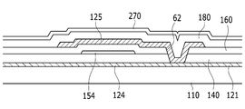
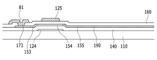
투명한 유리 또는 플라스틱 등으로 이루어진 기판(110) 위에 게이트선(121)이 위치하고 있다. 게이트선(121)는 게이트 신호를 전달하며 주로 가로 방향으로 뻗어 있다. 각 게이트선(121)은 아래쪽으로 돌출된 복수개의 하부 게이트 전극(bottom gate electrode)(124)를 포함한다. 또한, 게이트선(121)은 다른 층 또는 외부 구동 회로와의 접속을 위한 게이트 패드부(도시하지 않음)를 포함할 수 있다.A
이러한 게이트선(121)은 알루미늄(Al)이나 알루미늄 합금 등 알루미늄 계열 금속, 은(Ag)이나 은 합금 등 은 계열 금속, 구리(Cu)나 구리 합금 등 구리 계열 금속, 몰리브덴(Mo)이나 몰리브덴 합금 등 몰리브덴 계열 금속, 크롬(Cr), 탄탈륨(Ta) 및 티타늄(Ti) 따위로 만들어질 수 있다. 그러나 게이트선(121)은 물리적 성질이 다른 적어도 두 개의 도전막을 포함하는 다중막 구조를 가질 수도 있다. The
게이트선(121) 위에는 제1 절연막(140)이 형성되어 있다. 제1 절연막(140)은 10 atm% 내지 35 atm%의 불소 원자를 포함하고 있는 실리콘 질화막(P-SiNx:F)일 수 있다. 이러한 제1 절연막(140)의 두께는 50nm 내지 1000nm 이며, 바람직하게는 70nm 내지 700nm일 수 있다. A first insulating
하부 게이트 전극(124)을 덮는 제1 절연막(140)을 10 atm% 내지 35 atm%의 불소 원자를 포함하는 실리콘 질화막(P-SiNx:F)으로 형성함으로써, 유리로 이루어진 기판(110)에 포함된 알칼리 금속 이온의 전계 확산을 방지할 수 있고, 산화물 반도체의 문턱 전압의 이동을 최소화할 수 있어 박막 트랜지스터의 신뢰성을 높일 수 있다. The first
또한, 10 atm% 내지 35 atm%의 불소 원자를 포함하는 실리콘 질화막(P-SiNx:F)으로 형성된 제1 절연막(140)은 엑시머 레이저를 상당히 잘 투과시키므로, 엑시머 레이저를 이용한 산화물 반도체의 도체화 공정에서 하부 게이트 전극(124)에 의해 차단된 영역 이외의 영역을 선택적으로 고온 어닐링(annealing) 처리하는 것이 가능하다. 따라서, 산화물 반도체의 선택 영역에 고온 어닐링 공정을 진행하여 소스 전극, 채널, 드레인 전극 및 화소 전극을 형성할 수 있으므로 박막 트랜지스터를 단순한 구조로 간단하게 형성할 수 있다.In addition, since the first insulating
도 5는 본 발명의 일 실시예에 따른 액정 표시 장치의 제1 절연막의 투과율곡선(A)과, 종래의 액정 표시 장치의 제1 절연막의 투과율 곡선(B)을 도시한 그래프이다. 5 is a graph showing the transmittance curve (A) of the first insulating film of the liquid crystal display device and the transmittance curve (B) of the first insulating film of the conventional liquid crystal display device according to an embodiment of the present invention.
도 5에 도시한 바와 같이, 종래의 액정 표시 장치의 제1 절연막은 3종류의 원료 가스(SiH4 + NH3 + N2)를 혼합하여 성막한 실리콘 질화막(P-SiNx:H)으로서, 200nm의 두께로 형성된 경우, 실리콘 질화막의 308nm 파장의 광에 대한 투과율은 5% 정도로 상당히 작다. 그러나, 본 발명의 일 실시예에 따른 액정 표시 장치의 제1 절연막(140)은 불화규소(SiF4)와 질소(N2)의 혼합 가스를 CVD 장치에서 반응시켜 형성한 실리콘 질화막(P-SiNx:F)으로서, 200nm의 두께로 형성된 경우, 실리콘 질화막의 308nm 파장의 광에 대한 투과율은 94%로 상당히 높게 나타남을 알 수 있다.5, the first insulating film of a conventional liquid crystal display device is a silicon nitride film (P-SiNx: H) formed by mixing three kinds of source gases (SiH 4 + NH 3 + N 2 ) , The transmittance of the silicon nitride film with respect to light having a wavelength of 308 nm is as small as about 5%. However, the first insulating
또한, 실리콘 질화막(P-SiNx:F)의 두께가 400nm 인 경우에도 파장이 308㎚인 제논 크로라이드 엑시머 레이저의 광은 88% 이상 투과하므로 200J/㎠ 펄스의 광을 조사해도 막 벗겨짐은 발생하지 않는다. Further, even when the thickness of the silicon nitride film (P-SiNx: F) is 400 nm, the light of the Xenon Chloride excimer laser with a wavelength of 308 nm is transmitted by 88% or more, so even if light of 200 J / Do not.
제1 절연막(140) 위에는 활성 부재(150)와 화소 전극(190)이 형성되어 있다. 활성 부재(150)는 하부 게이트 전극(124)과 일부 중첩하고 있으며, 화소 전극(190)은 활성 부재(150)에서 연장되어 넓은 면적을 차지하며 형성되어 있다. 활성 부재(150)는 하부 게이트 전극(124)과 중첩하고 있는 채널(154), 채널(154)의 양 옆에 위치하고 있는 소스 전극(153) 및 드레인 전극(155)을 포함한다. 드레인 전극(155)은 채널(154)과 화소 전극(190) 사이에 위치하고 있다. 실질적으로 드레인 전극(155)은 경계선 없이 화소 전극(190)과 연속적으로 연결되어 있다. 이와 같이, 화소 전극(190)은 드레인 전극(155)과 동일한 물질로 동일한 층에 서로 연결되어 형성되므로 화소 전극(190)을 드레인 전극(155)과 연결하기 위한 별도의 접촉 구멍을 형성하지 않아도 되므로 개구율을 향상시킬 수 있다. An
이러한 활성 부재(150)와 화소 전극(190)은 산화물 반도체로 이루어져 있으며, 산화물 반도체는 티타늄(Ti), 하프늄(Hf), 지르코늄(Zr), 알루미늄(Al), 탄탈륨(Ta), 게르마늄(Ge), 아연(Zn), 갈륨(Ga), 주석(Sn) 또는 인듐(In)을 기본으로 하는 산화물, 이들의 복합 산화물인 인듐―갈륨―아연 산화물(InGaZnO4), 인듐―아연 산화물(Zn―In―O), 아연―주석 산화물(Zn―Sn―O) 인듐―갈륨 산화물 (In―Ga―O), 인듐―주석 산화물(In―Sn―O), 인듐―지르코늄 산화물(In―Zr―O), 인듐―지르코늄―아연 산화물(In―Zr―Zn―O), 인듐―지르코늄―주석 산화물(In―Zr―Sn―O), 인듐―지르코늄―갈륨 산화물(In―Zr―Ga―O), 인듐―알루미늄 산화물(In―Al―O), 인듐―아연―알루미늄 산화물(In―Zn―Al―O), 인듐―주석―알루미늄 산화물(In―Sn―Al―O), 인듐―알루미늄―갈륨 산화물(In―Al―Ga―O), 인듐―탄탈륨 산화물(In―Ta―O), 인듐―탄탈륨―아연 산화물(In―Ta―Zn―O), 인듐―탄탈륨―주석 산화물(In―Ta―Sn―O), 인듐―탄탈륨―갈륨 산화물(In―Ta―Ga―O), 인듐―게르마늄 산화물(In―Ge―O), 인듐―게르마늄―아연 산화물(In―Ge―Zn―O), 인듐―게르마늄―주석 산화물(In―Ge―Sn―O), 인듐―게르마늄―갈륨 산화물(In―Ge―Ga―O), 티타늄―인듐―아연 산화물(Ti―In―Zn―O), 하프늄―인듐―아연 산화물(Hf―In―Zn―O) 중 어느 하나를 포함할 수 있다. The active element 150 and the pixel electrode 190 are made of an oxide semiconductor and the oxide semiconductor is made of a metal such as titanium (Ti), hafnium (Hf), zirconium (Zr), aluminum (Al), tantalum (Ta), germanium Gallium-zinc oxide (InGaZnO4), indium-zinc oxide (Zn-In), indium-zinc oxide (Zn-In), or the like, which are oxides based on zinc (Zn), gallium (Ga), tin (In-Zr-O), indium-tin oxide (In-Sn-O), indium-zirconium oxide (In- Zirconium-zinc oxide (In-Zr-Zn-O), indium-zirconium-tin oxide (In-Zr-Sn-O), indium-zirconium-gallium oxide Aluminum oxide (In-Al-O), indium-zinc-aluminum oxide (In-Zn-Al-O), indium-tin- In-Al-Ga-O), Tantalum oxide (In-Ta-Sn-O), indium-tantalum-gallium oxide (In-Ta-Zn-O) (In-Ge-Zn-O), indium-germanium-tin oxide (In-Ge-Zn-O) In-Zn-O), indium-germanium-gallium oxide (In-Ge-Ga-O), titanium-indium-zinc oxide ). ≪ / RTI >
제1 절연막(140) 위에는 활성 부재(150)와 화소 전극(190)을 덮고 있는 제2 절연막(160)이 형성되어 있다. 제2 절연막(160)은 10 atm% 내지 35 atm%의 불소 원자를 포함하고 있는 실리콘 질화막(P-SiNx:F 또는 P-SiONx:F)일 수 있다. 이러한 제2 절연막(160)의 두께는 50nm 내지 1000nm 이며, 바람직하게는 70nm 내지 700nm일 수 있다. A second insulating
제2 절연막(160) 위에는 데이터선(171) 및 상부 게이트 전극(125)이 형성되어 있다. 데이터선(171)은 데이터 신호를 전달하며 주로 세로 방향으로 뻗어 게이트선(121)과 교차한다. 데이터선(171)에서 하부 게이트 전극(124)을 향하여 뻗은 돌출부(173)는 제2 절연막(160)에 형성된 접촉 구멍(183)을 통해 소스 전극(153)과 연결되어 있다. 데이터선(171)은 다른 층 또는 외부 구동 회로와의 접속을 위한 데이터 패드부(도시하지 않음)를 포함할 수 있다. A
상부 게이트 전극(125)은 채널(154) 및 하부 게이트 전극(124)과 중첩하고 있다. 그리고, 상부 게이트 전극(125)은 제1 절연막(140) 및 제2 절연막(160)에 함께 형성된 제2 접촉 구멍(62)을 통해 하부 게이트 전극(124)과 연결되어 있다. 따라서, 채널(154)의 상부 및 하부 양쪽에서 게이트 전압을 인가하는 더블 게이트 구조(Double Gate)를 적용함으로써, 채널(154) 내부의 전자 이동도를 향상시킬 수 있다. 또한, 상부 게이트 전극(125)을 불투명한 금속 물질로 형성하는 경우에는 산화물 반도체로 이루어진 채널(154)을 외부 광으로부터 차단할 수 있으므로 박막 트랜지스터의 신뢰성을 향상시킬 수 있다. 또한, 공통 전극(270)이 산화물 반도체로 이루어진 화소 전극(190)과 중첩하고 있으므로, 화소 전극(190)과 동일한 층에 형성되며 산화물 반도체로 이루어진 활성 부재(150)의 채널(154)은 공통 전극(270)의 전계의 영향을 받게 되나, 더블 게이트 구조에서는 공통 전극(270)의 전계를 상부 게이트 전극(125)으로 차단할 수 있으므로 오프 전류의 발생을 방지할 수 있다.The
또한, 상부 게이트 전극(125)의 폭(d2)은 하부 게이트 전극(124)의 폭(d1)보다 작을 수 있다. 그리고, 상부 게이트 전극(125)의 테두리는 대응하는 하부 게이트 전극(124)의 테두리 내측에 위치하고 있다. 따라서, 상부 게이트 전극(125)은 하부 게이트 전극(124)의 테두리 외측으로 돌출되어 있지 않다. 따라서, 상부 게이트 전극(125)은 모든 영역이 하부 게이트 전극(124)과 중첩하고 있으나, 하부 게이트 전극(124)은 상부 게이트 전극(125)과 중첩하지 않는 영역이 존재하게 된다. 따라서, 상부 게이트 전극(125)과 인접한 화소 전극(190) 간의 거리(d3)를 최대한 이격시킬 수 있으므로 상부 게이트 전극(125)과 화소 전극(190)간의 기생 용량을 최소화하여 박막 트랜지스터의 오프 시 킥백 전압(Kickback Voltage)을 최소화시킬 수 있어 잔상 발생을 억제할 수 있다.The
또한, 상부 게이트 전극(125)의 폭(d2)이 하부 게이트 전극(124)의 폭(d1)보다 작은 경우에는 데이터선(171)을 통해 소스 전극(153)과 화소 전극(190)에 30V~40V의 고전압이 인가되어도 상부 게이트 전극(125)과 인접한 화소 전극(190) 간의 거리(d3)를 최대한 이격되어 있으므로 박막 트랜지스터의 문턱 전압 이동(Vth shift)은 발생하기 어렵다. When the width d2 of the
하부 게이트 전극(124) 및 상부 게이트 전극(125)은 채널(154), 소스 전극(153) 및 드레인 전극(155)을 포함하는 활성 부재(150)와 함께 하나의 박막 트랜지스터(thin film transistor, TFT)를 이룬다. 따라서, 데이터선(171)으로부터 제1 접촉 구멍(61)을 통해 인가된 데이터 전압은 박막 트랜지스터(TFT)를 통해 화소 전극(190)으로 전달된다. The
데이터선(171) 및 상부 게이트 전극(125)은 몰리브덴, 크롬, 탄탈륨 및 티타늄 등 내화성 금속(refractory metal) 또는 이들의 합금으로 만들어지는 것이 바람직하며, 내화성 금속막(도시하지 않음)과 저저항 도전막(도시하지 않음)을 포함하는 다중막 구조를 가질 수 있다. 다중막 구조의 예로는 크롬 또는 몰리브덴 (합금) 하부막과 알루미늄 (합금) 상부막의 이중막, 몰리브덴 (합금) 하부막과 알루미늄 (합금) 중간막과 몰리브덴 (합금) 상부막의 삼중막을 들 수 있다. 그러나 데이터선(171)은 이외에도 여러 가지 다양한 금속 또는 도전체로 만들어질 수 있다.The
제2 절연막(160), 데이터선(171) 및 상부 게이트 전극(125) 위에는 이를 덮는 보호막(180)이 형성되어 있다. 보호막(180)은 화소 전극(190) 및 공통 전극(270)의 쇼트를 방지하기 위한 것으로서, 쇼트가 발생하지 않는 범위 내에서 최대한 얇게 형성될 수 있다. 이러한 보호막(180)은 유기 물질 또는 무기 물질로 이루어질 수 있다. A
보호막(180) 위에는 공통 전극(270)이 형성되어 있다. 공통 전극(270)은 공통 개구부(271)에 의해 복수개의 가지 공통 전극(272)으로 나누어지며, 복수개의 가지 공통 전극(272)은 화소 전극(190)과 중첩하고 있다. A
공통 전극(270)의 연장 방향은 데이터선(171)의 연장 방향 및 화소 전극(190)의 연장 방향과 서로 평행하게 배치되어 있다. 공통 전극(270)은 화소 전극(190)과 전기장을 형성하여 액정을 배향시킨다. 공통 전극(270)은 ITO(Indium Tin Oxide), IZO(Indium Zinc Oxide) 등을 포함하는 TCO와 같은 투명한 도전층으로 이루어질 수 있다. 본 실시예에서는 게이트선(121)의 연장 방향과 수직한 방향으로 연장된 공통 가지 전극을 도시하고 이를 기준으로 다른 구성요소를 설명하였으나, 이에 제한되지 않고 게이트선(121)의 연장 방향과 평행한 방향으로 연장된 공통 가지 전극으로 형성될 수 있다.The extending direction of the
공통 전극(270) 및 보호막(180) 위에는 배향막(11)이 도포되어 있고, 배향막(11)은 수평 배향막일 수 있으며, 일정한 방향으로 러빙되어 있다. An
그러면, 이하에서는 상부 표시판(200)에 대하여 설명한다.In the following, the
투명한 유리 또는 플라스틱 등으로 만들어진 기판(210) 위에 차광 부재(light blocking member)(220)가 형성되어 있다. 차광 부재(220)는 블랙 매트릭스(black matrix)라고도 하며 빛샘을 막아준다. 또한, 기판(210) 위에는 복수의 색필터(230)가 형성되어 있다. 색필터(230) 및 차광 부재(220) 위에는 덮개막(overcoat)(250)이 형성되어 있다. 덮개막(250)은 유기 물질로 만들어질 수 있으며, 색필터(230)가 노출되는 것을 방지하고 평탄면을 제공한다. 이러한 덮개막(250)은 생략할 수 있다. 덮개막(250) 위에는 배향막이 형성되어 있을 수 있다.A
하부 표시판(100)과 상부 표시판(200) 사이에 들어 있는 액정층(3)은 액정 분자(도시하지 않음)를 포함하며 액정 분자는 전기장이 없는 상태에서 그 장축이 두 표시판(100, 200)의 표면에 대하여 수평을 이루도록 배향되어 있을 수 있다.The
하부 표시판(100)의 기판(110)의 바깥쪽에는 빛을 생성하여 두 표시판(100, 200)에 빛을 제공하는 라이트 유닛(도시하지 않음)을 더 포함할 수 있다.The
데이터 전압이 인가된 화소 전극(190)은 공통 전압을 인가받는 공통 전극(270)과 함께 액정층(3)에 전기장을 생성함으로써 액정층(3)의 액정 분자의 방향을 결정하고 해당 영상을 표시한다.The
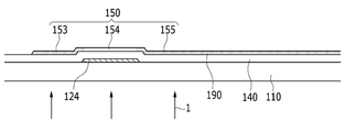
상기 본 발명의 일 실시예에 따른 액정 표시 장치의 제조 방법에 대해 이하에서 도 6 내지 도 12를 참고로 상세히 설명한다. A method of manufacturing a liquid crystal display device according to an embodiment of the present invention will be described in detail with reference to FIGS. 6 to 12. FIG.
도 6은 본 발명의 일 실시예에 따른 액정 표시 장치의 제조 방법의 순서도이고, 도 7, 9 및 11은 본 발명의 일 실시예에 따른 액정 표시 장치의 제조 방법을 순서대로 도시한 배치도이고, 도 8은 도 7의 액정 표시 장치를 VIII-VIII선을 따라 자른 단면도이고, 도 10은 도 9의 액정 표시 장치를 X-X선을 따라 자른 단면도이고, 도 12는 도 11의 액정 표시 장치를 XII-XII선을 따라 자른 단면도이다.7, 9, and 11 are views showing a method of fabricating a liquid crystal display according to an embodiment of the present invention, and FIG. 6 is a flow chart of a method of manufacturing a liquid crystal display device according to an embodiment of the present invention. FIG. 8 is a cross-sectional view taken along the line VIII-VIII of FIG. 7, FIG. 10 is a cross-sectional view of the liquid crystal display device of FIG. 9 taken along the line XX, Sectional view taken along the line XII.
우선, 도 6 내지 도 8에 도시한 바와 같이, 기판(110) 위에 하부 게이트 전극(124)을 포함하는 게이트선(121)을 형성한다(S10). 그리고, 그 위에 불화규소(SiF4)와 질소(N2)의 혼합 가스를 CVD 장치에서 반응시켜 형성한 실리콘 질화막(P-SiNx:F)으로 제1 절연막(140)을 형성한다(S20). First, as shown in FIGS. 6 to 8, a
그리고, 제1 절연막(140) 위에 산화물 반도체(50)를 형성한다(S30). Then, an
다음으로, 도 6, 도 9 및 도 10에 도시한 바와 같이, 하부 게이트 전극(124)을 차단 마스크로 하여 엑시머 레이저(1)를 기판(110) 아래에서 조사하여 산화물 반도체(50)에 활성 부재(150) 및 화소 전극(190)을 형성한다(S40). 활성 부재(150)는 하부 게이트 전극(124)과 중첩하여 엑시머 레이저(1)가 조사되지 않은 영역에는 채널(154)이 형성되고, 채널(154)의 양 옆의 영역에는 엑시머 레이저(1)가 조사되어 도체화됨으로써, 소스 전극(153) 및 드레인 전극(155)을 형성한다. 산화물 반도체(50) 중 드레인 전극(155)에 연결된 대부분의 영역에는 화소 전극(190)이 형성된다. Next, as shown in FIGS. 6, 9 and 10, the
다음으로, 도 6, 도 11 및 도 12에 도시한 바와 같이, 제1 절연막(140), 활성 부재(150) 및 화소 전극(190)을 덮는 제2 절연막(160)을 형성한다(S50). 제2 절연막(160)은 불화규소(SiF4)와 질소(N2)의 혼합 가스를 CVD 장치에서 반응시켜 실리콘 질화막(P-SiNx:F 또는 P-SiONx:F)으로 형성한다. 그리고, 제2 절연막(160)에 소스 전극(153)을 노출하는 제1 접촉 구멍(61)을 형성한다(S60). 그리고, 제2 절연막(160) 위에 데이터선(171) 및 상부 게이트 전극(125)을 형성한다(S70). Next, as shown in FIGS. 6, 11 and 12, a second
다음으로, 도 6, 도 1 내지 도 4에 도시한 바와 같이, 데이터선(171) 및 상부 게이트 전극(125)을 덮는 보호막(180)을 형성한다(S80). 보호막(180)은 불화규소(SiF4)와 질소(N2)의 혼합 가스를 CVD 장치에서 반응시켜 실리콘 질화막(P-SiNx:F)으로 형성한다. 그리고, 보호막(180)에 제2 접촉 구멍(62)을 형성한다(S90). Next, as shown in Fig. 6 and Fig. 1 to Fig. 4, a
그리고, 보호막(180) 위에 화소 전극(190)과 중첩하는 공통 전극(270)을 형성한다(S100). 그리고, 하부 표시판(100)에 배향막(11)을 형성한 후, 상부 표시판(200)과 하부 표시판(100) 사이에 액정층(3)을 주입하여 액정 표시 장치를 완성한다. A
한편, 상기 일 실시예에서는 공통 전극(270), 데이터선(171) 및 화소 전극(190)이 게이트선과 데이터선이 절연되어 교차하며 이루는 화소 영역 내에서 굴곡되어 있지 않으나, 데이터선, 화소 전극 및 공통 전극이 굴곡되어 있는 다른 실시예도 가능하다. Although the
이하에서 도 13 내지 도 15를 참고하여 다른 실시예에 대해 상세히 설명한다. Hereinafter, another embodiment will be described in detail with reference to FIG. 13 to FIG.
도 13은 본 발명의 다른 실시예에 따른 액정 표시 장치의 배치도이고, 도 14는 도 13의 C 부분의 확대도이고, 도 15는 도 13의 액정 표시 장치를 XV-XV선을 따라 잘라 도시한 단면도이다.13 is an arrangement view of a liquid crystal display device according to another embodiment of the present invention, Fig. 14 is an enlarged view of a portion C in Fig. 13, Fig. 15 is a cross-sectional view taken along line XV- Sectional view.
도 13 내지 도 15에 도시된 다른 실시예는 도 1 내지 도 4에 도시된 일 실시예와 비교하여 공통 전극, 데이터선 및 화소 전극이 굴곡되고, 상부 게이트 전극의 테두리는 대응하는 하부 게이트 전극의 테두리 외측에 위치하고 있는 것만을 제외하고 실질적으로 동일한 바 반복되는 설명은 생략한다.13 to 15, the common electrode, the data line, and the pixel electrode are bent as compared with the embodiment shown in FIGS. 1 to 4, and the rim of the upper gate electrode is bent Substantially the same repetitive description will be omitted except that it is located outside the frame.
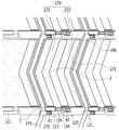
도 13 내지 도 15에 도시한 바와 같이, 본 발명의 다른 실시예에 따른 액정 표시 장치는 투과율을 향상시키기 위해 데이터선(171), 화소 전극(191) 및 공통 전극(270)의 공통 가지 전극(272)은 굽어진 형상을 갖는 굴곡부(2)를 가지고 있다. 이러한 굴곡부는 화소 영역의 중간 영역에서 V자 형태를 이룰 수 있다. 그러나 데이터선(171), 화소 전극(191) 및 공통 전극(270)의 형상은 전술한 형상에 제한되지 않으며 어떠한 형상도 가질 수 있다. 13 to 15, a liquid crystal display device according to another embodiment of the present invention includes a
그리고, 도 14에 도시한 바와 같이, 하부 게이트 전극(124)의 테두리 중 화소 전극(190)에 가장 가까이 인접하고 있는 제1 테두리(21)는 상부 게이트 전극(125)의 테두리 중 화소 전극(190)에 가장 가까이 인접하고 있는 제2 테두리(22)보다 화소 전극(190)에 더 인접하게 배치되어 있다. 따라서, 상부 게이트 전극(125)과 화소 전극(190)간의 간격(d3)를 넓혀 상부 게이트 전극(125)과 화소 전극(190)간에 형성되는 기생 용량을 최소화하여 킥백 전압 및 이에 따른 잔상 발생을 최소화할 수 있다.14, the
이 때, 하부 게이트 전극(124)의 테두리 중 제1 테두리(21) 맞은 편의 제3 테두리(23)는 상부 게이트 전극(125)의 테두리 중 제2 테두리(22) 맞은 편의 제4 테두리(24)의 외측에 위치하게 된다. A
본 발명을 앞서 기재한 바에 따라 바람직한 실시예를 통해 설명하였지만, 본 발명은 이에 한정되지 않으며 다음에 기재하는 특허청구범위의 개념과 범위를 벗어나지 않는 한, 다양한 수정 및 변형이 가능하다는 것을 본 발명이 속하는 기술 분야에 종사하는 자들은 쉽게 이해할 것이다.While the invention has been shown and described with reference to certain preferred embodiments thereof, it will be understood by those skilled in the art that various changes and modifications may be made therein without departing from the spirit and scope of the following claims. Those who are engaged in the technology field will understand easily.
121: 게이트선
124: 하부 게이트 전극
125: 상부 게이트 전극
140: 제1 절연막
150: 활성 부재
153: 소스 전극
154: 채널
155: 드레인 전극
160: 제2 절연막
171: 데이터선
180: 보호막
190: 화소 전극
270: 공통 전극
271: 공통 개구부
272: 가지 공통 전극121: gate line 124: bottom gate electrode
125: upper gate electrode 140: first insulating film
150: active member 153: source electrode
154: channel 155: drain electrode
160: second insulating film 171: data line
180: protective film 190: pixel electrode
270: common electrode 271: common opening
272: branch common electrode
Claims (16)
상기 기판 위에 형성되어 있으며 하부 게이트 전극을 포함하는 게이트선,
상기 게이트선을 덮고 있는 제1 절연막,
상기 제1 절연막 위에 형성되어 있으며 상기 하부 게이트 전극과 중첩하고 있는 채널, 상기 채널 양 옆에 위치하고 있는 소스 전극 및 드레인 전극을 포함하는 활성 부재,
상기 활성 부재와 동일한 층에 형성되어 있는 화소 전극,
상기 활성 부재 및 화소 전극을 덮고 있는 제2 절연막,
상기 제2 절연막 위에 형성되어 있으며 상기 활성 부재와 연결되어 있는 데이터선,
상기 데이터선을 덮고 있는 보호막,
상기 보호막 위에 형성되어 있으며 상기 화소 전극과 중첩하고 있는 공통 전극
을 포함하고,
상기 활성 부재와 화소 전극은 산화물 반도체로 이루어져 있는 액정 표시 장치.Board,
A gate line formed on the substrate and including a lower gate electrode,
A first insulating film covering the gate line,
An active member formed on the first insulating film and including a channel overlapping the lower gate electrode, source and drain electrodes located on both sides of the channel,
A pixel electrode formed on the same layer as the active member,
A second insulating film covering the active element and the pixel electrode,
A data line formed on the second insulating film and connected to the active member,
A protective film covering the data line,
A common electrode formed on the protective film and overlapping the pixel electrode,
/ RTI >
Wherein the active member and the pixel electrode are made of an oxide semiconductor.
상기 제1 절연막은 10 atm% 내지 35 atm%의 불소 원자를 포함하고 있는 실리콘 질화막인 액정 표시 장치.The method of claim 1,
Wherein the first insulating film is a silicon nitride film containing 10 atom% to 35 atom% of fluorine atoms.
상기 제2 절연막 위에 형성되어 있으며 상기 하부 게이트 전극과 중첩하고 있는 상부 게이트 전극을 더 포함하는 액정 표시 장치. The method of claim 1,
And a top gate electrode formed on the second insulating film and overlapped with the bottom gate electrode.
상기 상부 게이트 전극의 폭은 상기 하부 게이트 전극의 폭보다 작은 액정 표시 장치.4. The method of claim 3,
Wherein a width of the upper gate electrode is smaller than a width of the lower gate electrode.
상기 상부 게이트 전극의 테두리는 대응하는 상기 하부 게이트 전극의 테두리 내측에 위치하고 있는 액정 표시 장치. 5. The method of claim 4,
And the rim of the upper gate electrode is located inside the rim of the corresponding lower gate electrode.
상기 하부 게이트 전극의 테두리 중 상기 화소 전극에 가장 가까이 인접하고 있는 제1 테두리는 상기 상부 게이트 전극의 테두리 중 상기 화소 전극에 가장 가까이 인접하고 있는 제2 테두리보다 상기 화소 전극에 더 인접하고 있는 액정 표시 장치. 4. The method of claim 3,
Wherein a first edge of the rim of the lower gate electrode closest to the pixel electrode is closer to the pixel electrode than a second rim of the rim of the upper gate electrode that is closest to the pixel electrode, Device.
상기 데이터선은 상기 제1 절연막에 형성된 제1 접촉 구멍을 통해 상기 활성 부재와 연결되어 있고, 상기 상부 게이트 전극은 상기 제1 절연막 및 제2 절연막에 함께 형성된 제2 접촉 구멍을 통해 상기 하부 게이트 전극과 연결되어 있는 액정 표시 장치.The method of claim 1,
Wherein the data line is connected to the active member through a first contact hole formed in the first insulating film and the upper gate electrode is connected to the lower gate electrode through a second contact hole formed in the first insulating film and the second insulating film, And the liquid crystal display device.
상기 제2 절연막은 10 atm% 내지 35 atm%의 불소 원자를 포함하고 있는 실리콘 질화막인 액정 표시 장치.The method of claim 1,
Wherein the second insulating film is a silicon nitride film containing 10 atom% to 35 atom% of fluorine atoms.
상기 제1 절연막의 두께는 50nm 내지 1000nm 이고, 상기 제2 절연막의 두께는 50nm 내지 1000nm 인 액정 표시 장치.9. The method of claim 8,
The thickness of the first insulating film is 50 nm to 1000 nm, and the thickness of the second insulating film is 50 nm to 1000 nm.
상기 데이터선의 연장 방향, 상기 화소 전극의 연장 방향 및 상기 공통 전극의 연장 방향은 서로 평행하게 배치되어 있는 액정 표시 장치.The method of claim 1,
Wherein the extending direction of the data line, the extending direction of the pixel electrode, and the extending direction of the common electrode are arranged parallel to each other.
상기 게이트선과 상기 데이터선이 절연되어 교차하며 이루는 화소 영역 내에서 상기 데이터선, 상기 화소 전극 및 상기 공통 전극은 굴곡되어 있는 액정 표시 장치.11. The method of claim 10,
Wherein the data line, the pixel electrode, and the common electrode are bent in a pixel region where the gate line and the data line are insulated and crossed.
상기 하부 게이트 전극과 상기 데이터선의 사이각은 70도 내지 89도 인 액정 표시 장치. 12. The method of claim 11,
And the angle between the lower gate electrode and the data line is 70 degrees to 89 degrees.
상기 게이트선을 덮으며 10 atm% 내지 35 atm%의 불소 원자를 포함하는 실리콘 질화막으로 제1 절연막을 형성하는 단계,
상기 제1 절연막 위에 산화물 반도체를 형성하는 단계,
상기 하부 게이트 전극을 차단 마스크로 하여 엑시머 레이저를 조사하여 상기 산화물 반도체에 활성 부재 및 화소 전극을 형성하는 단계,
상기 활성 부재 및 화소 전극을 덮는 제2 절연막을 형성하는 단계,
상기 제2 절연막 위에 상기 게이트선과 교차하는 데이터선을 형성하는 단계,
상기 데이터선을 덮는 보호막을 형성하는 단계,
상기 보호막 위에 상기 화소 전극과 중첩하는 공통 전극을 형성하는 단계
를 포함하는 액정 표시 장치의 제조 방법.Forming a gate line including a lower gate electrode on a substrate,
Forming a first insulating film covering the gate line with a silicon nitride film containing 10 atom% to 35 at% of fluorine atoms,
Forming an oxide semiconductor on the first insulating film,
Forming an active material and a pixel electrode on the oxide semiconductor by irradiating an excimer laser using the lower gate electrode as a blocking mask,
Forming a second insulating film covering the active member and the pixel electrode,
Forming a data line crossing the gate line on the second insulating film;
Forming a protective film covering the data line,
Forming a common electrode overlapping the pixel electrode on the passivation layer
And the second electrode is electrically connected to the second electrode.
상기 데이터선을 형성하는 단계에서 상기 하부 게이트 전극과 중첩하는 상부 게이트 전극을 형성하는 액정 표시 장치의 제조 방법.The method of claim 13,
And forming an upper gate electrode overlapping the lower gate electrode in the step of forming the data line.
상기 제2 절연막은 10 atm% 내지 35 atm%의 불소 원자를 포함하는 실리콘 질화막으로 형성하는 액정 표시 장치의 제조 방법.The method of claim 13,
Wherein the second insulating film is formed of a silicon nitride film containing 10 atom% to 35 atom% of fluorine atoms.
상기 제1 절연막 및 제2 절연막은 불화규소(SiF4)와 질소(N2)의 혼합 가스를 CVD 장치에서 반응시켜 형성하는 액정 표시 장치의 제조 방법.16. The method of claim 15,
Wherein the first insulating film and the second insulating film are formed by reacting a mixed gas of silicon fluoride (SiF 4 ) and nitrogen (N 2 ) in a CVD apparatus.
Priority Applications (2)
| Application Number | Priority Date | Filing Date | Title |
|---|---|---|---|
| KR1020140137545A KR20160043576A (en) | 2014-10-13 | 2014-10-13 | Liquid crystal display and manufacturing method thereof |
| US14/692,893 US9331103B1 (en) | 2014-10-13 | 2015-04-22 | Liquid crystal display and manufacturing method thereof |
Applications Claiming Priority (1)
| Application Number | Priority Date | Filing Date | Title |
|---|---|---|---|
| KR1020140137545A KR20160043576A (en) | 2014-10-13 | 2014-10-13 | Liquid crystal display and manufacturing method thereof |
Publications (1)
| Publication Number | Publication Date |
|---|---|
| KR20160043576A true KR20160043576A (en) | 2016-04-22 |
Family
ID=55655996
Family Applications (1)
| Application Number | Title | Priority Date | Filing Date |
|---|---|---|---|
| KR1020140137545A KR20160043576A (en) | 2014-10-13 | 2014-10-13 | Liquid crystal display and manufacturing method thereof |
Country Status (2)
| Country | Link |
|---|---|
| US (1) | US9331103B1 (en) |
| KR (1) | KR20160043576A (en) |
Families Citing this family (5)
| Publication number | Priority date | Publication date | Assignee | Title |
|---|---|---|---|---|
| JP2016225615A (en) * | 2015-05-26 | 2016-12-28 | 株式会社半導体エネルギー研究所 | Semiconductor device, semiconductor device manufacturing method and display device having semiconductor device |
| CN104900531A (en) * | 2015-06-08 | 2015-09-09 | 京东方科技集团股份有限公司 | Oxide thin-film transistor and array substrate, and manufacturing methods thereof, and display apparatus |
| CN107248393B (en) * | 2017-07-24 | 2019-04-26 | 上海交通大学 | Pixel drive unit and forming method thereof, display backboard, pixel-driving circuit |
| US11342362B2 (en) * | 2018-03-30 | 2022-05-24 | Sharp Kabushiki Kaisha | Display device |
| TWI820861B (en) * | 2018-08-01 | 2023-11-01 | 日本商出光興產股份有限公司 | Crystal structure compounds, oxide sintered bodies, sputtering targets, crystalline oxide films, amorphous oxide films, thin film transistors, and electronic devices |
Family Cites Families (13)
| Publication number | Priority date | Publication date | Assignee | Title |
|---|---|---|---|---|
| US20010055074A1 (en) | 1997-07-22 | 2001-12-27 | Hiroshi Komatsu | In-plane switching mode lcd with specific arrangement of common bus line, data electrode, and common electrode |
| US6717181B2 (en) | 2001-02-22 | 2004-04-06 | Semiconductor Energy Laboratory Co., Ltd. | Luminescent device having thin film transistor |
| JP4809544B2 (en) | 2001-05-22 | 2011-11-09 | 株式会社半導体エネルギー研究所 | Light emitting device |
| EP1770788A3 (en) | 2005-09-29 | 2011-09-21 | Semiconductor Energy Laboratory Co., Ltd. | Semiconductor device having oxide semiconductor layer and manufacturing method thereof |
| KR101412761B1 (en) | 2008-01-18 | 2014-07-02 | 삼성디스플레이 주식회사 | Thin film transistor array substrate and method of fabricating the same |
| JP5602450B2 (en) | 2010-02-12 | 2014-10-08 | 三菱電機株式会社 | THIN FILM TRANSISTOR, MANUFACTURING METHOD THEREOF, AND DISPLAY DEVICE |
| JP5576814B2 (en) | 2011-02-25 | 2014-08-20 | 日本放送協会 | Semiconductor device and manufacturing method thereof |
| KR101941439B1 (en) | 2011-10-04 | 2019-01-24 | 엘지디스플레이 주식회사 | Oxide Thin Film Transistor Array Substrate and the method of manufacturing the same |
| JP5984354B2 (en) | 2011-10-07 | 2016-09-06 | 住友電気工業株式会社 | Semiconductor element |
| KR101960533B1 (en) | 2011-11-10 | 2019-03-21 | 엘지디스플레이 주식회사 | Thin Film Transistor Substrate Having Metal Oxide Semiconductor and Manufacturing Method Thereof |
| KR101952940B1 (en) | 2012-03-20 | 2019-05-29 | 삼성디스플레이 주식회사 | Electro phoresis display device |
| KR101985246B1 (en) * | 2012-07-06 | 2019-06-03 | 엘지디스플레이 주식회사 | Thin film transistor substrate having metal oxide and manufacturing method thereof |
| CN103456742B (en) * | 2013-08-27 | 2017-02-15 | 京东方科技集团股份有限公司 | Array substrate, manufacturing method of array substrate and display device |
-
2014
- 2014-10-13 KR KR1020140137545A patent/KR20160043576A/en not_active Application Discontinuation
-
2015
- 2015-04-22 US US14/692,893 patent/US9331103B1/en active Active
Also Published As
| Publication number | Publication date |
|---|---|
| US9331103B1 (en) | 2016-05-03 |
| US20160104723A1 (en) | 2016-04-14 |
Similar Documents
| Publication | Publication Date | Title |
|---|---|---|
| US11921392B2 (en) | Display device | |
| US11003012B2 (en) | Liquid crystal display device and manufacturing method thereof | |
| US20180122835A1 (en) | Display device | |
| KR101497425B1 (en) | Liquid crystal display and method of manufacturing the same | |
| KR102380647B1 (en) | Thin film transistor array panel and manufacturing method thereof | |
| KR102007833B1 (en) | Array substrate for fringe field switching mode liquid crystal display device | |
| KR102295477B1 (en) | Thin film transistor array panel | |
| KR101555113B1 (en) | Semiconductor device and process of producing same, and display device | |
| KR101323412B1 (en) | Liquid crystal display device and manufacturing method of the same | |
| KR101569766B1 (en) | Thin film transistor array panel and method for manufacturing the same | |
| TW200424974A (en) | Liquid crystal display device | |
| KR20160043576A (en) | Liquid crystal display and manufacturing method thereof | |
| US9620524B2 (en) | Array substrate and manufacturing method thereof, display device | |
| KR20170026219A (en) | Display device | |
| US20180277661A1 (en) | Thin film transistor substrate, manufacturing method for thin film transistor substrate, and liquid crystal display | |
| US10438977B2 (en) | Display device | |
| KR101987985B1 (en) | Thin film transistor array panel and method for manufacturing the same | |
| US10522567B2 (en) | Semiconductor device and display device having a protection layer | |
| KR20160128518A (en) | Display device and manufacturing method thereof | |
| KR20160120394A (en) | Thin film transistor array panel and method for manufacturing the same | |
| KR20160093178A (en) | Display device | |
| JP5090133B2 (en) | Liquid crystal display | |
| US9929186B2 (en) | Thin film transistor substrate and method for manufacturing the same | |
| KR102329294B1 (en) | Thin film transistor array panel and manufacturing method thereof | |
| KR20140001634A (en) | Array substrate, display panel having the same and method of manufacturing the same |
Legal Events
| Date | Code | Title | Description |
|---|---|---|---|
| WITN | Application deemed withdrawn, e.g. because no request for examination was filed or no examination fee was paid |