KR20150131090A - Metal oxide semiconductor (mos) isolation schemes with continuous active areas separated by dummy gates and related methods - Google Patents
Metal oxide semiconductor (mos) isolation schemes with continuous active areas separated by dummy gates and related methods Download PDFInfo
- Publication number
- KR20150131090A KR20150131090A KR1020157027562A KR20157027562A KR20150131090A KR 20150131090 A KR20150131090 A KR 20150131090A KR 1020157027562 A KR1020157027562 A KR 1020157027562A KR 20157027562 A KR20157027562 A KR 20157027562A KR 20150131090 A KR20150131090 A KR 20150131090A
- Authority
- KR
- South Korea
- Prior art keywords
- gate
- work function
- mos
- metal
- forming
- Prior art date
Links
- 238000002955 isolation Methods 0.000 title claims abstract description 39
- 239000004065 semiconductor Substances 0.000 title claims abstract description 15
- 229910044991 metal oxide Inorganic materials 0.000 title claims abstract description 11
- 150000004706 metal oxides Chemical class 0.000 title claims abstract description 11
- 238000000034 method Methods 0.000 title claims description 45
- 239000000463 material Substances 0.000 claims abstract description 58
- 239000002184 metal Substances 0.000 claims abstract description 54
- 238000009413 insulation Methods 0.000 claims description 10
- 238000002347 injection Methods 0.000 claims description 8
- 239000007924 injection Substances 0.000 claims description 8
- 230000005669 field effect Effects 0.000 claims description 4
- 238000004891 communication Methods 0.000 claims description 3
- 230000000295 complement effect Effects 0.000 claims description 3
- 230000001413 cellular effect Effects 0.000 claims description 2
- 238000002513 implantation Methods 0.000 claims 1
- 239000007769 metal material Substances 0.000 abstract description 5
- 230000006870 function Effects 0.000 description 52
- 239000000758 substrate Substances 0.000 description 9
- XUIMIQQOPSSXEZ-UHFFFAOYSA-N Silicon Chemical group [Si] XUIMIQQOPSSXEZ-UHFFFAOYSA-N 0.000 description 7
- 238000012545 processing Methods 0.000 description 7
- 229910052710 silicon Inorganic materials 0.000 description 7
- 239000010703 silicon Substances 0.000 description 7
- 238000013461 design Methods 0.000 description 6
- 238000013459 approach Methods 0.000 description 5
- 230000007246 mechanism Effects 0.000 description 5
- 230000008569 process Effects 0.000 description 5
- 238000005516 engineering process Methods 0.000 description 3
- 239000000243 solution Substances 0.000 description 3
- 238000010586 diagram Methods 0.000 description 2
- 230000006872 improvement Effects 0.000 description 2
- 230000001939 inductive effect Effects 0.000 description 2
- 238000004519 manufacturing process Methods 0.000 description 2
- 238000010295 mobile communication Methods 0.000 description 2
- 125000006850 spacer group Chemical group 0.000 description 2
- 230000008901 benefit Effects 0.000 description 1
- 230000015572 biosynthetic process Effects 0.000 description 1
- 230000015556 catabolic process Effects 0.000 description 1
- 230000008859 change Effects 0.000 description 1
- 238000007796 conventional method Methods 0.000 description 1
- 230000007547 defect Effects 0.000 description 1
- 238000006731 degradation reaction Methods 0.000 description 1
- 239000003989 dielectric material Substances 0.000 description 1
- 239000002019 doping agent Substances 0.000 description 1
- 230000008030 elimination Effects 0.000 description 1
- 238000003379 elimination reaction Methods 0.000 description 1
- 239000004744 fabric Substances 0.000 description 1
- 239000012212 insulator Substances 0.000 description 1
- 239000004973 liquid crystal related substance Substances 0.000 description 1
- 239000006249 magnetic particle Substances 0.000 description 1
- 238000012986 modification Methods 0.000 description 1
- 230000004048 modification Effects 0.000 description 1
- 239000002245 particle Substances 0.000 description 1
- 230000002085 persistent effect Effects 0.000 description 1
- 230000009467 reduction Effects 0.000 description 1
- 238000012360 testing method Methods 0.000 description 1
- 230000000007 visual effect Effects 0.000 description 1
Images


Classifications
-
- H—ELECTRICITY
- H01—ELECTRIC ELEMENTS
- H01L—SEMICONDUCTOR DEVICES NOT COVERED BY CLASS H10
- H01L29/00—Semiconductor devices adapted for rectifying, amplifying, oscillating or switching, or capacitors or resistors with at least one potential-jump barrier or surface barrier, e.g. PN junction depletion layer or carrier concentration layer; Details of semiconductor bodies or of electrodes thereof ; Multistep manufacturing processes therefor
- H01L29/66—Types of semiconductor device ; Multistep manufacturing processes therefor
- H01L29/66007—Multistep manufacturing processes
- H01L29/66075—Multistep manufacturing processes of devices having semiconductor bodies comprising group 14 or group 13/15 materials
- H01L29/66227—Multistep manufacturing processes of devices having semiconductor bodies comprising group 14 or group 13/15 materials the devices being controllable only by the electric current supplied or the electric potential applied, to an electrode which does not carry the current to be rectified, amplified or switched, e.g. three-terminal devices
- H01L29/66409—Unipolar field-effect transistors
- H01L29/66477—Unipolar field-effect transistors with an insulated gate, i.e. MISFET
- H01L29/66787—Unipolar field-effect transistors with an insulated gate, i.e. MISFET with a gate at the side of the channel
- H01L29/66795—Unipolar field-effect transistors with an insulated gate, i.e. MISFET with a gate at the side of the channel with a horizontal current flow in a vertical sidewall of a semiconductor body, e.g. FinFET, MuGFET
- H01L29/6681—Unipolar field-effect transistors with an insulated gate, i.e. MISFET with a gate at the side of the channel with a horizontal current flow in a vertical sidewall of a semiconductor body, e.g. FinFET, MuGFET using dummy structures having essentially the same shape as the semiconductor body, e.g. to provide stability
-
- H—ELECTRICITY
- H01—ELECTRIC ELEMENTS
- H01L—SEMICONDUCTOR DEVICES NOT COVERED BY CLASS H10
- H01L21/00—Processes or apparatus adapted for the manufacture or treatment of semiconductor or solid state devices or of parts thereof
- H01L21/70—Manufacture or treatment of devices consisting of a plurality of solid state components formed in or on a common substrate or of parts thereof; Manufacture of integrated circuit devices or of parts thereof
- H01L21/71—Manufacture of specific parts of devices defined in group H01L21/70
- H01L21/76—Making of isolation regions between components
- H01L21/762—Dielectric regions, e.g. EPIC dielectric isolation, LOCOS; Trench refilling techniques, SOI technology, use of channel stoppers
- H01L21/7624—Dielectric regions, e.g. EPIC dielectric isolation, LOCOS; Trench refilling techniques, SOI technology, use of channel stoppers using semiconductor on insulator [SOI] technology
-
- H—ELECTRICITY
- H01—ELECTRIC ELEMENTS
- H01L—SEMICONDUCTOR DEVICES NOT COVERED BY CLASS H10
- H01L21/00—Processes or apparatus adapted for the manufacture or treatment of semiconductor or solid state devices or of parts thereof
- H01L21/70—Manufacture or treatment of devices consisting of a plurality of solid state components formed in or on a common substrate or of parts thereof; Manufacture of integrated circuit devices or of parts thereof
- H01L21/71—Manufacture of specific parts of devices defined in group H01L21/70
- H01L21/76—Making of isolation regions between components
- H01L21/765—Making of isolation regions between components by field effect
-
- H—ELECTRICITY
- H01—ELECTRIC ELEMENTS
- H01L—SEMICONDUCTOR DEVICES NOT COVERED BY CLASS H10
- H01L21/00—Processes or apparatus adapted for the manufacture or treatment of semiconductor or solid state devices or of parts thereof
- H01L21/70—Manufacture or treatment of devices consisting of a plurality of solid state components formed in or on a common substrate or of parts thereof; Manufacture of integrated circuit devices or of parts thereof
- H01L21/77—Manufacture or treatment of devices consisting of a plurality of solid state components or integrated circuits formed in, or on, a common substrate
- H01L21/78—Manufacture or treatment of devices consisting of a plurality of solid state components or integrated circuits formed in, or on, a common substrate with subsequent division of the substrate into plural individual devices
- H01L21/82—Manufacture or treatment of devices consisting of a plurality of solid state components or integrated circuits formed in, or on, a common substrate with subsequent division of the substrate into plural individual devices to produce devices, e.g. integrated circuits, each consisting of a plurality of components
- H01L21/822—Manufacture or treatment of devices consisting of a plurality of solid state components or integrated circuits formed in, or on, a common substrate with subsequent division of the substrate into plural individual devices to produce devices, e.g. integrated circuits, each consisting of a plurality of components the substrate being a semiconductor, using silicon technology
- H01L21/8232—Field-effect technology
- H01L21/8234—MIS technology, i.e. integration processes of field effect transistors of the conductor-insulator-semiconductor type
- H01L21/8238—Complementary field-effect transistors, e.g. CMOS
- H01L21/823878—Complementary field-effect transistors, e.g. CMOS isolation region manufacturing related aspects, e.g. to avoid interaction of isolation region with adjacent structure
-
- H—ELECTRICITY
- H01—ELECTRIC ELEMENTS
- H01L—SEMICONDUCTOR DEVICES NOT COVERED BY CLASS H10
- H01L27/00—Devices consisting of a plurality of semiconductor or other solid-state components formed in or on a common substrate
- H01L27/02—Devices consisting of a plurality of semiconductor or other solid-state components formed in or on a common substrate including semiconductor components specially adapted for rectifying, oscillating, amplifying or switching and having at least one potential-jump barrier or surface barrier; including integrated passive circuit elements with at least one potential-jump barrier or surface barrier
- H01L27/0203—Particular design considerations for integrated circuits
- H01L27/0207—Geometrical layout of the components, e.g. computer aided design; custom LSI, semi-custom LSI, standard cell technique
-
- H—ELECTRICITY
- H01—ELECTRIC ELEMENTS
- H01L—SEMICONDUCTOR DEVICES NOT COVERED BY CLASS H10
- H01L29/00—Semiconductor devices adapted for rectifying, amplifying, oscillating or switching, or capacitors or resistors with at least one potential-jump barrier or surface barrier, e.g. PN junction depletion layer or carrier concentration layer; Details of semiconductor bodies or of electrodes thereof ; Multistep manufacturing processes therefor
- H01L29/66—Types of semiconductor device ; Multistep manufacturing processes therefor
- H01L29/68—Types of semiconductor device ; Multistep manufacturing processes therefor controllable by only the electric current supplied, or only the electric potential applied, to an electrode which does not carry the current to be rectified, amplified or switched
- H01L29/76—Unipolar devices, e.g. field effect transistors
- H01L29/772—Field effect transistors
- H01L29/78—Field effect transistors with field effect produced by an insulated gate
- H01L29/785—Field effect transistors with field effect produced by an insulated gate having a channel with a horizontal current flow in a vertical sidewall of a semiconductor body, e.g. FinFET, MuGFET
-
- H—ELECTRICITY
- H01—ELECTRIC ELEMENTS
- H01L—SEMICONDUCTOR DEVICES NOT COVERED BY CLASS H10
- H01L21/00—Processes or apparatus adapted for the manufacture or treatment of semiconductor or solid state devices or of parts thereof
- H01L21/70—Manufacture or treatment of devices consisting of a plurality of solid state components formed in or on a common substrate or of parts thereof; Manufacture of integrated circuit devices or of parts thereof
- H01L21/77—Manufacture or treatment of devices consisting of a plurality of solid state components or integrated circuits formed in, or on, a common substrate
- H01L21/78—Manufacture or treatment of devices consisting of a plurality of solid state components or integrated circuits formed in, or on, a common substrate with subsequent division of the substrate into plural individual devices
- H01L21/82—Manufacture or treatment of devices consisting of a plurality of solid state components or integrated circuits formed in, or on, a common substrate with subsequent division of the substrate into plural individual devices to produce devices, e.g. integrated circuits, each consisting of a plurality of components
- H01L21/822—Manufacture or treatment of devices consisting of a plurality of solid state components or integrated circuits formed in, or on, a common substrate with subsequent division of the substrate into plural individual devices to produce devices, e.g. integrated circuits, each consisting of a plurality of components the substrate being a semiconductor, using silicon technology
- H01L21/8232—Field-effect technology
- H01L21/8234—MIS technology, i.e. integration processes of field effect transistors of the conductor-insulator-semiconductor type
- H01L21/8238—Complementary field-effect transistors, e.g. CMOS
- H01L21/823828—Complementary field-effect transistors, e.g. CMOS with a particular manufacturing method of the gate conductors, e.g. particular materials, shapes
- H01L21/823842—Complementary field-effect transistors, e.g. CMOS with a particular manufacturing method of the gate conductors, e.g. particular materials, shapes gate conductors with different gate conductor materials or different gate conductor implants, e.g. dual gate structures
Abstract
상세한 설명에 개시된 실시예들은 더미게이트들에 의해 분리되는 연속 액티브 영역들을 이용한 MOS(metal oxide semiconductor) 절연 방식들을 포함한다. MOS 디바이스는 n-금속 또는 p-금속으로 설명되는 일함수를 갖는 물질로 형성되는 액티브 영역을 포함한다. 액티브 컴포넌트들은 유사한 일함수를 갖는 물질들을 이용하여 이 액티브 영역상에 형성된다. 액티브 컴포넌트들 사이에 더미 게이트를 포지셔닝함으로써 절연이 달성된다. 더미 게이트는 액티브 영역의 물질과 관련하여 상반되는 일함수를 갖는 물질로 만들어진다. 예를 들어, 액티브 영역이 p-금속 물질이었다면, 더미 게이트는 n-금속으로 만들어졌을 것이고, 액티브 영역이 n-금속 물질이었다면, 더미 게이트는 p-금속으로 만들어졌을 것이다 The embodiments disclosed in the detailed description include metal oxide semiconductor (MOS) isolation schemes using consecutive active regions separated by dummy gates. A MOS device includes an active region formed of a material having a work function, which is described as n-metal or p-metal. The active components are formed on the active region using materials having a similar work function. Isolation is achieved by positioning the dummy gate between the active components. The dummy gate is made of a material having an opposite work function with respect to the material of the active region. For example, if the active region was a p-metal material, the dummy gate would have been made of n-metal, and if the active region was an n-metal material, the dummy gate would have been made of p-
Description
[0001] 본 출원은 "METAL OXIDE SEMICONDUCTOR (MOS) ISOLATION SCHEMES WITH CONTINUOUS ACTIVE AREAS SEPARATED BY DUMMY GATES AND RELATED METHODS"란 명칭으로 2013년 3월 13일자로 출원된 미국 특허 출원 일련번호 13/799,955를 우선권으로 주장하며, 이는 전체 인용에 의해 본원에 포함된다.This application claims priority to United States Patent Application Serial No. 13 / 799,955, filed March 13, 2013, entitled METAL OXIDE SEMICONDUCTOR (MOS) ISOLATION SCHEMES WITH CONTINUOUS ACTIVE AREAS SEPARATED BY DUMMY GATES AND RELATED METHODS Which is hereby incorporated by reference in its entirety.
[0002] 본 개시물의 기술은 금속 산화물 반도체(MOS)에 관한 것이다. [0002] The present disclosure relates to metal oxide semiconductors (MOSs).
[0003] 모바일 통신 디바이스들은 현재 사회에서 보편화되었다. 이들 모바일 디바이스들의 보급은 이러한 디바이스들상에서 현재 인에이블되는 다수의 기능들에 의해 부분적으로 이루어졌다. 이러한 기능들에 대한 요구는 프로세싱 능력 요건들을 증가시키며 보다 강력한 배터리들에 대한 필요성을 발생시킨다. 모바일 통신 디바이스의 하우징에 대한 제한된 공간내에서, 배터리들은 프로세싱 회로와 경쟁된다. 이러한 요인 및 다른 요인들이 회로내에서의 전력 소비 및 지속된 컴포넌트들의 소형화에 기여한다. 컴포넌트들의 소형화는, 금속 산화물 반도체들(MOS)을 포함하는 프로세싱 회로에서의 트랜지스터들 및 다른 반응성 엘리먼트들을 포함하하여 프로세싱 회로의 모든 양상들에 영향을 미친다. [0003] Mobile communication devices have become commonplace in today's society. The prevalence of these mobile devices has been partially achieved by a number of functions that are currently enabled on these devices. The demand for these functions increases the processing capability requirements and creates a need for more powerful batteries. Within a limited space for the housing of the mobile communication device, the batteries compete with the processing circuitry. These and other factors contribute to power consumption within the circuit and miniaturization of the persistent components. The miniaturization of components affects all aspects of the processing circuit, including transistors and other reactive elements in a processing circuit comprising metal oxide semiconductors (MOS).
[0004] 역사적으로 MOS 디바이스들은, 증가하는 소형화 노력들로 인해, 예를 들어, 0.25 마이크로미터(㎛) 스케일로부터 0.13 ㎛을 거쳐 28 나노미터(nm) 스케일로 발전하는 이익을 얻었으며, 현재의 노력들은 20nm 스케일에 공들이고 있다. 이러한 반도체 소형화는 집적 회로(IC)에서 MOS 디바이스들에 의해 점유되는 풋프린트 면적을 감소시켰을 뿐만 아니라, 이러한 IC를 동작시키기 위해 요구되는 전력을 감소시키고 동시에 동작 속도들을 개선시켰다. MOS 디바이스들이 나노미터 스케일, 예를 들어, 90nm 스케일로 감소됨에 따라, IC에서 MOS 디바이스들에 의해 점유되는 풋프린트 면적은 예상대로 감소되었다. 그러나 MOS 디바이스들은 상당히 빠른 속도로 동작할 수 없으며, 이는, 전류 메커니즘(즉, 전자들 또는 정공들)의 모빌리티가 또한 선형적으로 개선되지 않았고(이는 모빌리티는 전류 메커니즘의 유효 질량의 함수이기 때문임) 유효 질량이 소형화에 따라 변하지 않았기 때문이다. [0004] Historically, MOS devices have benefited from an increase in miniaturization efforts, for example, from a 0.25 micrometer (μm) scale to a 0.18 micrometer (nm) scale, Efforts are working on a 20nm scale. This miniaturization of the semiconductor not only reduces the footprint area occupied by the MOS devices in the integrated circuit (IC), but also reduces the power required to operate such IC and at the same time improves operating speeds. As the MOS devices have been reduced to nanometer scale, e.g., 90 nm scale, the footprint area occupied by the MOS devices in the IC has been reduced as expected. However, MOS devices can not operate at a fairly high rate, because the mobility of current mechanisms (i.e., electrons or holes) is also not linearly improved (because mobility is a function of the effective mass of the current mechanism ) The effective mass did not change with miniaturization.
[0005] 추가로, 기존 MOS 디바이스들은 디바이스들 사이의 원하는 절연을 제공하기 위한 액티브 엘리먼트들 사이의 STI(shallow trench isolation)에 의존한다. 그러나 소형화가 나노미터 스케일에 도달함에 따라, STI는 IC 내에서의 귀중한 공간을 차지한다. [0005] Additionally, existing MOS devices rely on shallow trench isolation (STI) between active elements to provide the desired isolation between devices. However, as miniaturization reaches nanometer scale, STI takes up valuable space in the IC.
[0006] MOS 디바이스들이 나노미터 스케일에서 동작하는 속도를 개선시키기 위해 시도되는 다양한 기술들이 구현되었다. 일 예는 전류 메커니즘의 모빌리티를 개선시키기 위해 MOS 채널 엘리먼트상에 스트레스를 도입하는 것을 포함한다. 스트레스 유도 엘리먼트들은 스트레스를 제공하기 위한 스트레스원(stressor)의 물리적 차원들에 의존한다. 즉, 모빌리티 개선을 위한 큰 스트레스를 도입하기 위해, 최소화 목적들과는 상충되는 물리적으로 큰 스트레스원이 사용된다. 부가적으로, STI는 스트레스원들의 형성을 방해하며, 원하는 스트레스를 제공하는데 이용가능한 스트레스원의 물리적 차원들을 감소시킨다. Various techniques have been implemented in an attempt to improve the speed at which MOS devices operate at the nanometer scale. One example involves introducing stress on the MOS channel element to improve the mobility of the current mechanism. The stress inducing elements depend on the physical dimensions of the stressor to provide stress. In other words, to introduce large stresses for mobility improvement, a physically large stressor is used that conflicts with minimization purposes. Additionally, the STI prevents the formation of stress sources and reduces the physical dimensions of the stress source available to provide the desired stress.
[0007] 스트레스 유도 엘리먼트들의 감소와 연관된 감소된 성능을 방지하기 위해 제안된 적어도 하나의 솔루션은 연속 액티브 영역을 통한 STI 브레이크들의 제거였다. STI 브레이크들 대신, 컴포넌트들 사이에 더미 게이트가 삽입되었다. 그러나 이러한 더미 게이트들에 의해 제공되는 절연은 STI에 제공되는 절연보다 상태가 나쁘며 그리고/또는 더 높은 게이트 바이어스를 요구하며, 이는 결국 비용을 증가시키고 디바이스의 풋프린트를 증가시키는 전력 레일 요구와 같은 자체 문제점들을 갖게 된다. 따라서, 열화 없이 인접한 MOS 디바이스들을 동작시킬 수 있는 효과적인 절연 기술이 요구된다. [0007] At least one solution proposed to prevent reduced performance associated with the reduction of stress inducing elements was the elimination of STI braking through the continuous active area. Instead of STI breaks, a dummy gate is inserted between the components. However, the isolation provided by these dummy gates requires worse conditions and / or a higher gate bias than that provided in the STI, which in turn increases the cost and increases the device footprint Problems. Thus, there is a need for an effective isolation technique that can operate adjacent MOS devices without degradation.
[0008] 상세한 설명에 개시되는 실시예들은 더미 게이트들에 의해 분리되는 연속 액티브 영역들을 이용한 MOS(metal oxide semiconductor) 절연 방식들을 포함한다. 관련된 방법들이 또한 개시된다. 예시적인 실시예에서, MOS 디바이스는, n-금속 또는 p-금속으로서 설명되는 일함수를 갖는 물질로 형성된 게이트를 갖는 액티브 영역을 포함한다. 액티브 컴포넌트들은 유사한 일함수를 갖는 게이트 물질들을 이용하여, 이 액티브 영역상에 형성된다. 액티브 컴포넌트들 사이에 더미 게이트를 포지셔닝함으로써 절연이 달성된다(effectuated). 더미 게이트는 액티브 영역의 게이트 물질에 대해 상반되는 일함수를 갖는 물질로 만들어진다. 예를 들어, 액티브 영역내의 게이트가 p-금속 물질이었다면, 더미 게이트는 n-금속으로 만들어졌을 것이고, 액티브 영역내의 게이트가 n-금속 물질이었다면, 더미 게이트는 p-금속으로 만들어졌을 것이다. 이런 구조를 통해 달성되는 절연 방식은 누설 전류의 양을 효과적으로 감소시키며 MOS 엘리먼트들의 동작 속도를 개선시킨다. 이 절연 방식은 또한 STI(shallow trench isolation) 폭 및 누설 전류에 의한 제한없이, MOS 디바이스의 기술 스케일링으로부터 예상되는 대응하는 속도 증가를 구현하면서, MOS 디바이스가 최소화되도록 허용한다. 폴리게이트 MOS 노력들과는 달리, 본원에 개시되는 특정 실시예들의 게이트 유전체 막들은 비교적 높은 유전 상수(k)를 가지며, 이에 따라 반대의(reverse) 일함수 타입 게이트들이 더미 게이트 밑에 배치된 절연 주입 존에 대한 필요성을 제거하면서 원하는 절연을 제공하도록 허용된다. [0008] The embodiments disclosed in the detailed description include metal oxide semiconductor (MOS) isolation schemes using successive active regions separated by dummy gates. Related methods are also disclosed. In an exemplary embodiment, a MOS device includes an active region having a gate formed of a material having a work function, described as n-metal or p-metal. The active components are formed on the active region using gate materials having a similar work function. Insulation is achieved by positioning the dummy gate between the active components. The dummy gate is made of a material having an opposite work function to the gate material of the active region. For example, if the gate in the active area was a p-metal material, the dummy gate would have been made of n-metal, and if the gate in the active area was an n-metal material, the dummy gate would have been made of p-metal. The isolation achieved through this structure effectively reduces the amount of leakage current and improves the operating speed of the MOS elements. This isolation also allows the MOS device to be minimized, while also realizing the corresponding speed increase expected from the technology scaling of the MOS device, without limitation by shallow trench isolation (STI) width and leakage current. Unlike poly gate MOS efforts, the gate dielectric films of certain embodiments disclosed herein have a relatively high dielectric constant (k), so that reverse work function type gates are formed in the isolation injection zone Lt; RTI ID = 0.0 > isolation < / RTI >
[0009] 이와 관련하여, 일 실시예에서, MOS 디바이스가 개시된다. MOS 디바이스는 제 1 n-금속 또는 p-금속 일함수를 갖는 제 1 물질을 포함한다. MOS 디바이스는 또한 제 1 물질을 포함하는 제 1 게이트를 포함한다. MOS 디바이스는 또한 제 1 물질을 포함하는 제 2 게이트를 포함한다. MOS 디바이스는 또한 제 1 게이트와 제 2 게이트 사이에 포지셔닝되며 제 1 물질의 일함수와 상반되는 일함수를 갖는 제 2 물질을 포함하는 더미 게이트를 포함한다. MOS 디바이스는 또한, 각각의 게이트 밑에 게이트 유전체를 포함하며, 여기서 게이트 유전체는 대략 18 초과의 유전 상수(k)를 포함한다. [0009] In this regard, in one embodiment, a MOS device is disclosed. The MOS device comprises a first material having a first n-metal or p-metal work function. The MOS device also includes a first gate comprising a first material. The MOS device also includes a second gate comprising a first material. The MOS device also includes a dummy gate that is positioned between the first gate and the second gate and includes a second material having a work function that is opposite to the work function of the first material. The MOS device also includes a gate dielectric under each gate, wherein the gate dielectric comprises a dielectric constant (k) greater than about 18.
[0010] 다른 예시적 실시예에서, MOS 디바이스가 개시된다. MOS 디바이스는 제 1 n-금속 또는 p-금속 일함수를 갖는 제 1 수단을 포함한다. MOS 디바이스 또한 제 1 수단을 포함하는 제 1 게이트 수단을 포함한다. MOS 디바이스는 또한 제 1 수단을 포함하는 제 2 게이트 수단을 포함한다. MOS 디바이스는 또한, 제 1 게이트 수단과 제 2 게이트 수단 사이에 포지셔닝되며 제 1 수단의 일함수와 상반되는 일함수를 갖는 제 2 수단을 포함하는 더미 게이트 수단을 포함한다. MOS 디바이스는 또한 각각의 게이트 수단 밑에 게이트 유전체를 포함하며, 여기서 게이트 유전체는 대략 18 초과의 유전 상수(k)를 포함한다. [0010] In another exemplary embodiment, a MOS device is disclosed. The MOS device comprises a first means having a first n-metal or p-metal work function. The MOS device also includes a first gate means comprising a first means. The MOS device also includes a second gate means comprising a first means. The MOS device also includes dummy gate means including a second means positioned between the first gate means and the second gate means and having a work function opposite to the work function of the first means. The MOS device also includes a gate dielectric under each gate means, wherein the gate dielectric comprises a dielectric constant (k) greater than about 18.
[0011] 다른 예시적 실시예에서, MOS 디바이스를 형성하는 방법이 개시된다. 방법은 제 1 n-금속 또는 p-금속 일함수를 갖는 제 1 물질을 제공하는 단계를 포함한다. 방법은 또한 액티브 영역상에 게이트 유전체를 형성하는 단계를 포함하며, 게이트 유전체는 대략 18 초과의 유전 상수(k)를 포함한다. 방법은 또한 게이트 유전체 위에 제 1 물질을 포함하는 제 1 게이트를 형성하는 단계를 포함한다. 방법은 또한 게이트 유전체 위에 제 1 물질을 포함하는 제 2 게이트를 형성하는 단계를 포함한다. 방법은 또한 게이트 유전체 위에 더미 게이트를 형성하는 단계를 포함하며, 여기서 더미 게이트는 제 1 물질의 일함수와 상반되는 일함수를 갖는 제 2 물질을 포함한다. 방법은 또한 제 1 물질의 일함수와 상반되는 일함수를 갖는 제 2 물질을 포함하는 더미 게이트를 제 1 게이트와 제 2 게이트 사이에 포지셔닝하는 단계를 포함한다. [0011] In another exemplary embodiment, a method of forming a MOS device is disclosed. The method includes providing a first material having a first n-metal or p-metal work function. The method also includes forming a gate dielectric on the active region, wherein the gate dielectric comprises a dielectric constant (k) greater than about 18. The method also includes forming a first gate comprising a first material over a gate dielectric. The method also includes forming a second gate comprising a first material over the gate dielectric. The method also includes forming a dummy gate over the gate dielectric, wherein the dummy gate comprises a second material having a work function that is opposite to the work function of the first material. The method also includes positioning a dummy gate between the first gate and the second gate, the dummy gate including a second material having a work function that is opposite to the work function of the first material.
[0012] 도 1은 액티브 반도체 컴포넌트들을 절연시키기 위해 STI(shallow trench isolation)를 갖는 예시적인 통상적 CMOS(complementary MOS(metal oxide semiconductor))의 간략화된 상부 평면도이다;
[0013] 도 2a는 도 1의 라인 2A-2A을 따라 취한 n-금속 MOS(nMOS)의 횡단면도이다;
[0014] 도 2b는 도 1의 라인 2B-2B를 따라 취한 p-금속 MOS(pMOS)의 횡단면도이다;
[0015] 도 3은 전계 효과 트랜지스터(FET)을 절연시키는데 이용되는 더미 게이트 및 STI 브레이크(break)를 갖는 연속 액티브 영역을 갖게 형성된 예시적인 통상적 CMOS의 간략화된 상부 평면도이다;
[0016] 도 4는 FET들을 절연시키는데 이용되는 더미 게이트를 갖는 연속 액티브 영역을 갖게 형성된 예시적인 통상적 CMOS의 간략화된 상부 평면도이다;
[0017] 도 5는 본 개시물의 예시적인 실시예에 따라, 연속 액티브 영역으로 형성되는 반대의(reverse) 일함수 더미 게이트를 갖는 예시적인 CMOS 디바이스의 간략화된 상부 평면도이다;
[0018] 도 6은 일반적으로 평면형인 구성을 갖는 도 4의 CMOS 디바이스내의 nMOS 디바이스에 대한 실시예의 횡단면도이다 ;
[0019] 도 7a 및 도 7b는 본 개시물의 예시적 실시예에 따라, 더미 게이트들을 갖는 FinFET(fin-based field effect transistor) MOS 디바이스들의 간략화된 상부 평면도들이다; 그리고
[0020] 도 8은 도 5의 CMOS 디바이스들을 포함할 수 있는 예시적인 프로세서-기반 시스템의 블록도이다. [0012] FIG. 1 is a simplified top plan view of an exemplary conventional CMOS (complementary MOS (metal oxide semiconductor)) with shallow trench isolation (STI) to isolate active semiconductor components;
[0013] FIG. 2a is a cross-sectional view of an n-metal MOS (nMOS) taken along
[0014] FIG. 2b is a cross-sectional view of a p-metal MOS (pMOS) taken along
[0015] Figure 3 is a simplified top plan view of an exemplary conventional CMOS formed to have a continuous active region with a dummy gate and an STI break used to isolate a field effect transistor (FET);
[0016] FIG. 4 is a simplified top plan view of an exemplary conventional CMOS formed with a continuous active region having a dummy gate used to isolate FETs;
[0017] FIG. 5 is a simplified top plan view of an exemplary CMOS device having a reverse work function dummy gate formed in a continuous active region, in accordance with an exemplary embodiment of the disclosure;
[0018] FIG. 6 is a cross-sectional view of an embodiment of an nMOS device in the CMOS device of FIG. 4 having a generally planar configuration;
[0019] Figures 7A and 7B are simplified top plan views of fin-based field effect transistor ("FinFET") MOS devices with dummy gates, in accordance with an illustrative embodiment of the present disclosure; And
[0020] FIG. 8 is a block diagram of an exemplary processor-based system that may include the CMOS devices of FIG. 5;
[0021] 이제 도면의 도들을 참조로, 본 개시물의 몇 개의 예시적 실시예들이 설명된다. 본원에서 예시적인"이라는 용어는 "예, 예증 또는 예시로서 기능하는"을 의미하도록 이용된다. "예시적인"으로서 본원에 설명된 임의의 실시예가 반드시 다른 실시예들보다 선호되거나 유리한 것으로 해석되는 것은 아니다. [0021] Referring now to the drawings in the drawings, several illustrative embodiments of the present disclosure are described. Is used herein to mean "serving as an example, illustration, or illustration. &Quot; Any embodiment described herein as" exemplary " is not necessarily to be construed as preferred or advantageous over other embodiments no.
[0022] 상세한 설명에서 개시되는 실시예들은 더미 게이트들에 의해 분리되는 연속 액티브 영역들을 이용하는 MOS(metal oxide semiconductor) 절연 방식들을 포함한다. 관련된 방법들이 또한 개시된다. 예시적인 실시예에서, MOS 디바이스는 n-금속 또는 p-금속인 것으로서 설명되는 일함수를 갖는 물질로 형성된 게이트를 갖는 액티브 영역을 포함한다. 액티브 컴포넌트들은 유사한 일함수를 갖는 게이트 물질들을 이용하여 이 액티브 영역상에 형성된다. 절연은 액티브 컴포넌트들 사이에 더미 게이트를 포지셔닝함으로써 달성된다. 더미 게이트는 액티브 영역의 게이트 물질에 대해 상반되는 일함수를 갖는 물질로 만들어진다. 예를 들어, 액티브 영역내의 게이트가 p-금속 물질이었다면, 더미 게이트는 n-금속으로 만들어졌을 것이고 액티브 영역내의 게이트가 n-금속 물질이었다면, 더미 게이트는 p-금속으로 만들어졌을 것이다. 이런 구조를 통해 달성되는 절연 방식은 누설 전류의 양을 효과적으로 감소시키며 MOS 엘리먼트들의 동작 속도를 개선시킨다. 이 절연 방식은 또한, STI(shallow trench isolation) 폭 및 누설 전류에 의한 제한없이, MOS 디바이스의 기술 스케일링으로부터 예상되는 대응하는 속도 증가를 구현하면서, MOS 디바이스가 최소화되도록 허용한다. 폴리게이트 MOS 노력들과는 달리, 본원에 개시되는 특정 실시예들에서의 게이트 유전체 막들은 비교적 높은 유전 상수(k)를 가지며, 이에 따라 반대의(reverse) 일함수 타입 더미 게이트들이 더미 게이트 밑에 배치된 절연 주입 존에 대한 필요성을 제거하면서 원하는 절연을 제공하도록 허용된다. [0022] The embodiments disclosed in the Detailed Description include metal oxide semiconductor (MOS) isolation schemes that utilize continuous active regions separated by dummy gates. Related methods are also disclosed. In an exemplary embodiment, the MOS device includes an active region having a gate formed of a material having a work function, which is described as being n-metal or p-metal. The active components are formed on this active region using gate materials having a similar work function. Isolation is achieved by positioning the dummy gate between the active components. The dummy gate is made of a material having an opposite work function to the gate material of the active region. For example, if the gate in the active area was a p-metal material, the dummy gate would have been made of n-metal and if the gate in the active area was n-metal, the dummy gate would have been made of p-metal. The isolation achieved through this structure effectively reduces the amount of leakage current and improves the operating speed of the MOS elements. This isolation also allows the MOS device to be minimized while implementing a corresponding speed increase expected from the technology scaling of the MOS device, without limitation by shallow trench isolation (STI) width and leakage current. Unlike poly gate MOS efforts, the gate dielectric films in certain embodiments disclosed herein have a relatively high dielectric constant (k), so that reverse work function type dummy gates are isolated Is allowed to provide the desired isolation while eliminating the need for an injection zone.
[0023] 본 개시물에 따른 하나 또는 그 초과의 더미 게이트들을 이용하는 MOS 디바이스의 예시적인 실시예들을 처리하기 이전에, CMOS(complementary MOS) 디바이스내에서의 통상적 절연 프로세스들에 대한 간단한 개요가 아래에서 도 1-4를 참조로 제공된다. 도 1-4가 CMOS 디바이스들을 다루지만, CMOS 디바이스는 n-금속 일함수(즉, nMOS)를 갖는 MOS 디바이스 및 p-금속 일함수(즉, pMOS)를 갖는 MOS 디바이스로 만들어진다는 것이 인식되어야 한다. 이들 통상적인 절연 프로세스들의 설명은 더미 게이트들을 이용하는 실시예들의 설명을 돕기 위해 제공되며 도 5-7b와 관련하여 하기에서 논의된다. [0023] Before processing exemplary embodiments of a MOS device using one or more dummy gates in accordance with the present disclosure, a brief overview of typical isolation processes within a CMOS (complementary MOS) device is given below Are provided with reference to FIGS. 1-4. It should be appreciated that although Figs. 1-4 cover CMOS devices, a CMOS device is made of a MOS device with an n-metal work function (i.e., nMOS) and a MOS device with a p-metal work function (i.e., pMOS) . A description of these conventional isolation processes is provided to aid in the description of embodiments using dummy gates and is discussed below with respect to Figures 5-7b.
[0024] 이와 관련하여, 도 1은 통상적인 CMOS 디바이스(10)의 블록도이다. CMOS 디바이스(10)는 하나 또는 그 초과의 nMOS 전계 효과 트랜지스터(FET)들(12) 및 하나 또는 그 초과의 pMOS FET들(14)로 형성된다. 각각의 FET(12, 14)은 STI(16)에 의해 다른 FET들(12, 14)과 분리된다. [0024] In this regard, FIG. 1 is a block diagram of a
[0025] 도 2a에서 더 잘 예시되는 것처럼, nMOS FET(12)는, 예시적인 실시예에서 실리콘 기판인 기판(18)상에 형성된다. 웰(20)은 기판(18)내에 형성되며, 예시적인 실시예에서, 웰(20)은 p-타입 페르미 에너지 레벨을 가지며(페르미 레벨들은 본원에서, 실리콘에서의 P 타입 또는 N 타입 도펀트에 의해 유도되는, 실리콘 밴드 갭 내의 결함 에너지 밴드로 지칭됨) 본원에서 pwell(또는 pw)로 지칭될 수 있다. nMOS FET(12)는 소스(22), 드레인(24) 및 게이트(26)를 포함한다. 소스(22) 및 드레인(24)은 웰(20) 내에 형성되며 n+ 타입 페르미 에너지 레벨(즉, 전도 밴드에 매우 가까운 페르미 에너지 레벨)을 가질 수 있다. 게이트(26)는 웰(20) 위에 형성되며 산화물 층 등일 수 있는 게이트 유전체(28)에 의해 웰(20)과 분리된다. 게이트(26)는 n-금속 일함수를 갖는 물질로 형성된다. 부가적으로, 게이트(26)는 게이트(26) 양측(either side)상에 스페이서들(30)을 가질 수 있다. nMOS FET(12)는 소스(22), 드레인(24), 및 게이트(26)에 대한 전기적 콘택들(미도시)을 포함한다. [0025] As best illustrated in FIG. 2A, an
[0026] 마찬가지로, 도 2b에 예시된 것처럼, pMOS FET(14)은, 예시적인 실시예에서 실리콘 기판일 수 있는 기판(18) 상에 형성된다. 웰(32)은 기판(18) 내에 형성되며, 예시적인 실시예에서, 웰(32)은 n-타입 페르미 에너지 레벨을 가지며 본원에서 nwell(또는 nw)로 지칭될 수 있다. pMOS FET(14)은 소스(34), 드레인(36) 및 게이트(38)를 포함한다. 소스(34) 및 드레인(36)은 웰(32) 내에 형성되며 p+ 타입 페르미 에너지 레벨을 가질 수 있다. 게이트(38)는 웰(32) 위에 형성되며 산화물 층 등일 수 있는 게이트 유전체(40)에 의해 웰(32)과 분리된다. 게이트(38)는 p-금속 일함수를 갖는 물질로 형성된다. 부가적으로, 게이트(38)는 게이트(38) 양측상에 스페이서들(42)을 가질 수 있다. pMOS FET(14)는 소스(34), 드레인(36) 및 게이트(38)에 대한 전기적 콘택들(미도시)을 포함한다. [0026] Likewise, as illustrated in FIG. 2B, the
[0027] 도 1을 참조로 그리고 위에서 주목한 바와 같이, FET들(12, 14)은 STI(16)에 의해 서로 분리된다. STI(16)는 FET들(12, 14) 각각에 대한 효과적인 전기 절연을 제공한다. 통상적 구성들에서, STI(16)와 같은 STI 브레이크들에 의해 제공되는 절연은 개선된 스케일링 기술(Advanced Scaling Technology)의 경우 10 pA/μm 범위내이다. STI(16)와 같은 STI 브레이크들은 다수의 예시들에서의 허용가능한 절연을 제공하지만, STI 브레이크들의 사용은 연속 제조 프로세스에 지장을 주며 엘리먼트들 사이에 브레이크를 생성하며, 이는 칩 크기를 증가시키고 구동 전류를 감소시며, 이는 결국 속도를 감소시키고 전력 소비를 증가시킨다. [0027] As noted with and without reference to FIG. 1, the
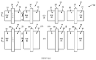
[0028] 도 1-2b는 CMOS 디바이스(10)에 초점을 두었지만, 동일한 개념들 및 문제점들이 엄격한(strictly) nMOS 디바이스 또는 엄격한 pMOS 디바이스와 같은 다른 타입들의 MOS 디바이스들에 또한 적용가능하다는 것이 인식되어야 한다. 또한, CMOS 디바이스(10)가 평면형 디바이스인 것으로 예시되지만, 동일한 기술들이 FinFET 디바이스들에 또한 이용된다. FinFET은, 실리콘 기판 또는 SOI(silicon on insulator) 기판상에 구축되는 비평면형, 이중- 또는 삼중-게이트 트랜지스터를 설명하는데 이용되는 용어이다. FinFET의 특색있는 특징은, 전도성 채널이 디바이스의 채널을 형성하는 얇은 실리콘("fin") 부근에 있다는 것이다. 핀의 길이(소스로부터 드레인의 방향으로 측정됨)는 디바이스의 유효 채널 길이를 결정한다. 1-2B focuses on the
[0029] 도 3에 예시된 대안적인 통상적 접근방식은 STI를 더미 게이트와 결합한다. 이와 관련하여, 도 3에 예시된 것처럼, CMOS 디바이스(50)는 기판(미도시)상에 형성된다. CMOS 디바이스(50)는 제 1 pMOS FET(56) 및 제 2 pMOS FET(58)뿐만 아니라 제 1 nMOS FET(52) 및 제 2 nMOS FET(54)를 포함한다. FET들(52, 54, 56, 58)은 STI(60)에 의해 서로 분리된다. 부가적으로, 더미 게이트(62)는 nMOS FET들(52, 54) 사이에 포지셔닝된다. 더미 게이트(62)는 n-금속 일함수를 갖는다. 유사하게, 더미 게이트(64)는 pMOS FET들(56, 58) 사이에 포지셔닝된다. 더미 게이트(64)는 p-금속 일함수를 갖는다. 따라서, 더미 게이트들(62, 64)의 일함수는 더미 게이트를 분리하는 FET들(52, 54 또는 56, 58)의 일함수에 대응한다. 다시, STI(60) 및 더미 게이트들(62, 64)의 사용은 (예를 들어, ~10 pA/μm 범위내의) 허용가능한 절연을 제공하지만, STI(60)의 사용은 연속 액티브 영역에 브레이크를 도입한다. 앞서 주목된 바와 같이, STI(60)는 전류 메커니즘의 원하는 모빌리티를 달성하는데 충분한 크기의 스트레스원들을 생성하는 능력에 영향을 미치며, CMOS 디바이스(50)의 성능은 더 작은 크기들에서(예를 들어, 28 나노미터 또는 이 미만의 스케일에서)는 개선되지 않는다. [0029] An alternative, conventional approach illustrated in FIG. 3 combines the STI with a dummy gate. In this regard, as illustrated in FIG. 3, the
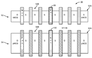
[0030] 또 다른 대안적인 통상적 접근방식이 도 4에 예시된다. 도 4는 연속 액티브 영역 방식을 통해 형성되는 CMOS 디바이스(70)를 예시한다. 특히, CMOS 디바이스(70)는 nMOS FET들(72A, 72B)(총칭하여 72) 및 pMOS FET들(74A, 74B)(총칭하여 74)를 포함한다. nMOS FET(72)는 STI(76)에 의해 pMOS FET(74)와 분리된다. 도 3의 CMOS 디바이스(50)와 달리, nMOS FET(72A)는 STI(76)에 의해 nMOS FET(72B)와 분리되지 않는다. 오히려, nMOS FET(72A) 및 nMOS FET(72B)는 연속 액티브 영역으로 형성되며 오직 더미 게이트(78)에 의해서만 분리된다. 더미 게이트(78)는 n-금속 일함수를 갖는다. 유사하게, pMOS FET(74A)는 STI(76)에 의해 pMOS FET(74B)와 분리되지 않는다. 오히려, pMOS FET(74A) 및 pMOS FET(74B)는 연속 액티브 영역으로 형성되며 오직 더미 게이트(80)에 의해서만 분리된다. 더미 게이트(80)는 p-금속 일함수를 갖는다. 이 예시적인 실시예는 연속 액티브 영역 방식으로 형성되는 장점을 갖지만, 더미 게이트들(78, 80)은 흔히 쌍을 이룬 FET들(72A, 72B) 또는 쌍을 이룬 FET들(74A, 74B) 간의 적절한 절연을 제공하지 못한다. 예를 들어, 20nm 스케일에 대한 전형적인 nMOS 구성들에서, 디바이스들은 매우 낮은 임계치 디바이스에 대해 10 nA/㎛를 가지며, 이는 STI 스타일 디바이스의 누설보다 대략 천 배 더 큰 것이다. 마찬가지로, 유사한 디바이스는 표준 임계 디바이스에 대해 대략 350 pA/㎛를 가지며, 이는 STI 스타일 디바이스의 누설보다 대략 35배 더 큰 것이다. 따라서, 하나의 nMOS FET(72A)로부터 nMOS FET(72B)으로(그리고 마찬가지로 pMOS FET(74A)로부터 pMOS FET(74B)으로) 더미 게이트(78)에 걸쳐 전류가 누설되며, 이는 CMOS 디바이스(70)의 성능을 저하시킨다. 누설 전류를 해결하기 위한 한가지 솔루션은 더미 게이트들(70, 80)에 대한 게이트 바이어스를 증가시키는 것이다. 예를 들어, nMOS FET(72)에서, 보통의 게이트 전압은 0V이지만, 전류 누설을 감소시키기 위해서는, 더미 게이트(78)에 -0.5V가 인가될 수 있다. 이러한 게이트 바이어스의 사용은 여분의 외부 전원장치를 요구하며, 이는 결국 디바이스의 풋프린트를 증가시키고 회로 복잡도를 증가시킨다. 마찬가지로, -0.5 V 게이트 바이어스로, Vgs는 Vdd(예를 들어, 0.5 V)에 도달할 수 있으며, 이는 얇은 게이트 산화물들에 대해서는 너무 높고, 게이트의 불필요한 마모(wear)를 야기할 수 있다. 유사하게, pMOS FET(74)에서, 정상적으로 절연없이, Vg = 0 V이지만 누설 전류를 감소시키기 위해서, Vg는 Vdd 또는 0.5 V로 설정될 수 있다. 다시, 이 게이트 바이어스는 여분의 외부 전원장치를 요구하며 그리고/또는 게이트 산화물 신뢰도 문제를 야기한다. 어느 경우든, 더 작은 설계 스케일들에서 CMOS 디바이스(70)가 차선이다. [0030] Another alternative conventional approach is illustrated in FIG. Figure 4 illustrates a
[0031] 상반되는 일함수를 갖는 물질로 만들어진 절연 더미 게이트로 더미 게이트(78, 80)를 교체함으로써 통상적 디바이스들의 차선의 성능(예를 들어, 속도, 누설 전류 등)에 대한 솔루션이 발견되었다. 즉, FET가 n-금속 일함수를 가지면, 더미 게이트는 p-금속 일함수를 갖는다. 대안적으로, FET들이 p-금속 일함수를 가지면, 더미 게이트는 n-금속 일함수를 갖는다. 더미 게이트 물질 선택은 여분의 외부 전원장치의 요건 없이 절연 개선을 허용하며 이에 따라 회로 내 영역이 보존된다. 마찬가지로, 이들 반도체 디바이스들을 생성하는 프로세스는 통상적으로 높은-k/금속 게이트 프로세스에서의 과도한 변화들을 요구하지 않는다. 오히려, 새로운 더미 게이트에 대해, 반대 타입 게이트 마스크(CMOS에서 사용됨)는 더미 게이트를 배치하는데 이용된다. 테스팅은, 더미 게이트의 일함수를 반대로함으로써, 연속 액티브 영역 방식을 이용하는 CMOS 디바이스를 형성하는 능력을 계속 보존하면서 허용가능한 절연 레벨들이 달성됨이 도시된다. 즉, 이 예에서, 10 pA/㎛ 범위내의 절연이 제공된다. ON 상태에서 이용가능한 전류 또한 증가되는데, 이는 해당 영역이 FET들내에서 전류 메커니즘들의 모빌리티를 증가시키는 스트레스원 엘리먼트들의 생성을 위해 보존된다는 사실로 인한 것이다. 개선된 절연과 결합된 연속 액티브 영역 방식의 사용은 추가의 최소화 및 더 큰 설계 유연성을 허용한다. Solutions have been found for lane performance (eg, speed, leakage current, etc.) of conventional devices by replacing
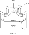
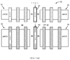
[0032] 이와 관련하여, 반대의 일함수들을 갖는 더미 게이트들을 이용하는 CMOS 디바이스(90)의 제 1 예시적 실시예가 도 5에 제공된다. 예시된 것처럼, CMOS 디바이스(90)는 연속 액티브 영역 방식을 통해 형성된다. 특히, CMOS 디바이스(90)는 nMOS FET들(92A, 92B)(총칭하여 92) 및 pMOS FET들(94A, 94B)(총칭하여 94)를 포함한다. nMOS FET(92)은 STI(96)에 의해 pMOS FET(94)와 분리된다. 도 4의 CMOS 디바이스(70)에 따라, nMOS FET(92A)은 STI(96)에 의해 nMOS FET(92B)와 분리되지 않는다. 오히려, nMOS FET(92A)와 nMOS FET(92B)는 연속 액티브 영역으로 형성되며 오직 더미 게이트(98)에 의해서만 분리된다. 더미 게이트(98)는 p-금속 일함수를 가지며 이에 따라 그가 이용되는 MOS 디바이스와 상반되는 일함수를 갖는다. 다른 식으로 말하면, 더미 게이트(98)는 반대의 일함수를 갖는다. 유사하게, pMOS FET(94A)는 STI(96)에 의해 pMOS FET(94B)와 분리되지 않는다. 오히려, pMOS FET(94A) 및 pMOS FET(94B)는 연속 액티브 영역으로 형성되며 오직 더미 게이트(100)에 의해서만 분리된다. 더미 게이트(100)는 n-금속 일함수를 가지며 이에 따라 그가 이용되는 MOS 디바이스와 상반되는 일함수를 갖는다. 다른 식으로 말하면, 더미 게이트(100)는 반대의 일함수를 갖는다. 도시되지 않았지만, 더미 게이트들(98, 100) 각각은 게이트 유전체들(28, 40)과 유사하게 게이트 유전체상에 포지셔닝된다는 것을 인식해야 한다. 예시적인 실시예에서, CMOS 디바이스(90)의 게이트 유전체는 높은 유전 상수(k)를 갖는다. 예시적인 실시예에서, k는 18 이상이며, 추가의 예시적 실시예에서, k는 대략 20-25이다. In this regard, a first exemplary embodiment of a
[0033] 계속해서 도 5를 참조로, 예시적인 실시예에서, 더미 게이트(98)는 Vss에 연결되며 더미 게이트(100)는 Vdd에 커플링된다. 주목된 것처럼, 반대의 일함수는 CMOS 디바이스(90)의 제조시 연속 액티브 영역 방식을 이용하는 제조자의 능력을 보존하면서, 허용가능한 절연 레벨들을 제공한다. 더미 게이트들(98, 100) 가까이에 소스를 배열함으로써, 절연 누설이 추가로 감소될 수 있다. [0033] Continuing to refer to FIG. 5, in the exemplary embodiment,
[0034] 도 5는 nMOS FET(92) 및 pMOS FET(94) 둘 다를 갖는 CMOS 디바이스(90)를 예시하지만, 본 개시물의 개념들이 단지 nMOS 디바이스들만을 그리고/또는 단지 pMOS 디바이스들만을 포함하는 MOS 디바이스들에 통합될 수 있다는 것이 인식되어야 한다.5 illustrates a
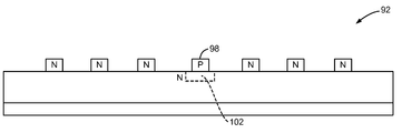
[0035] 또한, 더미 게이트들(98, 100) 아래 절연 주입 존의 부재(absence)가 주목된다. 종래 기술들, 특히 예컨대 폴리게이트 기술들은, 더미 게이트에 의해 제공되는 절연을 개선시키기 위해 더미 게이트들 밑에 이러한 절연 주입 존(즉, 특정 타입의 도핑으로 주입된 존)을 이용했을 것이다. 이러한 절연 주입 존들은 절연 크기를 증가시키며, 일반적으로, 동일 레벨의 절연을 달성하지 못한다. nMOS 디바이스(92)의 횡단면도가 도 6에 제공되며, 이는 더미 게이트(98) 밑에 절연 주입 존이 없는 존(102)을 갖는다. pMOS 디바이스(94) 또한 더미 게이트(100) 아래에 절연 주입 존을 갖지 않는다는 것이 인식되어야 한다. [0035] It is noted that the absence of the insulation injection zone under the
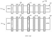
[0036] 도 5의 CMOS 디바이스(90)는 잘 이해되는 바와 같이 일반적으로 평면형 구성을 갖지만, 본 개시물의 개념들이 이로 제한되는 것은 아니며 FinFET 설계로 확장될 수 있다. 도 7a 및 도 7b는 FinFET들에서 반대의 금속 더미 게이트들에 대한 2가지 버전들을 예시한다. 특히, 도 7a는, 핀들(108)이 게이트들(110G)을 따라 수직으로 포지셔닝되는 액티브 영역(106)을 갖는 FinFET nMOS 디바이스(104)가 예시된다. FinFET nMOS 디바이스(104)는 소스들(110S) 및 드레인들(110D)을 더 포함한다. FinFET nMOS 디바이스(104)에서, 액티브 디바이스 게이트의 일 함수는 n-금속이며 대응하는 더미 게이트(112)는 p-금속 일함수를 갖는다. 더미 게이트(112) 가까이에 소스를 배열함으로써, 절연 누설이 추가로 감소될 수 있다. Although the
[0037] 도 7a의 FinFET nMOS 디바이스(104)와 대조적으로, FinFET pMOS 디바이스(114)가 도 7b에 예시된다. FinFET pMOS 디바이스(114)는 액티브 영역(116) 및 핀들(118)을 포함한다. 마찬가지로, FinFET pMOS 디바이스(114)는 드레인들(120D), 소스들(120S) 및 게이트들(120G)을 포함한다. FinFET pMOS 디바이스(114)의 액티브 영역(116)은 p-금속 일함수를 가지며 대응하는 더미 게이트(122)는 n-금속 일함수를 갖는다. 더미 게이트(122) 가까이에 소스를 배열함으로써, 절연 누설이 추가로 감소될 수 있다. [0037] In contrast to the
[0038] nMOS 디바이스(104) 및 pMOS 디바이스(114)는 원할 경우 CMOS 디바이스에 어셈블리될 수 있다. 다시, 주입 절연 존의 부재 및 높은 게이트 유전체는 크기들이 점점 더 작아짐에도 속도가 개선되게 허용한다.[0038] The
[0039] 본원에 개시된 실시예들에 따라 연속 액티브 영역들을 이용하는 CMOS 절연 방식들이 임의의 프로세서-기반 디바이스에 제공되거나 이에 통합될 수 있다. 제한 없이, 예들은 셋톱 박스, 엔터테인먼트 유닛, 네비게이션 디바이스, 통신 디바이스, 고정 로케이션 데이터 유닛, 모바일 로케이션 데이터 유닛, 모바일 폰, 셀룰러 폰, 컴퓨터, 휴대용 컴퓨터, 데스크탑 컴퓨터, PDA(personal digital assistant), 모니터, 컴퓨터 모니터, 텔레비전, 튜너, 라디오, 위성 라디오, 뮤직 플레이어, 디지털 뮤직 플레이어, 휴대용 뮤직 플레이어, 디지털 비디오 플레이어, 비디오 플레이어, DVD(digital video disc) 플레이어, 및 휴대용 디지털 비디오 플레이어를 포함한다.[0039] In accordance with the embodiments disclosed herein, CMOS isolation schemes using consecutive active regions may be provided or incorporated into any processor-based device. Without limitation, examples include a set top box, an entertainment unit, a navigation device, a communication device, a fixed location data unit, a mobile location data unit, a mobile phone, a cellular phone, a computer, a portable computer, a desktop computer, a personal digital assistant, A computer monitor, a television, a tuner, a radio, a satellite radio, a music player, a digital music player, a portable music player, a digital video player, a video player, a digital video disc player, and a portable digital video player.
[0040] 이와 관련하여, 도 8은 CMOS 디바이스(90) 또는 MOS 디바이스들(92, 94, 104, 114)과 같은 CMOS 디바이스를 이용할 수 있는 프로세서-기반 시스템(130)의 예를 예시한다. 이 예에서, 프로세서 기반 시스템(130)은 하나 또는 그 초과의 CPU(central processing unit)들(132)을 포함하며, 이 각각은 하나 또는 그 초과의 프로세서들(134)을 포함한다. CPU(들)(132)는 일시적으로 저장된 데이터에 대한 신속한 액세스를 위해 프로세서(들)(134)에 커플링되는 캐시 메모리(136)를 가질 수 있다. CPU(들)(132)는 시스템 버스(138)에 커플링되며 프로세서-기반 시스템(130)에 포함된 마스터 디바이스들 및 슬래이브 디바이스들에 상호커플링될 수 있다. 잘 알려진 것처럼, CPU(들)(132)는 시스템 버스(138)을 통해 어드레스, 제어, 및 데이터 정보를 교환함으로써 이 다른 디바이스들과 통신한다. 예를 들어, CPU(들)(132)는 메모리 제어기(140)에 버스 트랜잭션 요청들을 통신할 수 있다. 도 8에는 예시되지 않았지만, 다수의 시스템 버스들(138)이 제공될 수 있으며, 여기서 각각의 시스템 버스(138)는 서로 다른 패브릭을 구성한다. In this regard, FIG. 8 illustrates an example of a processor-based
[0041] 다른 디바이스들이 시스템 버스(138)에 연결될 수 있다. 도 8에 예시된 것처럼, 이 디바이스들은, 예들로서, 메모리 시스템(142), 하나 또는 그 초과의 입력 디바이스들(144), 하나 또는 그 초과의 출력 디바이스들(146), 하나 또는 그 초과의 네트워크 인터페이스 디바이스들(148), 및 하나 또는 그 초과의 디스플레이 제어기들(150)을 포함한다. 입력 디바이스(들)(144)는, 이로 제한되는 것은 아니나, 입력 키들, 스위치들, 보이스 프로세서들 등을 비롯한 임의의 타입의 입력 디바이스를 포함할 수 있다. 출력 디바이스(들)(146)는, 이로 제한되는 것은 아니나, 오디오, 비디오, 다른 시각적 표시자들 등을 비롯한 임의의 타입의 출력 디바이스를 포함할 수 있다. 네트워크 인터페이스 디바이스(들)(148)는, 네트워크(152)로의 그리고 네트워크(152)로부터의 데이터 교환을 허용하도록 구성된 임의의 디바이스들일 수 있다. 네트워크(152)는, 이로 제한되는 것은 아니나, 유선 또는 무선 네트워크, 사설 또는 공공 네트워크, LAN(local area network), WLAN(wide local area network) 및 인터넷을 비롯한 임의의 타입의 네트워크일 수 있다. 네트워크 인터페이스 디바이스(들)(148)는 원하는 임의의 타입의 통신 프로토콜을 지원하도록 구성될 수 있다. 메모리 시스템(142)은 하나 또는 그 초과의 메모리 유닛들(154(0-N))을 포함할 수 있다. [0041] Other devices may be coupled to the system bus 138. 8, these devices include, by way of example, a
[0042] CPU(들)(132)은 또한 하나 또는 그 초과의 디스플레이들(156)로 전송되는 정보를 제어하기 위해 시스템 버스(138)를 통해 디스플레이 제어기(들)(150)에 액세스하도록 구성될 수 있다. 디스플레이 제어기(들)(150)는, 디스플레이(들)(156)에 적합한 포맷으로 디스플레이될 정보를 프로세싱하는 하나 또는 그 초과의 비디오 프로세서들(158)을 통해 디스플레이될 정보를 디스플레이(들)(156)에 전송한다. 디스플레이(들)(156)은, 이로 제한되는 것은 아니나, CRT(cathode ray tube), LCD(liquid crystal display), 플라즈마 디스플레이 등을 비롯한 임의의 타입의 디스플레이를 포함할 수 있다. [0042] The CPU (s) 132 may also be configured to access the display controller (s) 150 via the system bus 138 to control information transmitted to one or
[0043] 당업자들은 추가로, 본원에 개시된 실시예들과 결합하여 설명되는 다양한 예시적인 논리 블록들, 모듈들, 회로들 및 알고리즘들이, 전자 하드웨어로서, 메모리에 또는 다른 컴퓨터-판독가능한 매체에 저장되며 프로세서 또는 다른 프로세싱 디바이스에 의해 실행되는 명령들로서, 또는 이 둘의 조합들에 의해 구현될 수 있음을 인식할 것이다. 본원에서 설명되는 아비터들, 마스터 디바이스들, 및 슬래이브 디바이스들은, 예들로서, 임의의 회로, 하드웨어 컴포넌트, 집적 회로(IC) 또는 IC 칩에서 이용될 수 있다. 본원에 개시된 메모리는 임의의 타입 및 크기의 메모리일 수 있으며 원하는 임의의 타입의 정보를 저장하도록 구성될 수 있다. 이 상호교환성을 명확히 하기 위해, 다양한 예시적인 컴포넌트들, 블록들, 모듈들, 회로들, 및 단계들이 일반적으로 그들의 기능적 관점에서 설명되었다. 이러한 기능이 구현되는 방식은, 전체 시스템에 부과되는 설계 제약들, 설계 선택들, 및/또는 특정 애플리케이션에 의존한다. 당업자들은 각각의 특정 애플리케이션들에 대해 가변 방식들로 설명된 기능을 구현할 수 있지만, 이러한 구현 결정들이 본 개시물의 범위 이탈을 야기하는 것으로 해석되지 않아야 한다. Those skilled in the art will further appreciate that the various illustrative logical blocks, modules, circuits and algorithms described in connection with the embodiments disclosed herein may be implemented as electronic hardware, stored in a memory or other computer- And may be implemented by instructions executed by a processor or other processing device, or by a combination of the two. The arbiters, master devices, and slave devices described herein can be used, by way of example, in any circuit, hardware component, integrated circuit (IC) or IC chip. The memory disclosed herein may be any type and size of memory and may be configured to store any type of information desired. In order to clarify this interchangeability, various illustrative components, blocks, modules, circuits, and steps have been described generally in terms of their functionality. The manner in which this functionality is implemented depends on the design constraints, design choices, and / or the particular application being imposed on the overall system. Skilled artisans may implement the described functionality in varying ways for each particular application, but such implementation decisions should not be interpreted as causing a departure from the scope of the present disclosure.
[0044] 본 개시물에 설명된 실시예들과 관련하여 설명된 다양한 예시적인 논리 블록들, 모듈들 및 회로들은 프로세서, 디지털 신호 프로세서(DSP), 주문형 집적회로(ASIC), 필드 프로그래머블 게이트 어레이(FPGA) 또는 다른 프로그래머블 논리 디바이스, 이산 게이트 또는 트랜지스터 로직, 이산 하드웨어 컴포넌트들, 또는 본원에서 설명된 기능들을 수행하도록 설계된 이들의 임의의 결합으로 구현 또는 수행될 수 있다. 프로세서는 마이크로프로세서일 수 있지만, 대안적으로, 프로세서는 임의의 종래의 프로세서, 제어기, 마이크로제어기 또는 상태 머신일 수 있다. 또한, 프로세서는 컴퓨팅 디바이스들의 결합, 예를 들어 DSP 및 마이크로프로세서의 결합, 다수의 마이크로프로세서들, DSP 코어와 결합된 하나 또는 그 초과의 마이크로프로세서들, 또는 임의의 다른 이러한 구성으로서 구현될 수 있다.[0044] The various illustrative logical blocks, modules, and circuits described in connection with the embodiments disclosed in the present disclosure may be implemented or performed with a digital signal processor (DSP), an application specific integrated circuit (ASIC), a field programmable gate array FPGA) or other programmable logic device, discrete gate or transistor logic, discrete hardware components, or any combination thereof designed to perform the functions described herein. A processor may be a microprocessor, but, in the alternative, the processor may be any conventional processor, controller, microcontroller, or state machine. A processor may also be implemented as a combination of computing devices, e.g., a combination of a DSP and a microprocessor, multiple microprocessors, one or more microprocessors in conjunction with a DSP core, or any other such configuration .
[0045] 본 개시물에 설명된 실시예들은 하드웨어로 그리고 하드웨어에 저장된 명령들로 구현될 수 있으며, 예를 들어, RAM(Random Access Memory), 플래쉬 메모리, ROM(Read Only Memory), EPROM(Electrically Programmable ROM), EEPROM(Electrically Erasable Programmable ROM), 레지스터들, 하드 디스크, 제거가능한 디스크, CD-ROM, 또는 업계에 공지된 컴퓨터 판독가능 매체의 임의의 다른 형태로서 상주할 수 있다. 예시적인 저장 매체는 프로세서와 결합되어, 프로세서가 저장 매체로부터 정보를 판독하고 저장 매체에 정보를 기록할 수 있게 된다. 대안적으로, 저장 매체는 프로세서에 통합될 수 있다. 프로세서 및 저장 매체는 ASIC에 상주할 수 있다. ASIC은 원격 스테이션에 상주할 수 있다. 대안적으로, 프로세서 및 저장 매체는 원격 스테이션, 기지국 또는 서버에서 이산 컴포넌트로서 상주할 수 있다. [0045] The embodiments described in this disclosure may be implemented in hardware and in hardware, and may include, for example, RAM (Random Access Memory), FLASH memory, ROM (Read Only Memory), EPROM Programmable ROMs, Electrically Erasable Programmable ROMs (EEPROMs), registers, hard disks, removable disks, CD-ROMs, or any other form of computer readable media known in the art. An exemplary storage medium is coupled to the processor such that the processor can read information from, and write information to, the storage medium. Alternatively, the storage medium may be integrated into the processor. The processor and the storage medium may reside in an ASIC. The ASIC may reside in a remote station. Alternatively, the processor and the storage medium may reside as discrete components in a remote station, base station, or server.
[0046] 또한, 본원의 임의의 예시적 실시예들에서 설명되는 동작 단계들은 예들 및 논의를 제공하기 위해 설명됨이 주목된다. 설명된 동작들은 예시된 시퀀스들 이외에 다수의 상이한 시퀀스들로 수행될 수 있다. 또한, 단일 동작 단계로 설명되는 동작들은 실제로 다수의 상이한 단계들로 수행될 수 있다. 부가적으로, 예시적인 실시예들에서 논의되는 하나 또는 그 초과의 동작 단계들은 결합될 수 있다. 흐름도들로 예시되는 동작 단계들은 당업자들에게 명백한 것처럼 다수의 상이한 변경들로 처리될 수 있음이 이해될 것이다. 또한 당업자들은, 정보 및 신호들이 다양한 상이한 기법들 및 기술들 중 임의의 기법 및 기술을 이용하여 표현될 수 있음을 이해할 것이다. 예를 들어, 상기 설명 전반에 걸쳐 참조될 수 있는 데이터, 명령들, 커맨드들, 정보, 신호들, 비트들, 심볼들 및 칩들은 전압들, 전류들, 전자기파들, 자기장들 또는 자기 입자들, 광 필드 또는 광 입자들, 또는 이들의 임의의 조합에 의해 표현될 수 있다.[0046] It is also noted that the operational steps described in any of the exemplary embodiments herein are described to provide examples and discussion. The described operations may be performed with a number of different sequences besides the illustrated sequences. In addition, the operations described as a single operation step may actually be performed in a number of different steps. Additionally, one or more of the operational steps discussed in the exemplary embodiments may be combined. It will be appreciated that the operating steps illustrated in the flowcharts can be handled with a number of different variations as will be apparent to those skilled in the art. Those skilled in the art will also appreciate that information and signals may be represented using any of a variety of different techniques and techniques. For example, data, instructions, commands, information, signals, bits, symbols and chips that may be referenced throughout the above description may refer to voltages, currents, electromagnetic waves, magnetic fields or magnetic particles, Light field or light particles, or any combination thereof.
[0047] 본 개시의 전술한 설명은 임의의 당업자가 본 개시를 이용하거나 또는 실시할 수 있도록 제공된다. 본 개시에 대한 다양한 변형들은 당업자들에게 용이하게 명백할 것이며, 본원에 정의된 일반적인 원리들은 본 개시의 사상 또는 범위를 벗어남이 없이 다른 변형들에 적용될 수 있다. 따라서, 본 개시는 본원에 설명된 예들 및 설계들로 제한되는 것이 아니라, 본원에 개시된 원리들 및 신규한 특징들과 일치하는 가장 넓은 범위를 따르도록 의도된다.[0047] The previous description of the disclosure is provided to enable any person skilled in the art to make or use the disclosure. Various modifications to the disclosure will be readily apparent to those skilled in the art, and the generic principles defined herein may be applied to other variations without departing from the spirit or scope of the disclosure. Accordingly, the disclosure is not intended to be limited to the examples and designs described herein, but is intended to cover the broadest scope consistent with the principles and novel features disclosed herein.
Claims (24)
제 1 n-금속 또는 p-금속 일함수를 갖는 제 1 물질;
상기 제 1 물질을 포함하는 제 1 게이트;
상기 제 1 물질을 포함하는 제 2 게이트;
상기 제 1 게이트와 상기 제 2 게이트 사이에 포지셔닝되며 상기 제 1 물질의 일함수와 상반되는 일함수를 갖는 제 2 물질을 포함하는 더미 게이트; 및
각각의 게이트 밑의 게이트 유전체
를 포함하며, 상기 게이트 유전체는 대략 18 초과의 유전 상수(k)를 포함하는, MOS 디바이스. As a metal oxide semiconductor (MOS) device,
A first material having a first n-metal or p-metal work function;
A first gate comprising the first material;
A second gate comprising the first material;
A dummy gate positioned between the first gate and the second gate and comprising a second material having a work function that is opposite to the work function of the first material; And
The gate dielectric under each gate
And wherein the gate dielectric comprises a dielectric constant (k) greater than about 18.
상기 제 1 물질은 n-금속 일함수를 갖는 물질을 포함하는, MOS 디바이스. The method according to claim 1,
Wherein the first material comprises a material having an n-metal work function.
상기 제 2 물질은 p-금속 일함수를 갖는 물질을 포함하는, MOS 디바이스. 3. The method of claim 2,
Wherein the second material comprises a material having a p-metal work function.
상기 제 1 물질은 p-금속 일함수를 갖는 물질을 포함하는, MOS 디바이스. The method according to claim 1,
Wherein the first material comprises a material having a p-metal work function.
상기 제 2 물질은 n-금속 일함수를 갖는 물질을 포함하는, MOS 디바이스. 5. The method of claim 4,
Wherein the second material comprises a material having an n-metal work function.
CMOS(complementary MOS) 디바이스를 형성하기 위해 제 2 MOS 디바이스를 더 포함하며,
상기 제 2 MOS 디바이스는,
상기 제 2 물질을 포함하는 제 3 게이트;
상기 제 2 물질을 포함하는 제 4 게이트; 및
상기 제 3 게이트와 상기 제 4 게이트 사이에 포지셔닝되며 상기 제 2 물질을 포함하는 제 2 더미 게이트
를 포함하는, MOS 디바이스. The method according to claim 1,
Further comprising a second MOS device to form a complementary MOS (CMOS) device,
Wherein the second MOS device comprises:
A third gate comprising the second material;
A fourth gate comprising the second material; And
And a second dummy gate electrode positioned between the third gate and the fourth gate,
/ RTI >
상기 제 1 MOS 디바이스와 상기 제 2 MOS 디바이스 사이의 STI(shallow trench isolation)를 더 포함하는, MOS 디바이스. The method according to claim 6,
Further comprising a shallow trench isolation (STI) between the first MOS device and the second MOS device.
상기 더미 게이트는 상기 게이트 유전체상에 포지셔닝되며 상기 더미 게이트 아래에 절연 주입 존(zone)이 없는(lack), MOS 디바이스. The method according to claim 1,
Wherein the dummy gate is positioned on the gate dielectric and lacks an insulation injection zone below the dummy gate.
상기 MOS 디바이스는 실질적으로 평면형 디바이스인, MOS 디바이스. The method according to claim 1,
Wherein the MOS device is a substantially planar device.
상기 MOS 디바이스는 FinFET(fin-based field effect transistor) 디바이스인, MOS 디바이스. The method according to claim 1,
Wherein the MOS device is a fin-based field effect transistor (" FinFET ") device.
상기 MOS 디바이스는 반도체 다이에 통합되는, MOS 디바이스. The method according to claim 1,
Wherein the MOS device is integrated into a semiconductor die.
셋톱 박스, 엔터테인먼트 유닛, 네비게이션 디바이스, 통신 디바이스, 고정 로케이션 데이터 유닛, 모바일 로케이션 데이터 유닛, 모바일 폰, 셀룰러 폰, 컴퓨터, 휴대용 컴퓨터, 데스크탑 컴퓨터, PDA(personal digital assistant), 모니터, 컴퓨터 모니터, 텔레비전, 튜너, 라디오, 위성 라디오, 뮤직 플레이어, 디지털 뮤직 플레이어, 휴대용 뮤직 플레이어, 디지털 비디오 플레이어, 비디오 플레이어, DVD(digital video disc) 플레이어, 및 휴대용 디지털 비디오 플레이어로 이루어진 그룹에서 선택되는 디바이스를 더 포함하며, 상기 디바이스는 상기 MOS 디바이스에 통합되는, MOS 디바이스. The method according to claim 1,
Such as a set top box, an entertainment unit, a navigation device, a communication device, a fixed location data unit, a mobile location data unit, a mobile phone, a cellular phone, a computer, a portable computer, a desktop computer, a personal digital assistant (PDA) Further comprising a device selected from the group consisting of a tuner, a radio, a satellite radio, a music player, a digital music player, a portable music player, a digital video player, a video player, a digital video disc player, Wherein the device is integrated into the MOS device.
제 1 n-금속 또는 p-금속 일함수를 갖기 위한 제 1 수단;
상기 제 1 수단을 포함하는 제 1 게이트 수단;
상기 제 1 수단을 포함하는 제 2 게이트 수단;
상기 제 1 게이트 수단과 상기 제 2 게이트 수단 사이에 포지셔닝되며 상기 제 1 수단의 일함수와 상반되는 일함수를 갖는 제 2 수단을 포함하는 더미 게이트 수단; 및
각각의 게이트 수단 밑의 게이트 유전체
를 포함하며, 상기 게이트 유전체는 대략 18 초과의 유전 상수(k)를 포함하는, MOS 디바이스.As a metal oxide semiconductor (MOS) device,
First means for having a first n-metal or p-metal work function;
First gate means comprising said first means;
Second gate means comprising said first means;
Dummy gate means positioned between said first gate means and said second gate means and comprising second means having a work function opposite to the work function of said first means; And
The gate dielectric under each gate means
And wherein the gate dielectric comprises a dielectric constant (k) greater than about 18.
제 1 n-금속 또는 p-금속 일함수를 갖는 제 1 물질을 제공하는 단계;
액티브 영역 상에 게이트 유전체를 형성하는 단계 ―상기 게이트 유전체는 대략 18 초과의 유전 상수(k)를 포함함―;
상기 게이트 유전체 상에 상기 제 1 물질을 포함하는 제 1 게이트를 형성하는 단계;
상기 게이트 유전체 상에 상기 제 1 물질을 포함하는 제 2 게이트를 형성하는 단계;
상기 게이트 유전체 상에 더미 게이트를 형성하는 단계 ―상기 더미 게이트는 상기 제 1 물질의 일함수와 상반되는 일함수를 갖는 제 2 물질을 포함함―; 및
상기 제 1 물질의 일함수와 상반되는 일함수를 갖는 제 2 물질을 포함하는 상기 더미 게이트를 상기 제 1 게이트와 상기 제 2 게이트 사이에 포지셔닝하는 단계
를 포함하는, MOS 디바이스를 형성하는 방법.1. A method of forming a metal oxide semiconductor (MOS) device,
Providing a first material having a first n-metal or p-metal work function;
Forming a gate dielectric on the active region, wherein the gate dielectric comprises a dielectric constant (k) greater than about 18;
Forming a first gate comprising the first material on the gate dielectric;
Forming a second gate comprising the first material on the gate dielectric;
Forming a dummy gate on the gate dielectric, the dummy gate comprising a second material having a work function that is opposite to the work function of the first material; And
Positioning the dummy gate between the first gate and the second gate comprising a second material having a work function opposite to the work function of the first material;
/ RTI > A method of forming a MOS device,
상기 더미 게이트를 형성하는 단계는 절연 주입 존이 없는 로케이션에 상기 더미 게이트를 형성하는 단계를 포함하는, MOS 디바이스를 형성하는 방법.15. The method of claim 14,
Wherein forming the dummy gate includes forming the dummy gate in a location free of an insulative implantation zone.
상기 게이트 유전체를 형성하는 단계는 대략 20-25의 유전 상수를 갖는 상기 게이트 유전체를 형성하는 단계를 포함하는, MOS 디바이스를 형성하는 방법.15. The method of claim 14,
Wherein forming the gate dielectric comprises forming the gate dielectric having a dielectric constant of approximately 20-25.
상기 제 1 물질은 n-금속 일함수를 갖는 물질을 포함하며, 상기 제 2 물질은 p-금속 일함수를 갖는 물질을 포함하는, MOS 디바이스를 형성하는 방법.15. The method of claim 14,
Wherein the first material comprises a material having an n-metal work function and the second material comprises a material having a p-metal work function.
상기 제 2 게이트를 접지에 연결하는 단계를 더 포함하는, MOS 디바이스를 형성하는 방법.18. The method of claim 17,
And connecting the second gate to ground. ≪ Desc / Clms Page number 20 >
상기 제 2 게이트 가까이에 소스를 형성하는 단계를 더 포함하는, MOS 디바이스를 형성하는 방법.18. The method of claim 17,
And forming a source near said second gate. ≪ Desc / Clms Page number 21 >
상기 제 1 물질은 p-금속 일함수를 갖는 물질을 포함하며, 상기 제 2 물질은 n-금속 일함수를 갖는 물질을 포함하는, MOS 디바이스를 형성하는 방법.15. The method of claim 14,
Wherein the first material comprises a material having a p-metal work function and the second material comprises a material having an n-metal work function.
전압원에 상기 제 2 게이트를 연결하는 단계를 더 포함하는, MOS 디바이스를 형성하는 방법.21. The method of claim 20,
And connecting the second gate to a voltage source.
상기 제 2 게이트 가까이에 소스를 형성하는 단계를 더 포함하는, MOS 디바이스를 형성하는 방법.21. The method of claim 20,
And forming a source near said second gate. ≪ Desc / Clms Page number 21 >
CMOS 디바이스를 형성하기 위해 상기 제 1 MOS 디바이스와 함께 상기 제 2 MOS 디바이스를 형성하는 단계를 더 포함하는, MOS 디바이스를 형성하는 방법.15. The method of claim 14,
Further comprising forming the second MOS device with the first MOS device to form a CMOS device.
상기 제 2 MOS 디바이스를 형성하는 단계는, 상기 제 2 MOS 디바이스내에 더미 게이트를 형성하는 단계를 포함하는, MOS 디바이스를 형성하는 방법.
24. The method of claim 23,
Wherein forming the second MOS device comprises forming a dummy gate in the second MOS device.
Applications Claiming Priority (3)
| Application Number | Priority Date | Filing Date | Title |
|---|---|---|---|
| US13/799,955 | 2013-03-13 | ||
| US13/799,955 US9997617B2 (en) | 2013-03-13 | 2013-03-13 | Metal oxide semiconductor (MOS) isolation schemes with continuous active areas separated by dummy gates and related methods |
| PCT/US2014/022263 WO2014159160A1 (en) | 2013-03-13 | 2014-03-10 | Metal oxide semiconductor (mos) isolation schemes with continuous active areas separated by dummy gates and related methods |
Publications (1)
| Publication Number | Publication Date |
|---|---|
| KR20150131090A true KR20150131090A (en) | 2015-11-24 |
Family
ID=50487119
Family Applications (1)
| Application Number | Title | Priority Date | Filing Date |
|---|---|---|---|
| KR1020157027562A KR20150131090A (en) | 2013-03-13 | 2014-03-10 | Metal oxide semiconductor (mos) isolation schemes with continuous active areas separated by dummy gates and related methods |
Country Status (6)
| Country | Link |
|---|---|
| US (2) | US9997617B2 (en) |
| EP (1) | EP2973682A1 (en) |
| JP (2) | JP2016516301A (en) |
| KR (1) | KR20150131090A (en) |
| CN (1) | CN105009275A (en) |
| WO (1) | WO2014159160A1 (en) |
Families Citing this family (20)
| Publication number | Priority date | Publication date | Assignee | Title |
|---|---|---|---|---|
| WO2015025441A1 (en) | 2013-08-23 | 2015-02-26 | パナソニック株式会社 | Semiconductor integrated circuit device |
| US9318476B2 (en) * | 2014-03-03 | 2016-04-19 | Qualcomm Incorporated | High performance standard cell with continuous oxide definition and characterized leakage current |
| US10468528B2 (en) | 2014-04-16 | 2019-11-05 | Taiwan Semiconductor Manufacturing Company, Ltd. | FinFET device with high-k metal gate stack |
| US9209185B2 (en) | 2014-04-16 | 2015-12-08 | Taiwan Semiconductor Manufacturing Company, Ltd. | Method and structure for FinFET device |
| US9721955B2 (en) | 2014-04-25 | 2017-08-01 | Taiwan Semiconductor Manufacturing Company, Ltd. | Structure and method for SRAM FinFET device having an oxide feature |
| US9178067B1 (en) | 2014-04-25 | 2015-11-03 | Taiwan Semiconductor Manufacturing Company, Ltd. | Structure and method for FinFET device |
| US9224736B1 (en) | 2014-06-27 | 2015-12-29 | Taiwan Semicondcutor Manufacturing Company, Ltd. | Structure and method for SRAM FinFET device |
| KR102202754B1 (en) * | 2014-08-14 | 2021-01-15 | 삼성전자주식회사 | Semiconductor device |
| US10361195B2 (en) * | 2014-09-04 | 2019-07-23 | Samsung Electronics Co., Ltd. | Semiconductor device with an isolation gate and method of forming |
| US9502414B2 (en) * | 2015-02-26 | 2016-11-22 | Qualcomm Incorporated | Adjacent device isolation |
| US9899266B2 (en) | 2016-05-02 | 2018-02-20 | Taiwan Semiconductor Manufacturing Company, Ltd. | FinFET structures and methods of forming the same |
| CN109417033B (en) * | 2016-06-28 | 2022-03-18 | 株式会社索思未来 | Semiconductor device and semiconductor integrated circuit |
| US9997360B2 (en) * | 2016-09-21 | 2018-06-12 | Qualcomm Incorporated | Method for mitigating layout effect in FINFET |
| KR102240021B1 (en) | 2017-03-03 | 2021-04-14 | 삼성전자주식회사 | Semiconductor device including a resistor |
| KR102449898B1 (en) | 2018-04-10 | 2022-09-30 | 삼성전자주식회사 | Integrated circuit device |
| US10679994B1 (en) * | 2018-11-28 | 2020-06-09 | Qualcomm Incorporated | Circuits employing asymmetric diffusion breaks in different type semiconductor diffusion regions, and related fabrication methods |
| US11145550B2 (en) | 2020-03-05 | 2021-10-12 | International Business Machines Corporation | Dummy fin template to form a self-aligned metal contact for output of vertical transport field effect transistor |
| US20220231134A1 (en) * | 2021-01-18 | 2022-07-21 | Samsung Electronics Co., Ltd. | Selective single diffusion/electrical barrier |
| US11646361B2 (en) | 2021-03-04 | 2023-05-09 | Globalfoundries U.S. Inc. | Electrical isolation structure using reverse dopant implantation from source/drain region in semiconductor fin |
| US20220416026A1 (en) * | 2021-06-29 | 2022-12-29 | Taiwan Semiconductor Manufacturing Company, Ltd. | Semiconductor device and method of manufacturing the same |
Family Cites Families (22)
| Publication number | Priority date | Publication date | Assignee | Title |
|---|---|---|---|---|
| US5122474A (en) | 1988-06-23 | 1992-06-16 | Dallas Semiconductor Corporation | Method of fabricating a CMOS IC with reduced susceptibility to PMOS punchthrough |
| US5268312A (en) | 1992-10-22 | 1993-12-07 | Motorola, Inc. | Method of forming isolated wells in the fabrication of BiCMOS devices |
| JPH08153861A (en) * | 1994-11-29 | 1996-06-11 | Hitachi Ltd | Semiconductor device and manufacture thereof |
| JP2907070B2 (en) | 1995-08-11 | 1999-06-21 | 日本電気株式会社 | Method for manufacturing semiconductor device |
| FR2785089B1 (en) | 1998-10-23 | 2002-03-01 | St Microelectronics Sa | CONSTRUCTION OF INSULATION WALL |
| JP2001345430A (en) | 2000-05-31 | 2001-12-14 | Hitachi Ltd | Semiconductor integrated circuit device and manufacturing method thereof |
| US6620713B2 (en) * | 2002-01-02 | 2003-09-16 | Intel Corporation | Interfacial layer for gate electrode and high-k dielectric layer and methods of fabrication |
| US6756619B2 (en) | 2002-08-26 | 2004-06-29 | Micron Technology, Inc. | Semiconductor constructions |
| JP4209206B2 (en) | 2003-01-14 | 2009-01-14 | 富士通マイクロエレクトロニクス株式会社 | Manufacturing method of semiconductor device |
| JP2005064317A (en) | 2003-08-18 | 2005-03-10 | Semiconductor Leading Edge Technologies Inc | Semiconductor device |
| JP2007311491A (en) | 2006-05-17 | 2007-11-29 | Toshiba Corp | Semiconductor integrated circuit |
| JP2008103488A (en) * | 2006-10-18 | 2008-05-01 | Seiko Epson Corp | Manufacturing method for semiconductor integrated circuit device, and semiconductor device |
| US20100127333A1 (en) | 2008-11-21 | 2010-05-27 | Taiwan Semiconductor Manufacturing Company, Ltd. | novel layout architecture for performance enhancement |
| US8324668B2 (en) * | 2009-12-17 | 2012-12-04 | Taiwan Semiconductor Manufacturing Company, Ltd. | Dummy structure for isolating devices in integrated circuits |
| US8390331B2 (en) | 2009-12-29 | 2013-03-05 | Nxp B.V. | Flexible CMOS library architecture for leakage power and variability reduction |
| US8598656B2 (en) | 2010-03-08 | 2013-12-03 | Taiwan Semiconductor Manufacturing Company, Ltd. | Method and apparatus of forming ESD protection device |
| US8212295B2 (en) | 2010-06-30 | 2012-07-03 | Taiwan Semiconductor Manufacturing Company, Ltd. | ROM cell circuit for FinFET devices |
| US9324866B2 (en) * | 2012-01-23 | 2016-04-26 | Taiwan Semiconductor Manufacturing Company, Ltd. | Structure and method for transistor with line end extension |
| US8455180B2 (en) * | 2010-10-29 | 2013-06-04 | Texas Instruments Incorporated | Gate CD control using local design on both sides of neighboring dummy gate level features |
| US8378419B2 (en) * | 2010-11-22 | 2013-02-19 | International Business Machines Corporation | Isolation FET for integrated circuit |
| US8547155B2 (en) * | 2011-08-22 | 2013-10-01 | Cisco Technology, Inc. | Soft error robust low power latch device layout techniques |
| US9337190B2 (en) * | 2013-03-12 | 2016-05-10 | Taiwan Semiconductor Manufacturing Company, Ltd. | Semiconductor device including dummy isolation gate structure and method of fabricating thereof |
-
2013
- 2013-03-13 US US13/799,955 patent/US9997617B2/en active Active
-
2014
- 2014-03-10 WO PCT/US2014/022263 patent/WO2014159160A1/en active Application Filing
- 2014-03-10 KR KR1020157027562A patent/KR20150131090A/en active IP Right Grant
- 2014-03-10 CN CN201480013153.8A patent/CN105009275A/en active Pending
- 2014-03-10 EP EP14717545.9A patent/EP2973682A1/en not_active Ceased
- 2014-03-10 JP JP2016500931A patent/JP2016516301A/en active Pending
-
2018
- 2018-04-24 JP JP2018082923A patent/JP2018113485A/en active Pending
- 2018-04-25 US US15/962,023 patent/US20180240890A1/en not_active Abandoned
Also Published As
| Publication number | Publication date |
|---|---|
| US20140264610A1 (en) | 2014-09-18 |
| EP2973682A1 (en) | 2016-01-20 |
| US9997617B2 (en) | 2018-06-12 |
| JP2018113485A (en) | 2018-07-19 |
| WO2014159160A1 (en) | 2014-10-02 |
| JP2016516301A (en) | 2016-06-02 |
| US20180240890A1 (en) | 2018-08-23 |
| CN105009275A (en) | 2015-10-28 |
Similar Documents
| Publication | Publication Date | Title |
|---|---|---|
| US20180240890A1 (en) | Metal oxide semiconductor (mos) isolation schemes with continuous active areas separated by dummy gates and related methods | |
| US10020231B2 (en) | Semiconductor device and method for fabricating the same | |
| US9299811B2 (en) | Methods of fabricating semiconductor devices | |
| US8592290B1 (en) | Cut-very-last dual-EPI flow | |
| US20160336324A1 (en) | Tunnel field effect transistor and method of making the same | |
| US20140220752A1 (en) | Semiconductor device and method of fabricating the same | |
| KR20150058597A (en) | Semiconductor device and method for fabricating the same | |
| KR20140122638A (en) | Semiconductor package and method for fabricating the same | |
| CN110036487A (en) | Asymmetric grid-control fin formula field effect transistor (FET) (finFET) diode | |
| EP3378095B1 (en) | Semiconductor devices with wider field gates for reduced gate resistance | |
| KR102550579B1 (en) | FIN Field Effect Transistors (FETs) Using Dielectric Material Layers to Apply Stress to Channel Regions (FINFETs) | |
| CN104916545A (en) | Semiconductor device manufacturing method | |
| US11424335B2 (en) | Group III-V semiconductor devices having dual workfunction gate electrodes | |
| US10600774B2 (en) | Systems and methods for fabrication of gated diodes with selective epitaxial growth | |
| US20190296126A1 (en) | Systems and methods for dummy gate tie-offs in a self-aligned gate contact (sagc) cell | |
| AU2017325703B2 (en) | Semiconductor devices employing field effect transistors (FETs) with multiple channel structures without shallow trench isolation (STI) void-induced electrical shorts | |
| US11164747B2 (en) | Group III-V semiconductor devices having asymmetric source and drain structures |
Legal Events
| Date | Code | Title | Description |
|---|---|---|---|
| A201 | Request for examination | ||
| E902 | Notification of reason for refusal | ||
| E701 | Decision to grant or registration of patent right |