KR20150080098A - Semiconductor apparatus - Google Patents
Semiconductor apparatus Download PDFInfo
- Publication number
- KR20150080098A KR20150080098A KR1020130167019A KR20130167019A KR20150080098A KR 20150080098 A KR20150080098 A KR 20150080098A KR 1020130167019 A KR1020130167019 A KR 1020130167019A KR 20130167019 A KR20130167019 A KR 20130167019A KR 20150080098 A KR20150080098 A KR 20150080098A
- Authority
- KR
- South Korea
- Prior art keywords
- inverters
- inverter
- drain
- wiring
- terminal
- Prior art date
- Legal status (The legal status is an assumption and is not a legal conclusion. Google has not performed a legal analysis and makes no representation as to the accuracy of the status listed.)
- Withdrawn
Links
- 239000004065 semiconductor Substances 0.000 title claims abstract description 8
- 230000000630 rising effect Effects 0.000 claims description 13
- 238000000034 method Methods 0.000 claims description 7
- 239000000470 constituent Substances 0.000 description 2
- 238000010586 diagram Methods 0.000 description 2
- 238000012986 modification Methods 0.000 description 1
- 230000004048 modification Effects 0.000 description 1
Images

Classifications
-
- H—ELECTRICITY
- H03—ELECTRONIC CIRCUITRY
- H03K—PULSE TECHNIQUE
- H03K19/00—Logic circuits, i.e. having at least two inputs acting on one output; Inverting circuits
- H03K19/0175—Coupling arrangements; Interface arrangements
- H03K19/0185—Coupling arrangements; Interface arrangements using field effect transistors only
- H03K19/018507—Interface arrangements
- H03K19/018521—Interface arrangements of complementary type, e.g. CMOS
-
- G—PHYSICS
- G11—INFORMATION STORAGE
- G11C—STATIC STORES
- G11C5/00—Details of stores covered by group G11C11/00
- G11C5/06—Arrangements for interconnecting storage elements electrically, e.g. by wiring
Landscapes
- Engineering & Computer Science (AREA)
- Computer Hardware Design (AREA)
- Physics & Mathematics (AREA)
- Computing Systems (AREA)
- General Engineering & Computer Science (AREA)
- Mathematical Physics (AREA)
- Semiconductor Integrated Circuits (AREA)
- Metal-Oxide And Bipolar Metal-Oxide Semiconductor Integrated Circuits (AREA)
Abstract
본 기술에 따른 반도체 장치는 복수 개의 인버터가 직렬 연결되는 인버터 체인을 포함하고, 상기 복수 개의 인버터들 중 적어도 하나는 복수 개의 출력노드를 포함할 수 있다.A semiconductor device according to the present invention includes an inverter chain in which a plurality of inverters are serially connected, and at least one of the plurality of inverters may include a plurality of output nodes.
Description
본 발명은 반도체 장치에 관한 것으로, 더욱 상세하게는 라이징 타임과 폴링 타임을 개선할 수 있는 인버터 체인을 포함하는 반도체 장치에 관한 것이다.The present invention relates to a semiconductor device, and more particularly, to a semiconductor device including an inverter chain capable of improving a rising time and a polling time.
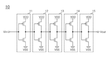
도 1 및 도 2를 참조하면, 종래의 인버터 체인(10)은 복수 개의 인버터(11,12,13,14,15)로 구성될 수 있다.Referring to FIGS. 1 and 2, the
상기의 인버터 체인(10)의 각 인버터의 출력단은 도시된 바와 같이 다음으로 연결되는 인버터의 입력단과 연결된다. 예를 들면, 제1인버터(11)의 출력단은 제2인버터(12)의 입력단과 연결된다. 이때, 제1,2인버터(11,12)의 연결은 제1인버터(11)의 출력단의 중간에서 제2인버터(12)의 입력단과 단 한번만 연결된다. The output terminals of the inverters of the
부연하면, 각 인버터(11,12,13,14,15)의 출력단은 인터버를 구성하는 PMOS 트랜지스터의 드레인단자(PD)과 NMOS 트랜지스터의 드레인단자(ND)을 연결하는 배선(20)의 중간의 위치에 배치된다. 그리고 각 인버터(11,12,13,14,15)의 입력단은 PMOS 트랜지스터의 게이트단자(PG)와 NMOS 트랜지스터의 게이트단자(NG)를 연결하는 배선(30)의 중간의 위치에 배치된다.The output terminals of the
이로 인해 종래에는 상술한 바와 같이 어느 하나의 인버터의 출력단 중간에서 다음 인버터의 입력단과 연결되는 패스(Path)를 가짐에 따라, 각 인버터의 라이징(Rising) 또는 폴링(Falling) 동작 시 라이징 타임(Rising time) 및 폴링 타임(Falling time)에서 손해를 보게 된다.As a result, as described above, since a path is connected to the input terminal of the next inverter from the middle of the output terminal of one inverter, a rising time (Rising) of each inverter in the rising or falling operation time and the falling time.
본 발명의 실시예는 복수 개의 인버터가 직렬 연결되는 인버터 체인에서 라이징 타임 및 폴링 타임을 개선할 수 있는 반도체 장치를 제공한다.An embodiment of the present invention provides a semiconductor device capable of improving a rising time and a polling time in an inverter chain in which a plurality of inverters are serially connected.
본 발명의 실시예에 따른 반도체 장치는 복수 개의 인버터가 직렬 연결되는 인버터 체인을 포함하고, 상기 복수 개의 인버터들 중 적어도 하나는 복수 개의 출력노드를 포함할 수 있다.A semiconductor device according to an embodiment of the present invention includes an inverter chain in which a plurality of inverters are serially connected, and at least one of the plurality of inverters may include a plurality of output nodes.
본 기술에 의하면, 전류 패스 거리가 짧은 라이징 패스와 폴링 패스를 가짐에 따라 인버터 체인의 라이징 타임 및 폴링 타임의 효율을 높일 수 있다.According to this technology, since the current path length is short and the rising path and the polling path are short, the efficiency of the rising time and polling time of the inverter chain can be increased.
도 1은 종래의 인버터 체인의 회로도이다.
도 2는 도 1에 도시된 인버터 체인의 레이아웃도이다.
도 3은 본 발명의 실시예에 따른 인버터 체인의 회로도이다.
도 4는 도 3에 도시된 인버터 체인의 레이아웃도이다.1 is a circuit diagram of a conventional inverter chain.
2 is a layout view of the inverter chain shown in Fig.
3 is a circuit diagram of an inverter chain according to an embodiment of the present invention.
4 is a layout view of the inverter chain shown in Fig.
이하, 첨부한 도면을 참조하여 본 발명의 바람직한 실시예를 설명하기로 한다. 그러나, 본 발명은 여기서 설명되는 실시예들에 한정되지 않고 다른 형태로 구체화될 수도 있다. 그리고 본 발명의 요지와 무관한 공지의 구성은 생략될 수 있다. 각 도면의 구성요소들에 참조 번호를 부가함에 있어서, 동일한 구성 요소들에 한해서는 비록 다른 도면상에 표시되더라도 가능한 한 동일한 번호를 가지도록 하고 있음에 유의하여야 한다.Hereinafter, preferred embodiments of the present invention will be described with reference to the accompanying drawings. However, the present invention is not limited to the embodiments described herein but may be embodied in other forms. And a known configuration irrelevant to the gist of the present invention may be omitted. It should be noted that, in the case of adding the reference numerals to the constituent elements of the drawings, the same constituent elements have the same number as much as possible even if they are displayed on different drawings.
도 3 및 도 4를 참조하면, 인버터 체인(100)은 상호 직렬 연결되는 복수 개의 인버터로 구성되는데, 본 발명의 실시예에서는 도시된 바와 같이 다섯 개의 인버터(110,120,130,140,150)로 구성될 수 있다. 예를 들면, 인버터 체인(100)은 복수 개의 인버터가 직렬 연결되는 오실레이터일 수 있다.Referring to FIGS. 3 and 4, the
구체적으로, 제1인버터(110)는 입력단(Vin)과 연결되는 게이트단자(PG1)와, 전원 전압단(VDD)에 연결되는 소스단자(PS1) 및 제1출력노드(N1)에 연결되는 드레인단자(PD1)를 갖는 제1PMOS 트랜지스터(PM1)와, 입력단(Vin)과 연결된 게이트단자(NG1)와, 접지 전압단(VSS)에 연결되는 소스단자(NS1) 및 제2출력노드(N2)와 연결되는 드레인단자(ND1)를 갖는 제1NMOS 트랜지스터(NM1)를 포함한다.Specifically, the
제2인버터(120)는 제1입력노드(N1')와 연결되는 게이트단자(PG2)와, 전원 전압단(VDD)과 연결되는 소스단자(PS2) 및 제3출력노드(N3)에 연결되는 드레인단자(PD2)를 갖는 제2PMOS 트랜지스터(PM2)와, 제2입력노드(N2')와 연결되는 게이트단자(NG2)와, 접지 전압단(VSS)에 연결되는 소스단자(NS2) 및 제4출력노드(N4)와 연결되는 드레인단자(ND2)를 갖는 제2NMOS 트랜지스터(NM2)를 포함한다.The
제3인버터(130)는 제3입력노드(N3')와 연결되는 게이트단자(PG3)와, 전원 전압(VDD)단과 연결되는 소스단자(PS3) 및 제5출력노드(N5)에 연결되는 드레인단자(PD3)를 갖는 제3PMOS 트랜지스터(PM3)와, 제4입력노드(N4')와 연결되는 게이트단자(NG3)와, 접지 전압단(VSS)에 연결되는 소스(NS3) 및 제6출력노드(N6)와 연결되는 드레인단자(ND3)를 갖는 제3NMOS 트랜지스터(NM3)를 포함한다.The
제4인버터(140)는 제5입력노드(N5')와 연결되는 게이트단자(PG4)와, 전원 전압(VDD)단에 연결되는 소스단자(PS4) 및 제7출력노드(N7)에 연결되는 드레인단자(PD4)을 갖는 제4PMOS 트랜지스터(PM4)와, 제6입력노드(N6')와 연결되는 게이트단자(NG4)와, 접지 전압단(VSS)에 연결되는 소스(NS4) 및 제8출력노드(N8)에 연결되는 드레인단자(ND4)를 갖는 제4NMOS 트랜지스터(NM4)를 포함한다.The
제5인버터(150)는 제7입력노드(N7')와 연결되는 게이트단자(PG5)와, 전원 전압단(VDD)에 연결되는 소스단자(PS5) 및 출력단(Vout)에 연결되는 드레인단자(PD5)을 갖는 제5PMOS 트랜지스터(PM5)와, 제8입력노드(N8')와 연결되는 게이트단자(NG5)와, 접지 전압단(VSS)에 연결되는 소스(NS5) 및 출력단(Vout)에 연결되는 드레인단자(ND5)를 갖는 제5NMOS 트랜지스터(NM5)를 포함한다.The
즉, 본 발명의 실시예에서 인버터 체인(100)을 구성하는 인버터들 중 일부(예를 들면, 제1,2,3,4인버터)는 상술한 바와 같이 복수 개의 출력노드(N1,N2,N3,N4,N5,N6,N7,N8,N9)를 갖는다. In other words, in the embodiment of the present invention, some of the inverters constituting the inverter chain 100 (for example, the first, second, third and fourth inverters) are connected to the output nodes N1, N2 and N3 , N4, N5, N6, N7, N8, N9).
부연 설명하면, 제1,2,3,4인버터(110,120,130,140)는 PMOS 트랜지스터(PM1,PM2,PM3,PM4)와, NMOS 트랜지스터(NM1,NM2,NM3,NM4)를 포함한다. 그리고 제1,2,3,4인버터(110,120,130,140)의 복수 개의 출력노드(N1,N2,N3,N4,N5,N6,N7,N8)는 각 트랜지스터의 드레인단자를 연결하는 배선(이하, 드레인 배선으로 지칭,111,121,131,141,151)과 후속 연결되는 인버터(예를 들면, 제2,3,4,5인버터)의 각 트랜지스터의 게이트단자를 연결하는 배선(이하, 게이트 배선으로 지칭,113,123,133,143,153)을 연결하는 복수 개의 연결배선을 통해 형성될 수 있다.In other words, the first, second, third and
이때, 상기의 복수 개의 연결배선은 각 인버터(110,120,130,140,150)의 드레인 배선(111,121,131,141,151) 상에서 PMOS 트랜지스터의 드레인단자(PD1,PD2,PD3,PD4,PD5)와 인접한 위치에 연결되는 제1연결배선(161a,162a,163a,164a)과, 각 인버터(110,120,130,140,150)의 드레인 배선(111,121,131,141,151) 상에서 NMOS 트랜지스터의 드레인단자(ND1,ND2,ND3,ND4,ND5)와 인접한 위치에 연결되는 제2연결배선(161b,162b,163b,164b)을 포함할 수 있다.The plurality of connection wirings may include
상기의 설명에서 PMOS 트랜지스터의 드레인단자(PD1,PD2,PD3,PD4,PD5)와 인접한 위치란 드레인 배선((111,121,131,141,151) 상에서 드레인 배선(111,121,131,141,151)의 중간 보다 PMOS 트랜지스터의 드레인단자(PD1,PD2,PD3,PD4,PD5)에 가까운 위치를 말한다. In the above description, the position adjacent to the drain terminals PD1, PD2, PD3, PD4, and PD5 of the PMOS transistor is larger than the middle of the
그리고 NMOS 트랜지스터의 드레인단자(ND1,ND2,ND3,ND4,ND5)와 인접한 위치란 드레인 배선(111,121,131,141,151) 상에서 드레인 배선(111,121,131,141,151)의 중간 보다 NMOS 트랜지스터의 드레인단자(ND1,ND2,ND3,ND4,ND5)에 가까운 위치를 말한다.The drain terminals ND1, ND2, ND3, ND4 and ND5 of the NMOS transistors are connected to the drain terminals of the NMOS transistors adjacent to the drain terminals ND1, ND2, ND3, ND4 and ND5 of the NMOS transistors on the
또한, 본 발명의 실시예에서 상술한 바와 같이 인버터들 중 일부(제1,2,3,4인버터(110,120,130,140))에는 복수 개의 출력노드(N1,N2,N3,N4,N5,N6,N7,N8)가 형성되고, 상기의 일부의 인버터 다음으로 연결되는 인버터(제2,3,4,5인버터(120,130,140,150))에는 상기의 복수 개의 출력노드(N1,N2,N3,N4,N5,N6,N7,N8)와 각각 연결되는 복수 개의 입력노드(N1',N2',N3',N4',N5',N6',N7',N8')가 형성될 수 있다.In the embodiment of the present invention, a plurality of output nodes N1, N2, N3, N4, N5, N6, N7, and N6 are provided in some of the inverters (first, second, third, and
또한, 본 발명의 실시예에서는 상술한 바와 같이 연결배선을 제1,2연결배선을 예로 들어 설명하였으나, 더 많은 숫자의 연결배선을 포함할 수도 있다.
Also, in the embodiment of the present invention, as described above, the first and second connection wirings are described as an example of the connection wirings, but may include a larger number of connection wirings.
한편, 본 발명의 실시예에 따른 인버터 체인 회로의 동작을 살펴보면 다음과 같다.The operation of the inverter chain circuit according to the embodiment of the present invention will be described below.
제1인버터(110)의 입력단으로 로우 레벨의 전위가 입력되면, 제1인버터(110)에서는 제1PMOS 트랜지스터(PM1)가 턴온되고, 제2인버터(120)에서는 제2NMOS 트랜지스터(NM2)가 턴온되고, 제3인버터(130)에서는 제3PMOS 트랜지스터(PM3)가 턴온되고, 제4인버터(140)에서는 제4NMOS트랜지스터(NM4)가 턴온되고, 제5인버터(150)에서는 제5PMOS 트랜지스터(PM5)가 턴온되어 하이 레벨의 전위가 출력될 수 있다.When the low level potential is input to the input terminal of the
상기의 과정에서 제1,2인버터(110,120)에서는 전원 전압(VDD)의 전류가 제1인버터(110)의 드레인 배선(111)에서 제1연결배선(161a)을 통해 제2인버터(120)의 게이트 배선(123)으로 흐르는 제1라이징 패스(Rising path)가 형성된다.In the first and
그리고 제2,3인버터(120,130)에서는 접지 전압(VSS)의 전류가 제2인버터(120)의 드레인 배선(121)에서 제2연결배선(162b)을 통해 제3인버터(130)의 게이트 배선(133)으로 흐르는 제1폴링 패스(Falling path)가 형성된다.In the second and
제3,4인버터(130,140)에서는 전원 전압(VDD)의 전류가 제3인버터(130)의 드레인 배선(131)에서 제1연결배선(163a)을 통해 제4인버터(140)의 게이트 배선(143)으로 흐르는 제2라이징 패스가 형성된다.In the third and
제4,5인버터(140,150)에서는 접지 전압(VSS)의 전류가 제4인버터(140)의 드레인 배선(141)에서 제2연결배선(164b)을 통해 제5인버터(150)의 게이트 배선(153)으로 흐르는 제2폴링 패스가 형성된다.In the fourth and
상기의 과정에서 각 제1연결배선(161a,162a,163a,164a)은 드레인 배선(111,121,131,141,151) 상에서 PMOS 트랜지스터의 드레인단자(PM1,PM2,PM3,PM4)와 인접한 위치에 연결됨에 따라, 라이징 패스의 거리가 짧아지게 된다. 이로 인해 본 발명의 실시예에서는 인버터 체인의 라이징 타임 역시 짧아지게 된다.In the above process, the
또, 각 제2연결배선(161b,162b,163b,164b)은 드레인 배선(111,121,131,141,151) 상에서 NMOS 트랜지스터의 드레인단자(NM1,NM2,NM3,NM4)와 인접한 위치에 연결됨에 따라, 폴링 패스의 거리가 짧아지게 된다. 이로 인해 본 발명의 실시예에서는 인버터의 폴링 타임 역시 짧아지게 된다.Since the
따라서 본 발명의 실시예에서는 라이징 패스와 폴링 패스의 개선을 통해 인버터의 라이징 타임 및 폴링 타임의 효율을 높일 수 있게 된다.Therefore, in the embodiment of the present invention, it is possible to improve the rising time of the inverter and the efficiency of the polling time by improving the rising path and the polling path.
본 발명이 속하는 기술분야의 당업자는 본 발명이 그 기술적 사상이나 필수적 특징으로 변경하지 않고서 다른 구체적인 형태로 실시될 수 있으므로, 이상에서 기술한 실시예들은 모든 면에서 예시적인 것이며 한정적인 것이 아닌 것으로서 이해해야만 한다. 본 발명의 범위는 상기의 상세한 설명보다는 후술하는 특허청구범위에 의하여 나타내어지며, 특허청구범위의 의미 및 범위 그리고 그 등가개념으로부터 도출되는 모든 변경 또는 변형된 형태가 본 발명의 범위에 포함되는 것으로 해석되어야 한다.It will be understood by those skilled in the art that various changes in form and details may be made therein without departing from the spirit and scope of the invention as defined by the appended claims and their equivalents. Only. The scope of the present invention is defined by the appended claims rather than the foregoing description, and all changes or modifications derived from the meaning and scope of the claims and their equivalents are included in the scope of the present invention. .
Claims (8)
상기 복수 개의 인버터들 중 적어도 하나는 복수 개의 출력노드를 포함하는 것을 특징으로 하는 반도체 장치.A semiconductor device comprising an inverter chain in which a plurality of inverters are connected in series,
Wherein at least one of the plurality of inverters comprises a plurality of output nodes.
상기 복수 개의 출력노드는, 상기 복수 개의 인버터 중 어느 하나의 인버터와 상기 어느 하나의 인버터와 후속 연결되는 인버터를 연결하는 복수 개의 연결배선을 통해 형성되는 것을 특징으로 하는 반도체 장치.The method according to claim 1,
Wherein the plurality of output nodes are formed through a plurality of connection wirings connecting one of the plurality of inverters to one of the inverters and an inverter connected subsequently.
상기 각 인버터는 PMOS 트랜지스터와, NMOS 트랜지스터를 포함하고,
상기 복수 개의 연결배선은, 상기 어느 하나의 인버터의 각 트랜지스터의 드레인을 연결하는 드레인 배선과, 상기 후속 연결되는 인버터의 각 트랜지스터의 게이트를 연결하는 게이트 배선을 연결하는 것을 특징으로 하는 반도체 장치.3. The method of claim 2,
Each of the inverters includes a PMOS transistor and an NMOS transistor,
Wherein the plurality of connection wirings connect the drain wirings connecting the drains of the respective transistors of the one inverter and the gate wirings connecting the gates of the respective transistors of the subsequent connected inverters.
상기 복수 개의 연결배선은, 상기 드레인 배선 상에서 상기 드레인 배선의 중심을 기준으로 상기 PMOS 트랜지스터에 근접한 위치에 배치되는 제1연결배선과, 상기 드레인 배선 상에서 상기 드레인 배선의 중심을 기준으로 상기 NMOS 트랜지스터에 근접한 위치에 배치되는 제2연결배선을 포함하는 것을 특징으로 하는 반도체 장치.The method of claim 3,
The plurality of connection wirings includes a first connection wiring disposed on the drain wiring at a position close to the PMOS transistor with respect to the center of the drain wiring and a second connection wiring located on the drain wiring with respect to the center of the drain wiring, And a second connection wiring disposed at a position close to the first connection wiring.
상기 인버터 체인은 오실레이터인 것을 특징으로 하는 반도체 장치.The method according to claim 1,
Wherein the inverter chain is an oscillator.
상기 복수 개의 인버터 중 마지막 인버터를 제외한 각 인버터는 복수 개의 출력노드를 포함하고,
상기 복수 개의 인버터 중 두번째 이후의 각 인버터는 복수 개의 입력노드를 포함하는 것을 특징으로 하는 반도체 장치.A semiconductor device comprising an inverter chain in which a plurality of inverters are connected in series,
Wherein each inverter except the last inverter of the plurality of inverters includes a plurality of output nodes,
And each of the second and subsequent inverters of the plurality of inverters includes a plurality of input nodes.
인접하는 인버터 간의 출력노드와 입력노드를 각각 연결하는 복수 개의 연결배선을 더 포함하는 것을 특징으로 하는 반도체 장치.The method according to claim 6,
Further comprising a plurality of connection wirings for connecting output nodes and input nodes between adjacent inverters, respectively.
상기 연결배선은 상기 각 인버터의 라이징 신호를 전달하는 제1연결배선과, 상기 각 인버터의 폴링 신호를 전달하는 제2연결배선을 포함하는 것을 특징으로 하는 반도체 장치.8. The method of claim 7,
Wherein the connection wiring includes a first connection wiring for transmitting a rising signal of each inverter, and a second connection wiring for transmitting a polling signal of each inverter.
Priority Applications (2)
| Application Number | Priority Date | Filing Date | Title |
|---|---|---|---|
| KR1020130167019A KR20150080098A (en) | 2013-12-30 | 2013-12-30 | Semiconductor apparatus |
| US14/243,526 US20150188544A1 (en) | 2013-12-30 | 2014-04-02 | Semiconductor apparatus cross-references to related application |
Applications Claiming Priority (1)
| Application Number | Priority Date | Filing Date | Title |
|---|---|---|---|
| KR1020130167019A KR20150080098A (en) | 2013-12-30 | 2013-12-30 | Semiconductor apparatus |
Publications (1)
| Publication Number | Publication Date |
|---|---|
| KR20150080098A true KR20150080098A (en) | 2015-07-09 |
Family
ID=53483075
Family Applications (1)
| Application Number | Title | Priority Date | Filing Date |
|---|---|---|---|
| KR1020130167019A Withdrawn KR20150080098A (en) | 2013-12-30 | 2013-12-30 | Semiconductor apparatus |
Country Status (2)
| Country | Link |
|---|---|
| US (1) | US20150188544A1 (en) |
| KR (1) | KR20150080098A (en) |
Families Citing this family (3)
| Publication number | Priority date | Publication date | Assignee | Title |
|---|---|---|---|---|
| US9467143B1 (en) * | 2015-09-24 | 2016-10-11 | Qualcomm Incorporated | Inversely proportional voltage-delay buffers for buffering data according to data voltage levels |
| CN114898790A (en) | 2016-01-29 | 2022-08-12 | 三星电子株式会社 | Semiconductor device for selectively performing isolation function and layout replacement method thereof |
| CN107039070B (en) * | 2016-01-29 | 2022-06-14 | 三星电子株式会社 | Semiconductor device for selectively performing isolation function and layout replacement method thereof |
Family Cites Families (1)
| Publication number | Priority date | Publication date | Assignee | Title |
|---|---|---|---|---|
| US5109166A (en) * | 1990-04-30 | 1992-04-28 | International Business Machines Corporation | Sinusoidal signal generator |
-
2013
- 2013-12-30 KR KR1020130167019A patent/KR20150080098A/en not_active Withdrawn
-
2014
- 2014-04-02 US US14/243,526 patent/US20150188544A1/en not_active Abandoned
Also Published As
| Publication number | Publication date |
|---|---|
| US20150188544A1 (en) | 2015-07-02 |
Similar Documents
| Publication | Publication Date | Title |
|---|---|---|
| CN105391041B (en) | Electrostatic discharge protection circuit | |
| JP2006121654A (en) | Level conversion circuit | |
| TW200416439A (en) | Level shifter having low peak current | |
| JP2017175288A (en) | Semiconductor device | |
| KR20120095246A (en) | Level shifter | |
| KR20150080098A (en) | Semiconductor apparatus | |
| US8547155B2 (en) | Soft error robust low power latch device layout techniques | |
| JP6808565B2 (en) | Semiconductor devices, electronic circuits equipped with them, and methods for forming semiconductor devices | |
| JPH10163826A (en) | Driving method of CMOS inverter and Schmitt trigger circuit | |
| CN112019204B (en) | Level shifter and level shifting method | |
| CN103780112B (en) | Electronic circuit and semiconductor device | |
| CN101207380A (en) | Voltage level converter for single well voltage | |
| US7463054B1 (en) | Data bus charge-sharing technique for integrated circuit devices | |
| JP4546288B2 (en) | Differential output circuit and semiconductor device having the differential output circuit | |
| JP4557046B2 (en) | Output buffer circuit and integrated circuit | |
| CN104467800B (en) | Level shift circuit | |
| TWI854165B (en) | Delay circuit | |
| JP4983562B2 (en) | Schmidt circuit | |
| JP4588436B2 (en) | Level shifter circuit | |
| CN105047664B (en) | Electrostatic discharge protective circuit and 3D chip electrostatic discharge protective circuits | |
| US10003342B2 (en) | Compressor circuit and compressor circuit layout | |
| KR100757933B1 (en) | Apparatus and method for generating internal voltage of semiconductor integrated circuit | |
| JP4968130B2 (en) | Latch circuit and electronic device | |
| JP2014195128A (en) | Hysteresis comparator | |
| TW201025859A (en) | P-type source bias virtual ground restoration apparatus |
Legal Events
| Date | Code | Title | Description |
|---|---|---|---|
| PA0109 | Patent application |
Patent event code: PA01091R01D Comment text: Patent Application Patent event date: 20131230 |
|
| PG1501 | Laying open of application | ||
| PC1203 | Withdrawal of no request for examination | ||
| WITN | Application deemed withdrawn, e.g. because no request for examination was filed or no examination fee was paid |