KR20150040939A - Method for producing microcarriers - Google Patents
Method for producing microcarriers Download PDFInfo
- Publication number
- KR20150040939A KR20150040939A KR20157004439A KR20157004439A KR20150040939A KR 20150040939 A KR20150040939 A KR 20150040939A KR 20157004439 A KR20157004439 A KR 20157004439A KR 20157004439 A KR20157004439 A KR 20157004439A KR 20150040939 A KR20150040939 A KR 20150040939A
- Authority
- KR
- South Korea
- Prior art keywords
- layer
- microcarrier
- microcarriers
- active layer
- etching
- Prior art date
Links
Images


Classifications
-
- B—PERFORMING OPERATIONS; TRANSPORTING
- B81—MICROSTRUCTURAL TECHNOLOGY
- B81C—PROCESSES OR APPARATUS SPECIALLY ADAPTED FOR THE MANUFACTURE OR TREATMENT OF MICROSTRUCTURAL DEVICES OR SYSTEMS
- B81C1/00—Manufacture or treatment of devices or systems in or on a substrate
-
- H—ELECTRICITY
- H01—ELECTRIC ELEMENTS
- H01G—CAPACITORS; CAPACITORS, RECTIFIERS, DETECTORS, SWITCHING DEVICES OR LIGHT-SENSITIVE DEVICES, OF THE ELECTROLYTIC TYPE
- H01G13/00—Apparatus specially adapted for manufacturing capacitors; Processes specially adapted for manufacturing capacitors not provided for in groups H01G4/00 - H01G11/00
- H01G13/06—Apparatus specially adapted for manufacturing capacitors; Processes specially adapted for manufacturing capacitors not provided for in groups H01G4/00 - H01G11/00 with provision for removing metal surfaces
-
- B—PERFORMING OPERATIONS; TRANSPORTING
- B01—PHYSICAL OR CHEMICAL PROCESSES OR APPARATUS IN GENERAL
- B01L—CHEMICAL OR PHYSICAL LABORATORY APPARATUS FOR GENERAL USE
- B01L3/00—Containers or dishes for laboratory use, e.g. laboratory glassware; Droppers
- B01L3/50—Containers for the purpose of retaining a material to be analysed, e.g. test tubes
- B01L3/502—Containers for the purpose of retaining a material to be analysed, e.g. test tubes with fluid transport, e.g. in multi-compartment structures
- B01L3/5027—Containers for the purpose of retaining a material to be analysed, e.g. test tubes with fluid transport, e.g. in multi-compartment structures by integrated microfluidic structures, i.e. dimensions of channels and chambers are such that surface tension forces are important, e.g. lab-on-a-chip
- B01L3/502707—Containers for the purpose of retaining a material to be analysed, e.g. test tubes with fluid transport, e.g. in multi-compartment structures by integrated microfluidic structures, i.e. dimensions of channels and chambers are such that surface tension forces are important, e.g. lab-on-a-chip characterised by the manufacture of the container or its components
-
- B—PERFORMING OPERATIONS; TRANSPORTING
- B01—PHYSICAL OR CHEMICAL PROCESSES OR APPARATUS IN GENERAL
- B01L—CHEMICAL OR PHYSICAL LABORATORY APPARATUS FOR GENERAL USE
- B01L3/00—Containers or dishes for laboratory use, e.g. laboratory glassware; Droppers
- B01L3/50—Containers for the purpose of retaining a material to be analysed, e.g. test tubes
- B01L3/502—Containers for the purpose of retaining a material to be analysed, e.g. test tubes with fluid transport, e.g. in multi-compartment structures
- B01L3/5027—Containers for the purpose of retaining a material to be analysed, e.g. test tubes with fluid transport, e.g. in multi-compartment structures by integrated microfluidic structures, i.e. dimensions of channels and chambers are such that surface tension forces are important, e.g. lab-on-a-chip
- B01L3/502761—Containers for the purpose of retaining a material to be analysed, e.g. test tubes with fluid transport, e.g. in multi-compartment structures by integrated microfluidic structures, i.e. dimensions of channels and chambers are such that surface tension forces are important, e.g. lab-on-a-chip specially adapted for handling suspended solids or molecules independently from the bulk fluid flow, e.g. for trapping or sorting beads, for physically stretching molecules
-
- B—PERFORMING OPERATIONS; TRANSPORTING
- B01—PHYSICAL OR CHEMICAL PROCESSES OR APPARATUS IN GENERAL
- B01L—CHEMICAL OR PHYSICAL LABORATORY APPARATUS FOR GENERAL USE
- B01L3/00—Containers or dishes for laboratory use, e.g. laboratory glassware; Droppers
- B01L3/50—Containers for the purpose of retaining a material to be analysed, e.g. test tubes
- B01L3/508—Containers for the purpose of retaining a material to be analysed, e.g. test tubes rigid containers not provided for above
-
- B—PERFORMING OPERATIONS; TRANSPORTING
- B01—PHYSICAL OR CHEMICAL PROCESSES OR APPARATUS IN GENERAL
- B01L—CHEMICAL OR PHYSICAL LABORATORY APPARATUS FOR GENERAL USE
- B01L3/00—Containers or dishes for laboratory use, e.g. laboratory glassware; Droppers
- B01L3/54—Labware with identification means
- B01L3/545—Labware with identification means for laboratory containers
-
- B—PERFORMING OPERATIONS; TRANSPORTING
- B81—MICROSTRUCTURAL TECHNOLOGY
- B81C—PROCESSES OR APPARATUS SPECIALLY ADAPTED FOR THE MANUFACTURE OR TREATMENT OF MICROSTRUCTURAL DEVICES OR SYSTEMS
- B81C99/00—Subject matter not provided for in other groups of this subclass
- B81C99/0075—Manufacture of substrate-free structures
- B81C99/008—Manufacture of substrate-free structures separating the processed structure from a mother substrate
-
- G—PHYSICS
- G01—MEASURING; TESTING
- G01N—INVESTIGATING OR ANALYSING MATERIALS BY DETERMINING THEIR CHEMICAL OR PHYSICAL PROPERTIES
- G01N33/00—Investigating or analysing materials by specific methods not covered by groups G01N1/00 - G01N31/00
- G01N33/48—Biological material, e.g. blood, urine; Haemocytometers
- G01N33/50—Chemical analysis of biological material, e.g. blood, urine; Testing involving biospecific ligand binding methods; Immunological testing
- G01N33/53—Immunoassay; Biospecific binding assay; Materials therefor
- G01N33/543—Immunoassay; Biospecific binding assay; Materials therefor with an insoluble carrier for immobilising immunochemicals
- G01N33/54313—Immunoassay; Biospecific binding assay; Materials therefor with an insoluble carrier for immobilising immunochemicals the carrier being characterised by its particulate form
-
- B—PERFORMING OPERATIONS; TRANSPORTING
- B01—PHYSICAL OR CHEMICAL PROCESSES OR APPARATUS IN GENERAL
- B01J—CHEMICAL OR PHYSICAL PROCESSES, e.g. CATALYSIS OR COLLOID CHEMISTRY; THEIR RELEVANT APPARATUS
- B01J2219/00—Chemical, physical or physico-chemical processes in general; Their relevant apparatus
- B01J2219/00274—Sequential or parallel reactions; Apparatus and devices for combinatorial chemistry or for making arrays; Chemical library technology
- B01J2219/00277—Apparatus
- B01J2219/00497—Features relating to the solid phase supports
- B01J2219/005—Beads
-
- B—PERFORMING OPERATIONS; TRANSPORTING
- B01—PHYSICAL OR CHEMICAL PROCESSES OR APPARATUS IN GENERAL
- B01J—CHEMICAL OR PHYSICAL PROCESSES, e.g. CATALYSIS OR COLLOID CHEMISTRY; THEIR RELEVANT APPARATUS
- B01J2219/00—Chemical, physical or physico-chemical processes in general; Their relevant apparatus
- B01J2219/00274—Sequential or parallel reactions; Apparatus and devices for combinatorial chemistry or for making arrays; Chemical library technology
- B01J2219/00277—Apparatus
- B01J2219/00497—Features relating to the solid phase supports
- B01J2219/00502—Particles of irregular geometry
-
- B—PERFORMING OPERATIONS; TRANSPORTING
- B01—PHYSICAL OR CHEMICAL PROCESSES OR APPARATUS IN GENERAL
- B01J—CHEMICAL OR PHYSICAL PROCESSES, e.g. CATALYSIS OR COLLOID CHEMISTRY; THEIR RELEVANT APPARATUS
- B01J2219/00—Chemical, physical or physico-chemical processes in general; Their relevant apparatus
- B01J2219/00274—Sequential or parallel reactions; Apparatus and devices for combinatorial chemistry or for making arrays; Chemical library technology
- B01J2219/00277—Apparatus
- B01J2219/00497—Features relating to the solid phase supports
- B01J2219/00527—Sheets
- B01J2219/00536—Sheets in the shape of disks
-
- B—PERFORMING OPERATIONS; TRANSPORTING
- B01—PHYSICAL OR CHEMICAL PROCESSES OR APPARATUS IN GENERAL
- B01J—CHEMICAL OR PHYSICAL PROCESSES, e.g. CATALYSIS OR COLLOID CHEMISTRY; THEIR RELEVANT APPARATUS
- B01J2219/00—Chemical, physical or physico-chemical processes in general; Their relevant apparatus
- B01J2219/00274—Sequential or parallel reactions; Apparatus and devices for combinatorial chemistry or for making arrays; Chemical library technology
- B01J2219/00277—Apparatus
- B01J2219/0054—Means for coding or tagging the apparatus or the reagents
- B01J2219/00554—Physical means
- B01J2219/00556—Perforations
-
- B—PERFORMING OPERATIONS; TRANSPORTING
- B01—PHYSICAL OR CHEMICAL PROCESSES OR APPARATUS IN GENERAL
- B01J—CHEMICAL OR PHYSICAL PROCESSES, e.g. CATALYSIS OR COLLOID CHEMISTRY; THEIR RELEVANT APPARATUS
- B01J2219/00—Chemical, physical or physico-chemical processes in general; Their relevant apparatus
- B01J2219/00274—Sequential or parallel reactions; Apparatus and devices for combinatorial chemistry or for making arrays; Chemical library technology
- B01J2219/00583—Features relative to the processes being carried out
- B01J2219/00603—Making arrays on substantially continuous surfaces
- B01J2219/00605—Making arrays on substantially continuous surfaces the compounds being directly bound or immobilised to solid supports
- B01J2219/00632—Introduction of reactive groups to the surface
- B01J2219/00637—Introduction of reactive groups to the surface by coating it with another layer
-
- B—PERFORMING OPERATIONS; TRANSPORTING
- B01—PHYSICAL OR CHEMICAL PROCESSES OR APPARATUS IN GENERAL
- B01L—CHEMICAL OR PHYSICAL LABORATORY APPARATUS FOR GENERAL USE
- B01L2200/00—Solutions for specific problems relating to chemical or physical laboratory apparatus
- B01L2200/06—Fluid handling related problems
- B01L2200/0647—Handling flowable solids, e.g. microscopic beads, cells, particles
-
- B—PERFORMING OPERATIONS; TRANSPORTING
- B01—PHYSICAL OR CHEMICAL PROCESSES OR APPARATUS IN GENERAL
- B01L—CHEMICAL OR PHYSICAL LABORATORY APPARATUS FOR GENERAL USE
- B01L2200/00—Solutions for specific problems relating to chemical or physical laboratory apparatus
- B01L2200/10—Integrating sample preparation and analysis in single entity, e.g. lab-on-a-chip concept
-
- B—PERFORMING OPERATIONS; TRANSPORTING
- B01—PHYSICAL OR CHEMICAL PROCESSES OR APPARATUS IN GENERAL
- B01L—CHEMICAL OR PHYSICAL LABORATORY APPARATUS FOR GENERAL USE
- B01L2200/00—Solutions for specific problems relating to chemical or physical laboratory apparatus
- B01L2200/12—Specific details about manufacturing devices
-
- B—PERFORMING OPERATIONS; TRANSPORTING
- B01—PHYSICAL OR CHEMICAL PROCESSES OR APPARATUS IN GENERAL
- B01L—CHEMICAL OR PHYSICAL LABORATORY APPARATUS FOR GENERAL USE
- B01L2300/00—Additional constructional details
- B01L2300/08—Geometry, shape and general structure
- B01L2300/0803—Disc shape
-
- B—PERFORMING OPERATIONS; TRANSPORTING
- B01—PHYSICAL OR CHEMICAL PROCESSES OR APPARATUS IN GENERAL
- B01L—CHEMICAL OR PHYSICAL LABORATORY APPARATUS FOR GENERAL USE
- B01L2300/00—Additional constructional details
- B01L2300/08—Geometry, shape and general structure
- B01L2300/0809—Geometry, shape and general structure rectangular shaped
- B01L2300/0819—Microarrays; Biochips
-
- B—PERFORMING OPERATIONS; TRANSPORTING
- B01—PHYSICAL OR CHEMICAL PROCESSES OR APPARATUS IN GENERAL
- B01L—CHEMICAL OR PHYSICAL LABORATORY APPARATUS FOR GENERAL USE
- B01L2300/00—Additional constructional details
- B01L2300/08—Geometry, shape and general structure
- B01L2300/0848—Specific forms of parts of containers
- B01L2300/0851—Bottom walls
-
- B—PERFORMING OPERATIONS; TRANSPORTING
- B01—PHYSICAL OR CHEMICAL PROCESSES OR APPARATUS IN GENERAL
- B01L—CHEMICAL OR PHYSICAL LABORATORY APPARATUS FOR GENERAL USE
- B01L2300/00—Additional constructional details
- B01L2300/08—Geometry, shape and general structure
- B01L2300/0893—Geometry, shape and general structure having a very large number of wells, microfabricated wells
-
- B—PERFORMING OPERATIONS; TRANSPORTING
- B81—MICROSTRUCTURAL TECHNOLOGY
- B81B—MICROSTRUCTURAL DEVICES OR SYSTEMS, e.g. MICROMECHANICAL DEVICES
- B81B2201/00—Specific applications of microelectromechanical systems
- B81B2201/05—Microfluidics
- B81B2201/058—Microfluidics not provided for in B81B2201/051 - B81B2201/054
-
- B—PERFORMING OPERATIONS; TRANSPORTING
- B81—MICROSTRUCTURAL TECHNOLOGY
- B81B—MICROSTRUCTURAL DEVICES OR SYSTEMS, e.g. MICROMECHANICAL DEVICES
- B81B2201/00—Specific applications of microelectromechanical systems
- B81B2201/06—Bio-MEMS
Landscapes
- Health & Medical Sciences (AREA)
- Chemical & Material Sciences (AREA)
- Engineering & Computer Science (AREA)
- Analytical Chemistry (AREA)
- Hematology (AREA)
- Chemical Kinetics & Catalysis (AREA)
- Clinical Laboratory Science (AREA)
- General Health & Medical Sciences (AREA)
- Immunology (AREA)
- Life Sciences & Earth Sciences (AREA)
- Dispersion Chemistry (AREA)
- Molecular Biology (AREA)
- Biomedical Technology (AREA)
- Physics & Mathematics (AREA)
- Urology & Nephrology (AREA)
- Microelectronics & Electronic Packaging (AREA)
- Manufacturing & Machinery (AREA)
- Biotechnology (AREA)
- Cell Biology (AREA)
- Food Science & Technology (AREA)
- Medicinal Chemistry (AREA)
- Biochemistry (AREA)
- General Physics & Mathematics (AREA)
- Pathology (AREA)
- Microbiology (AREA)
- Fluid Mechanics (AREA)
- Power Engineering (AREA)
- Micromachines (AREA)
- Investigating, Analyzing Materials By Fluorescence Or Luminescence (AREA)
- Apparatus Associated With Microorganisms And Enzymes (AREA)
- Physical Or Chemical Processes And Apparatus (AREA)
Abstract
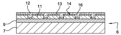
본 발명은 마이크로캐리어(19, 20)를 제조하는 방법으로서, (a) 하부 층(7), 상부 층(8) 및 상기 하부 층(7)과 상기 상부 층(8) 사이에 위치된 절연 층(9)을 포함하는 샌드위치 구조를 갖는 웨이퍼(6)를 제공하는 단계; (b) 상기 마이크로캐리어의 몸체(11)의 측벽(12)의 윤곽을 나타내도록 상기 상부 층(8)을 에칭 제거하는 단계; (c) 상기 몸체(11)의 적어도 상부 표면(14) 상에 제1 활성 층(13)을 퇴적시키는 단계; (d) 상기 제1 활성 층(13) 위에 연속적인 폴리머 층(16)을 도포하는 단계; (e) 상기 하부 층(7) 및 상기 절연 층(9)을 에칭 제거하는 단계; 및 (f) 상기 폴리머 층(16)을 제거하여 상기 마이크로캐리어를 공개시키는 단계를 포함하는, 마이크로캐리어의 제조 방법에 관한 것이다.A method of manufacturing a microcarrier (19,20) comprising the steps of: (a) forming a lower layer (7), an upper layer (8) and an insulating layer Providing a wafer (6) having a sandwich structure including a substrate (9); (b) etching away the top layer (8) to show the contour of the side wall (12) of the body (11) of the microcarrier; (c) depositing a first active layer (13) on at least the upper surface (14) of the body (11); (d) applying a continuous polymer layer (16) over the first active layer (13); (e) etching away the lower layer (7) and the insulating layer (9); And (f) removing the polymer layer (16) to reveal the microcarrier.
Description
본 발명은 마이크로캐리어(microcarrier)를 제조하는 방법 및 마이크로캐리어에 관한 것이다. 본 발명은 특히, 연구 및 임상 검사실용의 생물학적 및/또는 화학적 시금(assay)을 수행하는 데 적합한 마이크로캐리어에 관한 것이다.The present invention relates to a method of manufacturing a microcarrier and a microcarrier. The present invention relates in particular to microcarriers suitable for carrying out biological and / or chemical assays for research and clinical laboratories.
본 발명의 범위 내에서, 마이크로캐리어 또는 극미립자(microparticle)는 임의의 타입의 입자, 각각 일반적으로 최대 치수가 100 ㎚ 내지 300 ㎛, 바람직하게는 1 ㎛ 내지 200 ㎛인 미세한 사이즈의 임의의 타입의 캐리어를 지칭한다.Within the scope of the present invention, microcarriers or microparticles may be of any type of particle size, generally of any of the finer sizes, generally having a maximum dimension of 100 nm to 300 μm, preferably 1 μm to 200 μm Carrier "
본 발명에 따르면, 용어 마이크로캐리어는 기능화된 또는 기능화되도록 설계된, 즉, 마이크로캐리어의 표면에 결합되거나 대량이 함침(impregnate)되는 하나 이상의 리간드(ligand) 또는 기능 유닛을 함유하고 있거나 함유하도록 설계된 극미립자를 지칭한다. 화학적 및 생물학적 분자의 큰 스펙트럼이 마이크로캐리어에 리간드로서 부착(attach)될 수도 있다. 마이크로캐리어는 다수의 기능 및/또는 리간드를 가질 수 있다. 본 명세서에서 사용되는 바와 같이, 용어 기능 유닛은 상기 마이크로캐리어의 표면을 변형하는, 그에 부착하는, 그로부터 첨부하는, 그것을 덮는, 또는 그와 공유 또는 비공유 결합되거나 대량이 함침되는 임의의 종을 규정하는 것을 의미한다. 이들 기능은 고속 대량 스크리닝(high throughput screening) 기술 및 진단에 일상적으로 사용되는 모든 기능을 포함한다.According to the present invention, the term microcarrier is defined as one or more ligands designed to be functionalized or functionalized, i. E. Bound to or impregnated in large amounts on the surface of the microcarrier, or a microparticle containing or containing a functional unit Quot; A large spectrum of chemical and biological molecules may be attached as ligands to the microcarriers. Microcarriers can have multiple functions and / or ligands. As used herein, the term functional unit defines any species that deforms, adheres to, attaches to, covers it with, or is covalently or noncovalently bonded or mass impregnated with the surface of the microcarrier . These functions include high throughput screening techniques and all the functions routinely used for diagnostics.
신약 개발 또는 스크리닝 및 DNA 염기서열 분석은 통상적으로 막대한 수의 화합물 또는 분자에 대해 시금을 수행하는 것을 수반한다. 이들 시금은 일반적으로 예를 들면, 관심 있는 또는 특정 표적 분자의 화합물에 대한 화학적 라이브러리를 스크리닝하는 것, 또는 분자 간의 관심 있는 화학적 및 생물학적 상호 작용에 대해 테스트하는 것을 포함한다. 이들 시금은 종종 수천 가지의 개별적인 화학적 및/또는 생물학적 반응을 수행하는 것을 필요로 한다.New drug development or screening and DNA sequencing typically involve carrying out a large number of compounds or molecules for the assay. These assays generally include, for example, screening a chemical library for a compound of interest or a particular target molecule, or testing for chemical and biological interactions of interest between molecules. These assays often require performing thousands of individual chemical and / or biological reactions.
다수의 현실적인 문제들이 그러한 막대한 수의 개별 반응을 다루는 것으로부터 발생한다. 가장 중대한 문제는 아마도 각각의 개별 반응을 라벨 붙이고 추적할 필요성이다.A number of realistic problems arise from dealing with such a large number of individual responses. Perhaps the most important problem is the need to label and track each individual reaction.
반응의 유사성을 추적하는 하나의 종래의 방법은 마이크로티터 플레이트(microtiter plate)(마이크로어레이(microarray))에서 각 반응을 물리적으로 분리시킴으로써 달성된다. 그러나, 마이크로티터 플레이트의 사용은 특히, 사용되는 마이크로티터 플레이트의 크기 및 그에 따라 마이크로티터 플레이트에서 수행될 수도 있는 상이한 반응의 수에 대한 물리적인 제한 같은 여러 가지 단점을 갖는다.One conventional method of tracking the similarity of reactions is achieved by physically separating each reaction in a microtiter plate (microarray). However, the use of microtiter plates has several disadvantages, in particular, the physical limitations on the size of the microtiter plate used and thus the number of different reactions that may be performed in the microtiter plate.
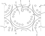
마이크로어레이의 사용에서의 제한에 비추어, 그들 단점은 현재에는 화학적 및/또는 생물학적 시금을 수행하기 위해 기능화된 인코딩된 극미립자로 유리하게 만회된다. 각각의 기능화된 인코딩된 극미립자에는 그 표면에 결합되는 특정 리간드(들)를 고유하게 식별하는 코드가 제공된다. 그러한 기능화된 인코딩된 극미립자의 사용은 랜덤 처리를 가능하게 하며, 이는 수천 개의 고유하게 기능화된 인코딩된 극미립자가 모두 혼합될 수도 있고 동시에 시금 처리될 수도 있음을 의미한다. 기능화된 인코딩된 극미립자의 예들은 국제 특허 출원 WO 00/63695호에 기재되어 있고, 도 1에 도시되어 있다.In view of the limitations in the use of microarrays, their drawbacks are now advantageously retrieved with encoded ultra-fine particles that have been functionalized to perform chemical and / or biological assays. Each functionalized encoded ultra-fine particle is provided with a code that uniquely identifies the particular ligand (s) bound to its surface. The use of such functionalized encoded microparticles allows for random processing, which means that thousands of uniquely functionalized encoded microparticles can be mixed together and processed at the same time. Examples of functionalized encoded ultra fine particles are described in international patent application WO 00/63695 and are shown in FIG.
국제 특허 출원 WO 2010/072011호는 복수의 기능화된 인코딩된 극미립자 또는 마이크로캐리어(1)(도 1)가 팩킹될 수 있는 반응 챔버로서의 역할을 하는 적어도 하나의 마이크로채널을 갖는 시금 디바이스를 기재하고 있다. 미세 유체 채널(microfluidic channel)에는 내부에서 마이크로캐리어(1)를 차단하면서 화학적 및/또는 생물학적 시약을 함유하는 액체 용액이 마이크로채널을 통해 흐를 수 있게 하는 필터로서 작용하는 제한 또는 정지 수단이 제공된다. 상기 미세 유체 채널의 기하학적 높이 및 상기 마이크로캐리어(1)의 치수는 상기 마이크로캐리어(1)가 일반적으로 각 미세 유체 내털 내부에 단층 배열로 배열되도록 하여 상기 마이크로캐리어(1)가 서로 오버랩하는 것을 방지하도록 선택된다.International patent application WO 2010/072011 describes a plurality of functionalized encoded microparticles or a deposition device having at least one microchannel serving as a reaction chamber in which the microcarrier 1 (Fig. 1) can be packed have. The microfluidic channel is provided with a limiting or stopping means which acts as a filter to block the
부착된 리간드(들)과 마이크로채널을 통해 흐르는 화학적 및/또는 생물학적 시약 사이의 관심 있는 유리한 반응을 나타내는 이들 기능화된 인코딩된 마이크로캐리어(1)가 그 후 그들의 코드를 판독할 수도 있으며, 그에 의해 유리한 반응을 생성하는 리간드의 식별을 유도할 수도 있다.These functionalized encoded microcarriers (1), which exhibit an interesting beneficial reaction between the attached ligand (s) and the chemical and / or biological reagents flowing through the microchannels, may then read their codes, Lt; RTI ID = 0.0 > ligand < / RTI > producing the response.
코드는 복수의 횡단 홀(2)의 독특한 패턴을 포함할 수도 있고, 또한 예를 들면, (도 1에 도시된 바와 같은) L 형상 부호(3) 또는 삼각형과 같은 비대칭적인 배향 마크를 포함할 수도 있다. 이 비대칭적인 배향 마크는 마이크로캐리어(1)의 상부 표면(4) 및 하부 표면(5) 사이의 구별을 가능하게 한다.The code may include a unique pattern of a plurality of
용어 마이크로채널 또는 미세 유체 채널은 닫힌 채널, 즉, 현미경 크기 단면을 갖는, 즉, 최소 치수의 단면이 일반적으로 약 1로부터 약 500 ㎛인, 바람직하게는 약 10 내지 200 ㎛인 유체용의 긴 통로를 칭한다. 미세 유체 채널은 반드시 직선일 필요는 없고, 유체가 미세 유체 채널 내에서 흐르는 방향에, 즉, 바람직하게는 층류 체제(laminar flow regime)라고 가정하면 근본적으로 유체의 평균 속도 벡터에 대응하는 방향에 대응하는 길이 방향을 갖는다.The term microchannel or microfluidic channel refers to a closed channel, i. E., A long passage for a fluid having a microscopic size cross-section, i. E., A cross-section with a minimum dimension generally between about 1 and about 500 microns, preferably between about 10 and 200 microns . The microfluidic channel does not necessarily have to be straight and corresponds essentially to the direction corresponding to the mean velocity vector of the fluid, assuming that the fluid flows in the microfluidic channel, i.e., preferably a laminar flow regime. .
WO 2010/072011호에 기재되어 있는 시금 디바이스를 이용하면, 관심 있는 반응의 검출은 도 2에 도시된 바와 같이, 미세 유체 채널 내에 존재하는 각각의 인코딩된 마이크로캐리어(1)의 형광 강도의 연속적인 판독에 의거한 것일 수 있다. 바꿔 말하면, 시금 시에 표적 분자의 존재는 미리 정해진 형광 신호를 트리거(trigger)한다. 그러나, 미리 정해진 형광 신호는 강한 형광 배경의 존재로 인해 검출하기 매우 어려울 수 있다.With the aid of the assay device described in WO 2010/072011, the detection of the reaction of interest can be carried out in succession of the fluorescence intensity of each encoded
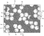
광학 층으로 마이크로캐리어를 코팅하는 것은 시금하는 동안 방출된 형광을 검출 가능한 레벨로 증가시키는 것이 알려져 있다. 예를 들면, 도 2는 문헌 WO 2011/044708호에 기재되어 있는 방법에 의해 수득되는 코팅된 마이크로캐리어(1)의 배치(batch)를 도시하며, 여기에서 광학 층은 마이크로캐리어(1) 상에 퇴적된다.It is known that coating the microcarrier with an optical layer increases the emitted fluorescence to a detectable level during the assay. For example, Figure 2 shows a batch of coated
그러나, 도 2에 예시되는 생물학적 시금의 결과는 코팅된 마이크로캐리어(1)로부터 방출되는 형광 신호의 상이한 패턴을 도시한다. 특히, 일부 마이크로캐리어(1a)는 균일하고 검출 가능한 형광 신호를 방출하는 한편, 다른 마이크로캐리어(1b)는 대부분의 시간에 (이후 "새도우 효과(shadow effect)"라고 칭해지는) 초승달의 형상을 갖는 부분적인 또는 불균일한 형광 신호를 방출한다. 더욱이, 일부 마이크로캐리어는 어떠한 검출 가능한 형광을 방출하지 않는데, 그 이유는 이들 마이크로캐리어가 그 표면 상에 광학 층이 면제되기 때문이다. However, the result of the biological assay illustrated in FIG. 2 shows a different pattern of fluorescence signals emitted from the coated
그러한 결함은 분석하는 동안 정확한 정량적 정보의 추출을 어렵게 만든다.Such defects make it difficult to extract accurate quantitative information during analysis.
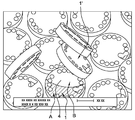
일부 마이크로캐리어(1b) 상의 광학 층의 부재 또는 부분적인 퇴적은 문헌 WO 2011/044708호에 수반되는 프로세스로부터 기인한다. 실제로, 이 프로세스는 광학 층의 퇴적 이전 및 동안에 여러 개의 마이크로캐리어(1) 사이에 부분적인 또는 전체적인 오버래핑(overlapping)을 피할 수 없다. 그러한 오버래핑은 도 3에 도시되어 있으며, 여기에서 마이크로캐리어(1)의 상부 표면(4)의 영역 A는 광학 층에 의해 코팅되는 반면에, 다른 마이크로캐리어(1')에 의해 숨겨지는 상기 마이크로캐리어(1)의 상부 표면(4)의 영역 B는 상기 광학 층에 의해 코팅되지 않는다.The absence or partial deposition of the optical layer on some
더욱이, WO 2011/044708호에 기재되어 있는 프로세스 동안, 여러 개의 마이크로캐리어가 코팅 전에 뒤집힐 수도 있으므로 잘못된 표면 상에 코팅될 수도 있다.Moreover, during the process described in WO 2011/044708, several microcarriers may be coated on the wrong surface as they may be inverted before coating.
또한, 형광 시금을 수행하기 전에 부분적으로 코팅된 마이크로캐리어(1b) 또는 코팅되지 않은 마이크로캐리어를 잘 코팅된 마이크로캐리어(1a)로부터 분리하는 것은 불가능하다. 실제로, 마이크로캐리어 상의 광학 층의 존재는 형광 시금 동안 방출되는 형광 신호에 의해서만 구별될 수 있다.It is also not possible to separate the partially coated
본 발명은 상기 언급한 단점의 전부 또는 일부를 바로잡는 것을 목적으로 한다.The present invention aims at correcting all or part of the above mentioned disadvantages.
이 목적을 위해, 본 발명은 마이크로캐리어를 제조하는 방법으로서, 아래의 단계:For this purpose, the present invention provides a method of manufacturing a microcarrier comprising the steps of:
(a) 하부 층, 상부 층 및 상기 하부 층과 상부 층 사이에 위치하는 절연 층(9)을 포함하는 샌드위치 구조를 갖는 웨이퍼를 제공하는 단계,(a) providing a wafer having a sandwich structure including a lower layer, an upper layer and an insulating layer (9) positioned between the lower layer and the upper layer,
(b) 상기 마이크로캐리어의 몸체의 측벽의 윤곽을 나타내도록 상기 상부 층(8)을 에칭 제거하는 단계,(b) etching away the top layer (8) to reveal contours of the sidewalls of the body of the microcarrier,
(c) 상기 몸체의 적어도 상부 표면 상에 제1 활성 층을 퇴적시키는 단계,(c) depositing a first active layer on at least the upper surface of the body,
(d) 상기 제1 활성 층 위에 연속적인 폴리머 층을 도포하는 단계,(d) applying a continuous polymer layer over the first active layer,
(e) 상기 하부 층 및 상기 절연 층을 에칭 제거하는 단계,(e) etching away the lower layer and the insulating layer,
(f) 상기 마이크로캐리어를 공개시키도록 상기 폴리머 층을 제거하는 단계를 포함하는, 마이크로캐리어의 제조 방법을 제안한다.(f) removing the polymer layer to expose the microcarriers.
그러므로, 본 발명에 따르는 방법에서는, 제1 활성 층의 퇴적은 상술한 플리핑 또는 오버래핑 현상을 방지하기 위해서, 마이크로캐리어가 웨이퍼에 여전히 결속되어 있는 동안 달성된다. 제1 활성 층은 분석하는 동안 상술한 "새도우 효과"를 회피하기 위해 몸체의 전체 상부 표면 상에 균일하게 퇴적된다. 결과적으로, 마이크로채널을 통해 흐르는 리간드(들) 및 표적 분자(들)에 관한 정확한 정량적인 정보에 대한 데이터 무결성이 보존된다.Therefore, in the method according to the present invention, the deposition of the first active layer is achieved while the microcarriers are still bound to the wafer, in order to prevent the above-mentioned flipping or overlapping phenomenon. The first active layer is uniformly deposited on the entire upper surface of the body to avoid the "shadow effect" described above during the analysis. As a result, data integrity for accurate quantitative information about the ligand (s) and target molecule (s) flowing through the microchannel is preserved.
마이크로캐리어는 또한 그들이 공개될 때까지 함께 결속되므로 예를 들어, 터보 펌프(turbo-pump)에서처럼 준비하는 데 사용되는 설비의 민감한 부품에 마이크로캐리어가 확산되는 것을 방지한다.The microcarriers are also tied together until they are released, thereby preventing the microcarriers from diffusing into the sensitive components of the equipment used to prepare, for example, as in a turbo-pump.
임의로, 제1 활성 층의 퇴적 단계 (c)는 상술한 단계 (a)와 (b) 사이에 이루어진다. 변형예에서는, 단계 (a) 내지 (f)는 연속적으로 실시된다.Optionally, a deposition step (c) of the first active layer is carried out between steps (a) and (b) described above. In a variant, steps (a) to (f) are carried out continuously.
일 실시예에 따르면, 단계 (e)는 예를 들면, 에칭 조(bath)를 사용함으로써 상기 하부 층을 선택적으로 에칭하는 제1 에칭에 의해, 그리고 예를 들면, 건식 에칭에 의해 상기 절연 층을 선택적으로 에칭하는 제2 에칭에 의해 행해진다.According to one embodiment, step (e) is performed by a first etching that selectively etches the underlying layer, for example, by using an etch bath, and by a dry etch, for example, And is performed by a second etching for selectively etching.
상기 하부 층이 단결정 실리콘을 포함하는 경우에는, 에칭 조는 수산화 칼슘 조일 수도 있다. 또한, 상기 절연 층이 이산화 실리콘을 포함하는 경우에는, 건식 에칭이 CHF3(fluoroform: 플루오르포름)의 플라즈마 에칭에 의해 또는 CF4의 플라즈마 에칭에 의해 행해질 수 있다.When the lower layer contains monocrystalline silicon, the etching bath may be a calcium hydroxide bath. Further, when the insulating layer contains silicon dioxide, dry etching can be performed by plasma etching of CHF 3 (fluoroform: fluoroform) or plasma etching of CF 4 .
상기 폴리머 층은 또한, 건식 에칭에 의해 제거될 수도 있다. 예를 들면, 폴리머 층이 파릴렌을 포함하는 경우에는, 폴리머 층은 산소 플라즈마에 의해 에칭될 수도 있다.The polymer layer may also be removed by dry etching. For example, if the polymer layer comprises parylene, the polymer layer may be etched by oxygen plasma.
또한, 예를 들어 단계 (b)와 단계 (c) 사이에서 변별적 마크(distinctive mark), 예를 들어 코드가 상기 마이크로캐리어에 새겨질 수도 있다.Also, for example, between step (b) and step (c), a distinctive mark, for example a code, may be engraved in the microcarrier.
동일한 변별적 마크가 복수의 마이크로캐리어에 예를 들면, 동일한 조에 속하는 모든 마이크로캐리어에 의한 것일 수 있다.The same discriminating mark may be for a plurality of microcarriers, for example, all microcarriers belonging to the same group.
그러므로, 시금하는 동안, 상이한 타입의 마이크로캐리어가 동시에 그리고 함께 혼합되어 사용될 수 있으며, 각각의 타입은 그 자신의 변별적 마크를 갖고 하나 이상의 특정 리간드(들)을 지지한다. 이 경우에는, 특정 마크가 시금하는 동안 각각의 마이크로캐리어 및 그에 부착되는 리간드의 타입을 식별하는 것을 가능하게 한다.Thus, during the assay, different types of microcarriers can be used simultaneously and mixed together, each type having its own distinctive mark and supporting one or more specific ligand (s). In this case, it is possible to identify the type of ligand attached to each microcarrier and to which it is attached during the specific marking.
변별적 마크가 제1 활성 층의 퇴적(단계 c) 이전에 새겨지는 경우, 상기 층의 두께 및 상기 변별적 마크의 사이즈는 제1 활성 층을 통해 변별적 마크가 판독될 수 있도록 선택된다.If the distinctive mark is etched prior to the deposition of the first active layer (step c), the thickness of the layer and the size of the distinctive mark are selected such that the distinctive mark can be read through the first active layer.
또한, 상기 하부 층 및/또는 상기 상부 층은 단결정 실리콘을 포함할 수도 있고, 상기 절연 층은 이산화 실리콘을 포함할 수도 있으며, 상기 폴리머 층은 파릴렌(parylen)을 포함할 수도 있다. 다른 실시예에 따르면, 상기 폴리머 층은 지지부를 상기 웨이퍼에 결속시키는 접착제 층이다.The lower layer and / or the upper layer may also comprise monocrystalline silicon, the insulating layer may comprise silicon dioxide, and the polymer layer may comprise parylen. According to another embodiment, the polymer layer is an adhesive layer that binds the support to the wafer.
단결정 실리콘 층은 선택적 수산화 칼슘 조 에칭과 같은 알려진 에칭 방법에 의해 쉽게 그리고 효율적으로 에칭될 수 있다.The single crystal silicon layer can be etched easily and efficiently by known etching methods such as selective calcium hydroxide group etching.
이산화 실리콘을 포함하는 상기 절연 층은 에칭 조를 사용함으로써 상기 하부 층을 에칭하면서 마이크로캐리어를 보호할 수 있다.The insulating layer containing silicon dioxide can protect the microcarrier while etching the lower layer by using an etching bath.
상기 파릴렌 층은 공개시키기 전에 마이크로캐리어를 유지할 수 있는 높은 저항 층이다.The parylene layer is a high resistive layer that can retain microcarriers before being exposed.
웨이퍼에 결속되는 지지부의 사용은 마이크로캐리어를 제조하는 동안 웨이퍼의 취급을 용이하게 하기 위해 향상된 기계적 성질을 제공한다.The use of supports attached to the wafer provides improved mechanical properties to facilitate handling of the wafer during fabrication of the microcarriers.
본 발명의 일 실시예에 따르면, 예를 들면, 단계 (e)와 단계 (f) 사이에서 상기 마이크로캐리어의 몸체의 적어도 하부 표면 상에 제2 활성 층이 퇴적된다.According to an embodiment of the present invention, for example, a second active layer is deposited on at least the lower surface of the body of the microcarrier between step (e) and step (f).
그러한 방법에 의해 생성된 마이크로캐리어는 2개의 반대의 활성 층, 각각 몸체의 상부 표면 상의 제1 활성 층 및 몸체의 하부 표면 상의 제2 활성 층을 포함한다.The microcarriers produced by such methods comprise two opposing active layers, a first active layer on the upper surface of the body and a second active layer on the lower surface of the body, respectively.
상기 제1 활성 층 및/또는 상기 제2 활성 층은 광학적 또는 자기적 성질을 갖는 재료, 다결정 실리콘 및/또는 폴리테트라프루오로에틸렌, 또는 높은 반사율을 갖는 금속 층을 포함할 수도 있다.The first active layer and / or the second active layer may comprise a material having optical or magnetic properties, polycrystalline silicon and / or polytetrafluoroethylene, or a metal layer having a high reflectivity.
광학적 성질을 갖는 재료를 사용하면 마이크로캐리어의 대응하는 표면으로부터 방출되는 형광 신호를 실질적으로 증가시킨다. 자기 성질을 갖는 재료는 예를 들면, 원하는 방향으로 마이크로캐리어를 배향시키는 데 사용될 수 있다. 다결정 실리콘의 사용은 상기 표면 상에 코팅되는 유효 면적을 증가시키기 위해 몸체의 대응하는 표면의 다공성을 증가시킨다. 마지막으로, 폴리테트라플루오르에틸렌은 마이크로캐리어와 시금하는 동안 테스트하는 표면 사이의 마찰을 감소시키기 위해 사용될 수 있다.The use of a material having optical properties substantially increases the fluorescence signal emitted from the corresponding surface of the microcarrier. Materials with magnetic properties can be used, for example, to orient the microcarriers in a desired direction. The use of polycrystalline silicon increases the porosity of the corresponding surface of the body to increase the effective area coated on the surface. Finally, polytetrafluoroethylene can be used to reduce the friction between the microcarrier and the surface being tested during the deposition.
상기 제1 활성 층 및/또는 상기 제2 활성 층은 산화물 또는 질화물, 예를 들어 이산화 실리콘, 또는 금속층을 포함할 수도 있다.The first active layer and / or the second active layer may comprise an oxide or nitride, for example silicon dioxide, or a metal layer.
이산화 실리콘은 몸체의 대응하는 표면을 평활화시키기 위해 그리고 상기 표면 상에서 특정되지 않은 분자의 슬라이딩을 증가시키기 위해 사용될 수도 있다. 상기 표면에 결속되는 분자에 의해 방출되는 특정 신호는 따라서 특정되지 않은 분자에 의해 방출되는 간섭 신호가 상당히 저하되기 때문에 향상된다.The silicon dioxide may be used to smooth the corresponding surface of the body and to increase the sliding of the molecules not specified on the surface. The specific signal emitted by the molecules bound to the surface is therefore improved because the interference signal emitted by the unspecified molecules is significantly reduced.
본 발명은 또한, 본 발명에 따르는 방법에 의해 수득되는 마이크로캐리어로서, 제1 활성 층으로 덮여지는 상부 표면 및 제2 활성 층으로 덮여지는 하부 표면을 갖는 몸체를 포함하는 마이크로캐리어에 관한 것이다.The present invention also relates to a microcarrier obtained by the method according to the invention, comprising a body having a top surface covered by a first active layer and a bottom surface covered by a second active layer.
몸체의 상부 표면 및 하부 표면은 광학적 성질을 갖는 재료를 포함하는 활성 층(광학 층)으로 덮여지고, 신뢰할 수 있는 시금이 어떤 마이크로캐리어의 배향이든 수행될 수 있다.The upper and lower surfaces of the body are covered with an active layer (optical layer) comprising a material having optical properties, and a reliable measurement can be performed on any microcarrier orientation.
본 발명은 첨부하는 도면을 참조하여 비제한적인 예에 의해 이루어진 아래의 설명을 볼 때 본 발명이 더욱 잘 이해될 수 있고 본 발명의 다른 상세, 특징 및 장점이 드러난다.BRIEF DESCRIPTION OF THE DRAWINGS The present invention will be better understood and other details, features and advantages of the invention will be apparent from the following description, made by way of non-limiting example, with reference to the accompanying drawings, in which: FIG.
도 1은 종래 기술에 따르는 마이크로캐리어의 평면 사시도를 예시한다.
도 2는 시금하는 동안 관측되는 종래 기술에 따르는 마이크로캐리어 상으로의 형광 방출을 예시한다.
도 3은 종래 기술에 따르는 제조 방법에서 광학 층의 퇴적 전의 마이크로캐리어의 배치(batch)의 평면 사시도를 예시한다.
도 4 내지 도 12는 본 발명의 일 실시예에 따라 마이크로캐리어를 제조하는 방법의 연속적인 단계를 예시한다.
도 13 내지 도 17은 본 발명의 다른 실시예를 예시한다.
도 18은 시금하는 동안 관측되는 본 발명에 따르는 마이크로캐리어 상으로의 형광 방출을 예시한다.1 illustrates a planar perspective view of a microcarrier according to the prior art.
Figure 2 illustrates fluorescence emission onto microcarriers according to the prior art observed during the assay.
Figure 3 illustrates a planar perspective view of a batch of microcarriers prior to deposition of an optical layer in a manufacturing method according to the prior art.
Figures 4 to 12 illustrate successive steps of a method of fabricating a microcarrier in accordance with an embodiment of the present invention.
13 to 17 illustrate another embodiment of the present invention.
Figure 18 illustrates fluorescence emission onto a microcarrier according to the present invention as observed during the assay.
본 발명에 따르는 마이크로캐리어를 제조하는 방법은 도 6 내지 도 17을 참조하여 기술된다. 이 방법은 아래의 연속적인 단계를 포함한다:A method of manufacturing a microcarrier according to the present invention will be described with reference to Figs. This method includes the following consecutive steps:
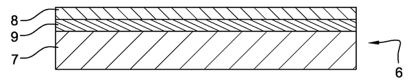
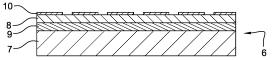
도 4에 도시되어 있는 제1 단계는 하부 층(7), 상부 층(8) 및 상기 하부 층(7)과 상기 상부 층(8) 사이에 위치된 절연 층(9)을 포함하는 샌드위치 구조를 갖는 웨이퍼(6)를 제공하는 것에 있다.The first step shown in Figure 4 is a sandwich structure comprising a
예를 들면, 상기 웨이퍼(6)는 100 ㎜의 직경, 380 ㎛ 두께의 하부 층(7), 1 ㎛ 두께의 절연 층(9) 및 10 ㎛ 두께의 상부 층(8)을 갖는 SOI(Silicon On Insulator: 실리콘 온 절연체) 웨이퍼이다. 상부 층(8) 및 하부 층(7)은 단결정 실리콘으로 만들어지고, 절연 층(9)은 이산화 실리콘으로 만들어진다.For example, the
도 5에 도시되어 있는 제2 단계는 상부 층(8) 상에 감광성 레지스트 층(photosensitive resist layer: 10)을 도포하는 것에 있다. 마이크로캐리어의 표면 레이아웃을 상세하게 기술하기 위해, 감광성 레지스트 층(10)이 크롬/유리 마스크와 같은 마스크(도시 생략)를 통해 UV 광으로 조명된다. 마이크로캐리어 레이아웃에 대응하는 마스크 내의 개방 패턴은 공간 선택적인(space-selective) UV 조명을 제공한다. 광 개시제들이 반응하여 레지스트가 공간 선택적으로 조명된 레지스트 층(10)을 중합시키기 시작한다. 그 후, 노출되지 않고 미반응의 레지스트를 제거하기 위해 특수 화학이 사용된다. 경화된 레지스트의 나머지 패턴은 마이크로캐리어의 외부 형상을 정한다.The second step shown in Figure 5 is to apply a photosensitive resist
본 명세서에서의 바람직한 실시예에서, 경화된 레지스트의 나머지 패턴은 더욱이, 도 1에 도시된 홀(2 및 3)과 유사한 마이크로캐리어의 몸체(11) 내의 일련의 관통 홀로 이루어진 이진 코드와 같은 코드를 정의한다.In the preferred embodiment herein, the remaining pattern of the cured resist further comprises a code such as a binary code consisting of a series of through holes in the
감광성 레지스트(10)는 양의 또는 음의 포토레지스트일 수도 있다. 양의 레지스트의 일례는 쉬플리 컴퍼니(Shipley Company)에 의해 공급되는 MICROPOSIT S 1805 PHOTO RESIST이고, 음의 포토레지스트의 일례는 거스텔텍 엔지니어링 솔루션즈(Gersteltec Engineering Solutions)에 의해 공급되는 GM1040 SU-8 PHOTO EPOXY이다. 감광성 레지스트 층(10)은 스프레이 코팅, 또는 바람직하게는 스핀 코팅과 같은 당업계에 알려져 있는 상이한 기술에 의해 웨이퍼(6) 상에 도포될 수도 있다.The photosensitive resist 10 may be a positive or negative photoresist. One example of a positive resist is MICROPOSIT S 1805 PHOTO RESIST supplied by Shipley Company and an example of negative photoresist is GM1040 SU-8 PHOTO supplied by Gersteltec Engineering Solutions EPOXY. The photosensitive resist
도 6에 도시되어 있는 제3 단계는 마이크로캐리어의 몸체(11)의 측벽(12)의 윤곽을 나타내도록 상부 층(8)을 에칭하는 것에 있다. 이것은 DRIE(Deep Reactive Ion Etching)를 기초로 하는 깊은 실리콘 에칭을 위한 보쉬(Bosch) 프로세스와 같은 심도 반응성 실리콘 에칭(DRIE)에 의해 달성될 수도 있다.The third step shown in Figure 6 is to etch the
보쉬 프로세스는 문헌 "J.K. Bhardwaj, H. Ashraf, Proc. SPIE, 2639, 224 (1995); A. Schilp, M. Hausner, M. Puech, N. Launay, H. Karagoezoglu, F. Laermer, Advanced etch tool for high etch rate deep reactive ion etching in silicon micromachining production environment, Proceeding MST 2001, Dusseldor"에 개시되어 있다. 심도 반응성 이온 에칭은 문헌 "Madou MJ, 2002, Fundamentals of microfabrication, CRC Press"에 개시되어 있다.The Bosch process is described in the article "JK Bhardwaj, H. Ashraf, Proc. SPIE, 2639, 224 (1995); A. Schilp, M. Hausner, M. Puech, N. Launay, H. Karagoezoglu, F. Laermer, " Proceeding MST 2001, Dusseldor "for a high-etch rate deep reactive ion etching in a silicon micromachining production environment. Depth reactive ion etching is described in "Madou MJ, 2002, Fundamentals of microfabrication, CRC Press ".
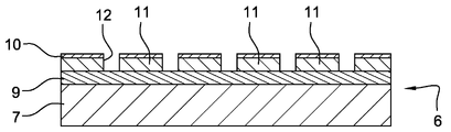
도 7에 도시되어 있는 제4 단계에서는, 감광성 레지스트(10)가 습식 화학 조에서 제거된다. 그러므로, 마이크로캐리어의 설계에 따라서 패터닝되는 일련의 몸체(11)를 정하는 청정의 단결정 실리콘층이 남겨진다.In the fourth step shown in Fig. 7, the photosensitive resist 10 is removed from the wet chemical bath. Therefore, a clean single crystal silicon layer defining a series of
도 8에 도시되어 있는 제5 단계는 몸체(11)의 상부 표면(14) 상에 제1 활성 층(13)을 퇴적하는 것에 있다. 퇴적하는 동안, 제1 활성 층(13)은 또한 측벽(12) 사이에 형성되는 오목부(15)의 하부에 퇴적된다.The fifth step shown in Fig. 8 consists in depositing the first
제1 활성 층(13)은 이산화 실리콘을 포함하는 산화물층과 같은 광학적 성질을 갖는 층이다. 제1 층(13)의 두께는 적색 형광 라벨(label)을 갖고 작동할 때 대략 90 ㎚와 120 ㎚ 사이이다. 질화물과 같은 임의의 다른 유전체 재료, 또는 금속층이 또한 사용될 수도 있다.The first
PECVD(Plasma-enhanced chemical vapor deposition: 플라즈마 강화 화학 기상 증착), 기화, 또는 스퍼터링(Madou MJ, 2002, Fundamentals of microfabrication, CRC Press)과 같은 상이한 타입의 산화물 퇴적 방법이 사용될 수 있다. PECVD 기술로부터 이산화 실리콘의 퇴적을 위해, 디클로로실란 또는 실란과 같은 기체와 산소의 혼합물이 일반적으로 수백 mTorr로부터 수 Torr까지의 압력에서 사용될 수도 있다. 이산화 실리콘의 퇴적은 실온에서부터 300℃까지의 범위 내에 포함되는 온도로 수행된다.Different types of oxide deposition methods may be used, such as PECVD (Plasma Enhanced Chemical Vapor Deposition), vaporization, or sputtering (Madou MJ, 2002, Fundamentals of microfabrication, CRC Press). For the deposition of silicon dioxide from PECVD technology, a mixture of gas and oxygen, such as dichlorosilane or silane, may be used at pressures of typically a few hundreds mTorr to several Torr. Deposition of the silicon dioxide is carried out at a temperature comprised within the range from room temperature to 300 < 0 > C.
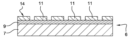
도 9에 도시되어 있는 제6 단계는 제1 활성 층(12) 위에 폴리머 층(16), 예를 들어 회사들 브류어 사이언스, 마이크로케미컬 앤드 올레지스트(Brewer Science, Microchemical and Allresist)에 의해 각각 제공되는 참조물 ProTEK, AZ PC 520D 또는 SX AR-PC 5000/40 하에 알려진 재료로 만들어진 층 또는 파릴렌(parylen) 층을 도포하는 것에 있다. 상기 폴리머 층(16)의 두께는 1㎛와 100㎛ 사이일 수도 있다. 이 폴리머 층은 예를 들면, 화학 기상 증착(CVD)에 의해 또는 스핀 코팅에 의해 도포된다. 도 10에 도시되어 있는 제7 단계는 하부 층(7) 및 절연 층(9)을 에칭 제거하는 것에 있다.The sixth step shown in FIG. 9 is provided on the first
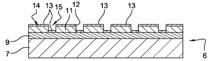
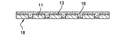
하부 층(7)의 에칭 제거는 하부 층(7)의 대부분을 그라인딩하고 SOI 웨이퍼를 수산화 칼슘 조(bath)에 침지하는 것에 있는 조 에칭(bath etching)에 의해 하부 층(7)의 나머지를 에칭함으로써 수행된다. 그 후, 절연 층(9)이 CHF3(플루오르포름)의 플라즈마 에칭에 의해 또는 CF4의 플라즈마 에칭에 의해 완전히 에칭 제거된다. 절연 층의 예치 비율이 제어된다. 이중층화된(bi-layered) 마이크로캐리어를 생성하기 위해, 본 발명의 제1 실시예에 따르는 방법은 도 11에 도시되어 있는 제8 단계를 포함하며, 이 단계는 마이크로캐리어의 몸체(11)의 하부 표면(18) 상에 제2 활성 층(17)을 퇴적하는 것에 있다. 제2 활성 층(17)은 또한, 이산화 실리콘을 포함하는 산화물 층과 같은 광학적 성질을 갖는다. 제2 층(17)의 두께는 대략 적색 형광 라벨을 갖고 작동할 때 90 ㎚와 120 ㎚ 사이이다. 질화물과 같은 임의의 다른 유전체 재료 또는 금속 층이 또한 사용될 수 있다.The etch removal of the
제2 활성 층(17)은 제1 활성 층(13)의 퇴적에 사용되는 것과 동일한 방법으로 퇴적될 수도 있다.The second
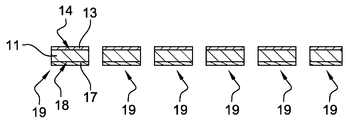
그 후, 폴리머 층(16)이 예를 들면, 산소 플라즈마에 의해 도 12a에 도시된 바와 같이, 이중층화된 마이크로캐리어(19)를 분리시켜 공개시키기 위해 에칭 제거된다. 에치 속도는 제어된다. 그러한 방법에 의해 수득되는 마이크로캐리어(19)는 각각 그 상부 표면(14)에 제1 활성 층(13)을 갖고 그 하부 표면(18) 상에 제2 활성 층(17)을 갖는 몸체(11)를 포함한다. 각 활성 층(13, 17)은 몸체(11)의 대응하는 표면(14, 18)을 균일하고 연속적으로 덮는다.The
도 13 내지 도 17은 본 발명에 따르는 방법의 다른 실시예를 예시한다.Figures 13-17 illustrate another embodiment of a method according to the present invention.
이 실시예에서는, 도 8에 도시되는 웨이퍼(6)가 동일한 5개의 단계에 의해 수득된다.In this embodiment, the
그 후, 제6 단계에서는(도 13), 지지부(21)가 접착제의 층(22)으로 덮여진다. 지지부(21)는 예를 들면, 실리콘, 석영 또는 유리로 만들어진 웨이퍼이고 약 300 ㎛ 내지 700 ㎛의 두께를 갖는다. 접착제는 예를 들면, 회사 브류어 사이언스에 의해 제공되고 WaferBOND HT10.10 또는 CR200로 참조되는 수지이다. 접착제 층(22)의 두께는 약 10 ㎛ 내지 100 ㎛이고, 바람직하게는 약 50 ㎛이다.Thereafter, in a sixth step (Fig. 13), the
도 14에 도시되어 있는 제7 단계에서는, 지지부(21)는 제1 활성 층(13)에 접촉하여 부착되는 접착제 층(22)을 통해 웨이퍼(6)에 결속된다. 그러한 결속은 바람직하게는 웨이퍼(6), 지지부(21) 및 접착제 층(22)을 압축 및 가열함으로써 이루어진다.In the seventh step shown in Fig. 14, the supporting
변형예에서는, 접착제 층(22)이 제1 활성 층(13) 상에 직접 도포되고, 지지부(21)가 접착제 층(22) 상에 도포된다.The
도 15에 도시되어 있는 제8 단계는 하부 층(7) 및 절연 층(9)을 에칭 제거하는 것에 있다. 이 에칭 단계는 도 10에서 수행되는 것과 유사하다.The eighth step shown in Fig. 15 is to etch away the
제2 활성 층(17)이 그 후 마이크로캐리어의 몸체(11)의 하부 표면(18) 상에 퇴적될 수 있다(도 16).A second
그 후, 지지부(21)는 접착제 층(22)을 제거함으로써 웨이퍼(6)로부터 분리된다. 그러한 제거는 용제의 사용에 의해 또는 접착제 층(22)을 가열함으로써 이루어질 수 있다. 그러므로, 도 17에 도시된 바와 같이, 이중층화된 마이크로캐리어(19)가 분리되어 공개된다.Thereafter, the supporting
지지부(21)는 마이크로캐리어를 생성하는 동안 웨이퍼(6)의 취급을 용이하게 하기 위해 향상된 기계적인 성질을 제공한다.The
도 13에 도시된 바와 같이, 시금하는 동안, 각 마이크로캐리어(19)의 기능화된 표면이 균일한 형광 신호를 방출함으로써 상기 언급한 "새도우 효과"가 방지된다. 그러므로, 그러한 마이크로캐리어(19)의 사용은 시금하는 동안 정확한 정량적인 정보를 제공한다.As shown in Fig. 13, during the course of the deposition, the above-mentioned "shadow effect" is prevented by the functionalized surface of each microcarrier 19 emitting a uniform fluorescence signal. Therefore, the use of such a
이중층화된 마이크로캐리어(19)의 사용은 분석하는 동안 마이크로캐리어의 배향을 제어하기 어려울 때 유용하다.The use of a
반대로, 마이크로캐리어의 배향이 제어될 수 있는 경우에는, 몸체(11)의 상부 표면(14)만 활성 층(13)으로 덮여질 수 있다.Conversely, when the orientation of the microcarriers can be controlled, only the
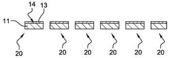
이러한 목적을 위해, 본 발명에 따르는 방법의 다른 실시예는 도 10에 도시되어 있는 제7 단계 직후에 폴리머 층(16)을 에치하도록, 또는 (웨이퍼(6)로부터 지지부(21)를 분리시키기 위해) 도 15에 도시되어 있는 단계와 동시에 접착제 층(22)을 바로 제거하도록 제안한다.For this purpose, another embodiment of the method according to the present invention may be used to etch the
이 실시예에서는, 도 12b에 도시되어 있는 바와 같이, 단 하나의 활성 층(13)을 갖는 마이크로캐리어(20)가 공개된다. 이 실시예는 가격이 덜 비싼 마이크로캐리어(20)의 제조를 인에이블시키는 덜 복잡한 방법을 수반한다.In this embodiment, as shown in Fig. 12B, a
각각의 실시예에서, 공개된 마이크로캐리어(19, 20)는 시금에 사용할 때까지 액체 용기 또는 베셀(vessel) 내에 현탁 상태로 유지될 수도 있다. 각각의 마이크로캐리어(19, 20)는 바람직하게는 디스크의 형태의 형상이고, 1 ㎛와 200 ㎛ 사이의, 예를 들어 40 ㎛의 직경을 갖는다.In each embodiment, the disclosed
본 발명의 다른 실시예들은 본 명세서에 개시되어 있는 발명의 실시 및 명세서의 고려사항으로부터 당업자에게 명백해질 것이다. 명세서 및 실험예는 예시적인 것으로서만 고려되며, 본 발명의 진정한 범위 및 사상은 후속하는 청구항들에 의해 나타내는 것으로 의도된다.Other embodiments of the invention will be apparent to those skilled in the art from consideration of the specification and practice of the invention disclosed herein. It is intended that the specification and examples be considered as exemplary only, with a true scope and spirit of the invention being indicated by the following claims.
Claims (12)
(a) 하부 층(7), 상부 층(8) 및 상기 하부 층(7)과 상기 상부 층(8) 사이에 위치된 절연 층(9)을 포함하는 샌드위치 구조를 갖는 웨이퍼(6)를 제공하는 단계;
(b) 상기 마이크로캐리어(19, 20)의 몸체(11)의 측벽(12)의 윤곽을 나타내도록(delinate) 상기 상부 층(8)을 에칭 제거하는(etching away) 단계;
(c) 상기 몸체(11)의 적어도 상부 표면(14) 상에 제1 활성 층(13)을 퇴적시키는 단계;
(d) 상기 제1 활성 층(13) 위에 연속적인 폴리머 층(16, 22)을 도포하는 단계;
(e) 상기 하부 층(7) 및 상기 절연 층(9)을 에칭 제거하는 단계; 및
(f) 상기 마이크로캐리어(19, 20)를 공개시키도록 상기 폴리머 층(16, 22)을 제거하는 단계
를 포함하는, 마이크로캐리어를 제조하는 방법.In the method for manufacturing the microcarriers (19, 20)
(a) providing a wafer (6) having a sandwich structure comprising a lower layer (7), an upper layer (8) and an insulating layer (9) positioned between the lower layer (7) ;
(b) etching away the top layer (8) to delineate the sidewalls (12) of the body (11) of the microcarriers (19, 20);
(c) depositing a first active layer (13) on at least the upper surface (14) of the body (11);
(d) applying a continuous polymer layer (16, 22) over the first active layer (13);
(e) etching away the lower layer (7) and the insulating layer (9); And
(f) removing the polymer layer (16, 22) to expose the microcarriers (19, 20)
≪ / RTI >
단계 (e)는 예를 들어 에칭 조(bath)를 사용함으로써 상기 하부 층(7)을 선택적으로 에칭하는 제1 에칭에 의해, 그리고 예를 들어 건식 에칭에 의해 상기 절연 층(9)을 선택적으로 에칭하는 제2 에칭에 의해 행해지는 것인, 마이크로캐리어를 제조하는 방법.The method according to claim 1,
Step e) may be carried out by a first etching that selectively etches the underlying layer 7, for example by using an etch bath, and by selectively etching the insulating layer 9, for example by dry etching Wherein the first etch is performed by a second etch that etches the second layer.
상기 폴리머 층(16)은 건식 에칭에 의해 제거되는 것인, 마이크로캐리어를 제조하는 방법.3. The method according to claim 1 or 2,
Wherein the polymer layer (16) is removed by dry etching.
예를 들어 단계 (b)와 단계 (c) 사이에서 변별적 마크(distinctive mark), 예를 들어 코드(2, 3)가 상기 마이크로캐리어(19, 20) 상에 새겨지는 것인, 마이크로캐리어를 제조하는 방법.4. The method according to any one of claims 1 to 3,
For example a distinctive mark, for example code 2, 3, is engraved on the microcarriers 19, 20 between step (b) and step (c) Lt; / RTI >
상기 하부 층(7) 및/또는 상기 상부 층(8)은 단결정 실리콘을 포함하는 것인, 마이크로캐리어를 제조하는 방법.5. The method according to any one of claims 1 to 4,
Wherein the lower layer (7) and / or the upper layer (8) comprise monocrystalline silicon.
상기 절연 층(9)은 이산화 실리콘을 포함하는 것인, 마이크로캐리어를 제조하는 방법.6. The method according to any one of claims 1 to 5,
Wherein the insulating layer (9) comprises silicon dioxide.
상기 폴리머 층(16)은 파릴렌(parylen)을 포함하는 것인, 마이크로캐리어를 제조하는 방법.7. The method according to any one of claims 1 to 6,
Wherein the polymer layer (16) comprises parylene.
상기 폴리머 층은 지지부(21), 예를 들어 실리콘, 석영 또는 유리로 만들어진 웨이퍼를 상기 웨이퍼(6)에 결속시키는 접착제 층(22)인 것인, 마이크로캐리어를 제조하는 방법.The method according to any one of claims 1, 2, and 4 to 6,
Wherein the polymer layer is an adhesive layer (22) that binds a wafer (21), e.g., a wafer made of silicon, quartz or glass, to the wafer (6).
예를 들어 단계 (e)와 단계 (f) 사이에서 상기 마이크로캐리어(19)의 몸체(11)의 적어도 하부 표면(18) 상에 제2 활성 층(17)이 퇴적되는 것인, 마이크로캐리어를 제조하는 방법.9. The method according to any one of claims 1 to 8,
Wherein a second active layer (17) is deposited on at least the lower surface (18) of the body (11) of the microcarrier (19) between steps e) and f) Lt; / RTI >
상기 제1 활성 층(13) 및/또는 상기 제2 활성 층(17)은 광학적 또는 자기적 성질을 갖는 재료, 다결정 실리콘 및/또는 폴리테트라프루오로에틸렌, 또는 높은 반사율을 갖는 금속 층을 포함하는 것인, 마이크로캐리어를 제조하는 방법.10. The method according to any one of claims 1 to 9,
The first active layer 13 and / or the second active layer 17 may comprise a material having optical or magnetic properties, polycrystalline silicon and / or polytetrafluoroethylene, or a metal layer having a high reflectivity ≪ / RTI >
상기 제1 활성 층(13) 및/또는 상기 제2 활성 층(17)은 산화물 또는 질화물, 예를 들어 이산화 실리콘, 또는 금속층을 포함하는 것인, 마이크로캐리어를 제조하는 방법.11. The method according to any one of claims 1 to 10,
Wherein the first active layer (13) and / or the second active layer (17) comprises an oxide or nitride, for example silicon dioxide, or a metal layer.
Applications Claiming Priority (3)
| Application Number | Priority Date | Filing Date | Title |
|---|---|---|---|
| EP12177718.9A EP2690059A1 (en) | 2012-07-24 | 2012-07-24 | Method for producing microcarriers |
| EP12177718.9 | 2012-07-24 | ||
| PCT/EP2013/065442 WO2014016262A1 (en) | 2012-07-24 | 2013-07-22 | Method for producing microcarriers |
Publications (1)
| Publication Number | Publication Date |
|---|---|
| KR20150040939A true KR20150040939A (en) | 2015-04-15 |
Family
ID=48808369
Family Applications (1)
| Application Number | Title | Priority Date | Filing Date |
|---|---|---|---|
| KR20157004439A KR20150040939A (en) | 2012-07-24 | 2013-07-22 | Method for producing microcarriers |
Country Status (13)
| Country | Link |
|---|---|
| US (1) | US9349545B2 (en) |
| EP (2) | EP2690059A1 (en) |
| JP (1) | JP6277188B2 (en) |
| KR (1) | KR20150040939A (en) |
| CN (1) | CN104736470B (en) |
| AU (1) | AU2013295081B2 (en) |
| BR (1) | BR112015001463A2 (en) |
| CA (1) | CA2879150C (en) |
| ES (1) | ES2787857T3 (en) |
| IN (1) | IN2015DN00439A (en) |
| RU (1) | RU2631526C2 (en) |
| WO (1) | WO2014016262A1 (en) |
| ZA (1) | ZA201500438B (en) |
Cited By (1)
| Publication number | Priority date | Publication date | Assignee | Title |
|---|---|---|---|---|
| KR20200101577A (en) | 2019-02-19 | 2020-08-28 | 전남대학교산학협력단 | Microcarrier for Embolization and Preparation Method thereof |
Families Citing this family (3)
| Publication number | Priority date | Publication date | Assignee | Title |
|---|---|---|---|---|
| EP2690058A1 (en) * | 2012-07-24 | 2014-01-29 | Biocartis SA | Method for producing microcarriers and for performing biological assays |
| US9978644B1 (en) * | 2016-09-07 | 2018-05-22 | Amkor Technology, Inc. | Semiconductor device and manufacturing method |
| CN110484129B (en) * | 2019-07-02 | 2022-01-25 | 昆山联滔电子有限公司 | Product with protective coating and preparation method thereof |
Family Cites Families (17)
| Publication number | Priority date | Publication date | Assignee | Title |
|---|---|---|---|---|
| US5071792A (en) * | 1990-11-05 | 1991-12-10 | Harris Corporation | Process for forming extremely thin integrated circuit dice |
| US5545291A (en) * | 1993-12-17 | 1996-08-13 | The Regents Of The University Of California | Method for fabricating self-assembling microstructures |
| NZ515214A (en) | 1999-04-16 | 2003-06-30 | Tibotec Nv | Encoding of microcarriers on or beneath the surface with multiple intensities for higher encoding rate |
| US6963530B1 (en) * | 2000-02-01 | 2005-11-08 | Research Investment Network, Inc. | Near-field optical head system with integrated slider and laser |
| TWI220927B (en) * | 2000-05-12 | 2004-09-11 | Rong-Seng Chang | Method for producing a micro-carrier |
| US6823744B2 (en) * | 2002-01-11 | 2004-11-30 | Honda Giken Kogyo Kabushiki Kaisha | Six-axis force sensor |
| US7872804B2 (en) * | 2002-08-20 | 2011-01-18 | Illumina, Inc. | Encoded particle having a grating with variations in the refractive index |
| JP2004349416A (en) * | 2003-05-21 | 2004-12-09 | Nikon Corp | Method of manufacturing mems |
| US7951580B2 (en) * | 2004-04-21 | 2011-05-31 | The Regents Of The University Of California | Automated, programmable, high throughput, multiplexed assay system for cellular and biological assays |
| US7507638B2 (en) * | 2004-06-30 | 2009-03-24 | Freescale Semiconductor, Inc. | Ultra-thin die and method of fabricating same |
| US7829440B2 (en) * | 2006-08-07 | 2010-11-09 | Semileds Optoelectronics Co. Ltd. | Method of separating semiconductor dies |
| US8883691B2 (en) * | 2007-06-25 | 2014-11-11 | Affymetrix, Inc. | Encoded microparticles |
| US8097926B2 (en) * | 2008-10-07 | 2012-01-17 | Mc10, Inc. | Systems, methods, and devices having stretchable integrated circuitry for sensing and delivering therapy |
| WO2010072011A1 (en) | 2008-12-23 | 2010-07-01 | Biocartis Sa | Assay device and method for performing biological assays |
| WO2010134019A2 (en) * | 2009-05-19 | 2010-11-25 | Ramot At Tel Aviv University Ltd. | Vertical junction pv cells |
| EP2312393A1 (en) * | 2009-10-14 | 2011-04-20 | Biocartis SA | Method for producing microparticles |
| US8953314B1 (en) * | 2010-08-09 | 2015-02-10 | Georgia Tech Research Corporation | Passive heat sink for dynamic thermal management of hot spots |
-
2012
- 2012-07-24 EP EP12177718.9A patent/EP2690059A1/en not_active Withdrawn
-
2013
- 2013-07-22 RU RU2015101761A patent/RU2631526C2/en not_active IP Right Cessation
- 2013-07-22 US US14/414,174 patent/US9349545B2/en active Active
- 2013-07-22 EP EP13739449.0A patent/EP2877423B1/en active Active
- 2013-07-22 JP JP2015523519A patent/JP6277188B2/en not_active Expired - Fee Related
- 2013-07-22 KR KR20157004439A patent/KR20150040939A/en not_active Application Discontinuation
- 2013-07-22 CN CN201380049104.5A patent/CN104736470B/en not_active Expired - Fee Related
- 2013-07-22 CA CA2879150A patent/CA2879150C/en not_active Expired - Fee Related
- 2013-07-22 WO PCT/EP2013/065442 patent/WO2014016262A1/en active Application Filing
- 2013-07-22 BR BR112015001463A patent/BR112015001463A2/en not_active Application Discontinuation
- 2013-07-22 ES ES13739449T patent/ES2787857T3/en active Active
- 2013-07-22 AU AU2013295081A patent/AU2013295081B2/en not_active Ceased
-
2015
- 2015-01-19 IN IN439DEN2015 patent/IN2015DN00439A/en unknown
- 2015-01-21 ZA ZA2015/00438A patent/ZA201500438B/en unknown
Cited By (1)
| Publication number | Priority date | Publication date | Assignee | Title |
|---|---|---|---|---|
| KR20200101577A (en) | 2019-02-19 | 2020-08-28 | 전남대학교산학협력단 | Microcarrier for Embolization and Preparation Method thereof |
Also Published As
| Publication number | Publication date |
|---|---|
| AU2013295081B2 (en) | 2016-10-06 |
| EP2877423B1 (en) | 2020-03-11 |
| JP2015531691A (en) | 2015-11-05 |
| JP6277188B2 (en) | 2018-02-07 |
| CA2879150A1 (en) | 2014-01-30 |
| AU2013295081A1 (en) | 2015-02-05 |
| RU2015101761A (en) | 2016-08-10 |
| ZA201500438B (en) | 2017-11-29 |
| CN104736470B (en) | 2016-08-17 |
| EP2877423A1 (en) | 2015-06-03 |
| IN2015DN00439A (en) | 2015-06-19 |
| RU2631526C2 (en) | 2017-09-25 |
| WO2014016262A1 (en) | 2014-01-30 |
| US9349545B2 (en) | 2016-05-24 |
| EP2690059A1 (en) | 2014-01-29 |
| US20150162141A1 (en) | 2015-06-11 |
| CN104736470A (en) | 2015-06-24 |
| BR112015001463A2 (en) | 2017-07-04 |
| ES2787857T3 (en) | 2020-10-19 |
| CA2879150C (en) | 2020-07-14 |
Similar Documents
| Publication | Publication Date | Title |
|---|---|---|
| JP2002502955A (en) | Virtual wells for high-throughput screening assays | |
| JP6466966B2 (en) | Method for manufacturing spot array substrate | |
| US20040018615A1 (en) | Virtual wells for use in high throughput screening assays | |
| CN102597875A (en) | Method for producing microparticles | |
| KR20150040939A (en) | Method for producing microcarriers | |
| US9333501B2 (en) | Method for producing structured microcarriers | |
| JP4372790B2 (en) | Actuation device with fringed working area, on-chip lab and microsystem | |
| KR101758145B1 (en) | manufacturing method of micro-beads for bioassay and micro-beads for bioassay thereby | |
| US9400275B2 (en) | Method for producing microcarriers and for performing biological assays | |
| KR20110024623A (en) | Spatially separation nano array biochip and method of preparing the same | |
| Choi | Evaporation-Driven Fast Crystallization of 3D Micro-and Nano-particle Assemblies via Micro Mechanical Systems | |
| Xu | Assembly of ordered microsphere arrays: Platforms for microarrays |
Legal Events
| Date | Code | Title | Description |
|---|---|---|---|
| E902 | Notification of reason for refusal | ||
| E601 | Decision to refuse application |