KR20150022918A - Hybrid light bulbs using combinations of remote phosphor leds and direct emitting leds - Google Patents
Hybrid light bulbs using combinations of remote phosphor leds and direct emitting leds Download PDFInfo
- Publication number
- KR20150022918A KR20150022918A KR1020147036689A KR20147036689A KR20150022918A KR 20150022918 A KR20150022918 A KR 20150022918A KR 1020147036689 A KR1020147036689 A KR 1020147036689A KR 20147036689 A KR20147036689 A KR 20147036689A KR 20150022918 A KR20150022918 A KR 20150022918A
- Authority
- KR
- South Korea
- Prior art keywords
- led
- light
- phosphor
- leds
- dichroic reflector
- Prior art date
Links
Images


Classifications
-
- F—MECHANICAL ENGINEERING; LIGHTING; HEATING; WEAPONS; BLASTING
- F21—LIGHTING
- F21K—NON-ELECTRIC LIGHT SOURCES USING LUMINESCENCE; LIGHT SOURCES USING ELECTROCHEMILUMINESCENCE; LIGHT SOURCES USING CHARGES OF COMBUSTIBLE MATERIAL; LIGHT SOURCES USING SEMICONDUCTOR DEVICES AS LIGHT-GENERATING ELEMENTS; LIGHT SOURCES NOT OTHERWISE PROVIDED FOR
- F21K9/00—Light sources using semiconductor devices as light-generating elements, e.g. using light-emitting diodes [LED] or lasers
- F21K9/60—Optical arrangements integrated in the light source, e.g. for improving the colour rendering index or the light extraction
- F21K9/64—Optical arrangements integrated in the light source, e.g. for improving the colour rendering index or the light extraction using wavelength conversion means distinct or spaced from the light-generating element, e.g. a remote phosphor layer
-
- F—MECHANICAL ENGINEERING; LIGHTING; HEATING; WEAPONS; BLASTING
- F21—LIGHTING
- F21V—FUNCTIONAL FEATURES OR DETAILS OF LIGHTING DEVICES OR SYSTEMS THEREOF; STRUCTURAL COMBINATIONS OF LIGHTING DEVICES WITH OTHER ARTICLES, NOT OTHERWISE PROVIDED FOR
- F21V13/00—Producing particular characteristics or distribution of the light emitted by means of a combination of elements specified in two or more of main groups F21V1/00 - F21V11/00
- F21V13/02—Combinations of only two kinds of elements
- F21V13/08—Combinations of only two kinds of elements the elements being filters or photoluminescent elements and reflectors
-
- F—MECHANICAL ENGINEERING; LIGHTING; HEATING; WEAPONS; BLASTING
- F21—LIGHTING
- F21V—FUNCTIONAL FEATURES OR DETAILS OF LIGHTING DEVICES OR SYSTEMS THEREOF; STRUCTURAL COMBINATIONS OF LIGHTING DEVICES WITH OTHER ARTICLES, NOT OTHERWISE PROVIDED FOR
- F21V7/00—Reflectors for light sources
- F21V7/22—Reflectors for light sources characterised by materials, surface treatments or coatings, e.g. dichroic reflectors
- F21V7/28—Reflectors for light sources characterised by materials, surface treatments or coatings, e.g. dichroic reflectors characterised by coatings
- F21V7/30—Reflectors for light sources characterised by materials, surface treatments or coatings, e.g. dichroic reflectors characterised by coatings the coatings comprising photoluminescent substances
-
- H—ELECTRICITY
- H01—ELECTRIC ELEMENTS
- H01L—SEMICONDUCTOR DEVICES NOT COVERED BY CLASS H10
- H01L25/00—Assemblies consisting of a plurality of individual semiconductor or other solid state devices ; Multistep manufacturing processes thereof
- H01L25/03—Assemblies consisting of a plurality of individual semiconductor or other solid state devices ; Multistep manufacturing processes thereof all the devices being of a type provided for in the same subgroup of groups H01L27/00 - H01L33/00, or in a single subclass of H10K, H10N, e.g. assemblies of rectifier diodes
- H01L25/04—Assemblies consisting of a plurality of individual semiconductor or other solid state devices ; Multistep manufacturing processes thereof all the devices being of a type provided for in the same subgroup of groups H01L27/00 - H01L33/00, or in a single subclass of H10K, H10N, e.g. assemblies of rectifier diodes the devices not having separate containers
- H01L25/075—Assemblies consisting of a plurality of individual semiconductor or other solid state devices ; Multistep manufacturing processes thereof all the devices being of a type provided for in the same subgroup of groups H01L27/00 - H01L33/00, or in a single subclass of H10K, H10N, e.g. assemblies of rectifier diodes the devices not having separate containers the devices being of a type provided for in group H01L33/00
- H01L25/0753—Assemblies consisting of a plurality of individual semiconductor or other solid state devices ; Multistep manufacturing processes thereof all the devices being of a type provided for in the same subgroup of groups H01L27/00 - H01L33/00, or in a single subclass of H10K, H10N, e.g. assemblies of rectifier diodes the devices not having separate containers the devices being of a type provided for in group H01L33/00 the devices being arranged next to each other
-
- H—ELECTRICITY
- H01—ELECTRIC ELEMENTS
- H01L—SEMICONDUCTOR DEVICES NOT COVERED BY CLASS H10
- H01L33/00—Semiconductor devices with at least one potential-jump barrier or surface barrier specially adapted for light emission; Processes or apparatus specially adapted for the manufacture or treatment thereof or of parts thereof; Details thereof
- H01L33/44—Semiconductor devices with at least one potential-jump barrier or surface barrier specially adapted for light emission; Processes or apparatus specially adapted for the manufacture or treatment thereof or of parts thereof; Details thereof characterised by the coatings, e.g. passivation layer or anti-reflective coating
- H01L33/46—Reflective coating, e.g. dielectric Bragg reflector
-
- F—MECHANICAL ENGINEERING; LIGHTING; HEATING; WEAPONS; BLASTING
- F21—LIGHTING
- F21V—FUNCTIONAL FEATURES OR DETAILS OF LIGHTING DEVICES OR SYSTEMS THEREOF; STRUCTURAL COMBINATIONS OF LIGHTING DEVICES WITH OTHER ARTICLES, NOT OTHERWISE PROVIDED FOR
- F21V13/00—Producing particular characteristics or distribution of the light emitted by means of a combination of elements specified in two or more of main groups F21V1/00 - F21V11/00
- F21V13/12—Combinations of only three kinds of elements
-
- F—MECHANICAL ENGINEERING; LIGHTING; HEATING; WEAPONS; BLASTING
- F21—LIGHTING
- F21V—FUNCTIONAL FEATURES OR DETAILS OF LIGHTING DEVICES OR SYSTEMS THEREOF; STRUCTURAL COMBINATIONS OF LIGHTING DEVICES WITH OTHER ARTICLES, NOT OTHERWISE PROVIDED FOR
- F21V7/00—Reflectors for light sources
- F21V7/22—Reflectors for light sources characterised by materials, surface treatments or coatings, e.g. dichroic reflectors
-
- F—MECHANICAL ENGINEERING; LIGHTING; HEATING; WEAPONS; BLASTING
- F21—LIGHTING
- F21Y—INDEXING SCHEME ASSOCIATED WITH SUBCLASSES F21K, F21L, F21S and F21V, RELATING TO THE FORM OR THE KIND OF THE LIGHT SOURCES OR OF THE COLOUR OF THE LIGHT EMITTED
- F21Y2113/00—Combination of light sources
- F21Y2113/10—Combination of light sources of different colours
- F21Y2113/13—Combination of light sources of different colours comprising an assembly of point-like light sources
- F21Y2113/17—Combination of light sources of different colours comprising an assembly of point-like light sources forming a single encapsulated light source
-
- F—MECHANICAL ENGINEERING; LIGHTING; HEATING; WEAPONS; BLASTING
- F21—LIGHTING
- F21Y—INDEXING SCHEME ASSOCIATED WITH SUBCLASSES F21K, F21L, F21S and F21V, RELATING TO THE FORM OR THE KIND OF THE LIGHT SOURCES OR OF THE COLOUR OF THE LIGHT EMITTED
- F21Y2115/00—Light-generating elements of semiconductor light sources
- F21Y2115/10—Light-emitting diodes [LED]
-
- H—ELECTRICITY
- H01—ELECTRIC ELEMENTS
- H01L—SEMICONDUCTOR DEVICES NOT COVERED BY CLASS H10
- H01L2924/00—Indexing scheme for arrangements or methods for connecting or disconnecting semiconductor or solid-state bodies as covered by H01L24/00
- H01L2924/0001—Technical content checked by a classifier
- H01L2924/0002—Not covered by any one of groups H01L24/00, H01L24/00 and H01L2224/00
-
- H—ELECTRICITY
- H01—ELECTRIC ELEMENTS
- H01L—SEMICONDUCTOR DEVICES NOT COVERED BY CLASS H10
- H01L33/00—Semiconductor devices with at least one potential-jump barrier or surface barrier specially adapted for light emission; Processes or apparatus specially adapted for the manufacture or treatment thereof or of parts thereof; Details thereof
- H01L33/48—Semiconductor devices with at least one potential-jump barrier or surface barrier specially adapted for light emission; Processes or apparatus specially adapted for the manufacture or treatment thereof or of parts thereof; Details thereof characterised by the semiconductor body packages
- H01L33/50—Wavelength conversion elements
-
- H—ELECTRICITY
- H01—ELECTRIC ELEMENTS
- H01L—SEMICONDUCTOR DEVICES NOT COVERED BY CLASS H10
- H01L33/00—Semiconductor devices with at least one potential-jump barrier or surface barrier specially adapted for light emission; Processes or apparatus specially adapted for the manufacture or treatment thereof or of parts thereof; Details thereof
- H01L33/48—Semiconductor devices with at least one potential-jump barrier or surface barrier specially adapted for light emission; Processes or apparatus specially adapted for the manufacture or treatment thereof or of parts thereof; Details thereof characterised by the semiconductor body packages
- H01L33/58—Optical field-shaping elements
- H01L33/60—Reflective elements
Abstract
일반 조명 응용에 적합한 광원이 적어도 하나의 원격 인광체 LED와 적어도 하나의 직접 방출 LED를 단일 유닛으로 조합한다. 원격 인광체 LED 및 직접 방출 LED 둘 모두는 기부에 의해 지지되고, 광-확산성일 수 있는 벌브 또는 다른 적합한 커버 부재에 의해 덮인다. 원격 인광체 LED는 제1 LED, 인광체 층, 및 제1 이색성 반사기를 포함한다. 제1 LED로부터의 여기 광이 제1 이색성 반사기에 의해 인광체 층 상으로 반사되어, 제1 이색성 반사기에 의해 실질적으로 투과되는 인광체 광을 생성한다. 직접 방출 LED로부터의 적어도 일부의 광이 제1 이색성 반사기를 포함한 임의의 이색성 반사기를 통과함이 없이 커버 부재로 전파된다. 광원은 비교적 소량의 인광체 재료를 사용하여 백색 광 출력을 제공할 수 있다.A light source suitable for general illumination applications combines at least one remote phosphor LED and at least one direct emitting LED into a single unit. Both the remote phosphor LED and the direct emitting LED are supported by the base and covered by a bulb or other suitable cover member which may be light-diffusing. The remote phosphor LED comprises a first LED, a phosphor layer, and a first dichroic reflector. The excitation light from the first LED is reflected by the first dichroic reflector onto the phosphor layer to produce phosphorescent light that is substantially transmitted by the first dichroic reflector. At least some of the light from the direct emitting LED is propagated to the cover member without passing through any dichroic reflector including the first dichroic reflector. The light source can provide a white light output using a relatively small amount of phosphor material.
Description
본 발명은 일반적으로 광원에 관한 것으로, 특히 발광 다이오드(LED) 및 인광체(phosphor)를 포함하는 고체 광원(solid state light source)에 대한 응용에 관한 것이다. 본 발명은 또한 관련 물품, 시스템 및 방법에 관한 것이다.BACKGROUND OF THE INVENTION 1. Field of the Invention The present invention relates generally to a light source, and more particularly to an application to a solid state light source including a light emitting diode (LED) and a phosphor. The present invention also relates to related articles, systems and methods.
광대역 광을 방출하는 고체 광원이 알려져 있다. 일부 경우에, 그러한 광원은 청색 LED 상에 황색-방출 인광체의 층을 도포함으로써 만들어진다. 청색 LED로부터의 광이 인광체 층을 통과할 때, 청색 광의 일부가 흡수되고, 흡수된 에너지의 상당 부분이 가시 스펙트럼 내의 보다 긴 파장들에서 스토크스-이동된(Stokes-shifted) 광, 전형적으로는 황색 광으로서 인광체에 의해 재방출된다. 인광체 두께는, 청색 LED 광의 일부가 인광체 층을 도중 내내 통과하고 인광체로부터의 황색 광과 조합되어 백색 외양을 갖는 광대역 출력 광을 제공하기에 충분히 작다.Solid-state light sources that emit broadband light are known. In some cases, such a light source is made by applying a layer of yellow-emitting phosphors on a blue LED. When light from the blue LED passes through the phosphor layer, a portion of the blue light is absorbed and a significant portion of the absorbed energy is Stokes-shifted light at longer wavelengths in the visible spectrum, typically And is re-emitted by the phosphor as yellow light. The phosphor thickness is small enough for a portion of the blue LED light to pass all the way through the phosphor layer and to combine with the yellow light from the phosphor to provide broadband output light having a white appearance.
다른 LED-펌핑식 인광체 광원이 또한 제안되었다. 미국 특허 제7,091,653호(오우더커크(Ouderkirk) 등)에서는, LED로부터의 자외(UV) 광이 롱-패스 반사기(long-pass reflector)에 의해 인광체 층 상으로 반사되는 광원이 논의되어 있다. 인광체 층은 가시(바람직하게는, 백색)광을 방출하며, 이 광은 롱-패스 반사기에 의해 실질적으로 투과된다. LED, 인광체 층 및 롱-패스 필터는 UV 광이 LED로부터 롱-패스 반사기로 이동할 때, 광이 인광체 층을 통과하지 않도록 하는 방식으로 배열된다.Other LED-pumped phosphor light sources have also been proposed. U.S. Patent No. 7,091,653 (Ouderkirk et al.) Discusses a light source in which ultraviolet (UV) light from an LED is reflected onto a phosphor layer by a long-pass reflector. The phosphor layer emits visible (preferably white) light, which is substantially transmitted by the long-pass reflector. The LED, the phosphor layer and the long-pass filter are arranged in such a way that when the UV light travels from the LED to the long-pass reflector, the light does not pass through the phosphor layer.
본 발명자들은 새로운 계열의 광대역 고체 광원을 개발하였다. 일반적인 조명 응용에서 전구(light bulb)로서 사용하기 위해 제조될 수 있는 이들 광원은 적어도 하나의 원격 인광체 LED와 적어도 하나의 직접 방출 LED를 단일 "하이브리드" 유닛으로 조합한다. 원격 인광체 LED 및 직접 방출 LED 둘 모두는 기부(base)에 의해 지지되고, 광-확산성일 수 있는 벌브(bulb) 또는 다른 적합한 커버 부재에 의해 덮인다. 원격 인광체 LED는 제1 LED, 인광체 층, 및 제1 이색성(dichroic) 반사기를 포함한다. 제1 LED로부터의 여기 광(excitation light)이 제1 이색성 반사기에 의해 인광체 층 상으로 반사되어, 제1 이색성 반사기에 의해 실질적으로 투과되는 인광체 광을 생성한다. 직접 방출 LED로부터의 적어도 일부의 광이 제1 이색성 반사기를 포함한 임의의 이색성 반사기를 통과함이 없이 커버 부재로 전파된다. 광원은 비교적 소량의 인광체 재료를 사용하여 백색 광 출력을 제공할 수 있다.The present inventors have developed a new series of broadband solid state light sources. These light sources, which may be fabricated for use as light bulbs in common lighting applications, combine at least one remote phosphor LED and at least one direct emitting LED into a single "hybrid" unit. Both the remote phosphor LED and the direct emitting LED are supported by a base and covered by a bulb or other suitable cover member which may be light-diffusing. The remote phosphor LED comprises a first LED, a phosphor layer, and a first dichroic reflector. An excitation light from the first LED is reflected by the first dichroic reflector onto the phosphor layer to produce phosphorescent light that is substantially transmitted by the first dichroic reflector. At least some of the light from the direct emitting LED is propagated to the cover member without passing through any dichroic reflector including the first dichroic reflector. The light source can provide a white light output using a relatively small amount of phosphor material.
본 발명자들은 본 명세서에서, 특히 기부, 기부에 부착되는 광-투과성 커버 부재, 제1 LED, 제2 LED, 제1 인광체 층, 및 기부에 의해 지지되고 커버 부재에 의해 덮이는 제1 이색성 반사기를 포함하며 광대역 출력 광을 방출하는 하이브리드 광원을 기술한다. 제1 이색성 반사기는 제1 LED로부터의 적어도 일부의 여기 광을 제1 인광체 층 상으로 반사하여 제1 인광체 층이 제1 인광체 광을 방출하게 하도록 구성된다. 제1 이색성 반사기는 또한 제1 인광체 광을 실질적으로 투과시키도록 구성된다. 제2 LED는 제1 이색성 반사기를 포함한 임의의 이색성 반사기를 통과함이 없이 제2 LED로부터 커버 부재로 전파되는 적어도 일부의 광을 방출하도록 배치된다. 광원은 또한 제1 및 제2 LED들을 각각 제1 및 제2 구동 신호들로 제어하도록 구성되는 제어기를 포함할 수 있다.The present inventors have described herein, in particular, a light-transmissive cover member attached to a base, a base, a first LED, a second LED, a first phosphor layer, and a first dichroic Describes a hybrid light source that includes a reflector and emits a broadband output light. The first dichroic reflector is configured to reflect at least some of the excitation light from the first LED onto the first phosphor layer to cause the first phosphor layer to emit the first phosphor light. The first dichroic reflector is also configured to substantially transmit the first phosphor light. The second LED is arranged to emit at least a portion of the light propagating from the second LED to the cover member without passing through any dichroic reflector including the first dichroic reflector. The light source may also include a controller configured to control the first and second LEDs with first and second drive signals, respectively.
제1 LED, 제1 인광체 층 및 제1 이색성 반사기는 적어도 일부의 여기 광이 제1 인광체 층을 통과함이 없이 제1 LED로부터 제1 이색성 반사기로 전파되도록 배치될 수 있다. 광원에 의해 방출된 광대역 출력 광은 통상의 관찰자에게 외양이 실질적으로 백색일 수 있다. 제1 LED는 340 내지 480 nm, 또는 400 내지 470 nm의 피크 파장을 갖는 광을 방출할 수 있다.The first LED, the first phosphor layer, and the first dichroic reflector may be arranged to propagate at least some of the excitation light from the first LED to the first dichroic reflector without passing through the first phosphor layer. The broadband output light emitted by the light source may be substantially white in appearance to a typical observer. The first LED may emit light having a peak wavelength of 340 to 480 nm, or 400 to 470 nm.
제2 LED는 복수의 비-펌프(non-pump) LED들 중 하나일 수 있다. 비-펌프 LED는 445 내지 500 nm의 범위 내의 피크 파장을 갖는 청색-방출 LED와, 600 내지 650 nm의 범위 내의 피크 파장을 갖는 적색-방출 LED를 포함할 수 있다.The second LED may be one of a plurality of non-pump LEDs. The non-pump LED may include a blue-emitting LED having a peak wavelength in the range of 445 to 500 nm and a red-emitting LED having a peak wavelength in the range of 600 to 650 nm.
커버 부재는 광-확산성일 수 있고, 오목할 수 있다. 제1 이색성 반사기는 오목할 수 있고, 제1 LED 및 제1 인광체 층 둘 모두를 덮을 수 있다. 광원에 의해 방출된 광대역 출력 광은 실질적으로 백색일 수 있고, 80 이상의 연색 평가 지수(color rendering index)를 가질 수 있다.The cover member may be light-diffusing and may be concave. The first dichroic reflector may be concave and may cover both the first LED and the first phosphor layer. The broadband output light emitted by the light source may be substantially white and may have a color rendering index of 80 or greater.
제1 LED는 복수의 펌프 LED들 중 하나일 수 있다. 또한, 제1 인광체 층은 복수의 인광체들 층 중 하나일 수 있고, 제1 이색성 반사기는 복수의 이색성 반사기들 중 하나일 수 있다. 이색성 반사기들 각각은 펌프 LED들 중 적어도 하나로부터의 여기 광을 인광체 층들 중 대응하는 인광체 층 상으로 반사하도록 구성될 수 있다. 펌프 LED들 각각은 주 방출 표면적을 갖는 주 방출 표면을 구비할 수 있으며, 주 방출 표면적들의 합은 집합 LED 표면적(ALED)이다. 또한, 인광체 층들 각각은 광이 입사하는 주 표면을 구비할 수 있으며, 인광체 입사 표면적들의 합은 집합 인광체 표면적(Aphosphor)이다. Aphosphor/ALED 비는 50, 또는 20, 또는 15, 또는 10, 또는 5, 또는 2 이하일 수 있다.The first LED may be one of a plurality of pump LEDs. Also, the first phosphor layer may be one of a plurality of layers of phosphors, and the first dichroic reflector may be one of a plurality of dichroic reflectors. Each of the dichroic reflectors may be configured to reflect the excitation light from at least one of the pump LEDs onto a corresponding phosphor layer of the phosphor layers. Each of the pump LEDs may have a primary emission surface with a primary emission surface area, and the sum of the primary emission surface areas is an aggregate LED surface area (ALED). Further, each of the phosphor layers may have a major surface on which light is incident, and the sum of the phosphor incident surface areas is an aggregate phosphor surface area (Aphosphor). The Aphosphor / ALED ratio may be 50, or 20, or 15, or 10, or 5, or 2 or less.
본 발명자들은 또한, 제1 LED, 제2 LED 및 제1 인광체 층을 제공하는 단계; 및 제1 LED로부터의 적어도 일부의 여기 광을 가로채도록 그리고 그러한 여기 광을 제1 인광체 층 상으로 반사하여 제1 인광체 층이 제1 인광체 광을 방출하게 하도록, 제1 이색성 반사기를 배열하는 단계를 포함하는 방법을 기술한다. 이 방법은 또한, 제1 인광체 광을 제1 이색성 반사기를 통해 실질적으로 투과시키는 단계; 및 광대역 출력 광을 제공하기 위해, 제1 이색성 반사기를 통해 투과된 제1 인광체 광을 제1 이색성 반사기를 포함한 임의의 이색성 반사기를 통과하지 않은 제2 LED에 의해 방출된 LED 광과 조합하는 단계를 포함할 수 있다.The present inventors have also found that providing a light emitting device comprising: providing a first LED, a second LED and a first phosphor layer; And arranging the first dichroic reflector so as to intercept at least a portion of the excitation light from the first LED and to reflect such excitation light onto the first phosphor layer to cause the first phosphor layer to emit the first phosphor light A method comprising the steps of: The method also includes substantially transmitting the first phosphor light through the first dichroic reflector; And combining the first phosphor light transmitted through the first dichroic reflector with the LED light emitted by the second LED not passing through any dichroic reflector including the first dichroic reflector, to provide broadband output light .
이 방법에서, 제공하는 단계는 복수의 펌프 LED들을 제공하는 단계를 포함할 수 있으며, 복수의 펌프 LED들은 제1 LED와 제3 LED를 포함한다. 일부 경우에, 제1 이색성 반사기는 또한, 제3 LED로부터의 적어도 일부의 여기 광을 가로채도록 그리고 그러한 여기 광을 제1 인광체 층 상으로 반사하여 제1 인광체 층이 제1 인광체 광을 더 많이 방출하게 하도록 배열될 수 있다. 제공하는 단계는 또한 제2 인광체 층을 제공하는 단계를 포함할 수 있고, 이 방법은 제3 LED로부터의 적어도 일부의 여기 광을 가로채도록 그리고 그러한 여기 광을 제2 인광체 층 상으로 반사하여 제2 인광체 층이 제2 인광체 광을 방출하게 하도록, 제2 이색성 반사기를 배열하는 단계를 포함할 수 있다. 조합하는 단계는 광대역 출력 광을 제공하기 위해, 제2 이색성 반사기를 통해 투과된 제2 인광체 광을 제1 이색성 반사기를 통해 투과된 제1 인광체 광 및 임의의 이색성 반사기를 통과하지 않은 제2 LED에 의해 방출된 LED 광과 조합하는 단계를 포함할 수 있다.In this method, the providing step may comprise providing a plurality of pump LEDs, wherein the plurality of pump LEDs comprise a first LED and a third LED. In some cases, the first dichroic reflector may also be configured to intercept at least a portion of the excitation light from the third LED and to reflect such excitation light onto the first phosphor layer such that the first phosphor layer Or more. The providing step may also include providing a second phosphor layer, the method comprising reflecting at least a portion of the excitation light from the third LED and reflecting such excitation light onto the second phosphor layer, And arranging the second dichroic reflector so that the two-phosphor layer emits the second phosphor light. The combining step includes combining the second phosphor light transmitted through the second dichroic reflector with the first phosphor light transmitted through the first dichroic reflector and the second phosphor light transmitted through the dichroic reflector Lt; RTI ID = 0.0 > LED < / RTI >
제2 LED를 제공하는 단계는 복수의 비-펌프 LED들을 제공하는 단계를 포함할 수 있고, 복수의 비-펌프 LED들은 제2 LED와 제4 LED를 포함하며, 광대역 출력 광은 또한 임의의 이색성 반사기를 통과하지 않은 제4 LED에 의해 방출된 LED 광을 포함할 수 있다.The step of providing a second LED may include providing a plurality of non-pump LEDs, wherein the plurality of non-pump LEDs include a second LED and a fourth LED, And the LED light emitted by the fourth LED not passing through the reflector.
관련 방법, 시스템 및 물품이 또한 논의된다.Related methods, systems and articles are also discussed.
본 출원의 이들 태양 및 다른 태양이 이하의 상세한 설명으로부터 명백해질 것이다. 그러나, 어떠한 경우에도 상기의 개요는 청구된 기술적 요지에 대한 제한으로서 해석되어서는 안되며, 그 기술적 요지는 절차를 수행하는 동안 보정될 수도 있는 첨부된 특허청구범위에 의해서만 한정된다.These and other aspects of the present application will become apparent from the following detailed description. In all cases, however, the above summary should not be construed as limiting the claimed subject matter, but the technical spirit of the invention is limited only by the appended claims, which may be amended during the course of the procedure.
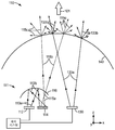
<도 1>
도 1은 원격 인광체 LED와 직접 방출 LED를 조합한 광대역 광원의 개략 측면도 또는 단면도.
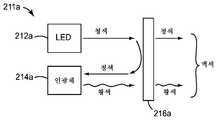
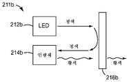
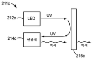
<도 2a 내지 도 2d>
도 2a 내지 도 2d는 주어진 원격 인광체 LED에 사용될 수 있는 일부의 상이한 색상 또는 파장 조합들을 보여주는 기능도.
<도 3>
도 3은 원격 인광체 LED의 개략 사시도.
<도 4>
도 4는 다른 원격 인광체 LED의 개략 사시도.
<도 5>
도 5는 수 개의 원격 인광체 LED들과 수 개의 직접 방출 LED들을 조합한 광대역 광원의 개략 사시도.
<도 6>
도 6은 수 개의 원격 인광체 LED들과 수 개의 직접 방출 LED들을 조합한 다른 광대역 광원의 개략 측면도 또는 단면도.
<도 6a>
도 6a는 도 6의 광원에 사용된 원격 인광체 LED의 개략 측면도 또는 단면도.
<도 7>
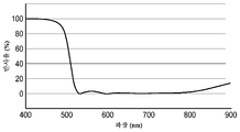
도 7은 이색성 반사기에 대한 스펙트럼 반사율의 그래프.
<도 8>
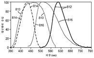
도 8은 원격 인광체 LED에 사용하기 위한 두 인광체 재료들의 스펙트럼 특성의 그래프.
<도 9 내지 도 12>
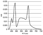
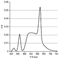
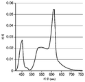
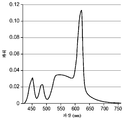
도 9 내지 도 12는 4개의 상이한 시뮬레이션된 광대역 광원들에 대한 스펙트럼 파워 출력의 그래프.
<도 13 내지 도 15>
도 13 내지 도 15는 광대역 광을 제공하는 3개의 상이한 시뮬레이션된 기준 장치들에 대한 스펙트럼 파워 출력의 그래프.
도면들에서, 동일한 도면 부호는 동일한 요소를 지시한다.≪ 1 >
BRIEF DESCRIPTION OF THE DRAWINGS Figure 1 is a schematic side or sectional view of a broadband light source combining a remote phosphor LED and a direct emitting LED.
2A to 2D,
Figures 2a-2d are functional diagrams illustrating some of the different color or wavelength combinations that may be used for a given remote phosphor LED.
3,
3 is a schematic perspective view of a remote phosphor LED;
<Fig. 4>
4 is a schematic perspective view of another remote phosphor LED;
5,
5 is a schematic perspective view of a broadband light source combining several remote phosphor LEDs and several direct emitting LEDs.
6,
6 is a schematic side or cross-sectional view of another broadband light source combining several remote phosphor LEDs and several direct-emitting LEDs.
6A,
6A is a schematic side view or cross-sectional view of the remote phosphor LED used in the light source of FIG. 6;
7,
Figure 7 is a graph of spectral reflectance for a dichroic reflector.
8,
Figure 8 is a graph of the spectral characteristics of two phosphor materials for use in a remote phosphor LED.
<Figs. 9 to 12>
Figures 9-12 are graphs of spectral power output for four different simulated broadband light sources.
<Figs. 13 to 15>
13-15 are graphs of spectral power output for three different simulated reference devices providing broadband light.
In the drawings, the same reference numerals indicate the same elements.
본 발명자들은 하나 이상의 원격 인광체 LED의 광 출력과 하나 이상의 직접 방출 LED의 광 출력을 조합함으로써 특히 유익한 설계 특징을 갖는 광대역 고체 광원이 구성될 수 있는 것을 알았다. 생성된 하이브리드 광원은 강건한 고체 설계를 가질 수 있고, LED와 인광체 재료를 효율적으로 이용할 수 있다. 광원은 또한 높은 연색 평가 지수(CRI)와 같은 바람직한 특성을 백색 광 출력에 제공할 수 있다. 광원은 일반적인 조명 응용에서 전구로서 사용될 수 있거나, 다른 보다 전문화된 응용에서 사용될 수 있다.The inventors have found that a broadband solid state light source with particularly advantageous design features can be constructed by combining the light output of one or more remote phosphor LEDs with the light output of one or more direct emitting LEDs. The resulting hybrid light source can have a robust solid design and can efficiently utilize LED and phosphor materials. The light source may also provide desirable properties, such as a high CRI, to the white light output. Light sources can be used as light bulbs in general lighting applications or in other more specialized applications.
본 출원에서, "발광 다이오드" 또는 "LED"는 가시선이든, 자외선이든 또는 적외선이든 간에, 광을 방출하는 다이오드를 지칭하지만, 많은 실제적인 실시 형태에서, 방출된 광은 약 340 내지 650 ㎚, 또는 약 400 내지 650 ㎚ 범위의 피크 파장을 가질 것이다. LED라는 용어는 수직 공동(cavity) 표면 발광 레이저(vertical cavity surface emitting laser, VCSEL)를 포함하지만 이로 한정되지 않는 레이저 다이오드와 같은 간섭성 반도체 장치뿐만 아니라, 종래의 것이든 초복사형(super radiant variety)이든, "LED"로서 판매되는 비간섭성의 매립된 또는 봉지된 반도체 장치를 포함한다. "LED 다이"는 그의 가장 기본적인 형태, 즉 반도체 처리 절차에 의해 제조된 개별 구성요소 또는 칩 형태의 LED이다. 예를 들어, LED 다이는 하나 이상의 III족 원소들과 하나 이상의 V족 원소들의 조합(III-V족 반도체)으로부터 형성될 수 있다. 적합한 III-V 반도체 재료의 예는 갈륨 질화물과 같은 질화물, 및 인듐 갈륨 인화물과 같은 인화물을 포함한다. 주기율표의 다른 족의 무기 재료뿐만 아니라 다른 유형의 III-V족 재료가 또한 사용될 수 있다. 이 구성 요소 또는 칩은 장치에 동력을 공급하기 위한 전력의 인가에 적합한 전기 접촉부를 포함할 수 있다. 예에는 와이어 본딩(wire bonding), 테이프 자동 본딩(tape automated bonding, TAB), 또는 플립칩 본딩(flip-chip bonding)이 포함된다. 구성요소 또는 칩의 개개의 층 및 다른 기능 요소는 전형적으로 웨이퍼 규모로 형성되고, 완성된 웨이퍼는 이어서 개별적인 단품(piece part)으로 절단되어 다수의 LED 다이가 얻어질 수 있다. LED 다이는 표면 실장, 칩 온 보드(chip-on-board) 또는 기타 공지된 실장 구성용으로 구성될 수 있다. 일부 패키징된 LED는 LED 다이 및 관련 반사기 컵(reflector cup) 위에 중합체 봉지재를 형성함으로써 제조된다. LED는 몇몇 기재들 중 하나의 기재 상에서 성장될 수 있다. 예를 들어, GaN LED는 사파이어, 규소, 및 질화갈륨 상에서 에피택시(epitaxy)에 의해 성장될 수 있다. 이러한 응용의 목적을 위한 "LED"는 또한, 흔히 OLED로 지칭되는 유기 발광 다이오드를 포함하는 것으로 고려되어야 한다.In the present application, the term "light emitting diode" or "LED" refers to a diode that emits light, whether visible, ultraviolet or infrared. In many practical embodiments, however, emitted light is about 340 to 650 nm Will have a peak wavelength in the range of about 400 to 650 nm. The term LED refers to a superradiant variety as is conventional, as well as to coherent semiconductor devices such as, but not limited to, vertical cavity surface emitting lasers (VCSELs) Or non-coherent buried or encapsulated semiconductor devices sold as "LEDs ". An "LED die" is its most basic form, an LED in the form of individual components or chips fabricated by semiconductor processing procedures. For example, an LED die may be formed from a combination of one or more Group III elements and one or more Group V elements (III-V semiconductors). Examples of suitable III-V semiconductor materials include nitrides such as gallium nitride, and phosphides such as indium gallium phosphide. Other types of III-V material may be used as well as inorganic materials of other groups of the periodic table. The component or chip may include an electrical contact adapted for application of electrical power to power the device. Examples include wire bonding, tape automated bonding (TAB), or flip-chip bonding. The individual layers and other functional elements of the component or chip are typically formed on a wafer scale, and the finished wafer may then be cut into individual piece parts to obtain a plurality of LED dies. The LED die may be configured for surface mount, chip-on-board, or other known mounting configuration. Some packaged LEDs are fabricated by forming polymer encapsulants over LED die and associated reflector cups. The LED may be grown on a substrate of one of several substrates. For example, GaN LEDs can be grown by epitaxy on sapphire, silicon, and gallium nitride. "LED" for the purpose of this application should also be considered to include organic light emitting diodes, often referred to as OLEDs.
별개의 인광체 재료를 여기시키거나 "펌핑"하기 위해 사용되는 LED는 본 명세서에서 "펌프 LED"로서 지칭될 수 있다. 인광체는 펌프 LED에 의해 방출된 광의 일부 또는 전부를 흡수하고, 흡수된 에너지의 일부를 스토크스-이동된(보다 긴 파장의) 인광체 광으로서 재방출한다. 본 출원의 목적을 위해, 인광체 광은 전형적으로 실질적으로 가시 파장 범위 내에 있고, 펌프 LED로부터의 여기 광은 전형적으로 가시광 스펙트럼(예컨대, 청색-녹색, 청색 또는 보라색)의 단파장 단부에 또는 그 부근에, 또는 근자외선 내에 있다. 별개의 인광체 재료를 여기시키거나 펌핑하기 위해 사용되지는 않는 LED가 본 명세서에서 "비-펌프 LED"로서 지칭될 수 있다. 본 명세서에 사용되는 바와 같은 용어 "원격 인광체 LED"는 적어도 하나의 펌프 LED; 펌프 LED로부터 효과적으로 구조적으로 분리되지만 그에 광학적으로 결합되는 적어도 하나의 인광체 층 또는 몸체; 및 펌프 LED로부터의 광을 인광체로 실질적으로 반사하고 스토크스-이동된 인광체 광을 실질적으로 투과시키는 이색성 반사기를 포함하는 서브시스템을 지칭한다. 바람직하게는, 이들 구성요소는 여기 광이 인광체 층을 통과함이 없이 펌프 LED로부터 이색성 반사기로 전파되도록 배열된다.LEDs used to excite or "pumped" separate phosphor materials may be referred to herein as "pump LEDs. &Quot; The phosphor absorbs some or all of the light emitted by the pump LED and re-emits a portion of the absorbed energy as stokes-shifted (longer wavelength) phosphor light. For purposes of the present application, the phosphor light is typically substantially within the visible wavelength range, and the excitation light from the pump LED is typically incident on or near the short wavelength end of the visible spectrum (e.g., blue-green, blue or purple) , Or near ultraviolet radiation. LEDs that are not used to excite or pump different phosphor materials can be referred to herein as "non-pump LEDs. &Quot; The term "remote phosphor LED" as used herein includes at least one pump LED; At least one phosphor layer or body that is structurally effectively separated from the pump LED but is optically coupled thereto; And a dichroic reflector that substantially reflects light from the pump LED to the phosphor and substantially transmits stokes-shifted phosphor light. Preferably, these components are arranged to propagate from the pump LED to the dichroic reflector without the excitation light passing through the phosphor layer.
도 1은 예시적인 광대역 고체 광원(110)을 대략 개략적인 형태로 도시한다. 광원(110)은 원격 인광체 LED(111), 직접 방출 LED(130) 및 광-투과성 커버 부재(140)를 포함한다. 표기된 구성요소들을 서로에 대해 고정된 공간 위치들에서 유지하여 원하는 광대역 출력 광(101)을 생성하도록 장착 구조체 및 다른 구성요소(도시되지 않음)가 사용된다.Figure 1 illustrates an exemplary broadband solid state
원격 인광체 LED(111)는 적어도 하나의 펌프 LED(112), 적어도 하나의 인광체 층(114) 및 이색성 반사기(116)를 포함하는 조명 서브시스템이다. 펌프 LED(112)는 인광체를 여기시킬 수 있는 광(113a)을 방출한다. 여기 광(113a)의 2개의 광선만이 도면에 도시되어 있지만, 독자는 LED가 통상적으로 광범위한 방향들에 걸쳐(예컨대, 램버시안 분포로) 그리고 파장들의 대역에 걸쳐 여기 광을 방출하는 것을 이해할 것이다. 여기 광(113a)은 전형적으로 가시 광 스펙트럼의 단파장 단부에 또는 그 부근에 또는 근자외선 내에 있다. 예를 들어, 여기 광은 340 내지 480 nm, 또는 400 내지 470 nm의 범위 내의 피크 파장을 가질 수 있다. 하나의 펌프 LED(112)만이 도면에 도시되어 있지만, 본 명세서의 다른 곳에서 논의된 바와 같이 주어진 원격 인광체 LED 서브시스템 내에 하나 초과의 것이 포함될 수 있다. 여기 광(113a)은 반사된 여기 광(113b)으로서 이색성 반사기(116)에 의해 실질적으로 반사된다.The
원격 인광체 LED(111)는 또한 펌프 LED(112)로부터 효과적으로 구조적으로 분리되지만 그에 광학적으로 결합되는 인광체 층(114)을 포함한다. 인광체 층(114)은 입사(반사된) 여기 광(113b)의 일부 또는 전부를 흡수하고, 흡수된 에너지의 일부를 보다 긴 파장의 인광체 광(115a)으로서 재방출한다. 인광체 광(115a)은 전형적으로 인광체 재료에 의해 모든 방향들로 방출되고, 그러한 광 그 자체는 전형적으로 아래에서 추가로 논의되는 바와 같이 광대역이다. 인광체 광(115a)의 일부는 이색성 반사기(116)를 향해 전파된다. 그러한 광은 반사기(116)에 의해 실질적으로 투과되어 투과된 인광체 광(115b)을 생성한다. 일부 경우에, 반사기(116)는 또한 여기 광(113a)의 일부(전형적으로, 작은 부분)를 투과시킬 수 있다. 투과된 인광체 광(115b)뿐만 아니라, 이색성 반사기(116)를 통해 투과되는 펌프 LED(112)로부터의 임의의 광은, 이어서 전방으로 커버 부재(140)로 전파되고, 커버 부재에서 선택적으로 예시된 바와 같이 원하는 정도의 탁도(haze) 또는 산란을 갖고서 인광체 광(115c)으로서 투과된다.The
이색성 반사기(116)는 일부 경우에 일반성을 위해 도 1에 도시되어 있지 않지만 본 명세서의 다른 도면에 도시된 렌즈 부재의 외측 표면에 정합할 수 있다. 이색성 반사기(116)와 외측 렌즈 표면(존재하는 경우)은 펌프 LED(112)에 의해 방출되고 반사기(116)에 의해 반사되는 광이 주로 인광체 층(114) 상으로 지향되도록 오목하고/하거나 만곡된 형상을 가질 수 있다. 이색성 반사기는 예컨대 인광체 층(114)에 충돌하고/하거나 그에 의해 실제로 흡수되는 반사된 여기 광의 양을 최대화시킴으로써 효율을 최대화시키기 위해, 인광체 층(114)에 또는 그 부근에 적어도 펌프 LED(112)의 근사 이미지를 형성하도록 형상화될 수 있다.The
이색성 반사기는 또한 때때로, 이색성 미러 또는 이색성 필터로 지칭된다. 이들 반사기는 일부 광 파장에 대해서는 고 반사율 및 저 투과율을 갖도록, 그리고 다른 광 파장에 대해서는 저 반사율 및 고 투과율을 갖도록 설계된다. 그러한 반사기는 통상적으로, 반사되지 않은 임의의 광이 적어도 가시선 파장, 근적외선 파장 및 근자외선 파장에 걸쳐 실질적으로 투과되도록 무시할만한 흡수를 가지며, 그 역도 마찬가지이다. 그러한 반사기는, 전형적으로 이산화규소와 이산화티타늄의 교번 층들과 같은 큰 굴절률 부정합을 갖는 재료들의 교번적 배열로 광학적으로 얇은 미세 층들의 적층물을 포함하지만, 다른 적합한 무기 또는 유기 재료들이 또한 사용될 수 있다. 그러한 반사기는 유리 또는 다른 적합한 기재 상에, 예컨대 렌즈 부재의 외측 표면 바로 위에, 또는 그러한 표면에 후속적으로 도포될 수 있는 필름 또는 기재 상에, 교번하는 층들의 진공 증착에 의해 제조될 수 있다. 대안적으로, 적합한 반사성 필름이 미국 특허 제5,882,774호(존자(Jonza) 등) 및 제6,783,349호(니빈(Neavin) 등)에 기술된 바와 같은, 교번하는 중합체 재료들의 공압출 및 얻어진 다층 중합체 웨브의 연신을 수반할 수 있는 연속 공정에 의해 제조될 수 있다. 이색성 반사기에 사용되는 재료 및 사용되는 제조 방법에 관계 없이, 반사기에는 파장의 함수로서 원하는 반사 특성을 제공하도록 맞춤되는 미세 층들의 적층물을 위한 층 두께 프로파일이 제공된다. 두께 프로파일은 롱 패스 필터 또는 노치 필터로서 작동하는 이색성 반사기를 제공하도록 맞춤될 수 있으며, 예를 들어 이에 의해 비교적 장파장의 인광체 광은 입사각의 범위에 걸쳐 실질적으로 투과되고, 비교적 단파장의 LED 여기 광은 주로 반사된다. 이색성 반사기는 예를 들어 인광체 광에 대해 50% 이상, 또는 60% 이상, 또는 70% 이상의 투과율을 가질 수 있다. 일부 경우에, 이색성 반사기는 가시 청색 광을 실질적으로 반사시키고, 가시 자홍색광을 실질적으로 투과시킬 수 있다. 일부 경우에, 이색성 반사기는 다층 미러 필름, 반사성 편광기, 및/또는 소정의 파장에서 직교 편광 상태들을 상이하게 반사하는 미러와 같은 부분 편광 반사기이거나, 이들을 포함할 수 있다.Dichroic reflectors are also sometimes referred to as dichroic mirrors or dichroic filters. These reflectors are designed to have high reflectance and low transmittance for some light wavelengths and low reflectance and high transmittance for other light wavelengths. Such a reflector typically has negligible absorption so that any unreflected light is substantially transmissive over at least the line of sight, near-infrared and near-ultraviolet wavelengths, and vice versa. Such reflectors typically include a stack of optically thin microlayers in an alternating arrangement of materials with large refractive index mismatch, such as alternating layers of silicon dioxide and titanium dioxide, although other suitable inorganic or organic materials may also be used . Such a reflector can be fabricated by vacuum deposition of alternating layers on a glass or other suitable substrate, such as a film or substrate that may be applied directly on, or directly onto, the outer surface of the lens member. Alternatively, a suitable reflective film may be prepared by coextrusion of alternating polymeric materials, such as described in U.S. Patent No. 5,882,774 (Jonza et al.) And 6,783,349 (Neavin et al.), Can be produced by a continuous process which can entail stretching. Regardless of the material used in the dichroic reflector and the fabrication method used, the reflector is provided with a layer thickness profile for a laminate of microlayers that is adapted to provide the desired reflective properties as a function of wavelength. The thickness profile can be tailored to provide a dichroic reflector that operates as a long pass filter or notch filter, e.g., whereby relatively long wavelength phosphor light is substantially transmitted over a range of incident angles, and relatively short wavelength LED excitation light Is mainly reflected. The dichroic reflector may have a transmittance of 50% or more, or 60% or more, or 70% or more, for example, with respect to phosphor light. In some cases, the dichroic reflector may substantially reflect visible blue light and substantially transmit visible magenta light. In some cases, the dichroic reflector may be, or may comprise, a multilayer mirror film, a reflective polarizer, and / or a partially polarized reflector such as a mirror that reflects orthogonal polarization states at a given wavelength differently.
이색성 반사기의 반사 특성 및 투과 특성은 전형적으로, 반사기에 충돌하는 광의 입사각이 변함에 따라 변한다. 예를 들어, 이색성 반사기(116)는 반사기에 수직 입사하는 LED 광선에 비해, 반사기에 비스듬히 입사하는 LED 광선에 대해 더 큰 투과율을 가질 수 있다. 이러한 특성은, 통상적으로 양도되고 계류 중인 PCT 특허출원 공개 WO 2012/091973호에서 보다 완전하게 논의된 바와 같이, 렌즈 조립체 아래에 배치된 다수의 LED의 상대 구동 강도를 제어함으로써 그의 출력 색상이 조절될 수 있는 원격 인광체 고체 광원을 제조하는 데 사용될 수 있다.The reflectance and transmission characteristics of a dichroic reflector typically change as the incident angle of light impinging on the reflector changes. For example, the
인광체 층(114)은 형광을 내거나 그렇지 않으면 흡수된 LED 광에 대해 스토크스 이동된 광을 방출하는 하나 이상의 적합한 인광체 재료를 함유한다. 인광체 재료는 바람직하게는, LED가 인광체를 여기시키고, 인광체가 형광을 내게 하거나 달리 인광체 광을 방출하게 할 수 있도록, LED의 방출 스펙트럼과 파장이 겹치는 범위의 광을 흡수한다. 많은 경우에, 소정의 인광체 재료는 전자기 스펙트럼의 자외선, 청색 및/또는 청록색 부분의 광을 흡수할 수 있으며, 가시 또는 근가시(near-visible) 영역의 광을 방출할 수 있다. 방출된 인광체 광은 전형적으로 광대역인데, 예를 들어 100 나노미터 이상의 스펙트럼 폭을 가질 수 있다. 광대역 인광체 광은 연속적인 넓은 대역에 분포될 수 있거나, 이격된 좁은 방출선들의 집합의 경우에서와 같이 스파이크형 분포를 가질 수 있거나, 좁은 방출선 및 연속적인 넓은 대역의 조합일 수 있다. 예시적인 인광체 재료는 공지의 형광 염료 및 인광체를 포함한다. 세륨-도핑 이트륨 알루미늄 가넷(Ce:YAG)이 사용될 수 있는 인광체의 일례이다. 광원의 설계 상세 및 제약에 따라, 다른 희토류 도핑된 가넷 또는 다른 희토류 도핑된 재료, 예컨대 유로퓸- 및/또는 스트론튬-도핑된 실리케이트, 질화물, 및 알루미네이트가 또한 적합할 수 있다. 적합한 인광체 재료는 유기 및 무기 형광 또는 인광 재료, 예를 들어 도핑된 무기 산화물 또는 질화물, 양자점(quantum dot), 및 II-VI 족 및 III-V족 재료를 포함하는 반도체를 포함할 수 있다.
본 명세서에 개시된 인광체 층은, 하나 이상의 유형의 형광 입자, 예컨대 희토류 도핑된 가넷 또는 본 명세서에 언급된 다른 형광 재료가 원하는 농도로 분산된, 광-투과성 결합제 또는 매트릭스 재료의 층이거나 이를 포함할 수 있다. 이러한 결합제 또는 매트릭스 재료는 유기물이거나 무기물일 수 있다. 실리콘이 적합한 결합제 재료의 일례이다. 대안적으로, 세라믹이 결합제 재료로서 사용될 수 있다. 세라믹을 사용하는 이점은 실리콘과 같은 재료보다 실질적으로 보다 큰 열 전도도이다. 보다 큰 열 전도도는 인광체 층에 전체적으로 보다 큰 열 전도도를 제공하는데, 이는 개선된 효율을 위해 인광체 층을 보다 낮은 작동 온도에서 유지시키도록 히트 싱크(heat sink)와 함께 사용될 수 있다.The phosphor layer disclosed herein may be or include a layer of a light-transparent binder or matrix material in which one or more types of fluorescent particles, such as rare earth doped garnet or other fluorescent materials mentioned herein, are dispersed at the desired concentration have. Such binder or matrix material may be organic or inorganic. Silicon is an example of a suitable binder material. Alternatively, ceramics can be used as the binder material. The benefits of using ceramics are substantially greater thermal conductivity than materials such as silicon. A greater thermal conductivity provides greater overall thermal conductivity to the phosphor layer, which can be used with a heat sink to maintain the phosphor layer at a lower operating temperature for improved efficiency.
다른 태양에서, 인광체 층(114)은 패턴화된 인광체를 포함할 수 있다. 이러한 패턴화된 인광체는 상이한 방출 대역의 둘 이상의 인광체를 포함할 수 있다. 일 태양에서, 인광체 층(114)은 서로 공간적으로 분리된 다수의 패턴화된 인광체들을 포함할 수 있다. 이러한 패턴들은 스트라이프(stripe)들, 래스터(raster) 패턴들, 또는 임의의 다른 정렬된 패턴으로서 형성된, 각각 하나의 색상을 갖는 개개의 영역들을 포함할 수 있다. 일례에서, 인광체 층(114)은 녹색 인광체 제1 부분/패턴 및 적색 인광체 제2 부분/패턴을 포함할 수 있다. 이들 인광체 부분이 분리되기 때문에, 재흡수 또는 스토크스 이동-관련 효율 손실이 감소될 수 있다. 이 부분들/패턴들은 상이한 인광체 패턴들 사이에 배치되는 공간 또는 구조체(예컨대, 벽)를 통해 분리될 수 있다. 패턴화(patterning)는 잉크젯 인쇄와 같은 종래의 절차를 통해 달성될 수 있다. 대안적으로, 상이한 인광체 층 부분들/패턴들은 소정 구역들에서 접촉하거나 중첩할 수 있다.In another aspect, the
원격 인광체 LED(111)는 또한 인광체 층(114) 아래에서 또는 그 후방에서 광대역 반사기(도 1에 도시되지 않음)를 포함할 수 있다. 적어도 일부의 여기 광이 광대역 반사기에 도달하기 전에 인광체 층(114)을 통과할 수 있다. 광대역 반사기는 바람직하게는 LED 여기 광 및 보다 긴 파장의 인광체 광 둘 모두에 대해 높은 반사율을 제공한다. LED 광에 대한 인광체 층의 투명도 또는 투과율의 정도는 조명 시스템의 광대역 광 출력을 증가시키도록 맞춤될 수 있다. 그러한 증가는 인광체 층에 사용되는 인광체의 양을 감소시킴으로써 실제로 달성될 수 있다. LED 광에 대한 인광체 층의 단일 패스 투과율은 30 내지 65%일 수 있고, 광대역 반사기의 반사율은 90, 94, 또는 98% 이상일 수 있다. 추가의 세부 사항이 통상적으로 양도되고 계류 중인 PCT 특허출원 공개 WO 2012/091975호에 제공되어 있다.The
원격 인광체 LED(111)에 더하여, 광원(110)은 또한 직접 방출 LED(130)를 포함한다. 본 발명자들은 LED(130)를 직접 방출형으로서 지칭하는데, 그 이유는 이러한 LED에 의해 방출된 광(133a)이 인광체 층을 펌핑하기 위해 주로 사용되는 것은 아니기 때문이다. 오히려, 그러한 LED 광(133a)은 이색성 반사기(116)를 포함한 임의의 이색성 반사기를 통과함이 없이 LED(130)로부터 커버 부재(140)로 전파된다. LED가 전형적으로 넓은 각도 범위에 걸쳐 광을 방출하며, 따라서 이색성 반사기(116)와 인광체 층(114)의 설계 세부 사항 및 LED(130)에 대한 그들의 배향에 따라, 소량의 LED 광(133a)이 인광체 층(114)에 충돌하고 매우 소량의 형광을 생성할 수 있음에 주목한다. LED(133a)는 그럼에도 불구하고 비-펌프 LED 또는 직접 방출 LED로서 지칭될 수 있는데, 그 이유는 그의 방출된 LED 광의 실질적인 대부분이 임의의 이색성 반사기를 통과함이 없이 그리고 임의의 별개의 인광체 재료에서 형광을 생성함이 없이 LED(130)로부터 커버 부재(140)로 전파되기 때문이다.In addition to the
투과된 인광체 광(115b)과 유사하게, LED 광(133a)은 전방으로 커버 부재(140)로 전파되고, 커버 부재에서 선택적으로 예시된 바와 같이 원하는 정도의 탁도 또는 산란을 갖고서 투과된 LED 광(133b)으로서 투과된다. 투과된 LED 광(133b), 투과된 인광체 광(115c), 및 이색성 반사기(116)와 커버 부재(140)를 통해 투과된 임의의 여기 광이 조합되어 광원(110)의 광대역 출력 광(101)을 생성한다. 출력 광(101)이 단일 화살표로서 도면에 개략적으로 도시되어 있지만, 독자는 출력 광(101)이 광범위한 방향들에 걸쳐, 예컨대 램버시안 또는 근사-램버시안 분포로 분포되는 것을 이해할 것이다. 출력 광(101)은 광원(110)의 광축, 예컨대 직교 x-y-z 좌표계의 z-축에 평행한 축을 중심으로 대칭일 수 있거나 그렇지 않을 수 있다. 투과된 인광체 광(115c)의 스펙트럼 분포는 투과된 LED 광(133b)의 것과는 상이하며, 이들 광 성분이 출력 광(101)에서 조합되기 때문에, 출력 광(101)은 전형적으로 개별적으로 어느 한 성분의 것보다 큰 스펙트럼 분포를 갖는다.Similar to the transmitted
출력 광(101)은 광대역이며, 예컨대 100, 또는 150, 또는 200, 또는 250 나노미터 이상의 스펙트럼 폭을 가질 수 있다. 출력 광(101)은 연속적인 넓은 대역으로 스펙트럼 분포될 수 있거나, 이격된 좁은 방출선들의 집합인 경우에서와 같이 스파이크형 분포(spiked distribution)를 가질 수 있거나, 좁은 방출선들 및 연속적인 넓은 대역의 조합일 수 있다. 예시적인 실시 형태에서, 출력 광(101)은 실질적으로 백색 광의 통상의 관찰자에 대한 외양을 갖는다. CIE x 색상 좌표와 CIE y 색상 좌표로 구성되는 CIE 색도 좌표는 1931년 국제 조명 위원회(Commission international de l'eclairage)("CIE" 또는 International Commission on Illumination)에 의해 개발된 수학적으로 정의된 색상 공간을 특징으로 한다. x 및 y 색상 좌표는 물리적 위치 또는 변위와 관련된 x 및 y 좌표와 혼동되어서는 안된다. 물리적 좌표와는 달리, (x,y) 색도 좌표는 단위가 없다. 본 출원의 목적을 위해, 백색 광을 그의 CIE 색상 좌표 (x,y)가 0.25 ≤ × ≤ 0.45 및 0.25 ≤ y ≤ 0.45를 만족하는 광으로 정의할 수 있고, 이때 그 정의된 구역 내의 다양한 점들은 백색 광의 다양한 음영들 또는 색조들, 예컨대 따뜻한(불그스름한)백색 대 차가운(푸르스름한) 백색에 대응한다.The
직접 방출 LED와 원격 인광체 LED의 적절한 선택에 의해, 원격 인광체 LED만이 사용된 경우 또는 직접 방출 LED만이 사용된 경우보다 더 효율적으로 광대역 광(예컨대, 백색 광)을 제공하는 광원(110)을 제공하는 것이 가능하다. LED 기술과 인광체 기술은 발전되어 왔고 계속 발전될 것이다. 기존의 또는 추후-개발될 기술에 의해, 원격 인광체 LED보다는, 직접 방출 LED로 하나의 특정 파장 대역 또는 색상의 광(예컨대, 적색 광)을 생성하는 것; 및 직접 방출 LED보다는, 원격 인광체 LED로(예를 들어 녹색-방출 인광체와 조합하여 고효율 청색 또는 UV 펌프 LED를 사용하여) 상이한 특정 파장 대역 또는 색상의 광(예컨대, 녹색 광)을 생성하는 것이 가장 효율적일 수 있다. 광대역(예컨대, 백색) 출력 광의 구성 성분(색상)들의 가장 효율적인 생성자들을 단일 광원 내에서 조합함으로써, 광원의 전체 효율이 최대화되거나 최적화될 수 있다.Due to the proper selection of the direct emitting LED and the remote phosphor LED, providing a
커버 부재(140)는 유리, 플라스틱 또는 다른 적합한 광-투과성 재료로 제조될 수 있다. 커버 부재(140)는 일반적인 조명을 위해 종래의 전구에 사용되는 알려진 벌브들 중 임의의 것과 같은 벌브의 형태일 수 있다. 이와 관련하여, 커버 부재(140)와 원격 인광체 LED(111) 및 직접 방출 LED(130) 사이의 공간의 일부 또는 실질적으로 전부는 공기 또는 불활성 가스 또는 진공일 수 있다. 대안적으로, 그러한 공간은 고체, 액체, 또는 달리 유형적인 광-투과성 재료로 부분적으로 또는 완전히 충전될 수 있다. 커버 부재는 단지 하나의 층 또는 광학 요소만으로 제조될 수 있거나, 복수의 층들 또는 광학 요소들, 예컨대 보다 작은 내측 벌브를 둘러싸는 외측 벌브를 포함할 수 있다. 커버 부재(140)는 "반투명(frosted)", 즉 광을 산란시키도록 구성될 수 있거나, 광 산란이 거의 또는 전혀 없이 투명할 수 있다. 벌브는 또한 종래의 조명 기구에 적합한 기부 부재에 부착될 수 있는데, 예컨대 기부 부재는 기존의 조명 소켓과 맞물리도록 나사체결되거나 달리 구성될 수 있고, 주거용 또는 상업용 전기 서비스 전압 수준을 LED에 적합한 전압 및 전류로 변환시키기 위한 적합한 회로 및 요구되는 대로의 전기 접촉부들을 구비할 수 있다. 광원(110)은 또한 광원(110) 내의 다양한 LED들에 동력을 공급하는 제어 시스템(도 1 참조)에 결합될 수 있거나, 그러한 제어 시스템이 광원(110) 내에 구성요소로서 포함될 수 있다.The
이제 도 2a 내지 도 2d, 도 3 및 도 4로 가면, 본 발명자들은 이들 도면과 함께 적합한 원격 인광체 LED에 관한 추가 정보를 제공한다. 현재 개시된 광원에 사용될 수 있거나 이에 사용하기 위해 쉽게 개조될 수 있는 다양한 유형의 원격 인광체 LED를 기술하는 하기의 통상적으로 양도된 PCT 특허출원 공개, 즉 WO 2012/091971호; WO 2012/091973호; WO 2013/055412호; 및 WO 2012/091975가 또한 참조된다.Turning now to Figures 2a-2d, 3 and 4, the present inventors provide additional information regarding suitable remote phosphor LEDs with these figures. The following commonly assigned PCT patent application disclosures disclose various types of remote phosphor LEDs that can be used in the presently disclosed light sources or can be easily adapted for use therein: WO 2012/091971; WO 2012/091973; WO 2013/055412; And WO 2012/091975.
주어진 원격 인광체 LED에 사용될 수 있는 수 개의 상이한 색상 또는 파장 조합이 도 2a 내지 도 2d에 개략적으로 도시되어 있다. 이들 도면과 이들의 설명은 제한적이 아닌 예시적인 것으로 간주되어야 한다. 도 2a에서, 원격 인광체 LED(211a)는, 대부분이 이색성 반사기(216a)에 의해 인광체 층(214a) 상으로 반사되고 바람직하게는 인광체 층 상에 이미지화되는 가시 청색 여기 광을 방출하는 펌프 LED(212a)를 포함한다. 인광체 층은 특정 색상, 예컨대 황색의 인광체 광을 방출한다. 황색 색상은 단지 예시적이며, 다른 색상의 인광체 광이 또한 사용될 수 있다. 황색 인광체 광은 이색성 반사기(216a)에 의해 실질적으로 투과된다. 이 실시 형태에서, 이색성 반사기는 펌프 LED(212a)로부터의 여기 광에 대해 상당한 투과율을 갖는 것으로 가정된다. 이러한 투과율이 상당할 수 있지만, 이는 전형적으로 50% 미만, 예컨대 40, 30, 20, 또는 10% 미만이고, 여기 광에 대한 반사율은 전형적으로 50% 초과, 예컨대 60, 70, 80, 또는 90% 이상이다. 어느 경우든, 청색 여기 광의 일부가 이색성 반사기(216a)를 통해 투과되고, 황색 인광체 광과 조합되어 원격 인광체 LED(211a)의 백색 광 출력을 제공한다. 황색 인광체 광이 상이한 색상의 인광체 광으로 대체되면, 원격 인광체 LED(211a)의 출력은 비-백색 색상을 가질 것이다.Several different color or wavelength combinations that may be used for a given remote phosphor LED are schematically illustrated in Figures 2A-2D. These drawings and their descriptions are to be regarded as illustrative rather than restrictive. 2a the
도 2b에서, 원격 인광체 LED(211b)는 대부분 또는 전부가 이색성 반사기(216b)에 의해 인광체 층(214b) 상으로 반사되고 바람직하게는 인광체 층 상에 이미지화되는 가시 청색 여기 광을 방출하는 펌프 LED(212b)를 포함한다. 인광체 층은 특정 색상, 예컨대 황색의 인광체 광을 방출한다. 황색 색상은 단지 예시적이며, 다른 색상의 인광체 광이 또한 사용될 수 있다. 황색 인광체 광은 이색성 반사기(216b)에 의해 실질적으로 투과된다. 이 실시 형태에서, 이색성 반사기는 펌프 LED(212b)로부터의 여기 광에 대해 투과율을 거의 또는 전혀 갖지 않는 것으로 가정된다. 따라서, 청색 여기 광이 이색성 반사기(216b)를 통해 거의 또는 전혀 투과되지 않는다. 황색 인광체 광은 단독으로 원격 인광체 LED(211b)의 광 출력을 제공한다. 황색 인광체 광이 상이한 색상의 인광체 광으로 대체되면, 원격 인광체 LED(211b)의 출력은 그러한 상이한 색상의 출력을 가질 것이다.In Figure 2B, the
도 2c에서, 원격 인광체 LED(211c)는 대부분 또는 전부가 이색성 반사기(216c)에 의해 인광체 층(214c) 상으로 반사되고 바람직하게는 인광체 상에 이미지화되는 자외선(UV) 여기 광을 방출하는 펌프 LED(212c)를 포함한다. 인광체 층은 백색 인광체 광을 방출한다. 백색 인광체 광은 이색성 반사기(216c)에 의해 실질적으로 투과된다. 이 실시 형태에서, 이색성 반사기는 펌프 LED(212c)로부터의 여기 광에 대해 투과율을 거의 또는 전혀 갖지 않는 것으로 가정된다. 따라서, UV 여기 광이 이색성 반사기(216c)를 통해 거의 또는 전혀 투과되지 않는다. 백색 인광체 광은 단독으로 원격 인광체 LED(211c)의 광 출력을 제공한다.In Figure 2c, the
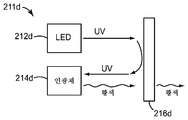
도 2d는 인광체 층이 특정 비-백색 색상, 예컨대 황색의 광을 방출하는 것을 제외하고는, 도 2c의 것과 유사한 원격 인광체 LED(211d)를 도시한다. 따라서, 원격 인광체 LED(211d)는 대부분 또는 전부가 이색성 반사기(216d)에 의해 인광체 층(214d) 상으로 반사되고 바람직하게는 인광체 층 상에 이미지화되는 UV 여기 광을 방출하는 펌프 LED(212d)를 포함한다. 인광체 층은 특정 비-백색 색상, 예컨대 황색의 인광체 광을 방출한다. 황색 색상은 단지 예시적이며, 다른 색상의 인광체 광이 또한 사용될 수 있다. 황색 인광체 광은 이색성 반사기(216d)에 의해 실질적으로 투과된다. 이 실시 형태에서, 이색성 반사기는 펌프 LED(212d)로부터의 여기 광에 대해 투과율을 거의 또는 전혀 갖지 않는 것으로 가정된다. 따라서, UV 여기 광이 이색성 반사기(216d)를 통해 거의 또는 전혀 투과되지 않는다. 황색 인광체 광은 단독으로 원격 인광체 LED(211d)의 광 출력을 제공한다. 황색 인광체 광이 상이한 색상의 인광체 광으로 대체되면, 원격 인광체 LED(211d)의 출력은 그러한 상이한 색상의 출력을 가질 것이다.Figure 2D shows a
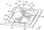
도 3은 추가의 세부 사항을 위에서 인용된 PCT 특허출원 공개 WO 2012/091973호에서 찾아볼 수 있는 원격 인광체 LED(311)의 개략 사시도이다. 원격 인광체 LED(311)는 여기에서 서브시스템(311)으로 지칭되고, 직교 x-y-z 좌표계와 관련하여 도시되어 있다. 서브시스템(311)은 외측 표면(329a) 및 기준점(329b)을 갖는 인광체 층(329)을 지지하는 기재(312)를 포함한다. 18개의 LED들이 인광체 층의 상부에 또는 달리 근접하게 배치되고, LED들은 6개의 이웃하는 LED들의 3개의 웨지-형상의(wedge-shaped) 그룹(330, 332, 334)들로 배열되며, 이웃하는 LED들의 각각의 그룹은 기재의 웨지-형상의 구역 내에 배치된다. LED들의 3개의 웨지-형상의 그룹들의 레이아웃, 및 각각의 그룹에서의 도시된 LED들의 개수 및 배향은 많은 가능한 배열들 중 하나이며, 제한적인 방식으로 해석되어서는 안된다. 예를 들어, 웨지-유사 형상 이외의 형상들이 또한 고려된다. LED는 바람직하게는 투명 중합체 또는 유리, 또는 다른 적합한 광-투과성 재료 내에 봉지되고, 봉지재의 외측 표면은 이색성 반사기(316)가 그러한 표면에 적용될 수 있고 그러한 표면에 형상적으로 정합할 수 있도록 오목하고 만곡될 수 있다. 이색성 반사기는 본 명세서에 기술된 다른 이색성 반사기와 동일하거나 유사할 수 있다. 이색성 반사기(316)의 형상은 정점(316a) 및 대칭 축 또는 광축(316b)을 한정할 수 있다. 광축(316b)은 서브시스템(311)의 광축과 일치할 수 있고, 기준점(329b) 및 정점(316a)을 통과할 수 있다.Figure 3 is a schematic perspective view of a
이웃하는 LED들의 그룹들은 인광체 층(329)의 차단되지 않은 웨지-형상의 부분(340, 342, 344)들에 의해 서로로부터 분리된다. 이와 관련하여 "차단되지 않은"은 LED가 실질적으로 존재하지 않는, 인광체 층(329)의 부분을 지칭한다. 또한, 이웃하는 LED들의 각각의 그룹은 점(329b)의 관점으로부터 인광체 층의 차단되지 않은 웨지-형상의 부분들 중 대체로 반대편의 부분인 기재의 웨지-형상의 구역에 놓인다. 기재의 웨지-형상의 구역(예컨대, LED의 웨지-형상의 그룹(330)이 놓인 영역) 및 인광체 층의 대응하는 웨지-형상의 부분(예컨대, 부분(340))의 각각의 쌍은 또한 점(329b)에 대하여 대체로 대칭일 수 있다. 광축(316b)이 점(329b)을 통과하도록 이색성 반사기(316)를 구성함으로써 그리고 이색성 반사기의 적합한 곡률 반경을 선택함으로써, 이색성 반사기에 의해 반사되는 이웃하는 LED들의 각각의 웨지-형상의 그룹으로부터의 LED 광의 일부분이 인광체 층의 대응하는 웨지-형상의 부분 상에 (적어도 대략적으로) 이미지화될 수 있다.The groups of neighboring LEDs are separated from each other by the uninterrupted wedge-shaped
3개의 LED 그룹들 각각 내의 이웃하는 LED들은 또한 점(329b)으로부터 그리고/또는 광축(316b)으로부터 (x-y 평면에 평행하게 측정된) 상이한 반경방향 거리로 배열되는 것으로 도시되어 있다. 도시된 배열에서, 예를 들어, 각각의 그룹 내의 하나의 LED는 축(316b)에 가장 가깝게 배치되고, 각각의 그룹 내의 3개의 LED는 축(316b)으로부터 가장 멀리 배치되며, 각각의 그룹 내의 2개의 LED는 축(316b)으로부터 중간 거리에 배치된다.Neighboring LEDs within each of the three LED groups are also shown to be arranged at different radial distances (measured parallel to the x-y plane) from
서브시스템(311)의 일 실시 형태에서, 모든 18개의 LED는 동일한 LED 방출 스펙트럼에 따라 LED 광을 방출할 수 있으며, 인광체 층(329)은 인광체 층의 조성 및 구조가 웨지-형상의 부분(340, 342, 344)들 전반에 걸쳐 그리고 이들 사이에서 동일하도록 균일한 조성 및 구조의 것일 수 있지만; 이색성 반사기의 특성은 상이한 색상들을 갖는 (상이한 LED들과 관련되는) 상이한 광대역 광 부분들을 제공하도록 맞춤될 수 있다. 특히, (이웃하는 LED들의 각각의 그룹 내의) 하나의 "근접" LED의 하위그룹과 관련된 제1 광대역 광 부분의 색상은 (이웃하는 LED들의 각각의 그룹 내의) 2개의 "중간" LED들의 하위그룹과 관련된 제2 광대역 광 부분의 색상과 상이할 수 있고, 이는 이어서 (이웃하는 LED들의 각각의 그룹 내의) 3개의 "먼" LED들의 하위그룹과 관련된 제3 광대역 광 부분의 색상과 상이할 수 있다. 이는 이색성 반사기가 하나의 근접한 LED의 하위그룹에 비해 2개의 중간 LED들의 하위그룹으로부터의 LED 광의 더 많은 부분을 투과시키고, 이색성 반사기가 또한 2개의 중간 LED들의 하위그룹에 비해 3개의 먼 LED들의 하위그룹으로부터의 LED 광의 더 많은 부분을 투과시키도록, 이색성 반사기의 평균 투과율 또는 반사 스펙트럼의 스펙트럼 대역 에지 또는 천이 구역이 적어도 일부 입사각에서 적어도 2개의 "중간" LED들의 하위그룹과 3개의 "먼" LED들의 하위그룹의 스펙트럼 방출과 중첩하는 것을 보장함으로써 달성될 수 있다. 광축(316b)으로부터의 증가하는 반경방향 거리에 따른 투과된 단파장 LED 광의 상대적 증가는 상이한 광대역 광 부분들의 상이한 색상들을 제공할 수 있다. 또한, 광원(310)으로부터의 전체 광대역 광 방출의 색상은 하나의 근접한 LED의 하위그룹, 2개의 중간 LED들의 하위그룹 및 3개의 먼 LED들의 하위그룹에 동력 공급되는 상대적 정도를 제어함으로써 제어되거나 조절될 수 있다.In one embodiment of the
서브시스템(311)의 다른 실시 형태에서, 상이한 LED와 관련된 인광체 층의 부분들에 대해 상이한 조성들 및/또는 구조들을 사용함으로써, 상이한 광대역 광 부분들에 대해 상이한 색상들이 달성될 수 있다. 예를 들어, LED 그룹(330)의 6개의 LED들에 의해 여기되는 인광체 층(329)의 웨지-형상의 부분(340)은 부분(342 및/또는 344)의 것과 상이한 조성 및/또는 구조를 가질 수 있다. 이때, 서브시스템으로부터의 전체 광대역 광 방출의 색상은 이웃하는 LED들의 하나의 그룹(예컨대, LED 그룹(330))이 이웃하는 LED들의 다른 그룹(예컨대, LED 그룹(332, 334))에 비해 동력 공급되는 상대적 정도를 제어 또는 조절함으로써 제어되거나 조절될 수 있다. 부가적으로 또는 대안적으로, 웨지-형상의 부분(340, 342, 344)들 중 하나, 일부 또는 전부는 광축(316b) 또는 기준점(329b)으로부터 상이한 반경방향 거리들에서 상이한 조성 및/또는 구조를 가질 수 있다. 만곡된 이색성 반사기(316)의 이미지화 특성으로 인해, 이웃하는 LED들의 각각의 그룹 내의 하나의 근접한 LED의 하위그룹은 기준점(329b)에 가장 근접한 웨지-형상의 인광체 부분의 부분을 우선적으로 여기시키는 경향이 있고, 이웃하는 LED들의 각각의 그룹 내의 2개의 중간 LED들의 하위그룹은 웨지-형상의 인광체 부분의 중간 부분을 우선적으로 여기시키는 경향이 있으며, 이웃하는 LED들의 각각의 그룹 내의 3개의 먼 LED들의 하위그룹은 기준점(329b)에서 가장 먼 웨지-형상 인광체 부분의 부분을 우선적으로 여기시키는 경향이 있다. 따라서, 반경방향으로 변하는 인광체 층이 하나의 근접한 LED의 하위그룹, 2개의 중간 LED들의 하위그룹 및 3개의 먼 LED들의 하위그룹에 동력 공급되는 상대적 정도를 조절 또는 제어함으로써 광원(310)으로부터의 전체 광대역 광 방출의 색상을 제어 또는 조절하도록 사용될 수 있다. 부가적으로 또는 대안으로, 웨지-형상의 부분(340, 342, 344)들 중 하나, 일부 또는 전부는 전술된 바와 같은, 상이한 방출 대역들의 둘 이상의 인광체들을 포함하는 패턴화된 인광체를 포함할 수 있다.In another embodiment of the
서브시스템(311)의 다른 실시 형태에서, 상이한 방출 스펙트럼들을 갖는 개별 LED들을 선택한 후 상이한 방출 특성들의 LED들이 동력 공급되는 상대적 정도를 제어하거나 조절함으로써, 상이한 광대역 광 부분들에 대해 상이한 색상들이 달성될 수 있다.In another embodiment of the
도 4는 추가의 세부 사항을 위에 인용된 PCT 특허출원 공개 WO 2012/091973호에서 찾아볼 수 있는 원격 인광체 LED(411)의 개략 사시도이다. 원격 인광체 LED(411)는 여기에서 서브시스템(411)으로 지칭되고, 직교 x-y-z 좌표계와 관련하여 도시되어 있다. 서브시스템(411)은 기재(418) 상에 배치되는 청색-광 방출 LED(412)를 포함하고, 기재는 또한 LED로부터의 청색 광에 노출될 때 보다 긴 파장의 가시 광을 방출하는 인광체 층(414)을 상부에서 구비한다. LED(412)는 와이어 본드(420)에 의해 전도성 트레이스에 연결될 수 있다.4 is a schematic perspective view of a
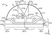
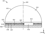
서브시스템(411)은 또한 LED와 인광체 층(414)을 향해 개방되고 이들을 둘러싸는 볼록 형상을 갖는 이색성 반사기(416)를 포함한다. 반사기(416)에 대한 곡률 중심이 점(419)으로 표시되어 있다. LED(412)는 점(419)에 비교적 근접하게 위치되며, 인광체 층(414)도 그러하다. 인광체 층(414)은 LED에 비해 약간 과대 크기로 도시되어 있다.
LED(412)에 의해 방출된 청색 광(413a)은 이색성 반사기(416)에 의해 부분적으로 반사되어 반사된 LED 광(413b)을 생성하고, 부분적으로 투과되어 투과된 LED 광(413c)을 생성한다. 반사된 LED 광(413b)은 인광체 층(414) 상으로 지향되며, 이는 인광체를 여기시키고, 인광체 층이 보다 긴 파장의 광(415a)을 방출하게 한다. 이러한 보다 긴 파장의 광은 이색성 반사기(416)에 의해 고도로 투과되어 인광체 광(415b)을 생성한다. 투과된 광(413c) 및 투과된 광(415b)은 공간적으로 조합되어 서브시스템 광원(411)의 광대역 출력 광, 예를 들어 백색 광을 제공한다. 내부 공간(417)은 LED와 인광체를 봉지하는 적합한 광-투과성 유리 또는 중합체 재료를 포함할 수 있고, 이색성 반사기는 그러한 봉지재의 외측 표면에 적용될 수 있다. 대안적으로, 내부 공간(417)은 충전되지 않을 수 있다.The
서브시스템(411)에서, 기재(418)는 바람직하게는 가요성, 하부의 히트 싱크(도시되지 않음)로의 보다 큰 열 전도(그리고 보다 낮은 열 저항)를 위해 그리고 공간 절약을 위해 얇다. 대체로 얇지만, 기재(418)는 바람직하게는 인접한 또는 이웃하는 구역(421b)에 비해 공동 구역(421a)에서 훨씬 더 얇도록 성형되거나 에칭되거나 달리 형상화되며, 이들 구역은 비스듬한 천이 구역에 의해 분리되는 것으로 도시되어 있다. 이웃하는 구역에 비해 공동 구역에서 훨씬 더 큰 열 전도도를 제공하는 감소된 두께는 바람직하게는 기재의 일부를 형성하는 유전체 층(418a)의 감소된 두께와 관련된다. 도면에서, 유전체 층(418a)은 이웃하는 구역(421b)들에서 두께 T1을 그리고 공동 구역(421a)에서 보다 작은 두께 T2를 갖는 것으로 도시되어 있다. LED에 전력을 제공하기 위해 원하는 대로 패턴화될 수 있는 전기 전도성 층(418b)이 유전체 층(418a) 위에 배치된다. 열 전도성 층(418c)이 층(418b)과 비교하여 유전체 층의 반대편의 주 표면 상에 배치된다. 일부 경우에는, 층(418b, 418c)들은 동일한 재료, 예컨대 구리로 구성될 수 있는 한편, 다른 경우에는 상이한 재료들이 사용될 수 있다. 따라서, 전기 전도성 층(418b)은 또한 열 전도성일 수 있고, 열 전도성 층(418c)은 또한 전기 전도성일 수 있다. 열 전도성 층(418c)은 바람직하게는 예컨대 적합한 열 계면 재료를 사용하여 적합한 히트 싱크에 접합된다.In
기재(418)의 박화된 구역은 바람직하게는 많은 경우에 기재의 핵심 구조적 구성요소인 유전체 층(418a)의 대응하는 박화된 구역과 관련된다. 적합한 유전체 층은 폴리에스테르, 폴리카르보네이트, 액정 중합체 및 폴리이미드를 포함한다. 적합한 폴리이미드는 듀폰(DuPont)으로부터 입수가능한 캡톤(KAPTON); 카네카 텍사스 코포레이션(Kaneka Texas corporation)로부터 입수가능한 아피칼(APICAL); 에스케이씨 코오롱 피아이 인크.(SKC Kolon PI Inc.)로부터 입수가능한 에스케이씨 코오롱 피아이(SKC Kolon PI); 및 우베 인더스트리즈(Ube Industries)로부터 입수가능한 우피렉스(UPILEX) 및 우피셀(UPISEL)이라는 상표명으로 입수가능한 것을 포함한다. 모두 일본 소재의 우베 인더스트리즈로부터 입수가능한, 우피렉스 에스(UPILEX S), 우피렉스 에스엔(UPILEX SN) 및 우피셀 브이티(UPISEL VT)라는 상표명으로 입수가능한 폴리이미드가 많은 응용에서 특히 유리하다. 이들 폴리이미드는 단량체, 예를 들어 바이페닐 테트라카르복실릭 다이언하이드라이드(BPDA) 및 페닐 다이아민(PDA)으로부터 제조된다.The thinned areas of the
유전체 층(418a)은 화학적 에칭, 플라즈마 에칭, 집속 이온-빔 에칭, 레이저 융제(laser ablation), 및 펀칭과 같은 임의의 적합한 방법을 사용하여 공동 구역에서 박화될 수 있다. 에칭에 관하여, 임의의 적합한 에칭제가 사용될 수 있고, 바람직한 에칭제는 유전체 층에 사용된 재료(들)에 의존할 수 있다. 적합한 에칭제는 알칼리 금속 염, 예컨대 수산화칼륨; 가용화제, 예컨대 아민 및 알코올, 예컨대 에틸렌 글리콜 중 하나 또는 둘 모두를 가진 알칼리 금속 염을 포함할 수 있다. 적합한 화학 에칭제는 본 명세서에 참고로 포함된 미국 특허출원 공개 제2007/0120089호(마오(Mao) 등)에 더 상세히 기재된 것과 같은 KOH/에탄올 아민/에틸렌 글리콜 에칭제를 포함할 수 있다. 다른 적합한 화학 에칭제는 본 명세서에 참고로 포함된, 통상적으로 양도된 PCT 특허출원 공개 WO 2012/061010호에 더 상세히 기재된 것과 같은 KOH/글리신 에칭제를 포함할 수 있다. 에칭 후, 유전체 층은 알칼리 KOH/과망간산칼륨(PPM) 용액, 예컨대 약 0.7 내지 약 1.0 중량% KOH 및 약 3 중량% KMnO4의 용액으로 처리될 수 있다. 유전체 층은 일면 또는 양면에서 전도성 층, 예컨대 도 4의 층(418b, 418c)으로 클래딩(cladding)될 수 있다. 전도성 층은 임의의 적합한 전기 및/또는 열 전도성 재료로 구성될 수 있지만, 전형적으로 구리를 포함한다. 전도성 층(들)이 회로로 형성된다면, 이것들은 원한다면 사전-패턴화될 수 있다. 일부 경우에, 가요성 기재는 유전체 재료 및 전도성 재료의 다수의 층들을 적층된 배열로 포함하는 다층 구성을 가질 수 있다.The
사용된 박화 절차의 유형은 공동 구역과 이웃하는 구역 사이의 천이와, 천이 구역에서 유전체 층과 다른 층의 측벽들의 특성에 영향을 미칠 수 있다. 화학 에칭은 비교적 얕은 측벽, 예컨대 가요성 기재의 평면으로부터 측정시 약 5 내지 60도, 또는 약 25 내지 28도의 범위 내의 전형적인 측벽 각도를 생성하기 위해 사용될 수 있다. 펀칭, 플라즈마 에칭, 집속 이온-빔 에칭 및 레이저 융제와 같은 다른 기술은 훨씬 더 가파른 측벽, 예컨대 최대 약 90도의 벽 각도를 생성할 수 있다. 펀칭에 의한 것과 같은 일부 경우에, 구멍이 완전히 유전체 층을 통해 형성될 수 있으며, 이는 아래에서 추가로 논의된다. 그러한 경우에, 전도성 층(418b 및/또는 418c)과 같은, 가요성 기재의 다른 층은 공동 구역 내의 LED(들) 및/또는 인광체 층에 대한 물리적 지지를 제공하기 위해 사용될 수 있다.The type of thinning procedure used can affect the transition between the cavity region and the neighboring regions and the properties of the dielectric layers and the sidewalls of the other layers in the transition region. The chemical etching may be used to create a typical sidewall angle within a range of about 5 to 60 degrees, or about 25 to 28 degrees, as measured from a relatively shallow side wall, such as the plane of the flexible substrate. Other techniques, such as punching, plasma etching, focused ion-beam etching and laser fluxing, can produce much steeper sidewalls, such as a wall angle of up to about 90 degrees. In some cases, such as by punching, the holes may be formed entirely through the dielectric layer, which is discussed further below. In such cases, other layers of the flexible substrate, such as
예시적인 실시 형태에서, 유전체 층은 LED(들) 및/또는 인광체 층으로부터의 열 전도를 증가시키기 위해 그리고 이들 구성요소를 보다 저온의 작동 온도로 유지시키기 위해 이웃하는 구역(421b)에 비해 공동 구역(421a)에서 상당히 더 얇다. 예를 들어, 두께 T2는 T1의 약 5 내지 25%일 수 있다. 또한, T2는 0 초과 10 마이크로미터 이하일 수 있는 반편, T1은 20 마이크로미터 이상일 수 있다. 예시적인 실시 형태에서, T1은 200 마이크로미터 이하일 수 있다. 열 전도를 증가시키는 것에 더하여, 공동 구역의 박화된 특성은 향상된 효율을 제공하기 위해 반사 재료로 코팅될 수 있는 경사진 측벽의 형성과 같은 다른 이점을 제공할 수 있다. 또한, LED(들) 및/또는 인광체 층을 박화된 공동 구역에서 기재에 부착함으로써, 이들 구성요소는 가요성 기재의 평면 위로 높이 연장되지 않아, 낮은 폼 팩터(form factor) 응용에 더 적합한 보다 낮은 프로파일의 장치를 생성한다.In an exemplary embodiment, the dielectric layer may have a higher thermal conductivity than the neighboring
독자는 도 3과 도 4의 원격 인광체 LED 및 본 명세서의 다른 부분에 기술된 것이 예시적이라는 것과, 다른 설계와 특성의 원격 인광체 LED가 또한 개시된 광대역 광원에 사용될 수 있다는 것을 상기하게 된다.The reader is reminded that the remote phosphor LEDs of FIGS. 3 and 4 and those described elsewhere herein are exemplary and remote phosphor LEDs of other designs and characteristics can also be used in the disclosed broadband light source.
하나의 그러한 광대역 광원(510)이 도 5에 개략적으로 도시되어 있다. 이러한 광원(510)은 수 개의 원격 인광체 LED(511a, 511b, 511c, 511d)들 및 수 개의 직접 방출 LED(530a, 530b)들을 조합한다. 이들 구성요소의 일부 또는 전부가 지지 기부(502)에 직접적으로 또는 하나 이상의 중간 층 또는 요소를 통해 간접적으로 부착될 수 있다. 광-투과성 벌브 또는 다른 커버 부재(540)가 원격 인광체 LED 및 직접 방출 LED를 밀봉하거나 달리 둘러싸기 위해 기부(502)에 직접적으로 또는 간접적으로 부착될 수 있다.One such
원격 인광체 LED(511a, 511b, 511c, 511d)들 각각은 도 1의 원격 인광체 LED(111) 또는 본 명세서에 개시된 다른 원격 인광체 LED와 동일하거나 유사할 수 있다. 간결성을 위해, 도 5의 각각의 원격 인광체 LED는 정확히 하나의 펌프 LED(요소(512a, 512b, 512c, 512d) 참조) 및 정확히 하나의 인광체 층(요소(514a, 514b, 514c, 514d) 참조)뿐만 아니라, 오목한 이색성 반사기(요소(516a, 516b, 516c, 516d) 참조)를 구비하는 것으로 도시되어 있다. 그러나, 더 많은 펌프 LED들, 및/또는 더 많고/많거나 상이하게 구성된 인광체 층들이 또한 도 5에 도시된 원격 인광체 LED들 중 하나, 일부 또는 전부에 사용될 수 있다. 4개의 원격 인광체 LED들이 도면에 도시되어 있지만, 단지 1개, 또는 2개, 또는 3개, 또는 4개 초과를 포함한 다른 개수의 원격 인광체 LED들이 사용될 수 있다. 1개 초과의 원격 인광체 LED들이 사용될 때, 이들은 서로 동일하거나 유사하도록 설계될 수 있거나, 이들은 상이한 출력 광을 개별적으로 제공하도록 상이한 설계, 예를 들어 상이한 개수의 펌프 LED, 및/또는 상이한 LED 유형(예컨대, 색상 또는 파장), 및/또는 상이한 개수의 인광체 층, 및/또는 상이한 인광체 층 두께, 및/또는 상이한 인광체 유형, 및/또는 상이한 이색성 반사기를 가질 수 있다. 원격 인광체 LED들은 광원(510)의 중심점 또는 광축에 대해 대칭으로 배열될 수 있거나, 이들은 비대칭으로 그리고/또는 불규칙하게 배열될 수 있다.Each of the
직접 방출 LED(530a, 530b)들 각각은 도 1의 직접 방출 인광체 LED(130) 또는 본 명세서에 개시된 다른 직접 방출 LED와 동일하거나 유사할 수 있다. 2개의 직접 방출 LED들이 도면에 도시되어 있지만, 단지 1개, 또는 3개, 또는 4개, 또는 4개 초과를 포함한 다른 개수의 직접 방출 LED들이 사용될 수 있다. 1개 초과의 직접 방출 LED들이 사용될 때, 이들은 서로 동일하거나 유사하도록 설계될 수 있거나, 이들은 상이한 출력 광을 개별적으로 제공하도록 상이한 설계, 예를 들어 상이한 스펙트럼 분포(예컨대 반치폭(full width at half maximum, FWHM)에 의해 측정되는 바와 같은 상이한 스펙트럼 폭을 포함함), 및/또는 상이한 피크 파장 또는 색상, 및/또는 상이한 출력 파워를 가질 수 있다. 직접 방출 LED들은 광원(510)의 중심점 또는 광축에 대해 대칭으로 배열될 수 있거나, 이들은 비대칭으로 그리고/또는 불규칙하게 배열될 수 있다.Each of the direct emitting
커버 부재(540)는 도 1의 커버 부재(140) 또는 본 명세서에 개시된 다른 커버 부재와 동일하거나 유사할 수 있다.The
기부(502)는 본 명세서에 개시된 다른 기부와 동일하거나 유사할 수 있다. 예를 들어, 기부(502)는 종래의 조명 기구에 적합할 수 있고, 입력 전력을 LED에 적합한 전압 및 전류로 변환시키기 위한 적합한 회로 및 요구되는 대로의 전기 접촉부를 구비할 수 있다. 바람직하게는, 기부(502)는 직접 방출 LED와 원격 인광체 LED가 상부에 장착되는 반사 표면(502a)을 포함한다. 적합한 반사기는 알루미늄, 은 또는 다른 적합한 금속, 및/또는 다층 유기 또는 무기 박막 적층물과 같은 반사율을 향상시키기 위한 유전체 재료의 층 또는 코팅; 및/또는 이산화티타늄-충전된 수지 층과 같은 착색된 층을 포함한다. 기부(502)는 또한 바람직하게는 광원(510)의 작동 동안에 다양한 LED와 인광체 층이 과도하게 고온으로 되지 않도록 양호한 열 전도도 및 히트 싱크 특성을 갖는다. 과도한 열은 그러한 구성요소의 효율과 수명을 감소시킬 수 있다. 광원(510)은 또한 광원(510) 내의 다양한 LED들에 동력 공급하는 제어 시스템(도 1)을 포함하거나 이 제어 시스템에 결합될 수 있다.The base 502 may be the same as or similar to the other bases disclosed herein. For example,
광원(510)에서, 다양한 원격 인광체 LED들로부터의 광과 다양한 직접 방출 LED들로부터의 광이 예를 들어 도 1과 관련하여 논의된 바와 같이 커버 부재(540)에 의해 투과되고 조합되어 광원의 광대역 출력 광을 제공한다. 하나의 예시적인 실시 형태에서, LED(530a)는 예컨대 600 내지 650 nm의 범위 내의 피크 파장을 갖는 적색 광을 방출할 수 있고, LED(530b)는 예컨대 445 내지 500 nm의 범위 내의 피크 파장을 갖는 청색 광을 방출할 수 있으며, 4개의 원격 인광체 LED들 각각은 청색 또는 UV 펌프 LED를 사용하고 황색 인광체 광을 방출할 수 있으며, 광원(510)의 출력 광은 실질적으로 백색일 수 있다. 다른 실시 형태에서, 공칭적으로 동일한 색상(예컨대, 청색 또는 적색)의 그러나 상이한 피크 파장을 갖는 다수의 직접 방출 LED들이 광원의 광대역 광 출력의 연색 평가 지수(CRI) 및/또는 색상 품질 스케일(color quality scale, CQS)과 발광 효율을 증가시키기 위해 사용될 수 있다. 예를 들어, 각각 청색 광을 방출하지만 상이한 피크 파장을 갖는 2개의 직접 방출 LED들, 및/또는 각각 적색 광을 방출하지만 상이한 피크 파장을 갖는 2개의 직접 방출 LED들이 사용될 수 있다. 피크 파장의 차이는 예를 들어 5 또는 10 nm 이상, 그러나 50 또는 40 nm 미만일 수 있다. 예를 들어, 하나의 직접 방출 청색 LED가 445 nm의 피크 파장을 가질 수 있고, 다른 직접 방출 청색 LED가 480 nm의 피크 파장을 가질 수 있다.In
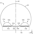
다른 광대역 광원(610)이 도 6에 측면도 또는 단면도로 대략적으로 도시되어 있다. 이러한 광원(610)은 수 개의 원격 인광체 LED(611a, 611b)들 및 수 개의 직접 방출 LED(630a, 630b)들을 조합한다. 이들 구성요소의 일부 또는 전부가 지지 기부(602)에 직접적으로 또는 하나 이상의 중간 층 또는 요소를 통해 간접적으로 부착될 수 있다. 광-투과성 벌브 또는 다른 커버 부재(640)가 원격 인광체 LED 및 직접 방출 LED를 밀봉하거나 달리 둘러싸기 위해 기부(602)에 직접적으로 또는 간접적으로 부착될 수 있다. 광원(610)은 대칭축 또는 광축(604)을 갖는 것으로 도시되어 있다.Another
원격 인광체 LED(611a, 611b)는 도 6a에 더 상세히 도시된 인광체 층 배열을 제외하고는 도 5의 원격 인광체 LED와 유사할 수 있다. 도 6의 각각의 원격 인광체 LED는 정확히 하나의 펌프 LED(요소(612a, 612b) 참조) 및 특정 인광체 층 배열(요소(614a, 614b) 참조)뿐만 아니라 오목한 이색성 반사기(요소(616a, 616b) 참조)를 구비하는 것으로 도시되어 있다. 그러나, 더 많은 펌프 LED들 및/또는 더 많고/많거나 상이하게 구성된 인광체 층들이 또한 도 6에 도시된 원격 인광체 LED들 중 하나 또는 둘 모두에 사용될 수 있다. 2개의 원격 인광체 LED가 도 6의 측면도에 도시되어 있지만, 광원(610)은 예를 들어 도 5에 배치된 바와 같은 총 4개의 원격 인광체 LED를 구비할 수 있거나, 광원(610)은 단지 1개, 또는 3개, 또는 5개, 또는 그 초과와 같은 다른 개수의 원격 인광체 LED들을 구비하도록 변경될 수 있다. 원격 인광체 LED(611a, 611b)들은 광원(610)의 대칭축 또는 광축(641)에 대해 대칭으로 위치되는 것으로 도 6의 측면도에 도시되어 있다. 다른 실시 형태에서, 원격 인광체 LED들은 대칭으로 위치될 필요는 없다. 하나 초과의 원격 인광체 LED들이 사용될 때, 이들은 위에서 논의된 바와 같이 서로 동일하거나 상이할 수 있다.
직접 방출 LED(630a, 630b)들은 도 5의 직접 방출 인광체 LED(530a, 530b)와 동일하거나 유사할 수 있다. 2개의 직접 방출 LED들이 도면에 도시되어 있지만, 단지 1개, 또는 3개, 또는 4개, 또는 4개 초과를 포함한 다른 개수의 직접 방출 LED들이 사용될 수 있다. 하나 초과의 직접 방출 LED들이 사용될 때, 이들은 위에서 논의된 바와 같이 동일하거나 상이할 수 있다. 도 6의 측면도에서, LED(630a, 630b)들은 광축(641)에 대해 대칭으로 위치되는 것으로 도시되어 있다. 다른 실시 형태에서, 직접 방출 LED들은 대칭으로 위치될 필요는 없다.The direct emitting
커버 부재(640)는 도 5의 커버 부재(540)와 동일하거나 유사할 수 있고, 기부(602)는 도 5의 기부(502)와 동일하거나 유사할 수 있다.The
광원(610)에서, 원격 인광체 LED(611a, 611b)들로부터의 광과 직접 방출 LED(630a, 630b)들로부터의 광이 예를 들어 도 5와 관련하여 논의된 바와 같이 커버 부재(640)에 의해 투과되고 조합되어 광원의 광대역 출력 광을 제공한다. 하나의 예시적인 실시 형태에서, LED(630a)는 예컨대 600 내지 650 nm의 범위 내의 피크 파장을 갖는 적색 광을 방출할 수 있고, LED(630b)는 예컨대 445 내지 500 nm의 범위 내의 피크 파장을 갖는 청색 광을 방출할 수 있으며, 2개의 원격 인광체 LED들 각각은 청색 또는 UV 펌프 LED를 사용하고 황색 인광체 광을 방출할 수 있으며, 광원(610)의 출력 광은 실질적으로 백색일 수 있다.In
도 6a는 도 6에 도시된 원격 인광체 LED(611a, 611b)들 중 하나 또는 둘 모두와 동일할 수 있는 원격 인광체 LED(611)의 개략 측면도 또는 단면도이다. 도 6a에서, 원격 인광체 LED(611)는 펌프 LED(612), 인광체 층(614) 및 이색성 반사기(616)를 구비한다. 이색성 반사기(616)는 평철(plano-convex) 렌즈 또는 몸체(619)의 외측 만곡 표면 전체를 덮지만, 다른 실시 형태에서, 이색성 반사기는 단지 외측 만곡 표면의 일부분만을 덮도록 형성될 수 있다. 반사기(616)는 LED(612)와 인광체 층(614)에 대해 오목하다. 이색성 반사기(616)는 또한 LED(612) 및 인광체 층(614) 둘 모두를 덮는다. 몸체(619)는 원격 인광체 LED(611)의 광축(621)을 한정하는 대칭축을 갖는다. 몸체(619)의 외측 만곡 표면은 곡률 중심이 점(620)에 배치되는 구의 섹션이다. 펌프 LED(612)는 y-방향을 따라 점(620)에 근접하게 위치되지만 그로부터 이격된다. 이러한 방식으로 위치되기 때문에 그리고 반사기(616)의 오목한 형상으로 인해, 반사기(616)는 LED(612)로부터의 여기 광을 점(620)의 반대편에 있는 인광체 층(614)의 부분 상으로, 즉 도 6a의 관점으로부터 점(620)의 좌측으로, 대략적으로 이미지화한다.6A is a schematic side view or cross-sectional view of a
인광체 층(614)은 상이한 인광체 재료들로 구성될 수 있는 2개의 보다 얇은 인광체 층(617, 618)들로 분할된다. 일반적으로, 인광체 층은 매우 다양한 구성을 가질 수 있고, 별개의 층들, 구역들, 또는 패턴화된 영역들에서 동일하거나 상이한 인광체 재료를 포함할 수 있다. 예시적인 실시 형태에서, 상부 인광체 층(618)은 적색 인광체 광을 방출하고, 하부 인광체 층(617)은 녹색 인광체 광을 방출한다. 예를 들어 광학 접착제의 층일 수 있는 투명한 광-투과성 층(615)이 인광체 층(614)(보다 구체적으로, 상부 인광체 층(618))을 몸체(619)의 평탄한 표면으로부터 분리시킨다. 펌프 LED(612)의 상부 방출 주 표면(613)이 도시된 바와 같이 층(615) 내에 배치될 수 있다.
기부(603)는 도 6의 기부(602)와 동일할 수 있거나, 기부(603)는 원격 인광체 LED(611)의 제조에 사용된 상이한 지지 기재일 수 있는데, 이러한 기부(603)는 이어서 도 6의 기부(602)에 접착, 접합 또는 달리 부착된다. 기부(603)는 바람직하게는 LED(612)로부터 그리고 인광체 층(614)으로부터 열을 추출하기 위해 양호한 열 전도도를 갖는다. 기부(603)는 펌프 LED의 전기적 제어를 허용하도록 펌프 LED에 연결되는 전기 접촉부 또는 트레이스(도시되지 않음)를 포함할 수 있다. 기부(603)는 또한 바람직하게는 인광체 층(614)과 펌프 LED(612)에 대면하는 반사 표면(601)을 구비하여, 원격 인광체 LED의 후방에 도달하는 그리고 흡수되거나 달리 손실될 인광체 광과 여기 광이 원격 인광체 LED의 전방을 향해 방향전환되어 원격 인광체 LED(611)의 효율과 광 출력을 증가시킬 수 있게 한다.
실시예Example
본 명세서에 개시된 하이브리드 광대역 광원들 중 일부를 모델링하거나 시뮬레이션하였으며, 이들의 출력 특성을 평가하였다. 시뮬레이션은 라이트툴즈(LightTools)™ 광학 설계 소프트웨어를 사용하였다. 실시예들 각각은 도 5 및 도 6에 전반적으로 도시된 바와 같이 기부 상에 배열된 그리고 벌브 또는 커버 부재를 갖는 4개의 원격 인광체 LED와 2개의 직접 방출 LED를 사용하였지만, 여기서 원격 인광체 LED는 도 6과 도 6a에 도시된 구성의 것이었다.Some of the hybrid broadband light sources disclosed herein have been modeled or simulated and their output characteristics evaluated. The simulation used LightTools ™ optical design software. Each of the embodiments used four remote phosphor LEDs and two direct emitting LEDs arranged on the base and having a bulb or cover member as shown generally in Figures 5 and 6, 6 and Fig. 6A.
시뮬레이션은 다음과 같이 각각의 실시예에 구현된 최적화 루틴을 사용하였다: 일부 특정 출력 파라미터들에 목표 값과 상대 가중치를 할당함으로써 메리트 함수(merit function)를 설정하였고, 수 개의 설계 파라미터들을 최적화 목적을 위해 독립 변수로서 처리하였고 설계 파라미터들에 상한과 하한을 할당하였다. 소프트웨어는 이어서 특정 출력 파라미터들에 의해 정의된 메리트 함수를 최대화시키는 독립 변수 설계 파라미터들 각각에 대한 최적화된 값을 (이들 각자의 상한 및 하한 내에서) 계산하였다.The simulation used the optimization routines implemented in each of the embodiments as follows: By setting a merit function by assigning target values and relative weights to some specific output parameters, and by designing several design parameters for optimization purposes And the upper and lower limits were assigned to the design parameters. The software then computed the optimized values (within their respective upper and lower limits) for each of the independent parameter design parameters that maximized the merit function defined by the specific output parameters.
최대 관심대상의 출력 파라미터는 광원에 의해 방출된 광대역 출력 광의, CIE x 및 y 색상 좌표에 관하여 측정된 색상이었다. 이들 CIE x 및 y 색상 좌표의 목적을 위해, 광원의 출력 광을 크기가 20 mm × 20 mm이며 오목한 커버 부재(도 5의 커버 부재(540), 도 6의 커버 부재(640))의 정점에 접하고 그에 중심을 둔 정사각형 검출 평면 내에서 공간적으로 평균하였다. 최적화에 실질적으로 영향을 미치지 않도록 출력 색상보다 작은 상대 가중치 계산 차수(relative weight order of magnitude)가 할당된 관심대상의 다른 출력 파라미터들은 와트 단위로 측정된 광원의 방사 출력(radiometric output); 루멘 단위로 측정된 광원의 광도 출력(photometric output); 광원 출력의 연색 평가 지수(CRI); 광원 출력의 평균(general) 색상 품질 스케일(CQS) - CQS는 백색 광원의 조명 품질의 척도로서 CRI에 대한 대안으로서 미국 국립 표준 기술 연구소(NIST)에 의해 개발된 알려진 스케일을 지칭함 -; 및 광원 출력의 상관 색상 온도(correlated color temperature, CCT)였다. 이들 출력 파라미터 모두를 규정된 검출 평면에서 검출된 광대역 광원으로부터의 모든 광에 대해 평가하였다.The output parameter of greatest interest was the measured color with respect to the CIE x and y color coordinates of the broadband output light emitted by the light source. For the purpose of these CIE x and y color coordinates, the output light of the light source is incident on the apex of a concave cover member (cover
각각의 시뮬레이션에서 6개의 독립 변수 설계 파라미터들, 즉 각각 0 내지 3 와트로 제한된, 2개의 직접 방출 LED들 각각의 방사 파워 출력; 하나의 (청색-방출) LED에 대해 450 내지 480 nm로 그리고 다른 하나의 (적색-방출) LED에 대해 550 내지 620 nm로 제한된, 각각의 직접 방출 LED의 피크 방사 파장(λ); 및 각각 0.0001 내지 100,000,000개 입자/㎣로 제한된, 2개의 인광체 층(도 6a의 층(617, 618) 참조)에 대한 인광체 입자 밀도를 사용하였다.The emission power output of each of the two direct emission LEDs, each limited to six independent parameter design parameters, 0 to 3 watts each; The peak emission wavelength (?) Of each direct emitting LED, limited to 450 to 480 nm for one (blue-emitting) LED and 550 to 620 nm for the other (red-emitting) LED; And the phosphor particle densities for the two phosphor layers (see
시뮬레이션된 실시 형태들에 대한 추가의 설계 특징들은 하기를 포함하였다:Additional design features for the simulated embodiments include:
![]()
![]()
![]()
![]()
![]()
![]()
![]()
![]()
![]()
![]()
![]()
![]()
![]()
![]()
![]()
![]()
![]()
![]()
실시예 1Example 1
제1 실시예에서, 펌프 LED(612)는 445 nm의 피크 파장을 가졌고, 광원(도 5의 510과 도 6의 610 참조)의 목표 출력 색상이 각각 (x, y) CIE 색상 좌표에 대해 (0.44, 0.40)으로 설정되었다. 다른 출력 파라미터에 대한 목표 값들 및 메리트 함수에서의 이들 각자의 가중치가 하기 표 1에 제공되어 있다.In the first embodiment, the
이어서 광학 설계 소프트웨어를 실행하였다. 시뮬레이션의 일부로서, 출력 파라미터에 대한 최적화된 값을 계산하였다. 이들 계산의 결과가 표 1에 포함되어 있다. 6개의 독립 변수 설계 파라미터에 대한 최적화된 값을 또한 계산하였다. 이들 계산의 결과가 하기 표 2에 나타나 있다. 이 표에서, "적색 LED"가 직접 방출 LED(530a(도 5) 또는 630a(도 6))를 지칭하고, "청색 LED"가 직접 방출 LED(530b(도 5) 또는 630b(도 6))를 지칭한다는 것에 주목한다. 규정된 검출기 평면 내에서의 스펙트럼 파워 출력을 각자의 파라미터들 모두에 대한 최적화된 값을 가정하여 또한 계산하였다. 실시예 1에 대한 이러한 스펙트럼 파워 출력이 도 9에 도시되어 있다.Optical design software was then implemented. As part of the simulation, an optimized value for the output parameter was calculated. The results of these calculations are included in Table 1. Optimized values for six independent parameter design parameters were also calculated. The results of these calculations are shown in Table 2 below. 6), and the "blue LED" refers to the direct emitting


실시예 2Example 2
이어서 제2 실시예를 광학 설계 소프트웨어를 사용하여 시뮬레이션하였다. 이러한 실시예 2는 목표 출력 색상이 각각 (x, y) CIE 색상 좌표에 대해 (0.35, 0.35)로 변화된 것을 제외하고는 실시예 1과 동일하였다. 다른 출력 파라미터에 대한 목표 값들 및 메리트 함수에서의 이들 각자의 가중치가 하기 표 3에 나타낸 바와 같이 동일하였다.The second embodiment was then simulated using optical design software. Example 2 was the same as Example 1 except that the target output hue was changed to (0.35, 0.35) for each (x, y) CIE hue coordinate. The target values for the other output parameters and their respective weights in the merit function were the same as shown in Table 3 below.
광학 설계 소프트웨어가 역시, 표 3에 포함된 출력 파라미터에 대한 최적화된 값을 계산하였다. 6개의 독립 변수 설계 파라미터에 대한 최적화된 값을 또한 계산하였고, 이들이 하기 표 4에 나타나 있다. 규정된 검출기 평면 내에서의 스펙트럼 파워 출력을 각자의 파라미터들 모두에 대한 최적화된 값을 가정하여 또한 계산하였다. 실시예 2에 대한 이러한 스펙트럼 파워 출력이 도 10에 도시되어 있다.The optical design software also computed optimized values for the output parameters included in Table 3. Optimized values for the six independent parameter design parameters were also calculated and are shown in Table 4 below. The spectral power output in the specified detector plane was also calculated assuming an optimized value for each of the parameters. This spectral power output for Example 2 is shown in FIG.


실시예 3Example 3
이어서 제3 실시예를 광학 설계 소프트웨어를 사용하여 시뮬레이션하였다. 이러한 실시예 3은 목표 출력 색상이 각각 (x, y) CIE 색상 좌표에 대해 (0.32, 0.28)로 변화된 것을 제외하고는 실시예 1 및 실시예 2와 동일하였다. 다른 출력 파라미터에 대한 목표 값들 및 메리트 함수에서의 이들 각자의 가중치가 하기 표 5에 나타낸 바와 같이 동일하였다.The third embodiment was then simulated using optical design software. This third embodiment was the same as Embodiments 1 and 2 except that the target output hue was changed to (0.32, 0.28) for each (x, y) CIE hue coordinate. The target values for the other output parameters and their respective weights in the merit function were the same as shown in Table 5 below.
광학 설계 소프트웨어가 역시, 표 5에 포함된 출력 파라미터에 대한 최적화된 값을 계산하였다. 6개의 독립 변수 설계 파라미터에 대한 최적화된 값을 또한 계산하였고, 이들이 하기 표 6에 나타나 있다. 규정된 검출기 평면 내에서의 스펙트럼 파워 출력을 각자의 파라미터들 모두에 대한 최적화된 값을 가정하여 또한 계산하였다. 실시예 3에 대한 이러한 스펙트럼 파워 출력이 도 11에 도시되어 있다.The optical design software also computed optimized values for the output parameters included in Table 5. Optimized values for the six independent parameter design parameters were also calculated and are shown in Table 6 below. The spectral power output in the specified detector plane was also calculated assuming an optimized value for each of the parameters. This spectral power output for Example 3 is shown in Fig.

실시예 4Example 4
이어서 제4 실시예를 광학 설계 소프트웨어를 사용하여 시뮬레이션하였다. 이러한 실시예 4는 펌프 LED(612)가 445 nm보다는 415 nm의 피크 파장을 갖는 것을 제외하고는 실시예 1과 동일하였다. 여기 파장의 이러한 변화로 인해, 적색 및 녹색 인광체 재료들의 양자 효율이 실시예 1에 대한 91%로부터 본 실시예 4에 대한 59%로 감소되었다. 다른 출력 파라미터에 대한 목표 값들 및 메리트 함수에서의 이들 각자의 가중치가 목표 방사 파워가 6 와트로부터 3 와트로 감소된 것을 제외하고는 하기 표 7에 나타낸 바와 같이 실시예 1의 것과 동일하였다.The fourth embodiment was then simulated using optical design software. Example 4 was the same as Example 1 except that the
광학 설계 소프트웨어가 역시, 표 7에 포함된 출력 파라미터에 대한 최적화된 값을 계산하였다. 6개의 독립 변수 설계 파라미터에 대한 최적화된 값을 또한 계산하였고, 이들이 하기 표 8에 나타나 있다. 규정된 검출기 평면 내에서의 스펙트럼 파워 출력을 각자의 파라미터들 모두에 대한 최적화된 값을 가정하여 또한 계산하였다. 실시예 4에 대한 이러한 스펙트럼 파워 출력이 도 12에 도시되어 있다.The optical design software also computed optimized values for the output parameters included in Table 7. Optimized values for the six independent parameter design parameters were also calculated and are shown in Table 8 below. The spectral power output in the specified detector plane was also calculated assuming an optimized value for each of the parameters. This spectral power output for Example 4 is shown in FIG.


참조 장치Reference device
비교 목적을 위해, 여기에서 "참조 장치"로 지칭되는 대안적인 광대역 광원을 또한 시뮬레이션하였다. 이들 광원은 하기의 변화를 제외하고는 실시예 1 내지 실시예 4와 구성이 유사하였다:For comparison purposes, an alternative broadband light source, also referred to herein as a "reference device" was also simulated. These light sources were similar in composition to Examples 1 to 4 except for the following changes:
![]()
![]()
![]()
![]()
이들 변화를 고려하여, 이전에 원격 인광체 LED(611)로서 알려진 각각의 서브시스템은 더 이상 원격 인광체 LED 자체가 아니었는데, 그 이유는 LED(612)로부터의 광이 더 이상 인광체 층(617, 618) 상으로 실질적으로 반사되어 인광체를 여기시키지 않았기 때문이다. 또한, 이전에 직접 방출 LED(530a-b, 630a-b)로서 알려진 LED는 더 이상 직접-방출형이 아니었는데, 그 이유는 이들 LED로부터의 광이 이제는 변형 커버 부재 내의 인광체 재료를 통해 전파되도록 요구되었기 때문이다.In light of these changes, each subsystem previously known as the
참조 장치 1Reference device 1
제1 참조 장치를 이전과 동일한 광학 설계 소프트웨어를 사용하여 시뮬레이션하였다. 이러한 참조 장치는 위에서 언급된 변화를 제외하고는 실시예 1과 동일하였다. LED(612)는 445 nm의 피크 파장을 가졌다. 제1 (외측) 변형 커버 부재는 층(618)에 사용된 동일한 적색-방출 인광체 재료로 구성되었고, 제2 (내측) 변형 커버 부재는 층(617)에 사용된 동일한 녹색-방출 인광체 재료로 구성되었다. 출력 파라미터에 대한 목표 값들 및 메리트 함수에서의 이들 각자의 가중치가 하기 표 9에 나타낸 바와 같이 실시예 1의 것과 동일하였다.The first reference device was simulated using the same optical design software as before. This reference device was the same as Example 1 except for the changes mentioned above. The
광학 설계 소프트웨어가 역시, 표 9에 포함된 출력 파라미터에 대한 최적화된 값을 계산하기 위해 사용되었다. 6개의 독립 변수 설계 파라미터에 대한 최적화된 값을 또한 계산하였고, 이들이 하기 표 10에 나타나 있다. 위의 실시예들에 사용된 동일한 검출기 평면 내에서의 스펙트럼 파워 출력을 각자의 파라미터들 모두에 대한 최적화된 값을 가정하여 또한 계산하였다. 참조 장치 1에 대한 이러한 스펙트럼 파워 출력이 도 13에 도시되어 있다.Optical design software was also used to calculate the optimized values for the output parameters included in Table 9. Optimized values for the six independent parameter design parameters were also calculated and are shown in Table 10 below. The spectral power output in the same detector plane used in the above embodiments was also calculated assuming an optimized value for each of the parameters. This spectral power output for reference device 1 is shown in Fig.


참조 장치 2Reference device 2
이어서 제2 참조 장치를 광학 설계 소프트웨어를 사용하여 시뮬레이션하였다. 이러한 참조 장치 2는 변형 커버 부재들에 사용된 인광체 재료들이 뒤바뀌었다는 것을 제외하고는 참조 장치 1과 동일하였다. 제1 (외측) 변형 커버 부재는 층(617)에 사용된 동일한 녹색-방출 인광체 재료로 구성되었고, 제2 (내측) 변형 커버 부재는 층(618)에 사용된 동일한 적색-방출 인광체 재료로 구성되었다. 출력 파라미터에 대한 목표 값들 및 메리트 함수에서의 이들 각자의 가중치가 하기 표 11에 나타낸 바와 같이 동일하였다.The second reference device was then simulated using optical design software. This reference device 2 was the same as the reference device 1 except that the phosphor materials used in the deformable cover members were reversed. The first (outer) deformable cover member was comprised of the same green-emitting phosphor material used in
광학 설계 소프트웨어가 역시, 표 11에 포함된 출력 파라미터에 대한 최적화된 값을 계산하였다. 6개의 독립 변수 설계 파라미터에 대한 최적화된 값을 또한 계산하였고, 이들이 하기 표 12에 나타나 있다. 규정된 검출기 평면 내에서의 스펙트럼 파워 출력을 각자의 파라미터들 모두에 대한 최적화된 값을 가정하여 또한 계산하였다. 참조 장치 2에 대한 이러한 스펙트럼 파워 출력이 도 14에 도시되어 있다.The optical design software also computed optimized values for the output parameters included in Table 11. Optimized values for the six independent parameter design parameters were also calculated and are shown in Table 12 below. The spectral power output in the specified detector plane was also calculated assuming an optimized value for each of the parameters. This spectral power output for reference device 2 is shown in Fig.


참조 장치 3Reference device 3
이어서 제3 참조 장치를 광학 설계 소프트웨어를 사용하여 시뮬레이션하였다. 이러한 참조 장치 3은 LED(612)가 445 nm보다는 415 nm의 피크 파장을 가졌다는 것을 제외하고는 참조 장치 2와 동일하였다. 출력 파라미터에 대한 목표 값들 및 메리트 함수에서의 이들 각자의 가중치가 하기 표 13에 나타낸 바와 같이 참조 장치 2의 것과 동일하였다.The third reference device was then simulated using optical design software. This reference device 3 was identical to reference device 2 except that the
광학 설계 소프트웨어가 역시, 표 13에 포함된 출력 파라미터에 대한 최적화된 값을 계산하였다. 6개의 독립 변수 설계 파라미터에 대한 최적화된 값을 또한 계산하였고, 이들이 하기 표 14에 나타나 있다. 규정된 검출기 평면 내에서의 스펙트럼 파워 출력을 각자의 파라미터들 모두에 대한 최적화된 값을 가정하여 또한 계산하였다. 참조 장치 3에 대한 이러한 스펙트럼 파워 출력이 도 15에 도시되어 있다.The optical design software also computed optimized values for the output parameters included in Table 13. Optimized values for the six independent parameter design parameters were also calculated and are shown in Table 14 below. The spectral power output in the specified detector plane was also calculated assuming an optimized value for each of the parameters. This spectral power output for reference device 3 is shown in Fig.


추가 논의Further discussion
참조 장치의 보다 큰 변형 커버 부재에 비해, 실시예에 사용된 원격 인광체 LED의 상대적으로 작은 크기로 인해, 실시예에 사용된 적색-방출 및 녹색-방출 인광체의 양은 참조 장치에 사용된 것보다 상당히 적다.Due to the relatively small size of the remote phosphor LED used in the embodiment, the amount of red-emitting and green-emitting phosphors used in the examples is significantly greater than that used in the reference device little.
사용된 인광체 재료의 양을 광이 입사하는 인광체의 주 표면의 면적에 관하여 정량화할 수 있다. 예를 들어, 도 6a의 실시 형태에서, 인광체 층(614)은 층(615)과 계면을 공유하며, 이러한 공유된 계면은 여기 광이 입사하는 인광체 층(614)의 주 표면(즉, 최대 표면적의 표면)과 일치한다. 간단함 또는 근사를 위해 LED(612)에 의해 차지되는 체적 또는 면적을 무시하고, 인광체 층(614)이 연속적이고 몸체(619)의 평탄한 표면과 동일한 공간에 있다고 가정하면, 인광체 층(614)의 입사 주 표면의 면적은 약 12.6 ㎟이다. 원격 인광체 LED들 중 4개가 광대역 광원 내에 포함되기 때문에, Aphosphor로서 지칭할 수 있는 총 또는 집합 인광체 표면적은 약 50 ㎟이다. 따라서, 여기 광이 입사하는 광원 내의 인광체 층의 집합 표면적, 또는 더 간단하게는 집합 인광체 표면적 또는 Aphosphor는 실시예 1 내지 실시예 4 각각에 대해 약 50 ㎟이다. 원한다면, 인광체의 이러한 양은 훨씬 더 상당히 감소될 수 있는데, 그 이유는 오목한 이색성 반사기의 집속 특성과 펌프 LED의 배치로 인해, 인광체 층이 광원의 출력 광의 감소 또는 변화가 거의 또는 전혀 없이 몸체(619)의 평탄 표면의 크기의 일부분만을 덮도록 패턴화될 수 있기 때문이다. 예를 들어, 집합 인광체 표면적(Aphosphor)은 출력 광의 감소 또는 변화가 거의 또는 전혀 없이 50으로부터 20 이상 또는 심지어 10 ㎟로 감소될 수 있다.The amount of the phosphor material used can be quantified with respect to the area of the main surface of the light incident on the phosphor. 6A, the
대조적으로, 참조 장치에 사용된 인광체의 양은 상당히 더 많다. 펌프 광이 입사하는 조합된 변형 커버 부재의 표면적은 적어도 대략 반경 10 mm의 반구의 표면적이거나 약 628 ㎟ 이상이다. 이는 몸체(619)의 기부에 있는 인광체 층의 훨씬 더 작은 표면적을 무시하며, 이러한 보다 작은 인광체 층은 출력 광의 감소 또는 변화가 거의 또는 전혀 없이 참조 장치로부터 생략될 수 있다.In contrast, the amount of phosphor used in the reference device is significantly higher. The surface area of the combined deformed cover member into which the pump light is incident is at least the surface area of a hemisphere having a radius of about 10 mm or at least about 628 mm < 2 >. This neglects a much smaller surface area of the phosphor layer at the base of the
일반성을 위해, 인광체의 양은 또한 집합 인광체 표면적을 광원 내의 모든 펌프 LED들의 집합 방출 표면적으로 나눈 것에 의하여 비로서 표현될 수 있다. 실시예 1 내지 실시예 4의 경우에, 각각 1 ㎟의 주 방출 표면적을 갖는 4개의 펌프 LED(612)를 사용하였다. 이때, ALED로 지칭할 수 있는 집합 펌프 LED 표면적은 4 ㎟이다. 실시예 1 내지 실시예 4 각각에서 Aphosphor 대 ALED의 비는 50/4 ![]()
![]()
![]()
![]()
![]()
![]()
대조적으로, 참조 장치에서 Aphosphor 대 ALED의 비는 628/6 ![]()
![]()
바람직하게는, 적어도 하나의 원격 인광체 LED와 적어도 하나의 직접 방출 LED를 이용하는 개시된 광대역 광원에 대한 비 Aphosphor/ALED는 50, 또는 20, 또는 15, 또는 10, 또는 5, 또는 2 이하이다.Preferably, the non-Aphosphor / ALED for the disclosed broadband light source using at least one remote phosphor LED and at least one direct emitting LED is 50, or 20, or 15, or 10, or 5, or 2 or less.
실시예 1, 참조 장치 1 및 참조 장치 2 각각은 x, y 색상 좌표에 대해 (0.44, 0.40)의 목표 출력 색상을 가졌고, 각각 또한 445 nm 피크 파장 LED들을 4개의 LED(612)로서 사용하였다. 이들 세 가지 실시 형태에 대한 다양한 최적화된 출력 파라미터와 전술된 바와 같은 집합 인광체 표면적(Aphosphor)이 표 15에서 비교되어 있다. 또한, 수광기에 의해 검출된 총 루멘 출력을 원격 인광체 및 직접 방출 LED에 의해 방출된 광의 총 방사 파워(와트 단위)로 나눈, "lm/Radiant W"로 지칭되는 비가 비교되어 있다.Example 1, reference device 1 and reference device 2 each had a target output hue of (0.44, 0.40) for x, y color coordinates, and each also used 445 nm peak wavelength LEDs as four

실시예 4 및 참조 장치 3 각각은 x, y 색상 좌표에 대해 (0.44, 0.40)의 목표 출력 색상을 가졌고, 각각 또한 415 nm 피크 파장 LED들을 4개의 LED(612)로서 사용하였다. 이들 세가지 실시 형태에 대한 다양한 최적화된 출력 파라미터가 표 16에서 비교되어 있다.Each of Example 4 and Reference Device 3 had a target output hue of (0.44, 0.40) for x, y color coordinates, and each also used 415 nm peak wavelength LEDs as four

표 15 및 표 16과 위의 시뮬레이션 결과는 적어도 하나의 인광체 LED와 적어도 하나의 직접 방출 LED를 사용하는 개시된 광대역 광원이 상당히 감소된 인광체 양을 사용하면서 광대역 백색 광에 CCT, CRI, CQS에 대한 적합한 값을 제공할 수 있음을 보여준다. 직접 방출 LED는 청색-광 방출 LED를 포함한다. 예컨대 이색성 반사기(들)를 통해, 펌프 LED(들)에 의해 투과된 청색 광보다는(또는 그에 더하여) 직접 방출 LED(들)로부터 청색 광을 직접 공급함으로써, 벌브의 발광 효율과 색상 품질의 조합된 성능을 개선할 수 있다.Tables 15 and 16 and the above simulation results show that the disclosed broadband light source using at least one phosphor LED and at least one direct emitting LED is suitable for CCT, CRI, CQS in broadband white light, Value can be provided. Direct-emitting LEDs include blue-light emitting LEDs. By directly supplying the blue light from the direct emitting LED (s), for example via the dichroic reflector (s), rather than (or in addition to) the blue light transmitted by the pump LED (s), a combination of bulb luminous efficiency and color quality The performance can be improved.
달리 표시되지 않는다면, 본 명세서 및 특허청구범위에 사용되는 양, 특성의 측정치 등을 표현하는 모든 수는 용어 "약"으로 수식되는 것으로 이해되어야 한다. 그에 따라, 달리 언급하지 않는 한, 명세서 및 특허청구범위에 기술되는 숫자 파라미터는 본 출원의 개시 내용을 이용하여 당업자가 달성하고자 하는 원하는 특성에 따라 다를 수 있는 근사치이다. 특허청구범위의 범주에 대한 균등론의 적용을 제한하려고 시도함이 없이, 각각의 수치적 파라미터는 적어도 보고된 유효 숫자의 수의 관점에서 그리고 통상의 반올림 기법을 적용하여 해석되어야 한다. 본 발명의 넓은 범주를 기술하는 수치 범위 및 파라미터가 근사치임에도 불구하고, 임의의 수치 값이 본 명세서에 설명된 특정 예에 기술되는 한, 이들은 가능한 한 합리적으로 정확히 보고된다. 그러나, 임의의 수치 값은 시험 또는 측정 한계와 관련된 오차를 분명히 포함할 수 있다.Unless otherwise indicated, all numbers expressing quantities, measurements of properties, etc., as used in this specification and the appended claims are to be understood as modified by the term "about ". Accordingly, unless indicated to the contrary, the numerical parameters set forth in the specification and claims are approximations that may vary depending upon the desired properties sought to be attained by those skilled in the art using the teachings of the present application. Without wishing to limit the application of the doctrine of equivalents to the scope of the claims, each numerical parameter should at least be construed in light of the number of reported significant digits and by applying ordinary rounding techniques. Notwithstanding that numerical ranges and parameters describing the broad scope of the invention are approximations, as long as any numerical value is described in the specific examples set forth herein, they are reported as reasonably and accurately as possible. However, any numerical value may explicitly include an error associated with the test or measurement limit.
본 발명의 다양한 수정 및 변경이 본 발명의 사상 및 범주를 벗어나지 않고 당업자에게는 명백할 것이며, 본 발명이 본 명세서에 기술된 예시적인 실시 형태로 제한되지 않는다는 것을 이해하여야 한다. 예를 들어, 개시된 투명 전도성 물품은 또한 반사방지 코팅 및/또는 보호 하드 코트를 포함할 수 있다. 독자는, 달리 지시되지 않는 한, 하나의 개시된 실시예의 특징이 또한 모든 다른 개시된 실시예에도 적용될 수 있는 것으로 추정해야 한다. 또한, 본 명세서에서 언급된 모든 미국 특허, 특허 출원 공개, 및 기타 특허와 비특허 문서가, 이상의 개시 내용과 모순되지 않는 한, 참조 문헌으로서 포함된다는 것을 잘 알 것이다.It should be understood that various modifications and variations of the present invention will be apparent to those skilled in the art without departing from the spirit and scope of the invention, and that the invention is not limited to the exemplary embodiments described herein. For example, the disclosed transparent conductive article may also include an antireflective coating and / or a protective hard coat. The reader should assume that, unless otherwise indicated, the features of one disclosed embodiment are also applicable to all other disclosed embodiments. It is also to be understood that all U.S. patents, patent applications, and other patents and non-patent documents mentioned in this specification are included as a reference, unless inconsistent with the foregoing disclosure.
Claims (21)
기부(base);
기부에 부착되는 광-투과성 커버 부재;
기부에 의해 지지되고 커버 부재에 의해 덮이는 제1 LED, 제2 LED, 제1 인광체(phosphor) 층 및 제1 이색성(dichroic) 반사기를 포함하고,
제1 이색성 반사기는 제1 LED로부터의 적어도 일부의 여기 광(excitation light)을 제1 인광체 층 상으로 반사하여 제1 인광체 층이 제1 인광체 광을 방출하게 하도록 구성되고, 제1 이색성 반사기는 또한 제1 인광체 광을 실질적으로 투과시키도록 구성되며,
제2 LED는 제1 이색성 반사기를 포함한 임의의 이색성 반사기를 통과함이 없이 제2 LED로부터 커버 부재로 전파되는 적어도 일부의 광을 방출하도록 배치되는, 광원.A light source for emitting broadband output light,
Base;
A light-transmissive cover member attached to the base;
A first LED, a first phosphor layer and a first dichroic reflector supported by the base and covered by the cover member,
The first dichroic reflector is configured to reflect at least a portion of the excitation light from the first LED onto the first phosphor layer to cause the first phosphor layer to emit the first phosphor light, Is also configured to substantially transmit the first phosphor light,
Wherein the second LED is arranged to emit at least some of the light propagating from the second LED to the cover member without passing through any dichroic reflector including the first dichroic reflector.
제1 LED로부터의 적어도 일부의 여기 광을 가로채도록 그리고 그러한 여기 광을 제1 인광체 층 상으로 반사하여 제1 인광체 층이 제1 인광체 광을 방출하게 하도록, 제1 이색성 반사기를 배열하는 단계;
제1 인광체 광을 제1 이색성 반사기를 통해 실질적으로 투과시키는 단계; 및
광대역 출력 광을 제공하기 위해, 제1 이색성 반사기를 통해 투과된 제1 인광체 광을 제1 이색성 반사기를 포함한 임의의 이색성 반사기를 통과하지 않은 제2 LED에 의해 방출된 LED 광과 조합하는 단계를 포함하는, 방법.Providing a first LED, a second LED and a first phosphor layer;
Arranging the first dichroic reflector so as to intercept at least a portion of the excitation light from the first LED and to reflect such excitation light onto the first phosphor layer to cause the first phosphor layer to emit the first phosphor light ;
Substantially transmitting the first phosphor light through the first dichroic reflector; And
In order to provide broadband output light, the first phosphor light transmitted through the first dichroic reflector is combined with the LED light emitted by the second LED that has not passed through any dichroic reflector including the first dichroic reflector ≪ / RTI >
상기 방법은 제3 LED로부터의 적어도 일부의 여기 광을 가로채도록 그리고 그러한 여기 광을 제2 인광체 층 상으로 반사하여 제2 인광체 층이 제2 인광체 광을 방출하게 하도록, 제2 이색성 반사기를 배열하는 단계를 추가로 포함하며,
조합하는 단계는 광대역 출력 광을 제공하기 위해, 제2 이색성 반사기를 통해 투과된 제2 인광체 광을 제1 이색성 반사기를 통해 투과된 제1 인광체 광 및 임의의 이색성 반사기를 통과하지 않은 제2 LED에 의해 방출된 LED 광과 조합하는 단계를 포함하는, 방법.19. The method of claim 18, wherein providing further comprises providing a second phosphor layer,
The method further comprises forming a second dichroic reflector so as to intercept at least a portion of the excitation light from the third LED and to reflect such excitation light onto the second phosphor layer to cause the second phosphor layer to emit the second phosphor light Further comprising the step of arranging,
The combining step includes combining the second phosphor light transmitted through the second dichroic reflector with the first phosphor light transmitted through the first dichroic reflector and the second phosphor light transmitted through the dichroic reflector 2 < / RTI > LEDs.
Applications Claiming Priority (3)
| Application Number | Priority Date | Filing Date | Title |
|---|---|---|---|
| US201261654278P | 2012-06-01 | 2012-06-01 | |
| US61/654,278 | 2012-06-01 | ||
| PCT/US2013/039272 WO2013180890A1 (en) | 2012-06-01 | 2013-05-02 | Hybrid light bulbs using combinations of remote phosphor leds and direct emitting leds |
Publications (1)
| Publication Number | Publication Date |
|---|---|
| KR20150022918A true KR20150022918A (en) | 2015-03-04 |
Family
ID=49673812
Family Applications (1)
| Application Number | Title | Priority Date | Filing Date |
|---|---|---|---|
| KR1020147036689A KR20150022918A (en) | 2012-06-01 | 2013-05-02 | Hybrid light bulbs using combinations of remote phosphor leds and direct emitting leds |
Country Status (7)
| Country | Link |
|---|---|
| US (1) | US10077886B2 (en) |
| EP (1) | EP2859594A4 (en) |
| JP (1) | JP2015523722A (en) |
| KR (1) | KR20150022918A (en) |
| CN (1) | CN104541382B (en) |
| TW (1) | TWI601318B (en) |
| WO (1) | WO2013180890A1 (en) |
Families Citing this family (14)
| Publication number | Priority date | Publication date | Assignee | Title |
|---|---|---|---|---|
| WO2014042706A1 (en) | 2012-09-13 | 2014-03-20 | 3M Innovative Properties Company | Efficient lighting system with wide color range |
| WO2015160309A1 (en) * | 2014-04-17 | 2015-10-22 | Heptagon Micro Optics Pte. Ltd. | Optoelectronic modules having features for reducing the visual impact of interior components |
| US10741735B2 (en) | 2014-06-02 | 2020-08-11 | 3M Innovative Properties Company | LED with remote phosphor and shell reflector |
| CN107406766B (en) * | 2015-03-24 | 2024-03-22 | 亮锐控股有限公司 | Blue emitting phosphor converted LED with blue pigment |
| RU2712928C2 (en) * | 2015-06-16 | 2020-02-03 | Филипс Лайтинг Холдинг Б.В. | Illumination module emitting part of uv-light |
| JP6337919B2 (en) * | 2015-09-07 | 2018-06-06 | 日亜化学工業株式会社 | Optical component and light emitting device |
| WO2017191769A1 (en) * | 2016-05-06 | 2017-11-09 | 株式会社カネカ | Light emission system and pseudo natural light emission member |
| FR3053434B1 (en) * | 2016-06-30 | 2019-06-28 | Valeo Vision | WHITE LIGHT EMITTING MODULE WITH ENRICHED SPECTRUM |
| US11404610B2 (en) | 2019-05-22 | 2022-08-02 | Electronic Theatre Controls, Inc. | Light fixture with broadband and narrow band emitters |
| CN111509113B (en) * | 2020-03-13 | 2021-04-27 | 纳晶科技股份有限公司 | LED packaging structure, light emitting method thereof and light emitting device |
| CN113745389A (en) * | 2020-05-29 | 2021-12-03 | 日亚化学工业株式会社 | Light emitting device |
| JP7174266B2 (en) | 2020-06-30 | 2022-11-17 | 日亜化学工業株式会社 | light emitting device |
| EP4295419A1 (en) * | 2021-02-22 | 2023-12-27 | The Regents of University of California | Monolithic, cascaded, multiple color light-emitting diodes with independent junction control |
| TWI782861B (en) * | 2022-01-24 | 2022-11-01 | 國立臺灣科技大學 | Light source module and lighting device thereof |
Family Cites Families (36)
| Publication number | Priority date | Publication date | Assignee | Title |
|---|---|---|---|---|
| US1064036A (en) | 1912-09-05 | 1913-06-10 | Trimont Mfg Company | Chain wrench. |
| US5882774A (en) | 1993-12-21 | 1999-03-16 | Minnesota Mining And Manufacturing Company | Optical film |
| US6808658B2 (en) | 1998-01-13 | 2004-10-26 | 3M Innovative Properties Company | Method for making texture multilayer optical films |
| US7157839B2 (en) * | 2003-01-27 | 2007-01-02 | 3M Innovative Properties Company | Phosphor based light sources utilizing total internal reflection |
| JP2006516828A (en) | 2003-01-27 | 2006-07-06 | スリーエム イノベイティブ プロパティズ カンパニー | Phosphorescent light source element and manufacturing method |
| US7245072B2 (en) * | 2003-01-27 | 2007-07-17 | 3M Innovative Properties Company | Phosphor based light sources having a polymeric long pass reflector |
| US7091653B2 (en) | 2003-01-27 | 2006-08-15 | 3M Innovative Properties Company | Phosphor based light sources having a non-planar long pass reflector |
| JP4535928B2 (en) | 2005-04-28 | 2010-09-01 | シャープ株式会社 | Semiconductor light emitting device |
| US7382091B2 (en) | 2005-07-27 | 2008-06-03 | Lung-Chien Chen | White light emitting diode using phosphor excitation |
| JP2007088348A (en) | 2005-09-26 | 2007-04-05 | Sharp Corp | Illumination device, back light device, and liquid crystal display |
| US20070120089A1 (en) | 2005-11-28 | 2007-05-31 | 3M Innovative Properties Company | Polymer etchant and method of using same |
| US7703945B2 (en) * | 2006-06-27 | 2010-04-27 | Cree, Inc. | Efficient emitting LED package and method for efficiently emitting light |
| KR20090082449A (en) | 2006-10-31 | 2009-07-30 | 티아이알 테크놀로지 엘피 | Light source comprising a light-excitable medium |
| JP2008166782A (en) * | 2006-12-26 | 2008-07-17 | Seoul Semiconductor Co Ltd | Light-emitting element |
| KR101297405B1 (en) * | 2006-12-26 | 2013-08-19 | 서울반도체 주식회사 | Light emitting device employing dielectric multilayer reflecting mirror |
| US7972030B2 (en) * | 2007-03-05 | 2011-07-05 | Intematix Corporation | Light emitting diode (LED) based lighting systems |
| JP2008251644A (en) * | 2007-03-29 | 2008-10-16 | Sharp Corp | Semiconductor light-emitting device |
| JP2008288412A (en) | 2007-05-18 | 2008-11-27 | Citizen Electronics Co Ltd | Led light-emitting device |
| JP5432478B2 (en) | 2007-07-26 | 2014-03-05 | パナソニック株式会社 | LED lighting device |
| DE102007059548A1 (en) | 2007-09-28 | 2009-04-02 | Osram Opto Semiconductors Gmbh | Optoelectronic component and coupling-out lens for an optoelectronic component |
| US7915627B2 (en) | 2007-10-17 | 2011-03-29 | Intematix Corporation | Light emitting device with phosphor wavelength conversion |
| WO2009128004A1 (en) | 2008-04-17 | 2009-10-22 | Koninklijke Philips Electronics N.V. | Led based light source |
| US9074751B2 (en) | 2008-06-20 | 2015-07-07 | Seoul Semiconductor Co., Ltd. | Lighting apparatus |
| US20110215348A1 (en) | 2010-02-03 | 2011-09-08 | Soraa, Inc. | Reflection Mode Package for Optical Devices Using Gallium and Nitrogen Containing Materials |
| US9057511B2 (en) | 2010-03-03 | 2015-06-16 | Cree, Inc. | High efficiency solid state lamp and bulb |
| US9024517B2 (en) | 2010-03-03 | 2015-05-05 | Cree, Inc. | LED lamp with remote phosphor and diffuser configuration utilizing red emitters |
| US9316361B2 (en) | 2010-03-03 | 2016-04-19 | Cree, Inc. | LED lamp with remote phosphor and diffuser configuration |
| US20110227102A1 (en) | 2010-03-03 | 2011-09-22 | Cree, Inc. | High efficacy led lamp with remote phosphor and diffuser configuration |
| KR101064036B1 (en) * | 2010-06-01 | 2011-09-08 | 엘지이노텍 주식회사 | Light emitting device package and lighting system |
| KR20130132828A (en) | 2010-11-03 | 2013-12-05 | 쓰리엠 이노베이티브 프로퍼티즈 컴파니 | Polymer etchant and method of using same |
| JP2012114142A (en) * | 2010-11-22 | 2012-06-14 | Panasonic Corp | Led light-emitting device |
| CN103299422B (en) | 2010-12-29 | 2016-11-02 | 3M创新有限公司 | There is the long-distance fluorescent powder LED matrix of Broadband emission and controllable color |
| US9028083B2 (en) | 2010-12-29 | 2015-05-12 | 3M Innovative Properties Company | Phosphor reflector assembly for remote phosphor LED device |
| KR20130128445A (en) | 2010-12-29 | 2013-11-26 | 쓰리엠 이노베이티브 프로퍼티즈 컴파니 | Remote phosphor led constructions |
| JP6041885B2 (en) | 2011-10-14 | 2016-12-14 | スリーエム イノベイティブ プロパティズ カンパニー | Lens assembly for remote fluorescent LED device |
| US20130154519A1 (en) * | 2011-12-16 | 2013-06-20 | Scott A. Riesebosch | Led lamp with color-mixing cavity |
-
2013
- 2013-05-02 EP EP13797777.3A patent/EP2859594A4/en not_active Withdrawn
- 2013-05-02 WO PCT/US2013/039272 patent/WO2013180890A1/en active Application Filing
- 2013-05-02 CN CN201380028874.1A patent/CN104541382B/en not_active Expired - Fee Related
- 2013-05-02 JP JP2015515014A patent/JP2015523722A/en active Pending
- 2013-05-02 US US14/402,039 patent/US10077886B2/en active Active
- 2013-05-02 KR KR1020147036689A patent/KR20150022918A/en not_active Application Discontinuation
- 2013-05-16 TW TW102117448A patent/TWI601318B/en not_active IP Right Cessation
Also Published As
| Publication number | Publication date |
|---|---|
| CN104541382B (en) | 2017-05-17 |
| WO2013180890A1 (en) | 2013-12-05 |
| CN104541382A (en) | 2015-04-22 |
| EP2859594A4 (en) | 2016-04-06 |
| US10077886B2 (en) | 2018-09-18 |
| TWI601318B (en) | 2017-10-01 |
| US20150131259A1 (en) | 2015-05-14 |
| JP2015523722A (en) | 2015-08-13 |
| EP2859594A1 (en) | 2015-04-15 |
| TW201401579A (en) | 2014-01-01 |
Similar Documents
| Publication | Publication Date | Title |
|---|---|---|
| US10295154B2 (en) | Efficient lighting system with wide color range | |
| US10077886B2 (en) | Hybrid light bulbs using combinations of remote phosphor LEDS and direct emitting LEDS | |
| JP6104174B2 (en) | Remote phosphor LED structure | |
| KR101913878B1 (en) | Phosphor reflector assembly for remote phosphor led device | |
| TWI529348B (en) | A light emitting module, a lamp, a luminaire and a display device | |
| KR101937643B1 (en) | A light emitting module, a lamp, a luminaire and a display device | |
| KR20130128444A (en) | Remote phosphor led device with broadband output and controllable color | |
| US9890911B2 (en) | LED module with uniform phosphor illumination | |
| WO2015187388A1 (en) | Led with remote phosphor and shell reflector | |
| WO2015054051A1 (en) | Lighting device with remote down-converting material |
Legal Events
| Date | Code | Title | Description |
|---|---|---|---|
| WITN | Withdrawal due to no request for examination |