KR20140137191A - Display device and method for compensation of image data of the same - Google Patents
Display device and method for compensation of image data of the same Download PDFInfo
- Publication number
- KR20140137191A KR20140137191A KR20130057812A KR20130057812A KR20140137191A KR 20140137191 A KR20140137191 A KR 20140137191A KR 20130057812 A KR20130057812 A KR 20130057812A KR 20130057812 A KR20130057812 A KR 20130057812A KR 20140137191 A KR20140137191 A KR 20140137191A
- Authority
- KR
- South Korea
- Prior art keywords
- compensation
- data signal
- image
- display
- pixels
- Prior art date
Links
- 238000000034 method Methods 0.000 title claims abstract description 47
- 239000000463 material Substances 0.000 claims description 9
- 238000004519 manufacturing process Methods 0.000 claims description 7
- 230000003213 activating effect Effects 0.000 claims description 3
- 238000010586 diagram Methods 0.000 description 6
- 239000011159 matrix material Substances 0.000 description 5
- 230000000694 effects Effects 0.000 description 4
- 238000005259 measurement Methods 0.000 description 3
- 230000032683 aging Effects 0.000 description 2
- 230000006866 deterioration Effects 0.000 description 2
- 239000003990 capacitor Substances 0.000 description 1
- 238000006243 chemical reaction Methods 0.000 description 1
- 230000000593 degrading effect Effects 0.000 description 1
- 239000004973 liquid crystal related substance Substances 0.000 description 1
- 238000005215 recombination Methods 0.000 description 1
- 230000006798 recombination Effects 0.000 description 1
- 239000000126 substance Substances 0.000 description 1
Images


Classifications
-
- G—PHYSICS
- G09—EDUCATION; CRYPTOGRAPHY; DISPLAY; ADVERTISING; SEALS
- G09G—ARRANGEMENTS OR CIRCUITS FOR CONTROL OF INDICATING DEVICES USING STATIC MEANS TO PRESENT VARIABLE INFORMATION
- G09G3/00—Control arrangements or circuits, of interest only in connection with visual indicators other than cathode-ray tubes
- G09G3/20—Control arrangements or circuits, of interest only in connection with visual indicators other than cathode-ray tubes for presentation of an assembly of a number of characters, e.g. a page, by composing the assembly by combination of individual elements arranged in a matrix no fixed position being assigned to or needed to be assigned to the individual characters or partial characters
- G09G3/22—Control arrangements or circuits, of interest only in connection with visual indicators other than cathode-ray tubes for presentation of an assembly of a number of characters, e.g. a page, by composing the assembly by combination of individual elements arranged in a matrix no fixed position being assigned to or needed to be assigned to the individual characters or partial characters using controlled light sources
- G09G3/30—Control arrangements or circuits, of interest only in connection with visual indicators other than cathode-ray tubes for presentation of an assembly of a number of characters, e.g. a page, by composing the assembly by combination of individual elements arranged in a matrix no fixed position being assigned to or needed to be assigned to the individual characters or partial characters using controlled light sources using electroluminescent panels
- G09G3/32—Control arrangements or circuits, of interest only in connection with visual indicators other than cathode-ray tubes for presentation of an assembly of a number of characters, e.g. a page, by composing the assembly by combination of individual elements arranged in a matrix no fixed position being assigned to or needed to be assigned to the individual characters or partial characters using controlled light sources using electroluminescent panels semiconductive, e.g. using light-emitting diodes [LED]
- G09G3/3208—Control arrangements or circuits, of interest only in connection with visual indicators other than cathode-ray tubes for presentation of an assembly of a number of characters, e.g. a page, by composing the assembly by combination of individual elements arranged in a matrix no fixed position being assigned to or needed to be assigned to the individual characters or partial characters using controlled light sources using electroluminescent panels semiconductive, e.g. using light-emitting diodes [LED] organic, e.g. using organic light-emitting diodes [OLED]
- G09G3/3225—Control arrangements or circuits, of interest only in connection with visual indicators other than cathode-ray tubes for presentation of an assembly of a number of characters, e.g. a page, by composing the assembly by combination of individual elements arranged in a matrix no fixed position being assigned to or needed to be assigned to the individual characters or partial characters using controlled light sources using electroluminescent panels semiconductive, e.g. using light-emitting diodes [LED] organic, e.g. using organic light-emitting diodes [OLED] using an active matrix
- G09G3/3258—Control arrangements or circuits, of interest only in connection with visual indicators other than cathode-ray tubes for presentation of an assembly of a number of characters, e.g. a page, by composing the assembly by combination of individual elements arranged in a matrix no fixed position being assigned to or needed to be assigned to the individual characters or partial characters using controlled light sources using electroluminescent panels semiconductive, e.g. using light-emitting diodes [LED] organic, e.g. using organic light-emitting diodes [OLED] using an active matrix with pixel circuitry controlling the voltage across the light-emitting element
-
- G—PHYSICS
- G09—EDUCATION; CRYPTOGRAPHY; DISPLAY; ADVERTISING; SEALS
- G09G—ARRANGEMENTS OR CIRCUITS FOR CONTROL OF INDICATING DEVICES USING STATIC MEANS TO PRESENT VARIABLE INFORMATION
- G09G3/00—Control arrangements or circuits, of interest only in connection with visual indicators other than cathode-ray tubes
- G09G3/20—Control arrangements or circuits, of interest only in connection with visual indicators other than cathode-ray tubes for presentation of an assembly of a number of characters, e.g. a page, by composing the assembly by combination of individual elements arranged in a matrix no fixed position being assigned to or needed to be assigned to the individual characters or partial characters
- G09G3/22—Control arrangements or circuits, of interest only in connection with visual indicators other than cathode-ray tubes for presentation of an assembly of a number of characters, e.g. a page, by composing the assembly by combination of individual elements arranged in a matrix no fixed position being assigned to or needed to be assigned to the individual characters or partial characters using controlled light sources
- G09G3/30—Control arrangements or circuits, of interest only in connection with visual indicators other than cathode-ray tubes for presentation of an assembly of a number of characters, e.g. a page, by composing the assembly by combination of individual elements arranged in a matrix no fixed position being assigned to or needed to be assigned to the individual characters or partial characters using controlled light sources using electroluminescent panels
- G09G3/32—Control arrangements or circuits, of interest only in connection with visual indicators other than cathode-ray tubes for presentation of an assembly of a number of characters, e.g. a page, by composing the assembly by combination of individual elements arranged in a matrix no fixed position being assigned to or needed to be assigned to the individual characters or partial characters using controlled light sources using electroluminescent panels semiconductive, e.g. using light-emitting diodes [LED]
- G09G3/3208—Control arrangements or circuits, of interest only in connection with visual indicators other than cathode-ray tubes for presentation of an assembly of a number of characters, e.g. a page, by composing the assembly by combination of individual elements arranged in a matrix no fixed position being assigned to or needed to be assigned to the individual characters or partial characters using controlled light sources using electroluminescent panels semiconductive, e.g. using light-emitting diodes [LED] organic, e.g. using organic light-emitting diodes [OLED]
- G09G3/3216—Control arrangements or circuits, of interest only in connection with visual indicators other than cathode-ray tubes for presentation of an assembly of a number of characters, e.g. a page, by composing the assembly by combination of individual elements arranged in a matrix no fixed position being assigned to or needed to be assigned to the individual characters or partial characters using controlled light sources using electroluminescent panels semiconductive, e.g. using light-emitting diodes [LED] organic, e.g. using organic light-emitting diodes [OLED] using a passive matrix
-
- G—PHYSICS
- G09—EDUCATION; CRYPTOGRAPHY; DISPLAY; ADVERTISING; SEALS
- G09G—ARRANGEMENTS OR CIRCUITS FOR CONTROL OF INDICATING DEVICES USING STATIC MEANS TO PRESENT VARIABLE INFORMATION
- G09G3/00—Control arrangements or circuits, of interest only in connection with visual indicators other than cathode-ray tubes
- G09G3/20—Control arrangements or circuits, of interest only in connection with visual indicators other than cathode-ray tubes for presentation of an assembly of a number of characters, e.g. a page, by composing the assembly by combination of individual elements arranged in a matrix no fixed position being assigned to or needed to be assigned to the individual characters or partial characters
- G09G3/22—Control arrangements or circuits, of interest only in connection with visual indicators other than cathode-ray tubes for presentation of an assembly of a number of characters, e.g. a page, by composing the assembly by combination of individual elements arranged in a matrix no fixed position being assigned to or needed to be assigned to the individual characters or partial characters using controlled light sources
- G09G3/30—Control arrangements or circuits, of interest only in connection with visual indicators other than cathode-ray tubes for presentation of an assembly of a number of characters, e.g. a page, by composing the assembly by combination of individual elements arranged in a matrix no fixed position being assigned to or needed to be assigned to the individual characters or partial characters using controlled light sources using electroluminescent panels
- G09G3/32—Control arrangements or circuits, of interest only in connection with visual indicators other than cathode-ray tubes for presentation of an assembly of a number of characters, e.g. a page, by composing the assembly by combination of individual elements arranged in a matrix no fixed position being assigned to or needed to be assigned to the individual characters or partial characters using controlled light sources using electroluminescent panels semiconductive, e.g. using light-emitting diodes [LED]
- G09G3/3208—Control arrangements or circuits, of interest only in connection with visual indicators other than cathode-ray tubes for presentation of an assembly of a number of characters, e.g. a page, by composing the assembly by combination of individual elements arranged in a matrix no fixed position being assigned to or needed to be assigned to the individual characters or partial characters using controlled light sources using electroluminescent panels semiconductive, e.g. using light-emitting diodes [LED] organic, e.g. using organic light-emitting diodes [OLED]
- G09G3/3275—Details of drivers for data electrodes
- G09G3/3291—Details of drivers for data electrodes in which the data driver supplies a variable data voltage for setting the current through, or the voltage across, the light-emitting elements
-
- G—PHYSICS
- G09—EDUCATION; CRYPTOGRAPHY; DISPLAY; ADVERTISING; SEALS
- G09G—ARRANGEMENTS OR CIRCUITS FOR CONTROL OF INDICATING DEVICES USING STATIC MEANS TO PRESENT VARIABLE INFORMATION
- G09G5/00—Control arrangements or circuits for visual indicators common to cathode-ray tube indicators and other visual indicators
- G09G5/10—Intensity circuits
-
- G—PHYSICS
- G09—EDUCATION; CRYPTOGRAPHY; DISPLAY; ADVERTISING; SEALS
- G09G—ARRANGEMENTS OR CIRCUITS FOR CONTROL OF INDICATING DEVICES USING STATIC MEANS TO PRESENT VARIABLE INFORMATION
- G09G2300/00—Aspects of the constitution of display devices
- G09G2300/04—Structural and physical details of display devices
- G09G2300/0421—Structural details of the set of electrodes
- G09G2300/043—Compensation electrodes or other additional electrodes in matrix displays related to distortions or compensation signals, e.g. for modifying TFT threshold voltage in column driver
-
- G—PHYSICS
- G09—EDUCATION; CRYPTOGRAPHY; DISPLAY; ADVERTISING; SEALS
- G09G—ARRANGEMENTS OR CIRCUITS FOR CONTROL OF INDICATING DEVICES USING STATIC MEANS TO PRESENT VARIABLE INFORMATION
- G09G2320/00—Control of display operating conditions
- G09G2320/02—Improving the quality of display appearance
- G09G2320/0204—Compensation of DC component across the pixels in flat panels
-
- G—PHYSICS
- G09—EDUCATION; CRYPTOGRAPHY; DISPLAY; ADVERTISING; SEALS
- G09G—ARRANGEMENTS OR CIRCUITS FOR CONTROL OF INDICATING DEVICES USING STATIC MEANS TO PRESENT VARIABLE INFORMATION
- G09G2320/00—Control of display operating conditions
- G09G2320/02—Improving the quality of display appearance
- G09G2320/0271—Adjustment of the gradation levels within the range of the gradation scale, e.g. by redistribution or clipping
-
- G—PHYSICS
- G09—EDUCATION; CRYPTOGRAPHY; DISPLAY; ADVERTISING; SEALS
- G09G—ARRANGEMENTS OR CIRCUITS FOR CONTROL OF INDICATING DEVICES USING STATIC MEANS TO PRESENT VARIABLE INFORMATION
- G09G2320/00—Control of display operating conditions
- G09G2320/02—Improving the quality of display appearance
- G09G2320/029—Improving the quality of display appearance by monitoring one or more pixels in the display panel, e.g. by monitoring a fixed reference pixel
-
- G—PHYSICS
- G09—EDUCATION; CRYPTOGRAPHY; DISPLAY; ADVERTISING; SEALS
- G09G—ARRANGEMENTS OR CIRCUITS FOR CONTROL OF INDICATING DEVICES USING STATIC MEANS TO PRESENT VARIABLE INFORMATION
- G09G2320/00—Control of display operating conditions
- G09G2320/04—Maintaining the quality of display appearance
- G09G2320/043—Preventing or counteracting the effects of ageing
- G09G2320/045—Compensation of drifts in the characteristics of light emitting or modulating elements
-
- G—PHYSICS
- G09—EDUCATION; CRYPTOGRAPHY; DISPLAY; ADVERTISING; SEALS
- G09G—ARRANGEMENTS OR CIRCUITS FOR CONTROL OF INDICATING DEVICES USING STATIC MEANS TO PRESENT VARIABLE INFORMATION
- G09G2320/00—Control of display operating conditions
- G09G2320/04—Maintaining the quality of display appearance
- G09G2320/043—Preventing or counteracting the effects of ageing
- G09G2320/046—Dealing with screen burn-in prevention or compensation of the effects thereof
-
- G—PHYSICS
- G09—EDUCATION; CRYPTOGRAPHY; DISPLAY; ADVERTISING; SEALS
- G09G—ARRANGEMENTS OR CIRCUITS FOR CONTROL OF INDICATING DEVICES USING STATIC MEANS TO PRESENT VARIABLE INFORMATION
- G09G2360/00—Aspects of the architecture of display systems
- G09G2360/14—Detecting light within display terminals, e.g. using a single or a plurality of photosensors
- G09G2360/145—Detecting light within display terminals, e.g. using a single or a plurality of photosensors the light originating from the display screen
-
- G—PHYSICS
- G09—EDUCATION; CRYPTOGRAPHY; DISPLAY; ADVERTISING; SEALS
- G09G—ARRANGEMENTS OR CIRCUITS FOR CONTROL OF INDICATING DEVICES USING STATIC MEANS TO PRESENT VARIABLE INFORMATION
- G09G2370/00—Aspects of data communication
- G09G2370/08—Details of image data interface between the display device controller and the data line driver circuit
Abstract
Description
본 발명은 영상 보상 시스템을 포함하는 표시 장치 및 표시 장치의 영상 보상 방법에 관한 것이다.The present invention relates to a display device including an image compensation system and an image compensation method of the display device.
유기발광소자(OLED)는 전자와 정공의 재결합으로 형광물질을 발광시키는 자발광 소자이다. 이를 이용한 유기 발광 표시 장치는 액정 디스플레이장치와 같이 별도의 광원을 필요로 하는 수동형 발광소자에 비하여 응답속도가 빠르고, 직류 구동전압이 낮고 초박막화가 가능하기 때문에 벽걸이형 또는 휴대용으로 응용이 가능하다.An organic light emitting diode (OLED) is a self-luminous element that emits a fluorescent material by recombination of electrons and holes. The organic light emitting display using the same can be applied to a wall-mounted type or a portable type because a response speed is higher than that of a passive type light emitting device requiring a separate light source such as a liquid crystal display device, a direct current driving voltage is low and an ultra-
이와 같은 유기발광소자는 OLED 발광 셀을 구동하는 방식으로는 단순 매트릭스형(passive matrix) 유기발광소자(PMOLED)와 TFT를 이용한 액티브 매트릭스형(active matrix) 유기발광소자(AMOLED)로 나눌 수 있다. 단순 매트릭스형 유기발광소자(PMOLED)는 양극과 음극을 직교하도록 형성하고 라인을 선택하여 구동하는데 비해, 액티브 매트릭스형 유기발광소자(AMOLED)는 TFT와 캐패시터를 각 ITO 픽셀전극에 접속하여 캐패시터 용량에 의해 전압을 유지하도록 하는 구동방식이다.Such an organic light emitting device can be divided into a passive matrix organic light emitting device (PMOLED) and an active matrix organic light emitting device (AMOLED) using a TFT, as a method of driving the OLED light emitting cells. In the simple matrix type organic light emitting diode (PMOLED), an anode and a cathode are formed to be orthogonal to each other and a line is selected and driven. In contrast, an active matrix type organic light emitting diode (AMOLED) connects a TFT and a capacitor to each ITO pixel electrode, Thereby maintaining the voltage.
유기발광소자를 이용한 표시 장치는 화소 간의 열화 또는 노화(aging)으로 인해 휘도 차를 나타내고, 이러한 휘도 불균일성은 유기발광소자의 물질 자체의 화학적 성질이나 성능에 있어서 자연적으로 심화될 수 있다.A display using an organic light emitting device exhibits a luminance difference due to deterioration or aging between pixels. Such luminance non-uniformity can intensify naturally in the chemical properties and performance of the material of the organic light emitting device itself.
이러한 화소 간의 휘도 차이로 인한 화면 불균일성을 개선하기 위하여 다양한 연구가 진행되고 있는데, 특히 특정 화면 밝기에서 측정한 데이터에 기초하여 휘도 불균일성을 수정하는 방법을 사용할 경우, 측정시의 밝기에서는 표시 장치의 불균일성이 개선될 수 있지만, 측정시의 밝기를 제외한 다른 밝기에서는 개선의 효과가 감소되거나 오히려 표시 장치의 휘도 불균일성이 증가될 수도 있다. 따라서, 어떠한 밝기에서도 동일하게 표시 장치의 휘도 불균일성을 해결하여 보상 효과를 제공할 수 있는 방법이 필요하다.In particular, when a method of correcting the luminance non-uniformity based on the data measured at a specific screen brightness is used, the brightness at the time of measurement is not uniform due to the non-uniformity of the display device May be improved, but the effect of the improvement may be reduced or the luminance non-uniformity of the display device may be increased at other brightness except for the brightness at the time of measurement. Therefore, there is a need for a method capable of solving the luminance non-uniformity of the display device at the same brightness to provide a compensation effect.
본 발명의 실시 예를 통해 해결하려는 과제는 어떠한 밝기에서도 동일한 보상 효과를 얻을 수 있도록 영상 데이터를 보상하는 영상 보상 시스템을 포함하는 표시 장치를 제공하기 위함이다.An object of the present invention is to provide a display device including an image compensation system for compensating image data so as to obtain the same compensation effect at any brightness.
또한 본 발명의 실시 예를 통해서 표시 장치의 외부 밝기 조건과 무관하게 표시 장치의 휘도 불균일성을 제거할 수 있는 영상 데이터의 보상 처리 방법을 제공하는데 목적이 있다.It is another object of the present invention to provide a method of compensating image data that can eliminate luminance non-uniformity of a display device regardless of external brightness conditions of the display device.
상기 과제를 해결하기 위한 본 발명의 일 실시 예에 따른 표시 장치는 복수의 화소를 포함하는 표시부의 각 화소에 영상 데이터 신호를 전달하여 영상을 표시하는 표시 장치에 관한 것이다.According to an aspect of the present invention, there is provided a display device for displaying an image by transmitting an image data signal to each pixel of a display unit including a plurality of pixels.
구체적으로 표시 장치는 외부 소스로부터 상기 영상 데이터 신호를 입력 받고, 상기 복수의 화소에 대한 픽셀 정보가 측정되는 당시의 기준 밝기에 대응하여 상기 영상 데이터 신호를 보상하여 제1 보상 데이터를 생성하는 제1 스케일링부, 상기 기준 밝기 조건에서 측정된 상기 픽셀 정보를 이용하여 상기 영상 데이터 신호에 따른 타겟 휘도를 표시하도록 상기 제1 보상 데이터의 계조 데이터를 보상하고 제2 보상 데이터를 생성하는 보상 회로부, 상기 표시부의 현재 밝기에 대응하여 상기 제2 보상 데이터를 보상하여 제3 보상 데이터를 생성하는 제2 스케일링부, 및 상기 제3 보상 데이터를 상기 복수의 화소 중 활성화된 대응하는 구동 화소에 전달하여 영상을 표시하게 하는 데이터 구동부를 포함한다.Specifically, the display device receives the image data signal from an external source, and generates first compensation data by compensating the image data signal corresponding to the reference brightness at the time when pixel information for the plurality of pixels is measured, A compensation circuit for compensating the gray level data of the first compensation data and generating second compensation data to display the target brightness according to the video data signal using the pixel information measured at the reference brightness condition, A second scaling unit for compensating for the second compensation data in accordance with the current brightness of the pixels to generate third compensation data, and for transmitting the third compensation data to a corresponding driving pixel among the plurality of pixels, And a data driver.
상기 제1 스케일링부 및 상기 제2 스케일링부는 상기 기준 밝기에 대한 상기 표시부의 현재 밝기의 비율을 반영한 보상율을 이용하여 계산하는 연산 회로일 수 있다.The first scaling unit and the second scaling unit may be an arithmetic circuit that calculates using a compensation rate that reflects a ratio of the current brightness of the display unit to the reference brightness.
상기 제1 스케일링부는 상기 영상 데이터 신호에 상기 기준 밝기에 대한 상기 표시부의 현재 밝기의 비율을 반영한 보상율을 곱하여 상기 제1 보상 데이터를 생성하고, 상기 제2 스케일링부는 상기 제2 보상 데이터에 상기 보상율을 나누어 상기 제3 보상 데이터를 생성할 수 있다.Wherein the first scaling unit generates the first compensation data by multiplying the image data signal by a compensation rate that reflects a ratio of the current brightness of the display unit to the reference brightness and the second scaling unit multiplies the compensation data by the second compensation data, So that the third compensation data can be generated.
상기 픽셀 정보는 영상 데이터 보상을 위한 파라미터로서 특별히 제한되는 것은 아니다. 특히 상기 픽셀 정보는 복수의 화소에 대한 재료, 구조, 제조 환경 특성으로 인해 상기 영상 데이터 신호의 원래 계조 데이터가 출력하는 휘도값이 상기 타겟 휘도값에 대비하여 벗어나는 휘도 차를 보상하는 파라미터일 수 있다.The pixel information is not particularly limited as a parameter for image data compensation. In particular, the pixel information may be a parameter that compensates for a luminance difference in which the luminance value output from the original gradation data of the image data signal deviates from the target luminance value due to the material, structure, and manufacturing environment characteristics of the plurality of pixels .
상기 제1 스케일링부는 상기 보상 회로부의 전단에 연결되고, 상기 제2 스케일링부는 상기 보상 회로부의 후단에 연결될 수 있다.The first scaling unit may be connected to a front end of the compensation circuit unit, and the second scaling unit may be connected to a rear end of the compensation circuit unit.
그리고 본 발명의 실시 예에 따른 표시 장치는 상기 복수의 화소 각각에 대응하는 스캔 신호를 전달하여 상기 복수의 화소 각각을 순차적으로 활성화하는 주사 구동부, 및 상기 외부 소스로부터 상기 영상 데이터 신호와 이의 영상 표시를 제어하는 제어 입력 신호를 수신하여 상기 영상 데이터 신호를 가공 처리하는 제어부를 더 포함할 수 있다. 이때 상기 제어부는 상기 제1 스케일링부, 보상 회로부, 및 제2 스케일링부를 포함한다.The display device according to an embodiment of the present invention includes a scan driver for sequentially transmitting a scan signal corresponding to each of the plurality of pixels to sequentially activate each of the plurality of pixels, And a control unit for receiving the control input signal for controlling the image data signal and processing the image data signal. Here, the controller includes the first scaling unit, the compensation circuit unit, and the second scaling unit.
상기 과제를 해결하기 위한 본 발명의 다른 일 실시 예에 따른 표시 장치는, 소정의 기준 밝기 조건에서 측정된 픽셀 정보를 취득하여 상기 표시부의 현재 밝기 조건에 따라 변환하는 스케일링부, 외부 소스로부터 상기 영상 데이터 신호를 입력 받고, 상기 스케일링부에서 변환된 픽셀 정보를 이용하여 상기 영상 데이터 신호에 따른 타겟 휘도를 표시하도록 상기 영상 데이터 신호를 보상하여 출력 영상 데이터 신호를 생성하는 보상 회로부, 및 상기 출력 영상 데이터 신호를 상기 복수의 화소 중 활성화된 대응하는 구동 화소에 전달하여 영상을 표시하게 하는 데이터 구동부를 포함한다.According to another aspect of the present invention, there is provided a display device including a scaling unit that acquires pixel information measured at a predetermined reference brightness condition and converts the pixel information according to a current brightness condition of the display unit, A compensation circuit receiving a data signal and compensating the image data signal to display a target luminance according to the image data signal using the pixel information converted by the scaling unit to generate an output image data signal; And a data driver for transmitting a signal to corresponding activated driving pixels among the plurality of pixels to display an image.
한편, 상기 과제를 해결하기 위한 본 발명의 일 실시 예에 따른 영상 보상 방법은 복수의 화소를 포함하는 표시부의 각 화소에 영상 데이터 신호를 전달하여 영상을 표시하는 표시 장치에서 상기 영상 데이터 신호를 보상하는 방법에 관한 것이다.According to another aspect of the present invention, there is provided a method of compensating for image data in a display device for displaying an image by transmitting an image data signal to each pixel of a display unit including a plurality of pixels, .
구체적으로 영상 보상 방법은 소정의 기준 밝기 조건에서 상기 복수의 화소에 대한 픽셀 정보를 측정하는 단계, 상기 기준 밝기에 대한 상기 표시부의 현재 밝기의 비율을 반영한 보상율을 계산하는 단계, 외부 소스로부터 입력된 상기 영상 데이터 신호에 상기 보상율을 적용하여 상기 기준 밝기에 대응하는 제1 보상을 수행하는 단계, 상기 제1 보상에 따른 제1 출력 데이터에 대해 상기 픽셀 정보를 이용하여 상기 영상 데이터 신호에 따른 타겟 휘도를 표시하도록 계조 데이터의 제2 보상을 수행하는 단계, 상기 제2 보상에 따른 제2 출력 데이터에 상기 보상율을 적용하여 상기 표시부의 현재 밝기에 대응하는 제3 보상을 수행하는 단계, 및 상기 제3 보상에 따른 제3 출력 데이터를 상기 복수의 화소 각각에 전달하여 영상을 표시하는 단계를 포함한다.Specifically, the image compensation method includes: measuring pixel information for the plurality of pixels under a predetermined reference brightness condition; calculating a compensation rate that reflects a ratio of the current brightness of the display unit to the reference brightness; The method of
여기서 상기 제1 보상을 수행하는 단계는 상기 영상 데이터 신호에 상기 보상율을 곱셈 연산하는 단계이고, 상기 제3 보상을 수행하는 단계는 상기 제2 출력 데이터에 상기 보상율을 나눗셈 연산하는 단계일 수 있다.The step of performing the first compensation may be a step of multiplying the image data signal by the compensation factor, and the step of performing the third compensation may be a step of performing a division operation of the compensation factor on the second output data.
또한 본 발명의 다른 일 실시 예에 따른 영상 보상 방법은 복수의 화소를 포함하는 표시부의 각 화소에 영상 데이터 신호를 전달하여 영상을 표시하는 표시 장치에서 상기 영상 데이터 신호를 보상하는 영상 보상 방법에서, 소정의 기준 밝기 조건에서 상기 복수의 화소에 대한 픽셀 정보를 측정하는 단계, 상기 픽셀 정보를 취득하여 상기 표시부의 현재 밝기 조건에 따라 상기 픽셀 정보를 변환하는 단계, 외부 소스로부터 입력된 상기 영상 데이터 신호에 대해 상기 변환된 픽셀 정보를 이용하여 상기 영상 데이터 신호에 따른 타겟 휘도를 표시하도록 보상하는 단계, 및 상기 보상 단계에서 보상된 상기 영상 데이터 신호의 보상 데이터 신호를 상기 복수의 화소 각각에 전달하여 영상을 표시하는 단계를 포함할 수 있다.According to another aspect of the present invention, there is provided an image compensation method for compensating an image data signal in a display device for displaying an image by transmitting an image data signal to each pixel of a display unit including a plurality of pixels, The method comprising the steps of: measuring pixel information for the plurality of pixels at a predetermined reference brightness condition; converting the pixel information according to a current brightness condition of the display unit by obtaining the pixel information; Compensating the compensation data signal of the compensated video data signal for each of the plurality of pixels to display a target luminance according to the video data signal using the converted pixel information, For example.
본 발명의 표시 장치와 표시 장치의 영상 보상 방법에 따르면 어떠한 외부 밝기 조건에서도 동일한 영상 데이터의 보상 효과를 나타나게 함으로써 표시 장치의 휘도 불균일성을 안정적으로 개선시킬 수 있다.According to the display device and the image compensation method of the display device of the present invention, the compensation effect of the same image data is displayed under any external brightness condition, so that the luminance non-uniformity of the display device can be stably improved.
또한, 표시 장치에서 화면 불균일성을 제거하여 고품질의 화질을 제공하게 되어 표시부의 수율을 증가시키고 품질 개선을 가능하게 한다.In addition, the display device eliminates the non-uniformity of the screen to provide high-quality image quality, thereby increasing the yield of the display portion and enabling quality improvement.
도 1은 본 발명의 일 실시 예에 따른 표시 장치의 개략적인 구성을 나타내는 블록도.
도 2는 도 1의 표시 장치 중 제어부에 포함된 본 발명의 일 실시 예에 따른 표시 장치의 영상 보상 시스템의 구성을 개략적으로 나타낸 블록도.
도 3은 도 2의 제1 스케일링부에서 영상 데이터를 처리하는 방법을 설명하는 그래프.
도 4는 도 1의 보상 회로부에서 영상 데이터를 처리하는 방법을 설명하는 그래프.
도 5는 도 1의 제2 스케일링부에서 영상 데이터를 처리하는 방법을 설명하는 그래프.
도 6은 도 1의 표시 장치 중 제어부에 포함된 본 발명의 다른 일 실시 예에 따른 표시 장치의 영상 보상 시스템의 구성을 개략적으로 나타낸 블록도.1 is a block diagram showing a schematic configuration of a display device according to an embodiment of the present invention;
2 is a block diagram schematically showing a configuration of an image compensation system of a display apparatus according to an embodiment of the present invention included in a control unit of the display apparatus of FIG.
3 is a graph illustrating a method of processing image data in the first scaling unit of FIG.
4 is a graph illustrating a method of processing image data in the compensation circuit of FIG.
FIG. 5 is a graph illustrating a method of processing image data in the second scaling unit of FIG. 1;
FIG. 6 is a block diagram schematically showing the configuration of an image compensation system of a display device according to another embodiment of the present invention included in a control unit of the display device of FIG. 1; FIG.
이하, 첨부한 도면을 참고로 하여 본 발명의 실시 예들에 대하여 본 발명이 속하는 기술 분야에서 통상의 지식을 가진 자가 용이하게 실시할 수 있도록 상세히 설명한다. 본 발명은 여러 가지 상이한 형태로 구현될 수 있으며 여기에서 설명하는 실시 예들에 한정되지 않는다.Hereinafter, exemplary embodiments of the present invention will be described in detail with reference to the accompanying drawings, which will be readily apparent to those skilled in the art to which the present invention pertains. The present invention may be embodied in many different forms and is not limited to the embodiments described herein.
본 발명의 실시 예를 명확하게 설명하기 위해서 설명과 관계없는 부분은 생략하였으며, 명세서 전체를 통하여 동일 또는 유사한 구성요소에 대해서는 동일한 참조 부호를 붙이도록 한다.In order to clearly illustrate the embodiments of the present invention, portions that are not related to the description are omitted, and the same or similar components are denoted by the same reference numerals throughout the specification.
명세서 전체에서, 어떤 부분이 다른 부분과 "연결"되어 있다고 할 때, 이는 "직접적으로 연결"되어 있는 경우뿐 아니라, 그 중간에 다른 소자를 사이에 두고 "전기적으로 연결"되어 있는 경우도 포함한다. 또한 어떤 부분이 어떤 구성요소를 "포함"한다고 할 때, 이는 특별히 반대되는 기재가 없는 한 다른 구성요소를 제외하는 것이 아니라 다른 구성요소를 더 포함할 수 있는 것을 의미한다.Throughout the specification, when a part is referred to as being "connected" to another part, it includes not only "directly connected" but also "electrically connected" with another part in between . Also, when an element is referred to as "comprising ", it means that it can include other elements as well, without departing from the other elements unless specifically stated otherwise.
도 1은 본 발명의 일 실시 예에 따른 표시 장치의 개략적인 구성을 나타내는 블록도이다.1 is a block diagram showing a schematic configuration of a display device according to an embodiment of the present invention.
도 1을 참조하면, 표시 장치는 복수의 화소(500)을 포함하는 표시부(100), 주사 구동부(200), 데이터 구동부(300), 및 제어부(400)를 포함한다.Referring to FIG. 1, a display device includes a
표시부(100)는 복수의 주사선(S1~Sn) 중 대응하는 주사선, 복수의 데이터선(D1~Dm) 중 대응하는 데이터선에 연결된 화소(500)를 복수 개 포함하는 표시부다. 상기 복수의 화소 각각은 해당 화소에 전달되는 영상 데이터 신호에 대응하여 영상을 표시한다.The
표시부(100)에 포함된 복수의 화소 각각은 복수의 주사선(S1~Sn) 및 복수의 데이터선(D1~Dm)에 연결되어 대략 행렬의 형태로 배열된다. 복수의 주사선(S1~Sn)은 대략 행 방향으로 연장되어 서로가 거의 평행하다. 복수의 데이터선(D1~Dm)은 대략 열 방향으로 연장되어 서로가 거의 평행하다. 표시부(100)의 복수의 화소 각각은 외부 전원 장치로부터 구동 전원 전압을 공급받아 구동한다.Each of the plurality of pixels included in the
주사 구동부(200)는 복수의 주사선(S1~Sn)을 통해 표시부(100)에 연결된다. 주사 구동부(200)는 주사 제어 신호(CONT2)에 따라 표시부(100)의 각 화소를 활성화시킬 수 있는 복수의 주사 신호를 생성하여 복수의 주사선(S1~Sn) 중 대응하는 주사선에 전달한다.The
주사 제어 신호(CONT2)는 제어부(400)에서 생성하여 전달되는 주사 구동부(200)의 동작 제어 신호이다. 주사 제어 신호(CONT2)는 주사 시작 신호(SSP), 클록 신호(CLK) 등을 포함할 수 있다. 주사 시작 신호(SSP)는 한 프레임의 영상을 표시하기 위한 첫 번째 주사 신호를 발생시키는 신호이다. 클록 신호(CLK)는 복수의 주사선(S1~Sn)에 순차적으로 주사 신호를 인가시키기 위한 동기 신호이다.The scan control signal CONT2 is an operation control signal of the
데이터 구동부(300)는 복수의 데이터선(D1~Dm)을 통해 표시부(100)의 각 화소와 연결된다. 데이터 구동부(300)는 영상 데이터 신호(DATA2)를 전달받아 데이터 제어 신호(CONT1)에 따라서 복수의 데이터선(D1~Dm) 중 대응하는 데이터선에 전달한다.The
데이터 제어 신호(CONT1)는 제어부(400)에서 생성하여 전달되는 데이터 구동부(300)의 동작 제어 신호이다.The data control signal CONT1 is an operation control signal of the
데이터 구동부(300)는 제어부(400)에서 영상 처리되어 최종적으로 휘도 데이터가 보상된 영상 데이터 신호(DATA2)에 따른 계조 전압을 선택하여 복수의 데이터선(D1~Dm)에 전달한다. 여기서 영상 데이터 신호(DATA2)는 제어부(400)에 포함된 영상 보상 시스템의 영상 처리 과정의 최종적인 제3 보상 과정을 거친 제3 보상 데이터 신호(DATA2)이다. 구체적인 제어부(400)의 영상 보상 과정은 이하의 도면에서 설명하기로 한다. The
제어부(400)는 외부로부터 입력되는 영상 소스 데이터(DATA1) 및 이의 표시를 제어하는 입력 제어 신호를 수신한다. 영상 소스 데이터 (DATA1)는 표시부(100)의 화소 각각의 휘도(luminance) 정보를 담고 있으며 휘도는 정해진 수효, 예를 들어 1024(=210), 256(=28) 또는 64(=26)개의 계조(gray)를 가지고 있다. 상기 영상 소스 데이터(DATA1)는 제어부(400)에 포함된 영상 보상 시스템을 통해 휘도 정보를 포함하는 휘도 데이터에 대한 영상 처리 과정을 수행하여 보상된 영상 데이터 신호(DATA2)를 데이터 구동부(300)에 전달한다. 구체적인 제어부(400)에 포함된 본 발명의 일 실시 예에 따른 영상 보상 시스템은 도 2 및 도 6에서 설명하기로 한다.The
한편 제어부(400)에 전달되는 입력 제어 신호의 예로는 수직 동기 신호(Vsync)와 수평 동기 신호(Hsync), 메인 클록(MCLK), 데이터 인에이블 신호(DE) 등이 있다.Examples of the input control signals transmitted to the
제어부(400)는 입력되는 영상 소스 데이터(DATA1)와 상기 입력 제어 신호를 기초로 입력 영상 소스 데이터(DATA1)를 표시부(100) 및 데이터 구동부(300)의 동작 조건에 맞게 적절히 영상 처리한다. The
또한 제어부(400)는 주사 구동부(200)의 동작을 제어하는 주사 제어 신호(CONT2)를 주사 구동부(200)에 전달한다. 제어부(400)는 데이터 구동부(300)의 동작을 제어하는 데이터 제어 신호(CONT1)를 생성한다.The
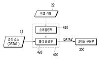
도 2는 상기 도 1의 표시 장치의 제어부(400)에 포함되어 영상 소스 데이터(DATA1)의 영상 보상을 수행하는 영상 보상 시스템의 구성을 개략적으로 나타낸 블록도이다.2 is a block diagram schematically illustrating the configuration of an image compensation system included in the
도 2의 실시 예에 따른 표시 장치의 영상 보상 시스템은 제1 스케일링부(10), 보상 회로부(20), 및 제2 스케일링부(30)를 포함한다. 상기 영상 보상 시스템이 포함된 제어부(400)에서 영상 데이터의 보상 처리 후 보상된 영상 데이터 신호(DATA2)는 구동 회로부인 데이터 구동부(300)로 전달된다.The image compensation system of the display apparatus according to the embodiment of FIG. 2 includes a
유기 발광 다이오드(OLED)와 같은 자발광 소자를 포함하는 화소로 구성된 표시부(100)를 포함하는 표시 장치는 전압 또는 전류를 유기 발광 다이오드를 통해 흐르는 다른 구동 전류로 변환하여 영상을 표시한다. 유기 발광 다이오드(OLED)를 발광시키는 구동 전류는 영상 데이터 신호에 대응하여 결정된다. 표시 장치는 외부의 영상 소스를 통해 들어온 영상 소스 데이터로부터 처리하여 상기 영상 데이터 신호를 생성한다. A display device including a
상기 영상 소스 데이터는 휘도 또는 색좌표 등 화소의 영상 표시에 관련된 다양한 정보를 포함하고 있다. 표시 장치의 표시부 특성으로 인해 이러한 영상 소스 데이터들이 가지고 있는 휘도 또는 색좌표의 영상 정보들이 정확하게 표현되지 못할 수가 있다. 동일한 휘도 또는 색좌표 정보임에도 불구하고 표시부에 포함된 화소의 특성에 따라 불규칙적으로 다양하게 열화 또는 노화가 발현되기 때문이다. The image source data includes various information related to image display of pixels such as luminance or color coordinates. Due to the characteristics of the display unit of the display device, the image information of the brightness or color coordinates of these image source data may not be accurately displayed. This is because, despite the same luminance or color coordinate information, various deterioration or aging is irregularly generated depending on the characteristics of the pixels included in the display portion.
이러한 휘도 불균일을 해결하기 위해서 종래 표시 장치에서는 화소의 특성 정보를 이용하여 원본의 영상 데이터를 보상함으로써 영상 데이터에 따라 이상적으로 발현되어야 할 목적 휘도(타겟 휘도)로 표시될 수 있도록 영상 처리한다. 그러나, 이는 화소의 특성 정보를 측정한 특정 밝기의 조건 하에서만 정확한 보상이 이루어질 뿐, 표시 장치의 외부 환경에 따라 다른 밝기 조건 하에서는 정확한 보상이 되지 않는다.In order to solve such luminance unevenness, the conventional display device performs image processing so as to display the target image data (target luminance) to be ideally expressed according to the image data by compensating the original image data using the characteristic information of the pixel. However, this compensation is performed only under the condition of the specific brightness at which the characteristic information of the pixel is measured, but is not compensated correctly under different brightness conditions depending on the external environment of the display device.
따라서, 본 발명의 일 실시 예에 따른 영상 보상 시스템은 어떠한 외부 환경의 밝기 조건 하에서도 유연하게 휘도 보상이 적용될 수 있도록 구성된다. Therefore, the image compensation system according to an embodiment of the present invention is configured so that the luminance compensation can be flexibly applied even under the brightness condition of any external environment.
도 2에서와 같이 본 발명의 일 실시 예에 따른 제어부(400)에 영상 보상 시스템을 구비한다. 상기 영상 보상 시스템은 보상 회로부(20)의 전단에 제1 스케일링부(10)를 포함하고, 후단에 제2 스케일링부(30)를 더 포함하여 데이터를 가공처리 한다.As shown in FIG. 2, the
먼저, 제1 스케일링부(10)는 외부 영상 소스로부터 최초로 전달되는 영상 소스 데이터(DATA1)(1)를 전달받아 소정의 데이터 가공 처리를 수행한다. 이하, 제1 스케일링부(10)에서 이루어지는 영상 데이터의 처리 과정을 제1 보상이라 한다.First, the
외부에서 공급되는 영상 소스 데이터(1)는 표시 영상에 대한 휘도 데이터를 포함한다. 상기 제1 보상 과정은 영상 소스 데이터(DATA1)(1)의 휘도 데이터를 1차적으로 조정하여 변환하여 제1 보상 데이터(SDATA1)를 생성하는 과정이다. The
즉, 제1 스케일링부(10)는 소정의 기준 밝기에 따라 입력되는 영상 소스 데이터(1)를 조정한다. 이때 기준 밝기는 표시 장치에서 소정의 픽셀 정보(2)가 측정될 때의 밝기를 의미한다.That is, the
구체적으로 상기 제1 보상 과정은 도 3에 도시된 그래프로 설명될 수 있다. 도 3의 그래프는 영상 신호의 계조 데이터(gray)에 대한 휘도값(L)의 관계를 표시한 그래프이다.Specifically, the first compensation process can be described with the graph shown in FIG. The graph of Fig. 3 is a graph showing the relationship of the luminance value (L) to the gray-scale data (gray) of the video signal.
도 3의 그래프를 참조하여 알 수 있듯이, 제1 스케일링부(10)에 입력되는 영상 소스 데이터(1)의 계조 데이터는 g 값을 가지는데, 제1 스케일링부(10)는 제1 보상 수식을 적용하여 조정된 계조 데이터(scaled gray data)인 g'값으로 변환시키게 된다. 이것은 현재 입력되는 영상 소스 데이터의 계조 데이터를 픽셀 정보가 측정되는 밝기 조건에 대응하는 값으로 변경시키는 것이다. 즉, 소정의 휘도값 L1을 표시하는 현재 입력되는 영상 소스 데이터의 계조 데이터 g를, 동일한 휘도값 L1을 표시하는 픽셀 정보 측정시의 기준 밝기 조건에 대응하는 계조 데이터 g'로 변환시킨다. 도 3의 그래프를 보면, 제1 스케일링부(10)의 보상으로 인해 계조-휘도간 관계 곡선이 (a)에서 (b)의 곡선으로 이동한 것이어서, 표시 장치의 표시부는 영상 소스 데이터가 입력되는 현재 상태의 밝기보다 더 밝은 휘도로 변경될 수 있다.3, the grayscale data of the
제1 스케일링부(10)는 픽셀 정보의 측정시 밝기 조건에 대응하여 계조 데이터를 조정하는 제1 보상 수식이 적용될 수 있는 회로 소자로 구성된 연산 회로일 수 있으며, 구체적인 연산 회로는 다양하게 설계될 수 있으므로 이에 대한 설명은 생략하기로 한다.The
제1 스케일링부(10)에서 적용하는 제1 보상 수식은 다음 수학식 1과 같다.The first compensation formula applied by the
(수학식 1)(1)
![]()
![]()
여기서, g'는 조정된 계조 데이터인 제1 보상 데이터, g는 영상 소스 데이터(1)의 계조 데이터, R brt는 표시 장치에서 픽셀 정보의 측정시 기준 밝기, N brt는 표시 장치의 표시부가 설정한 현재의 특정 밝기, γ는 표시부 고유의 감마값이다.Where g 'is the first compensation data, which is the adjusted tone data, g is the tone data of the image source data (1), R brt is the reference brightness at the time of measuring pixel information in the display device, The current specific brightness, gamma, is the gamma value inherent in the display portion.
제1 스케일링부(10)에서 조정된 제1 보상 데이터(SDATA1)는 보상 회로부(20)에 전달된다. 보상 회로부(20)에서는 표시 장치의 표시부에서 측정한 픽셀 정보(2)를 이용하여 입력된 제1 보상 데이터(SDATA1)에 대하여 소정의 데이터 가공 처리를 수행한다. 이때 보상 회로부(20)에서 표시 장치의 휘도 불균일성에 관한 보상을 수행하는데, 이하, 이러한 영상 데이터의 처리 과정을 제2 보상이라 한다.The first compensation data SDATA1 adjusted by the
보상 회로부(20)는 제2 보상 과정을 통해 입력된 제1 보상 데이터(SDATA1)를 보상하여 제2 보상 데이터(SDATA2)를 출력한다. 여기서 보상 회로부(20)는 소정의 기 설정된 기준 밝기 하에서 측정한 픽셀 정보(2)를 이용한다.The
픽셀 정보(2)는 표시부를 구성하는 화소의 재료, 제조 환경, 구조적 특성으로 인해 원래의 계조 데이터가 출력하는 휘도값이 목표 휘도값에 대비하여 벗어나는 정도, 즉 휘도 차이를 보상하는 파라미터를 의미한다. 따라서 픽셀 정보(2)의 파라미터는 특정되지 않으며, 다양한 변수로 측정될 수 있다. 상기 픽셀 정보는 모든 화소에 대하여 측정할 수는 없고 대표적인 지점에 위치하는 화소를 선택적으로 지정하여 그에 대한 특성 정보를 취득할 수 있다.The
보상 회로부(20)는 상기 픽셀 정보(2)를 이용하여 실제 표시되는 휘도값을 계조 데이터의 목표 휘도값에 일치하도록 보정하는 것이므로 특정의 회로 구성에 한정되지 않고 다양하게 구성할 수 있다. The
구체적으로 상기 제2 보상 과정은 도 4에 도시된 그래프로 설명할 수 있다. 도 4의 그래프를 참조하여 알 수 있듯이, 보상 회로부(20)에 입력되는 제1 보상 데이터(SDATA1)는 이미 도 3의 그래프에서 본 바와 같이 제1 스케일링부(10)의 변환에 의해 기준 밝기에 근거한 g'의 계조값을 가진다. 그리고 휘도값 L1의 밝기로 표시되는데, 보상 회로부(20)는 표시 장치에서 측정된 픽셀 정보를 이용하여 제2 보상 데이터(SDATA2)로 변조한다.Specifically, the second compensation process can be illustrated by the graph shown in FIG. As can be seen from the graph of FIG. 4, the first compensation data SDATA1 inputted to the
보상 회로부(20)는 g' 계조값에 대응하는 현재 휘도가 L1일 때 목표 휘도값인 L2로 표시되도록 g' 계조값을 보상하여 g'_mod로 변환한다.The
도 4의 그래프에 따르면, 보상 회로부(20)에서 처리되는 제2 보상 과정은 픽셀 정보의 측정 당시 기준 밝기의 조건인 (b) 곡선을 따라 목표 휘도값 L2로 변환되는 과정이다.According to the graph of FIG. 4, the second compensation process performed in the
보상 회로부(20)에서 제2 보상을 통해 출력되는 제2 보상 데이터(SDATA2)는 제2 스케일링부(30)로 전달된다.The second compensation data SDATA2 outputted through the second compensation in the
제2 스케일링부(30)는 계조 데이터에 대응하는 타겟 휘도값으로 보상된 영상 데이터에 대하여 다시 원래 표시부의 현재 밝기에 따라 재변조하는 데이터 가공 처리를 수행한다. 이하, 제2 스케일링부(30)에서 이루어지는 영상 데이터의 처리 과정을 제3 보상이라 한다.The
즉, 보상 회로부(20)에서 픽셀 정보의 측정 당시 밝기인 기준 밝기에 대응하여 타겟 휘도값으로 출력되도록 보상한 제2 보상 데이터(SDATA2)를 입력받은 제2 스케일링부(30)는 소정의 수식을 적용하여 현재 표시부의 설정된 밝기에 따라 다시 변형하여 제3 보상 데이터(DATA2)로 출력한다.That is, the
구체적으로 상기 제3 보상 과정은 도 5의 그래프로 설명될 수 있다.Specifically, the third compensation process can be described by the graph of FIG.
도 5의 그래프를 참조하여 알 수 있듯이, 제2 스케일링부(30)에 입력되는 제2 보상 데이터(SDATA2)의 계조 데이터는 휘도 보상의 제2 보상 과정을 거쳐 g'_mod 값을 가지는데, 제2 스케일링부(30)는 제2 보상 수식을 적용하여 재조정된 계조 데이터인 g_mod값으로 변환시키게 된다.5, the gradation data of the second compensation data SDATA2 input to the
이것은 픽셀 정보가 측정되는 기준 밝기에 대응하여 타겟 휘도값으로 정확하게 표시되도록 보상된 계조 데이터를 본래의 표시부의 현재 밝기 조건에 대응하는 값으로 다시 변경시키는 것이다. 즉, 소정의 타겟 휘도값 L2로 보상된 제2 보상 데이터(SDATA2)의 g'_mod 계조값을 동일한 타겟 휘도값 L2를 표시하는 현재 표시부의 밝기 조건에 대응하는 g_mod 계조값으로 변환시킨다.This is to change the compensated gradation data back to a value corresponding to the current brightness condition of the original display unit so that the pixel information is correctly displayed as the target brightness value corresponding to the reference brightness at which the pixel information is measured. That is, the g'_mod gradation value of the second compensation data SDATA2 compensated by the predetermined target luminance value L2 is converted into the g_mod gradation value corresponding to the brightness condition of the current display unit which displays the same target luminance value L2.
도 5의 그래프를 보면, 제2 스케일링부(30)의 보상으로 인해 계조-휘도간 관계 곡선이 (b)에서 (a)의 곡선으로 이동함을 알 수 있다. 이는 본 발명의 실시 예에 따른 영상 보상 시스템을 통한 영상 데이터 보상 이전에 표시부의 원래 밝기 조건에 대응하는 관계 곡선인 (a) 곡선으로 다시 변경되었음을 의미한다.Referring to the graph of FIG. 5, it can be seen that the gradation-luminance relationship curve is shifted from the curve (b) to the curve (a) due to the compensation of the
제2 스케일링부(30)는 원래 표시부의 현재 밝기 조건에 대응하여 계조 데이터를 재조정하는 제2 보상 수식이 적용될 수 있는 회로 소자로 구성된 연산 회로일 수 있으며, 구체적인 연산 회로는 다양하게 설계될 수 있으므로 이에 대한 설명은 생략하기로 한다.The
제2 스케일링부(30)에서 적용하는 제2 보상 수식은 다음 수학식 2와 같다.The second compensation formula applied by the
(수학식 2)(2)
![]()
![]()
여기서, g_mod는 재조정된 계조 데이터인 제3 보상 데이터, g'_mod는 보상 회로부(20)에서 보상된 제2 보상 데이터, R brt는 표시 장치에서 픽셀 정보의 측정시 기준 밝기, N brt는 표시 장치의 표시부가 설정한 현재의 특정 밝기, γ는 표시부 고유의 감마값이다.G_mod is third compensation data which is readjusted gradation data, g'_mod is second compensation data compensated by the
상기 수학식 2는 상기 수학식 1에서 데이터의 조정을 위해 곱해주는 보상율(![]()
![]()
![]()
![]()
이렇게 출력된 제3 보상 데이터(DATA2)는 표시 장치의 구동 회로인 데이터 구동부(300)로 전달된다.The third compensation data DATA2 thus outputted is transmitted to the
데이터 구동부(300)로 전달된 상기 제3 보상 데이터(DATA2)에 따른 데이터 전압은 표시부(100)의 각 화소에 전달되는 스캔 신호에 응답하여 동작이 활성화되는 대응하는 화소에 전달된다.The data voltage according to the third compensation data DATA2 transmitted to the
데이터 구동부(300)에 전달되는 제3 보상 데이터(DATA2)는 표시 장치에 최초 입력되는 영상 소스 데이터에 대응하는 목적 휘도(타겟 휘도)로 표시될 수 있도록 데이터를 보상하는 보상 회로부(20)의 동작 전후에, 현재 표시 장치의 표시부의 밝기에 대응하여 데이터 보상을 적용한 출력 데이터이므로 이에 따른 표시 영상은 표시 장치의 밝기 조건과 무관하게 균일하고 정확한 휘도로 표시될 수 있다.The third compensation data DATA2 transmitted to the
도 6은 도 1의 표시 장치 중 제어부(400)에 포함된 본 발명의 다른 일 실시 예에 따른 표시 장치의 영상 보상 시스템의 구성을 개략적으로 나타낸 블록도이다.6 is a block diagram schematically showing the configuration of an image compensation system of a display device according to another embodiment of the present invention included in the
도 6에 따른 표시 장치의 영상 보상 시스템은, 도 1의 실시 예와 달리, 보상 회로부(420) 및 상기 보상 회로부의 전단에 연결된 적어도 하나의 스케일링부(410)을 포함한다. 그래서 제어부(400)에 입력되는 영상 소스 데이터를 보상 처리한 후 보상된 영상 데이터 신호를 생성하여 상기 보상 회로부의 후단에 연결된 데이터 구동부(300)로 전달한다.Unlike the embodiment of FIG. 1, the image compensation system of the display device according to FIG. 6 includes a
도 6의 실시 예에 따른 영상 보상 시스템에서 외부의 영상 소스를 통해 들어온 영상 소스 데이터(DATA1')(11)는 보상 회로부(420)에 전달된다.In the image compensation system according to the embodiment of FIG. 6, the image source data (DATA1 ') 11 inputted through an external image source is transmitted to the
보상 회로부(420)는 스케일링부(410)에 연결되어 있는데, 스케일링부(410)를 통해 전달되는 픽셀 정보(22)를 이용하여 상기 영상 소스 데이터(11)를 보상하여 보상 데이터(DATA2')를 출력한다.The
여기서 상기 픽셀 정보(22)는 소정의 기 설정된 기준 밝기에서 측정된 데이터 보상을 위한 파라미터이다. 즉, 픽셀 정보(22)는 표시부를 구성하는 화소의 재료, 제작 환경, 구조적 특성으로 인해 원래의 계조 데이터가 출력하는 휘도값이 목표 휘도값에 대비하여 벗어나는 휘도 차를 보상하기 위한 파라미터인데, 도 5의 실시 예에서는 상기 픽셀 정보(22)를 스케일링부(410)에 전달한다.Here, the
스케일링부(410)는 상기 전달받은 기준 밝기 하에서 측정된 픽셀 정보(22)를 표시 장치의 표시부의 현재 밝기에 대응하는 값으로 변환한다. 스케일링부(410)의 픽셀 정보 변환을 위한 수식은 특별히 제한되지 않으며, 스케일링부(100)는 이러한 수식을 적용하기 위한 다양한 연산 회로로 구성될 수 있다.The
이렇게 변환된 픽셀 정보는 보상 회로부(420)에 전달되고, 보상 회로부(420)는 현재 표시부의 밝기에 대응하여 변환된 픽셀 정보를 이용하여 영상 소스 데이터(DATA1')를 보상한다. 즉, 상기 변환된 픽셀 정보를 이용하여 실제 표시되는 휘도값을 영상 소스 데이터의 목표 휘도값에 일치하도록 보정한다. 그래서 보상 데이터(DATA2')를 생성하여 데이터 구동부(300)에 전달한다.The converted pixel information is transmitted to the
데이터 구동부(300)는 상기 도 2의 실시 예와 마찬가지로 표시부의 각 화소에 스캔 신호를 전달하여 활성화시킨 대응하는 화소 각각에 상기 보상 데이터(DATA2')에 따른 전압을 생성하여 전달할 수 있다. 데이터 구동부(300)는 상기 전달된 보상 데이터(DATA2')에 따른 데이터 전압을 표시부의 대응하는 각 화소에 전달하여 각 화소가 영상을 표시하게 한다.2, the
상기 보상 데이터(DATA2')는 표시부의 소정의 화소에 대한 기준 밝기 하에서 측정된 픽셀 정보를 표시 장치의 현재 밝기에 대응하여 수정한 픽셀 정보를 이용하여 목표 휘도를 표시할 수 있도록 보상된 것이므로, 이에 따른 표시 영상은 표시 장치의 밝기 조건과 무관하게 균일하고 정확한 휘도로 표시될 수 있다.Since the compensation data DATA2 'is compensated so that the target luminance can be displayed using the pixel information obtained by modifying the pixel information measured under the reference brightness for a predetermined pixel of the display unit in accordance with the current brightness of the display device, The display image according to the present invention can be displayed with uniform and accurate luminance irrespective of the brightness condition of the display device.
지금까지 참조한 도면과 기재된 발명의 상세한 설명은 단지 본 발명의 예시적인 것으로서, 이는 단지 본 발명을 설명하기 위한 목적에서 사용된 것이지 의미 한정이나 특허청구범위에 기재된 본 발명의 범위를 제한하기 위하여 사용된 것은 아니다. 그러므로 본 기술 분야의 통상의 지식을 가진 자라면 이로부터 용이하게 선택하여 대체할 수 있다. 또한 당업자는 본 명세서에서 설명된 구성요소 중 일부를 성능의 열화 없이 생략하거나 성능을 개선하기 위해 구성요소를 추가할 수 있다. 뿐만 아니라, 당업자는 공정 환경이나 장비에 따라 본 명세서에서 설명한 방법 단계의 순서를 변경할 수도 있다. 따라서 본 발명의 범위는 설명된 실시형태가 아니라 특허청구범위 및 그 균등물에 의해 결정되어야 한다.It is to be understood that both the foregoing general description and the following detailed description of the present invention are illustrative and explanatory only and are intended to be illustrative of the invention and are not to be construed as limiting the scope of the invention as defined by the appended claims. It is not. Therefore, those skilled in the art can readily select and substitute it. Those skilled in the art will also appreciate that some of the components described herein can be omitted without degrading performance or adding components to improve performance. In addition, those skilled in the art may change the order of the method steps described herein depending on the process environment or equipment. Therefore, the scope of the present invention should be determined by the appended claims and equivalents thereof, not by the embodiments described.
100: 표시부 200: 주사 구동부
300: 데이터 구동부 400: 제어부
500: 화소
1, 11: 영상 소스 데이터 2, 22: 픽셀 정보
10: 제1 스케일링부 20: 보상 회로부
30: 제2 스케일링부 410: 스케일링부
420: 보상 회로부100: display unit 200: scan driver
300: Data driver 400:
500: pixel
1, 11:
10: first scaling unit 20: compensation circuit
30: second scaling unit 410: scaling unit
420: compensation circuit part
Claims (14)
외부 소스로부터 상기 영상 데이터 신호를 입력 받고, 상기 복수의 화소에 대한 픽셀 정보가 측정되는 당시의 기준 밝기에 대응하여 상기 영상 데이터 신호를 보상하여 제1 보상 데이터를 생성하는 제1 스케일링부,
상기 기준 밝기 조건에서 측정된 상기 픽셀 정보를 이용하여 상기 영상 데이터 신호에 따른 타겟 휘도를 표시하도록 상기 제1 보상 데이터의 계조 데이터를 보상하고 제2 보상 데이터를 생성하는 보상 회로부,
상기 표시부의 현재 밝기에 대응하여 상기 제2 보상 데이터를 보상하여 제3 보상 데이터를 생성하는 제2 스케일링부, 및
상기 제3 보상 데이터를 상기 복수의 화소 중 활성화된 대응하는 구동 화소에 전달하여 영상을 표시하게 하는 데이터 구동부를 포함하는 표시 장치.A display device for displaying an image by transmitting a video data signal to each pixel of a display portion including a plurality of pixels,
A first scaling unit receiving the image data signal from an external source and generating first compensation data by compensating the image data signal corresponding to a reference brightness at the time when pixel information for the plurality of pixels is measured,
A compensation circuit for compensating the gray level data of the first compensation data and generating second compensation data to display the target brightness according to the video data signal using the pixel information measured under the reference brightness condition,
A second scaling unit for compensating for the second compensation data corresponding to the current brightness of the display unit to generate third compensation data,
And a data driver for transferring the third compensation data to a corresponding driving pixel among the plurality of pixels to display an image.
상기 제1 스케일링부 및 상기 제2 스케일링부는 상기 기준 밝기에 대한 상기 표시부의 현재 밝기의 비율을 반영한 보상율을 이용하여 계산하는 연산 회로인 것을 특징으로 하는 표시 장치.The method according to claim 1,
Wherein the first scaling unit and the second scaling unit are arithmetic circuits that calculate using a compensation rate that reflects a ratio of the current brightness of the display unit to the reference brightness.
상기 제1 스케일링부는 상기 영상 데이터 신호에 상기 기준 밝기에 대한 상기 표시부의 현재 밝기의 비율을 반영한 보상율을 곱하여 상기 제1 보상 데이터를 생성하고,
상기 제2 스케일링부는 상기 제2 보상 데이터에 상기 보상율을 나누어 상기 제3 보상 데이터를 생성하는 것을 특징으로 하는 표시 장치. The method according to claim 1,
Wherein the first scaling unit multiplies the image data signal by a compensation factor reflecting the ratio of the current brightness of the display unit to the reference brightness to generate the first compensation data,
Wherein the second scaling unit divides the compensation rate by the second compensation data to generate the third compensation data.
상기 픽셀 정보는 상기 복수의 화소에 대한 재료, 구조, 제조 환경 특성으로 인해 상기 영상 데이터 신호의 원래 계조 데이터가 출력하는 휘도값이 상기 타겟 휘도값에 대비하여 벗어나는 휘도 차를 보상하는 파라미터인 것을 특징으로 하는 표시 장치. The method according to claim 1,
Wherein the pixel information is a parameter for compensating for a luminance difference in which the luminance value output from the original gradation data of the image data signal deviates from the target luminance value due to the material, structure, and manufacturing environment characteristics of the plurality of pixels .
상기 제1 스케일링부는 상기 보상 회로부의 전단에 연결되고, 상기 제2 스케일링부는 상기 보상 회로부의 후단에 연결되는 표시 장치. The method according to claim 1,
Wherein the first scaling unit is connected to a front end of the compensation circuit unit and the second scaling unit is connected to a rear end of the compensation circuit unit.
상기 표시 장치는, 상기 복수의 화소 각각에 대응하는 스캔 신호를 전달하여 상기 복수의 화소 각각을 순차적으로 활성화하는 주사 구동부, 및 상기 외부 소스로부터 상기 영상 데이터 신호와 이의 영상 표시를 제어하는 제어 입력 신호를 수신하여 상기 영상 데이터 신호를 가공 처리하는 제어부를 더 포함하고,
상기 제어부는 상기 제1 스케일링부, 보상 회로부, 및 제2 스케일링부를 포함하는 것을 특징으로 하는 표시 장치. The method according to claim 1,
The display device includes a scan driver for sequentially transmitting a scan signal corresponding to each of the plurality of pixels and sequentially activating each of the plurality of pixels, and a control unit for controlling the display of the image data signal and the control input signal Further comprising a control unit for receiving the video data signal and processing the video data signal,
Wherein the control unit includes the first scaling unit, the compensation circuit unit, and the second scaling unit.
소정의 기준 밝기 조건에서 측정된 픽셀 정보를 취득하여 상기 표시부의 현재 밝기 조건에 따라 변환하는 스케일링부,
외부 소스로부터 상기 영상 데이터 신호를 입력 받고, 상기 스케일링부에서 변환된 픽셀 정보를 이용하여 상기 영상 데이터 신호에 따른 타겟 휘도를 표시하도록 상기 영상 데이터 신호를 보상하여 출력 영상 데이터 신호를 생성하는 보상 회로부, 및
상기 출력 영상 데이터 신호를 상기 복수의 화소 중 활성화된 대응하는 구동 화소에 전달하여 영상을 표시하게 하는 데이터 구동부를 포함하는 표시 장치. A display device for displaying an image by transmitting a video data signal to each pixel of a display portion including a plurality of pixels,
A scaling unit for obtaining pixel information measured at a predetermined reference brightness condition and converting the acquired pixel information according to a current brightness condition of the display unit,
A compensation circuit for receiving the image data signal from an external source and compensating the image data signal to display a target luminance according to the image data signal using the pixel information converted by the scaling unit to generate an output image data signal, And
And a data driver for transmitting the output image data signal to a corresponding driving pixel among the plurality of pixels to display an image.
상기 픽셀 정보는 상기 복수의 화소에 대한 재료, 구조, 제조 환경 특성으로 인해 상기 영상 데이터 신호의 원래 계조 데이터가 출력하는 휘도값이 상기 타겟 휘도값에 대비하여 벗어나는 휘도 차를 보상하는 파라미터인 것을 특징으로 하는 표시 장치. 8. The method of claim 7,
Wherein the pixel information is a parameter for compensating for a luminance difference in which the luminance value output from the original gradation data of the image data signal deviates from the target luminance value due to the material, structure, and manufacturing environment characteristics of the plurality of pixels .
상기 표시 장치는, 상기 복수의 화소 각각에 대응하는 스캔 신호를 전달하여 상기 복수의 화소 각각을 순차적으로 활성화하는 주사 구동부, 및 상기 외부 소스로부터 상기 영상 데이터 신호와 이의 영상 표시를 제어하는 제어 입력 신호를 수신하여 상기 영상 데이터 신호를 가공 처리하는 제어부를 더 포함하고,
상기 제어부는, 스케일링부 및 보상 회로부를 포함하는 것을 특징으로 하는 표시 장치. 8. The method of claim 7,
The display device includes a scan driver for sequentially transmitting a scan signal corresponding to each of the plurality of pixels and sequentially activating each of the plurality of pixels, and a control unit for controlling the display of the image data signal and the control input signal Further comprising a control unit for receiving the video data signal and processing the video data signal,
Wherein the control unit includes a scaling unit and a compensation circuit unit.
소정의 기준 밝기 조건에서 상기 복수의 화소에 대한 픽셀 정보를 측정하는 단계,
상기 기준 밝기에 대한 상기 표시부의 현재 밝기의 비율을 반영한 보상율을 계산하는 단계,
외부 소스로부터 입력된 상기 영상 데이터 신호에 상기 보상율을 적용하여 상기 기준 밝기에 대응하는 제1 보상을 수행하는 단계,
상기 제1 보상에 따른 제1 출력 데이터에 대해 상기 픽셀 정보를 이용하여 상기 영상 데이터 신호에 따른 타겟 휘도를 표시하도록 계조 데이터의 제2 보상을 수행하는 단계,
상기 제2 보상에 따른 제2 출력 데이터에 상기 보상율을 적용하여 상기 표시부의 현재 밝기에 대응하는 제3 보상을 수행하는 단계, 및
상기 제3 보상에 따른 제3 출력 데이터를 상기 복수의 화소 각각에 전달하여 영상을 표시하는 단계를 포함하는 영상 보상 방법. An image compensation method for compensating for a video data signal in a display device for displaying an image by transmitting a video data signal to each pixel of a display unit including a plurality of pixels,
Measuring pixel information for the plurality of pixels at a predetermined reference brightness condition,
Calculating a compensation rate that reflects a ratio of the current brightness of the display unit to the reference brightness,
Performing a first compensation corresponding to the reference brightness by applying the compensation factor to the image data signal input from an external source,
Performing a second compensation of the gradation data to display a target luminance according to the image data signal using the pixel information for the first output data according to the first compensation,
Performing a third compensation corresponding to the current brightness of the display unit by applying the compensation factor to second output data according to the second compensation, and
And transmitting third output data according to the third compensation to each of the plurality of pixels to display an image.
상기 제1 보상을 수행하는 단계는 상기 영상 데이터 신호에 상기 보상율을 곱셈 연산하는 단계이고,
상기 제3 보상을 수행하는 단계는 상기 제2 출력 데이터에 상기 보상율을 나눗셈 연산하는 단계인 영상 보상 방법. 11. The method of claim 10,
Wherein the step of performing the first compensation is a step of multiplying the image data signal by the compensation factor,
Wherein performing the third compensation is a step of performing a division operation on the second output data with the compensation rate.
상기 픽셀 정보는 상기 복수의 화소에 대한 재료, 구조, 제조 환경 특성으로 인해 상기 영상 데이터 신호의 원래 계조 데이터가 출력하는 휘도값이 상기 타겟 휘도값에 대비하여 벗어나는 휘도 차를 보상하는 파라미터인 것을 특징으로 하는 영상 보상 방법. 11. The method of claim 10,
Wherein the pixel information is a parameter for compensating for a luminance difference in which the luminance value output from the original gradation data of the image data signal deviates from the target luminance value due to the material, structure, and manufacturing environment characteristics of the plurality of pixels / RTI >
소정의 기준 밝기 조건에서 상기 복수의 화소에 대한 픽셀 정보를 측정하는 단계,
상기 픽셀 정보를 취득하여 상기 표시부의 현재 밝기 조건에 따라 상기 픽셀 정보를 변환하는 단계,
외부 소스로부터 입력된 상기 영상 데이터 신호에 대해 상기 변환된 픽셀 정보를 이용하여 상기 영상 데이터 신호에 따른 타겟 휘도를 표시하도록 보상하는 단계, 및
상기 보상 단계에서 보상된 상기 영상 데이터 신호의 보상 데이터 신호를 상기 복수의 화소 각각에 전달하여 영상을 표시하는 단계를 포함하는 영상 보상 방법. An image compensation method for compensating for a video data signal in a display device for displaying an image by transmitting a video data signal to each pixel of a display unit including a plurality of pixels,
Measuring pixel information for the plurality of pixels at a predetermined reference brightness condition,
Acquiring the pixel information and converting the pixel information according to a current brightness condition of the display unit;
Compensating for the image data signal inputted from an external source to display the target luminance according to the image data signal using the converted pixel information, and
And transmitting the compensated data signal of the compensated image data signal to each of the plurality of pixels to display an image.
상기 픽셀 정보는 상기 복수의 화소에 대한 재료, 구조, 제조 환경 특성으로 인해 상기 영상 데이터 신호의 원래 계조 데이터가 출력하는 휘도값이 상기 타겟 휘도값에 대비하여 벗어나는 휘도 차를 보상하는 파라미터인 것을 특징으로 하는 영상 보상 방법. 14. The method of claim 13,
Wherein the pixel information is a parameter for compensating for a luminance difference in which the luminance value output from the original gradation data of the image data signal deviates from the target luminance value due to the material, structure, and manufacturing environment characteristics of the plurality of pixels / RTI >
Priority Applications (2)
| Application Number | Priority Date | Filing Date | Title |
|---|---|---|---|
| KR1020130057812A KR102046443B1 (en) | 2013-05-22 | 2013-05-22 | Display device and method for compensation of image data of the same |
| US14/062,656 US9153175B2 (en) | 2013-05-22 | 2013-10-24 | Display device and method for compensation of image data of the same |
Applications Claiming Priority (1)
| Application Number | Priority Date | Filing Date | Title |
|---|---|---|---|
| KR1020130057812A KR102046443B1 (en) | 2013-05-22 | 2013-05-22 | Display device and method for compensation of image data of the same |
Publications (2)
| Publication Number | Publication Date |
|---|---|
| KR20140137191A true KR20140137191A (en) | 2014-12-02 |
| KR102046443B1 KR102046443B1 (en) | 2019-11-20 |
Family
ID=51935110
Family Applications (1)
| Application Number | Title | Priority Date | Filing Date |
|---|---|---|---|
| KR1020130057812A KR102046443B1 (en) | 2013-05-22 | 2013-05-22 | Display device and method for compensation of image data of the same |
Country Status (2)
| Country | Link |
|---|---|
| US (1) | US9153175B2 (en) |
| KR (1) | KR102046443B1 (en) |
Cited By (1)
| Publication number | Priority date | Publication date | Assignee | Title |
|---|---|---|---|---|
| CN112542142A (en) * | 2020-12-02 | 2021-03-23 | Tcl华星光电技术有限公司 | Compensation method and compensation device of display panel |
Families Citing this family (10)
| Publication number | Priority date | Publication date | Assignee | Title |
|---|---|---|---|---|
| US9740046B2 (en) * | 2013-11-12 | 2017-08-22 | Nvidia Corporation | Method and apparatus to provide a lower power user interface on an LCD panel through localized backlight control |
| US9462239B2 (en) * | 2014-07-15 | 2016-10-04 | Fuji Xerox Co., Ltd. | Systems and methods for time-multiplexing temporal pixel-location data and regular image projection for interactive projection |
| KR102357378B1 (en) * | 2015-07-07 | 2022-02-03 | 삼성디스플레이 주식회사 | Image processing device and display device having the same |
| CN106057130B (en) * | 2016-08-18 | 2018-09-21 | 上海天马有机发光显示技术有限公司 | A kind of compensation method of display panel and display panel |
| CN107657916B (en) * | 2017-09-26 | 2020-05-08 | 惠科股份有限公司 | Method, structure and restoration system for generating image compensation signal |
| KR102423637B1 (en) * | 2017-10-27 | 2022-07-22 | 삼성디스플레이 주식회사 | Display apparatus and method of driving the same |
| TWI716120B (en) * | 2019-09-25 | 2021-01-11 | 友達光電股份有限公司 | Pixel circuit and display panel |
| TWI764574B (en) * | 2020-03-16 | 2022-05-11 | 瑞鼎科技股份有限公司 | Front-end processing circuit in front of panel driving circuit |
| CN112700746B (en) * | 2020-12-31 | 2022-10-04 | 深圳Tcl数字技术有限公司 | Brightness adjusting method of display device, terminal device and storage medium |
| WO2024000322A1 (en) * | 2022-06-29 | 2024-01-04 | 京东方科技集团股份有限公司 | Timing controller and detection compensation method therefor, and display panel |
Family Cites Families (9)
| Publication number | Priority date | Publication date | Assignee | Title |
|---|---|---|---|---|
| GB0323281D0 (en) | 2003-10-04 | 2003-11-05 | Koninkl Philips Electronics Nv | Improving grey scale contrast in a 3D image display device |
| JP4222340B2 (en) * | 2004-09-22 | 2009-02-12 | ソニー株式会社 | Image display device and brightness correction method in image display device |
| CA2504571A1 (en) | 2005-04-12 | 2006-10-12 | Ignis Innovation Inc. | A fast method for compensation of non-uniformities in oled displays |
| TWI296483B (en) * | 2005-12-07 | 2008-05-01 | Marketech Int Corp | Apparatus and method for adjusting input image based on characteristics of display system |
| TWI466093B (en) | 2007-06-26 | 2014-12-21 | Apple Inc | Management techniques for video playback |
| KR101443371B1 (en) * | 2007-07-13 | 2014-09-29 | 엘지디스플레이 주식회사 | Liquid crystal display device and driving method of the same |
| KR101352966B1 (en) | 2007-07-30 | 2014-01-22 | 삼성디스플레이 주식회사 | Organic light emitting display device and driving method thereof |
| KR20090081849A (en) * | 2008-01-25 | 2009-07-29 | 삼성전자주식회사 | Display appratus and method of driving the same |
| KR20110102697A (en) | 2010-03-11 | 2011-09-19 | 엘지전자 주식회사 | Apparatus for displaying image and method for operating the same |
-
2013
- 2013-05-22 KR KR1020130057812A patent/KR102046443B1/en active IP Right Grant
- 2013-10-24 US US14/062,656 patent/US9153175B2/en active Active
Cited By (2)
| Publication number | Priority date | Publication date | Assignee | Title |
|---|---|---|---|---|
| CN112542142A (en) * | 2020-12-02 | 2021-03-23 | Tcl华星光电技术有限公司 | Compensation method and compensation device of display panel |
| CN112542142B (en) * | 2020-12-02 | 2022-04-01 | Tcl华星光电技术有限公司 | Compensation method and compensation device of display panel |
Also Published As
| Publication number | Publication date |
|---|---|
| KR102046443B1 (en) | 2019-11-20 |
| US9153175B2 (en) | 2015-10-06 |
| US20140347403A1 (en) | 2014-11-27 |
Similar Documents
| Publication | Publication Date | Title |
|---|---|---|
| KR102046443B1 (en) | Display device and method for compensation of image data of the same | |
| CN109599060B (en) | Pixel compensation method, pixel compensation system and display device | |
| KR102049089B1 (en) | Apparatus for compensating color characteristic in a display device and compensating method | |
| KR101850994B1 (en) | Method for controlling brightness in a display device and the display device using the same | |
| JP5026293B2 (en) | Organic electroluminescent display device and driving method thereof | |
| KR102034062B1 (en) | Organic light emitting diode display device and method for driving the same | |
| KR102071056B1 (en) | Display device and method for compensation of image data of the same | |
| KR20170051630A (en) | Luminance control device and display device including the same | |
| KR102138590B1 (en) | Apparatus and Method for Generating of Luminance Correction Data | |
| US9336706B2 (en) | Organic light-emitting diode (OLED) display and method for driving the same | |
| KR20110011592A (en) | Display device, and manufacturing method and control method thereof | |
| KR20140056799A (en) | Display device, apparatus for compensating degradation and method teherof | |
| KR20100046500A (en) | Organic light emitting device, and apparatus and method of generating modification information therefor | |
| KR20120028007A (en) | Luminance correction system for organic light emitting display device | |
| KR20140116690A (en) | Display device, data processing device for the same and method thereof | |
| US9153176B2 (en) | Display device and method of driving the same | |
| JP2010048939A (en) | Display apparatus, display control apparatus, and display control method as well as program | |
| KR101957758B1 (en) | Organic light emitting diode display and driving method thereof | |
| KR20160019588A (en) | Display apparatus and display method | |
| JP2004252409A (en) | Image display device | |
| KR20110005639A (en) | Self light emitting display device and method for driving self light emitting display device | |
| CN109949750B (en) | Display device and driving method thereof | |
| CN111583869A (en) | Display device | |
| KR20170072994A (en) | Organic light emitting display, device and method for driving the same | |
| KR20150071549A (en) | Display device and display device driving method using the same |
Legal Events
| Date | Code | Title | Description |
|---|---|---|---|
| A201 | Request for examination | ||
| E902 | Notification of reason for refusal | ||
| E701 | Decision to grant or registration of patent right | ||
| GRNT | Written decision to grant |