KR20140131040A - Carrier pulse width modulation method - Google Patents
Carrier pulse width modulation method Download PDFInfo
- Publication number
- KR20140131040A KR20140131040A KR1020130049853A KR20130049853A KR20140131040A KR 20140131040 A KR20140131040 A KR 20140131040A KR 1020130049853 A KR1020130049853 A KR 1020130049853A KR 20130049853 A KR20130049853 A KR 20130049853A KR 20140131040 A KR20140131040 A KR 20140131040A
- Authority
- KR
- South Korea
- Prior art keywords
- signal
- carrier
- pulse width
- width modulation
- modulation method
- Prior art date
Links
- 238000000034 method Methods 0.000 title claims abstract description 162
- 230000003247 decreasing effect Effects 0.000 claims description 12
- 230000001052 transient effect Effects 0.000 abstract description 21
- 230000004044 response Effects 0.000 abstract description 18
- 230000000694 effects Effects 0.000 abstract description 9
- 230000006872 improvement Effects 0.000 abstract description 4
- 238000005070 sampling Methods 0.000 description 12
- 238000006243 chemical reaction Methods 0.000 description 8
- 230000010354 integration Effects 0.000 description 7
- 230000007935 neutral effect Effects 0.000 description 7
- 238000005516 engineering process Methods 0.000 description 5
- 230000006870 function Effects 0.000 description 5
- 238000012546 transfer Methods 0.000 description 5
- 238000012937 correction Methods 0.000 description 4
- 239000004065 semiconductor Substances 0.000 description 4
- 230000001360 synchronised effect Effects 0.000 description 4
- 239000003990 capacitor Substances 0.000 description 3
- 238000013461 design Methods 0.000 description 2
- 238000012986 modification Methods 0.000 description 2
- 230000004048 modification Effects 0.000 description 2
- 230000003044 adaptive effect Effects 0.000 description 1
- 230000008901 benefit Effects 0.000 description 1
- 239000000969 carrier Substances 0.000 description 1
- 238000004891 communication Methods 0.000 description 1
- 230000000052 comparative effect Effects 0.000 description 1
- 230000005484 gravity Effects 0.000 description 1
- 238000006386 neutralization reaction Methods 0.000 description 1
- 230000010355 oscillation Effects 0.000 description 1
- 238000001228 spectrum Methods 0.000 description 1
- 230000000087 stabilizing effect Effects 0.000 description 1
- 230000009466 transformation Effects 0.000 description 1
- 238000004804 winding Methods 0.000 description 1
Images


Classifications
-
- H—ELECTRICITY
- H02—GENERATION; CONVERSION OR DISTRIBUTION OF ELECTRIC POWER
- H02M—APPARATUS FOR CONVERSION BETWEEN AC AND AC, BETWEEN AC AND DC, OR BETWEEN DC AND DC, AND FOR USE WITH MAINS OR SIMILAR POWER SUPPLY SYSTEMS; CONVERSION OF DC OR AC INPUT POWER INTO SURGE OUTPUT POWER; CONTROL OR REGULATION THEREOF
- H02M3/00—Conversion of dc power input into dc power output
- H02M3/02—Conversion of dc power input into dc power output without intermediate conversion into ac
- H02M3/04—Conversion of dc power input into dc power output without intermediate conversion into ac by static converters
- H02M3/10—Conversion of dc power input into dc power output without intermediate conversion into ac by static converters using discharge tubes with control electrode or semiconductor devices with control electrode
- H02M3/145—Conversion of dc power input into dc power output without intermediate conversion into ac by static converters using discharge tubes with control electrode or semiconductor devices with control electrode using devices of a triode or transistor type requiring continuous application of a control signal
- H02M3/155—Conversion of dc power input into dc power output without intermediate conversion into ac by static converters using discharge tubes with control electrode or semiconductor devices with control electrode using devices of a triode or transistor type requiring continuous application of a control signal using semiconductor devices only
- H02M3/156—Conversion of dc power input into dc power output without intermediate conversion into ac by static converters using discharge tubes with control electrode or semiconductor devices with control electrode using devices of a triode or transistor type requiring continuous application of a control signal using semiconductor devices only with automatic control of output voltage or current, e.g. switching regulators
- H02M3/157—Conversion of dc power input into dc power output without intermediate conversion into ac by static converters using discharge tubes with control electrode or semiconductor devices with control electrode using devices of a triode or transistor type requiring continuous application of a control signal using semiconductor devices only with automatic control of output voltage or current, e.g. switching regulators with digital control
-
- H—ELECTRICITY
- H03—ELECTRONIC CIRCUITRY
- H03K—PULSE TECHNIQUE
- H03K7/00—Modulating pulses with a continuously-variable modulating signal
- H03K7/08—Duration or width modulation ; Duty cycle modulation
Abstract
The present invention relates to a carrier pulse width modulation method for closed loop control of almost all switching power converters. The preceding carrier pulse width modulation method has a problem that it does not operate properly when the switching ripple included in the modulation reference signal is large. The present invention provides a carrier pulse width modulation method that can operate normally even when switching ripple is large. Then, the gain of the compensator can be made as large as necessary, and the improvement effect can be obtained in almost all aspects such as the transient response speed, the tracking error and the steady state error, the burden of fine tuning, and the adaptability to system fluctuation. The present invention is based on a two-level pulse width modulation method and is extended to a multi-level pulse width modulation method and a polyphase pulse width modulation method.
Description
The present invention relates to a carrier pulse width modulation method, and more particularly to a DC-DC converter or a switching regulator such as a step-down converter, a step-up converter, a step- DC switch mode power supplies such as half-bridge converters, full-bridge converters, push-pull converters, forward converters, and flyback converters; Single-phase ac-to-dc converters such as power factor correction rectifiers and pulse width modulation converters; Single-phase DC-AC converters, such as half-bridge inverters, full-bridge inverters, push-pull inverters, pulse width modulated power amplifiers, or motor drivers; Three-phase bridge inverter or three-phase motor drive; Three phase - bridge converter; Polyphase-bridge inverter or multiphase motor drive; (Or carrier-based) pulse width modulation method for closed-loop (or feedback) control of almost all switching (or stationary) power converters, such as multiphase-to-bridge converters.
Switching power converter
Power conversion is the conversion of supplied power into the required power. This power conversion is necessary in almost all cases of using power, from a small power of several watts or less to a large power of several MW or more.
One of the important goals of power conversion is to reduce power losses and increase efficiency. The switching power converter uses a switch which is a lossless control element as a means for achieving high efficiency. Lossless switches are ideal, and actual semiconductor switching devices such as diodes and transistors have some on-state losses and switching losses. However, these days, it is a technology that can achieve efficiency of 90% or more, and in some cases, 99% or more.
Pulse width modulation method
A switch is a device that is not capable of continuous control and is only capable of on-off control (or switching). Therefore, the pulse width modulation method is used to control the output of the switching power converter. The pulse width modulation method controls the width of the 2-level pulse signal through switching so that the pulse signal approximates the modulation reference signal on average. The pulse width modulation method extends not only to the 2-level but also to the 3-level, etc. multi-level pulse width modulation method. It also extends to the multiphase pulse width modulation method.
Originally, the pulse width modulation method was developed in the middle of the 20th century for the purpose of modulation in the field of communications. Although it has been used for other purposes in the control of pulse width in switching power conversion, it respects the original term of pulse width modulation and uses it as it is.
Switching ripple by the pulse width modulation can not be avoided in the output signal. The higher the switching frequency, the smaller the size of the switching ripple. However, since the switching loss of the semiconductor switching device becomes larger, there is a limit to increase the switching frequency. When it is necessary to remove the switching ripple from the output signal, a power filter composed of a capacitor and / or an inductor is mainly used.
Closed-loop control
Another important goal of power conversion is to reduce errors and increase accuracy. In the early days of power conversion technology, mainly open-loop control was used. Closed-loop control has gradually spread since it is known that closed-loop control can improve accuracy and adaptability. In the field of power management, so-called current mode control having a so-called voltage mode control and current control loop having a voltage control loop is widely used. In motor driving, so-called current control having a current control loop is widely used. In the field, so-called vector control with synchronous coordinate transformation and current control loops is widely used.
Linear feedback control
Although closed-loop control is possible in many ways, linear feedback control is typical. The linear feedback control is a control in which an error signal obtained by subtracting the output signal from the reference signal is inputted as an input signal through a linear compensator. Linear compensators are proportional compensator, proportional-integral compensator, and proportional-integral-differential compensator.
In general, the larger the proportional gain of the compensator, the smaller the tracking error and the steady state error. And, the larger the proportional gain, the faster the transient response, under the condition that the dominant pole of the system transfer function is a mistake. If the dominant pole of the system transfer function becomes a complex pair, even if the proportional gain is increased, the transient response speed is not accelerated and the frequency of oscillation becomes large.
The integral gain also has the effect of reducing the steady-state error. The larger the integration gain and the lower the frequency, the greater the effect, and the DC steady state error becomes zero regardless of the magnitude of the integral gain. However, the disadvantage is that the order of the system increases. Basically, there is a negative effect on the transient response speed. In the condition where the dominant pole of the system transfer function is a real number, the negative influence of the transient response speed is decreased as the integral gain is increased. If the dominant pole of the system transfer function is a complex number pair, even if the integration gain is increased, the transient response speed is not accelerated and the frequency of vibration is increased.
The differential gain can be used to speed up the transient response when the dominant pole of the system transfer function is a complex pair.
A method of designing the compensator in the frequency domain is also widely used. The accuracy at any frequency is proportional to the gain of the compensator at that frequency.
Generally, the greater the gain of the compensator, the more adaptive the system will be to variations in various parameters and parameters.
Carrier pulse width modulation method
The carrier pulse width modulation method is characterized in that the width of a pulse is controlled by comparing a modulation reference signal with a carrier signal of a high frequency. Then, unless over-modulated, the width of the pulse and the magnitude of the modulation reference signal are proportional, and the switching frequency is equal to the frequency of the carrier signal. Sawtooth wave and triangle wave are mainly used as carrier signal. The carrier pulse width modulation method can be used in both open loop control and closed loop control.
Carrier pulse width modulation methods have been used since the beginning of power conversion technology because they could be implemented as analog circuits. As digital technology developed, sampling pulse width modulation methods appeared. A typical example is a spatial vector pulse width modulation method of a three-phase DC-AC power converter. However, since it is known that the time delay due to sampling of the switching period has a bad influence on the closed loop control, the role of the real time comparative carrier pulse width modulation without time delay becomes important again. The real-time comparison carrier pulse width modulation method is based on an analog implementation, but can be implemented by a digital method if the sampling period is much shorter than the switching period.
Applying the carrier pulse width modulation method to closed loop current control such as a DC-DC converter, a switching regulator, or a power factor correction rectifier is often referred to as average current mode control. Applying the carrier pulse width modulation method to the closed loop control of a DC-AC inverter or an AC-DC converter is often referred to as a suboscillation method or a ramp comparison method.
The most important advantage of the carrier pulse width modulation method is that the switching frequency can be kept constant. On the other hand, it is a disadvantage that it is difficult to satisfy characteristics such as transient response speed, steady state error, and adaptability due to limitations on the magnitude of the gain of the compensator.
Hysteresis pulse width modulation method
Another method of pulse width modulation for closed loop control is hysteresis pulse width modulation. Band pulse width modulation method, sliding mode pulse width modulation method, and the like. The hysteresis pulse width modulation method is characterized in that the width of a pulse is controlled by comparing an error signal with a predetermined allowable band. The hysteresis pulse width modulation method has excellent characteristics in terms of transient response speed, steady state error, and adaptability. However, the switching frequency is not constant and varies greatly depending on the variation of various parameters and parameters of the system. If the switching frequency is not constant, the switching power loss in the semiconductor switching element is not constant, which makes it difficult to dissipate and protect the semiconductor switching element. Although it is possible to control the size of the permissible band so that the switching frequency is constant, it is blemished that the method is complicated. It is not good for the multiphase AC converter because it can not perform multiphase synchronization and it can not be applied to the harmonic neutralization in the multiphase DC interleaved converter is another disadvantage of the hysteresis pulse width modulation method.
Fixed frequency pulse width modulation method
Another pulse width modulation method for closed loop control is a fixed (or constant) frequency pulse width modulation method. It is also called peak current mode control. The fixed frequency pulse width modulation method is characterized in that the pulse is started at a certain period of time and the pulse is ended when the error signal becomes zero. The fixed frequency pulse width modulation method has a constant switching frequency. However, if the duty ratio is larger than 0.5, low order harmonics are generated due to instability, and half tracking error and steady state error of the switching ripple occur. The addition of the compensating inclined wave makes it possible to stabilize even when the duty ratio is larger than 0.5. However, the magnitude of follow-up error and steady-state error becomes larger. Adding an integral compensator eliminates DC steady-state error. The larger the integration gain, the less tracking error and the steady-state error of low frequency are often not satisfactory. It is also a burden to properly tune the integral gain in practical applications.
Fixed off-time pulse width modulation method
As another pulse width modulation method for closed-loop control, there is a fixed (or constant) off-time pulse width modulation method. The fixed off-time pulse width modulation method is characterized in that the pulse is started after a certain off-time and the pulse is ended when the error signal becomes zero. The fixed off-time pulse width modulation method is not constant in the switching frequency and varies greatly depending on various parameters and parameters of the system.
More information about the underlying technologies of the invention
Detailed information on the techniques underlying the invention, including the carrier pulse width modulation method, can be found in various books and papers in the field of power electronics, as exemplified in
Problems of the Prior Carrier Pulse Width Modulation Method
There is a unique problem with the preceding carrier pulse width modulation method for closed loop control of the switching power converter. When the switching ripple included in the modulation reference signal is large, the pulse width modulation method may not operate properly. That is, this is a multi-intersection problem that occurs when the magnitude of the inclination of the modulation reference signal is larger than the magnitude of the inclination of the carrier signal (see
The magnitude of the slope of the modulation reference signal is proportional to the proportional gain of the compensator or the gain in the high frequency region, and thus the magnitude of the gain is limited. In practical applications, however, the limit of this gain is often less than the desired or required value. As a result, the transient response speed can not be sufficiently increased, and the tracking error and the steady state error can not be sufficiently reduced. In most cases, it is not possible to increase the transient response speed even if the integral gain is added or the compensator designed in the frequency domain is used, and the tracking error and the steady state error can not be sufficiently reduced. Ultimately, the best design should be done within the limits of gain, but the drawback is the need to precisely tune proportional gain and integral gain in practical applications. Also, it is a disadvantage that it is not possible to increase the adaptability to the variation of various parameters and parameters of the system sufficiently because the gain of the compensator can not be increased.
Sampling or using a filter to suppress the switching ripple included in the modulation reference signal does not help to increase the gain of the compensator. If the gain of the compensator is increased because of sampling delay or delay of filter, vibration and divergence will occur.
Object of the Invention
The above disadvantages of the preceding carrier pulse width modulation method for the closed loop control of the switching power converter occur primarily because the preceding carrier pulse width modulation method does not work well when the switching ripple included in the modulation reference signal is large.
It is a first object of the present invention to provide a carrier pulse width modulation method that can operate normally even when a switching ripple included in a modulation reference signal is large. Then, the gain limit of the compensator in the preceding carrier pulse width modulation method is eliminated, and the gain of the compensator can be increased as desired or necessary.
The carrier pulse width modulation method is based on a two-level carrier pulse width modulation method and is extended to a multi-level carrier pulse width modulation method and a multiphase carrier pulse width modulation method. A second object of the present invention is to provide a multi-level carrier pulse width modulation method and a multiphase carrier pulse width modulation method which can operate normally even when the switching ripple included in the modulation reference signal is large.
As a means for solving the problems, the characteristics of the present invention can be described as follows.
Providing a carrier signal;
Setting a slope and a step value of the carrier signal;
Decreasing the carrier signal to the slope according to time; And
Switching the control signal by comparing the modulation reference signal and the carrier signal, and adding the step value to the carrier signal;
And modulating the modulated carrier signal by a carrier wave.
2-level carrier pulse width modulation method
For a closed loop control of a two-level power converter that can be selectively controlled at two levels, comprising carrier-pulse-width modulation (VCO) for receiving a modulation reference signal vr and outputting the control signal A method comprising:
Providing a carrier signal vc;
Setting a slope (a) and a step value (b) of the carrier signal (vc);
Decreasing the carrier signal vc to the slope a according to time; And
The control signal s is changed to a low level (0) when the control signal s is at a
And modulating the modulated carrier signal by a carrier wave.
The following is an example of the above features written in the MATLAB language.

Multi-level carrier pulse width modulation method
Level power converter that can be selectively controlled to three or more levels, the control signal s and the level control signal ss of the power converter are received by receiving the modulation reference signal vr as an input, To the output, the carrier pulse width modulation method comprising:
Providing a carrier signal vc;
Setting a slope (a), a step value (b), and a band margin (bm) of the carrier signal (vc);
Decreasing the carrier signal vc to the slope a according to time;
The control signal s is changed to a low level (0) when the control signal s is at a
When the control signal s is at a
When the control signal s is at a low level and the modulation reference signal vr is smaller than a value obtained by subtracting the band margin bm from a negative value of the carrier signal vc, ss) to the lower level;
And modulating the modulated carrier signal by a carrier wave.
The following is an example of the above features written in the MATLAB language.

Multiphase Carrier Pulse Width Modulation Method
Loop control of a multiphase power converter having a phase number N of 2 or more and for receiving a modulation reference signal vr for each phase m and outputting the control signal s of the power converter to an output In a carrier pulse width modulation method,
Providing a carrier signal vc for each phase m;
Setting a slope (a) and a step value (b) of the carrier signal (vc);
For each phase (m), decreasing the carrier signal (vc) to the slope (a) with respect to time; And
When the control signal s is at a
And modulating the modulated carrier signal by a carrier wave.
The following is an example of the above features written in the MATLAB language.

Multiphase Single Carrier Pulse Width Modulation Method
Loop control of a multiphase power converter having a phase number N of 2 or more and for receiving a modulation reference signal vr for each phase m and outputting the control signal s of the power converter to an output In a carrier pulse width modulation method,
Providing a carrier signal vc and an auxiliary control signal sa;
Setting a slope (a) and a step value (b) of the carrier signal (vc);
Decreasing the carrier signal vc to the slope a according to time;
(1), the control signal (s) is at a high level (1) and the modulation reference signal (vr) is at a high level (1) The control signal (s) is changed to a low level (0) when it is smaller than a negative value; Otherwise, when the auxiliary control signal sa is at a
The step value b is added to the carrier signal vc when the auxiliary control signal sa is at a
And modulating the modulated carrier signal by a carrier wave.
The following is an example of the above features written in the MATLAB language.

The present invention is a carrier pulse width modulation method for closed loop control of a switching power converter, and can operate normally even when the switching ripple included in the modulation reference signal is large. Therefore, there is no gain limit of the compensator in the preceding carrier pulse width modulation method, and the gain of the compensator can be made as large as desirable or necessary. Therefore, improvement effects can be obtained in almost all aspects such as transient response speed, tracking error and steady state error, adaptability to system fluctuation, and burden of fine tuning. Further, since there is no gain limit of the compensator, there is a large margin in the gain value, and therefore, the effect of improving reliability, versatility, and convenience can be obtained. These improvement effects are particularly advantageous in power management integrated circuits and motor drive integrated circuits.
The present invention is based on a two-level carrier pulse width modulation method and is extended to a multi-level carrier pulse width modulation method and a multiphase carrier pulse width modulation method that normally operate even when switching ripple is large.
1A shows a modulation reference signal vr and a carrier signal vc of a preceding carrier pulse width modulation method in the case of a DC-AC two-level open loop.
FIG. 1B shows the output voltage v according to FIG.
FIG. 2A shows a modulation reference signal vr and a carrier signal vc in an embodiment of the carrier pulse width modulation method of the present invention in the case of a DC-AC two-level open loop.
FIG. 2B shows a modulation reference signal vr and a carrier signal vc in another embodiment of the carrier pulse width modulation method of the present invention in the case of a DC-AC two-level open loop.
FIG. 2C shows the output voltage v according to FIG. 2A or FIG. 2B.
3A shows the modulation reference signal vr and the carrier signal vc of the preceding carrier pulse width modulation method in the case of DC-AC two-level proportional feedback current control.
Figure 3b shows the output voltage (v) according to Figure 3a.
3C shows the reference current ir and the output current i according to FIG. 3B.
FIG. 4 shows a preceding carrier pulse width modulation method in the case of DC-AC 2-level proportional-integral feedback current control.
FIG. 5 shows a preceding carrier pulse width modulation method in the case of DC-AC two-level sampled proportional feedback current control.
FIG. 6 shows a preceding carrier pulse width modulation method in the case of DC-AC 2-level sampling, proportional-integral feedback current control.
FIG. 7 shows a carrier pulse width modulation method of the present invention in the case of DC-AC two-level proportional feedback current control.
FIG. 8 shows a case where the proportional gain Kp is changed to 100 in the case of FIG.
FIG. 9 shows a case where the inductance L is changed to 0.01 in the case of FIG.
Fig. 10 shows a case in which the inductance L is changed to 0.04 in the case of Fig.
11 shows an inventive carrier pulse width modulation method in the case of DC-DC two-level proportional feedback current control.
Fig. 12 shows a case where there is a discontinuous current mode in the output current (i) in the case of Fig.
FIG. 13 shows a case where the reference current ir is 0 in the case of FIG.
FIG. 14 shows a carrier pulse width modulation method of the present invention in the case of a power factor correcting rectifier proportional feedback.
FIG. 15 shows a carrier pulse width modulation method of the present invention in the case of DC-AC 5-level proportional feedback current control.
16 shows a first embodiment of a carrier pulse width modulation method of the present invention in the case of DC-AC two-phase proportional feedback current control.
17 shows a second embodiment of a carrier pulse width modulation method of the present invention in the case of direct current-alternating two-phase proportional feedback current control.
18 shows a first embodiment of a carrier pulse width modulation method of the present invention in the case of direct current-ac three-phase proportional feedback current control.
19 shows a second embodiment of the carrier pulse width modulation method of the present invention in the case of direct current-ac three-phase proportional feedback current control.
The switching power converter is based on a two-level power converter. It is well known that DC-DC converters or switching regulators such as step-down converters, step-up converters, and step-up converters; DC switch mode power supplies such as half-bridge converters, full-bridge converters, push-pull converters, forward converters, and flyback converters; Power factor correction rectifier; Single-phase DC-to-AC converters such as half-bridge inverters, push-pull inverters, pulse width modulated power amplifiers, or motor drivers belong to the two-level power converters.
The input and output circuits of the switching power converter vary. However, it is common that a series inductor (or equivalent inductance) is connected to the two-level output voltage terminals. The control output of the switching power converter also varies, and the types of compensators vary. In the case of a switching regulator, a switch mode power supply, and a pulse width modulated power amplifier, the voltage of the filter capacitor may be the control output, and in the case of the motor driver, the motor speed may be the control output. However, it is known that the control methods including the current control of the series inductor as a minor loop are excellent in performance. The compensator is a proportional compensator, a proportional-integral compensator, and a proportional-integral-differential compensator. The so-called ripple-based control method utilizing the equivalent series resistance of the filter capacitor is similar to the current control with a proportional-integral compensator. Although the control output of the switching power converter and the type of the compensator vary, the carrier pulse width modulation method can be applied in common.
Switching power converters extend to multi-level converters and polyphase converters. A widely used all-bridge converter is a three-level converter and a two-phase converter. The Neutral Point Clamp (NPC) converter is a three-level converter, and is a typical multi-level converter. A polyphase converter is basically a polyphase-connected two-level converter, and a multi-level converter can be polyphase-connected. Three-phase bridge converters are typical polyphase converters. DC-DC interleaved transducers also belong to the polyphase transducers.
Carrier Pulse Width Modulation Method for DC-AC Two-Level Open Loop
The following is a MATLAB program that describes an embodiment of a carrier pulse width modulation method for a DC-AC two-level open loop. In the program, the values of frequency and voltage are a kind of per unit value, and so are all the following programs.

%% An embodiment of a preceding carrier pulse width modulation method

Other Embodiments of the% Carrier Pulse Width Modulation Method

%% Embodiment of Carrier Pulse Width Modulation Method of the Present Invention

%% Another embodiment of the carrier pulse width modulation method of the present invention

%% Another embodiment of the carrier pulse width modulation method of the present invention

%% Another embodiment of the carrier pulse width modulation method of the present invention

% Another embodiment of the carrier pulse width modulation method of the present invention

As shown in the program, the present invention carrier pulse width modulation method has other embodiments that achieve the same result. Among them, embodiments using the integer n are suitable for digital implementations and may be advantageous when it is necessary to synchronize the carriers in a multiphase application.
1A shows a modulation reference signal vr and a carrier signal vc of a preceding (triangular) carrier pulse width modulation method in the case of a DC-AC two-level open loop. FIG. 1B shows the output voltage v according to FIG. .
2A shows a modulation reference signal vr and a carrier signal vc of an embodiment of a carrier pulse width modulation method of the present invention in the case of a DC-AC two-level open loop, The modulation reference signal vr and the carrier signal vc of another embodiment of the carrier pulse width modulation method according to the present invention. The carrier signals vc of Figs. 2A and 2B are different but the output voltage v is the same. Figure 2c shows the output voltage (v) of Figure 2a or Figure 2b.
1B and 2C are the same. That is, in the open loop control, the output voltage (v) of the preceding carrier pulse width modulation method and the present invention carrier pulse width modulation method are the same.
Carrier Pulse Width Modulation Method for DC-AC Two-Level Closed Loop
The following is a MATLAB program that describes an embodiment of a preceding carrier pulse width modulation method for a DC-AC 2-level closed loop case. In the case of a circuit in which inductance L, resistance R, and electromotive force e are connected in series to output voltage terminals, and in the case of feedback current (i) control. The proportional gain (Kp) is obtained by reducing the size of the carrier wave. Then the actual integration gain is the product of the proportional gain (Kp) multiplied by the integral gain (Ki) of the program. The inductance and integral compensator of the program is a forward Euler numerical model.
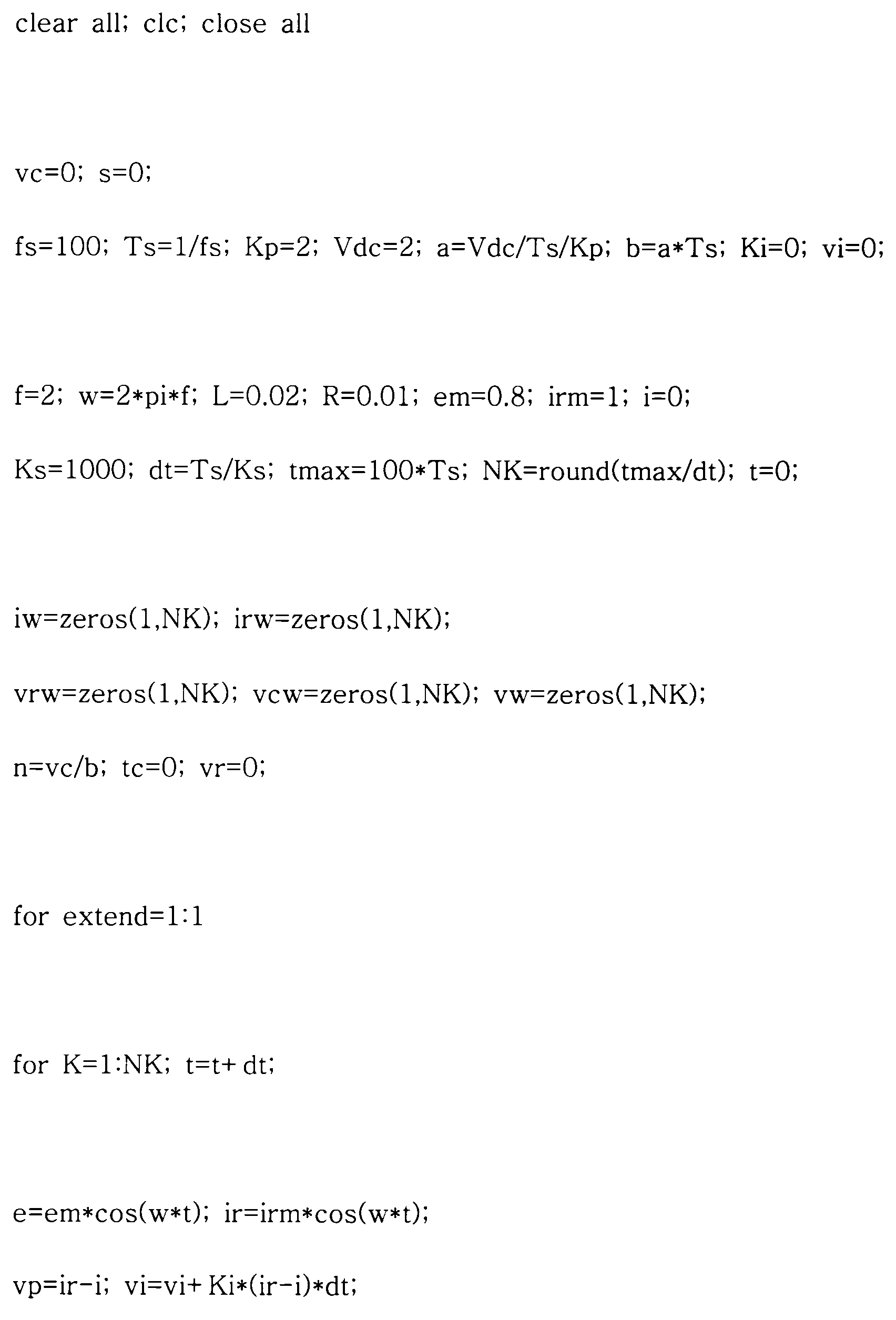
% Proportional - Integral Feedback
%% Sampling Proportion - Integral Feedback
% An embodiment of the preceding carrier pulse width modulation method

3A shows the modulation reference signal vr and the carrier signal vc of the preceding carrier pulse width modulation method in the case of DC-AC two-level proportional feedback current control, and FIG. 3B shows the output voltage v according to FIG. And Fig. 3C shows the reference current ir and output current i according to Fig. 3B. The preceding carrier pulse width modulation method has a limitation on the proportional gain (Kp). FIG. 3 shows a case where the proportional gain Kp is set to 2, which is the maximum. When the proportional gain (Kp) is larger, multiple intersections occur. In most cases, the transient response speed or steady-state error is not satisfactory even if the proportional gain (Kp) is maximized in the preceding carrier pulse width modulation method.
FIG. 4 shows a preceding carrier pulse width modulation method in the case of DC-AC 2-level proportional-integral feedback current control. The preceding carrier pulse width modulation method also has a limit on the integral gain (Ki). FIG. 4 shows a case where the integration gain Ki is set to 50, which is the maximum, with the proportional gain Kp set to 2. When the integral gain (Ki) becomes larger, multiple intersections occur or become unstable. Most of the preceding carrier pulse width modulation methods can not sufficiently reduce the transient response speed or the steady state error even if the proportional gain (Kp) and the integration gain (Ki) are maximized.
FIG. 5 shows a preceding carrier pulse width modulation method in the case of DC-AC two-level sampled proportional feedback current control. Sampling at intervals of the switching period can suppress the switching ripple included in the modulation reference signal, but it does not help to increase the gain of the compensator. Because of the sampling delay, there is another limit to the proportional gain (Kp). FIG. 5 shows a case where the proportional gain Kp is set to 2, which is the maximum. When the proportional gain (Kp) becomes larger, vibration and divergence occur.
FIG. 6 shows a preceding carrier pulse width modulation method in the case of DC-AC 2-level sampling, proportional-integral feedback current control. The sampling delay also causes another limitation on the integral gain (Ki). FIG. 6 shows a case where the integration gain (Ki) is set to almost the maximum value of 50 with the proportional gain (Kp) set to 2. When the integral gain (Ki) becomes larger, vibration and divergence occur. As a result, even in the case of the sampling control of the interval of the switching cycle, the preceding carrier pulse width modulation method is often unable to sufficiently reduce the transient response speed or the steady state error.
If the proportional gain (Kp) and the integral gain (Ki) are limited, there is a burden to precisely tune the proportional gain (Kp) and the integral gain (Ki) so as not to exceed this limit. In addition, variations of various parameters and parameters of the system should be considered. If the proportional gain (Kp) and the integral gain (Ki) are limited, the adaptability can not be high, and reliability, universality, and convenience can not be high.
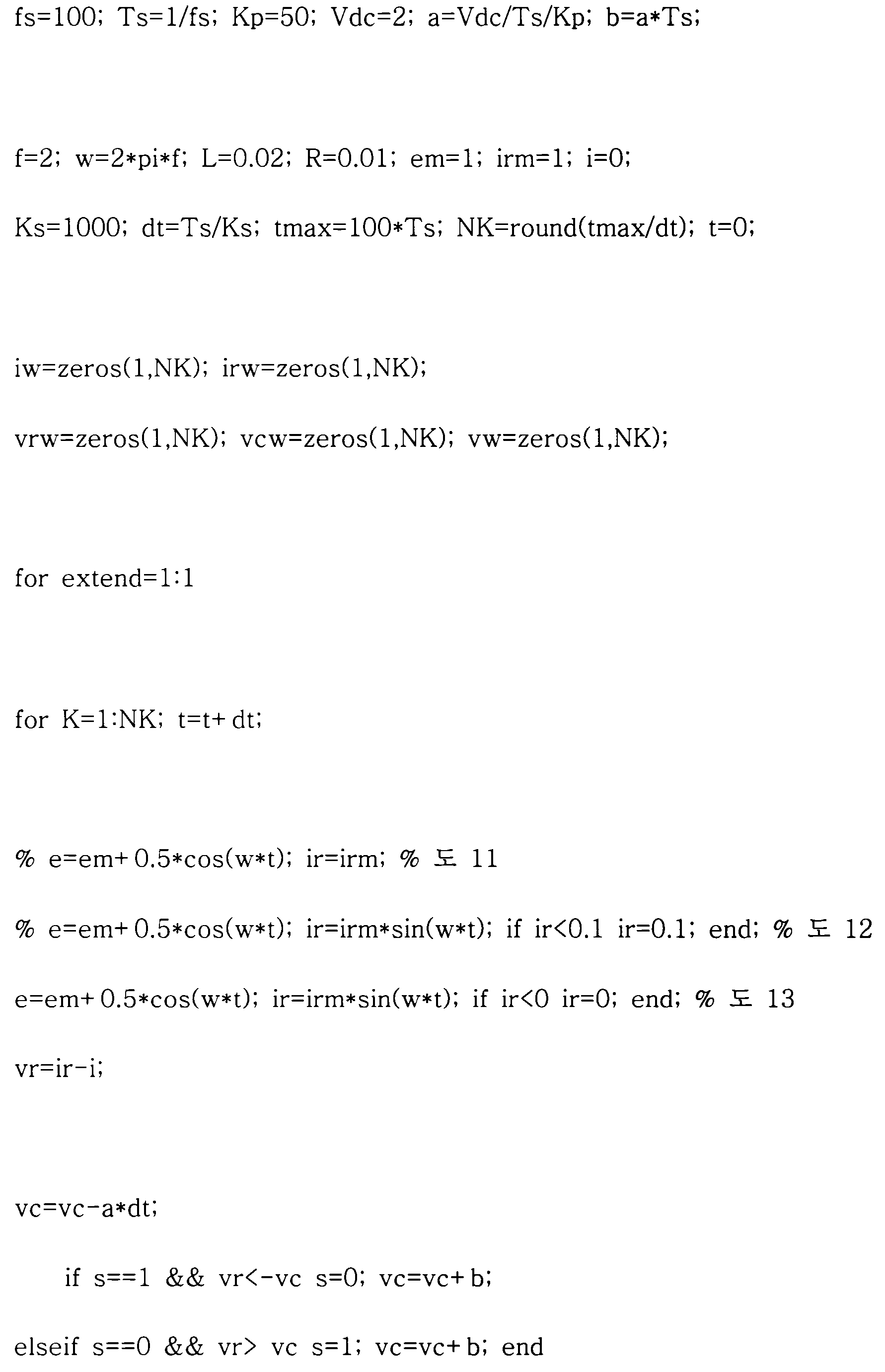
The following is a MATLAB program that describes an embodiment of the carrier pulse width modulation method of the present invention in the case of a DC-AC two-level closed loop. This is the case for a circuit in which inductance L, resistance R, and electromotive force e are connected in series to the output voltage terminals, proportional feedback current (i) control, and so on in all of the following programs.

% Embodiment of the Present Invention Carrier Pulse Width Modulation Method

%% Another embodiment of the carrier pulse width modulation method of the present invention

FIG. 7 shows a carrier pulse width modulation method of the present invention in the case of DC-AC two-level proportional feedback current control. FIG. 7 shows a case where the proportional gain (Kp) is 50, and shows excellent performance in both the transient response speed and the steady state error. The carrier signal vc appears as a kind of permissive band.
FIG. 8 shows a case where the proportional gain Kp is changed to 100 in the case of FIG. The larger the proportional gain (Kp), the more the transient response rate and the steady-state error are improved. The carrier signal vc becomes smaller in inclination and becomes entirely flat.
FIG. 9 shows a case where the inductance L is changed to 0.01 in the case of FIG. 8, and FIG. 10 shows a case where the inductance L is changed to 0.04 in the case of FIG. Even if the system parameters or parameters such as inductance fluctuate, the switching frequency becomes constant at steady state.
Meanwhile, another embodiment described in the program operates in the same manner as in the first embodiment when the reference switching number Ns is 1, and operates similarly when the reference switching number Ns is changed to 2 or more.
In the carrier pulse width modulation method of the present invention, the transient time for stabilizing the switching frequency is generated, and the transient time becomes longer as the proportional gain (Kp) is larger. However, as long as the proportional gain (Kp) is not very large, the transient time is short enough and it is also rare that the proportional gain (Kp) needs to be very large.
In the carrier pulse width modulation method of the present invention, other compensators such as a proportional-integral compensator may be employed, but in most cases, the proportional compensator alone exhibits a satisfactory performance. In the carrier pulse width modulation method of the present invention, there is no gain limit of the compensator, and the gain of the compensator can be increased as desired or necessary. Therefore, improvement effects can be obtained in almost all aspects such as transient response speed, tracking error and steady state error, adaptability to system fluctuation, and burden of fine tuning. Further, since there is no gain limit of the compensator, there is a large margin in the gain value, and therefore, the effect of improving reliability, versatility, and convenience can be obtained.
Carrier Pulse Width Modulation Method for DC-DC 2-Level Closed Loop
The following is a MATLAB program that describes an embodiment of the carrier pulse width modulation method of the present invention in the case of DC-DC two-level proportional feedback current control. Current is limited to a positive number.


11 shows an inventive carrier pulse width modulation method in the case of DC-DC two-level proportional feedback current control. Fig. 11 shows an intentionally large AC component included in the electromotive force e. Fig. 12 shows a case where there is a discontinuous current mode in the output current (i) in the case of Fig. FIG. 13 shows a case where the reference current ir is 0 in the case of FIG. When the proportional gain (Kp) is too large in the presence of the discontinuous current mode, the switching is not evenly distributed.
The following is a MATLAB program that describes an embodiment of the carrier pulse width modulation method of the present invention in the case of a power factor correction rectifier proportional feedback. In the program, the current flows backwards from the electromotive force (e) to the converter, and is limited to negative.


FIG. 14 shows a carrier pulse width modulation method of the present invention in the case of a power factor correcting rectifier proportional feedback.
Carrier Pulse Width Modulation Method for Multi-Level Closed Loop
The following is a MATLAB program that describes an embodiment of the carrier pulse width modulation method of the present invention in the case of a DC-AC multi-level proportional feedback current control.


FIG. 15 shows a carrier pulse width modulation method of the present invention in the case of DC-AC 5-level proportional feedback current control. The band margin (bm) can be either zero or a small value.
Carrier Pulse Width Modulation Method for Two-Phase Closed Loop
The following is a MATLAB program that describes the first embodiment of the inventive carrier pulse width modulation method for a DC-AC two-phase proportional feedback current control case. This embodiment is characterized in that a carrier wave is used for each of the two phases.


16 shows a first embodiment of a carrier pulse width modulation method of the present invention in the case of DC-AC two-phase proportional feedback current control.
The following is a MATLAB program that describes the second embodiment of the carrier pulse width modulation method of the present invention in the case of direct current-ac two-phase proportional feedback current control. This embodiment is characterized in that a two-phase common single carrier is used.

% Second embodiment

%% Modified embodiment

17 shows a second embodiment of a carrier pulse width modulation method of the present invention in the case of direct current-alternating two-phase proportional feedback current control. Comparing FIG. 17 with FIG. 16A, the form of the modulation reference signal vr is the same only in the shape of the carrier signal vc. That is, the second embodiment and the first embodiment operate in the same manner. On the other hand, the modified embodiment described in the program operates similarly.
The following is a MATLAB program that describes the third embodiment of the carrier pulse width modulation method of the present invention in the case of a DC-AC two-phase proportional feedback current control. This embodiment is characterized by using the carrier pulse width modulation method of the present invention in the case of DC-AC three-level.

% Example 3

%% Modified embodiment

The third embodiment operates in the same manner as the second embodiment. On the other hand, the modified embodiment described in the program operates similarly.
Carrier Pulse Width Modulation Method for Polyphase Closed Loop
The following is a MATLAB program that describes the first embodiment of the carrier pulse width modulation method of the present invention in the case of DC-AC neutral point connection polyphase proportional feedback current control. This embodiment is characterized in that a carrier wave is used for each of the polyphase. In the program, the load is a multiphase specific gravity multiple winding permanent magnet non - dipole constant speed synchronous motor model.

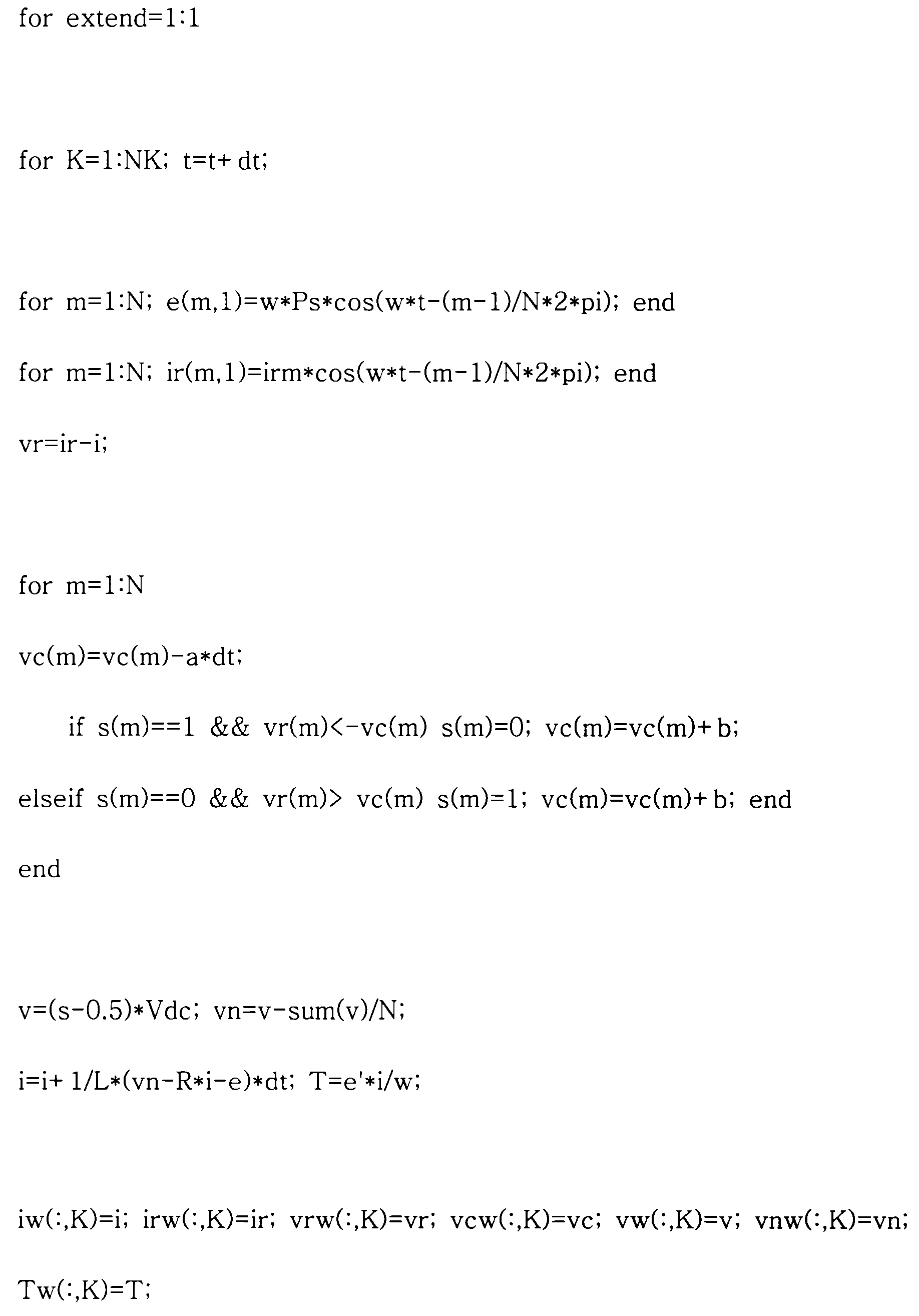

18 shows a first embodiment of a carrier pulse width modulation method of the present invention in the case of DC-AC neutral point connection three-phase proportional feedback current control. 18a shows the modulation reference signal vr and the carrier signal vc of the first phase, Fig. 18b shows the DC side neutral phase reference phase voltage v on the first phase, Fig. 18c shows the AC side neutral phase reference phase voltage vn 18d shows the reference current ir and the output current i of the first phase, and Fig. 18e shows the generated torque T. Fig.
The present invention carrier pulse width modulation method in the case of DC-AC neutral point connection polyphase proportional feedback current control operates similarly to the preceding hysteresis pulse width modulation method without the polyphase being synchronized when the proportional gain (Kp) is too large. When the proportional gain Kp is very large, the inductance L is too small, or the rotation speed is too slow, the phenomenon that the polyphase is undesirably synchronized may occur. Therefore, unfortunately, the carrier pulse width modulation method of the present invention in the case of DC-AC neutral point connection polyphase proportional feedback current control needs to suitably tune the proportional gain Kp.
The following is a MATLAB program that describes the second embodiment of the inventive carrier pulse width modulation method for a DC-AC multiphase proportional feedback current control case. This embodiment is characterized by using a polyphase common single carrier.


19 shows a second embodiment of the carrier pulse width modulation method of the present invention in the case of direct current-ac three-phase proportional feedback current control. 19 shows the modulation reference signal vr and the polyphase common single carrier signal vc on the first phase. Comparing FIG. 19 and FIG. 18A, only the shape of the carrier signal vc is different, and the shape of the modulation reference signal vr is almost the same. That is, the second embodiment and the first embodiment operate substantially the same.
A carrier pulse width modulation method for closed loop control of a power converter, the method comprising: receiving a modulation reference signal as an input and outputting a control signal of the power converter as an output; Providing a carrier signal; Setting a slope and a step value of the carrier signal; Decreasing the carrier signal to the slope according to time; And switching the control signal by comparing the modulation reference signal and the carrier signal, and adding the step value to the carrier signal, and a wide variety of implementations and modifications are possible. While important or preferred embodiments and modifications thereof have been described in the examples, it is not uncommon for all embodiments and variations to be described in this specification and claims. For example, the present invention may be implemented in an analog manner or in a digital manner. Also, for example, the slope and the step value are preferably constant in most applications, but may be non-linear or variable for the purpose of limiting the size of the switching ripple or dispersing the frequency spectrum of the switching ripple. Any implementation or variation having the main features of the invention is desired to be understood as an equivalent of the present invention.
Claims (5)
Providing a carrier signal;
Setting a slope and a step value of the carrier signal;
Decreasing the carrier signal to the slope according to time; And
Switching the control signal by comparing the modulation reference signal and the carrier signal, and adding the step value to the carrier signal;
And modulating the modulated carrier signal by a carrier wave.
Providing a carrier signal vc;
Setting a slope (a) and a step value (b) of the carrier signal (vc);
Decreasing the carrier signal vc to the slope a according to time; And
The control signal s is changed to a low level (0) when the control signal s is at a high level 1 and the modulation reference signal vr is smaller than a negative value of the carrier signal vc, Adding the step value (b) to the carrier signal (vc); Otherwise, when the control signal s is at a low level (0) and the modulation reference signal vr is greater than the carrier signal vc, the control signal s is changed to a high level (1) Adding the step value b to the signal vc;
And modulating the modulated carrier signal by a carrier wave.
Providing a carrier signal vc;
Setting a slope (a), a step value (b), and a band margin (bm) of the carrier signal (vc);
Decreasing the carrier signal vc to the slope a according to time;
The control signal s is changed to a low level (0) when the control signal s is at a high level 1 and the modulation reference signal vr is smaller than a negative value of the carrier signal vc, Adding the step value (b) to the carrier signal (vc); Otherwise, when the control signal s is at a low level (0) and the modulation reference signal vr is greater than the carrier signal vc, the control signal s is changed to a high level (1) Adding the step value b to the signal vc;
When the control signal s is at a high level 1 and the modulation reference signal vr is greater than the band margin bm plus the carrier signal vc, Changing to a level; And
When the control signal s is at a low level and the modulation reference signal vr is smaller than a value obtained by subtracting the band margin bm from a negative value of the carrier signal vc, ss) to the lower level;
And modulating the modulated carrier signal by a carrier wave.
Providing a carrier signal vc for each phase m;
Setting a slope (a) and a step value (b) of the carrier signal (vc);
For each phase (m), decreasing the carrier signal (vc) to the slope (a) with respect to time; And
When the control signal s is at a high level 1 and the modulation reference signal vr is smaller than the negative value of the carrier signal vc for each phase m, To the low level (0) and adds the step value (b) to the carrier signal (vc); Otherwise, when the control signal s is at a low level (0) and the modulation reference signal vr is greater than the carrier signal vc, the control signal s is changed to a high level (1) Adding the step value b to the signal vc;
And modulating the modulated carrier signal by a carrier wave.
Providing a carrier signal vc and an auxiliary control signal sa;
Setting a slope (a) and a step value (b) of the carrier signal (vc);
Decreasing the carrier signal vc to the slope a according to time;
(1), the control signal (s) is at a high level (1) and the modulation reference signal (vr) is at a high level (1) The control signal (s) is changed to a low level (0) when it is smaller than a negative value; Otherwise, when the auxiliary control signal sa is at a low level 0 and the control signal s is at a low level 0 and the modulation reference signal vr is greater than the carrier signal vc, (s) to high level (1); And
The step value b is added to the carrier signal vc when the auxiliary control signal sa is at a high level 1 and the control signal s of all phases is at a low level 0, Changes the signal sa to a low level (0); The step value b is added to the carrier signal vc when the auxiliary control signal sa is at a low level 0 and the control signal s of all phases is at a high level 1, Changing the signal sa to a high level (1);
And modulating the modulated carrier signal by a carrier wave.
Priority Applications (2)
| Application Number | Priority Date | Filing Date | Title |
|---|---|---|---|
| KR1020130049853A KR20140131040A (en) | 2013-05-03 | 2013-05-03 | Carrier pulse width modulation method |
| PCT/KR2014/003901 WO2014178673A1 (en) | 2013-05-03 | 2014-05-01 | Pulse width modulation method for controlling power converter |
Applications Claiming Priority (1)
| Application Number | Priority Date | Filing Date | Title |
|---|---|---|---|
| KR1020130049853A KR20140131040A (en) | 2013-05-03 | 2013-05-03 | Carrier pulse width modulation method |
Publications (1)
| Publication Number | Publication Date |
|---|---|
| KR20140131040A true KR20140131040A (en) | 2014-11-12 |
Family
ID=52452621
Family Applications (1)
| Application Number | Title | Priority Date | Filing Date |
|---|---|---|---|
| KR1020130049853A KR20140131040A (en) | 2013-05-03 | 2013-05-03 | Carrier pulse width modulation method |
Country Status (1)
| Country | Link |
|---|---|
| KR (1) | KR20140131040A (en) |
-
2013
- 2013-05-03 KR KR1020130049853A patent/KR20140131040A/en not_active Application Discontinuation
Similar Documents
| Publication | Publication Date | Title |
|---|---|---|
| US10224830B2 (en) | System and method for controlling a back-to-back three-level converter with voltage ripple compensation | |
| KR102009509B1 (en) | Apparatus and method for generating offset voltage of 3-phase inverter | |
| AU2012382463B2 (en) | Apparatus and method for providing uninterruptible power | |
| US9871462B2 (en) | Regenerative variable frequency drive with auxiliary power supply | |
| KR102009512B1 (en) | Apparatus and method for generating offset voltage of 3-phase inverter | |
| Maswood et al. | Average and hysteresis current-controlled three-phase three-level unity power factor rectifier operation and performance | |
| Husev et al. | Single phase three-level quasi-z-source inverter with a new boost modulation technique | |
| AU2015417472A1 (en) | Welding power supply with extended voltage characteristic | |
| JP4929863B2 (en) | Power converter | |
| US9190929B2 (en) | Multi-level rectifiers | |
| US20230074022A1 (en) | Power converter topologies with power factor correction circuits controlled using adjustable deadtime | |
| KR102016741B1 (en) | Sinlge-phase npc 3-level pwm converter for high-speed railway propulsion system using discontinuous modulation and method of controlling the same | |
| Schellekens et al. | Elimination of zero-crossing distortion for high-precision amplifiers | |
| Vodovozov et al. | Power electronic converters | |
| JP6968361B2 (en) | Power conversion circuit and its control method | |
| US20230076369A1 (en) | Unidirectional power converters with power factor correction circuits controlled using adjustable deadtime | |
| CN112787522B (en) | Linear and nonlinear dynamic bus control for active front-end applications | |
| RAJ et al. | Comparative analysis of single phase bridgeless buck rectifier and single phase multilevel buck rectifier | |
| KR102226290B1 (en) | ACDC Converter | |
| KR20140131040A (en) | Carrier pulse width modulation method | |
| Suzdalenko et al. | Transitional Average Current Sensorless Control during Peak-to-Peak Value Changes | |
| KR20140131039A (en) | Hysteresis pulse width modulation method | |
| Farhadi et al. | Predictive control of neutral-point clamped indirect matrix converter | |
| Karunakar et al. | Dynamic analysis of three phase Z-source boost-buck rectifier | |
| Brando et al. | A novel inductor based balancing circuit for diode clamped converters |
Legal Events
| Date | Code | Title | Description |
|---|---|---|---|
| WITN | Withdrawal due to no request for examination |