KR20140128355A - Apparatus, hybrid laminated body, method, and materials for temporary substrate support - Google Patents
Apparatus, hybrid laminated body, method, and materials for temporary substrate support Download PDFInfo
- Publication number
- KR20140128355A KR20140128355A KR20147023802A KR20147023802A KR20140128355A KR 20140128355 A KR20140128355 A KR 20140128355A KR 20147023802 A KR20147023802 A KR 20147023802A KR 20147023802 A KR20147023802 A KR 20147023802A KR 20140128355 A KR20140128355 A KR 20140128355A
- Authority
- KR
- South Korea
- Prior art keywords
- layer
- substrate
- coating
- support
- light
- Prior art date
Links
Images


Classifications
-
- B—PERFORMING OPERATIONS; TRANSPORTING
- B32—LAYERED PRODUCTS
- B32B—LAYERED PRODUCTS, i.e. PRODUCTS BUILT-UP OF STRATA OF FLAT OR NON-FLAT, e.g. CELLULAR OR HONEYCOMB, FORM
- B32B38/00—Ancillary operations in connection with laminating processes
- B32B38/10—Removing layers, or parts of layers, mechanically or chemically
-
- H—ELECTRICITY
- H01—ELECTRIC ELEMENTS
- H01L—SEMICONDUCTOR DEVICES NOT COVERED BY CLASS H10
- H01L21/00—Processes or apparatus adapted for the manufacture or treatment of semiconductor or solid state devices or of parts thereof
- H01L21/67—Apparatus specially adapted for handling semiconductor or electric solid state devices during manufacture or treatment thereof; Apparatus specially adapted for handling wafers during manufacture or treatment of semiconductor or electric solid state devices or components ; Apparatus not specifically provided for elsewhere
- H01L21/683—Apparatus specially adapted for handling semiconductor or electric solid state devices during manufacture or treatment thereof; Apparatus specially adapted for handling wafers during manufacture or treatment of semiconductor or electric solid state devices or components ; Apparatus not specifically provided for elsewhere for supporting or gripping
- H01L21/6835—Apparatus specially adapted for handling semiconductor or electric solid state devices during manufacture or treatment thereof; Apparatus specially adapted for handling wafers during manufacture or treatment of semiconductor or electric solid state devices or components ; Apparatus not specifically provided for elsewhere for supporting or gripping using temporarily an auxiliary support
-
- B—PERFORMING OPERATIONS; TRANSPORTING
- B32—LAYERED PRODUCTS
- B32B—LAYERED PRODUCTS, i.e. PRODUCTS BUILT-UP OF STRATA OF FLAT OR NON-FLAT, e.g. CELLULAR OR HONEYCOMB, FORM
- B32B37/00—Methods or apparatus for laminating, e.g. by curing or by ultrasonic bonding
- B32B37/14—Methods or apparatus for laminating, e.g. by curing or by ultrasonic bonding characterised by the properties of the layers
- B32B37/24—Methods or apparatus for laminating, e.g. by curing or by ultrasonic bonding characterised by the properties of the layers with at least one layer not being coherent before laminating, e.g. made up from granular material sprinkled onto a substrate
- B32B2037/243—Coating
-
- B—PERFORMING OPERATIONS; TRANSPORTING
- B32—LAYERED PRODUCTS
- B32B—LAYERED PRODUCTS, i.e. PRODUCTS BUILT-UP OF STRATA OF FLAT OR NON-FLAT, e.g. CELLULAR OR HONEYCOMB, FORM
- B32B2457/00—Electrical equipment
- B32B2457/14—Semiconductor wafers
-
- B—PERFORMING OPERATIONS; TRANSPORTING
- B32—LAYERED PRODUCTS
- B32B—LAYERED PRODUCTS, i.e. PRODUCTS BUILT-UP OF STRATA OF FLAT OR NON-FLAT, e.g. CELLULAR OR HONEYCOMB, FORM
- B32B33/00—Layered products characterised by particular properties or particular surface features, e.g. particular surface coatings; Layered products designed for particular purposes not covered by another single class
-
- B—PERFORMING OPERATIONS; TRANSPORTING
- B32—LAYERED PRODUCTS
- B32B—LAYERED PRODUCTS, i.e. PRODUCTS BUILT-UP OF STRATA OF FLAT OR NON-FLAT, e.g. CELLULAR OR HONEYCOMB, FORM
- B32B37/00—Methods or apparatus for laminating, e.g. by curing or by ultrasonic bonding
- B32B37/12—Methods or apparatus for laminating, e.g. by curing or by ultrasonic bonding characterised by using adhesives
-
- B—PERFORMING OPERATIONS; TRANSPORTING
- B32—LAYERED PRODUCTS
- B32B—LAYERED PRODUCTS, i.e. PRODUCTS BUILT-UP OF STRATA OF FLAT OR NON-FLAT, e.g. CELLULAR OR HONEYCOMB, FORM
- B32B37/00—Methods or apparatus for laminating, e.g. by curing or by ultrasonic bonding
- B32B37/14—Methods or apparatus for laminating, e.g. by curing or by ultrasonic bonding characterised by the properties of the layers
- B32B37/24—Methods or apparatus for laminating, e.g. by curing or by ultrasonic bonding characterised by the properties of the layers with at least one layer not being coherent before laminating, e.g. made up from granular material sprinkled onto a substrate
-
- B—PERFORMING OPERATIONS; TRANSPORTING
- B32—LAYERED PRODUCTS
- B32B—LAYERED PRODUCTS, i.e. PRODUCTS BUILT-UP OF STRATA OF FLAT OR NON-FLAT, e.g. CELLULAR OR HONEYCOMB, FORM
- B32B43/00—Operations specially adapted for layered products and not otherwise provided for, e.g. repairing; Apparatus therefor
- B32B43/006—Delaminating
-
- H—ELECTRICITY
- H01—ELECTRIC ELEMENTS
- H01L—SEMICONDUCTOR DEVICES NOT COVERED BY CLASS H10
- H01L21/00—Processes or apparatus adapted for the manufacture or treatment of semiconductor or solid state devices or of parts thereof
- H01L21/67—Apparatus specially adapted for handling semiconductor or electric solid state devices during manufacture or treatment thereof; Apparatus specially adapted for handling wafers during manufacture or treatment of semiconductor or electric solid state devices or components ; Apparatus not specifically provided for elsewhere
- H01L21/67005—Apparatus not specifically provided for elsewhere
- H01L21/67011—Apparatus for manufacture or treatment
- H01L21/67092—Apparatus for mechanical treatment
-
- H—ELECTRICITY
- H01—ELECTRIC ELEMENTS
- H01L—SEMICONDUCTOR DEVICES NOT COVERED BY CLASS H10
- H01L21/00—Processes or apparatus adapted for the manufacture or treatment of semiconductor or solid state devices or of parts thereof
- H01L21/67—Apparatus specially adapted for handling semiconductor or electric solid state devices during manufacture or treatment thereof; Apparatus specially adapted for handling wafers during manufacture or treatment of semiconductor or electric solid state devices or components ; Apparatus not specifically provided for elsewhere
- H01L21/673—Apparatus specially adapted for handling semiconductor or electric solid state devices during manufacture or treatment thereof; Apparatus specially adapted for handling wafers during manufacture or treatment of semiconductor or electric solid state devices or components ; Apparatus not specifically provided for elsewhere using specially adapted carriers or holders; Fixing the workpieces on such carriers or holders
-
- H—ELECTRICITY
- H01—ELECTRIC ELEMENTS
- H01L—SEMICONDUCTOR DEVICES NOT COVERED BY CLASS H10
- H01L21/00—Processes or apparatus adapted for the manufacture or treatment of semiconductor or solid state devices or of parts thereof
- H01L21/67—Apparatus specially adapted for handling semiconductor or electric solid state devices during manufacture or treatment thereof; Apparatus specially adapted for handling wafers during manufacture or treatment of semiconductor or electric solid state devices or components ; Apparatus not specifically provided for elsewhere
- H01L21/683—Apparatus specially adapted for handling semiconductor or electric solid state devices during manufacture or treatment thereof; Apparatus specially adapted for handling wafers during manufacture or treatment of semiconductor or electric solid state devices or components ; Apparatus not specifically provided for elsewhere for supporting or gripping
- H01L21/6835—Apparatus specially adapted for handling semiconductor or electric solid state devices during manufacture or treatment thereof; Apparatus specially adapted for handling wafers during manufacture or treatment of semiconductor or electric solid state devices or components ; Apparatus not specifically provided for elsewhere for supporting or gripping using temporarily an auxiliary support
- H01L21/6836—Wafer tapes, e.g. grinding or dicing support tapes
-
- H—ELECTRICITY
- H01—ELECTRIC ELEMENTS
- H01L—SEMICONDUCTOR DEVICES NOT COVERED BY CLASS H10
- H01L2221/00—Processes or apparatus adapted for the manufacture or treatment of semiconductor or solid state devices or of parts thereof covered by H01L21/00
- H01L2221/67—Apparatus for handling semiconductor or electric solid state devices during manufacture or treatment thereof; Apparatus for handling wafers during manufacture or treatment of semiconductor or electric solid state devices or components; Apparatus not specifically provided for elsewhere
- H01L2221/683—Apparatus for handling semiconductor or electric solid state devices during manufacture or treatment thereof; Apparatus for handling wafers during manufacture or treatment of semiconductor or electric solid state devices or components; Apparatus not specifically provided for elsewhere for supporting or gripping
- H01L2221/68304—Apparatus for handling semiconductor or electric solid state devices during manufacture or treatment thereof; Apparatus for handling wafers during manufacture or treatment of semiconductor or electric solid state devices or components; Apparatus not specifically provided for elsewhere for supporting or gripping using temporarily an auxiliary support
- H01L2221/68318—Auxiliary support including means facilitating the separation of a device or wafer from the auxiliary support
-
- H—ELECTRICITY
- H01—ELECTRIC ELEMENTS
- H01L—SEMICONDUCTOR DEVICES NOT COVERED BY CLASS H10
- H01L2221/00—Processes or apparatus adapted for the manufacture or treatment of semiconductor or solid state devices or of parts thereof covered by H01L21/00
- H01L2221/67—Apparatus for handling semiconductor or electric solid state devices during manufacture or treatment thereof; Apparatus for handling wafers during manufacture or treatment of semiconductor or electric solid state devices or components; Apparatus not specifically provided for elsewhere
- H01L2221/683—Apparatus for handling semiconductor or electric solid state devices during manufacture or treatment thereof; Apparatus for handling wafers during manufacture or treatment of semiconductor or electric solid state devices or components; Apparatus not specifically provided for elsewhere for supporting or gripping
- H01L2221/68304—Apparatus for handling semiconductor or electric solid state devices during manufacture or treatment thereof; Apparatus for handling wafers during manufacture or treatment of semiconductor or electric solid state devices or components; Apparatus not specifically provided for elsewhere for supporting or gripping using temporarily an auxiliary support
- H01L2221/68327—Apparatus for handling semiconductor or electric solid state devices during manufacture or treatment thereof; Apparatus for handling wafers during manufacture or treatment of semiconductor or electric solid state devices or components; Apparatus not specifically provided for elsewhere for supporting or gripping using temporarily an auxiliary support used during dicing or grinding
-
- H—ELECTRICITY
- H01—ELECTRIC ELEMENTS
- H01L—SEMICONDUCTOR DEVICES NOT COVERED BY CLASS H10
- H01L2221/00—Processes or apparatus adapted for the manufacture or treatment of semiconductor or solid state devices or of parts thereof covered by H01L21/00
- H01L2221/67—Apparatus for handling semiconductor or electric solid state devices during manufacture or treatment thereof; Apparatus for handling wafers during manufacture or treatment of semiconductor or electric solid state devices or components; Apparatus not specifically provided for elsewhere
- H01L2221/683—Apparatus for handling semiconductor or electric solid state devices during manufacture or treatment thereof; Apparatus for handling wafers during manufacture or treatment of semiconductor or electric solid state devices or components; Apparatus not specifically provided for elsewhere for supporting or gripping
- H01L2221/68304—Apparatus for handling semiconductor or electric solid state devices during manufacture or treatment thereof; Apparatus for handling wafers during manufacture or treatment of semiconductor or electric solid state devices or components; Apparatus not specifically provided for elsewhere for supporting or gripping using temporarily an auxiliary support
- H01L2221/6834—Apparatus for handling semiconductor or electric solid state devices during manufacture or treatment thereof; Apparatus for handling wafers during manufacture or treatment of semiconductor or electric solid state devices or components; Apparatus not specifically provided for elsewhere for supporting or gripping using temporarily an auxiliary support used to protect an active side of a device or wafer
-
- H—ELECTRICITY
- H01—ELECTRIC ELEMENTS
- H01L—SEMICONDUCTOR DEVICES NOT COVERED BY CLASS H10
- H01L2221/00—Processes or apparatus adapted for the manufacture or treatment of semiconductor or solid state devices or of parts thereof covered by H01L21/00
- H01L2221/67—Apparatus for handling semiconductor or electric solid state devices during manufacture or treatment thereof; Apparatus for handling wafers during manufacture or treatment of semiconductor or electric solid state devices or components; Apparatus not specifically provided for elsewhere
- H01L2221/683—Apparatus for handling semiconductor or electric solid state devices during manufacture or treatment thereof; Apparatus for handling wafers during manufacture or treatment of semiconductor or electric solid state devices or components; Apparatus not specifically provided for elsewhere for supporting or gripping
- H01L2221/68304—Apparatus for handling semiconductor or electric solid state devices during manufacture or treatment thereof; Apparatus for handling wafers during manufacture or treatment of semiconductor or electric solid state devices or components; Apparatus not specifically provided for elsewhere for supporting or gripping using temporarily an auxiliary support
- H01L2221/68381—Details of chemical or physical process used for separating the auxiliary support from a device or wafer
-
- Y—GENERAL TAGGING OF NEW TECHNOLOGICAL DEVELOPMENTS; GENERAL TAGGING OF CROSS-SECTIONAL TECHNOLOGIES SPANNING OVER SEVERAL SECTIONS OF THE IPC; TECHNICAL SUBJECTS COVERED BY FORMER USPC CROSS-REFERENCE ART COLLECTIONS [XRACs] AND DIGESTS
- Y10—TECHNICAL SUBJECTS COVERED BY FORMER USPC
- Y10T—TECHNICAL SUBJECTS COVERED BY FORMER US CLASSIFICATION
- Y10T156/00—Adhesive bonding and miscellaneous chemical manufacture
- Y10T156/10—Methods of surface bonding and/or assembly therefor
-
- Y—GENERAL TAGGING OF NEW TECHNOLOGICAL DEVELOPMENTS; GENERAL TAGGING OF CROSS-SECTIONAL TECHNOLOGIES SPANNING OVER SEVERAL SECTIONS OF THE IPC; TECHNICAL SUBJECTS COVERED BY FORMER USPC CROSS-REFERENCE ART COLLECTIONS [XRACs] AND DIGESTS
- Y10—TECHNICAL SUBJECTS COVERED BY FORMER USPC
- Y10T—TECHNICAL SUBJECTS COVERED BY FORMER US CLASSIFICATION
- Y10T428/00—Stock material or miscellaneous articles
- Y10T428/28—Web or sheet containing structurally defined element or component and having an adhesive outermost layer
- Y10T428/2839—Web or sheet containing structurally defined element or component and having an adhesive outermost layer with release or antistick coating
Abstract
투광 지지체, 투광 지지체 상에 배치된 잠재성 이형층, 잠재성 이형층 상에 배치된 결합층, 및 결합층 상에 배치된 열가소성 프라이밍 층을 포함하는 하이브리드 적층체가 제공된다. 하이브리드 적층체는 예를 들어, 연삭될 규소 웨이퍼와 같이 처리될 기판을 추가로 포함할 수 있다. 또한, 제공된 적층체를 제조하기 위한 방법이 제공된다.There is provided a hybrid laminate comprising a light-transmitting support, a latent releasing layer disposed on the light-transmitting support, a bonding layer disposed on the latent-releasing layer, and a thermoplastic priming layer disposed on the bonding layer. The hybrid laminate may further comprise a substrate to be treated, such as, for example, a silicon wafer to be ground. Also provided is a method for making a provided laminate.
Description
본 발명은 처리 중의 임시 기판 지지체에 관한 것이다.The present invention relates to a temporary substrate support during processing.
다양한 분야에서, 기판을 지지체에 임시 고정하는 것이 가능하거나 또는 처리를 향상시킬 수 있다. 예로서, 기판의 두께 감소는 종종 중요하다. 특히, 반도체 산업에서, 칩 적층 기술에 의한 고밀도 제조 및 반도체 패키지의 두께 감소의 목적에 응하여, 반도체 웨이퍼의 두께를 추가로 감소시키기 위한 노력이 진행중이다. 두께 감소는 패턴-형성된 회로를 포함하는 표면 반대쪽 표면 상의 반도체 웨이퍼의 소위 이면 연삭에 의해 수행된다. 일반적으로, 웨이퍼의 이면 또는 표면을 연삭하고, 후방 연삭 보호 테이프만으로 웨이퍼를 보유하면서 이를 이송하는 종래 기술에서, 연삭된 웨이퍼의 평탄하지 않은 두께 또는 연삭 이후에 보호 테이프를 가진 웨이퍼의 왜곡 같은 문제 때문에, 실제로는 단지 약 150 마이크로미터(μm)의 두께까지만 두께 감소가 달성될 수 있다. 예를 들어, 일본 미심사 특개평 제6-302569호(코카이(Kokai))는 압력-감응 아크릴레이트 접착제 테이프를 통해 링-형상 프레임 상에 웨이퍼가 보유되고, 프레임 상에 보유된 이 웨이퍼의 후방 표면이 연삭되며, 웨이퍼가 다음 단계로 이송되는 방법을 개시하고 있다. 그러나, 이 방법은 전술한 비균일성 또는 왜곡의 문제점을 겪지 않고 달성될 수 있는 현재의 웨이퍼 두께 수준보다 현저한 진보를 아직 달성하지 못한다.In various fields, it is possible to temporarily fix the substrate to the support or to improve the process. As an example, the thickness reduction of the substrate is often important. Particularly in the semiconductor industry, efforts are being made to further reduce the thickness of semiconductor wafers in response to the purpose of high density fabrication by chip stacking techniques and reduction of thickness of semiconductor packages. Thickness reduction is performed by so-called backside grinding of a semiconductor wafer on the surface opposite the surface including the pattern-formed circuit. Generally, in the prior art that grinds the backside or surface of a wafer and transports it while retaining the wafer with only the rear grinding protective tape, the problem of the uneven thickness of the ground wafer or the problem of distortion of the wafer with protective tape after grinding , In practice a thickness reduction can only be achieved up to a thickness of only about 150 micrometers (μm). For example, Japanese Unexamined Patent Application No. Hei 6-302569 (Kokai) discloses a method for manufacturing a semiconductor device in which a wafer is held on a ring-shaped frame through a pressure-sensitive acrylate adhesive tape, The surface is ground, and the wafer is transferred to the next step. However, this method does not yet achieve a significant improvement over the current wafer thickness level that can be achieved without experiencing the aforementioned problems of non-uniformity or distortion.
아크릴 접착제를 통해 경질 지지체 상에 웨이퍼를 견고히 고정한 상태로, 웨이퍼의 후방 표면을 연삭하고, 이를 이송하는 방법도 또한 제안되었다. 이는 이러한 지지체를 사용하여 웨이퍼를 지지함으로써 후방 표면 연삭 및 이송 동안 웨이퍼의 파괴를 방지하는 경향이 있다. 이 방법에 따라서, 웨이퍼는 전술한 방법에 비해 보다 낮은 두께 수준으로 처리될 수 있으나, 박형 웨이퍼는 웨이퍼를 파손시키지 않고서는 이 지지체로부터 분리될 수 없으며, 따라서, 이 방법은 반도체 웨이퍼의 박화 방법으로서는 실질적으로 사용될 수 있다.A method of grinding the rear surface of the wafer and transferring the wafer with the acrylic adhesive fixedly mounted on the hard substrate is also proposed. This tends to prevent backside surface grinding and destruction of the wafer during transfer by supporting the wafer using such a support. According to this method, the wafer can be processed to a lower thickness level than the above-described method, but the thin wafer can not be detached from the support without breaking the wafer, and thus the method can be used as a method of thinning semiconductor wafers Can be practically used.
따라서, 예를 들어, 분리에 따른 문제점을 극복할 수 있고, 또한 처리 중에 웨이퍼에 우수한 지지체를 제공할 수 있는, 규소 웨이퍼의 이면 연삭과 같은 공정 중에 임시 기판 지지체를 위한 방법 및 재료에 대한 필요가 있다. 기판이 잔류물을 남기지 않고 처리 이후에 지지체로부터 쉽게 제거될 수 있도록 무기 또는 유기 코팅을 포함할 수 있는 임시 기판 지지체를 제공할 필요가 있다. 또한, 범프 또는 포스트와 같은 기판 표면 토포그래피 상에 불필요한 응력을 부여하지 않고 고출력 분리를 가능하게 하는 공정에 대한 필요가 있다.There is therefore a need for methods and materials for temporary substrate supports during processes such as, for example, back grinding of silicon wafers, which can overcome the problems associated with separation and which can provide an excellent support to the wafer during processing have. There is a need to provide a temporary substrate support that can include an inorganic or organic coating such that the substrate can be easily removed from the substrate after processing without leaving residue. There is also a need for a process that enables high output isolation without imparting undue stresses to substrate surface topography such as bumps or posts.
일 양태에서, 투광 지지체, 투광 지지체 상에 배치된 잠재성 이형층, 잠재성 이형층 상에 배치된 결합층, 및 결합층 상에 배치된 열가소성 프라이밍 층을 포함하는 적층체가 제공된다. 일부 실시 형태에서, 지지체는 유리를 포함할 수 있다. 일부 실시 형태에서, 잠재성 이형층은 레이저 또는 레이저 다이오드로부터의 것과 같은 화학 방사선에 노출 시에 활성화될 수 있는 광열 변환층을 포함할 수 있다. 일부 실시 형태에서, 광열 변환층은 예를 들어, 실리카와 같은 투명 충전제를 포함할 수 있다. 일부 실시 형태에서, 결합층은 아크릴일 수 있는 열경화성 접착제일 수 있다. 일부 실시 형태에서, 열가소성 프라이밍 층은 폴리아릴설폰을 포함할 수 있다. 제공된 적층체는 열가소성 프라이밍 층과 접촉하는 처리될 기판을 추가로 포함할 수 있다. 일부 실시 형태에서, 처리될 기판은 규소 웨이퍼를 포함할 수 있다.In one aspect, a laminate is provided that includes a light-transmitting support, a latent releasing layer disposed on the light-transmitting support, a bonding layer disposed on the latent-releasing layer, and a thermoplastic priming layer disposed on the bonding layer. In some embodiments, the support may comprise glass. In some embodiments, the latent release layer may comprise a photo-thermal conversion layer that can be activated upon exposure to actinic radiation, such as from a laser or a laser diode. In some embodiments, the photothermal conversion layer may comprise a transparent filler, such as, for example, silica. In some embodiments, the bonding layer may be a thermosetting adhesive that may be acrylic. In some embodiments, the thermoplastic priming layer may comprise polyarylsulfone. The provided laminate may further comprise a substrate to be treated in contact with the thermoplastic priming layer. In some embodiments, the substrate to be processed may comprise a silicon wafer.
또 다른 양태에서, 열가소성 프라이밍 층을 기판 상으로 코팅하는 단계, 선택적으로, 코팅이 용매를 포함하는 경우 열가소성 프라이밍 층을 건조시키는 단계, 열가소성 프라이밍 층 상으로 결합층을 코팅하는 단계, 선택적으로, 결합층을 경화시키는 단계, 투광 지지체 상에 잠재성 이형층을 코팅하는 단계, 및 투광 지지체를 결합층에 적층하는 단계를 포함하는 적층체를 제조하기 위한 방법이 제공된다. 열가소성 프라이밍 층 또는 결합층의 코팅은 스핀 코팅, 스프레이 코팅, 디프 코팅, 스크린 프린팅, 다이 코팅, 또는 나이프 코팅을 포함할 수 있다.In another embodiment, the method includes the steps of coating a thermoplastic priming layer onto a substrate, optionally, drying the thermoplastic priming layer when the coating comprises a solvent, coating the bonding layer onto the thermoplastic priming layer, A step of curing the layer, a step of coating the latent releasable layer on the light-transmitting substrate, and a step of laminating the light-transmitting substrate to the bonding layer. The coating of the thermoplastic priming layer or bonding layer may include spin coating, spray coating, dip coating, screen printing, die coating, or knife coating.
또 다른 양태에서, 적층체를 제조하기 위한 방법은 기판을 처리하는 단계, 광열 변환층을 분해하고 이에 따라 상기 기판과 상기 투광 지지체를 분리시키기 위하여 투광 지지체를 통하여 광열 변환층을 조사하는 단계, 상기 기판으로부터 결합층을 박리하는 단계, 및 기판으로부터 열가소성 프라이밍 층을 제거하는 단계를 추가로 포함한다. 열가소성 프라이밍 층은 용매로 열가소성 프라이밍 층을 세척함으로써 제거될 수 있다.In another aspect, a method for manufacturing a laminate includes the steps of treating a substrate, irradiating the photo-thermal conversion layer through a light-transmitting substrate to decompose the photo-thermal conversion layer and thereby separate the substrate from the light- Peeling the bonding layer from the substrate, and removing the thermoplastic priming layer from the substrate. The thermoplastic priming layer can be removed by washing the thermoplastic priming layer with a solvent.
본 개시에서:In this disclosure:
"화학 방사선"은 자외선, 가시광선 및 적외선을 포함하고 광화학 반응을 생성할 수 있는 임의의 전자자기 방사선을 지칭하며,"Actinic radiation" refers to any electromagnetic radiation capable of generating a photochemical reaction, including ultraviolet, visible, and infrared radiation,
"투광 지지체"는 이를 통하여 상당 양(광화학 반응을 유발하기에 충분한)의 화학 방사선이 투과되도록 허용할 수 있는 재료를 지칭하며,"Transparent support" refers to a material through which a substantial amount of radiation (sufficient to cause a photochemical reaction) is allowed to penetrate,
"잠재성 이형층"은 2개의 재료들을 서로 결합하지만 외부 자극에 노출 시에 하나 또는 다른 재료에 대한 접착성을 잃을 수 있는 층을 지칭하며,"Latent releasing layer" refers to a layer that bonds two materials together but can lose adhesion to one or other materials upon exposure to external stimuli,
"열가소성"은 가열된 때에 가역적으로 액체로 변화하고 냉각된 때에 매우 유리질의 상태로 동결되는 것을 지칭하며, 및"Thermoplastic" refers to reversibly changing to liquid upon heating and freezing to a very vitreous state upon cooling, and "
"열경화성의" 또는 "열경화성"은 비가역적으로 경화되는 중합체 재료를 지칭한다."Thermosetting" or "thermosetting" refers to a polymeric material that is irreversibly cured.
제공된 적층체 및 이를 제조하는 방법은 예를 들어, 규소 웨이퍼의 이면 연삭과 같은 작업 중에 기판 지지체에 대해 제공된다. 열가소성 프라이밍 층의 사용은 결합층의 제거를 위해 일정한 층을 제공하는 다양한 화학물질을 갖는 기판에 대해 지지체를 제공한다. 게다가, 제공된 적층체는 기판 상에 불필요한 응력을 부여하지 않고 고출력 분리를 가능하게 한다. 이는 기판이 박형 웨이퍼일 때 특히 중요하다.The provided laminate and the method for manufacturing the same are provided for the substrate support during operations such as, for example, back grinding of silicon wafers. The use of a thermoplastic priming layer provides a support for substrates having various chemicals that provide a constant layer for removal of the bonding layer. In addition, the provided laminate enables high-power separation without giving unnecessary stress on the substrate. This is particularly important when the substrate is a thin wafer.
상기 요약은 본 발명의 모든 구현의 각각의 개시된 실시 형태를 설명하기 위한 것이 아니다. 하기의 도면 및 상세한 설명의 간략한 설명은 도식적인 실시 형태를 더욱 구체적으로 예시한다.The above summary is not intended to describe each disclosed embodiment of every implementation of the invention. BRIEF DESCRIPTION OF THE DRAWINGS The following drawings and the brief description of the detailed description more particularly illustrate schematic embodiments.
<도 1>
도 1은 제공된 적층체의 실시 형태의 측면 단면도.
<도 2>
도 2는 제공된 적층체의 또 다른 실시 형태의 측면 단면도.
<도 3a 및 도 3b>
도 3a 및 도 3b는 본 발명에서 유용한 진공 접착 장치를 도시하는 단면도.
<도 4a, 4a', 4b, 4c, 4d, 및 4e>
도 4a, 4a', 4b, 4c, 4d, 및 4e는 결합층을 박리하고 지지체를 분리하는 단계를 도시하는 도면.
<도 5>
도 5는 레이저 빔 조사 단계에서 사용될 수 있는 적층체 고정 장치의 단면도.
<도 6a, 6b, 6c, 6d, 6e, 및 6f>
도 6a, 6b, 6c, 6d, 6e, 및 6f는 레이저 조사 장치의 사시도.
<도 7a 및 도 7b>
도 7a 및 도 7b는 웨이퍼 및 지지체를 분리하는 공정에서 사용된 픽-업의 도식적 도면.
<도 8>
도 8은 결합 층이 웨이퍼로부터 박리되는 방법을 도시하는 도식적인 도면.
(발명의 상세한 설명)
하기의 설명에서, 본 발명의 설명의 일부를 이루며 몇몇 구체적인 실시 형태가 예로서 도시되어 있는 일련의 첨부 도면을 참조한다. 본 발명의 범주 또는 사상으로부터 벗어남이 없이 다른 실시 형태가 고려되고 이루어질 수 있음을 이해하여야 한다. 따라서, 하기의 상세한 설명은 제한적인 의미로 취해져서는 안 된다.
달리 지시되지 않는 한, 명세서 및 특허청구범위에 사용되는 특징부 크기, 양 및 물리적 특성을 표현하는 모든 수치는 모든 경우 "약"이라는 용어에 의해 수식되는 것으로 이해되어야 한다. 따라서, 반대로 지시되지 않는한, 전술된 명세서 및 첨부된 특허청구범위에 기재된 수치 파라미터는 당업자가 본 명세서에 개시된 교시 내용을 이용하여 얻고자 하는 원하는 특성에 따라 변할 수 있는 근사치이다. 종점(end point)에 의한 수치 범위의 사용은 그 범위 내의 모든 수 (예를 들어, 1 내지 5는 1, 1.5, 2, 2.75, 3, 3.80, 4 및 5를 포함함) 및 그 범위 내의 임의의 범위를 포함한다.
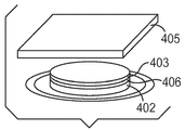
도 1은 제공된 적층체(laminated body, 100)의 실시 형태의 측면 단면도이다. 적층체(100)는 규소 웨이퍼 또는 반도체 웨이퍼인 연삭될 기판의 범프(bump, 104) 또는 솔더 볼(solder ball)을 포함할 수 있는 기판(102)을 포함한다. 열가소성 프라이밍 층(thermoplastic priming layer, 106)은 도 1에 도시된 바와 같이 솔더 범프(104)를 캡슐화할 수 있고 웨이퍼(102)의 회로 측(솔더 범프 측) 상에 배치된다. 결합층(108)은 열가소성 프라이밍 층(106)과 접촉하고, 열가소성 프라이밍 층(106)과 잠재성 이형층(110) 사이에 배치된다. 잠재성 이형층(110)은 투광 지지체(light-transmitting support, 112) 상에 배치된다.
도 2는 제공된 적층체(200)의 또 다른 실시 형태의 측면 단면도이다. 적층체(200)는 기판이 규소 웨이퍼 또는 반도체 웨이퍼인 경우 범프(204) 또는 솔더 볼을 포함할 수 있는 기판(202)을 포함한다. 열가소성 프라이밍 층(206)은 도 2에 도시된 바와 같이 솔더 범프(204)를 캡슐화할 수 있고 웨이퍼(202)의 회로 측(솔더 범프 측) 상에 배치된다. 결합층(208)은 열가소성 프라이밍 층(206)과 접촉하고, 열가소성 프라이밍 층(206)과 잠재성 이형층(210) 사이에 배치된다. 잠재성 이형층(210)은 투광 지지체(212) 상에 배치된다. 열가소성 에지 제거 영역(214)은 가용화 공정 화학물질로부터 보호되고 기판(202)의 에지에서 열가소성 프라이밍 층(206)을 제거하고 열 안정성 결합층(208)을 오버코팅함으로써 형성된다.
적층체는 투광 지지체를 포함한다. 투광 지지체는 레이저 또는 레이저 다이오드로부터의 것과 같이 화학 방사선 에너지를 투과시킬 수 있는 재료이다. 지지체의 투광도는 잠재성 이형층이 광-활성화되는 경우 잠재성 이형층의 분해를 가능하게 하기 위해 실용적 강도 수준의 방사선 에너지의 잠재성 이형층 내로의 투과를 방지하지 않는 한 제한되지 않는다. 그러나, 전형적으로 투과율은 예를 들어 50% 이상이다. 투광성 지지체는 전형적으로 충분히 높은 강성을 가지며, 지지체의 굴곡 강도는 전형적으로 2×10⁻³ (Paㆍ㎥) 이상, 보다 전형적으로는 3×10⁻² (Paㆍ㎥) 이상이다. 유용한 지지체의 예는 유리판 및 아크릴판을 포함한다. 또한, 잠재성 이형층과 같은 인접 층에 대한 접착 강도를 향상시키기 위해, 지지체는 필요 시, 실란 결합제, 등으로 표면 처리될 수 있다. UV-경화성 광열 변환층 또는 결합층을 사용하는 경우, 지지체는 전형적으로 자외선 방사선을 투과시킨다.
광열 변환층이 조사될 때, 잠재성 이형층이 광-활성화되는 경우 지지체는 잠재성 이형층 내에 발생된 열에 노출될 수 있다. 내열성, 내화학성 및 낮은 팽창 계수를 갖는 지지체가 제공된 적층체 내에서 사용될 수 있다. 이들 특성을 갖는 지지체 재료의 예는 파이렉스(Pyrex) 및 탬팩스(TeMpax)로서 입수가능한 붕규산 유리(borosilicate glass) 및 코닝 이글(Corning Eagle) XG와 같은 알칼리 토류 붕소-알루미노규산염 유리(alkaline earth boro-aluminosilicate glass)를 포함한다.
제공된 적층체는 투광 지지체 상에 배치된 잠재성 이형층을 포함한다. 잠재성 이형층은 외부 자극에 응답하여 접착성의 감소를 겪는 재료 또는 재료의 조합을 포함한다. 외부 자극은 가열 또는 냉각, 화학 방사선에 대한 노출, 스트레인, 습도, 산 또는 염기와 같은 화학 작용제에 대한 노출일 수 있다. 일 실시 형태에서, 잠재성 이형층은 적층체의 사용 온도 미만인 유리 전이 온도(Tg)를 갖는 열가소성 재료일 수 있다. 결합해제가 요구 시에, 적층체의 온도는 잠재성 이형 층이 접착성을 잃도록 야기하는 잠재성 이형 층의 Tg 미만으로 감소된다. 다른 실시 형태에서, 잠재성 이형층은 예를 들어, 미국 특허 제5,507,464호; 제6,162,534호; 제6,410,135호; 제6,541,089호; 및 제6,821,619호(모두가 헤머스키(Hamerski) 또는 헤머스키, 등)에 개시된 것과 같이 스트레인의 인가 시에 결합해제되는 재료를 포함할 수 있다. 일부 실시 형태에서, 잠재성 이형층은 예를 들어, 차례로 잠재성 이형층의 접착성을 감소시킬 수 있는 교차-결합을 개시할 수 있는 산 촉매와 같은 촉매를 생성하기 위해 화학 방사선 또는 열의 인가에 의해 교차결합될 수 있는 열가소성 재료일 수 있다. 예시적인 촉매는 광산-발생제, 잠재성 열 산 발생제, 또는 당업계에 잘 공지된 다른 잠재성 촉매를 포함할 수 있다. 일부 실시 형태에서, 잠재성 이형층은 광열 변환층일 수 있다.
광열 변환층은 흡광제 및 열 분해성 수지를 포함한다. 레이저 빔, 등의 형태로 광열 변환층에 인가되는 방사선 에너지는 흡광제에 의해 흡수되고, 열 에너지로 변환된다. 발생된 열 에너지는 광열 변환층의 온도를 급격히 상승시키고, 온도는 광열 변환층 내의 열 분해 수지(유기 성분)의 열 분해 온도에 도달하여 수지의 열 분해를 야기한다. 열 분해에 의해 발생된 가스는 광열 변환층 내에 공극층(공간 같은)을 형성하고, 광열 변환층을 두 부분으로 분할하는 것으로 믿어지며, 이에 따라 지지체와 적층체에 부착된 임의의 기판이 분리될 수 있다. 적합한 광열 변환층은 예를 들어, 미국 특허 제7,534,498호(노다(Noda) 등)에 기재된다.
흡광제는 사용되는 파장의 화학 방사선을 흡수할 수 있다. 방사선 에너지는 일반적으로 300 내지 11,000 나노미터(nm), 전형적으로는 300 내지 2,000 nm의 파장을 갖는 레이저 빔이며, 이의 구체적인 예는 1,064 nm의 파장으로 광을 방출하는 YAG 레이저, 532 nm의 파장의 제2 조화파 생성 YAG 레이저, 및, 780 내지 1,300 nm의 파장의 반도체 레이저를 포함한다. 비록, 흡광제가 레이저 빔의 파장에 의존하여 변하지만, 사용될 수 있는 흡광제의 예는 카본 블랙, 흑연 분말, 예컨대 철, 알루미늄, 구리, 니켈, 코발트, 망간, 크롬, 아연 및 텔루륨과 같은 마이크로입자 금속 분말, 예컨대 블랙 티타늄 산화물 같은 금속 산화물 분말 및 예컨대 방향성 디아미노-기반 금속 합성체(aromatic diamino-based metal complex), 지방족 디아민-기반 금속 합성체(aliphatic diamine-based metal complex), 방향족 디티올-기반 금속 합성체(aromatic dithiol-base metal complex), 메르캅토페놀-기반 금속 합성체(mercaptophenol-based metal complex), 스쿠아릴륨-기반 화합물(squarylium-based compound), 시아닌-기반 염료(acyanine-based dye), 메틴-기반 염료(methine-based dye), 나프토퀴논-기반 염료(naphthoquinone-based dye) 및 안트라퀴논-기반 염료(anthraquinone-based dye)와 같은 염료 및 안료를 포함한다. 흡광제는 기상 증착된 금속막을 포함하는 막의 형태일 수 있다. 이들 흡광제 중에서, 카본 블랙이 특히 유용하며, 그 이유는, 카본 블랙이 조사 이후 지지체로부터 기판을 분리시키기 위해 필요한 힘을 상당히 감소시키고, 분리를 가속하기 때문이다.
광열 변환층 내의 흡광제의 농도는 흡광제의 종류, 입자 상태(구조) 및 분산도에 따라 변하지만, 농도는 약 5 nm 내지 500 nm의 입자 크기를 갖는 일반적인 카본 블랙의 경우에, 일반적으로 5 부피% 내지 70 부피%이다. 농도가 5 부피% 미만인 경우, 광열 변환층의 열 발생이 열 분해성 수지의 분해에 불충분할 수 있으며, 70 부피%를 초과하는 경우, 광열 변환층의 성막 특성이 열악해지고, 다른 층에 대한 접합의 손상을 쉽게 유발할 수 있다. 결합층으로서 사용되는 접착제가 UV-경화성 접착제인 경우, 카본 블랙의 양이 과도하게 많으면, 접착제를 경화시키기 위한 자외선의 투과율이 감소한다. 따라서, 결합층으로서 UV-경화성 접착제를 사용하는 경우, 카본 블랙의 양은 60 부피% 이하여야 한다. 조사 이후 지지체의 제거 시의 힘을 감소시켜 연삭 동안의 광열 변환층의 마모(세척수 내의 연마제로 인한 마모 같은)를 방지하기 위해, 카본 블랙은 20 부피% 내지 60 부피%의 양으로, 보다 전형적으로는 35 부피% 내지 55 부피%의 양으로 광열 변환층 내에 포함된다.
사용될 수 있는 열 분해성 수지의 예는 젤라틴, 셀룰로오스, 셀룰로오스 에스테르(예를 들어, 셀룰로오스 아세테이트, 니트로셀룰로오스), 폴리페놀, 폴리비닐 부티랄, 폴리비닐 아세탈, 폴리카보네이트, 폴리우레탄, 폴리에스테르, 폴리오르소에스테르, 폴리아세탈, 폴리비닐 알콜, 폴리비닐피롤리돈, 비닐리덴 클로라이드와 아크릴로니트릴의 공중합체, 폴리(메트)아크릴레이트, 폴리비닐 클로라이드, 실리콘 수지 및 폴리우레탄 단위를 포함하는 블록 공중합체를 포함한다. 이들 수지는 개별적으로 또는 이의 둘 이상의 그 조합으로 사용될 수 있다. 수지의 유리 전이 온도(Tg)는 전형적으로 열 분해성 수지의 열 분해의 결과로서 공극층의 형성으로 인해 분리되고 나면 광열 변환층의 재접착을 방지하도록 실온(20℃) 이상이며, Tg는 더욱 전형적으로 재접착을 방지하도록 100℃이상이다. 투광성 지지체가 유리인 경우에, 유리와 광열 변환층 사이의 접착력을 증가시키기 위해, 유리 표면 상의 실라놀기(silanol group)에 수소-결합될 수 있는 극성기(예를 들어, -COOH, -OH)를 분자 내에 갖는 열 분해성 수지가 사용될 수 있다. 또한, 화학 에칭 같은 화학액 처리를 필요로 하는 응용에서, 광열 변환층에 내화학성을 부여하기 위해, 열처리 시에 자가-교차결합할 수 있는 기능기를 분자 내에 갖는 열 분해성 수지, 자외선 또는 가시광에 의해 교차결합할 수 있는 열 분해성 수지 또는 그의 전구체(예를 들어, 단량체 및/또는 올리고머의 혼합물)가 사용될 수 있다. 감압 접착제 광열 변환층으로서 광열 변환층을 형성하기 위해, 열 분해성 수지에 대해 사용될 수 있는 폴리(메트)아크릴레이트, 등으로부터 형성된 감압 접착제 중합체가 사용될 수 있다.
광열 변환층은 필요 시 투명 충전재(transparent filler)를 포함할 수 있다. 투명 충전재는 열 분해성 수지의 열 분해의 결과로서의 공극층의 형성으로 인해 분리되고 나면 광열 변환층의 재접착을 방지하도록 기능한다. 따라서, 기판의 연삭 및 후속 조사 이후, 기판과 지지체의 분리를 위해 필요한 힘이 추가로 감소될 수 있다. 또한, 재접착이 방지될 수 있기 때문에, 열 분해성 수지의 선택의 범위가 확장된다. 투명 충전재의 예는 실리카, 운모 및 바륨 황산염을 포함한다. 투명 충전재의 사용은 UV-경화성 접착제가 결합층으로서 사용될 때 특히 유리하다. 이는 현재 하기의 이유에 기인한 것으로 믿어진다. 카본 블랙 같은 입상 흡광제가 사용될 때, 흡광제는 분리를 위한 힘을 감소시키는 기능을 가지며, 또한, 자외선 광의 투과를 방해하도록 기능한다. 따라서, UV-경화성 접착제가 결합층으로서 사용될 때, 경화가 만족스럽게 진행되지 않거나, 매우 긴 시간을 필요로 할 수 있다. 이러한 경우에, 투명 충전재가 사용될 때, 기판 및 지지체는 UV-경화성 접착제의 경화를 방해하지 않고 조사 이후 쉽게 분리될 수 있다. 카본 블랙 같은 입상 흡광제가 사용될 때, 투명 충전재의 양은 흡광제의 총 양에 의해 결정될 수 있다. 광열 변환층 내의 투명 충전재 및 입상 흡광제(예를 들어, 카본 블랙)의 총 양은 전형적으로 광열 변환층의 부피에 기초하여 5 부피% 내지 70 부피%이다. 이 범위의 총 양에서, 기판과 지지체의 분리를 위한 힘이 충분히 감소될 수 있다. 그러나, 분리를 위한 힘은 또한 입상 흡광제 및 투명 충전재의 형상에 의해 영향을 받는다. 보다 구체적으로, 분리를 위한 힘은 거의 구형 같은 입자 형상이 비교적 단순한 경우 보다 입자 형상이 복잡한 경우(보다 복잡한 구조로부터 초래되는 입자 상태)에 때때로 작은 충전재 양으로 보다 효과적으로 감소된다.
입상 흡광제와 투명 충전재의 총 양은 일부 경우에 "최고 충전재 부피 농도"(TFVC; top filler volume concentration)에 기초하여 결정될 수 있다. 이는 입상 흡광제 및 투명 충전재의 혼합물이 건조 상태로 남아있고, 열 분해성 수지가 공극의 부피를 꼭 맞게 충전하는 양의 충전재와 혼합될 때의 충전재 부피 농도를 의미한다. 즉, 열 분해성 수지가 입상 흡광제와 투명 충전재의 혼합물 내의 공극의 부피를 꼭 맞게 충전하는 양의 충전재와 혼합될 때의 TFVC가 최고 충전재 부피 농도의 100%이다. 광열 변환층 내의 투명 충전재 및 입상 흡광제의 총 양은 전형적으로 최고 충전재 부피 농도의 80% 이상, 보다 전형적으로는 90% 이상이다. 추가 설명으로, 충전재(예를 들어, 카본 블랙 및 투명 충전재)의 총 부피 백분율은 "A"로 표시되고, 최고 충전재 부피 농도(TFVC)(충전재의 공극 부피를 충전하는 수지와의 충전재의 총 부피 백분율)는 "B"로 표시되며, 이때, A/B는 전형적으로 약 80%를 초과한다(보다 전형적으로는 A/B > 90%).
어떠한 이론으로도 구애받지 않을지라도, 현재로서는 광열 변환층 내의 흡광제(예를 들어, 카본 블랙)는 투명 지지체를 통해 조사되는 레이저 에너지를 흡수하고, 이를 열로 변환하며, 이 열이 매트릭스-수지를 분해하고, 가스 또는 공극을 생성하는 것으로 여겨진다. 결과적으로, 공극은 이 층을 2개의 층 같은 부분으로 분리하며, 그후, 반도체 웨이퍼가 지지체로부터 결합해제된다. 공극에 의해 분리된 표면은 소정 시간에 표면을 재접촉할 수 있다. 표면은 카본 블랙 입자 뿐만 아니라 잔류 수지를 가지며, 이 수지는 열 분해에 의해 분자량이 감소되어 있다. 재접촉(예를 들어, 재접착) 시에, 이 잔류 수지는 접착을 증가시킬 수 있다. 한편, 광열 변환층 뿐만 아니라, 접착제 층도 연성일 때, 재접촉 면적은 비교적 클 수 있으며, 이는 접착을 보다 커지게 하며, 손상 또는 파손 없이 지지체로부터 초박형 웨이퍼를 결합해제시키는 것을 매우 곤란하게 한다. 본 발명에서, A/B > 80%, 전형적으로는 A/B > 90%로 설정함으로써, 결합해제면 상의 잔류 수지가 감소된다. 그에 의해, 재접촉에 의해 생성되는 접착이 최소화될 수 있다. 또한, A/B > 80% 또는 90%를 충족하도록 투명 충전재를 사용함과 함께 카본 블랙의 양을 상승시킴으로써, 적어도 광열 변환층을 위해 바람직한 두께가 유지될 수 있으며, 동시에, 접착제 층이 UV 경화 타입으로 이루어질 때 필요한 바와 같은 UV 투과성이 유지될 수 있다. 따라서, 총 양이 이 범위일 때, 열가소성 프라이밍 층 내의 기판과 지지체는 조사 이후 쉽게 분리된다.
광열 변환층의 두께는 약 0.5 μm이다. 두께가 너무 얇을 때, 결합해제면에 대한 인접 접착제층의 부분적 노출이 발생될 수 있고, 이는 특히 접착제층이 비교적 연성일 때 결합해제면의 접착을 향상시킬 수 있으며, 이는 초박형 웨이퍼의 제거(파괴 없이)를 곤란하게 할 수 있다.
광열 변환층은 필요 시 다른 첨가제를 포함할 수 있다. 예를 들어, 단량체 또는 올리고머의 형태의 열 분해성 수지를 코팅함으로써 층을 형성하고, 그후 이 수지를 중합 또는 경화하는 경우, 층은 광-중합 개시제를 포함할 수 있다. 또한, 유리와 광열 변환층 사이의 접착력을 증가시키기 위한 결합제의 추가(통합 혼합법, 즉, 결합제가 사전-표면-처리제로서가 아니라 제제 내의 첨가제로서 사용됨) 및 내화학성을 향상시키기 위한 교차 결합제의 추가가 그 각각의 목적을 달성할 수 있다. 또한, 광열 변환층의 분해에 의한 분리를 촉진하기 위해, 저온 가스 생성자가 포함될 수 있다. 사용할 수 있는 저온 가스 생성자의 전형적인 예는 발포제 및 승화제를 포함한다. 발포제의 예는 탄산수소나트륨, 탄산암모늄, 탄산수소암모늄, 아연 카보네이트, 아조디카본아미드, 아조비스아이소부틸로니트릴, N,N'-디니트로소펜타메틸렌테트라민, p-톨루엔설포닐하이드라진 및 p,p-옥시비스(벤젠설포닐하이드라지드)를 포함한다. 승화제의 예는 2-디아조-5,5-디메틸사이클로헥산-1,3-디온, 캠퍼(camphor), 나프탈렌(naphthalene), 보르네올(borneol), 부티르아미드(butyramide), 발레르아미드(valeramide), 4-tert-부틸페놀(4-tert-butylphenol), 푸란-2-카르복실 산(furan-2-carboxylic acid), 수시닉 안하이드리드(succinic anhydride), 1-아다만타놀(1-adamantanol) 및 2-아다만타논(2-adamantanone)을 포함한다.
광열 변환층은 전구체 코팅 용액을 제조하기 위해 카본 블랙 같은 흡광제, 열 분해성 수지 및 용매를 혼합하고, 이 용액을 지지체 상에 코팅하고, 이를 건조시킴으로써 형성될 수 있다. 또한, 광열 변환층은 흡광제, 열 분해성 수지를 위한 전구체 재료로서의 단량체 또는 올리고머, 및 선택적으로, 광-중합 개시제와 같은 첨가제와 필요 시 용매를 혼합하여 열 분해성 수지 용액 대신에 전구체 코팅 용액을 제조하고, 이 용액을 지지체 상에 코팅하고, 이를 건조 및 중합/경화함으로써 형성될 수 있다. 코팅을 위해, 스핀 코팅, 다이 코팅 및 롤 코팅과 같은 경질 지지체 상의 코팅에 적합한 일반적 코팅 방법이 사용될 수 있다. 양면 테이프에 광열 변환층을 형성하는 경우에, 광열 변환층은 다이 코팅, 그라비어 코팅(gravure coating) 및 나이프 코팅(knife coating) 같은 코팅 방법을 사용함으로써 막 상에 형성될 수 있다.
일반적으로, 열경화성 프라이밍 층으로 지지체와 기판의 분리를 허용하는 한, 광열 변환층의 두께는 제한적이지 않지만, 전형적으로 0.1 μm 이상이다. 두께가 0.1 μm 미만인 경우에, 충분한 흡광을 위해 필요한 흡광제의 농도가 높아지고, 이는 성막 특성을 열화시키며, 결과적으로, 인접 층에 대한 접착이 불량해질 수 있다. 한편, 광열 변환층의 열 분해에 의한 분리를 허용하기 위해 필요한 일정한 흡광제 농도를 유지하면서, 광열 변환층의 두께가 5 μm 이상인 경우, 광열 변환층(또는 이의 전구체)의 광 투과율이 낮아진다.
제공된 적층체는 잠재성 이형층 상에 배치된 결합층을 갖는다. 결합층은 열가소성 프라이밍 층과 잠재성 이형층 사이에 배치되고 이와 접촉하는 재료이다. 결합층은 잠재성 이형층과 열가소성 프라이밍 층 둘 모두에 부착되고, 전형적으로는 접착제이다. 결합층은 에폭시, 폴리에스테르, 폴리이미드, 폴리카보네이트, 폴리우레탄, 폴리에테르, 또는 천연 또는 합성 고무와 같은 열가소성 재료일 수 있다. 결합층은 교차-결합될 수 없거나 또는 교차-결합될 수 있다. 결합층은 또한 경화성 중합체 또는 접착제와 같은 열경화성 재료일 수 있다. 본 발명의 제공된 적층체에서 결합층으로서 사용될 수 있는 접착제의 예는 고무, 탄성중합체, 등을 용매에 용해시킴으로써 얻어진 고무-기반 접착제, 에폭시, 우레탄, 등에 기초한 1-부분 열경화성 접착제, 에폭시, 우레탄, 아크릴, 등에 기초한 2-부분 열경화성 접착제, 고온 용융 접착제, 아크릴, 에폭시, 등에 기초한 자외선(UV) 또는 전자 빔 경화성 접착제, 및 수 분산형 접착제를 포함한다. (1) 우레탄 아크릴레이트, 에폭시 아크릴레이트 또는 폴리에스테르 아크릴레이트와 같은 중합형 비닐기를 갖는 올리고머 및/또는 (2) 아크릴 또는 메타크릴 단량체에 대한 첨가제에 광-중합성 개시제 및 필요 시 첨가제를 첨가함으로써 얻어진 UV-경화성 접착제가 적절히 사용된다. 일부 실시 형태에서, 결합층은 경화성 (메트)아크릴레이트 중합체를 포함할 수 있다. 첨가제의 예는 농후제, 가소제, 분산제, 충전재, 방화제 및 열 안정제를 포함한다.
제공된 적층체가 열가소성 프라이밍 층과 접촉하는 기판을 추가로 포함하는 실시 형태에서, 기판은 예를 들어, 통상적인 방법에 의해 얇아지기가 곤란한 취성 재료일 수 있다. 이의 예는 규소 및 갈륨 비화물과 같은 반도체 웨이퍼, 수정 웨이퍼(rock crystal wafer), 사파이어 및 유리를 포함한다. 연삭될 기판은 회로측 및 이면을 가질 수 있다. 표면측은 트레이스와 같은 회로 요소, 집적 회로, 전자 컴포넌트, 및 예를 들어, 솔더 볼 또는 범프와 같은 전도성 커넥터를 포함할 수 있다. 핀, 소켓, 전기 패드와 같은 다른 전기-연결 장치가 또한 회로측에 포함될 수 있다.
결합층이 광열 변환층을 통해 연삭될 기판을 지지체에 고정하기 위하여 사용될 수 있다. 광열 변환층의 분해에 의한 기판과 지지체의 분리 이후, 결합층을 그 위에 갖는 기판이 얻어진다. 따라서, 결합층은 예를 들어 박리에 의해 기판으로부터 쉽게 분리되어야만 한다. 따라서, 결합층은 지지체에 기판을 고정하기에 충분히 높지만 기판으로부터의 분리를 허용하기에 충분하게 낮은 접착 강도를 갖는다. 본 발명에서 결합층으로서 사용될 수 있는 접착제의 예는 고무, 탄성중합체, 등을 용매에 용해시킴으로써 얻어진 고무-기반 접착제, 에폭시, 우레탄, 등에 기초한 1-부분 열경화성 접착제, 에폭시, 우레탄, 아크릴, 등에 기초한 2-부분 열경화성 접착제, 고온 용융 접착제, 아크릴, 에폭시, 등에 기초한 자외선(UV) 또는 전자 빔 경화성 접착제, 및 수 분산형 접착제를 포함한다. (1) 우레탄 아크릴레이트, 에폭시 아크릴레이트 또는 폴리에스테르 아크릴레이트와 같은 중합형 비닐기를 갖는 올리고머 및/또는 (2) 아크릴 또는 메타크릴 단량체에 대한 첨가제에 광-중합성 개시제 및 필요 시 첨가제를 첨가함으로써 얻어진 UV-경화성 접착제가 적절히 사용된다.
경화성 (메트)아크릴레이트 중합체, 경화성 (메트)아크릴레이트 접착 개질제 및 광개시제에 추가로, 결합층은 또한 예를 들어 반응성 희석제를 포함할 수 있다. 접착 결합제는 예를 들어, 약 10 중량% 내지 약 70 중량%의 범위의 양으로 반응성 희석제를 포함할 수 있다. 반응성 희석제는 경화된 조성물의 점도 및/또는 물리적 특성을 조절하기 위해 사용될 수 있다. 적합한 반응성 희석제의 예는 1작용성 및 다작용성 (메트)아크릴레이트 단량체(예를 들어, 에틸렌 글리콜 다이(메트)아크릴레이트, 헥산다이올 다이(메트)아크릴레이트, 트라이에틸렌 글리콜 다이(메트)아크릴레이트, 트라이메틸올프로판 트라이(메트)아크릴레이트, 트라이프로필렌 글리콜 다이(메트)아크릴레이트, 테트라하이드로퍼퓨릴 (메트)아크릴레이트, 페녹시에틸아크릴레이트), 비닐 에테르(예를 들어, 부틸 비닐 에테르), 비닐 에스테르(예를 들어, 비닐 아세테이트), 및 스티렌계 단량체(예를 들어, 스티렌)를 포함한다.
가공될 기판은 예컨대, 일반적으로 일 측에 회로 패턴과 같은 울퉁불퉁한 부분을 가질 수 있는 규소 웨이퍼와 같은 반도체 웨이퍼일 수 있다. 결합층에 대하여, 연삭될 기판의 울퉁불퉁한 부분을 메우고, 결합층의 두께를 균일하게 하기 위해, 결합층에 대해 사용되는 접착제는 전형적으로 코팅 및 적층 동안 액체 상태이고, 전형적으로 코팅 및 적층 작업의 온도(예로서, 25℃)에서 10,000 센티푸아즈(cps) 미만의 점도를 갖는다. 이 액체 접착제는 전형적으로 후술된 다양한 방법들 중 스핀 코팅법에 의해 코팅된다. 결합층의 두께를 균일하게 만들 수 있으며, 게다가 전술한 이유로 처리 속도가 높아지게 하는, UV-경화성 접착제 및 가시광-경화성 접착제가 전형적으로 사용된다.
접착제의 저장 계수는 전형적으로 용매계 접착제의 경우에는 접착제의 용매의 제거 이후, 경화성 접착제의 경우에는 경화 이후, 또는 고온 용융 접착제의 경우에는 상온 응고 이후의 사용 상태 하에서, 25℃에서 100 MPa 이상, 50℃에서 10 MPa 이상일 수 있다. 이 탄성 계수에서, 연삭될 기판은 연삭 동안 부여되는 응력으로 인한 왜곡 또는 변형이 방지될 수 있으며, 초박형 기판으로 균일하게 연삭될 수 있다. 본 명세서에서 사용될 때, 저장 계수 또는 탄성 계수는 예를 들어, 5℃/분의 온도 구배율, 0.04%의 변형 및 1 ㎐의 주파수의 인장 모드에서 22.7 mm × 10 mm × 50 μm의 접착제 샘플 크기에 대하여 측정될 수 있다. 이 저장 계수는 레오메트릭스, 인코포레이티드(Rheometrics, Inc)에 의해 제조된 솔리드스 애널라이저(SOLIDS ANALYZER) RSA II(상표명)를 사용하여 측정될 수 있다.
광경화성 접착제가 연삭될 기판 상에서 경화될 때, 연삭 동안 결합층과 기판의 경계면에서의 최대 달성가능 온도(일반적으로, 40℃ 내지 70℃, 예를 들어, 50℃)에서의 저장 계수는 전형적으로 9.0×10⁷ Pa 이상, 보다 전형적으로는 3.0×10⁸ Pa 이상이다. 이 범위의 저장 계수에서, 연삭 동안의 연삭 공구에 의한 수직 방향 가압이 연삭될 기판(규소 웨이퍼)을 손상시키는 범위로 결합층의 국부적 변형을 유발하는 것이 방지된다. 이들 조건 모두를 만족시키는 광경화성 접착제의 예가 2011년 9월 30일자에 출원된 "저 박리 접착제(Low Peel Adhesive)"라는 명칭의 미국 특허 제13/249,501호(라르손(Larson) 등)에 개시된 접착제이다.
결합층의 두께는 연삭될 기판의 연삭을 위해 필요한 두께 균일성 및 적층체로부터의 지지체의 제거 이후 웨이퍼로부터의 결합층의 박리를 위해 필요한 인열 강도를 보장할 수 있으면서 기판 표면 상의 울퉁불퉁한 부분을 충분히 흡수할 수 있는 한, 특정하게 제한되지 않는다. 결합층의 두께는 전형적으로 약 10 μm 내지 약 150 μm, 전형적으로 약 25 μm 내지 약 100 μm이다.
결합층이 경화성 (메트)아크릴레이트 중합체를 포함할 때, 이는 소정 양의 접착-개질제를 추가로 포함할 수 있다. 결합층은 약 0.1 중량% 초과의 양 또는 약 6.0 중량% 미만의 양의 경화성 (메트)아크릴레이트 접착-개질제를 포함할 수 있다. 일부 실시 형태에서, 경화성 (메트)아크릴레이트 접착-개질제는 하나 이상의 (메트)아크릴레이트기(들) 또는 메타크릴레이트기(들)로 치환된 실리콘 중합체일 수 있다. 전형적으로, 경화성 (메트)아크릴레이트 접착-개질제는 경화 이전에 경화성 (메트)아크릴레이트 중합체 내에 용해될 수 있다. 추가로, 경화성 (메트)아크릴레이트 접착-개질제 및 경화성 (메트)아크릴레이트 중합체의 조합의 점도는 주위 온도에서 약 10,000 센티푸아즈 미만, 보다 바람직하게는 5,000 센티푸아즈 미만일 수 있다. 예를 들어, 경화성 (메트)아크릴레이트 접착-개질제는 사이텍 인더스트리즈(Cytec Industries)(미국 뉴저지 웨스트 피터슨)로부터의 EBECRYL 350, 사토머 컴퍼니(Sartomer Company)(미국 펜실베니아 엑스턴)로부터의 CN9800 또는 에보닉 인더스트리즈(독일 에센)로부터의 TEGO RAD 2250, TEGO RAD 2500, TEGO RAD 2650, 또는 TEGO RAD 2700과 같은 (메트)아크릴레이트 개질된 실리콘 중합체일 수 있다.
제공된 적층체는 결합층 상에 배치된 열가소성 프라이밍 층을 갖는다. 결합층(전형적으로 접착제 층)은 열가소성 프라이밍 층과 접촉한다. 열가소성 프라이밍 층은 이 층이 접촉하는 임의의 기판에 인접한 저 또는 비-탈기 층을 제공한다. 제공된 열가소성 프라이밍 층은 유기 및 무기 기판 재료에 대해 실질적으로 불활성(비반응성)이어야 하고, 비교적 높은 온도, 예를 들어, 260℃의 무연 리플로우 조건에 대해 안정적일 수 있다. 열가소성 프라이밍 층은 유기 및 무기 기판 재료 둘 모두에 대해 높은 접착을 가져야 한다.
열가소성 프라이밍 층은 또한 기판이 회로 요소를 포함하는 웨이퍼인 경우 웨이퍼의 회로 측 상의 솔더 볼 또는 범프와 같은 임의의 회로 요소 및 기판의 소스에 따라 폭 넓게 변화하는 기판 표면 대신에 열경화성 접착제가 접촉하는 공통 표면 재료를 제공할 수 있다. 열가소성 프라이밍 층은 박리 단계 동안에 레이저 열화로부터 웨이퍼 표면을 보호하기 위하여 열-흡수(적외선(IR)-흡수) 재료로 선택적으로 충전될 수 있는 층을 제공할 수 있다. 열가소성 프라이밍 층은 열경화성 결합층이 박리된 후에 미세 잔류물과 같이 또는 대량으로 세척가능한 용매-용해성 표면을 제공할 수 있으며, 이에 따라 열경화성 결합층으로부터 잔존 가능성이 감소 또는 제거된다. 최종적으로, 열가소성 프라이밍 층을 제거하기 위해 사용되는 가용화 공정 화학물질로부터의 보호는 도 2에 도시된 바와 같이 화학적으로 안정된 열경화성 결합층 재료로의 오버 코팅 및 에지 제거에 의해 제공될 수 있다.
열가소성 프라이밍 층은 기판 표면에 균일하게 도포될 수 있는 임의의 열가소성 재료를 포함할 수 있고, 예를 들어, 반도체 제조 산업에 의해 요구되는 온도, 압력(저압과 같이), 용매 노출, 산 또는 염기 노출의 공정 조건을 견딜 수 있다. 열가소성 프라이밍 층에 대해 적합한 예시적인 재료는 미국 뉴저지 플로럼 파크 소재의 바스프(BASF)로부터 ULTRASOL E 2020 P POLYARYLETHERSOLFONE이라는 상표명으로 입수가능한 것들과 같은 폴리아릴에테르설폰을 포함한다. 다른 것은 사우디아라비아 리야드 소재의 사빅(Sabic)으로부터 입수가능한 ULTEM 또는 EXTEM과 같은 폴리에테르 이미드, 또한 사빅으로부터 입수가능한 SILTEM과 같은 실리콘 개질된 폴리에테르이미드, 폴리페닐렌 설파이드(PPS) 및 폴리페닐렌 옥사이드(PPO)를 포함한다.
제공된 적층체의 제조 동안에, 층들 사이에 공기와 같은 바람직하지 못한 이물질이 유입되는 것을 방지하는 것이 중요할 수 있다. 예를 들어, 공기가 층들 사이에 유입되는 경우, 적층체의 두께 균일성이 저지되고, 연삭될 기판이 박형 기판으로 연삭되지 않을 수 있다. 도 1에 도시된 적층체(100)를 제조하는 경우에, 예를 들어 하기의 방법이 고려될 수 있다. 먼저, 광열 변환층(110)의 전구체 코팅 용액이 종래 기술에 공지된 방법들 중 임의의 하나의 방법에 의해 투광 지지체(112) 상에 코팅될 수 있고, 자외광, 등으로의 조사에 의해 건조 및 경화될 수 있다. 그 후, 경화성 아크릴레이트 접착제(열경화성 결합층(108))가 회로측 또는 비-연삭 측 상의 기판(102) 상에 배치되는 열가소성 프라이밍 층(106)의 표면과 경화된 광열 변환층(110)의 표면 중 하나 또는 둘 모두에 코팅될 수 있다. 광열 변환층(110) 및 열가소성 프라이밍 층(106)/기판(102)이 경화성 아크릴레이트 접착제을 통해 부착되고, 그 후 예를 들어, 지지체측으로부터 자외광으로 조사함으로써 열경화성 결합층(108)을 형성하도록 경화되고, 그에 의해, 적층체가 형성될 수 있다. 이러한 적층체의 형성은 전형적으로 층들 사이에 공기가 유입되는 것을 방지하기 위해 진공 하에서 수행된다. 이는 예를 들어, 미국 특허 제6,221,454호(카주타(Kazuta) 등)에 기재된 것과 같이 진공 접착 장치를 변형함으로써 얻어질 수 있다.
적층체는 기판이 웨이퍼인 경우 기판의 연삭 동안 사용되는 물의 침투가 없고, 기판이 떨어지지 않도록 하는 층들 사이의 접착 강도를 가지며, 연삭된 기판의 먼지를 포함하는 물 흐름(슬러리)에 의해 광열 변환층이 마모되는 것을 방지하도록 내마모성을 갖도록 설계될 수 있다. 박화된 기판은 전술한 바와 같이 형성된 적층체를 제조하고, 기판을 원하는 두께로 연삭하고, 투광성 지지체를 통해 광열 변환층에 방사선 에너지를 인가하여 광열 변환층을 분해하여 투광성 지지체로부터 연삭된 기판을 분리하며, 기판으로부터 결합층을 박리시키는 것을 포함하는 방법에 의해 제조될 수 있다. 제공된 적층체는 이면 연삭(backside grinding) 이외의 작업을 위해 기판을 보유하기 위해 사용될 수 있다. 적층체의 다른 가능한 용도는 진공 코팅을 포함하는 코팅 중에 기판의 보유, 증착, 에칭, 스트리핑, 화학 처리, 어닐링, 폴리싱, 응력 제거(stress relieving), 결합 또는 부착, 광학 측정 및 전기 시험을 포함할 수 있다.
일 양태에서, 본 발명의 방법이 도면을 참조로 후술된다. 이하에서, 방사선 에너지원으로서 레이저 빔이 사용되고, 연삭될 기판으로서 규소 웨이퍼가 사용되지만, 본 발명은 이에 한정되지 않는다.
도 3a 및 도 3b는 본 발명의 일 실시 형태의 적층체의 제조에 적합한 진공 접착 장치의 단면도이다. 진공 접착 장치(320)는 진공 챔버(321), 진공 챔버(321) 내에 제공되며 그 위에 연삭될 기판(302)(규소 웨이퍼) 또는 지지체(305) 중 어느 하나가 배치되는 지지부(322), 및 진공 챔버(321) 내에 제공되고 지지부(322)의 상부에서 수직방향으로 이동할 수 있으면서 지지체(305) 또는 규소 웨이퍼(302) 중 다른 하나를 보유하는 보유/결합해제 수단(323)을 포함한다. 진공 챔버(321)는 진공 챔버(321) 내측의 압력이 감소될 수 있도록 파이프(324)를 경유하여 감압 장치(325)에 연결된다. 보유/결합해제 수단(233)은 수직방향으로 상하로 이동가능한 샤프트(326), 샤프트(326)의 원위 단부에 제공된 접촉면부(327), 접촉면부(327)의 외주에 제공된 리프 스프링(leaf spring, 328) 및 각각의 리프 스프링(328)으로부터 연장되는 보유 고리(holding claw, 329)를 갖는다. 도 3a에 도시된 바와 같이, 리프 스프링(328)이 진공 챔버(321)의 상부면과 접촉할 때, 리프 스프링(328)은 압축되고, 보유 고리(329)는 웨이퍼(302) 또는 지지체(305)를 외주 에지에서 보유하도록 수직 방향을 향해 안내된다. 한편, 도 3b에 도시된 바와 같이, 샤프트(326)가 하향 가압되고 지지체(305) 또는 웨이퍼(302)가 지지부 상에 각각 배치된 웨이퍼(302) 또는 지지체(305)에 밀접할 때, 보유 고리(329)는 리프 스프링(328)과 함께 결합해제되어 지지체(305)와 웨이퍼(302)를 중첩한다.
진공 접착 장치(320)를 사용하여, 하기와 같이 제공된 적층체가 제조될 수 있다. 먼저, 전술된 바와 같이, 광열 변환층이 지지체(305) 상에 제공된다. 별개로, 적층될 웨이퍼가 준비된다. 지지체(305)의 광열 변환층 및 웨이퍼(302) 중 어느 하나 또는 둘 모두 상에 결합층을 형성하기 위한 접착제가 열가소성 프라이밍 층(도시되지 않음)과 함께 도포된다. 이렇게 준비된 지지체(305) 및 웨이퍼(302)는 도 3a에 도시된 바와 같이 진공 접착 장치(320)의 진공 챔버(321) 내에 배치되고, 감압 장치에 의해 압력이 감소되며, 샤프트(326)가 하향 가압되어 도 3b에 도시된 바와 같이 웨이퍼를 층화 또는 적층하며, 대기에 대한 개방 이후, 필요 시 접착제가 경화되어 제공된 적층체를 얻는다.
원하는 수준의 연삭 이후, 적층체가 제거되고, 후속 단계로 이송되며, 이 후속 단계에서는 레이저 빔 조사에 의한 지지체와 웨이퍼의 분리 및 웨이퍼로부터의 결합층의 박리가 수행된다. 도 4a 내지 도 4e는 지지체의 분리 및 결합층의 박리 단계의 도면이다. 먼저, 다이싱(dicing)의 최종 단계를 고려하여, 필요 시 적층체(401)의 웨이퍼측의 연삭된 표면 상에 다이 접합 테이프(441)가 배치되거나(도 4a), 또는 다이 접합 테이프(441)가 배치되지 않으며(도 4a'), 그 후, 다이싱 테이프(442) 및 다이싱 프레임(443)이 배치된다(도 4b). 후속하여, 레이저 빔(444)이 적층체의 투광 지지체측을 조사한다(도 4c). 레이저 빔 조사 이후, 지지체(405)가 픽업되어 웨이퍼(402)(도 4d) 및 열가소성 프라이밍 층(406)으로부터 지지체(405)를 분리시킨다. 마지막으로, 결합층(403)이 박리에 의해 분리되어 상부에 배치된 열가소성 프라이밍 층(406)을 갖는 박화된 규소 웨이퍼(402)를 획득한다(도 4e). 열가소성 프라이밍 층(406)은 용매 세척(solvent washing)에 의해 제거될 수 있다. 열가소성 프라이밍 층을 제거하는데 유용한 방법 및 장치가 예를 들어 "기판을 세척하기 위한 방법 및 장치"라는 발명의 명칭의 2011년 6월 2일에 출원된 미공고 일본 특허 출원 제2011-124375호(사이토(Saito))에 개시된다.
도 5는 예를 들어, 본 발명의 일 양태의 레이저 빔을 사용하는 것 같은 조사 단계에서, 사용될 수 있는 적층체 고정 장치의 단면도이다. 적층체(501)는 지지체가 고정 장치(550)에 관하여 상부면이 되도록 고정판(551) 상에 장착된다. 고정판(551)은 표면 조면부(roughness)를 갖는 소결 금속 또는 금속과 같은 다공성 금속으로 이루어진다. 압력은 진공 장치(미도시)에 의해 고정판(551)의 하부로부터 감소되며, 그에 의해, 적층체(501)가 고정판(551) 상에 흡입에 의해 고정된다. 진공 흡입력은 전형적으로 지지체 분리 및 결합층 박리의 후속 단계에서 떨어지지 않도록 충분히 강하다. 이 방식으로 고정된 적층체를 조사하기 위해, 레이저 빔이 사용된다. 레이저 빔 방출에 관하여, 분해 가스가 생성될 수 있고 지지체와 웨이퍼가 분리될 수 있도록, 광열 변환층에 의해 흡수되는 광의 파장에서 광열 변환층의 열 분해성 수지의 분해를 유발하기에 충분히 높은 출력을 갖는 레이저 빔 소스가 선택된다. 예를 들어, YAG 레이저(1,064 nm의 파장), 제2 조화파 YAG 레이저(파장: 532 nm) 및 반도체 레이저(파장: 780 내지 1,300 nm)가 사용될 수 있다.
레이저 조사 장치로서, 조사된 표면 상에 원하는 패턴을 형성하도록 레이저 빔을 주사할 수 있으면서, 빔 이동 속도 및 레이저 출력을 설정할 수 있는 장치가 선택된다. 또한, 조사된 재료(적층체)의 처리 품질을 안정화하기 위해서, 큰 초점 깊이를 갖는 장치가 선택된다. 초점 깊이는 장치의 설계의 치수 정밀도에 따라 변하며, 특히 제한되지는 않지만, 초점 깊이는 전형적으로 30 μm 이상이다. 도 6a 내지 도 6f는 본 발명에 사용될 수 있는 레이저 조사 장치의 사시도를 도시한다. 도 6a의 레이저 조사 장치(660)는 X 축 및 Y 축으로 구성된 쌍축 구성을 갖는 검류계(galvanometer)를 구비하며, 레이저 발진기(laser oscillator, 661)로부터 발진되는 레이저 빔이 Y 축 검류계(662)에 의해 반사되고, X 축 검류계(663)에 의해 추가 반사되며, 빔이 고정판 상에 배치된 적층체(601) 상에 조사되도록 설계된다. 조사 위치는 검류계(662, 663)의 방향에 의해 결정된다. 도 6b의 레이저 조사 장치(660)는 단축 검류계 또는 다각체 거울(664)과 주사 방향에 직교한 방향으로 이동할 수 있는 스테이지(stage, 666)를 구비한다. 레이저 발진기(661)로부터의 레이저 빔은 검류계 또는 다각체(664)에 의해 반사되며, 보유 거울(665)에 의해 추가 반사되고, 레이저 빔이 가동성 스테이지(666) 상의 적층체(601) 상에 조사된다. 조사 위치는 검류계 또는 다각체(664)의 방향과 가동성 스테이지(666)의 위치에 의해 결정된다. 도 6c에 도시된 장치에서, 레이저 발진기(661)는 X 및 Y 쌍축 방향으로 이동하는 가동성 스테이지(666) 상에 장착되며, 레이저 빔은 적층체(601)의 전체 표면에 조사된다. 도 6d의 장치는 고정형 레이저 발진기(661) 및 X 및 Y의 쌍축 방향으로 이동하는 가동성 스테이지(666)를 포함한다. 도 6e의 장치는 레이저 발진기(661)가 단축 방향으로 이동할 수 있는 가동성 스테이지(666') 상에 장착되고, 적층체(601)가 가동성 스테이지(666')에 직교하는 방향으로 이동할 수 있는 가동성 스테이지(666")상에 장착되는 구성을 갖는다.
레이저 조사에 의한 적층체(601)의 웨이퍼 손상에 대해 고려하여야 할 때, 인접 영역으로의 감소된 누설 에너지 및 급준한 에너지 분포 프로파일을 갖는 탑-햇 빔 형상부(top hat beam form)(도 6f 참조)가 전형적으로 형성된다. 빔 형태는 소정의 공지된 방법에 의해, 예를 들어, 음향-광학 장치에 의한 (a) 빔 편향법, 회절/굴절을 사용한 빔 형성법 또는 (b) 개구 또는 슬릿을 사용하여 양 에지에서 확장부를 절삭하는 방법에 의해 변경될 수 있다.
레이저 조사 에너지는 레이저 출력, 빔 주사 속도 및 빔 직경에 의해 결정된다. 예를 들어, 사용될 수 있는 레이저 출력은 0.3 와트(W) 내지 100 와트(W)이고, 주사 속도는 0.1 미터/초(m/s) 내지 40 미터/초(m/s)이며, 빔 직경은 5 μm 내지 300 μm 이상이지만, 이에 한정되지는 않는다. 이 단계의 속도를 증가시키기 위해, 레이저 출력이 향상되며, 그에 의해, 주사 속도가 증가된다. 주사 횟수는 빔 직경이 커질 때, 추가로 감소될 수 있으며, 빔 직경은 레이저 출력이 충분히 높을 때 증가될 수 있다.
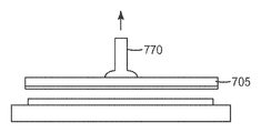
레이저 조사 이후, 지지체는 웨이퍼로부터 분리되며, 이 작업을 위해, 진공을 사용하는 일반적인 픽-업이 사용된다. 픽-업은 원위 단부에 흡입 장치를 갖는 진공 장치에 연결된 원통형 부재이다. 도 7a 및 도 7b는 웨이퍼와 지지체의 분리 작업에 유용한 픽-업의 개략도이다. 도 7a의 경우에, 픽-업(770)은 일반적으로 투광 지지체(705)의 중심에 있으며, 일반적으로 수직 방향으로 픽업되어 지지체를 박리한다. 또한, 도 7b에 도시된 바와 같이, 픽-업(770)은 투광 지지체(705)의 에지부에 있으며, 웨이퍼(702)와 투광 지지체(705) 사이에 공기를 유입시키도록 측부로부터 압축 공기(A)를 송풍하면서 박리시킴으로써 지지체가 보다 쉽게 박리될 수 있다.
지지체 제거 이후, 웨이퍼 상의 결합층이 제거된다. 도 8은 결합층이 박리될 수 있는 방식을 도시하는 개략도이다. 열경화성 결합층(803)의 제거를 위해, 접착 테이프(880)가 사용될 수 있다. 접착 테이프(880)는 열가소성 프라이머 층(806)과 결합층 사이의 접착제 접합보다 열경화성 결합층(803)과 보다 강한 접착제 접합을 형성할 수 있다. 이러한 접착 테이프(880)는 열경화성 결합층(803) 상에 접착하도록 배치될 수 있고, 그 후, 화살표 방향으로 박리될 수 있어서 열경화성 결합층(803)이 프라이밍된 기판(802)으로부터 제거된다.
최종 단계에서, 열가소성 프라이밍 층은 용매 세척에 의해 기판으로부터 제거될 수 있다. 전형적인 용매는 예를 들어, 혼합된 용매로서 3/1 중량비의 N,N-디메틸아세트아미드/1,3-디옥솔란을 포함한다. 전형적으로, N-메틸 파이롤리돈, N,N-디메틸 포름아미드, 디메틸 설폭사이드, 프로필렌 카보네이트, 및 시클로헥사논과 같은 쌍극성 아프로틱(aprotic) 용매가 사용될 수 있다.
마지막으로, 박화된 웨이퍼는 다이 접합 테이프 없이 또는 다이 접합 테이프로 다이싱 테이프 또는 다이 프레임에 고정된 상태로 남아 있는다. 이 웨이퍼는 통상적인 방식으로 다이싱되어 칩을 완성한다. 그러나, 다이싱은 레이저 조사 이전에 수행될 수 있다. 이러한 경우에, 웨이퍼가 지지체에 부착된 상태로 다이싱 단계를 수행하고, 그 후, 다이싱된 영역만을 레이저 조사되게 하고 다이싱된 부분에서만 지지체를 분리시키는 것도 가능하다. 또한, 본 발명은 광열 변환층이 그 위에 제공되어 있는 투광성 지지체 상으로 결합층을 통해 연삭된 웨이퍼를 재전송함으로써 다이싱 테이프를 사용하지 않고 다이싱 단계가 개별적으로 적용될 수도 있다.
제공된 적층체는 기판이 공정에 노출된 상태에서 기판을 보유하기 위해 사용될 수 있다. 이러한 공정은 예를 들어, 이면 연삭, 진공 코팅을 포함하는 코팅, 기상 증착, 에칭, 스트리핑, 화학 처리, 어닐링, 폴리싱, 응력 제거, 결합 또는 부착, 선택적 측정 및 전기 시험을 포함할 수 있다. 고려된 공정은 기판을 약 150℃ 초과, 약 200℃ 초과, 또는 심지어 약 300℃ 초과의 온도에 노출시킬 수 있다.
본 명세서에 개시된 방법은 적층체가 종래 기술의 방법에 비해 더 높은 온도에 노출되도록 허용한다. 반도체 웨이퍼의 제조 시에, 본 발명의 방법은 후속 처리 단계를 허용한다. 이러한 일 예시적인 처리 단계는 예를 들어, 전기 접촉부를 위한 금속 증착 처리와 같은 스퍼터링 기술일 수 있다. 또 다른 이러한 예시적인 처리 단계는 예를 들어, 기판 내에 비아를 생성하기 위한 반응 이온 에칭과 같은 건식 에칭 기술일 수 있다. 또 다른 이러한 예시적인 처리 단계는 예를 들어, 추가 층을 웨이퍼에 접합하는 것과 같은 열-압축 접합일 수 있다. 본 발명의 실시 형태는 결합층이 여전히 연삭된 기판(웨이퍼)로부터 쉽게 제거되면서 적층체가 이들 처리 단계에 노출될 수 있기 때문에 선호된다. 일부 실시 형태에서, 경화된 접착제 결합층을 포함하는 적층체는 200℃ 및 심지어 250℃의 온도에 노출될 수 있다. 본 개시의 실시 형태는 접착제가 또한 기판으로부터 깨끗하게 제거될 수 있으면서 여전히 이의 기계적 일체성을 유지할 수 있고 적어도 한 시간 동안 적어도 250℃로 가열될 수 있도록 제공된다.
일부 실시 형태에서, 박형 열가소성 프라이밍 층은 처리될 기판의 회로(이면)에 도포될 수 있고, 열가소성 프라이머는 도 2에 도시된 바와 같이 에지로부터 제거될 수 있고 프라이머는 건조될 수 있다. 그 후에, 대량의 열경화성 결합층이 스핀 코팅에 의해 그리고 이를 프라이머 층 상에 경화시킴으로써 도포될 수 있다. 박형 열가소성 프라이밍 층의 사용은 유기 및 무기 웨이퍼 표면 재료에 대해 실질적으로 불활성(비반응성)인 웨이퍼 표면(회로측)에 인접한 저 또는 비-탈기 층을 제공하며, 비교적 높은 온도, 예를 들어, 260℃ 초과의 무연 리플로우에 대해 안정적이다. 열가소성 프라이밍 층은 웨이퍼의 회로 측 상의 솔더 볼 또는 범프와 같은 임의의 회로 요소 및 웨이퍼의 소스에 따라 폭 넓게 변화하는 웨이퍼 표면 대신에 열경화성 접착제가 접촉하는 공통 표면 재료를 제공할 수 있다. 열가소성 프라이밍 층은 박리 단계 동안에 레이저 열화로부터 웨이퍼 표면을 보호하기 위하여 열-흡수(적외선(IR)-흡수) 재료로 선택적으로 충전될 수 있는 층을 제공할 수 있다. 열가소성 프라이밍 층은 열경화성 결합층이 박리된 후에 미세 잔류물과 같이 또는 대량으로 제거가능한 용매-용해성 표면을 제공할 수 있으며, 이에 따라 열경화성 결합층으로부터 잔존 가능성이 감소 또는 제거된다. 최종적으로, 열가소성 프라이밍 층을 제거하기 위해 사용되는 가용화 공정 화학물질로부터의 보호는 화학적으로 안정된 열경화성 결합층 재료로의 오버 코팅 및 에지 제거에 의해 제공될 수 있다. 일부 실시 형태에서, 열가소성 프라이밍 층은 투광 지지체 상으로 코팅될 수 있고, 열경화성 결합층은 그 뒤에 열가소성 프라이밍 층에 도포될 수 있으며, 잠재성 이형층은 기판 상에 코팅될 수 있고, 코팅된 지지체 및 기판은 서로 적층될 수 있어서 잠재성 이형층이 결합층에 적층된다. 선택적으로, 열가소성 프라이밍 층은 코팅이 용매를 포함하는 경우 건조될 수 있고, 선택적으로 결합층은 적층 이전에 또는 이후에 경화될 수 있다.
본 발명은 예를 들어, 하기 응용에서 효과적이다.
1. 고-밀도 패키징을 위한 적층형 CSP(칩 크기 패키지)
본 발명은 예를 들어, 복수의 대규모 집적(LSI) 장치 및 수동 부분이 단일 패키지 내에 수용되어 다기능 또는 고성능을 구현하고, 적층된 다중-칩 패키지라 지칭되는 소위 시스템-인-패키지를 형성하는 장치에 유용하다. 본 발명에 따라서, 25 μm 이하의 웨이퍼가 이들 장치를 위한 높은 산출량으로 신뢰성있게 제조될 수 있다.
2. 고 기능 및 고-속 처리를 필요로 하는 관통형 CSP
이 장치에서, 칩은 관통 전극에 의해 접속되며, 그에 의해, 배선 길이가 단축되고 전기적 특성이 향상된다. 관통 전극을 형성하고, 관통 홀 내에 구리를 매설하기 위한 관통 홀의 형성 같은 기술적 문제를 해결하기 위해서, 칩은 두께가 추가로 감소될 수 있다. 본 발명의 적층체를 사용함으로써 이런 구성을 갖는 칩을 순차 형성하는 경우에, 절연막 및 범프(전극)가 웨이퍼의 후방면 상에 형성될 수 있고, 적층체는 열 및 화학물질에 대한 내성이 필요하다. 이런 경우에도, 전술된 지지체, 광열 변환층 및 결합층이 선택될 때, 본 발명이 효과적으로 적용될 수 있다.
3. 방열 효율, 전기적 특성 및 안정성이 향상된 박형 합성 반도체(예를 들어, GaAs)
갈륨 비화물 같은 합성 반도체는 규소보다 그의 유리한 전기적 특성(높은 전자 이동도, 직접 전이형 대역 구조) 때문에 고성능 이산 칩, 레이저 다이오드, 등을 위해 사용되고 있다. 본 발명의 적층체를 사용하여 칩의 두께를 감소시키는 것은 그의 열 소산 효율을 증가시키고, 성능을 향상시킨다. 현재, 전극의 형성 및 두께 감소를 위한 연삭 작업은 그리스(grease) 또는 레지스트 재료를 사용하여 지지체로서의 유리 기판에 반도체 웨이퍼를 결합시킴으로써 수행된다. 따라서, 결합 재료는 처리의 완료 이후 유리 기판으로부터 웨이퍼의 분리를 위해 용매에 의해 용해될 수 있다. 이는 분리에 수일 이상의 시간이 소요되며, 폐기액이 처리되어야 한다는 문제가 동반된다. 본 발명의 적층체가 사용될 때, 이 문제가 해결될 수 있다.
4. 생산성 향상을 위한 대형 웨이퍼에 대한 응용
대형 웨이퍼(예를 들어, 30.5 cm(12 인치)-직경 규소 웨이퍼)의 경우에, 웨이퍼와 지지체를 쉽게 분리시키는 것이 매우 중요하다. 본 발명의 적층체가 사용될 때, 분리가 쉽게 수행될 수 있으며, 따라서, 본 발명은 또한 이 분야에도 적용될 수 있다.
5. 박형 수정 웨이퍼
수정 웨이퍼의 분야에서, 발진 주파수의 증가를 위해 웨이퍼의 두께 감소가 필요하다. 본 발명의 적층체가 사용될 때, 분리가 쉽게 수행될 수 있으며, 따라서, 본 발명은 이 분야에도 또한 적용될 수 있다.
6. 액정 디스플레이를 위한 박형 유리
액정 디스플레이 분야에서, 디스플레이의 중량을 감소시키기 위해 유리의 두께 감소가 요구되며, 유리가 균일한 두께를 갖는 것도 요구된다. 본 발명의 적층체가 사용될 때, 분리가 쉽게 수행될 수 있으며, 따라서, 본 발명은 이 분야에도 또한 적용될 수 있다.
본 발명의 목적과 이점은 하기 예에 의해 추가로 예시되지만 이들 실시예에서 언급된 특정 재료 및 이의 양뿐만 아니라 다른 조건과 세부사항이 본 발명을 지나치게 제한하는 것으로 해석되어서는 안된다.
실시예
시험 방법
박리력 측정
웨이퍼 쿠폰 상에서 EP2020P 코팅과 접착제 조성물 A 사이의 박리력을 측정하기 위한 박리력 측정을 이면 연삭 및 웨이퍼 쿠폰으로부터 유리 지지체의 분리 이후에 수행하였다. 세부사항은 실시예 1 참조. 미국 미네소타 이던 프레리 소재의 MTS 시스템 코포레이션(System Corp)으로부터 입수가능한 30kN 용량을 갖는 인사이트 머테리얼즈 테스팅 시스템(INSIGHT MATERIALS TESTING SYSTEM) 30EL, 820.030-EL에서 박리력 측정을 수행하였다. 미국 미네소타 세인트. 폴 소재의 3M 컴퍼니(Company)로부터 입수가능한 웨이퍼 드-테이핑 테이프(WAFER DE-TAPING TAPE) 3305의 조각을 웨이퍼 쿠폰 상에서 접착제 조성물 A의 표면에 적층하였다. 테이프의 약 75 mm 탭이 쿠폰의 에지로부터 연장되도록 테이프의 크기를 형성하였다. 면도날(razor blade)을 사용하여 테이프 및 하부에 배치된 접착제 내에 약 25 mm 이격된 2개의 평행한 절단부를 형성하였다. 쿠폰을 인장 시험기의 기저 판 고정구 내에서 장착 플레이트 내에 장착하였다. 그 뒤에 75 mm 테이프 탭을 인장 시험 장치의 상부 고정구에 부착하였고, 90° 박리 시험이 125 mm/분의 속도로 수행될 수 있도록 상기 고정구를 수직 부하 셀에 연결하였다.
광학 측정
카본 블랙 충전된 E2020P 폴리아릴에테르설폰 코팅의 광학 측정을 미국 플로리다 더니든 소재의 오션 옵틱스(Ocean Optics)로부터 상표명 니퀘스트(NIRQUEST) 512-2.5로 입수가능한 근적외선 분광기를 사용하여 수행하였다. 결합해제 라이너를 N,N-디메틸아세트아미드/1,3-디옥솔란(2/1) 용매 용액 중에 10%(w/w) 카본 블랙 충전된 E2020P 폴리아릴에테르설폰으로 코팅하였고, 코팅 용액의 제조에 관한 세부사항은 실시예 2를 참조한다. 5분 동안 150℃에서 건조한 이후, 코팅의 두께는 약 20 미크론이었다. 결합해제 라이너를 코팅으로부터 제거하였고, 코팅을 분광기의 검출기와 이미터 사이에 배치하였다. 막을 통한 투과도를 측정하였다.

실시예 1
혼합된 용매 중에 EP2020P의 20%(w/w) 용액, N,N-디메틸아세트아미드 및 1,3-디옥솔란(2/1의 중량) 혼합물을 제조하였다. 용해된 EP2020P와 용액이 완전히 혼합된 후에, 약 2 ㎤의 용액을 주사기를 사용하여 웨이퍼 쿠폰, 솔더 볼 범핑된 반도체 웨이퍼의 100 mm × 100 mm 조각에 배치하였다. 웨이퍼 조각은 각각 직경이 약 85 미크론인 솔더 볼의 규칙적 어레이를 갖는 평평한 폴리이미드 표면을 포함하였다. 용액을 25 초 동안 1,000 rpm에서 스핀 코팅을 통하여 쿠폰 상에 균일하게 코팅하였다. 코팅된 중합체 용액과 웨이퍼 쿠폰을 5 분 동안 150℃의 오븐에서 가열하여 코팅을 건조하였다.
약 2 ㎤의 접착제, 접착제 조성물 A를 주사기를 통하여 쿠폰의 건조된 EP2020P 표면에 적용하였다. 접착제를 25 초 동안 975 rpm에서 스핀 코팅을 통하여 쿠폰 상에 균일하게 코팅하였다. 생성된 접착제 코팅된 웨이퍼 쿠폰을 웨이퍼 지지체 시스템 본더, 모델 번호 WSS 8101M(미국 캘리포니아 프리몬트 소재의 타즈모 컴퍼니(Tazmo Co.)로부터 입수가능함)을 사용하여 151 mm 직경 × 0.7 mm 두께의 유리 지지체에 접합하였다. 유리 지지체는 두께가 1 미크론 미만인 광열 변환층, JS-5000-0012-5(일본 도쿄 소재의 수미토모(Sumitomo) 3M Ltd.(리미티드)로부터 입수가능함)를 포함하였다. 접착제 조성물 A 접착제를 15.2 cm(6 인치) 길이의 퓨전 시스템즈(Fusion Systems) D 전구, 118.1W/cm(300 와트/인치)를 사용하여 20 초 동안 UV 경화하였다.
웨이퍼 쿠폰의 이면을 그 뒤에 통상적인 기술을 사용하여 50 미크론의 두께로 연삭하였다. 접합된 웨이퍼-지지체 스택을 커스텀 이면 열 사이클(customer backside thermal cycling)을 반복하도록 60 분 동안 220℃에서 열 시효하였다. 웨이퍼 또는 유리 지지체의 박리 또는 폴리아릴에테르설폰 및 접착제 조성물 A 층들의 분리가 관찰되지 않았다. 웨이퍼-지지체 스택을 파워라인(Powerline) E 시리즈 레이저(Series laser), 1,064 nm YAG 레이저(독일 스투트가르트 소재의 로핀-시나 테크놀로지스, 인코포레이티드(Rofin-Sinar Technologies, Inc)로부터 입수가능함)를 사용하여 웨이퍼 지지체 시스템 디마운터(wafer support system demounter), 모델 번호 WSS 8101D(미국 캘리포니아 프리몬트 소재의 타즈모 컴퍼니, 리미티드로부터 입수가능함) 내에서 레이저 래스터팅하였다. 래스터링을 200 미크론의 래스터 피치(raster pitch)로 2000 mm/s의 래스터 속도(raster speed)에서 16 와트의 전력에서 수행하였다. 광열 변환층을 분해하였고 유리 지지체를 웨이퍼 쿠폰으로부터 제거하였다.
접착제 조성물 A 접착제를 통상적인 드-테이핑 박리 방법을 사용하여 폴리아릴에테르설폰 층으로부터 분리하였다. 상용 디본더 공구 내에서 성공적인 자동 박리를 위해 필요한 박리력과 상보적인 평균 박리력은 1.22 N/25 mm이었다. E2020P 폴리아릴에테르설폰 코팅을 혼합된 용매, N,N-디메틸아세트아미드/1,3-디옥솔란(3/1의 중량비)을 사용하여 웨이퍼 기판 표면으로부터 용매 세척하였고, 잔류 폴리아릴에테르설폰이 없는 깨끗한 웨이퍼 표면을 산출하였다. 세척을 스핀-스프레이 기술을 사용하여 수행하였고, 용매를 약 500 rpm에서 웨이퍼를 스핀회전하면서 미국 일리노이 콜 시티 소재의 시카고 에어로졸(Chicago Aerosol)로부터 입수가능한 프레발 스프레이어(PREVAL sprayer)를 사용하여 웨이퍼의 표면 상으로 분사하였다.
실시예 2
실시예 2를 하기 예외에 따라 실시예 1에 기재된 것과 유사한 E2020P 용액으로 코팅하였다. 웨이퍼 쿠폰을 E2020P 폴리아릴에테르설폰, 카본 블랙, N,N-디메틸아세트아미드/1,3-디옥솔란(2/1) 용매 용액으로 코팅하였다. E2020P를 용해시키기 위하여 혼합되는 16 중량부의 용매를 4 부의 E2020P에 첨가하였고, 그 후에 2부의 카본 블랙을 첨가하였다. 카본 블랙-폴리아릴에테르설폰 용액을 4 분 동안 2,250 rpm으로 동작하는 미국 사우스 캐롤라이나 랜드럼 소재의 프랙텍 인코포레이티드(FlackTek Inc)로부터 입수가능한 하우스차일드 스피드믹서(Hauschild SPEEDMIXER) DAC 600 FV를 사용하여 혼합하였다. 웨이퍼 쿠폰 상에서 카본 블랙-폴리아릴에테르설폰 용액을 스핀 코팅한 후에, 코팅을 5 분 동안 150℃에서 오븐 내에 쿠폰을 배치함으로써 건조시켰다. 코팅 두께는 약 20 미크론이었다. 이 두께에서, 코팅은 약 99.9%의 IR 차단, 즉 1,064 nm YAG 레이저 파장의 약 0.1%의 투과율을 제공한다. 카본 블랙 충전된 E2020P 폴리아릴에테르설폰 코팅을 그 뒤에 실시예 1에 기재된 동일한 용매 및 스핀-스프레이 기술을 사용하여 웨이퍼 기판 표면으로부터 용매 세척하였다. 용매 세척은 잔류 카본 블랙 또는 폴리아릴에테르설폰이 없는 깨끗한 웨이퍼 표면을 산출하였다.
본 발명에 대한 다양한 변형 및 변경은 본 발명의 범주 및 사상으로부터 벗어남이 없이 당업자에게 명백해질 것이다. 본 발명은 본 명세서에 나타난 예시적인 실시 형태 및 실시예에 의해 부당하게 제한되지 않고 이러한 실시예 및 실시 형태는 단지 본 명세서 하기에서 나타난 청구항 세트에 의해 제한되는 것으로 의도되는 본 발명의 범위에 따라 예시로서 제시되는 것으로 이해하여야 한다. 본 발명에서 언급된 모든 참조는 그 전체가 참조로서 본 명세서에서 포함된다.≪ 1 >
BRIEF DESCRIPTION OF THE DRAWINGS Figure 1 is a side cross-sectional view of an embodiment of a laminate provided.
2,
2 is a side cross-sectional view of another embodiment of the provided laminate.
3A and 3B,
3A and 3B are cross-sectional views showing a vacuum bonding apparatus useful in the present invention.
4a, 4a ', 4b, 4c, 4d and 4e >
Figures 4A, 4A ', 4B, 4C, 4D and 4E show the step of peeling the bond layer and separating the support.
5,
5 is a cross-sectional view of a stack fixture device that can be used in the laser beam irradiation step.
6a, 6b, 6c, 6d, 6e and 6f >
6A, 6B, 6C, 6D, 6E and 6F are perspective views of a laser irradiation apparatus.
7A and 7B,
7A and 7B are schematic diagrams of pick-ups used in the process of separating the wafer and the support.
8,
8 is a schematic diagram illustrating a method in which a bonding layer is peeled off a wafer.
DETAILED DESCRIPTION OF THE INVENTION [
In the following description, reference is made to the accompanying drawings, which form a part of the description of the invention, in which several specific embodiments are shown by way of example. It is to be understood that other embodiments may be contemplated and made without departing from the scope or spirit of the invention. The following detailed description is, therefore, not to be taken in a limiting sense.
Unless otherwise indicated, all numbers expressing feature sizes, amounts, and physical characteristics used in the specification and claims are to be understood as being modified in all instances by the term "about ". Accordingly, unless indicated to the contrary, the numerical parameters set forth in the foregoing specification and attached claims are approximations that may vary depending upon the desired properties sought to be obtained by those skilled in the art using the teachings herein. The use of a numerical range by an end point means that any number within the range (e.g., 1 to 5 includes 1, 1.5, 2, 2.75, 3, 3.80, 4 and 5) ≪ / RTI >
1 is a side cross-sectional view of an embodiment of a laminated
2 is a side cross-sectional view of another embodiment of the laminate 200 provided. The
The laminate includes a light-transmitting support. The light-transmitting substrate is a material capable of transmitting the actinic radiation energy, such as from a laser or a laser diode. The transmittance of the support is not limited unless it does prevent penetration of radiation energy of a practical intensity level into the latent mold release layer to enable decomposition of the latent release layer when the latent release mold layer is photo-activated. Typically, however, the transmittance is, for example, at least 50%. The light-transmitting support typically has a sufficiently high stiffness, and the flexural strength of the support is typically 2 x 10 < RTI ID = 0.0 >-3 (Pa 占 ㎥ 3) or more, more typically 3 占 10-2 (Pa · m 3) or more. Examples of useful supports include glass plates and acrylic plates. In addition, in order to improve the adhesion strength to adjacent layers such as latent release layers, the support may be surface treated with a silane coupling agent, if necessary. When a UV-curable photo-thermal conversion layer or a bonding layer is used, the support typically transmits ultraviolet radiation.
When the photothermal conversion layer is irradiated, the support may be exposed to heat generated in the latent release layer when the latent release layer is photo-activated. Heat resistance, chemical resistance, and low coefficient of expansion. Examples of support materials having these properties are borosilicate glass available as Pyrex and TeMpax and alkaline earth borosilicate glass such as Corning Eagle XG, -aluminosilicate glass.
The provided laminate includes a latent release layer disposed on the light-transmitting support. The latent releasing layer comprises a combination of materials or materials that undergoes a decrease in adhesion in response to external stimuli. External stimuli can be exposure to chemical agents such as heating or cooling, exposure to actinic radiation, strain, humidity, acid or base. In one embodiment, the latent release layer has a glass transition temperature (Tg). ≪ / RTI > The temperature of the laminate, when required to release the bond, is determined by the T value of the latent release layer causing the latent release layer to lose its adhesiong . In another embodiment, the latent release layer is formed, for example, in U.S. Patent Nos. 5,507,464; 6,162,534; 6,410,135; 6,541,089; And 6,821,619 (all of which are disclosed in Hamerski or Hemerski, et al.). In some embodiments, the latent releasing layer is subjected to a chemical radiation or heat application to produce a catalyst such as, for example, an acid catalyst capable of initiating cross-linking, which in turn can reduce the adhesion of the latent release layer Or < / RTI > thermoplastic material. Exemplary catalysts may include a photoacid generator, a latent thermal acid generator, or other potential catalysts well known in the art. In some embodiments, the latent release layer can be a photo-thermal conversion layer.
The photo-thermal conversion layer includes a light absorbing agent and a thermally decomposable resin. The radiation energy applied to the photo-thermal conversion layer in the form of a laser beam, etc. is absorbed by the absorber and converted into heat energy. The generated heat energy rapidly raises the temperature of the photo-thermal conversion layer, and the temperature reaches the thermal decomposition temperature of the thermally decomposed resin (organic component) in the photo-thermal conversion layer, causing thermal decomposition of the resin. It is believed that the gas generated by thermal decomposition forms a void layer (such as space) in the photothermal conversion layer and divides the photothermal conversion layer into two parts, so that any substrate adhered to the support and the laminate is separated . Suitable photo-thermal conversion layers are described, for example, in U.S. Patent No. 7,534,498 (Noda et al.).
The absorber can absorb the actinic radiation at the wavelength used. The radiation energy is typically a laser beam having a wavelength of 300 to 11,000 nanometers (nm), typically 300 to 2,000 nm, a specific example of which is a YAG laser emitting light at a wavelength of 1,064 nm, a YAG laser having a wavelength of 532 nm A second harmonic generation YAG laser, and a semiconductor laser having a wavelength of 780 to 1,300 nm. Although the light absorber varies depending on the wavelength of the laser beam, examples of the light absorber that can be used are carbon black, graphite powder such as microparticles such as iron, aluminum, copper, nickel, cobalt, manganese, chromium, Particulate metal powders such as metal oxide powders, such as black titanium oxide, and metal oxide powders, such as, for example, aromatic diamino-based metal complexes, aliphatic diamine-based metal complexes, Based compounds, aromatic dithiol-based metal complexes, mercaptophenol-based metal complexes, squarylium-based compounds, acyanine- based dyes, methine-based dyes, naphthoquinone-based dyes, and anthraquinone-based dyes. . The absorber may be in the form of a film comprising a vapor-deposited metal film. Among these light absorbing agents, carbon black is particularly useful because carbon black significantly reduces the force required to separate the substrate from the support after irradiation, accelerating the separation.
The concentration of the light absorber in the photothermal conversion layer varies depending on the kind of the light absorber, the particle state (structure) and the degree of dispersion, but in the case of ordinary carbon black having a particle size of about 5 nm to 500 nm, Vol% to 70% by volume. When the concentration is less than 5% by volume, the heat generation of the photo-thermal conversion layer may be insufficient for decomposition of the thermally decomposable resin, and when it exceeds 70% by volume, the film-forming characteristics of the photo- Damage can easily be caused. When the adhesive used as the bonding layer is a UV-curable adhesive, if the amount of carbon black is excessive, the transmittance of ultraviolet rays for curing the adhesive decreases. Therefore, when a UV-curable adhesive is used as the bonding layer, the amount of carbon black should be 60% by volume or less. To prevent abrasion of the photothermal conversion layer during grinding (such as abrasion due to abrasives in the wash water) by reducing the force upon removal of the support after irradiation, the carbon black is added in an amount of from 20% by volume to 60% by volume, Is contained in the photo-thermal conversion layer in an amount of 35% by volume to 55% by volume.
Examples of thermally decomposable resins that can be used include gelatin, cellulose, cellulose esters (e.g., cellulose acetate, nitrocellulose), polyphenols, polyvinyl butyrals, polyvinyl acetals, polycarbonates, polyurethanes, (Meth) acrylate, polyvinyl chloride, silicone resin, and polyurethane units, such as polyvinyl alcohol, polyvinyl alcohol, polyvinyl pyrrolidone, copolymers of vinylidene chloride and acrylonitrile, . These resins may be used individually or in combination of two or more thereof. The glass transition temperature of the resin (Tg) Is typically above room temperature (20 ° C) to prevent re-adhesion of the photo-thermal conversion layer once separated due to formation of the void layer as a result of thermal decomposition of the thermally decomposable resin, and Tg is more typically 100 Lt; / RTI > (For example, -COOH, -OH) that can be hydrogen-bonded to the silanol group on the glass surface in order to increase the adhesion between the glass and the photo-thermal conversion layer when the light-transmitting support is glass A thermally decomposable resin having in the molecule can be used. Further, in applications requiring a chemical liquid treatment such as chemical etching, a thermally decomposable resin having a functional group capable of self-crosslinking at the time of heat treatment in a molecule for imparting chemical resistance to the photo-thermal conversion layer, an ultraviolet ray or visible light Cross-linkable thermally decomposable resins or precursors thereof (e.g., mixtures of monomers and / or oligomers) can be used. To form the photo-thermal conversion layer as the pressure-sensitive adhesive light-heat conversion layer, a pressure-sensitive adhesive polymer formed from poly (meth) acrylate, etc., which may be used for the thermally decomposable resin, may be used.
The photothermal conversion layer may comprise a transparent filler if necessary. The transparent filler functions to prevent re-adhesion of the photo-thermal conversion layer once separated due to the formation of the void layer as a result of thermal decomposition of the thermally decomposable resin. Thus, after grinding and subsequent irradiation of the substrate, the force required for separation of the substrate and the support can be further reduced. Further, since the re-adhesion can be prevented, the range of selection of the thermally decomposable resin is extended. Examples of transparent fillers include silica, mica and barium sulfate. The use of a transparent filler is particularly advantageous when a UV-curable adhesive is used as the bonding layer. This is believed to be due to the following reasons. When a particulate light absorbing agent such as carbon black is used, the light absorbing agent has a function of reducing the force for separation and also functions to prevent the transmission of ultraviolet light. Thus, when a UV-curable adhesive is used as the bonding layer, the curing may not proceed satisfactorily or may require a very long time. In this case, when a transparent filler is used, the substrate and the support can be easily separated after irradiation without interfering with the curing of the UV-curable adhesive. When a particulate light absorbing agent such as carbon black is used, the amount of the transparent filler can be determined by the total amount of the light absorbing agent. The total amount of the transparent filler and particulate light absorbing agent (e.g., carbon black) in the photothermal conversion layer is typically between 5% and 70% by volume based on the volume of the photothermal conversion layer. In the total amount of this range, the force for separation of the substrate and the support can be sufficiently reduced. However, the force for separation is also influenced by the shape of the granular light absorber and the transparent filler. More specifically, the force for separation is sometimes more effectively reduced to a small amount of filler in the case where the particle shape is more complicated (particle state resulting from a more complicated structure) than when a nearly spherical particle shape is relatively simple.
The total amount of particulate absorber and transparent filler may in some cases be determined based on the "top filler volume concentration" (TFVC). This means the filler volume concentration when the mixture of the particulate light absorber and the transparent filler remains in the dry state and the thermally decomposable resin is mixed with the filler in an amount that fits the volume of the pore tightly. That is, the TFVC when the thermally decomposable resin is mixed with an amount of filler that fits the volume of the voids in the mixture of the particulate light absorber and the transparent filler is 100% of the maximum filler volume concentration. The total amount of transparent filler and particulate light absorber in the photothermal conversion layer is typically at least 80%, more typically at least 90% of the maximum filler volume concentration. In a further illustration, the total volume percentage of fillers (e.g., carbon black and transparent filler) is expressed as "A ", and the maximum filler volume concentration (TFVC) (total volume of filler with resin filling void volume of filler A / B is typically greater than about 80% (more typically A / B > 90%).
Although not wishing to be bound by any theory, at present, a light absorbing agent (e.g., carbon black) in a photothermal conversion layer absorbs laser energy irradiated through a transparent support and converts it into heat, Decompose, and produce gas or voids. As a result, the pores separate this layer into two like layers, and then the semiconductor wafer is disengaged from the support. The surface separated by the air gap can contact the surface again at a predetermined time. The surface has not only carbon black particles but also residual resin, and this resin has a reduced molecular weight by thermal decomposition. Upon re-contact (e.g., re-adhesion), this residual resin can increase adhesion. On the other hand, when the adhesive layer as well as the photo-thermal conversion layer are soft, the re-contact area may be relatively large, which makes the adhesion larger and makes it very difficult to unbond the ultra thin wafer from the support without damage or breakage. In the present invention, by setting A / B > 80%, typically A / B > 90%, the residual resin on the unbonded surface is reduced. Thereby, adhesion caused by re-contact can be minimized. In addition, by using the transparent filler to meet the A / B > 80% or 90% and increasing the amount of carbon black, at least a desired thickness can be maintained for the photothermal conversion layer and at the same time, Lt; RTI ID = 0.0 > UV < / RTI > Thus, when the total amount is in this range, the substrate and the support in the thermoplastic priming layer are easily separated after irradiation.
The thickness of the photo-thermal conversion layer is about 0.5 μm. When the thickness is too thin, partial exposure of the adjacent adhesive layer to the bond release surface can occur, which can improve adhesion of the bond release surface, especially when the adhesive layer is relatively soft, Can be difficult.
The photothermal conversion layer may contain other additives as required. For example, when a layer is formed by coating a thermally decomposable resin in the form of a monomer or oligomer, and then the resin is polymerized or cured, the layer may comprise a photo-polymerization initiator. In addition, the addition of a binder to increase the adhesion between the glass and the photo-thermal conversion layer (an integrated blending method, i.e., the binder is used as an additive in the formulation, not as a pre-surface treatment) and a cross- Addition can achieve its respective purpose. Further, in order to promote the decomposition by decomposition of the photo-thermal conversion layer, a low-temperature gas generator may be included. Typical examples of low temperature gas generators that can be used include blowing agents and sublimation agents. Examples of the foaming agent include sodium hydrogencarbonate, ammonium carbonate, ammonium hydrogencarbonate, zinc carbonate, azodicarbonamide, azobisisobutyronitrile, N, N'-dinitrosopentamethylenetetramine, p- p, p-oxybis (benzenesulfonyl hydrazide). Examples of sublimation agents are 2-diazo-5,5-dimethylcyclohexane-1,3-dione, camphor, naphthalene, borneol, butyramide, valeramide valeramide, 4-tert-butylphenol, furan-2-carboxylic acid, succinic anhydride, 1-adamantanol (1 -adamantanol) and 2-adamantanone.
The photothermal conversion layer can be formed by mixing a light absorbing agent such as carbon black, a thermally decomposable resin and a solvent to prepare a precursor coating solution, coating the solution on a support, and drying it. Further, the photothermal conversion layer may be prepared by mixing a monomer or oligomer as a precursor material for a light absorber, a thermally decomposable resin, and optionally an additive such as a photo-polymerization initiator and a solvent as required to prepare a precursor coating solution instead of the heat decomposable resin solution , Coating the solution on a support, drying and polymerizing / curing it. For coating, common coating methods suitable for coating on hard supports such as spin coating, die coating and roll coating may be used. In the case of forming a photothermal conversion layer on a double-sided tape, the photothermal conversion layer may be formed on a film by using a coating method such as die coating, gravure coating and knife coating.
In general, the thickness of the photothermal conversion layer is not limited, but is typically at least 0.1 μm, so long as it allows separation of the support and the substrate with a thermoset priming layer. If the thickness is less than 0.1 탆, the concentration of the absorber required for sufficient absorption is high, which deteriorates the film forming properties and, as a result, adhesion to adjacent layers may become poor. On the other hand, the light transmittance of the photo-thermal conversion layer (or its precursor) is lowered when the thickness of the photo-thermal conversion layer is 5 탆 or more while maintaining a constant light absorber concentration necessary for allowing the photo-thermal conversion layer to be separated by thermal decomposition.
The provided laminate has a bonding layer disposed on the latent-type releasable layer. The bonding layer is a material disposed between and contacting the thermoplastic priming layer and the latent release layer. The bonding layer is attached to both the latent release layer and the thermoplastic priming layer, and is typically an adhesive. The bonding layer may be a thermoplastic material such as epoxy, polyester, polyimide, polycarbonate, polyurethane, polyether, or natural or synthetic rubber. The bond layers can not be cross-linked or can be cross-linked. The bonding layer may also be a thermosetting material, such as a curable polymer or adhesive. Examples of adhesives that can be used as the bonding layer in the provided laminate of the present invention include rubber-based adhesives obtained by dissolving rubber, elastomers, etc. in solvents, 1-part thermosetting adhesives based on epoxy, urethane, epoxy, urethane, (UV) or electron beam curable adhesive based on acrylic, epoxy, and the like, and a water-dispersible adhesive. (1) an oligomer having a polymerizable vinyl group such as urethane acrylate, epoxy acrylate or polyester acrylate, and / or (2) an additive for an acrylic or methacrylic monomer, by adding a photo- The obtained UV-curable adhesive is suitably used. In some embodiments, the bonding layer may comprise a curable (meth) acrylate polymer. Examples of additives include thickeners, plasticizers, dispersants, fillers, fire retardants and heat stabilizers.
In embodiments where the provided laminate further comprises a substrate in contact with the thermoplastic priming layer, the substrate may be a brittle material that is difficult to thin, for example, by conventional methods. Examples thereof include semiconductor wafers such as silicon and gallium arsenide, rock crystal wafers, sapphire and glass. The substrate to be ground may have circuit side and back side. The surface side may include circuit elements such as traces, integrated circuits, electronic components, and conductive connectors such as, for example, solder balls or bumps. Other electrical-connection devices such as pins, sockets, and electrical pads may also be included on the circuit side.
A bonding layer can be used to fix the substrate to be ground through the photo-thermal conversion layer to the support. After separation of the substrate and the support by decomposition of the photo-thermal conversion layer, a substrate having the bonding layer thereon is obtained. Thus, the bonding layer must be easily separated from the substrate, for example by peeling. Thus, the bonding layer is sufficiently high to secure the substrate to the support, but has a bonding strength low enough to allow separation from the substrate. Examples of adhesives which can be used as bonding layers in the present invention include rubber-based adhesives obtained by dissolving rubber, elastomers, etc. in solvents, 1-part thermosetting adhesives based on epoxies, urethanes, etc., epoxies, urethanes, An ultraviolet (UV) or electron beam curable adhesive based on a 2-part thermosetting adhesive, a hot melt adhesive, an acryl, an epoxy, and the like, and a water-dispersible adhesive. (1) an oligomer having a polymerizable vinyl group such as urethane acrylate, epoxy acrylate or polyester acrylate, and / or (2) an additive for an acrylic or methacrylic monomer, by adding a photo- The obtained UV-curable adhesive is suitably used.
In addition to the curable (meth) acrylate polymer, the curable (meth) acrylate adhesion modifier and the photoinitiator, the bonding layer may also include, for example, a reactive diluent. The adhesive binder may comprise a reactive diluent, for example, in an amount ranging from about 10% to about 70% by weight. The reactive diluent may be used to control the viscosity and / or physical properties of the cured composition. Examples of suitable reactive diluents include monofunctional and polyfunctional (meth) acrylate monomers such as ethylene glycol di (meth) acrylate, hexane diol di (meth) acrylate, triethylene glycol di (meth) (Meth) acrylates such as trimethylolpropane tri (meth) acrylate, tripropylene glycol di (meth) acrylate, tetrahydrofurfuryl (meth) acrylate and phenoxyethyl acrylate), vinyl ethers ), Vinyl esters (e.g., vinyl acetate), and styrenic monomers (e.g., styrene).
The substrate to be processed may be, for example, a semiconductor wafer, such as a silicon wafer, which may generally have a rugged portion such as a circuit pattern on one side. For the bonding layer, the adhesive used for the bonding layer is typically in a liquid state during the coating and laminating, to fill the rugged portion of the substrate to be ground and to make the thickness of the bonding layer uniform, And has a viscosity of less than 10,000 centipoise (cps) at a temperature (e.g., 25 占 폚). This liquid adhesive is typically coated by spin coating among various methods described below. UV-curable adhesives and visible light-curable adhesives, which can make the thickness of the bond layer uniform and further increase the processing speed for the reasons mentioned above, are typically used.
The storage modulus of the adhesive is typically 100 MPa or more at 25 DEG C or higher at 25 DEG C after the removal of the solvent of the adhesive in the case of the solvent-based adhesive, after curing in the case of the curable adhesive, or in the condition after solidification at room temperature, It may be 10 MPa or more at 50 캜. With this elastic modulus, the substrate to be ground can be prevented from being distorted or deformed due to the stress imparted during grinding, and can be uniformly ground with the ultra slim substrate. As used herein, the storage modulus or modulus of elasticity is determined, for example, by a temperature gradient of 5 DEG C / min, a strain of 0.04%, and a tensile mode of 1 Hz, with an adhesive sample size of 22.7 mm x 10 mm x 50 m ≪ / RTI > This storage coefficient can be measured using a SOLIDS ANALYZER RSA II (trade name) manufactured by Rheometrics, Inc.
When the photocurable adhesive is cured on the substrate to be ground, the storage coefficient at the maximum achievable temperature (generally 40 占 폚 to 70 占 폚, for example, 50 占 폚) at the interface of the bonding layer and the substrate during grinding is typically 9.0 x 10⁷ Pa, more typically 3.0 x 10 < RTI ID = 0.0 >8 Pa. In the storage coefficients of this range, the vertical pressing by the grinding tool during grinding is prevented from causing local deformation of the bonding layer to the extent that it damages the substrate (silicon wafer) to be ground. Examples of photocurable adhesives satisfying all of these conditions are disclosed in U.S. Patent Application No. 13 / 249,501 (Larson et al.), Entitled " Low Peel Adhesive ", filed September 30, to be.
The thickness of the bonding layer can ensure the thickness uniformity required for grinding of the substrate to be ground and the tear strength necessary for peeling of the bonding layer from the wafer after removal of the support from the laminate, So long as it is capable of adsorbing the same. The thickness of the bonding layer is typically from about 10 [mu] m to about 150 [mu] m, typically from about 25 [mu] m to about 100 [mu] m.
When the bonding layer comprises a curable (meth) acrylate polymer, it may further comprise a certain amount of an adhesion-modifying agent. The bonding layer may comprise a curable (meth) acrylate adhesive-modifier in an amount greater than about 0.1 weight percent or less than about 6.0 weight percent. In some embodiments, the curable (meth) acrylate adhesive-modifier may be a silicone polymer substituted with one or more (meth) acrylate group (s) or methacrylate group (s). Typically, the curable (meth) acrylate adhesive-modifying agent can be dissolved in the curable (meth) acrylate polymer prior to curing. In addition, the viscosity of the combination of the curable (meth) acrylate adhesive-modifier and the curable (meth) acrylate polymer may be less than about 10,000 centipoise at ambient temperature, more preferably less than 5,000 centipoise. For example, the curable (meth) acrylate adhesive-modifier may be EBECRYL 350 from Cytec Industries (West Peterson, NJ), CN9800 from EI Sartomer Company (Exton, Pennsylvania, USA) (Meth) acrylate modified silicone polymer such as TEGO RAD 2250, TEGO RAD 2500, TEGO RAD 2650, or TEGO RAD 2700 from Nick Industries, Essen, Germany.
The provided laminate has a thermoplastic priming layer disposed on the bonding layer. The bonding layer (typically an adhesive layer) is in contact with the thermoplastic priming layer. The thermoplastic priming layer provides a low or non-deagglomerating layer adjacent to any substrate to which this layer contacts. The provided thermoplastic priming layer should be substantially inert (non-reactive) to the organic and inorganic substrate materials and may be stable to a relatively high temperature, for example lead free reflow conditions of 260 占 폚. The thermoplastic priming layer should have high adhesion to both organic and inorganic substrate materials.
The thermoplastic priming layer may also be formed from any circuit element such as a solder ball or bump on the circuit side of the wafer if the substrate is a wafer comprising circuit elements and any common circuit elements that are in contact with the thermosetting adhesive instead of a substrate surface that varies widely depending on the source of the substrate A surface material can be provided. The thermoplastic priming layer may provide a layer that can be selectively filled with a heat-absorbing (IR-absorbing) material to protect the wafer surface from laser degradation during the stripping step. The thermoplastic priming layer can provide a solvent-soluble surface that can be cleaned in bulk or as a fine residue after the thermosetting bonding layer is peeled off, thereby reducing or eliminating the possibility of remaining from the thermosetting bonding layer. Finally, the protection from the solubilising process chemicals used to remove the thermoplastic priming layer can be provided by overcoating and edge removal with chemically stable thermosetting bonding layer materials as shown in Fig.
The thermoplastic priming layer may comprise any thermoplastic material that can be uniformly applied to the surface of the substrate and may include any thermoplastic material that can be applied to the surface of the substrate such as temperature, pressure (such as low pressure), solvent exposure, Of process conditions. Exemplary materials suitable for the thermoplastic priming layer include polyaryl ether sulfone, such as those available under the tradename ULTRASOL E 2020 P POLYARYLETHERSOLFONE from BASF of Flourpark, New Jersey. Others include polyetherimides such as ULTEM or EXTEM available from Sabic, Riyadh, Saudi Arabia, silicone modified polyetherimides such as SILTEM available from SABIC, polyphenylene sulfide (PPS) and polyphenylene sulfide Oxide (PPO).
During the fabrication of the provided laminate, it may be important to prevent undesirable foreign matter such as air from flowing between the layers. For example, when air is introduced between the layers, the thickness uniformity of the laminate is inhibited, and the substrate to be ground may not be ground into a thin substrate. In the case of producing the laminate 100 shown in Fig. 1, for example, the following method can be considered. First, a precursor coating solution of the
The laminate has an adhesive strength between the layers so that when the substrate is a wafer, there is no penetration of water used during grinding of the substrate and the substrate is not separated from the substrate. By the water flow (slurry) including the dust of the ground substrate, Can be designed to have wear resistance to prevent wear. The thinned substrate is prepared by preparing a laminate formed as described above, grinding the substrate to a desired thickness, and applying the radiation energy to the photo-thermal conversion layer through the light-transmitting support to decompose the photo-thermal conversion layer to separate the ground substrate from the light- And peeling the bonding layer from the substrate. The laminate provided can be used to hold the substrate for operations other than backside grinding. Other possible uses for the stack include the retention, deposition, etching, stripping, chemical treatment, annealing, polishing, stress relieving, bonding or adhesion, optical measurement and electrical testing of the substrate during the coating including the vacuum coating .
In one aspect, the method of the present invention is described below with reference to the drawings. Hereinafter, a laser beam is used as a radiation energy source, and a silicon wafer is used as a substrate to be ground, but the present invention is not limited thereto.
3A and 3B are cross-sectional views of a vacuum bonding apparatus suitable for manufacturing a laminate according to an embodiment of the present invention. The
Using the
After the desired level of grinding, the laminate is removed and transferred to a subsequent step, in which the separation of the support and wafer by laser beam irradiation and the peeling of the bonding layer from the wafer are carried out. Figs. 4A to 4E are views showing separation of the support and peeling of the bonding layer. Fig. First, considering the final stage of dicing, the die bonding tape 441 may be disposed (FIG. 4A) on the wafer-side grounded surface of the laminate 401 if necessary, or the die bonding tape 441 (Fig. 4A '). Thereafter, the dicing
Figure 5 is a cross-sectional view of a stack fixture that can be used, for example, in an irradiating step such as using a laser beam of one aspect of the present invention. The laminate 501 is mounted on the fixing
As the laser irradiation apparatus, an apparatus capable of setting the beam moving speed and laser output while scanning the laser beam so as to form a desired pattern on the irradiated surface is selected. Further, in order to stabilize the treatment quality of the irradiated material (laminate), a device having a large focal depth is selected. The focus depth varies with the dimensional accuracy of the design of the device, and is not particularly limited, but the focus depth is typically at least 30 占 퐉. 6A to 6F show a perspective view of a laser irradiation apparatus that can be used in the present invention. The
When considering the wafer damage of the laminate 601 by laser irradiation, a top-hat beam shape (FIG. 6F) having a reduced leakage energy to the adjacent region and a steep energy distribution profile ) Is typically formed. The beam shape may be determined by any known method, for example, by (a) beam deflection method, beam forming method using diffraction / refraction by an acousto-optic device, or (b) It can be changed by a method of cutting.
The laser irradiation energy is determined by the laser power, the beam scanning speed and the beam diameter. For example, the laser power that can be used is 0.3 watts (W) to 100 watts (W), the scan speed is 0.1 to 40 meters / second (m / s) But it is not limited thereto. In order to increase the speed of this step, the laser output is improved, thereby increasing the scanning speed. The number of scans can be further reduced when the beam diameter increases, and the beam diameter can be increased when the laser output is high enough.
After laser irradiation, the support is separated from the wafer, and for this operation, a general pick-up using vacuum is used. The pick-up is a cylindrical member connected to a vacuum device having a suction device at its distal end. Figures 7A and 7B are schematic diagrams of pick-ups useful for separation operations of a wafer and a support. 7A, the pick-
After removal of the support, the bond layer on the wafer is removed. 8 is a schematic view showing a manner in which the bonding layer can be peeled off. To remove the
In the final step, the thermoplastic priming layer can be removed from the substrate by solvent washing. Typical solvents include, for example, 3/1 by weight N, N-dimethylacetamide / 1,3-dioxolane as a mixed solvent. Typically, bipolar aprotic solvents such as N-methyl pyrrolidone, N, N-dimethylformamide, dimethylsulfoxide, propylene carbonate, and cyclohexanone may be used.
Finally, the thinned wafer remains fixed to the dicing tape or die frame without the die bonding tape or with the die bonding tape. The wafer is diced in a conventional manner to complete the chip. However, dicing can be performed before laser irradiation. In this case, it is also possible to carry out the dicing step with the wafer attached to the support, and then let the laser only irradiate the diced region and separate the support only from the diced portion. Further, the present invention may also be applied to the dicing step separately without using the dicing tape by retransferring the wafer ground through the bonding layer onto the light-transmitting substrate on which the photo-thermal conversion layer is provided.
The provided laminate can be used to hold the substrate with the substrate exposed to the process. Such processes may include, for example, backgrinding, coatings including vacuum coating, vapor deposition, etching, stripping, chemical treatment, annealing, polishing, stress relief, bonding or adhesion, selective measurement and electrical testing. The process considered may expose the substrate to temperatures above about 150 ° C, above about 200 ° C, or even above about 300 ° C.
The process disclosed herein allows the laminate to be exposed to higher temperatures than prior art processes. In the manufacture of semiconductor wafers, the method of the present invention allows subsequent processing steps. One such exemplary process step may be a sputtering technique, such as, for example, a metal deposition process for an electrical contact. Another such exemplary processing step may be, for example, a dry etching technique such as reactive ion etching to create vias in a substrate. Another such exemplary processing step may be a heat-compression bonding, for example, bonding an additional layer to a wafer. Embodiments of the present invention are preferred because the laminate can be exposed to these processing steps while the bonding layer is still easily removed from the ground substrate (wafer). In some embodiments, the laminate comprising the cured adhesive bonding layer may be exposed to temperatures of 200 < 0 > C and even 250 < 0 > C. Embodiments of the present disclosure provide that the adhesive can still be cleanly removed from the substrate while still maintaining its mechanical integrity and can be heated to at least 250 캜 for at least one hour.
In some embodiments, a thin thermoplastic priming layer can be applied to the circuit (backside) of the substrate to be treated, the thermoplastic primer can be removed from the edge as shown in Figure 2, and the primer can be dried. A large amount of thermosetting bonding layer can then be applied by spin coating and curing it on the primer layer. The use of a thin thermoplastic priming layer provides a low or non-deagglomerating layer adjacent to a wafer surface (circuit side) that is substantially inert (non-reactive) to organic and inorganic wafer surface materials, and has a relatively high temperature, e.g., 260 RTI ID = 0.0 > C < / RTI > The thermoplastic priming layer can provide a common surface material on which the thermosetting adhesive contacts in place of the wafer surface varying widely depending on the source of the wafer and the source of the wafer and any circuit elements such as solder balls or bumps on the circuit side of the wafer. The thermoplastic priming layer may provide a layer that can be selectively filled with a heat-absorbing (IR-absorbing) material to protect the wafer surface from laser degradation during the stripping step. The thermoplastic priming layer can provide a solvent-soluble surface that can be removed as a fine residue or in large quantities after the thermosetting bonding layer has been peeled off, thereby reducing or eliminating the possibility of remaining from the thermosetting bonding layer. Finally, the protection from the solubilization process chemicals used to remove the thermoplastic priming layer can be provided by overcoating and edge removal with chemically stable thermosetting bonding layer materials. In some embodiments, the thermoplastic priming layer can be coated on the light-pervious support, the thermosetting bonding layer can then be applied to the thermoplastic priming layer, the latent release layer can be coated on the substrate, The substrates may be laminated together so that the latent release layer is laminated to the bonding layer. Optionally, the thermoplastic priming layer can be dried if the coating comprises a solvent, and optionally the bonding layer can be cured before or after lamination.
The present invention is effective, for example, in the following applications.
1. Stacked CSP (chip size package) for high-density packaging
The present invention can be used, for example, in a device that forms a so-called system-in-package, referred to as a stacked multi-chip package, in which a plurality of large scale integrated (LSI) devices and passive parts are housed in a single package to implement multifunctional or high performance, . According to the present invention, wafers of 25 [mu] m or less can be reliably produced with high throughput for these devices.
2. Through-hole CSP requiring high-performance and high-speed processing
In this device, the chip is connected by the penetrating electrode, thereby shortening the wiring length and improving the electrical characteristics. In order to form a penetrating electrode and solve technical problems such as the formation of a through hole for burying copper in the through hole, the chip can be further reduced in thickness. In the case of sequentially forming chips having such a configuration by using the laminate of the present invention, an insulating film and a bump (electrode) can be formed on the rear surface of the wafer, and the laminate is required to have resistance to heat and chemicals Do. Even in this case, the present invention can be effectively applied when the above-described support, photo-thermal conversion layer and bonding layer are selected.
3. Thin synthetic semiconductors (for example, GaAs) with improved heat dissipation efficiency, electrical characteristics and stability,
Synthetic semiconductors, such as gallium arsenide, are being used for high performance discrete chips, laser diodes, etc. because of their advantageous electrical properties (high electron mobility, direct transfer band structure) over silicon. Reducing the thickness of a chip using the laminate of the present invention increases its heat dissipation efficiency and improves performance. Currently, the grinding operation for forming electrodes and reducing the thickness is performed by bonding a semiconductor wafer to a glass substrate as a support using a grease or a resist material. Thus, the bonding material can be dissolved by the solvent for separation of the wafer from the glass substrate after completion of the treatment. This takes time of several days or more to separate and accompanies the problem that waste liquid must be treated. When the laminate of the present invention is used, this problem can be solved.
4. Application to Large Wafer for Productivity Improvement
In the case of large wafers (for example, 30.5 cm (12 inch) -diameter silicon wafers), it is very important to easily separate the wafer and the support. When the laminate of the present invention is used, separation can be easily carried out, and therefore, the present invention can also be applied to this field.
5. Thin thin quartz wafer
In the field of quartz wafers, it is necessary to reduce the wafer thickness in order to increase the oscillation frequency. When the laminate of the present invention is used, the separation can be easily carried out, and therefore, the present invention can also be applied to this field.
6. Thin glass for liquid crystal displays
In the field of liquid crystal displays, a reduction in the thickness of the glass is required to reduce the weight of the display, and it is also required that the glass has a uniform thickness. When the laminate of the present invention is used, the separation can be easily carried out, and therefore, the present invention can also be applied to this field.
The objects and advantages of the present invention are further illustrated by the following examples, but the specific materials and amounts thereof mentioned in these examples, as well as other conditions and details, should not be construed as unduly limiting the present invention.
Example
Test Methods
Peel strength measurement
Peel force measurements to measure the peel force between the EP2020P coating and the adhesive composition A on the wafer coupon were performed after back grinding and after removal of the glass support from the wafer coupon. See Example 1 for details. A peel force measurement was performed on an INSIGHT MATERIALS TESTING SYSTEM 30EL, 820.030-EL having a 30 kN capacity available from MTS System Corp. of Prairie, Minnesota, USA. St. Minnesota, USA. A piece of WAFER DE-TAPING TAPE 3305, available from 3M Company, Pa., Was laminated on the surface of the adhesive composition A on the wafer coupon. The size of the tape was formed such that approximately 75 mm tabs of the tape extended from the edge of the coupon. A razor blade was used to form the tape and two parallel cuts spaced about 25 mm apart in the adhesive disposed thereunder. The coupon was mounted in the mounting plate in the base plate fixture of the tensile testing machine. A 75 mm tape tab was then attached to the upper fixture of the tensile test apparatus and the fixture was connected to the vertical load cell so that the 90 degree peel test could be performed at a rate of 125 mm / min.
Optical measurement
Optical measurements of a carbon black filled E2020P polyaryl ether sulfone coating were performed using a near infrared spectroscope available from Ocean Optics, Dunedin, Florida, under the trade designation NIRQUEST 512-2.5. The release liner was coated with 10% (w / w) carbon black filled E2020P polyaryl ether sulfone in a solvent solution of N, N-dimethylacetamide / 1,3-dioxolane (2/1) See Example 2 for details. After drying at 150 占 폚 for 5 minutes, the thickness of the coating was about 20 microns. The release liner was removed from the coating, and the coating was placed between the detector and the emitter of the spectrometer. The permeability through the membrane was measured.
Example 1
A 20% (w / w) solution of EP2020P, N, N-dimethylacetamide and 1,3-dioxolane (weight of 2/1) mixture was prepared in the mixed solvent. After the solution was completely mixed with the dissolved EP2020P, about 2 cm 3 of the solution was placed in a 100 mm x 100 mm piece of the wafer coupon, solder ball bumped semiconductor wafer, using a syringe. The wafer pieces each contained a flat polyimide surface having a regular array of solder balls each having a diameter of about 85 microns. The solution was uniformly coated on the coupon through spin coating at 1,000 rpm for 25 seconds. The coated polymer solution and the wafer coupon were heated in an oven at < RTI ID = 0.0 > 150 C < / RTI > for 5 minutes to dry the coating.
About 2 cm 3 of the adhesive, Adhesive Composition A, was applied to the surface of the dried EP2020P of the coupon through a syringe. The adhesive was uniformly coated on the coupon through spin coating at 975 rpm for 25 seconds. The resulting adhesive coated wafer coupon was bonded to a 151 mm diameter x 0.7 mm thick glass support using a wafer support system bonder, model number WSS 8101M (available from Tazmo Co., Fremont, CA) Respectively. The glass support contained a photo-thermal conversion layer having a thickness of less than 1 micron, JS-5000-0012-5 (available from Sumitomo 3M Ltd. (Tokyo, Japan)). Adhesive composition A The adhesive was UV cured for 20 seconds using a Fusion Systems D bulb, 6 inches long, 118.1 W / cm (300 watts / inch).
The backside of the wafer coupon was then ground to a thickness of 50 microns using conventional techniques. The bonded wafer-support stack was thermally aged at 220 [deg.] C for 60 minutes to repeat the customer backside thermal cycling. No peeling of the wafer or glass support or separation of the polyaryl ether sulfone and adhesive composition A layers was observed. The wafer-support stack is available from Powerline E-Series Laser, 1,064 nm YAG laser from Rofin-Sinar Technologies, Inc., Stuttgart, Germany. ) Was subjected to laser rasterization in a wafer support system demounter, model number WSS 8101D (available from Tazmo Company, Limited, Fremont, California). The raster ring was performed at a power of 16 watts at a raster speed of 2000 mm / s at a raster pitch of 200 microns. The photothermal conversion layer was disassembled and the glass support was removed from the wafer coupon.
Adhesive composition A Adhesive was separated from the polyaryl ether sulfone layer using a conventional de-taping strip method. The peel force and complementary average peel force required for a successful automatic peel in a commercial Dibonder tool was 1.22 N / 25 mm. E2020P polyaryl ether sulfone coating was solvent-washed from the wafer substrate surface using a mixed solvent, N, N-dimethylacetamide / 1,3-dioxolane (3/1 by weight ratio), and the remaining polyaryl ether sulfone- A clean wafer surface was calculated. Cleaning was performed using a spin-spray technique and the solvent was spin-spinned at about 500 rpm using a PREVAL sprayer available from Chicago Aerosol, ≪ / RTI >
Example 2
Example 2 was coated with an E2020P solution similar to that described in Example 1 with the following exceptions. The wafer coupon was coated with a solvent solution of E2020P polyaryl ether sulfone, carbon black, N, N-dimethylacetamide / 1,3-dioxolane (2/1). 16 parts by weight of solvent mixed to dissolve E2020P was added to 4 parts of E2020P, followed by the addition of 2 parts of carbon black. A carbon black-polyaryl ether sulfone solution was used for 4 minutes using a Hauschild SPEEDMIXER DAC 600 FV available from FlackTek Inc, Lancelad, South Carolina, operating at 2,250 rpm And mixed. After spin-coating the carbon black-polyaryl ether sulfone solution on the wafer coupon, the coating was dried by placing coupons in an oven at 150 占 폚 for 5 minutes. The coating thickness was about 20 microns. At this thickness, the coating provides an IR blocking of about 99.9%, i.e. a transmittance of about 0.1% of a 1,064 nm YAG laser wavelength. A carbon black filled E2020P polyaryl ether sulfone coating was then solvent-washed from the wafer substrate surface using the same solvent and spin-spray technique described in Example 1. Solvent cleaning yielded a clean wafer surface free of residual carbon black or polyaryl ether sulfone.
Various modifications and alterations to this invention will become apparent to those skilled in the art without departing from the scope and spirit of this invention. It is to be understood that the invention is not to be unduly limited by the illustrative embodiments and examples shown herein and that these examples and embodiments are merely illustrative and are not intended to limit the scope of the present invention which is intended to be limited by the claims set forth below. And the like. All references cited herein are incorporated herein by reference in their entirety.
Claims (15)
Applications Claiming Priority (5)
| Application Number | Priority Date | Filing Date | Title |
|---|---|---|---|
| US201261592148P | 2012-01-30 | 2012-01-30 | |
| US61/592,148 | 2012-01-30 | ||
| US201261616568P | 2012-03-28 | 2012-03-28 | |
| US61/616,568 | 2012-03-28 | ||
| PCT/US2013/022844 WO2013116071A1 (en) | 2012-01-30 | 2013-01-24 | Apparatus, hybrid laminated body, method, and materials for temporary substrate support |
Publications (1)
| Publication Number | Publication Date |
|---|---|
| KR20140128355A true KR20140128355A (en) | 2014-11-05 |
Family
ID=48905714
Family Applications (1)
| Application Number | Title | Priority Date | Filing Date |
|---|---|---|---|
| KR20147023802A KR20140128355A (en) | 2012-01-30 | 2013-01-24 | Apparatus, hybrid laminated body, method, and materials for temporary substrate support |
Country Status (6)
| Country | Link |
|---|---|
| US (1) | US20150017434A1 (en) |
| EP (1) | EP2810300A4 (en) |
| JP (1) | JP2015513211A (en) |
| KR (1) | KR20140128355A (en) |
| TW (1) | TW201338104A (en) |
| WO (1) | WO2013116071A1 (en) |
Families Citing this family (14)
| Publication number | Priority date | Publication date | Assignee | Title |
|---|---|---|---|---|
| ITTO20120854A1 (en) * | 2012-09-28 | 2014-03-29 | Stmicroelectronics Malta Ltd | PERFORMED SURFACE MOUNTED CONTAINER FOR AN INTEGRATED SEMICONDUCTOR DEVICE, ITS ASSEMBLY AND MANUFACTURING PROCEDURE |
| JP6193813B2 (en) * | 2014-06-10 | 2017-09-06 | 信越化学工業株式会社 | Temporary adhesive material for wafer processing, wafer processed body, and thin wafer manufacturing method using the same |
| JP6486735B2 (en) * | 2015-03-17 | 2019-03-20 | 東芝メモリ株式会社 | Semiconductor manufacturing method and semiconductor manufacturing apparatus |
| JP2017022213A (en) * | 2015-07-08 | 2017-01-26 | 凸版印刷株式会社 | Printed wiring board |
| US11830756B2 (en) * | 2020-04-29 | 2023-11-28 | Semiconductor Components Industries, Llc | Temporary die support structures and related methods |
| JP6564301B2 (en) * | 2015-10-26 | 2019-08-21 | 東京応化工業株式会社 | Support separation method |
| JP6463664B2 (en) * | 2015-11-27 | 2019-02-06 | 信越化学工業株式会社 | Wafer processing body and wafer processing method |
| EP3248715A4 (en) * | 2016-03-09 | 2018-04-25 | Technology Research Association for Future Additive Manufacturing | 3d additive manufacturing system, 3d additive manufacturing method, additive manufacturing control device, and control method and control program for additive manufacturing control device |
| WO2018062467A1 (en) * | 2016-09-30 | 2018-04-05 | ボンドテック株式会社 | Substrate bonding method and substrate bonding device |
| WO2019106846A1 (en) * | 2017-12-01 | 2019-06-06 | 日立化成株式会社 | Semiconductor device manufacturing method, resin composition for temporary fixation material, laminated film for temporary fixation material |
| KR20210072392A (en) * | 2019-12-09 | 2021-06-17 | 쓰리엠 이노베이티브 프로퍼티즈 컴파니 | Adhesive film |
| KR20220007203A (en) | 2020-07-10 | 2022-01-18 | 삼성전자주식회사 | Method of forming semiconductor package |
| KR20240016994A (en) | 2021-06-03 | 2024-02-06 | 도쿄엘렉트론가부시키가이샤 | Substrate processing method |
| WO2023243488A1 (en) * | 2022-06-13 | 2023-12-21 | 日東電工株式会社 | Adhesive sheet for provisional fixation of electronic component |
Family Cites Families (28)
| Publication number | Priority date | Publication date | Assignee | Title |
|---|---|---|---|---|
| BE754264A (en) * | 1969-08-04 | 1971-02-01 | Uniroyal Inc | THERMOPLASTIC POLYARYLSULFONE RESIN |
| US4231910A (en) * | 1979-02-08 | 1980-11-04 | Dow Corning Corporation | Primer composition |
| US5061549A (en) * | 1990-03-20 | 1991-10-29 | Shores A Andrew | Substrate attach adhesive film, application method and devices incorporating the same |
| US5372883A (en) * | 1990-03-20 | 1994-12-13 | Staystik, Inc. | Die attach adhesive film, application method and devices incorporating the same |
| EP0571649A1 (en) * | 1992-05-26 | 1993-12-01 | Nitto Denko Corporation | Dicing-die bonding film and use thereof in a process for producing chips |
| US5476566A (en) * | 1992-09-02 | 1995-12-19 | Motorola, Inc. | Method for thinning a semiconductor wafer |
| JPH0697017A (en) * | 1992-09-16 | 1994-04-08 | Fujitsu Ltd | Manufacture of semiconductor device |
| JPH1126733A (en) * | 1997-07-03 | 1999-01-29 | Seiko Epson Corp | Transfer method of thin film device, thin film device, thin film integrated circuit device, active matrix substrate, liquid crystal display and electronic equipment |
| JP4565804B2 (en) * | 2002-06-03 | 2010-10-20 | スリーエム イノベイティブ プロパティズ カンパニー | Laminate including ground substrate, method for producing the same, method for producing ultrathin substrate using laminate, and apparatus therefor |
| US6828217B2 (en) * | 2002-10-31 | 2004-12-07 | Northrop Grumman Corporation | Dicing process for GAAS/INP and other semiconductor materials |
| US20060226420A1 (en) * | 2003-07-10 | 2006-10-12 | Matsushita Electric Industrial Co., Ltd. | Organic thin-film transistor and process for fabricating the same, active matrix type display employing it and radio identification tag |
| JP4405246B2 (en) * | 2003-11-27 | 2010-01-27 | スリーエム イノベイティブ プロパティズ カンパニー | Manufacturing method of semiconductor chip |
| JP2006049800A (en) * | 2004-03-10 | 2006-02-16 | Seiko Epson Corp | Thin film device feeder, manufacturing method thereof, transfer method, manufacturing method of semiconductor device, and electronic machine |
| JP4443962B2 (en) * | 2004-03-17 | 2010-03-31 | 日東電工株式会社 | Dicing die bond film |
| US7226812B2 (en) * | 2004-03-31 | 2007-06-05 | Intel Corporation | Wafer support and release in wafer processing |
| US7232740B1 (en) * | 2005-05-16 | 2007-06-19 | The United States Of America As Represented By The National Security Agency | Method for bumping a thin wafer |
| US20080014532A1 (en) * | 2006-07-14 | 2008-01-17 | 3M Innovative Properties Company | Laminate body, and method for manufacturing thin substrate using the laminate body |
| JP4847255B2 (en) * | 2006-08-30 | 2011-12-28 | 株式会社テオス | Processing method of semiconductor wafer |
| US7838391B2 (en) * | 2007-05-07 | 2010-11-23 | Stats Chippac, Ltd. | Ultra thin bumped wafer with under-film |
| US20090017248A1 (en) * | 2007-07-13 | 2009-01-15 | 3M Innovative Properties Company | Layered body and method for manufacturing thin substrate using the layered body |
| US20090017323A1 (en) * | 2007-07-13 | 2009-01-15 | 3M Innovative Properties Company | Layered body and method for manufacturing thin substrate using the layered body |
| JP5224111B2 (en) * | 2008-08-29 | 2013-07-03 | 日立化成株式会社 | Adhesive film for semiconductor wafer processing |
| JP5476046B2 (en) * | 2008-10-03 | 2014-04-23 | 東京応化工業株式会社 | Peeling method, substrate adhesive, and laminate including substrate |
| US8919412B2 (en) * | 2009-04-16 | 2014-12-30 | Suss Microtec Lithography, Gmbh | Apparatus for thermal-slide debonding of temporary bonded semiconductor wafers |
| US8399346B2 (en) * | 2009-09-16 | 2013-03-19 | Brewer Science Inc. | Scratch-resistant coatings for protecting front-side circuitry during backside processing |
| JP5257314B2 (en) * | 2009-09-29 | 2013-08-07 | 大日本印刷株式会社 | LAMINATE, PREPARATION SUPPORT, LAMINATE MANUFACTURING METHOD, AND DEVICE MANUFACTURING METHOD |
| US9263314B2 (en) * | 2010-08-06 | 2016-02-16 | Brewer Science Inc. | Multiple bonding layers for thin-wafer handling |
| US20150034238A1 (en) * | 2012-03-20 | 2015-02-05 | 3M Innovative Properties Company | Laminate body, method, and materials for temporary substrate support and support separation |
-
2013
- 2013-01-24 EP EP13743946.9A patent/EP2810300A4/en not_active Withdrawn
- 2013-01-24 WO PCT/US2013/022844 patent/WO2013116071A1/en active Application Filing
- 2013-01-24 JP JP2014554808A patent/JP2015513211A/en active Pending
- 2013-01-24 KR KR20147023802A patent/KR20140128355A/en not_active Application Discontinuation
- 2013-01-24 US US14/373,953 patent/US20150017434A1/en not_active Abandoned
- 2013-01-29 TW TW102103331A patent/TW201338104A/en unknown
Also Published As
| Publication number | Publication date |
|---|---|
| WO2013116071A1 (en) | 2013-08-08 |
| EP2810300A1 (en) | 2014-12-10 |
| EP2810300A4 (en) | 2016-05-11 |
| US20150017434A1 (en) | 2015-01-15 |
| TW201338104A (en) | 2013-09-16 |
| JP2015513211A (en) | 2015-04-30 |
Similar Documents
| Publication | Publication Date | Title |
|---|---|---|
| KR20140128355A (en) | Apparatus, hybrid laminated body, method, and materials for temporary substrate support | |
| JP4565804B2 (en) | Laminate including ground substrate, method for producing the same, method for producing ultrathin substrate using laminate, and apparatus therefor | |
| JP5048707B2 (en) | Laminate including ground substrate, method for producing the same, method for producing ultrathin substrate using laminate, and apparatus therefor | |
| TWI360888B (en) | Production method of semiconductor chip | |
| US7534498B2 (en) | Laminate body, method, and apparatus for manufacturing ultrathin substrate using the laminate body | |
| US9184083B2 (en) | Apparatus, hybrid laminated body, method and materials for temporary substrate support | |
| US20110031620A1 (en) | Method of thinning a semiconductor substrate | |
| US20090017248A1 (en) | Layered body and method for manufacturing thin substrate using the layered body |
Legal Events
| Date | Code | Title | Description |
|---|---|---|---|
| A201 | Request for examination | ||
| E902 | Notification of reason for refusal | ||
| E601 | Decision to refuse application |