KR20140120823A - Semiconductor device - Google Patents
Semiconductor device Download PDFInfo
- Publication number
- KR20140120823A KR20140120823A KR1020140033981A KR20140033981A KR20140120823A KR 20140120823 A KR20140120823 A KR 20140120823A KR 1020140033981 A KR1020140033981 A KR 1020140033981A KR 20140033981 A KR20140033981 A KR 20140033981A KR 20140120823 A KR20140120823 A KR 20140120823A
- Authority
- KR
- South Korea
- Prior art keywords
- oxide semiconductor
- semiconductor layer
- layer
- oxide
- insulating layer
- Prior art date
Links
- 239000004065 semiconductor Substances 0.000 title claims abstract description 478
- 150000004767 nitrides Chemical class 0.000 claims abstract description 80
- 239000000758 substrate Substances 0.000 claims abstract description 68
- 238000000034 method Methods 0.000 claims abstract description 61
- 239000000203 mixture Substances 0.000 claims abstract description 10
- 238000009413 insulation Methods 0.000 claims 1
- 239000001257 hydrogen Substances 0.000 abstract description 43
- 229910052739 hydrogen Inorganic materials 0.000 abstract description 43
- 239000012535 impurity Substances 0.000 abstract description 32
- 230000008569 process Effects 0.000 abstract description 9
- 125000004435 hydrogen atom Chemical class [H]* 0.000 abstract description 2
- 239000010410 layer Substances 0.000 description 664
- 239000011701 zinc Substances 0.000 description 51
- 239000013078 crystal Substances 0.000 description 44
- 229910052760 oxygen Inorganic materials 0.000 description 38
- UFHFLCQGNIYNRP-UHFFFAOYSA-N Hydrogen Chemical compound [H][H] UFHFLCQGNIYNRP-UHFFFAOYSA-N 0.000 description 37
- QVGXLLKOCUKJST-UHFFFAOYSA-N atomic oxygen Chemical compound [O] QVGXLLKOCUKJST-UHFFFAOYSA-N 0.000 description 36
- 239000001301 oxygen Substances 0.000 description 36
- 238000004544 sputter deposition Methods 0.000 description 36
- 238000010438 heat treatment Methods 0.000 description 35
- 239000004973 liquid crystal related substance Substances 0.000 description 33
- 125000004429 atom Chemical group 0.000 description 27
- IJGRMHOSHXDMSA-UHFFFAOYSA-N Atomic nitrogen Chemical compound N#N IJGRMHOSHXDMSA-UHFFFAOYSA-N 0.000 description 24
- 239000012298 atmosphere Substances 0.000 description 22
- 239000002245 particle Substances 0.000 description 22
- 229910052751 metal Inorganic materials 0.000 description 21
- 239000002184 metal Substances 0.000 description 20
- 206010021143 Hypoxia Diseases 0.000 description 14
- XUIMIQQOPSSXEZ-UHFFFAOYSA-N Silicon Chemical compound [Si] XUIMIQQOPSSXEZ-UHFFFAOYSA-N 0.000 description 14
- 229910052710 silicon Inorganic materials 0.000 description 14
- 239000010703 silicon Substances 0.000 description 14
- 239000003990 capacitor Substances 0.000 description 13
- 239000007789 gas Substances 0.000 description 13
- 229910052757 nitrogen Inorganic materials 0.000 description 12
- 229910052581 Si3N4 Inorganic materials 0.000 description 10
- VYPSYNLAJGMNEJ-UHFFFAOYSA-N Silicium dioxide Chemical compound O=[Si]=O VYPSYNLAJGMNEJ-UHFFFAOYSA-N 0.000 description 10
- 229910052782 aluminium Inorganic materials 0.000 description 10
- 238000004519 manufacturing process Methods 0.000 description 10
- HQVNEWCFYHHQES-UHFFFAOYSA-N silicon nitride Chemical compound N12[Si]34N5[Si]62N3[Si]51N64 HQVNEWCFYHHQES-UHFFFAOYSA-N 0.000 description 10
- 230000015572 biosynthetic process Effects 0.000 description 9
- 229910052814 silicon oxide Inorganic materials 0.000 description 9
- XKRFYHLGVUSROY-UHFFFAOYSA-N Argon Chemical compound [Ar] XKRFYHLGVUSROY-UHFFFAOYSA-N 0.000 description 8
- 230000007547 defect Effects 0.000 description 8
- 229910052733 gallium Inorganic materials 0.000 description 8
- 230000004048 modification Effects 0.000 description 8
- 238000012986 modification Methods 0.000 description 8
- 230000001590 oxidative effect Effects 0.000 description 8
- RTAQQCXQSZGOHL-UHFFFAOYSA-N Titanium Chemical compound [Ti] RTAQQCXQSZGOHL-UHFFFAOYSA-N 0.000 description 7
- 238000004458 analytical method Methods 0.000 description 7
- 229910052799 carbon Inorganic materials 0.000 description 7
- 239000000969 carrier Substances 0.000 description 7
- 238000000151 deposition Methods 0.000 description 7
- 238000005530 etching Methods 0.000 description 7
- 238000005477 sputtering target Methods 0.000 description 7
- 229910052719 titanium Inorganic materials 0.000 description 7
- 239000010936 titanium Substances 0.000 description 7
- XLYOFNOQVPJJNP-UHFFFAOYSA-N water Substances O XLYOFNOQVPJJNP-UHFFFAOYSA-N 0.000 description 7
- 229910001868 water Inorganic materials 0.000 description 7
- 229910052725 zinc Inorganic materials 0.000 description 7
- OKTJSMMVPCPJKN-UHFFFAOYSA-N Carbon Chemical compound [C] OKTJSMMVPCPJKN-UHFFFAOYSA-N 0.000 description 6
- XAGFODPZIPBFFR-UHFFFAOYSA-N aluminium Chemical compound [Al] XAGFODPZIPBFFR-UHFFFAOYSA-N 0.000 description 6
- 238000000231 atomic layer deposition Methods 0.000 description 6
- 230000008021 deposition Effects 0.000 description 6
- 238000010894 electron beam technology Methods 0.000 description 6
- 229910052738 indium Inorganic materials 0.000 description 6
- 229910003437 indium oxide Inorganic materials 0.000 description 6
- PJXISJQVUVHSOJ-UHFFFAOYSA-N indium(iii) oxide Chemical compound [O-2].[O-2].[O-2].[In+3].[In+3] PJXISJQVUVHSOJ-UHFFFAOYSA-N 0.000 description 6
- 239000000463 material Substances 0.000 description 6
- 229910052684 Cerium Inorganic materials 0.000 description 5
- RYGMFSIKBFXOCR-UHFFFAOYSA-N Copper Chemical compound [Cu] RYGMFSIKBFXOCR-UHFFFAOYSA-N 0.000 description 5
- 239000000470 constituent Substances 0.000 description 5
- 229910052802 copper Inorganic materials 0.000 description 5
- 239000010949 copper Substances 0.000 description 5
- 150000002431 hydrogen Chemical class 0.000 description 5
- AMGQUBHHOARCQH-UHFFFAOYSA-N indium;oxotin Chemical compound [In].[Sn]=O AMGQUBHHOARCQH-UHFFFAOYSA-N 0.000 description 5
- 150000002500 ions Chemical class 0.000 description 5
- 229910052746 lanthanum Inorganic materials 0.000 description 5
- 229910044991 metal oxide Inorganic materials 0.000 description 5
- 150000004706 metal oxides Chemical class 0.000 description 5
- 239000000523 sample Substances 0.000 description 5
- 229910052718 tin Inorganic materials 0.000 description 5
- 229910052726 zirconium Inorganic materials 0.000 description 5
- CURLTUGMZLYLDI-UHFFFAOYSA-N Carbon dioxide Chemical compound O=C=O CURLTUGMZLYLDI-UHFFFAOYSA-N 0.000 description 4
- ZOKXTWBITQBERF-UHFFFAOYSA-N Molybdenum Chemical compound [Mo] ZOKXTWBITQBERF-UHFFFAOYSA-N 0.000 description 4
- PXHVJJICTQNCMI-UHFFFAOYSA-N Nickel Chemical compound [Ni] PXHVJJICTQNCMI-UHFFFAOYSA-N 0.000 description 4
- GWEVSGVZZGPLCZ-UHFFFAOYSA-N Titan oxide Chemical compound O=[Ti]=O GWEVSGVZZGPLCZ-UHFFFAOYSA-N 0.000 description 4
- XLOMVQKBTHCTTD-UHFFFAOYSA-N Zinc monoxide Chemical compound [Zn]=O XLOMVQKBTHCTTD-UHFFFAOYSA-N 0.000 description 4
- 229910052783 alkali metal Inorganic materials 0.000 description 4
- 150000001340 alkali metals Chemical class 0.000 description 4
- 229910052784 alkaline earth metal Inorganic materials 0.000 description 4
- 150000001342 alkaline earth metals Chemical class 0.000 description 4
- 229910052786 argon Inorganic materials 0.000 description 4
- 238000004040 coloring Methods 0.000 description 4
- 238000002488 metal-organic chemical vapour deposition Methods 0.000 description 4
- 229910052750 molybdenum Inorganic materials 0.000 description 4
- 239000011733 molybdenum Substances 0.000 description 4
- 238000005268 plasma chemical vapour deposition Methods 0.000 description 4
- 238000001004 secondary ion mass spectrometry Methods 0.000 description 4
- 238000002230 thermal chemical vapour deposition Methods 0.000 description 4
- OGIDPMRJRNCKJF-UHFFFAOYSA-N titanium oxide Inorganic materials [Ti]=O OGIDPMRJRNCKJF-UHFFFAOYSA-N 0.000 description 4
- 229910052721 tungsten Inorganic materials 0.000 description 4
- 239000010937 tungsten Substances 0.000 description 4
- 238000004891 communication Methods 0.000 description 3
- 150000001875 compounds Chemical class 0.000 description 3
- 238000002425 crystallisation Methods 0.000 description 3
- 230000008025 crystallization Effects 0.000 description 3
- 230000005669 field effect Effects 0.000 description 3
- 239000011521 glass Substances 0.000 description 3
- 239000007788 liquid Substances 0.000 description 3
- 230000005012 migration Effects 0.000 description 3
- 238000013508 migration Methods 0.000 description 3
- QGLKJKCYBOYXKC-UHFFFAOYSA-N nonaoxidotritungsten Chemical compound O=[W]1(=O)O[W](=O)(=O)O[W](=O)(=O)O1 QGLKJKCYBOYXKC-UHFFFAOYSA-N 0.000 description 3
- 239000002356 single layer Substances 0.000 description 3
- 239000003381 stabilizer Substances 0.000 description 3
- 239000000126 substance Substances 0.000 description 3
- XOLBLPGZBRYERU-UHFFFAOYSA-N tin dioxide Chemical compound O=[Sn]=O XOLBLPGZBRYERU-UHFFFAOYSA-N 0.000 description 3
- 229910001887 tin oxide Inorganic materials 0.000 description 3
- WFKWXMTUELFFGS-UHFFFAOYSA-N tungsten Chemical compound [W] WFKWXMTUELFFGS-UHFFFAOYSA-N 0.000 description 3
- 229910001930 tungsten oxide Inorganic materials 0.000 description 3
- YVTHLONGBIQYBO-UHFFFAOYSA-N zinc indium(3+) oxygen(2-) Chemical compound [O--].[Zn++].[In+3] YVTHLONGBIQYBO-UHFFFAOYSA-N 0.000 description 3
- VYZAMTAEIAYCRO-UHFFFAOYSA-N Chromium Chemical compound [Cr] VYZAMTAEIAYCRO-UHFFFAOYSA-N 0.000 description 2
- XEEYBQQBJWHFJM-UHFFFAOYSA-N Iron Chemical compound [Fe] XEEYBQQBJWHFJM-UHFFFAOYSA-N 0.000 description 2
- 239000004983 Polymer Dispersed Liquid Crystal Substances 0.000 description 2
- 229910020833 Sn-Al-Zn Inorganic materials 0.000 description 2
- NRTOMJZYCJJWKI-UHFFFAOYSA-N Titanium nitride Chemical compound [Ti]#N NRTOMJZYCJJWKI-UHFFFAOYSA-N 0.000 description 2
- 238000002441 X-ray diffraction Methods 0.000 description 2
- GPBUGPUPKAGMDK-UHFFFAOYSA-N azanylidynemolybdenum Chemical compound [Mo]#N GPBUGPUPKAGMDK-UHFFFAOYSA-N 0.000 description 2
- 230000000903 blocking effect Effects 0.000 description 2
- 229910002092 carbon dioxide Inorganic materials 0.000 description 2
- 239000001569 carbon dioxide Substances 0.000 description 2
- 230000015556 catabolic process Effects 0.000 description 2
- 229910052804 chromium Inorganic materials 0.000 description 2
- 239000011651 chromium Substances 0.000 description 2
- 239000004020 conductor Substances 0.000 description 2
- 238000010586 diagram Methods 0.000 description 2
- 238000001312 dry etching Methods 0.000 description 2
- 230000000694 effects Effects 0.000 description 2
- 230000005684 electric field Effects 0.000 description 2
- 238000002003 electron diffraction Methods 0.000 description 2
- 229910052735 hafnium Inorganic materials 0.000 description 2
- 239000011261 inert gas Substances 0.000 description 2
- 229910010272 inorganic material Inorganic materials 0.000 description 2
- 239000011147 inorganic material Substances 0.000 description 2
- 239000011810 insulating material Substances 0.000 description 2
- 238000005468 ion implantation Methods 0.000 description 2
- MRELNEQAGSRDBK-UHFFFAOYSA-N lanthanum(3+);oxygen(2-) Chemical compound [O-2].[O-2].[O-2].[La+3].[La+3] MRELNEQAGSRDBK-UHFFFAOYSA-N 0.000 description 2
- 239000011159 matrix material Substances 0.000 description 2
- 238000001451 molecular beam epitaxy Methods 0.000 description 2
- 239000002159 nanocrystal Substances 0.000 description 2
- PLDDOISOJJCEMH-UHFFFAOYSA-N neodymium(3+);oxygen(2-) Chemical compound [O-2].[O-2].[O-2].[Nd+3].[Nd+3] PLDDOISOJJCEMH-UHFFFAOYSA-N 0.000 description 2
- 229910052759 nickel Inorganic materials 0.000 description 2
- TWNQGVIAIRXVLR-UHFFFAOYSA-N oxo(oxoalumanyloxy)alumane Chemical compound O=[Al]O[Al]=O TWNQGVIAIRXVLR-UHFFFAOYSA-N 0.000 description 2
- 239000012071 phase Substances 0.000 description 2
- 229910021420 polycrystalline silicon Inorganic materials 0.000 description 2
- 238000012545 processing Methods 0.000 description 2
- 230000000717 retained effect Effects 0.000 description 2
- 229910052715 tantalum Inorganic materials 0.000 description 2
- GUVRBAGPIYLISA-UHFFFAOYSA-N tantalum atom Chemical compound [Ta] GUVRBAGPIYLISA-UHFFFAOYSA-N 0.000 description 2
- -1 tungsten nitride Chemical class 0.000 description 2
- 238000001039 wet etching Methods 0.000 description 2
- 239000011787 zinc oxide Substances 0.000 description 2
- UWCWUCKPEYNDNV-LBPRGKRZSA-N 2,6-dimethyl-n-[[(2s)-pyrrolidin-2-yl]methyl]aniline Chemical compound CC1=CC=CC(C)=C1NC[C@H]1NCCC1 UWCWUCKPEYNDNV-LBPRGKRZSA-N 0.000 description 1
- 229910000838 Al alloy Inorganic materials 0.000 description 1
- 229910018137 Al-Zn Inorganic materials 0.000 description 1
- 229910018573 Al—Zn Inorganic materials 0.000 description 1
- MYMOFIZGZYHOMD-UHFFFAOYSA-N Dioxygen Chemical compound O=O MYMOFIZGZYHOMD-UHFFFAOYSA-N 0.000 description 1
- 229910052692 Dysprosium Inorganic materials 0.000 description 1
- 208000031501 Emergencies Diseases 0.000 description 1
- 229910052691 Erbium Inorganic materials 0.000 description 1
- 229910052693 Europium Inorganic materials 0.000 description 1
- 229910052688 Gadolinium Inorganic materials 0.000 description 1
- GYHNNYVSQQEPJS-UHFFFAOYSA-N Gallium Chemical compound [Ga] GYHNNYVSQQEPJS-UHFFFAOYSA-N 0.000 description 1
- 229910052689 Holmium Inorganic materials 0.000 description 1
- 108010083687 Ion Pumps Proteins 0.000 description 1
- 229910052765 Lutetium Inorganic materials 0.000 description 1
- 229910052779 Neodymium Inorganic materials 0.000 description 1
- OAICVXFJPJFONN-UHFFFAOYSA-N Phosphorus Chemical compound [P] OAICVXFJPJFONN-UHFFFAOYSA-N 0.000 description 1
- 229910052772 Samarium Inorganic materials 0.000 description 1
- 229910000577 Silicon-germanium Inorganic materials 0.000 description 1
- BQCADISMDOOEFD-UHFFFAOYSA-N Silver Chemical compound [Ag] BQCADISMDOOEFD-UHFFFAOYSA-N 0.000 description 1
- 229910020994 Sn-Zn Inorganic materials 0.000 description 1
- 229910009069 Sn—Zn Inorganic materials 0.000 description 1
- 229910052771 Terbium Inorganic materials 0.000 description 1
- 229910052775 Thulium Inorganic materials 0.000 description 1
- ATJFFYVFTNAWJD-UHFFFAOYSA-N Tin Chemical compound [Sn] ATJFFYVFTNAWJD-UHFFFAOYSA-N 0.000 description 1
- 229910052769 Ytterbium Inorganic materials 0.000 description 1
- QCWXUUIWCKQGHC-UHFFFAOYSA-N Zirconium Chemical compound [Zr] QCWXUUIWCKQGHC-UHFFFAOYSA-N 0.000 description 1
- LEVVHYCKPQWKOP-UHFFFAOYSA-N [Si].[Ge] Chemical compound [Si].[Ge] LEVVHYCKPQWKOP-UHFFFAOYSA-N 0.000 description 1
- 230000001133 acceleration Effects 0.000 description 1
- 238000005275 alloying Methods 0.000 description 1
- 229910021417 amorphous silicon Inorganic materials 0.000 description 1
- NWAIGJYBQQYSPW-UHFFFAOYSA-N azanylidyneindigane Chemical compound [In]#N NWAIGJYBQQYSPW-UHFFFAOYSA-N 0.000 description 1
- 230000004888 barrier function Effects 0.000 description 1
- 230000005540 biological transmission Effects 0.000 description 1
- 150000001721 carbon Chemical group 0.000 description 1
- 229910052800 carbon group element Inorganic materials 0.000 description 1
- 239000000919 ceramic Substances 0.000 description 1
- 229910000420 cerium oxide Inorganic materials 0.000 description 1
- 238000005229 chemical vapour deposition Methods 0.000 description 1
- 230000002542 deteriorative effect Effects 0.000 description 1
- 238000009792 diffusion process Methods 0.000 description 1
- AJNVQOSZGJRYEI-UHFFFAOYSA-N digallium;oxygen(2-) Chemical compound [O-2].[O-2].[O-2].[Ga+3].[Ga+3] AJNVQOSZGJRYEI-UHFFFAOYSA-N 0.000 description 1
- 229910001882 dioxygen Inorganic materials 0.000 description 1
- 238000006073 displacement reaction Methods 0.000 description 1
- KBQHZAAAGSGFKK-UHFFFAOYSA-N dysprosium atom Chemical compound [Dy] KBQHZAAAGSGFKK-UHFFFAOYSA-N 0.000 description 1
- 238000005401 electroluminescence Methods 0.000 description 1
- UYAHIZSMUZPPFV-UHFFFAOYSA-N erbium Chemical compound [Er] UYAHIZSMUZPPFV-UHFFFAOYSA-N 0.000 description 1
- 230000001747 exhibiting effect Effects 0.000 description 1
- 239000005262 ferroelectric liquid crystals (FLCs) Substances 0.000 description 1
- 238000011049 filling Methods 0.000 description 1
- 229910001195 gallium oxide Inorganic materials 0.000 description 1
- 230000007274 generation of a signal involved in cell-cell signaling Effects 0.000 description 1
- VBJZVLUMGGDVMO-UHFFFAOYSA-N hafnium atom Chemical compound [Hf] VBJZVLUMGGDVMO-UHFFFAOYSA-N 0.000 description 1
- 229910000449 hafnium oxide Inorganic materials 0.000 description 1
- WIHZLLGSGQNAGK-UHFFFAOYSA-N hafnium(4+);oxygen(2-) Chemical compound [O-2].[O-2].[Hf+4] WIHZLLGSGQNAGK-UHFFFAOYSA-N 0.000 description 1
- 125000005843 halogen group Chemical group 0.000 description 1
- 229910001385 heavy metal Inorganic materials 0.000 description 1
- KJZYNXUDTRRSPN-UHFFFAOYSA-N holmium atom Chemical compound [Ho] KJZYNXUDTRRSPN-UHFFFAOYSA-N 0.000 description 1
- MYMOFIZGZYHOMD-UHFFFAOYSA-O hydridodioxygen(1+) Chemical compound [OH+]=O MYMOFIZGZYHOMD-UHFFFAOYSA-O 0.000 description 1
- 238000007654 immersion Methods 0.000 description 1
- 238000010348 incorporation Methods 0.000 description 1
- APFVFJFRJDLVQX-UHFFFAOYSA-N indium atom Chemical compound [In] APFVFJFRJDLVQX-UHFFFAOYSA-N 0.000 description 1
- 229910052742 iron Inorganic materials 0.000 description 1
- 230000001788 irregular Effects 0.000 description 1
- 229910052747 lanthanoid Inorganic materials 0.000 description 1
- 150000002602 lanthanoids Chemical class 0.000 description 1
- 150000002605 large molecules Chemical class 0.000 description 1
- 238000000608 laser ablation Methods 0.000 description 1
- OHSVLFRHMCKCQY-UHFFFAOYSA-N lutetium atom Chemical compound [Lu] OHSVLFRHMCKCQY-UHFFFAOYSA-N 0.000 description 1
- 229920002521 macromolecule Polymers 0.000 description 1
- 239000000395 magnesium oxide Substances 0.000 description 1
- CPLXHLVBOLITMK-UHFFFAOYSA-N magnesium oxide Inorganic materials [Mg]=O CPLXHLVBOLITMK-UHFFFAOYSA-N 0.000 description 1
- AXZKOIWUVFPNLO-UHFFFAOYSA-N magnesium;oxygen(2-) Chemical compound [O-2].[Mg+2] AXZKOIWUVFPNLO-UHFFFAOYSA-N 0.000 description 1
- 238000005259 measurement Methods 0.000 description 1
- 239000007769 metal material Substances 0.000 description 1
- 229910021421 monocrystalline silicon Inorganic materials 0.000 description 1
- QEFYFXOXNSNQGX-UHFFFAOYSA-N neodymium atom Chemical compound [Nd] QEFYFXOXNSNQGX-UHFFFAOYSA-N 0.000 description 1
- RUFLMLWJRZAWLJ-UHFFFAOYSA-N nickel silicide Chemical compound [Ni]=[Si]=[Ni] RUFLMLWJRZAWLJ-UHFFFAOYSA-N 0.000 description 1
- 229910021334 nickel silicide Inorganic materials 0.000 description 1
- 230000003287 optical effect Effects 0.000 description 1
- BMMGVYCKOGBVEV-UHFFFAOYSA-N oxo(oxoceriooxy)cerium Chemical compound [Ce]=O.O=[Ce]=O BMMGVYCKOGBVEV-UHFFFAOYSA-N 0.000 description 1
- SIWVEOZUMHYXCS-UHFFFAOYSA-N oxo(oxoyttriooxy)yttrium Chemical compound O=[Y]O[Y]=O SIWVEOZUMHYXCS-UHFFFAOYSA-N 0.000 description 1
- BPUBBGLMJRNUCC-UHFFFAOYSA-N oxygen(2-);tantalum(5+) Chemical compound [O-2].[O-2].[O-2].[O-2].[O-2].[Ta+5].[Ta+5] BPUBBGLMJRNUCC-UHFFFAOYSA-N 0.000 description 1
- RVTZCBVAJQQJTK-UHFFFAOYSA-N oxygen(2-);zirconium(4+) Chemical compound [O-2].[O-2].[Zr+4] RVTZCBVAJQQJTK-UHFFFAOYSA-N 0.000 description 1
- 229910052698 phosphorus Inorganic materials 0.000 description 1
- 239000011574 phosphorus Substances 0.000 description 1
- 239000000049 pigment Substances 0.000 description 1
- 238000009832 plasma treatment Methods 0.000 description 1
- 229920000642 polymer Polymers 0.000 description 1
- 229920005591 polysilicon Polymers 0.000 description 1
- 230000001681 protective effect Effects 0.000 description 1
- 239000010453 quartz Substances 0.000 description 1
- 230000005855 radiation Effects 0.000 description 1
- 230000006798 recombination Effects 0.000 description 1
- 230000009467 reduction Effects 0.000 description 1
- 230000003252 repetitive effect Effects 0.000 description 1
- 230000004044 response Effects 0.000 description 1
- 229910052594 sapphire Inorganic materials 0.000 description 1
- 239000010980 sapphire Substances 0.000 description 1
- 229910052706 scandium Inorganic materials 0.000 description 1
- SIXSYDAISGFNSX-UHFFFAOYSA-N scandium atom Chemical compound [Sc] SIXSYDAISGFNSX-UHFFFAOYSA-N 0.000 description 1
- VSZWPYCFIRKVQL-UHFFFAOYSA-N selanylidenegallium;selenium Chemical compound [Se].[Se]=[Ga].[Se]=[Ga] VSZWPYCFIRKVQL-UHFFFAOYSA-N 0.000 description 1
- 229910021332 silicide Inorganic materials 0.000 description 1
- FVBUAEGBCNSCDD-UHFFFAOYSA-N silicide(4-) Chemical compound [Si-4] FVBUAEGBCNSCDD-UHFFFAOYSA-N 0.000 description 1
- HBMJWWWQQXIZIP-UHFFFAOYSA-N silicon carbide Chemical compound [Si+]#[C-] HBMJWWWQQXIZIP-UHFFFAOYSA-N 0.000 description 1
- 229910010271 silicon carbide Inorganic materials 0.000 description 1
- 229910052709 silver Inorganic materials 0.000 description 1
- 239000004332 silver Substances 0.000 description 1
- 239000007787 solid Substances 0.000 description 1
- 239000007790 solid phase Substances 0.000 description 1
- 125000006850 spacer group Chemical group 0.000 description 1
- 238000000859 sublimation Methods 0.000 description 1
- 230000008022 sublimation Effects 0.000 description 1
- MZLGASXMSKOWSE-UHFFFAOYSA-N tantalum nitride Chemical compound [Ta]#N MZLGASXMSKOWSE-UHFFFAOYSA-N 0.000 description 1
- 229910001936 tantalum oxide Inorganic materials 0.000 description 1
- JBQYATWDVHIOAR-UHFFFAOYSA-N tellanylidenegermanium Chemical compound [Te]=[Ge] JBQYATWDVHIOAR-UHFFFAOYSA-N 0.000 description 1
- FRNOGLGSGLTDKL-UHFFFAOYSA-N thulium atom Chemical compound [Tm] FRNOGLGSGLTDKL-UHFFFAOYSA-N 0.000 description 1
- 238000012546 transfer Methods 0.000 description 1
- 229910052723 transition metal Inorganic materials 0.000 description 1
- 230000008016 vaporization Effects 0.000 description 1
- NAWDYIZEMPQZHO-UHFFFAOYSA-N ytterbium Chemical compound [Yb] NAWDYIZEMPQZHO-UHFFFAOYSA-N 0.000 description 1
- 229910052727 yttrium Inorganic materials 0.000 description 1
- VWQVUPCCIRVNHF-UHFFFAOYSA-N yttrium atom Chemical compound [Y] VWQVUPCCIRVNHF-UHFFFAOYSA-N 0.000 description 1
- AKJVMGQSGCSQBU-UHFFFAOYSA-N zinc azanidylidenezinc Chemical compound [Zn++].[N-]=[Zn].[N-]=[Zn] AKJVMGQSGCSQBU-UHFFFAOYSA-N 0.000 description 1
- OYQCBJZGELKKPM-UHFFFAOYSA-N zinc indium(3+) oxygen(2-) Chemical compound [O-2].[Zn+2].[O-2].[In+3] OYQCBJZGELKKPM-UHFFFAOYSA-N 0.000 description 1
- 229910001928 zirconium oxide Inorganic materials 0.000 description 1
Images


Classifications
-
- H—ELECTRICITY
- H01—ELECTRIC ELEMENTS
- H01L—SEMICONDUCTOR DEVICES NOT COVERED BY CLASS H10
- H01L29/00—Semiconductor devices adapted for rectifying, amplifying, oscillating or switching, or capacitors or resistors with at least one potential-jump barrier or surface barrier, e.g. PN junction depletion layer or carrier concentration layer; Details of semiconductor bodies or of electrodes thereof ; Multistep manufacturing processes therefor
- H01L29/66—Types of semiconductor device ; Multistep manufacturing processes therefor
- H01L29/68—Types of semiconductor device ; Multistep manufacturing processes therefor controllable by only the electric current supplied, or only the electric potential applied, to an electrode which does not carry the current to be rectified, amplified or switched
- H01L29/76—Unipolar devices, e.g. field effect transistors
- H01L29/772—Field effect transistors
- H01L29/78—Field effect transistors with field effect produced by an insulated gate
- H01L29/786—Thin film transistors, i.e. transistors with a channel being at least partly a thin film
- H01L29/7869—Thin film transistors, i.e. transistors with a channel being at least partly a thin film having a semiconductor body comprising an oxide semiconductor material, e.g. zinc oxide, copper aluminium oxide, cadmium stannate
-
- H—ELECTRICITY
- H01—ELECTRIC ELEMENTS
- H01L—SEMICONDUCTOR DEVICES NOT COVERED BY CLASS H10
- H01L27/00—Devices consisting of a plurality of semiconductor or other solid-state components formed in or on a common substrate
- H01L27/02—Devices consisting of a plurality of semiconductor or other solid-state components formed in or on a common substrate including semiconductor components specially adapted for rectifying, oscillating, amplifying or switching and having at least one potential-jump barrier or surface barrier; including integrated passive circuit elements with at least one potential-jump barrier or surface barrier
- H01L27/12—Devices consisting of a plurality of semiconductor or other solid-state components formed in or on a common substrate including semiconductor components specially adapted for rectifying, oscillating, amplifying or switching and having at least one potential-jump barrier or surface barrier; including integrated passive circuit elements with at least one potential-jump barrier or surface barrier the substrate being other than a semiconductor body, e.g. an insulating body
- H01L27/1214—Devices consisting of a plurality of semiconductor or other solid-state components formed in or on a common substrate including semiconductor components specially adapted for rectifying, oscillating, amplifying or switching and having at least one potential-jump barrier or surface barrier; including integrated passive circuit elements with at least one potential-jump barrier or surface barrier the substrate being other than a semiconductor body, e.g. an insulating body comprising a plurality of TFTs formed on a non-semiconducting substrate, e.g. driving circuits for AMLCDs
- H01L27/1222—Devices consisting of a plurality of semiconductor or other solid-state components formed in or on a common substrate including semiconductor components specially adapted for rectifying, oscillating, amplifying or switching and having at least one potential-jump barrier or surface barrier; including integrated passive circuit elements with at least one potential-jump barrier or surface barrier the substrate being other than a semiconductor body, e.g. an insulating body comprising a plurality of TFTs formed on a non-semiconducting substrate, e.g. driving circuits for AMLCDs with a particular composition, shape or crystalline structure of the active layer
- H01L27/1225—Devices consisting of a plurality of semiconductor or other solid-state components formed in or on a common substrate including semiconductor components specially adapted for rectifying, oscillating, amplifying or switching and having at least one potential-jump barrier or surface barrier; including integrated passive circuit elements with at least one potential-jump barrier or surface barrier the substrate being other than a semiconductor body, e.g. an insulating body comprising a plurality of TFTs formed on a non-semiconducting substrate, e.g. driving circuits for AMLCDs with a particular composition, shape or crystalline structure of the active layer with semiconductor materials not belonging to the group IV of the periodic table, e.g. InGaZnO
-
- H—ELECTRICITY
- H01—ELECTRIC ELEMENTS
- H01L—SEMICONDUCTOR DEVICES NOT COVERED BY CLASS H10
- H01L27/00—Devices consisting of a plurality of semiconductor or other solid-state components formed in or on a common substrate
- H01L27/02—Devices consisting of a plurality of semiconductor or other solid-state components formed in or on a common substrate including semiconductor components specially adapted for rectifying, oscillating, amplifying or switching and having at least one potential-jump barrier or surface barrier; including integrated passive circuit elements with at least one potential-jump barrier or surface barrier
- H01L27/12—Devices consisting of a plurality of semiconductor or other solid-state components formed in or on a common substrate including semiconductor components specially adapted for rectifying, oscillating, amplifying or switching and having at least one potential-jump barrier or surface barrier; including integrated passive circuit elements with at least one potential-jump barrier or surface barrier the substrate being other than a semiconductor body, e.g. an insulating body
- H01L27/1214—Devices consisting of a plurality of semiconductor or other solid-state components formed in or on a common substrate including semiconductor components specially adapted for rectifying, oscillating, amplifying or switching and having at least one potential-jump barrier or surface barrier; including integrated passive circuit elements with at least one potential-jump barrier or surface barrier the substrate being other than a semiconductor body, e.g. an insulating body comprising a plurality of TFTs formed on a non-semiconducting substrate, e.g. driving circuits for AMLCDs
- H01L27/1255—Devices consisting of a plurality of semiconductor or other solid-state components formed in or on a common substrate including semiconductor components specially adapted for rectifying, oscillating, amplifying or switching and having at least one potential-jump barrier or surface barrier; including integrated passive circuit elements with at least one potential-jump barrier or surface barrier the substrate being other than a semiconductor body, e.g. an insulating body comprising a plurality of TFTs formed on a non-semiconducting substrate, e.g. driving circuits for AMLCDs integrated with passive devices, e.g. auxiliary capacitors
-
- H—ELECTRICITY
- H01—ELECTRIC ELEMENTS
- H01L—SEMICONDUCTOR DEVICES NOT COVERED BY CLASS H10
- H01L29/00—Semiconductor devices adapted for rectifying, amplifying, oscillating or switching, or capacitors or resistors with at least one potential-jump barrier or surface barrier, e.g. PN junction depletion layer or carrier concentration layer; Details of semiconductor bodies or of electrodes thereof ; Multistep manufacturing processes therefor
- H01L29/66—Types of semiconductor device ; Multistep manufacturing processes therefor
- H01L29/68—Types of semiconductor device ; Multistep manufacturing processes therefor controllable by only the electric current supplied, or only the electric potential applied, to an electrode which does not carry the current to be rectified, amplified or switched
- H01L29/76—Unipolar devices, e.g. field effect transistors
- H01L29/772—Field effect transistors
- H01L29/78—Field effect transistors with field effect produced by an insulated gate
- H01L29/786—Thin film transistors, i.e. transistors with a channel being at least partly a thin film
- H01L29/78603—Thin film transistors, i.e. transistors with a channel being at least partly a thin film characterised by the insulating substrate or support
Abstract
Description
본 발명의 일 형태는 반도체 장치와 그 제작 방법에 관한 것이다.One aspect of the present invention relates to a semiconductor device and a manufacturing method thereof.
또한, 본 명세서에서 반도체 장치란, 반도체 특성을 이용하여 기능할 수 있는 장치 전반을 말하며 전기 광학 장치, 반도체 회로, 및 전자 기기는 모두 반도체 장치의 범주에 포함된다.The term " semiconductor device " as used herein refers to an overall device capable of functioning using semiconductor characteristics, and the electro-optical device, the semiconductor circuit, and the electronic device are both included in the category of the semiconductor device.
액정 표시 장치나 발광 표시 장치로 대표되는 플랫 패널 디스플레이의 대부분에 사용되고 있는 트랜지스터는 유리 기판 위에 형성된 비정질(amorphous) 실리콘, 단결정 실리콘, 또는 다결정 실리콘 등 실리콘 반도체로 구성된다. 또한, 상술한 실리콘 반도체를 사용한 트랜지스터는 집적 회로(IC) 등에도 이용되고 있다.A transistor used in most of flat panel displays typified by a liquid crystal display device and a light emitting display device is composed of a silicon semiconductor such as amorphous silicon, monocrystalline silicon, or polycrystalline silicon formed on a glass substrate. The transistor using the above-described silicon semiconductor is also used in an integrated circuit (IC) and the like.
근년에 들어 실리콘 반도체 대신에, 반도체 특성을 나타내는 금속 산화물을 트랜지스터에 사용하는 기술이 주목을 받고 있다. 또한, 본 명세서에서는 반도체 특성을 나타내는 금속 산화물을 산화물 반도체라고 부르기로 한다.In recent years, a technique of using a metal oxide, which exhibits semiconductor characteristics, in transistors instead of silicon semiconductors has attracted attention. In the present specification, a metal oxide showing semiconductor characteristics will be referred to as an oxide semiconductor.
예를 들어, 산화물 반도체로서 산화 아연 또는 In-Ga-Zn계 산화물을 사용한 트랜지스터를 제작하고 이 트랜지스터를 표시 장치에 포함되는 화소의 스위칭 소자 등에 이용하는 기술이 개시(開示)되어 있다(특허문헌 1 및 특허문헌 2 참조).For example, a technique has been disclosed in which a transistor using zinc oxide or an In-Ga-Zn oxide as an oxide semiconductor is fabricated and the transistor is used as a switching element of a pixel included in a display device (see
또한, 표시 장치에 포함되는 화소부를 구동시키기 위한 구동 회로부는 트랜지스터, 용량 소자, 저항 소자 등의 소자를 포함하여 구성된다.The driving circuit portion for driving the pixel portion included in the display device includes elements such as a transistor, a capacitor, and a resistor.
특허문헌 3에는, 화소부에 포함되는 산화물 반도체를 사용한 채널 에치형 트랜지스터(channel-etched transistor)와, 구동 회로에 포함되는 산화물 반도체를 사용한 저항 소자를 동일한 공정으로 형성한 반도체 장치가 개시되어 있다.Patent Document 3 discloses a semiconductor device in which a channel using an oxide semiconductor included in a pixel portion and a resistance element using an oxide semiconductor included in a drive circuit are formed by the same process.
본 발명의 일 형태는 산화물 반도체를 포함하여 구성된 트랜지스터와 산화물 반도체를 포함하여 구성된 저항 소자를 동일한 기판 위에 가진 반도체 장치를 제공하는 것을 과제 중 하나로 한다.One aspect of the present invention is to provide a semiconductor device having a transistor composed of an oxide semiconductor and a resistance element composed of an oxide semiconductor on the same substrate.
또한, 본 발명의 다른 일 형태는 신뢰성이 높은 반도체 장치를 제공하는 것을 과제 중 하나로 한다.Another aspect of the present invention is to provide a highly reliable semiconductor device.
또한, 이들 과제의 기재는 다른 과제의 존재를 방해하는 것은 아니다. 본 발명의 일 형태는 상술한 모든 과제를 해결할 필요는 없는 것으로 한다. 또한, 상술한 것 이외의 과제는 명세서 등의 기재로부터 저절로 명백해지는 것으로, 명세서 등의 기재로부터 상술한 것 이외의 과제가 만들어질 수 있다.Further, the description of these tasks does not hinder the existence of other tasks. One aspect of the present invention does not need to solve all of the above-mentioned problems. In addition, problems other than those described above become obvious from the description of the specification and the like, and problems other than those described above can be made from the description of the specification and the like.
본 발명의 일 형태는 수소를 포함한 질화물 절연층으로 덮인 제 1 산화물 반도체층을 포함하는 저항 소자와, 제 1 산화물 반도체층과 조성이 같고 캐리어 밀도가 다르며 산화물 절연층으로 덮인 제 2 산화물 반도체층을 포함하는 트랜지스터를 구비한 반도체 장치이다. 제 1 산화물 반도체층은 불순물 농도를 증가시키는 처리가 수행됨으로써 제 2 산화물 반도체층보다 캐리어 밀도가 높다. 또한, 제 1 산화물 반도체층은 섬 형상으로 가공된 후에 상기 처리가 그 전체 면에 수행되기 때문에, 질화물 절연층과 접촉되는 영역과 질화물 절연층에 제공된 콘택트 홀에서 전극층과 접촉되는 영역은 동일한 도전성을 가진다. 보다 구체적으로는 예를 들어 이하와 같은 구성으로 할 수 있다.According to an aspect of the present invention, there is provided a semiconductor device comprising: a resistance element including a first oxide semiconductor layer covered with a nitride insulating layer containing hydrogen; a second oxide semiconductor layer having the same composition as the first oxide semiconductor layer, And a transistor including the transistor. The first oxide semiconductor layer is higher in carrier density than the second oxide semiconductor layer by performing the treatment for increasing the impurity concentration. Further, since the first oxide semiconductor layer is processed to have an island shape and then the above process is performed on the entire surface thereof, a region in contact with the nitride insulating layer and a region in contact with the electrode layer in the contact hole provided in the nitride insulating layer have the same conductivity I have. More specifically, for example, the following configuration can be employed.
본 발명의 일 형태는 동일한 기판 위에 제공된 저항 소자 및 트랜지스터를 가지고, 저항 소자는 제 1 산화물 반도체층과, 제 1 산화물 반도체층을 덮는 질화물 절연층과, 질화물 절연층에 제공된 콘택트 홀에서 제 1 산화물 반도체층과 전기적으로 접속된 제 1 전극 및 제 2 전극을 포함하고, 트랜지스터는 게이트 전극층과, 게이트 전극층과 중첩되는 제 2 산화물 반도체층과, 게이트 전극층과 제 2 산화물 반도체층 사이의 절연층과, 제 2 산화물 반도체층을 덮는 산화물 절연층과, 산화물 절연층에 제공된 콘택트 홀에서 제 2 산화물 반도체층과 전기적으로 접속된 제 3 전극 및 제 4 전극을 포함하고, 제 1 산화물 반도체층과 제 2 산화물 반도체층은 조성이 같고, 제 1 산화물 반도체층의 캐리어 밀도는 제 2 산화물 반도체층의 캐리어 밀도보다 높은 반도체 장치이다.One aspect of the present invention is a semiconductor device including a resistance element and a transistor provided on the same substrate, the resistance element including a first oxide semiconductor layer, a nitride insulating layer covering the first oxide semiconductor layer, A first electrode and a second electrode electrically connected to the semiconductor layer, the transistor including a gate electrode layer, a second oxide semiconductor layer overlapping the gate electrode layer, an insulating layer between the gate electrode layer and the second oxide semiconductor layer, An oxide insulating layer covering the second oxide semiconductor layer; and a third electrode and a fourth electrode electrically connected to the second oxide semiconductor layer in a contact hole provided in the oxide insulating layer, wherein the first oxide semiconductor layer and the second oxide semiconductor layer The semiconductor layer has the same composition, the carrier density of the first oxide semiconductor layer is higher than the carrier density of the second oxide semiconductor layer, A.
또한, 본 발명의 일 형태는 동일한 기판 위에 제공된 저항 소자 및 트랜지스터를 가지고, 저항 소자는 제 1 질화물 절연층과, 제 1 질화물 절연층 위의 제 1 산화물 반도체층과, 제 1 산화물 반도체층을 덮는 제 2 질화물 절연층과, 제 2 질화물 절연층에 제공된 콘택트 홀에서 제 1 산화물 반도체층과 전기적으로 접속된 제 1 전극 및 제 2 전극을 포함하고, 트랜지스터는 게이트 전극층과, 게이트 전극층 위의 제 1 질화물 절연층과, 제 1 질화물 절연층 위의 제 1 산화물 절연층과, 제 1 질화물 절연층 및 제 1 산화물 절연층을 개재(介在)하여 게이트 전극층과 중첩되는 제 2 산화물 반도체층과, 제 2 산화물 반도체층을 덮는 제 2 산화물 절연층과, 제 2 산화물 절연층 위의 제 2 질화물 절연층과, 제 2 질화물 절연층 및 제 2 산화물 절연층에 제공된 콘택트 홀에서 제 2 산화물 반도체층과 전기적으로 접속된 제 3 전극 및 제 4 전극을 포함하고, 제 1 산화물 반도체층과 제 2 산화물 반도체층은 조성이 같고, 제 1 산화물 반도체층의 캐리어 밀도는 제 2 산화물 반도체층의 캐리어 밀도보다 높은 반도체 장치이다.According to another aspect of the present invention, there is provided a semiconductor device, comprising: a resistive element and a transistor provided on the same substrate, wherein the resistive element includes a first nitride insulating layer, a first oxide semiconductor layer on the first nitride insulating layer, A second nitride insulating layer; and a first electrode and a second electrode electrically connected to the first oxide semiconductor layer in the contact hole provided in the second nitride insulating layer, wherein the transistor includes a gate electrode layer, a first electrode A second oxide semiconductor layer overlying the gate electrode layer with a first nitride insulating layer and a first oxide insulating layer interposed therebetween, and a second oxide semiconductor layer overlying the second oxide insulating layer, A second oxide insulating layer covering the oxide semiconductor layer; a second nitride insulating layer on the second oxide insulating layer; and a second nitride insulating layer on the second nitride insulating layer and the second oxide insulating layer, Wherein the first oxide semiconductor layer and the second oxide semiconductor layer have the same composition and the carrier density of the first oxide semiconductor layer is different from the carrier density of the second oxide semiconductor layer, Is higher than the carrier density of the semiconductor device.
상기 반도체 장치에 있어서 저항 소자는 제 1 질화물 절연층과 제 1 산화물 반도체층 사이에 제 1 산화물 절연층을 포함하여도 좋다.In the semiconductor device, the resistance element may include a first oxide insulating layer between the first nitride insulating layer and the first oxide semiconductor layer.
또한, 상기 반도체 장치에 있어서 저항 소자에서 캐리어가 흐르는 경로의 길이는 트랜지스터에서 캐리어가 흐르는 경로의 길이보다 길어도 좋다.In the semiconductor device, the length of the path through which the carrier flows in the resistance element may be longer than the length of the path through which the carrier flows in the transistor.
또한, 상기 반도체 장치에 있어서 트랜지스터를 포함한 화소를 복수로 가지는 화소부와, 저항 소자를 포함하는 구동 회로부를 가져도 좋다.The semiconductor device may further include a pixel portion having a plurality of pixels including a transistor and a driver circuit portion including a resistance element.
본 발명의 일 형태에 의하여 산화물 반도체를 포함하여 구성된 트랜지스터와 산화물 반도체를 포함하여 구성된 저항 소자를 동일한 기판 위에 가진 반도체 장치를 제공할 수 있다.According to an aspect of the present invention, a semiconductor device having a transistor including an oxide semiconductor and a resistance element including an oxide semiconductor on the same substrate can be provided.
또한, 본 발명의 일 형태에 의하여 신뢰성이 높은 반도체 장치를 제공할 수 있다.According to an aspect of the present invention, a highly reliable semiconductor device can be provided.
도 1은 반도체 장치의 일 형태를 도시한 평면도 및 단면도.
도 2는 반도체 장치의 제작 방법의 일 형태를 도시한 단면도.
도 3은 반도체 장치의 제작 방법의 일 형태를 도시한 단면도.
도 4는 반도체 장치의 일 형태를 도시한 평면도 및 단면도.
도 5는 반도체 장치의 일 형태를 도시한 단면도.
도 6은 반도체 장치의 일 형태를 도시한 단면도 및 밴드 다이어그램.
도 7은 반도체 장치의 일 형태를 도시한 회로도.
도 8은 반도체 장치의 일 형태를 도시한 단면도.
도 9는 전자 기기의 예를 도시한 도면.BRIEF DESCRIPTION OF DRAWINGS FIG. 1 is a plan view and a cross-sectional view showing one embodiment of a semiconductor device;
2 is a cross-sectional view showing an embodiment of a manufacturing method of a semiconductor device.
3 is a cross-sectional view showing an embodiment of a manufacturing method of a semiconductor device.
4 is a plan view and a cross-sectional view showing one embodiment of a semiconductor device.
5 is a cross-sectional view showing an embodiment of a semiconductor device.
6 is a cross-sectional view and band diagram showing an embodiment of a semiconductor device.
7 is a circuit diagram showing an embodiment of a semiconductor device.
8 is a cross-sectional view showing one embodiment of a semiconductor device.
9 is a view showing an example of an electronic apparatus;
이하에서는 본 발명의 실시형태에 대하여 도면을 사용하여 자세히 설명한다. 다만, 본 발명은 이하의 설명에 한정되지 않고 본 발명의 취지와 그 범위에서 벗어남이 없이 그 형태 및 상세한 사항을 다양하게 변경할 수 있는 것은 당업자라면 용이하게 이해할 수 있다. 따라서, 본 발명은 이하에 기재된 실시형태의 내용에 한정하여 해석되는 것은 아니다. 또한, 이하에서 실시형태를 설명함에 있어서 동일한 부분, 또는 같은 기능을 가진 부분에는 동일한 부호 또는 동일한 해치 패턴을 다른 도면간에 공통적으로 사용하고, 그 반복 설명은 생략한다.Hereinafter, embodiments of the present invention will be described in detail with reference to the drawings. However, the present invention is not limited to the following description, and it is easily understood by those skilled in the art that various changes can be made in form and details without departing from the spirit and scope of the present invention. Therefore, the present invention is not construed as being limited to the contents of the embodiments described below. In the following description of the embodiments, the same reference numerals or the same hatched patterns are commonly used for the same parts or portions having the same functions, and repetitive description thereof will be omitted.
또한, 본 명세서에서 참조하는 각 도면에서는 명료화를 위하여 각 구성의 크기, 막 두께, 또는 영역이 과장되어 있는 경우가 있다. 그래서, 반드시 도면상의 스케일에 한정되지 않는다.In each of the drawings referred to in the present specification, the size, film thickness, or region of each structure may be exaggerated for clarity. Therefore, it is not necessarily limited to the scale on the drawing.
또한, 본 명세서 등에서 "제 1", "제 2" 등의 서수사는 구성 요소의 혼동을 피하기 위하여 붙인 것에 불과하고 구성 요소를 수적으로 한정하는 것은 아니다. 따라서, 예를 들어 "제 1"을 "제 2"로 또는 "제 3" 등으로 적절히 바꿔서 설명할 수 있다.In the present specification and the like, ordinal numbers such as " first ", "second ", and the like are merely attached to avoid confusion of components and are not limited to components numerically. Therefore, for example, "first" may be appropriately changed to "second" or "third".
또한, 트랜지스터의 "소스"나 "드레인"의 기능은 극성이 상이한 트랜지스터를 적용하는 경우나, 회로 동작에서 전류 방향이 변화되는 경우 등에, 서로 바뀔 수 있다. 그러므로, 본 명세서에서는 "소스"나 "드레인"의 용어는 교체하여 사용될 수 있는 것으로 한다.Further, the functions of the "source" and the "drain" of the transistor can be changed with each other, such as when a transistor having a different polarity is applied, when the current direction changes in a circuit operation, or the like. Therefore, the terms "source" and "drain" are used herein interchangeably.
(실시형태 1)(Embodiment 1)
본 실시형태에서는, 본 발명의 일 형태에 따른 반도체 장치 및 반도체 장치의 제작 방법에 대하여 도 1 내지 도 5를 사용하여 설명한다.In this embodiment mode, a method of manufacturing a semiconductor device and a semiconductor device according to an embodiment of the present invention will be described with reference to Figs. 1 to 5. Fig.
<반도체 장치의 구성예><Configuration Example of Semiconductor Device>
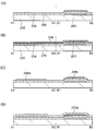
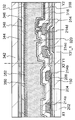
도 1은 반도체 장치의 구성예를 도시한 것이다. 도 1의 (A)는 반도체 장치에 포함되는 저항 소자(150)의 평면도이고, 도 1의 (B)는 반도체 장치에 포함되는 트랜지스터(100)의 평면도이고, 도 1의 (C)는 도 1의 (A)를 A1-A2에서, 도 1의 (B)를 B1-B2에서 각각 절단한 단면도이다. 또한, 도 1의 (A) 및 (B)에서는 도면의 명료화를 위하여 저항 소자(150) 및 트랜지스터(100)의 구성 요소의 일부(질화물 절연층(212) 등)를 생략하여 도시하였다. 이후의 평면도에 관해서도 마찬가지이다.1 shows a configuration example of a semiconductor device. 1 (B) is a plan view of a
도 1에 도시된 트랜지스터(100)는 기판(202) 위에 제공된 게이트 전극층(203)과, 게이트 전극층(203) 위의 절연층(204) 및 절연층(206)과, 절연층(206) 위에 접촉되고 게이트 전극층(203)과 중첩되는 산화물 반도체층(208b)과, 산화물 반도체층(208b)을 덮는 산화물 절연층(210)과, 산화물 절연층(210) 위의 질화물 절연층(212)과, 질화물 절연층(212) 및 산화물 절연층(210)에 제공된 콘택트 홀에서 산화물 반도체층(208b)과 전기적으로 접속된 전극층(214c) 및 전극층(214d)을 포함하여 구성된다.The
또한, 도 1에 도시된 저항 소자(150)는 기판(202) 위에 제공된 산화물 반도체층(208a)과, 산화물 반도체층(208a)을 덮는 질화물 절연층(212)과, 질화물 절연층(212)에 제공된 콘택트 홀에서 산화물 반도체층(208a)과 전기적으로 접속된 전극층(214a) 및 전극층(214b)을 포함하여 구성된다. 또한, 기판(202)과 산화물 반도체층(208a) 사이에 제공된 절연층(204) 및 절연층(206)이 저항 소자(150)의 구성 요소에 포함되어도 좋다.1 also includes an
트랜지스터(100) 및 저항 소자(150)에는 공통적으로 절연층(204), 절연층(206), 및 질화물 절연층(212)이 제공된다. 또한, 트랜지스터(100)에 있어서 절연층(204) 및 절연층(206)은 게이트 절연층에 상당한다. 도 1에는 절연층(204) 및 절연층(206)으로 이루어진 적층 구조를 가진 게이트 절연층을 도시하였지만 게이트 절연층은 단층 구조로 하여도 좋고 3층 이상으로 이루어진 적층 구조로 하여도 좋다. 또한, 전극층(214a) 내지 전극층(214d)은 동일한 공정으로 형성되고, 트랜지스터(100)에 있어서 전극층(214c) 및 전극층(214d)은 한쪽이 소스 전극층에 상당하고 다른 쪽이 드레인 전극층에 상당한다.An
산화물 반도체층(208a) 및 산화물 반도체층(208b)은 동일한 성막 공정과 동일한 에칭 공정을 거쳐 각각 섬 형상으로 가공된 층이다. 산화물 반도체는 막 내의 산소 결손 및/또는 막 내의 수소, 물 등 불순물의 농도에 따라 저항률이 제어될 수 있는 반도체 재료이다. 그러므로, 산화물 반도체층(208a) 및 산화물 반도체층(208b)의 상측(또는 하측)에 접촉되는 각 절연층의 구성을 서로 다르게 함으로써 동일한 공정으로 형성된 각 산화물 반도체층의 저항률을 제어할 수 있다.The
구체적으로는 트랜지스터(100)에서 채널이 형성되는 산화물 반도체층(208b)을 덮는 절연층으로서 산소를 포함하는 절연층(산화물 절연층), 바꿔 말하면 산소를 방출할 수 있는 절연층을 사용함으로써 산화물 반도체층(208b)에 산소를 공급할 수 있다. 산소가 공급된 산화물 반도체층(208b)은 막 내 또는 계면의 산소 결손이 보전되어 저항이 높은 산화물 반도체층이 된다. 또한, 산소를 방출할 수 있는 절연층으로서는 예를 들어, 산화 실리콘층 또는 산화 질화 실리콘층을 사용할 수 있다.More specifically, by using an insulating layer (oxide insulating layer) containing oxygen, in other words, an insulating layer capable of emitting oxygen, as the insulating layer covering the
산소 결손이 보전되고 수소 농도가 저감된 산화물 반도체층(208b)은 고순도 진성화 또는 실질적으로 고순도 진성화된 산화물 반도체층이라고 할 수 있다. 여기서, 실질적으로 진성이란, 산화물 반도체의 캐리어 밀도가 1×10¹⁷/㎤ 미만, 바람직하게는 1×10¹⁵/㎤ 미만, 더 바람직하게는 1×10¹³/㎤ 미만인 것을 말한다. 고순도 진성 또는 실질적으로 고순도 진성인 산화물 반도체는 캐리어 발생원이 적기 때문에 낮은 캐리어 밀도를 가질 수 있다. 또한, 고순도 진성 또는 실질적으로 고순도 진성인 산화물 반도체층(208b)은 결함 준위 밀도가 낮기 때문에 낮은 포획 준위 밀도를 가질 수 있다.The
또한, 고순도 진성 또는 실질적으로 고순도 진성인 산화물 반도체층(208b)은 오프 전류가 매우 낮기 때문에, 채널 폭이 1×10⁶㎛이고 채널 길이(L)가 10㎛인 소자의 경우에도 소스 전극과 드레인 전극간의 전압(드레인 전압)이 1V 내지 10V의 범위 내일 때의 오프 전류가 반도체 파라미터 애널라이저의 측정 한계 이하, 즉 1×10-13A 이하라는 특성을 얻을 수 있다. 따라서 상기 산화물 반도체층(208b)에 채널 영역이 형성되는 트랜지스터(100)는 전기 특성의 변동이 작고 신뢰성이 높은 트랜지스터가 된다.In addition, since the
또한, 산화물 절연층(210)은 저항 소자(150)에 포함되는 산화물 반도체층(208a)과 중첩되는 영역이 선택적으로 제거된다. 따라서, 산화물 반도체층(208a)은 산화물 반도체층(208b)과는 다른 절연층으로 덮인다. 저항 소자(150)에 포함되는 산화물 반도체층(208a)을 덮는 절연층으로서 수소를 포함한 절연층, 바꿔 말하면 수소를 방출할 수 있는 절연층, 대표적으로는 질소를 포함한 무기 절연층, 예를 들어 질화물 절연층을 사용함으로써 산화물 반도체층(208a)에 수소를 공급할 수 있다. 상기 질화물 절연층은 막 내의 함유 수소 농도가 1×10²²atoms/㎤ 이상인 것이 바람직하다. 이와 같은 절연층을 사용함으로써 산화물 반도체층(208a)에 수소를 효과적으로 포함시킬 수 있다.In addition, the
산화물 반도체층(208a)에 포함되는 수소는 금속 원자와 결합된 산소와 반응하여 물이 됨과 동시에, 산소가 탈리된 격자(또는 산소가 탈리된 부분)에 산소 결손을 형성한다. 이 산소 결손에 수소가 들어감으로써 캐리어인 전자가 생성될 수 있다. 또한, 수소의 일부가 금속 원자와 결합된 산소와 결합됨으로써 캐리어인 전자가 생성될 수 있다. 따라서, 수소가 포함되는 산화물 반도체층(208a)은 산화물 반도체층(208b)보다 캐리어 밀도가 높은 산화물 반도체층이다. 바꿔 말하면, 질화물 절연층(212)에 의하여 수소가 공급된 산화물 반도체층(208a)은 저항이 낮은 산화물 반도체층이다.Hydrogen contained in the
트랜지스터(100)에서 채널이 형성되는 산화물 반도체층(208b)은 수소가 가능한 한 저감되는 것이 바람직하다. 구체적으로는, 이차 이온 질량 분석법(SIMS: Secondary Ion Mass Spectrometry)에 의하여 얻어지는 산화물 반도체층(208b)의 수소 농도가 2×10²⁰ atoms/㎤ 이하, 바람직하게는 5×10¹⁹ atoms/㎤ 이하, 더 바람직하게는 1×10¹⁹ atoms/㎤ 이하, 더 바람직하게는 5×10¹⁸ atoms/㎤ 미만, 더 바람직하게는 1×10¹⁸ atoms/㎤ 이하, 더 바람직하게는 5×10¹⁷ atoms/㎤ 이하, 더 바람직하게는 1×10¹⁶atoms/㎤ 이하로 한다. 한편, 저항 소자(150)에 포함되는 산화물 반도체층(208a)은 산화물 반도체층(208b)보다 수소 농도 및/또는 산소 결손량이 많고 저저항화된 산화물 반도체층으로 한다.It is preferable that the amount of hydrogen in the
<반도체 장치의 제작 방법><Manufacturing Method of Semiconductor Device>
도 1에 도시된 반도체 장치의 제작 방법의 일례에 대하여 도 2 및 도 3을 사용하여 설명한다.An example of a manufacturing method of the semiconductor device shown in Fig. 1 will be described with reference to Figs. 2 and 3. Fig.
우선, 기판(202) 위에 게이트 전극층(203)(이와 동일한 층으로 형성되는 배선을 포함함)을 형성하고 게이트 전극층(203) 위에 절연층(204) 및 절연층(206)을 적층한다(도 2의 (A) 참조).First, a gate electrode layer 203 (including a wiring formed of the same layer) is formed on a
기판(202)의 재질 등에 큰 제한은 없지만, 적어도 나중에 수행되는 가열 처리를 견딜 수 있을 정도의 내열성을 가지고 있을 필요가 있다. 예를 들어, 유리 기판, 세라믹 기판, 석영 기판, 사파이어 기판 등을 기판(202)으로서 사용하여도 좋다. 또한, 실리콘이나 탄화 실리콘 등으로 이루어진 단결정 반도체 기판이나 다결정 반도체 기판, 실리콘 게르마늄 등으로 이루어진 화합물 반도체 기판, SOI 기판 등을 적용할 수도 있고, 이와 같은 기판 위에 반도체 소자가 제공된 것을 기판(202)으로서 사용하여도 좋다. 또한, 기판(202)으로서 유리 기판을 사용하는 경우, 제 6 세대(1500㎜×850㎜), 제 7 세대(1870㎜×200㎜), 제 8 세대(2200㎜×400㎜), 제 9 세대(2400㎜×800㎜), 제 10 세대(2950㎜×400㎜) 등의 대면적 기판을 사용하여 대형 표시 장치를 제작할 수 있다.There is no particular limitation on the material of the
또한, 기판(202)으로서 가요성 기판을 사용하고 가요성 기판 위에 직접 트랜지스터(100) 및 저항 소자(150)를 형성하여도 좋다. 또는, 기판(202)과 트랜지스터(100) 및 저항 소자(150)와의 사이에 박리층을 제공하여도 좋다. 박리층은 그 위에 반도체 장치의 일부 또는 전체가 완성된 후에 기판(202)으로부터 분리하고 다른 기판으로 전재(轉載)하는 데 이용할 수 있다. 이 때, 트랜지스터(100) 및 저항 소자(150)는 내열성이 떨어지는 기판이나 가요성 기판에도 전재될 수 있다.The
게이트 전극층(203)은, 몰리브덴, 티타늄, 탄탈, 텅스텐, 알루미늄, 구리, 크롬, 네오디뮴, 스칸듐 등의 금속 재료 또는 이들을 주성분으로 하는 합금 재료를 사용하여 형성할 수 있다. 또한, 인 등 불순물 원소가 도핑된 다결정 실리콘막으로 대표되는 반도체막, 니켈 실리사이드 등의 실리사이드막을 게이트 전극층(203)으로서 사용하여도 좋다. 게이트 전극층(203)은 단층 구조로 하여도 좋고 적층 구조로 하여도 좋다. 게이트 전극층(203)은 테이퍼 형상으로 하여도 좋으며 테이퍼 각은 예를 들어 15° 이상 70° 이하로 하면 좋다. 여기서, 테이퍼 각이란, 테이퍼 형상을 가진 층의 측면과 이 층의 저면 사이의 각도를 말한다.The
또한, 게이트 전극층(203)의 재료로서는 산화 인듐 산화 주석, 산화 텅스텐을 포함한 인듐 산화물, 산화 텅스텐을 포함한 인듐 아연 산화물, 산화 티타늄을 포함한 인듐 산화물, 산화 티타늄을 포함한 인듐 주석 산화물, 산화 인듐 산화 아연, 산화 실리콘이 첨가된 인듐 주석 산화물 등 도전성 재료를 적용할 수도 있다.As the material of the
또는, 게이트 전극층(203)의 재료로서, 질소를 포함한 In-Ga-Zn계 산화물, 질소를 포함한 In-Sn계 산화물, 질소를 포함한 In-Ga계 산화물, 질소를 포함한 In-Zn계 산화물, 질소를 포함한 Sn계 산화물, 질소를 포함한 In계 산화물, 금속 질화물막(질화 인듐막, 질화 아연막, 질화 탄탈막, 질화 텅스텐막 등)을 사용하여도 좋다. 상술한 재료는 5eV 이상의 일함수를 가지므로 상술한 재료를 사용하여 게이트 전극층(203)을 형성하면 트랜지스터의 문턱 전압을 양으로 할 수 있고 노멀리 오프의 스위칭 트랜지스터를 구현할 수 있다. 또한, 게이트 전극층(203)은 스퍼터링법, 플라즈마 CVD법, MOCVD법이나 ALD법 등의 열 CVD법 등으로 형성할 수 있다.In-Zn-based oxide containing nitrogen, In-Sn-based oxide containing nitrogen, In-Ga-based oxide containing nitrogen, In-Zn-containing oxide containing nitrogen, nitrogen An indium oxide containing nitrogen, a metal nitride film (an indium nitride film, a zinc nitride film, a tantalum nitride film, a tungsten nitride film, or the like) may be used. Since the above material has a work function of 5 eV or more, when the
절연층(204) 및 절연층(206)은 트랜지스터(100)의 게이트 절연층에 상당하는 절연층이다. 절연층(204) 및 절연층(206)으로서는 플라즈마 CVD법, 스퍼터링법 등에 의하여 산화 실리콘막, 산화 질화 실리콘막, 질화 산화 실리콘막, 질화 실리콘막, 산화 알루미늄막, 산화 하프늄막, 산화 이트륨막, 산화 지르코늄막, 산화 갈륨막, 산화 탄탈막, 산화 마그네슘막, 산화 란탄막, 산화 세륨막, 및 산화 네오디뮴막 중에서 하나 이상을 포함하는 절연층을 각각 사용할 수 있다. 또한, 절연층(204) 및 절연층(206)으로 이루어진 적층 구조로 하지 않고 상술한 막 중 어느 하나를 포함한 단층 구조의 절연층을 게이트 절연층으로서 사용하여도 좋다.The insulating
또한, 나중에 형성되는 산화물 반도체층(208b)과 접촉되는 절연층(206)은 산화물 절연층인 것이 바람직하고, 화학량론적 조성보다 과잉으로 산소를 포함하는 영역(산소 과잉 영역)을 가지는 것이 더 바람직하다. 절연층(206)에 산소 과잉 영역을 제공하기 위해서는 예를 들어 산소 분위기에서 절연층(206)을 형성하면 좋다. 또는, 형성 후의 절연층(206)에 산소를 도입함으로써 산소 과잉 영역을 형성하여도 좋다. 산소의 도입 방법으로서는 이온 주입법, 이온 도핑법, 플라즈마 잠입 이온 주입법, 플라즈마 처리 등을 사용할 수 있다.Further, the insulating
본 실시형태에서는 절연층(204)으로서 질화 실리콘층을 형성하고 절연층(206)으로서 산화 실리콘층을 형성한다. 질화 실리콘층은 산화 실리콘층에 비하여 비유전율이 높기 때문에, 동등한 정전 용량을 얻는 데 필요한 막 두께가 더 크다. 그래서, 트랜지스터(100)의 게이트 절연층으로서 기능하는 절연층(204)에 질화 실리콘층을 사용하는 경우에는 게이트 절연층을 두껍게 할 수 있다. 따라서, 트랜지스터(100)의 절연 내압이 저하되는 것을 억제할 수 있고, 또한 절연 내압을 향상시켜 트랜지스터의 정전 파괴를 억제할 수 있다. 또한, 절연층(204) 및 절연층(206)은 스퍼터링법, 플라즈마 CVD법, MOCVD법이나 ALD법 등의 열 CVD법 등으로 형성할 수 있다.In this embodiment mode, a silicon nitride layer is formed as the insulating
다음에, 절연층(206) 위에 산화물 반도체막(208)을 형성한다(도 2의 (B) 참조). 산화물 반도체막(208)은 적어도 인듐(In), 아연(Zn), 및 M(Al, Ga, Ge, Y, Zr, Sn, La, Ce, 또는 Hf 등의 금속)을 포함하는 In-M-Zn 산화물로 표기되는 막을 포함하는 것이 바람직하다. 또는, In과 Zn의 양쪽을 포함하는 것이 바람직하다. 또한, 상기 산화물 반도체를 사용한 트랜지스터의 전기 특성의 편차를 저감시키기 위하여 이들과 함께 스테빌라이저(stabilizer)를 포함하는 것이 바람직하다.Next, an
스테빌라이저로서는 갈륨(Ga), 주석(Sn), 하프늄(Hf), 알루미늄(Al), 또는 지르코늄(Zr) 등이 있다. 또한, 이들 외의 스테빌라이저로서는, 란타노이드인, 란탄(La), 세륨(Ce), 프라세오디뮴(Pr), 네오디뮴(Nd), 사마륨(Sm), 유로퓸(Eu), 가돌리늄(Gd), 테르븀(Tb), 디스프로슘(Dy), 홀뮴(Ho), 에르븀(Er), 툴륨(Tm), 이테르븀(Yb), 루테튬(Lu) 등이 있다.Examples of the stabilizer include gallium (Ga), tin (Sn), hafnium (Hf), aluminum (Al), and zirconium (Zr). Examples of other stabilizers include lanthanides La, Ce, Pr, Ne, Sm, Eu, Gd, and Tb ), Dysprosium (Dy), holmium (Ho), erbium (Er), thulium (Tm), ytterbium (Yb), and lutetium (Lu).
산화물 반도체막(208)을 구성하는 산화물 반도체로서, 예를 들어, In-Ga-Zn계 산화물, In-Al-Zn계 산화물, In-Sn-Zn계 산화물, In-Hf-Zn계 산화물, In-La-Zn계 산화물, In-Ce-Zn계 산화물, In-Pr-Zn계 산화물, In-Nd-Zn계 산화물, In-Sm-Zn계 산화물, In-Eu-Zn계 산화물, In-Gd-Zn계 산화물, In-Tb-Zn계 산화물, In-Dy-Zn계 산화물, In-Ho-Zn계 산화물, In-Er-Zn계 산화물, In-Tm-Zn계 산화물, In-Yb-Zn계 산화물, In-Lu-Zn계 산화물, In-Sn-Ga-Zn계 산화물, In-Hf-Ga-Zn계 산화물, In-Al-Ga-Zn계 산화물, In-Sn-Al-Zn계 산화물, In-Sn-Hf-Zn계 산화물, In-Hf-Al-Zn계 산화물을 사용할 수 있다.Zn-based oxide, In-Sn-Zn-based oxide, In-Hf-Zn-based oxide, In-Zn-Zn-based oxide, In- Zn-based oxide, In-Ce-Zn-based oxide, In-Pr-Zn-based oxide, In-Nd-Zn-based oxide, In- In-Zn-based oxide, In-Tb-Zn-based oxide, In-Dy-Zn-based oxide, In-Ho-Zn-based oxide, In- Zn-based oxide, In-Sn-Al-Zn-based oxide, In-Sn-Al-Zn-based oxide, In- In-Sn-Hf-Zn oxide and In-Hf-Al-Zn oxide can be used.
또한 여기서 In-Ga-Zn계 산화물이란, In, Ga, 및 Zn을 주성분으로서 포함하는 산화물을 말하며 In, Ga, 및 Zn의 비율은 불문한다. 또한, In, Ga, 및 Zn 이외의 금속 원소가 들어 있어도 좋다.Here, the In-Ga-Zn-based oxide refers to an oxide containing In, Ga, and Zn as main components, and it does not matter on the ratio of In, Ga, and Zn. In addition, metal elements other than In, Ga, and Zn may be contained.
산화물 반도체막(208)의 성막 방법으로서는 스퍼터링법, MBE(Molecular Beam Epitaxy)법, CVD법, 펄스 레이저 퇴적법, ALD(Atomic Layer Deposition)법 등을 적절히 사용할 수 있다.As the method of forming the
산화물 반도체막(208)을 형성할 때 막 내에 포함되는 수소 농도는 가능한 한 저감시키는 것이 바람직하다. 수소 농도를 저감시키기 위하여 예를 들어, 스퍼터링법으로 형성하는 경우에는 성막실 내의 고진공 배기뿐만 아니라 스퍼터링 가스의 고순도화도 필요하다. 스퍼터링 가스로서, 이슬점이 -40℃ 이하, 바람직하게는 -80℃ 이하, 더 바람직하게는 -100℃ 이하, 더욱 바람직하게는 -120℃ 이하까지 고순도화한 산소 가스나 아르곤 가스를 사용함으로써 산화물 반도체막(208)에 수분 등이 침입되는 것을 가능한 한 방지할 수 있다.When forming the
또한, 성막실 내의 잔류 수분을 제거하기 위해서는, 흡착형 진공 펌프, 예를 들어 크라이오 펌프, 이온 펌프, 티타늄 서블리메이션 펌프를 사용하는 것이 바람직하다. 또한, 터보 분자 펌프에 콜드 트랩을 제공한 것을 사용하여도 좋다. 크라이오 펌프는 예를 들어, 수소 분자, 물(H2O) 등 수소 원자를 포함하는 화합물(더 바람직하게는 탄소 원자를 포함하는 화합물도) 등의 배기 능력이 높기 때문에, 크라이오 펌프를 사용하여 배기한 성막실에서 막을 형성하면 막 내에 포함되는 불순물의 농도를 저감시킬 수 있다.Further, in order to remove the residual moisture in the deposition chamber, it is preferable to use an adsorption-type vacuum pump, for example, a cryopump, an ion pump, and a titanium sublimation pump. Further, a turbo molecular pump provided with a cold trap may be used. The cryo pump uses a cryo pump because it has a high exhausting ability such as a hydrogen molecule, a compound containing a hydrogen atom such as water (H 2 O) (more preferably a compound containing a carbon atom) The concentration of impurities contained in the film can be reduced by forming a film in the exhausted film-forming chamber.
또한, 산화물 반도체막(208)을 스퍼터링법으로 형성하는 경우, 형성에 사용하는 금속 산화물 타깃의 상대 밀도(충전율)는 90% 이상 100% 이하, 바람직하게는 95% 이상 99.9% 이하로 한다. 상대 밀도가 높은 금속 산화물 타깃을 사용함으로써, 형성되는 막을 치밀한 막으로 할 수 있다.When the
또한, 기판(202)을 고온으로 유지한 상태에서 산화물 반도체막(208)을 형성하는 것도, 산화물 반도체막(208) 내에 포함될 수 있는 불순물 농도를 저감시키는 데 유효하다. 기판(202)을 가열하는 온도는 150℃ 이상 450℃ 이하로 하면 좋고, 바람직하게는 기판 온도를 200℃ 이상 350℃ 이하로 하면 좋다.It is also effective to reduce the impurity concentration that can be contained in the
다음에, 산화물 반도체막(208)의 원하는 영역을 가공함으로써 섬 형상의 산화물 반도체층(208d) 및 산화물 반도체층(208b)을 형성한다(도 2의 (C) 참조). 또한, 산화물 반도체막(208)을 에칭으로 가공할 때, 산화물 반도체막(208)의 오버 에칭에 의하여 절연층(206)의 일부(산화물 반도체층(208a) 및 산화물 반도체층(208b)으로 덮이지 않은 영역)가 에칭되어, 막 두께가 감소될 수 있다.Next, a desired region of the
섬 형상의 산화물 반도체층(208d) 및 산화물 반도체층(208b)을 형성한 후에 가열 처리를 수행한다. 가열 처리는 250℃ 이상 650℃ 이하, 바람직하게는 300℃ 이상 400℃ 이하, 더 바람직하게는 320℃ 이상 370℃ 이하의 온도로 불활성 가스 분위기, 산화성 가스를 10ppm 이상 포함한 분위기, 또는 감압 분위기에서 수행하면 좋다. 또한, 이 가열 처리로서는 불활성 가스 분위기에서 가열 처리를 수행한 후에, 탈리된 산소를 보전하기 위하여 산화성 가스를 10ppm 이상 포함한 분위기에서 가열 처리를 수행하여도 좋다. 이 가열 처리에 의하여, 절연층(204), 절연층(206), 산화물 반도체층(208d) 및 산화물 반도체층(208b) 중 적어도 하나에서 수소나 물 등 불순물을 제거할 수 있다. 또한, 이 가열 처리는 산화물 반도체막(208)을 섬 형상으로 가공하기 전에 수행하여도 좋다.After the island-shaped
또한, 산화물 반도체를 채널로 하는 트랜지스터(100)에 안정된 전기 특성을 부여하기 위해서는 산화물 반도체 내의 불순물 농도를 저감시키고 산화물 반도체를 진성 또는 실질적으로 진성으로 하는 것이 유효하다.In order to impart stable electric characteristics to the
다음에, 산화물 반도체층(208d) 및 산화물 반도체층(208b) 위에 산화물 절연막(210a)을 형성한다(도 2의 (D) 참조).Next, an
산화물 절연막(210a)으로서는 예를 들어, 두께 150㎚ 이상 400㎚ 이하의 산화 실리콘막, 산화 질화 실리콘막, 산화 알루미늄막 등을 사용할 수 있다. 본 실시형태에서는 산화물 절연막(210a)으로서 두께 300㎚의 산화 질화 실리콘막을 사용한다. 또한, 산화물 절연막(210a)은 예를 들어, CVD법으로 형성할 수 있다.As the
다음에, 산화물 절연막(210a)의 원하는 영역을 가공하여 개구부(302)를 형성한다. 이에 의하여 산화물 절연막(210a)은 개구부(302)가 형성된 산화물 절연층(210)이 된다.Next, a desired region of the
또한, 개구부(302)는 산화물 반도체층(208a)이 노출되도록 형성한다. 개구부(302)의 형성 방법으로서는, 예를 들어 드라이 에칭법을 사용할 수 있다. 다만, 개구부(302)의 형성 방법은 이에 한정되지 않고 웨트 에칭법, 또는 드라이 에칭법과 웨트 에칭법을 조합한 형성 방법으로 하여도 좋다. 또한, 개구부(302)를 형성하기 위한 에칭 공정에 의하여, 산화물 절연층(210)으로 덮이지 않은 절연층(206)의 일부 및 산화물 반도체층(208a)의 막 두께가 감소될 수 있다.The
이 후 가열 처리를 수행하는 것이 바람직하다. 가열 처리를 수행함으로써 산화물 절연층(210)에 포함되는 산소의 일부를 산화물 반도체층(208b)으로 이동시켜 산화물 반도체층(208b) 내의 산소 결손을 보전할 수 있다. 이 결과 산화물 반도체층(208b)에 포함되는 산소 결손량을 저감시킬 수 있다. 한편, 산화물 절연층(210)과 접촉되지 않는 산화물 반도체층(208d)의 산소 결손량은 저감되지 않기 때문에 산화물 반도체층(208d)은 산화물 반도체층(208b)보다 산소 결손을 많이 포함하게 된다. 가열 처리의 조건은 산화물 반도체층(208d) 및 산화물 반도체층(208b) 형성 후의 가열 처리와 마찬가지로 할 수 있다.It is preferable to carry out a heat treatment thereafter. A part of the oxygen included in the
다음에, 산화물 절연층(210) 및 산화물 반도체층(208d) 위에 질화물 절연층(212)을 형성한다(도 3의 (B) 참조).Next, a
질화물 절연층(212)은 수소를 포함하여 구성된다. 질화물 절연층(212)의 수소는, 산화물 반도체층(208d)에 확산되면 이 산화물 반도체층(208d)에서 산소 결손과 결합하여, 캐리어인 전자를 생성시킨다. 이 결과 산화물 반도체층(208d)은 저항이 낮은 산화물 반도체층(208a)이 된다. 산화물 반도체층(208a)의 저항률은 적어도 산화물 반도체층(208b)보다 낮고 바람직하게는 1×10⁻³Ωcm 이상 1×10⁴Ωcm 미만, 더 바람직하게는 1×10⁻³Ωcm 이상 1×10⁻¹Ωcm 미만이면 좋다. 또한, 질화물 절연층(212)은 외부로부터의 불순물, 예를 들어 물, 알칼리 금속, 알칼리 토금속 등이 트랜지스터(100)에 포함된 산화물 반도체층(208b)에 확산되는 것을 방지하는 효과도 나타낸다. 질화물 절연층(212)은 스퍼터링법, 플라즈마 CVD법, MOCVD법이나 ALD법 등의 열 CVD법 등으로 형성할 수 있다.The
또한, 본 실시형태에서는 산화물 반도체층(208d)을 덮는 질화물 절연층(212)으로부터 수소를 도입하는 방법을 예시하였지만, 이에 한정되는 것은 아니다. 예를 들어, 트랜지스터(100)의 채널 형성 영역이 되는 부분에 마스크를 제공하고, 이 마스크로 덮이지 않은 영역에 수소를 도입하여도 좋다. 예를 들어, 이온 도핑 장치 등을 사용하여 산화물 반도체층(208d)에 수소를 도입할 수 있다. 또는, 수소를 포함한 플라즈마 분위기에서 산화물 반도체층(208d)을 처리함으로써 수소를 도입하여도 좋다. 또한, 수소 및 아르곤을 포함한 플라즈마 분위기에서 산화물 반도체층(208d)을 처리함으로써 수소를 도입하여도 좋다.In the present embodiment, a method of introducing hydrogen from the
일례로서는, 질화물 절연층(212)으로서 두께 100㎚ 이상 400㎚ 이하의 질화 실리콘막 또는 질화 산화 실리콘막 등을 사용할 수 있다. 본 실시형태에서는 질화물 절연층(212)으로서 두께 150㎚의 질화 실리콘층을 사용한다.As an example, a silicon nitride film or a silicon nitride oxide film having a thickness of 100 nm or more and 400 nm or less can be used as the
또한, 상기 질화 실리콘층의 블로킹성을 높이기 위해서는 고온에서 형성하는 것이 바람직하고, 예를 들어 기판 온도 100℃ 이상 기판의 변형점 이하, 더 바람직하게는 300℃ 이상 400℃ 이하로 가열하면서 형성하는 것이 바람직하다. 다만, 고온에서 형성하는 경우에는 산화물 반도체층(208b)으로부터 산소가 탈리되어 캐리어 농도가 상승하는 현상이 발생될 수 있으므로 이러한 현상이 발생되지 않는 온도로 한다.In order to improve the blocking property of the silicon nitride layer, it is preferable to form the silicon nitride layer at a high temperature, for example, while heating the substrate temperature to 100 ° C or higher, and more preferably 300 ° C to 400 ° C desirable. However, in the case of forming at a high temperature, oxygen may be desorbed from the
다음에, 질화물 절연층(212) 및 산화물 절연층(210)에, 산화물 반도체층(208a) 및 산화물 반도체층(208b)에 도달되는 개구부를 형성한다. 상기 개구부 및 질화물 절연층(212) 위에 도전막을 형성하고 가공함으로써 전극층(214a), 전극층(214b), 전극층(214c), 및 전극층(214d)을 형성한다(도 3의 (C) 참조).Next, openings reaching the
전극층(214a) 내지 전극층(214d)이 되는 도전막은 알루미늄, 티타늄, 크롬, 니켈, 구리, 이트륨, 지르코늄, 몰리브덴, 은, 탄탈, 또는 텅스텐으로 이루어진 단체 금속, 또는 이를 주성분으로 하는 합금을, 단층 구조 또는 적층 구조로 사용하여 형성할 수 있다. 예를 들어, 알루미늄막 위에 티타늄막을 적층한 2층 구조, 텅스텐막 위에 티타늄막을 적층한 2층 구조, 구리-마그네슘-알루미늄 합금막 위에 구리막을 적층한 2층 구조, 티타늄막 또는 질화 티타늄막 위에 중첩되도록 알루미늄막 또는 구리막을 적층하고 그 위에 티타늄막 또는 질화 티타늄막을 형성한 3층 구조, 몰리브덴막 또는 질화 몰리브덴막 위에 중첩되도록 알루미늄막 또는 구리막을 적층하고 그 위에 몰리브덴막 또는 질화 몰리브덴막을 형성한 3층 구조 등이 있다. 또한, 산화 인듐, 산화 주석, 또는 산화 아연을 포함한 투명 도전성 재료를 사용하여도 좋다. 또한, 도전막은 예를 들어, 스퍼터링법, 플라즈마 CVD법, MOCVD법이나 ALD법 등의 열 CVD법 등으로 형성할 수 있다.The conductive film to be the
또한, 저항 소자(150)에 포함되는 산화물 반도체층(208a)에 도달되는 콘택트 홀과, 트랜지스터(100)에 포함되는 산화물 반도체층(208b)에 도달되는 콘택트 홀은 한번의 에칭 공정으로 형성할 수 있다. 다만, 산화물 반도체층(208b)에 도달되는 콘택트 홀을 형성하기 위한 산화물 절연층(210)의 에칭에 의하여 산화물 반도체층(208a)의 일부가 오버 에칭될 수 있다. 따라서, 산화물 반도체층(208a)에서 전극층(214a) 및 전극층(214b)과 접촉되는 영역의 막 두께는, 산화물 반도체층(208b)에서 전극층(214c) 및 전극층(214d)과 접촉되는 영역의 막 두께보다 작은 경우가 있다. 또한, 산화물 반도체층(208a)에서 전극층(214a) 및 전극층(214b)과 접촉되는 영역의 막 두께는 질화물 절연층(212)과 접촉되는 영역의 막 두께보다 작은 경우가 있다.The contact hole reaching the
또한, 산화물 반도체층(208b)에 도달되는 콘택트 홀의 형성에 의하여 산화물 반도체층(208b)의 일부가 오버 에칭될 수 있다. 따라서, 산화물 반도체층(208b)에서 전극층(214c) 및 전극층(214d)과 접촉되는 영역의 막 두께는 산화물 절연층(210)과 접촉되는 영역의 막 두께보다 작은 경우가 있다. 또한, 에칭 공정에서 노출되지 않는 영역인, 산화물 반도체층(208a)에서 질화물 절연층(212)과 접촉되는 영역의 막 두께와, 산화물 반도체층(208b)에서 산화물 절연층(210)과 접촉되는 영역의 막 두께는 같은 경우가 있다.In addition, a part of the
상술한 공정에 의하여 채널 보호형 트랜지스터(100)와 저항 소자(150)를 동일한 기판 위에 형성할 수 있다.The channel-protected
본 실시형태에 기재된 제작 공정으로 얻어지는 저항 소자(150)는, 수소 공급원이 되는 질화물 절연층(212)이 섬 형상의 산화물 반도체층(208a) 전체 면을 덮도록 제공되기 때문에 산화물 반도체층(208a)은 전체에 걸쳐 저저항화된다. 따라서, 산화물 반도체층(208a)에 있어서, 질화물 절연층(212)과 접촉되는 영역과, 질화물 절연층(212)에 제공된 콘택트 홀에서 전극층(214a) 및 전극층(214b)과 접촉되는 영역은 도전성이 동일하고 저항률이 같다. 따라서, 저항 소자(150)를 높은 제어성으로 임의의 저항값으로 조정할 수 있다.Since the
또한, 트랜지스터(100)에 포함되는 산화물 반도체층(208b)과 저항 소자(150)에 포함되는 산화물 반도체층(208a)은 동일한 성막 공정과 동일한 에칭 공정으로 형성할 수 있고, 상면에 접촉되는 절연층의 영향에 의하여 다른 캐리어 밀도를 가질 수 있다. 따라서, 반도체 장치의 제작 공정을 삭감할 수 있다. 산화물 절연층(210)에 의하여 산소 결손이 보전되지 않는 산화물 반도체층(208a)의 산소 결손량은 적어도 산화물 반도체층(208b)의 그것보다 많고, 질화물 절연층(212)에 의하여 수소가 공급되는 산화물 반도체층(208a)의 수소 농도는 적어도 산화물 반도체층(208b)의 그것보다 높다. 따라서, 산화물 반도체층(208a)은 적어도 산화물 반도체층(208b)보다 캐리어 밀도가 높고 저항이 낮은 막이다.The
수소 농도가 저감되고 산소 결손이 보전됨으로써 고순도 진성화 또는 실질적으로 고순도 진성화된 산화물 반도체층(208b)의 캐리어 밀도는 예를 들어, 1×10¹⁷/㎤ 미만일 수 있다. 한편, 산화물 반도체층(208b)보다 산소 결손을 많이 가지고 수소 농도가 높은 산화물 반도체층(208a)의 캐리어 밀도는 예를 들어, 1×10¹⁸/㎤ 이상일 수 있다.The carrier density of the
또한, 산화물 절연층(210) 및 질화물 절연층(212)은 트랜지스터(100)에서 채널 보호막으로서도 기능한다.In addition, the
<변형예 1>≪ Modification Example 1 &
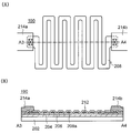
도 4는 반도체 장치에 적용될 수 있는 저항 소자(150)의 변형예를 도시한 것이다. 도 4의 (A)는 저항 소자(190)의 평면도이고, 도 4의 (B)는 도 4의 (A)를 A3-A4에서 절단한 단면도이다.Fig. 4 shows a modification of the
도 4에 도시된 저항 소자(190)는 산화물 반도체층(208a)의 형상이 도 1의 저항 소자(150)와 다르다. 구체적으로는 저항 소자(190)는 저항 소자(150)에 포함되는 섬 형상의 산화물 반도체층(208a) 대신에, 평면으로 볼 때 사행(蛇行)하는 형상을 가진 산화물 반도체층(208a)을 가진다. 이와 같은 형상의 산화물 반도체층(208a)은 섬 형상의 산화물 반도체층(208a)보다 캐리어가 흐르는 경로의 길이가 길다. 산화물 반도체층(208a)의 저항률과 산화물 반도체층(208a)의 캐리어가 흐르는 경로의 길이를 적절히 설정함으로써 임의의 저항률을 가지는 저항 소자로 할 수 있다.The
저항 소자(190)에 포함되는 산화물 반도체층(208a)의 캐리어가 흐르는 경로의 길이는 도시되어 있지 않은 트랜지스터(100)에 포함되는 산화물 반도체층(208b)의 캐리어가 흐르는 경로의 길이(채널 길이)보다 길게 하는 것이 바람직하다. 또한, 도 4에는 평면으로 볼 때 사행하는 형상을 가진 산화물 반도체층(208a)을 도시하였지만 형상은 이에 한정되지 않고 평면으로 볼 때 각부를 가진 직선 형상, 곡선 형상 등으로 함으로써 산화물 반도체층(208a)의 캐리어가 흐르는 경로의 길이를 조정하여도 좋다.The length of the path of the carrier of the
또한, 저항 소자(190)에 관해서는, 산화물 반도체층(208a)의 형상에 관한 사항을 제외하고는 저항 소자(150)에 대한 설명을 참조할 수 있다.With respect to the
<변형예 2>≪ Modification Example 2 &
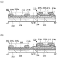
도 5의 (A)는 반도체 장치에 포함되는 트랜지스터 및 저항 소자의 변형예를 도시한 것이다. 도 5의 (A)에 도시된 저항 소자(160)는 기판(202) 위에 제공된 질화물 절연층(304)과, 질화물 절연층(304) 위에 접촉되는 산화물 반도체층(208a)과, 산화물 반도체층(208a)을 덮는 산화물 절연층(210)과, 산화물 절연층(210)에 제공된 콘택트 홀에서 산화물 반도체층(208a)과 전기적으로 접속된 전극층(214a) 및 전극층(214b)을 가진다. 저항 소자(160)에 포함되는 산화물 반도체층(208a)은 하면에 접촉하여 제공된 질화물 절연층(304)으로부터 수소가 공급됨으로써 저저항화된 산화물 반도체층이다.Fig. 5A shows a modification of the transistor and the resistance element included in the semiconductor device. 5A includes a
또한, 도 5의 (A)에 도시된 트랜지스터(110)는 기판(202) 위에 제공된 게이트 전극층(203)과, 게이트 전극층(203) 위의 질화물 절연층(304)과, 질화물 절연층(304) 위의 산화물 절연층(306)과, 산화물 절연층(306) 위의 산화물 반도체층(208b)과, 산화물 반도체층(208b) 위의 산화물 절연층(210)과, 산화물 절연층(210)에 제공된 콘택트 홀에서 산화물 반도체층(208b)과 전기적으로 접속된 전극층(214c) 및 전극층(214d)을 가진다.5A includes a
저항 소자(160) 및 트랜지스터(110)에는 공통적으로 질화물 절연층(304), 산화물 절연층(210)이 제공된다. 또한, 트랜지스터(110)에 있어서 질화물 절연층(304) 및 산화물 절연층(306)은 게이트 절연층에 상당한다. 도 5의 (A)에 도시된 반도체 장치에서는, 트랜지스터(110)의 게이트 절연층의 일부로서 기능하는 산화물 절연층(306)을 형성한 후에 이 산화물 절연층(306)을 선택적으로 에칭 처리함으로써, 산화물 반도체층(208a)이 형성되는 영역과 중첩되는 영역의 산화물 절연층(306)이 제거된다. 이로써 트랜지스터(110)의 게이트 절연층의 일부로서 기능하는 질화물 절연층(304)과 저항 소자(160)에 포함되는 산화물 반도체층(208a)이 접촉되는 구성으로 할 수 있다.The
또한, 저항 소자(160) 및 트랜지스터(110)에서는, 산화물 절연층(210) 위에 질화물 절연층(212)을 형성하고 블로킹층으로서 사용하여도 좋다.In the
또한, 도 5의 (A)는 산화물 반도체층(208a) 또는 산화물 반도체층(208b)에 도달되는 콘택트 홀을 형성하기 위한 산화물 절연층(210)의 에칭에 의하여 산화물 반도체층(208a) 및 산화물 반도체층(208b)의 일부가 오버 에칭된 경우를 예로 들어 도시한 것이다. 도 5의 (A)에 있어서, 산화물 반도체층(208a)에서 전극층(214a) 및 전극층(214b)과 접촉되는 영역의 막 두께는 산화물 절연층(210)과 접촉되는 영역의 막 두께보다 작다. 또한, 산화물 반도체층(208b)에서 전극층(214c) 및 전극층(214d)과 접촉되는 영역의 막 두께는 산화물 절연층(210)과 접촉되는 영역의 막 두께보다 작다. 다만, 산화물 반도체층(208a)에서 산화물 절연층(210)과 접촉되는 영역과 산화물 반도체층(208b)에서 산화물 절연층(210)과 접촉되는 영역은 막 두께가 같다. 또한, 산화물 반도체층(208a)에서 전극층(214a) 및 전극층(214b)과 접촉되는 영역과 산화물 반도체층(208b)에서 전극층(214c) 및 전극층(214d)과 접촉되는 영역은 막 두께가 같다.5A shows a state in which the
도 5의 (A)에 도시된 저항 소자(160)의 구성은, 산화물 반도체층(208a) 하면 전체에 접촉되는 질화물 절연층(304)으로부터 수소를 공급하여 산화물 반도체층(208a)을 전체에 걸쳐 저저항화시킬 수 있으며 도 1에 도시된 저항 소자(150)보다 마스크 수를 증가시킴이 없이 형성할 수 있다.The
<변형예 3>≪ Modification 3 &
도 5의 (B)는 반도체 장치에 포함되는 저항 소자 및 트랜지스터의 변형예를 도시한 것이다. 도 5의 (B)에 도시된 저항 소자(170)는 기판(202) 위에 제공된 질화물 절연층(304)과, 질화물 절연층(304) 위에 접촉되는 산화물 반도체층(208a)과, 산화물 반도체층(208a)을 덮는 질화물 절연층(212)과, 질화물 절연층(212)에 제공된 콘택트 홀에서 산화물 반도체층(208a)과 전기적으로 접속된 전극층(214a) 및 전극층(214b)을 가진다. 즉, 저항 소자(170)에 포함되는 산화물 반도체층(208a)은 하면에 접촉하여 제공된 질화물 절연층(304) 및 상면에 접촉하여 제공된 질화물 절연층(212) 양쪽으로부터 수소가 공급됨으로써 저저항화된 산화물 반도체층이다.5B shows a modification of the resistance element and the transistor included in the semiconductor device. The
또한, 도 5의 (B)에 도시된 트랜지스터(120)는 기판(202) 위에 제공된 게이트 전극층(203)과, 게이트 전극층(203) 위의 질화물 절연층(304)과, 질화물 절연층(304) 위의 산화물 절연층(306)과, 산화물 절연층(306) 위의 산화물 반도체층(208b)과, 산화물 반도체층(208b) 위의 산화물 절연층(210)과, 산화물 절연층(210) 위의 질화물 절연층(212)과, 질화물 절연층(212) 및 산화물 절연층(210)에 제공된 콘택트 홀에서 산화물 반도체층(208b)과 전기적으로 접속된 전극층(214c) 및 전극층(214d)을 가진다. 즉, 트랜지스터(120)는 트랜지스터(100)에 절연층(204)으로서 질화물 절연층(304)을 제공하고 절연층(206)으로서 산화물 절연층(306)을 제공한 구성이다.The
도 5의 (B)에 도시된 반도체 장치는 저항 소자(170)에 포함되는 산화물 반도체층(208a)에 상측과 하측의 양쪽 방향으로부터 수소가 공급됨으로써, 산화물 반도체층(208a)과 산화물 반도체층(208b)의 캐리어 밀도에 충분한 차가 생길 수 있다. 저항 소자에 요구되는 저항값에 따라서는 산화물 반도체층(208a)의 상측과 하측으로부터 수소를 공급하는 구성이 유효하다. 또한, 산화물 반도체층(208a)의 저항률에 따라서는 산화물 반도체층(208a)을 배선의 일부로서 사용하는 것도 가능하다.5B, hydrogen is supplied to the
<변형예 4><Modification 4>
도 6의 (A)는 반도체 장치에 포함되는 저항 소자 및 트랜지스터의 변형예를 도시한 것이다. 도 6의 (A)에 도시된 저항 소자(180)는 저항 소자(150)에 포함되는 산화물 반도체층(208a)을, 산화물 반도체층(207a)과 산화물 반도체층(209a)의 적층 구조로 한 경우의 예이다. 이 외의 구성은 저항 소자(150)와 같기 때문에 상술한 설명을 참작할 수 있다.6 (A) shows a modification of the resistance element and the transistor included in the semiconductor device. The
또한, 도 6의 (A)에 도시된 트랜지스터(130)는 트랜지스터(100)에 포함되는 산화물 반도체층(208b)을, 산화물 반도체층(207b)과 산화물 반도체층(209b)의 적층 구조로 한 경우의 예이다. 이 외의 구성은 트랜지스터(100)와 같기 때문에 상술한 설명을 참작할 수 있다.The
산화물 반도체층(207a) 및 산화물 반도체층(207b)(이하, 명세서에서는 산화물 반도체층(207)이라고도 표기함)과, 산화물 반도체층(209a) 및 산화물 반도체층(209b)(이하, 명세서에서는 산화물 반도체층(209)이라고도 표기함)에는 적어도 하나의 동일한 구성 원소를 가진 금속 산화물을 사용하는 것이 바람직하다. 또는, 산화물 반도체층(207)과 산화물 반도체층(209)의 구성 원소를 동일하게 하고 조성을 다르게 하여도 좋다.An
산화물 반도체층(207)이 In-M-Zn 산화물(M은 Al, Ga, Ge, Y, Zr, Sn, La, Ce, 또는 Hf)인 경우, In-M-Zn 산화물의 막을 형성하는 데 사용하는 스퍼터링 타깃의 금속 원소의 원자수비는 In≥M, Zn≥M을 만족시키는 것이 바람직하다. 이와 같은 스퍼터링 타깃의 금속 원소의 원자수비로서는 In:M:Zn=1:1:1, In:M:Zn=3:1:2가 바람직하다. 또한, 형성되는 산화물 반도체층(207)의 원자수비는 각각, 상기의 스퍼터링 타깃에 포함되는 금속 원소의 원자수비의 ±20%의 오차 변동을 포함한다.When the oxide semiconductor layer 207 is an In-M-Zn oxide (M is Al, Ga, Ge, Y, Zr, Sn, La, Ce or Hf) The atomic ratio of the metal element of the sputtering target preferably satisfies In? M, Zn? M. The atomic ratio of the metal element of the sputtering target is preferably In: M: Zn = 1: 1: 1 and In: M: Zn = 3: 1: 2. The atomic ratio of the oxide semiconductor layer 207 to be formed includes an error variation of ± 20% of the atomic ratio of the metal element contained in the sputtering target.
또한, 산화물 반도체층(207)이 In-M-Zn 산화물일 때, Zn과 O를 제외한 In과 M의 원자수비율은 바람직하게는 In을 25atomic% 이상, M을 75atomic% 미만, 더 바람직하게는 In을 34atomic% 이상, M을 66atomic% 미만으로 한다.When the oxide semiconductor layer 207 is an In-M-Zn oxide, the proportion of atoms of In and M excluding Zn and O is preferably 25 atomic% or more of In and less than 75 atomic% of M, In should be at least 34 atomic% and M should be less than 66 atomic%.
산화물 반도체층(207)의 에너지 갭은 2eV 이상, 바람직하게는 2.5eV 이상, 더 바람직하게는 3eV 이상이다. 이와 같이, 에너지 갭이 넓은 산화물 반도체를 사용함으로써, 트랜지스터의 오프 전류를 저감시킬 수 있다.The energy gap of the oxide semiconductor layer 207 is 2 eV or more, preferably 2.5 eV or more, and more preferably 3 eV or more. Thus, by using an oxide semiconductor having a wide energy gap, the off current of the transistor can be reduced.
산화물 반도체층(207)의 두께는 3㎚ 이상 200㎚ 이하, 바람직하게는 3㎚ 이상 100㎚ 이하, 더 바람직하게는 3㎚ 이상 50㎚ 이하로 한다.The thickness of the oxide semiconductor layer 207 is 3 nm or more and 200 nm or less, preferably 3 nm or more and 100 nm or less, and more preferably 3 nm or more and 50 nm or less.
산화물 반도체층(209)은 대표적으로는 In-Ga 산화물, In-Zn 산화물, In-M-Zn 산화물(M은 Al, Ga, Ge, Y, Zr, Sn, La, Ce, 또는 Hf)이고, 산화물 반도체층(207)보다 전도대 하단의 에너지가 진공 준위에 가까우며 대표적으로는 산화물 반도체층(209)의 전도대 하단의 에너지와 산화물 반도체층(207)의 전도대 하단의 에너지의 차가 0.05eV 이상, 0.07eV 이상, 0.1eV 이상, 또는 0.15eV 이상이고 2eV 이하, 1eV 이하, 0.5eV 이하, 또는 0.4eV 이하이다. 즉, 산화물 반도체층(209)의 전자 친화력과 산화물 반도체층(207)의 전자 친화력의 차가 0.05eV 이상, 0.07eV 이상, 0.1eV 이상, 또는 0.15eV 이상이고 2eV 이하, 1eV 이하, 0.5eV 이하, 또는 0.4eV 이하이다.The oxide semiconductor layer 209 is typically an In-Ga oxide, an In-Zn oxide, an In-M-Zn oxide (M is Al, Ga, Ge, Y, Zr, Sn, La, Ce, or Hf) The energy of the lower end of the conduction band is closer to the vacuum level than that of the oxide semiconductor layer 207. Typically, the difference between the energy of the lower conduction band of the oxide semiconductor layer 209 and the energy of the lower conduction band of the oxide semiconductor layer 207 is 0.05 eV or more, 0.1 eV or more, and 0.1 eV or more and 2 eV or less, 1 eV or less, 0.5 eV or less, or 0.4 eV or less. That is, the difference between the electron affinity of the oxide semiconductor layer 209 and the electron affinity of the oxide semiconductor layer 207 is 0.05 eV or more, 0.07 eV or more, 0.1 eV or more, or 0.15 eV or more and 2 eV or less, 1 eV or less, Or 0.4 eV or less.
산화물 반도체층(209)이 In보다 높은 원자수비로 상술한 원소 M을 가짐으로써 이하와 같은 효과가 나타날 수 있다. (1) 산화물 반도체층(209)의 에너지 갭 확장, (2) 산화물 반도체층(209)의 전자 친화력 감소, (3) 외부로부터의 불순물 차폐, 및 (4) 산화물 반도체층(207)보다 높은 절연성. 또한, 원소 M은 산소와의 결합력이 강한 금속 원소이기 때문에 In보다 높은 원자수비로 M을 가짐으로써 산소 결손이 생기기 어려워진다.The oxide semiconductor layer 209 has the above-described element M at a higher atomic ratio than In, so that the following effects can be obtained. (1) the energy gap expansion of the oxide semiconductor layer 209, (2) the reduction of the electron affinity of the oxide semiconductor layer 209, (3) the impurity shielding from the outside, and (4) . Further, since the element M is a metal element having a strong binding force with oxygen, the oxygen deficiency is hardly caused by having M at an atomic ratio higher than that of In.
산화물 반도체층(209)이 In-M-Zn 산화물일 때, Zn과 O를 제외한 In과 M의 원자수비율은 바람직하게는 In을 50atomic% 미만, M을 50atomic% 이상, 더 바람직하게는 In을 25atomic% 미만, M을 75atomic% 이상으로 한다.When the oxide semiconductor layer 209 is an In-M-Zn oxide, the proportion of atoms of In and M excluding Zn and O is preferably less than 50 atomic% and M is 50 atomic% or more, more preferably In Less than 25 atomic%, and M not less than 75 atomic%.
또한, 산화물 반도체층(207) 및 산화물 반도체층(209)이 In-M-Zn 산화물(M은 Al, Ga, Ge, Y, Zr, Sn, La, Ce, 또는 Hf)인 경우, 산화물 반도체층(209)에 포함되는 M의 원자수비는 산화물 반도체층(207)의 그것보다 크고 대표적으로는 산화물 반도체층(207)에 포함되는 상기 원자보다 그 원자수비가 1.5배 이상, 바람직하게는 2배 이상, 더 바람직하게는 3배 이상 높다.When the oxide semiconductor layer 207 and the oxide semiconductor layer 209 are In-M-Zn oxide (M is Al, Ga, Ge, Y, Zr, Sn, La, Ce, or Hf) The atomic ratio of M included in the oxide semiconductor layer 209 is larger than that of the oxide semiconductor layer 207 and representatively the atomic ratio of the atom contained in the oxide semiconductor layer 207 is 1.5 times or more, , More preferably three times or more.
또한, 산화물 반도체층(209)을 In:M:Zn=x1:y1:z1[원자수비], 산화물 반도체층(207)을 In:M:Zn=x2:y2:z2[원자수비]로 할 때 y1/x1는 y2/x2보다 크고 바람직하게는 y1/x1는 y2/x2의 1.5배 이상이다. 더 바람직하게는, y1/x1은 y2/x2의 2배 이상이고 더 바람직하게는 y1/x1은 y2/x2의 3배 이상이다. 이 때 산화물 반도체층에서 y2를 x2 이상으로 하면 상기 산화물 반도체층을 사용한 트랜지스터(130)에 안정된 전기 특성을 부여할 수 있으므로 바람직하다. 다만, y2가 x2의 3배 이상이면, 상기 산화물 반도체층을 사용한 트랜지스터(130)의 전계 효과 이동도가 저하되기 때문에 y2는 x2의 3배 미만인 것이 바람직하다.Further, the oxide semiconductor layer (209) In: M: Zn = x 1: y 1: the z 1 [atomic ratio], the oxide semiconductor layer (207) In: M: Zn = x 2: y 2: z 2 [ Atomic ratio], y 1 / x 1 is greater than y 2 / x 2 and preferably y 1 / x 1 is at least 1.5 times y 2 / x 2 . More preferably, y 1 / x 1 is at least two times y 2 / x 2 , and more preferably y 1 / x 1 is at least three times y 2 / x 2 . At this time, if y 2 is more than x 2 in the oxide semiconductor layer, stable electric characteristics can be imparted to the
산화물 반도체층(209)이 In-M-Zn 산화물일 때, In-M-Zn 산화물의 막을 형성하는 데 사용하는 스퍼터링 타깃의 금속 원소의 원자수비는 M>In, Zn>0.5×M, 또한 Zn>M을 만족시키는 것이 바람직하다. 스퍼터링 타깃의 금속 원소의 원자수비로서는 In:Ga:Zn=1:3:2, In:Ga:Zn=1:3:4, In:Ga:Zn=1:3:5, In:Ga:Zn=1:3:6, In:Ga:Zn=1:3:7, In:Ga:Zn=1:3:8, In:Ga:Zn=1:3:9, In:Ga:Zn=1:3:10, In:Ga:Zn=1:6:4, In:Ga:Zn=1:6:5, In:Ga:Zn=1:6:6, In:Ga:Zn=1:6:7, In:Ga:Zn=1:6:8, In:Ga:Zn=1:6:9, In:Ga:Zn=1:6:10이 바람직하다. 또한, 상기 스퍼터링 타깃을 사용하여 형성되는 산화물 반도체층(207) 및 산화물 반도체층(209)에 포함되는 금속 원소의 원자수비는 각각 상기 스퍼터링 타깃에 포함되는 금속 원소의 원자수비의 ±20%의 오차 변동을 포함한다.When the oxide semiconductor layer 209 is an In-M-Zn oxide, the atomic ratio of the metal element of the sputtering target used for forming the In-M-Zn oxide film is M> In, Zn> 0.5 x M, > M is satisfied. In: Ga: Zn = 1: 3: 2, In: Ga: Zn = 1: 3: 4, In: Ga: Zn = 1: 1: 3: 6, In: Ga: Zn = 1: 3: 7, In: Ga: Zn = 1: 3: 8, In: Ga: Zn = In: Ga: Zn = 1: 6: 4 In: Ga: Zn = 1: 6: 5 In: Ga: Zn = 1: 6: 6 In: Ga: Zn = 1: 6 Ga: Zn = 1: 6: 10, In: Ga: Zn = 1: 6: 8, In: Ga: Zn = 1: 6: The atomic ratio of the metal element contained in the oxide semiconductor layer 207 and the oxide semiconductor layer 209 formed using the sputtering target is set to be within a range of ± 20% of the atomic ratio of the metal element contained in the sputtering target .
또한 이에 한정되지 않고, 필요로 하는 트랜지스터의 반도체 특성 및 전기 특성(전계 효과 이동도, 문턱 전압 등)에 따라 적절한 조성의 것을 사용하면 좋다. 또한, 필요로 하는 트랜지스터의 반도체 특성을 얻기 위하여 산화물 반도체층(207)의 캐리어 밀도나 불순물 농도, 결함 밀도, 금속 원소와 산소의 원자수비, 원자간 거리, 밀도 등을 적절한 것으로 하는 것이 바람직하다.However, the present invention is not limited to this, and a suitable composition may be used depending on the semiconductor characteristics and electric characteristics (field effect mobility, threshold voltage, and the like) of the required transistor. In order to obtain the semiconductor characteristics of the required transistor, it is preferable that the carrier density, the impurity concentration, the defect density, the atomic number ratio of the metal element and the oxygen, the distance between atoms and the density of the oxide semiconductor layer 207 are appropriately set.
산화물 반도체층(209)은 나중에 산화물 절연층(210) 또는 질화물 절연층(212)을 형성할 때 산화물 반도체층(207)에 가해지는 대미지를 완화시키는 막으로서도 기능한다. 산화물 반도체층(209)의 두께는 3㎚ 이상 100㎚ 이하, 바람직하게는 3㎚ 이상 50㎚ 이하로 한다.The oxide semiconductor layer 209 also functions as a film for alleviating the damage to the oxide semiconductor layer 207 when the
트랜지스터(130)에 포함되는 산화물 반도체층(207b)에 제 14족 원소 중 하나인 실리콘이나 탄소가 포함되면, 산화물 반도체층(207b)에서 산소 결손이 증가되어 n형화된다. 그러므로, 산화물 반도체층(207b)의 실리콘이나 탄소의 농도, 또는 산화물 반도체층(209b)과 산화물 반도체층(207b)의 계면 근방에서의 실리콘이나 탄소의 농도(이차 이온 질량 분석법으로 얻어지는 농도)를 2×10¹⁸atoms/㎤ 이하, 바람직하게는 2×10¹⁷atoms/㎤ 이하로 한다.When the
또한 산화물 반도체층(207b)의, 이차 이온 질량 분석법으로 얻어지는 알칼리 금속 또는 알칼리 토금속의 농도를 1×10¹⁸atoms/㎤ 이하, 바람직하게는 2×10¹⁶atoms/㎤ 이하로 한다. 알칼리 금속 및 알칼리 토금속은 산화물 반도체와 결합되면 캐리어를 생성시킬 수 있고 이로 인하여 트랜지스터의 오프 전류가 증대되는 경우가 있다. 그러므로, 산화물 반도체층(207b)의 알칼리 금속 또는 알칼리 토금속의 농도는 저감시키는 것이 바람직하다.Also, the concentration of the alkali metal or alkaline earth metal obtained by the secondary ion mass spectrometry of the
또한, 산화물 반도체층(207b)에 질소가 포함되어 있으면 캐리어인 전자가 생기고 캐리어 밀도가 증가되어 n형화되기 쉽다. 이 때문에, 질소가 포함된 산화물 반도체층을 사용한 트랜지스터는 노멀리 온 특성을 가지기 쉽다. 따라서, 상기 산화물 반도체층에서 질소는 가능한 한 저감되는 것이 바람직하고 예를 들어 이차 이온 질량 분석법으로 얻어지는 질소 농도는 5×10¹⁸atoms/㎤ 이하로 하는 것이 바람직하다.In addition, if nitrogen is contained in the
또한, 도 6의 (A)에 도시된 트랜지스터(130)에는, 게이트 전극층(203) 측에 위치하고 캐리어의 주된 이동 경로가 되는 산화물 반도체층(207)과 산화물 절연층(210) 사이에 산화물 반도체층(209)이 제공된다. 그러므로, 산화물 반도체층(209)과 산화물 절연층(210) 사이에서 불순물 및 결함에 기인하여 트랩 준위가 형성되더라도 이 트랩 준위와 산화물 반도체층(207) 사이에는 거리가 있다. 이 결과 산화물 반도체층(207)을 흐르는 전자가 트랩 준위에 포획되기 어렵기 때문에 트랜지스터(130)의 온 전류를 증대시킬 수 있으며 전계 효과 이동도를 높일 수 있다. 또한, 트랩 준위에 전자가 포획되면, 이 전자가 음의 고정 전하가 됨으로써 트랜지스터(130)의 문턱 전압이 변동된다. 그러나, 산화물 반도체층(207)과 트랩 준위 사이에 거리가 있음으로써 트랩 준위에서의 전자의 포획을 저감시킬 수 있고, 문턱 전압의 변동을 저감시킬 수 있다.In the
또한, 산화물 반도체층(207) 및 산화물 반도체층(209)은 각 층을 단순히 적층시키는 것이 아니라 연속 접합(여기서는 특히 전도대 하단의 에너지가 각 층간에서 연속적으로 변화되는 구조를 말함)이 형성되도록 제작한다. 즉, 각 층의 계면에 트랩 중심이나 재결합 중심과 같은 결함 준위를 형성하는 불순물이 존재하지 않는 적층 구조로 한다. 만약에 적층된 산화물 반도체층(207) 및 산화물 반도체층(209) 사이에 불순물이 혼재하고 있으면 에너지 밴드의 연속성이 저하되어 계면에서 캐리어가 포획되거나 또는 재결합하여 소멸된다.The oxide semiconductor layer 207 and the oxide semiconductor layer 209 are formed so as not to simply laminate the respective layers but to form a continuous junction (in this case, in particular, a structure in which energy at the lower end of the conduction path is continuously changed between layers) . That is, a layered structure in which no impurity that forms a defect level such as a trap center or a recombination center is present at the interface of each layer. If impurities are mixed between the stacked oxide semiconductor layer 207 and the oxide semiconductor layer 209, the continuity of the energy band is lowered, so that the carriers are trapped at the interface or are recombined to disappear.
연속 접합을 형성하기 위해서는 로드록실(load lock chamber)을 구비한 멀티 챔버 방식 성막 장치(스퍼터링 장치)를 사용하여 각 층을 대기에 노출시키지 않고 연속적으로 적층할 필요가 있다. 스퍼터링 장치의 각 챔버는, 산화물 반도체층에 있어서 불순물로서 기능하는 물 등을 가능한 한 제거하기 위하여 크라이오 펌프와 같은 흡착식 진공 배기 펌프를 사용하여 고진공 배기(5×10⁻⁷Pa 이상 1×10⁻⁴Pa 이하 정도까지)하는 것이 바람직하다. 또는 터보 분자 펌프와 콜드 트랩을 조합하여 배기계로부터 챔버 내에 기체, 특히 탄소 또는 수소를 포함하는 기체가 역류되지 않도록 하는 것이 바람직하다.In order to form a continuous junction, it is necessary to successively laminate each layer without exposing each layer to the atmosphere by using a multi-chamber type film forming apparatus (sputtering apparatus) provided with a load lock chamber. Each chamber of the sputtering apparatus, and oxide in a semiconductor layer using the adsorption-type vacuum exhaust pump such as a cryopump for removing possible water and the like, which functions as an impurity vacuum exhaust (5 × 10 -7 or
여기서, 트랜지스터(130)에 포함되는 적층 구조의 밴드 구조에 대하여 도 6의 (B)를 사용하여 설명한다.Here, the band structure of the laminated structure included in the
도 6의 (B)는 트랜지스터(130)에 포함되는 밴드 구조의 일부를 모식적으로 도시한 것이다. 여기서는 절연층(206) 및 산화물 절연층(210)으로서 산화 실리콘층을 제공한 경우에 대하여 설명한다. 또한, 도 6의 (B)에서 EcI1은 절연층(206)으로서 사용하는 산화 실리콘층의 전도대 하단의 에너지를 나타내고, EcS1은 산화물 반도체층(207b)의 전도대 하단의 에너지를 나타내고, EcS2는 산화물 반도체층(209b)의 전도대 하단의 에너지를 나타내고, EcI2는 산화물 절연층(210)으로서 사용하는 산화 실리콘층의 전도대 하단의 에너지를 나타낸다.FIG. 6B schematically shows a part of the band structure included in the
도 6의 (B)에 나타낸 바와 같이, 산화물 반도체층(207b) 및 산화물 반도체층(209b)에서, 전도대 하단의 에너지는 장벽이 없이 완만하게 변화한다. 연속적으로 변화한다고 바꿔 말할 수도 있다. 이것은 산화물 반도체층(207b)과 산화물 반도체층(209b)이 공통의 원소를 포함하고 산화물 반도체층(207b)과 산화물 반도체층(209b) 사이에서 산소가 상호로 이동함으로써 혼합층이 형성되기 때문이라고 할 수 있다.As shown in Fig. 6B, in the
도 6의 (B)로부터, 산화물 반도체층(208b)에서 산화물 반도체층(207b)이 웰(well; 우물)이 되고, 산화물 반도체층(208b)을 사용한 트랜지스터에서 채널 영역이 산화물 반도체층(207)에 형성되는 것을 알 수 있다. 또한, 산화물 반도체층(208b)은 전도대 하단의 에너지가 연속적으로 변화되기 때문에, 산화물 반도체층(207b)과 산화물 반도체층(209b)이 연속 접합되어 있다고 할 수도 있다.The
또한, 도 6의 (B)에 나타낸 바와 같이 산화물 반도체층(209b)과 산화물 절연층(210)의 계면 근방에서는 산화물 절연층(210)의 구성 원소인 실리콘 또는 탄소 등 불순물이나 결함에 기인하여 트랩 준위가 형성될 수 있지만, 산화물 반도체층(209)을 제공함으로써 산화물 반도체층(207b)과 상기 트랩 준위를 떨어지게 할 수 있다. 다만, EcS1과 EcS2 사이의 에너지 차가 작은 경우, 산화물 반도체층(207b)의 전자가 상기 에너지 차를 넘어 트랩 준위에 도달되는 경우가 있다. 트랩 준위에 전자가 포획됨으로써, 산화물 절연층 계면 또는 그 근방에 음의 고정 전하가 발생되고 트랜지스터의 문턱 전압은 양 방향으로 시프트된다. 따라서, EcS1과 EcS2 사이의 에너지 차를 0.1eV 이상, 바람직하게는 0.15eV 이상으로 하면, 트랜지스터의 문턱 전압의 변동이 저감되어, 전기 특성이 안정되기 때문에 바람직하다.6 (B), due to impurities or defects such as silicon or carbon which is a constituent element of the
또한, 도 6에는 도 1에 도시된 저항 소자(150) 및 트랜지스터(100)에 포함되는 산화물 반도체층을 적층 구조로 하는 경우를 예시하였지만 본 실시형태는 이에 한정되지 않고 도 4 또는 도 5에 도시된 구성의 반도체 장치에 포함되는 산화물 반도체층을 적층 구조로 하여도 좋다.6 illustrates a case where the oxide semiconductor layers included in the
또한, 본 실시형태에서 기재된 반도체 장치의 구성예는 각각 부분적으로 구성이 다르지만 본 발명의 일 형태는 특별히 한정되지 않고 다양한 조합이 가능하다. 예를 들어, 도 6에 도시된 적층 구조를 가진 산화물 반도체층에서 전극층과 접촉되는 영역은 산화물 절연층 또는 질화물 절연층과 접촉되는 영역보다 막 두께가 작아도 좋다.Although the constitution examples of the semiconductor device described in this embodiment each have a partially different constitution, one embodiment of the present invention is not particularly limited and various combinations are possible. For example, in the oxide semiconductor layer having the stacked structure shown in FIG. 6, the region which is in contact with the electrode layer may be smaller in film thickness than the region in contact with the oxide insulating layer or the nitride insulating layer.
본 실시형태에 기재된 반도체 장치는 산화물 반도체층을 포함한 저항 소자와 산화물 반도체층을 포함한 트랜지스터를 동일한 기판 위에 가지고, 각각의 산화물 반도체층은 상면 또는 하면에 접촉되는 절연층으로 막 내의 불순물 농도가 제어되어, 상이한 캐리어 밀도를 가진다. 구체적으로는 저항 소자에 포함되는 산화물 반도체층은 상면 또는 하면 전체에 접촉되는 질화물 절연층에 의하여 수소가 공급됨으로써 저저항화된 캐리어 밀도가 높은 산화물 반도체층이다. 또한, 트랜지스터에 포함되는 산화물 반도체층은 적어도 상면에 접촉되는 산화물 절연층에 의하여 산소가 공급됨으로써 산소 결손이 저감되어 고저항화된 캐리어 밀도가 낮은 산화물 반도체층이다.The semiconductor device according to the present embodiment has a resistive element including an oxide semiconductor layer and a transistor including an oxide semiconductor layer on the same substrate and each oxide semiconductor layer is controlled to have an impurity concentration in the film by an insulating layer contacting the upper or lower surface , And have different carrier densities. Specifically, the oxide semiconductor layer included in the resistance element is an oxide semiconductor layer having a low carrier density by supplying hydrogen by the nitride insulating layer contacting the entire upper surface or the lower surface. In addition, the oxide semiconductor layer included in the transistor is an oxide semiconductor layer with reduced oxygen deficiency due to supply of oxygen by at least an oxide insulating layer in contact with the upper surface thereof, resulting in a high resistivity carrier density.
본 실시형태에 기재된 구성이나 방법 등은 다른 실시형태에 기재된 구성이나 방법 등과 적절히 조합하여 사용할 수 있다.The constitution, the method, and the like described in this embodiment can be appropriately combined with the constitution, the method, and the like described in the other embodiments.
(실시형태 2)(Embodiment 2)
본 실시형태에서는 실시형태 1에 기재된 트랜지스터 및 저항 소자에 적용될 수 있는 산화물 반도체층의 일례에 대하여 설명한다.In this embodiment mode, an example of an oxide semiconductor layer that can be applied to the transistor and the resistance element described in
<산화물 반도체층의 결정성>≪ Crystallinity of oxide semiconductor layer >
이하에서는 산화물 반도체층의 구조에 대하여 설명한다.Hereinafter, the structure of the oxide semiconductor layer will be described.
산화물 반도체층은 비단결정 산화물 반도체층과 단결정 산화물 반도체층으로 대별된다. 비단결정 산화물 반도체층이란, CAAC-OS(C-Axis Aligned Crystalline Oxide Semiconductor)막, 다결정 산화물 반도체층, 미결정 산화물 반도체층, 비정질 산화물 반도체층 등을 말한다.The oxide semiconductor layer is roughly divided into a non-single crystal oxide semiconductor layer and a single crystal oxide semiconductor layer. The non-single crystal oxide semiconductor layer refers to a CAAC-OS (C-Axis Aligned Crystalline Oxide Semiconductor) film, a polycrystalline oxide semiconductor layer, a microcrystalline oxide semiconductor layer, an amorphous oxide semiconductor layer or the like.
우선, CAAC-OS막에 대하여 설명한다.First, the CAAC-OS film will be described.
CAAC-OS막은 복수의 결정부를 가지는 산화물 반도체층 중 하나이며 결정부의 대부분은 한 변이 100㎚ 미만인 입방체 내에 들어가는 크기이다. 따라서, CAAC-OS막에 포함되는 결정부는 한 변이 10㎚ 미만, 5㎚ 미만, 또는 3㎚ 미만인 입방체 내에 들어가는 크기인 경우도 포함된다.The CAAC-OS film is one of the oxide semiconductor layers having a plurality of crystal portions, and most of the crystal portions are large enough to be contained in a cube having one side of less than 100 nm. Therefore, the crystal part included in the CAAC-OS film also includes a case where the size is such that one side falls within a cube of less than 10 nm, less than 5 nm, or less than 3 nm.
CAAC-OS막을 투과형 전자 현미경(TEM: Transmission Electron Microscope)에 의하여 관찰하면, 명확한 결정부들끼리의 경계 즉, 결정 입계(그레인 바운더리라고도 함)는 확인되지 않는다. 따라서, CAAC-OS막은 결정 입계에 기인하는 전자 이동도의 저하가 일어나기 어렵다고 할 수 있다.When the CAAC-OS film is observed by a transmission electron microscope (TEM), the boundaries between definite crystal portions, that is, crystal grain boundaries (also referred to as grain boundaries) are not confirmed. Therefore, it can be said that the CAAC-OS film is less likely to lower the electron mobility due to the crystal grain boundaries.
CAAC-OS막을 시료면에 대략 평행한 방향으로부터 TEM에 의하여 관찰(단면 TEM 관찰)하면, 결정부에서 금속 원자가 층상으로 배열되어 있는 것을 확인할 수 있다. 금속 원자의 각 층은 CAAC-OS막이 형성되는 면(피형성면이라고도 함) 또는 CAAC-OS막의 상면의 요철이 반영된 형상이며 CAAC-OS막의 피형성면 또는 상면에 평행하게 배열된다.When the CAAC-OS film is observed by TEM (cross-sectional TEM observation) from the direction substantially parallel to the sample surface, it can be confirmed that the metal atoms are arranged in layers in the crystal part. Each layer of the metal atoms has a shape reflecting the concavities and convexities of the upper surface of the CAAC-OS film (also referred to as the surface to be formed) on which the CAAC-OS film is formed and is arranged parallel to the surface to be formed or the upper surface of the CAAC-OS film.
또한, 본 명세서에 있어서, "평행"이란, 2개의 직선이 -10° 이상 10° 이하의 각도로 배치된 상태를 말한다. 따라서, -5° 이상 5° 이하의 경우도 그 범주에 포함된다. 또한, "수직"이란, 2개의 직선이 80° 이상 100° 이하의 각도로 배치된 상태를 말한다. 따라서, 85° 이상 95° 이하의 경우도 그 범주에 포함된다.In this specification, "parallel" refers to a state in which two straight lines are arranged at an angle of -10 DEG to 10 DEG. Therefore, the range of -5 DEG to 5 DEG is also included in the category. The term "vertical" refers to a state in which two straight lines are arranged at angles of 80 DEG to 100 DEG. Therefore, the range of 85 degrees or more and 95 degrees or less is included in the category.
한편, CAAC-OS막을 시료면에 대략 수직인 방향으로부터 TEM에 의하여 관찰(평면 TEM 관찰)하면, 결정부에서 금속 원자가 삼각형 또는 육각형으로 배열되어 있는 것을 확인할 수 있다. 그러나, 상이한 결정부들간에서 금속 원자의 배열에는 규칙성은 없다.On the other hand, when the CAAC-OS film is observed by TEM (plane TEM observation) from a direction substantially perpendicular to the sample surface, it can be confirmed that the metal atoms are arranged in a triangular or hexagonal shape in the crystal part. However, there is no regularity in the arrangement of the metal atoms between the different crystal portions.
단면 TEM 관찰 및 평면 TEM 관찰로부터, CAAC-OS막의 결정부가 배향성을 가짐을 알 수 있다.From the cross-sectional TEM observation and the planar TEM observation, it can be seen that the CAAC-OS film has a crystal addition orientation.
CAAC-OS막에 대하여 X선 회절(XRD: X-Ray Diffraction) 장치를 사용하여 구조 해석을 수행하면, 예를 들어, InGaZnO4의 결정을 가진 CAAC-OS막의 out-of-plane법에 의한 해석에서는, 회절각(2θ)이 31° 근방일 때 피크가 나타나는 경우가 있다. 이 피크는, InGaZnO4의 결정의 (009)면에 귀속되기 때문에, CAAC-OS막의 결정이 c축 배향성을 가지고, c축이 피형성면 또는 상면에 대략 수직인 방향으로 배향되는 것을 확인할 수 있다.When the structure analysis is performed using the X-ray diffraction (XRD) apparatus for the CAAC-OS film, for example, the out-of-plane analysis of the CAAC-OS film having the crystal of InGaZnO 4 A peak may appear when the diffraction angle 2 [theta] is in the vicinity of 31 [deg.]. Since this peak belongs to the (009) plane of the crystal of InGaZnO 4 , it can be confirmed that the crystal of the CAAC-OS film has a c-axis orientation and the c-axis is oriented in a direction substantially perpendicular to the surface to be formed or the top surface .
한편, CAAC-OS막에 대하여 c축에 대략 수직인 방향으로부터 X선을 입사시키는 in-plane법에 의한 해석을 수행하면, 2θ가 56° 근방일 때 피크가 나타나는 경우가 있다. 이 피크는 InGaZnO4의 결정의 (110)면에 귀속된다. InGaZnO4의 단결정 산화물 반도체층의 경우에는, 2θ를 56° 근방에 고정시키고, 시료면의 법선 벡터를 축(φ축)으로 하여 시료를 회전시키면서 분석(φ 스캔)을 수행하면, (110)면과 등가인 결정면에 귀속되는 6개의 피크가 관찰된다. 한편, CAAC-OS막의 경우에는, 2θ를 56° 근방에 고정시키고 φ 스캔을 수행하여도 명료한 피크가 나타나지 않는다.On the other hand, when the in-plane analysis is performed on the CAAC-OS film in which an X-ray is incident from a direction substantially perpendicular to the c-axis, a peak may appear when 2θ is in the vicinity of 56 °. This peak belongs to the (110) plane of the crystal of InGaZnO 4 . In the case of a single crystal oxide semiconductor layer of InGaZnO 4 , when the analysis is performed while the sample is rotated (φ scan) while the 2θ is fixed near 56 ° and the normal vector of the sample surface is the axis (φ axis) Six peaks attributed to the crystal planes equivalent to < RTI ID = 0.0 > On the other hand, in the case of the CAAC-OS film, even when 2? Is fixed in the vicinity of 56 占 and φ scan is performed, no distinct peak appears.
상술한 것으로부터, CAAC-OS막에서는, 상이한 결정부들간에서 a축 및 b축의 배향이 불규칙하지만, c축 배향성을 가지며 c축이 피형성면 또는 상면의 법선 벡터에 평행한 방향으로 배향되는 것을 알 수 있다. 따라서, 상술한 단면 TEM 관찰로 확인된 층상으로 배열된 금속 원자의 각 층은, 결정의 a-b면에 평행한 면이다.As described above, in the CAAC-OS film, although the orientation of the a-axis and the b-axis is irregular among the different crystal portions, the orientation of the c-axis is oriented in a direction parallel to the normal vector of the surface to be imaged or the top surface Able to know. Thus, each layer of metal atoms arranged in layers identified by the above-mentioned cross-sectional TEM observation is a plane parallel to the a-b plane of the crystal.
또한, 결정부는 CAAC-OS막을 형성하였을 때, 또는 가열 처리 등의 결정화 처리를 수행하였을 때 형성된다. 상술한 바와 같이, 결정의 c축은 CAAC-OS막의 피형성면 또는 상면의 법선 벡터에 평행한 방향으로 배향된다. 따라서, 예를 들어 CAAC-OS막의 형상을 에칭 등에 의하여 변화시킨 경우, 결정의 c축이 CAAC-OS막의 피형성면 또는 상면의 법선 벡터에 평행하게 배향되지 않을 수도 있다.The crystallizing portion is formed when the CAAC-OS film is formed, or when a crystallization process such as heat treatment is performed. As described above, the c-axis of the crystal is oriented parallel to the normal vector on the surface to be formed or the upper surface of the CAAC-OS film. Therefore, for example, when the shape of the CAAC-OS film is changed by etching or the like, the c-axis of the crystal may not be oriented parallel to the normal vector of the surface or top surface of the CAAC-OS film.
또한, CAAC-OS막 내의 결정화도는 균일하지 않아도 된다. 예를 들어, CAAC-OS막의 결정부가 CAAC-OS막의 상면 근방으로부터의 결정 성장에 의하여 형성되는 경우에는, 상면 근방의 영역은 피형성면 근방의 영역보다 결정화도가 높게 될 수 있다. 또한, CAAC-OS막에 불순물을 첨가하는 경우에는, 불순물이 첨가된 영역의 결정화도가 변화되어, 부분적으로 결정화도가 다른 영역이 형성될 수도 있다.In addition, the degree of crystallization in the CAAC-OS film need not be uniform. For example, when the crystal portion of the CAAC-OS film is formed by crystal growth from the vicinity of the top surface of the CAAC-OS film, the region near the top surface may have a higher degree of crystallinity than the region near the surface to be coated. In addition, when an impurity is added to the CAAC-OS film, the degree of crystallinity of the region to which the impurity is added may be changed, so that a region having a partially different degree of crystallinity may be formed.
또한, InGaZnO4의 결정을 가진 CAAC-OS막의 out-of-plane법에 의한 해석에서는, 2θ가 31° 근방일 때 나타나는 피크에 더하여, 2θ가 36° 근방일 때도 피크가 나타나는 경우가 있다. 2θ가 36° 근방일 때 나타나는 피크는 CAAC-OS막 내의 일부에, c축 배향성을 가지지 않는 결정이 포함되는 것을 가리킨다. CAAC-OS막은 2θ가 31° 근방일 때 피크가 나타나고, 2θ가 36° 근방일 때 피크가 나타나지 않는 것이 바람직하다.In the analysis of the CAAC-OS film having crystals of InGaZnO 4 by the out-of-plane method, in addition to the peak appearing when 2θ is in the vicinity of 31 °, a peak may appear even when 2θ is in the vicinity of 36 °. The peak appearing when 2? Is in the vicinity of 36 ° indicates that crystals having no c-axis orientation are included in a part of the CAAC-OS film. It is preferable that the CAAC-OS film exhibits a peak when 2? Is in the vicinity of 31 占 and a peak does not appear when 2? Is in the vicinity of 36 占.
또한, 본 명세서에 있어서, 삼방정 또는 능면체정(rhombohedral crystal)은 육방정계에 포함된다.Also, in the present specification, a rhombohedral crystal is contained in a hexagonal system.
CAAC-OS막은 불순물 농도가 낮은 산화물 반도체층이다. 불순물은 수소, 탄소, 실리콘, 전이 금속 원소 등, 산화물 반도체층의 주성분 이외의 원소이다. 특히 실리콘 등, 산화물 반도체층을 구성하는 금속 원소보다 산소와의 결합력이 강한 원소는, 산화물 반도체층으로부터 산소를 빼앗음으로써 산화물 반도체층의 원자 배열을 흐트러지게 하여 결정성을 저하시키는 요인이 된다. 또한, 철이나 니켈 등의 중금속, 아르곤, 이산화탄소 등은, 원자 반경(또는 분자 반경)이 크기 때문에 산화물 반도체층 내부에 포함되면 산화물 반도체층의 원자 배열을 흐트러지게 하여 결정성을 저하시키는 요인이 된다. 또한, 산화물 반도체층에 포함되는 불순물은 캐리어 트랩이나 캐리어 발생원이 되는 경우가 있다.The CAAC-OS film is an oxide semiconductor layer with a low impurity concentration. The impurity is an element other than the main component of the oxide semiconductor layer, such as hydrogen, carbon, silicon, or a transition metal element. Particularly, an element having stronger bonding force with oxygen than a metal element constituting the oxide semiconductor layer, such as silicon, dislodges the atomic arrangement of the oxide semiconductor layer by depriving oxygen from the oxide semiconductor layer, thereby deteriorating crystallinity. Further, heavy metals such as iron and nickel, argon, carbon dioxide and the like have a large atomic radius (or a large molecule radius), and when they are contained in the oxide semiconductor layer, the atomic arrangement of the oxide semiconductor layer is disturbed, . In addition, the impurity contained in the oxide semiconductor layer may be a carrier trap or a carrier generation source.
또한, CAAC-OS막은 결함 준위 밀도가 낮은 산화물 반도체층이다.The CAAC-OS film is an oxide semiconductor layer with a low defect level density.
또한 CAAC-OS막을 사용한 트랜지스터는 가시광이나 자외광의 조사로 인한 전기 특성의 변동이 작다.In addition, the transistor using the CAAC-OS film has a small variation in electric characteristics due to irradiation of visible light and ultraviolet light.
다음에, 미결정 산화물 반도체층에 대하여 설명한다.Next, the microcrystalline oxide semiconductor layer will be described.
미결정 산화물 반도체층은 TEM에 의한 관찰상에서 결정부가 명확히 확인되지 않는 경우가 있다. 미결정 산화물 반도체층에 포함되는 결정부는 크기가 1㎚ 이상 100㎚ 이하, 또는 1㎚ 이상 10㎚ 이하인 경우가 많다. 특히, 1㎚ 이상 10㎚ 이하, 또는 1㎚ 이상 3㎚ 이하의 미결정인 나노 결정(nc: nanocrystal)을 가진 산화물 반도체층을 nc-OS(nanocrystalline Oxide Semiconductor)막이라고 부른다. 또한, nc-OS막은 예를 들어, TEM에 의한 관찰상에서는 결정 입계가 명확히 확인되지 않는 경우가 있다.Crystalline portions of the microcrystalline oxide semiconductor layer on the observation by TEM may not be clearly confirmed. The crystal portion included in the microcrystalline oxide semiconductor layer has a size of 1 nm or more and 100 nm or less, or 1 nm or more and 10 nm or less in many cases. In particular, an oxide semiconductor layer having a microcrystalline nc (nanocrystal) of 1 nm or more and 10 nm or less or 1 nm or more and 3 nm or less is called a nc-OS (nanocrystalline oxide semiconductor) film. Further, in the nc-OS film, for example, the grain boundary can not be clearly confirmed on observation by TEM.
nc-OS막은 미소 영역(예를 들어 1㎚ 이상 10㎚ 이하의 영역, 특히 1㎚ 이상 3㎚ 이하의 영역)에서 원자 배열에 주기성이 있다. 또한, nc-OS막은 상이한 결정부들간에서 결정 방위에 규칙성이 없다. 그러므로, 막 전체에서 배향성이 확인되지 않는다. 따라서, nc-OS막은 분석 방법에 따라서는 비정질 산화물 반도체층과 구별할 수 없는 경우가 있다. 예를 들어 결정부보다 직경이 큰 X선을 사용하는 XRD 장치를 사용하여 nc-OS막의 구조를 해석하면, out-of-plane법에 의한 해석에서는 결정면을 가리키는 피크가 검출되지 않는다. 또한, nc-OS막에 대하여, 결정부보다 직경이 큰 (예를 들어 50㎚ 이상) 전자선을 사용하는 전자선 회절(제한 시야 전자선 회절이라고도 함)을 수행하면, 할로 패턴(halo pattern)과 같은 회절 패턴이 관측된다. 한편, nc-OS막에 대하여, 프로브 직경이 결정부의 크기와 가깝거나 작은(예를 들어 1㎚ 이상 30㎚ 이하) 전자선을 사용한 전자선 회절(나노 빔 전자선 회절이라고도 함)을 수행하면, 스폿이 관측된다. 또한, nc-OS막에 대하여 나노 빔 전자선 회절을 수행하면, 휘도가 높은 원형(환(環)형) 영역이 관측되는 경우가 있다. 또한, nc-OS막에 대하여 나노 빔 전자선 회절을 수행하면, 환형 영역 내에 복수의 스폿이 관측되는 경우가 있다.The nc-OS film has periodicity in the atomic arrangement in a minute region (for example, a region of 1 nm or more and 10 nm or less, particularly a region of 1 nm or more and 3 nm or less). In addition, the nc-OS film has no regularity in crystal orientation between different crystal portions. Therefore, the orientation is not confirmed throughout the film. Therefore, the nc-OS film may not be distinguishable from the amorphous oxide semiconductor layer depending on the analysis method. For example, when the structure of the nc-OS film is analyzed by using an XRD apparatus using an X-ray having a diameter larger than that of the crystal portion, a peak pointing to the crystal face is not detected in the analysis by the out-of-plane method. Further, when electron beam diffraction (also referred to as limited viewing electron beam diffraction) using an electron beam having a larger diameter (for example, 50 nm or more) than the crystal part is performed on the nc-OS film, diffraction such as a halo pattern Pattern is observed. On the other hand, when the nc-OS film is subjected to electron beam diffraction (also referred to as nano-beam electron beam diffraction) using an electron beam whose probe diameter is close to or smaller than the size of the crystal portion (for example, 1 nm to 30 nm) do. In addition, when nano-beam electron diffraction is performed on the nc-OS film, a circular (ring) region having a high luminance may be observed. Further, when nano-beam electron diffraction is performed on the nc-OS film, a plurality of spots may be observed in the annular region.
nc-OS막은 비정질 산화물 반도체층보다 규칙성이 높은 산화물 반도체층이다. 그러므로, nc-OS막은 비정질 산화물 반도체층보다 결함 준위 밀도가 낮다. 다만, nc-OS막은 상이한 결정부들간에서 결정 방위에 규칙성이 없다. 따라서, nc-OS막은 CAAC-OS막보다 결함 준위 밀도가 높다.The nc-OS film is an oxide semiconductor layer having higher regularity than the amorphous oxide semiconductor layer. Therefore, the nc-OS film has a lower defect level density than the amorphous oxide semiconductor layer. However, the nc-OS film has no regularity in crystal orientation between different crystal portions. Therefore, the nc-OS film has a higher defect level density than the CAAC-OS film.
또한, 산화물 반도체층은, 예를 들어 비정질 산화물 반도체층, 미결정 산화물 반도체층, CAAC-OS막 중 2개 이상을 가진 적층막이어도 좋다.The oxide semiconductor layer may be a laminated film having two or more of, for example, an amorphous oxide semiconductor layer, a microcrystalline oxide semiconductor layer, and a CAAC-OS film.
<CAAC-OS막의 형성 방법><Method of forming CAAC-OS film>
CAAC-OS막은 예를 들어, 다결정의 산화물 반도체 스퍼터링용 타깃을 사용하여 스퍼터링법으로 형성한다. 상기 스퍼터링용 타깃에 이온이 충돌되면, 스퍼터링용 타깃에 포함되는 결정 영역이, a-b면으로부터 벽개(劈開)되고 a-b면에 평행한 면을 가진 평판 형상 또는 펠릿(pellet) 형상의 스퍼터링 입자로서 박리되는 경우가 있다. 이 경우, 상기 평판 형상의 스퍼터링 입자가 결정 상태를 유지한 채 기판에 도달됨으로써, CAAC-OS막을 형성할 수 있다.The CAAC-OS film is formed by, for example, a sputtering method using a polycrystalline oxide semiconductor target for sputtering. When ions collide with the sputtering target, the crystal region included in the target for sputtering is cleaved from the ab plane and is peeled off as a flat plate-like or pellet-shaped sputtering particle having a plane parallel to the ab plane There is a case. In this case, the flat sputtering particles reach the substrate while maintaining the crystal state, so that the CAAC-OS film can be formed.
평판 형상의 스퍼터링 입자는 예를 들어, a-b면에 평행한 면의 원 상당 직경이 3㎚ 이상 10㎚ 이하, 두께(a-b면에 수직인 방향의 길이)가 0.7㎚ 이상 1㎚ 미만이다. 또한, 평판 형상의 스퍼터링 입자는 a-b면에 평행한 면이 정삼각형 또는 정육각형이어도 좋다. 여기서 면의 원 상당 직경이란, 면의 면적과 같은 정원(正圓)의 직경을 말한다.For example, the plane-parallel sputtering particles have a circle-equivalent diameter of 3 nm or more and 10 nm or less and a thickness (length in the direction perpendicular to the a-b plane) of 0.7 nm or more and less than 1 nm. The planar sputtering particles may be equilateral or regular hexagonal in planes parallel to the a-b plane. Here, the circle equivalent diameter of the face refers to the diameter of a square circle equal to the area of the face.
또한, CAAC-OS막을 형성하기 위하여 이하의 조건을 적용하는 것이 바람직하다.In addition, the following conditions are preferably applied to form the CAAC-OS film.
막 형성 시의 기판 온도를 높게 함으로써 기판 도달 후에 스퍼터링 입자의 마이그레이션(migration)이 일어난다. 구체적으로는, 기판 온도를 100℃ 이상 740℃ 이하, 바람직하게는 200℃ 이상 500℃ 이하로 하여 막을 형성한다. 막 형성 시의 기판 온도를 높게 함으로써 평판 형상의 스퍼터링 입자가 기판에 도달할 때 기판 위에서 마이그레이션이 일어나 스퍼터링 입자의 평평한 면이 기판에 부착된다. 이 때, 스퍼터링 입자가 양으로 대전됨으로써 스퍼터링 입자들끼리 반발하면서 기판에 부착되기 때문에, 스퍼터링 입자가 치우쳐 불균일하게 겹치는 일이 없어 두께가 균일한 CAAC-OS막을 형성할 수 있다.By raising the substrate temperature at the time of film formation, migration of the sputtering particles occurs after reaching the substrate. Concretely, the film is formed at a substrate temperature of 100 ° C or higher and 740 ° C or lower, preferably 200 ° C or higher and 500 ° C or lower. By increasing the substrate temperature at the time of film formation, migration occurs on the substrate when the planar sputtering particles reach the substrate, so that the flat surface of the sputtering particles adhere to the substrate. At this time, since the sputtering particles are positively charged, the sputtering particles repel each other and adhere to the substrate. Therefore, the sputtering particles are not biased unevenly, and thus a uniform CAAC-OS film can be formed.
막 형성 시의 불순물 혼입을 저감시킴으로써, 불순물로 인하여 결정 상태가 무너지는 것을 억제할 수 있다. 예를 들어, 성막실 내에 존재하는 불순물(수소, 물, 이산화탄소, 및 질소 등)의 농도를 저감시키면 좋다. 또한, 성막 가스 중의 불순물 농도를 저감시키면 좋다. 구체적으로는, 이슬점이 -80℃ 이하, 바람직하게는 -100℃ 이하인 성막 가스를 사용한다.It is possible to suppress the collapse of the crystalline state due to impurities by reducing impurity incorporation at the time of film formation. For example, the concentration of impurities (hydrogen, water, carbon dioxide, nitrogen, etc.) present in the deposition chamber may be reduced. Further, the impurity concentration in the deposition gas may be reduced. Specifically, a film forming gas having a dew point of -80 占 폚 or lower, preferably -100 占 폚 or lower is used.
또한, 성막 가스 중의 산소 비율을 높이고 전력을 최적화시킴으로써 성막 시의 플라즈마 대미지를 경감시키는 것이 바람직하다. 성막 가스 중의 산소 비율은 30vol% 이상, 바람직하게는 100vol%로 한다.It is also desirable to reduce the plasma damage during film formation by increasing the oxygen ratio in the deposition gas and optimizing the power. The oxygen ratio in the film forming gas is 30 vol% or more, preferably 100 vol%.
또는, 이하와 같은 방법으로 CAAC-OS막을 형성한다.Alternatively, a CAAC-OS film is formed in the following manner.
우선, 제 1 산화물 반도체층을 1㎚ 이상 10㎚ 미만의 두께로 형성한다. 제 1 산화물 반도체층은 스퍼터링법으로 형성한다. 구체적으로는, 기판 온도를 100℃ 이상 500℃ 이하, 바람직하게는 150℃ 이상 450℃ 이하로 하고 성막 가스 중의 산소 비율을 30vol% 이상 바람직하게는 100vol%로 하여 형성한다.First, the first oxide semiconductor layer is formed with a thickness of 1 nm or more and less than 10 nm. The first oxide semiconductor layer is formed by a sputtering method. Concretely, the substrate temperature is set to 100 ° C or more and 500 ° C or less, preferably 150 ° C or more and 450 ° C or less, and the oxygen ratio in the film forming gas is set to 30 vol% or more, preferably 100 vol%.
다음에 가열 처리를 수행하여 제 1 산화물 반도체층을 결정성이 높은 제 1 CAAC-OS막으로 한다. 가열 처리의 온도는 350℃ 이상 740℃ 이하, 바람직하게는 450℃ 이상 650℃ 이하로 한다. 또한, 가열 처리의 시간은 1분 이상 24시간 이하, 바람직하게는 6분 이상 4시간 이하로 한다. 또한, 가열 처리는 불활성 분위기 또는 산화성 분위기에서 수행하면 좋다. 바람직하게는, 불활성 분위기에서 가열 처리를 수행한 후에 산화성 분위기에서 가열 처리를 수행한다. 불활성 분위기에서 가열 처리를 수행함으로써, 제 1 산화물 반도체층의 불순물 농도를 짧은 시간에 저감시킬 수 있다. 한편 불활성 분위기에서 가열 처리를 수행함으로써 제 1 산화물 반도체층에 산소 결손이 생성되는 경우가 있다. 이 경우 산화성 분위기에서 가열 처리를 수행함으로써 상기 산소 결손을 저감시킬 수 있다. 또한, 가열 처리는 1000Pa 이하, 100Pa 이하, 10Pa 이하, 또는 1Pa 이하의 감압하에서 수행하여도 좋다. 감압하에서는 제 1 산화물 반도체층의 불순물 농도를 더 짧은 시간에 저감시킬 수 있다.Next, the first oxide semiconductor layer is formed as a first crystallized CAAC-OS film by performing a heat treatment. The temperature of the heat treatment is set to 350 占 폚 to 740 占 폚, preferably 450 占 폚 to 650 占 폚. The time for the heat treatment is from 1 minute to 24 hours, preferably from 6 minutes to 4 hours. The heat treatment may be performed in an inert atmosphere or an oxidizing atmosphere. Preferably, the heat treatment is performed in an oxidizing atmosphere after performing heat treatment in an inert atmosphere. By performing the heat treatment in an inert atmosphere, the impurity concentration of the first oxide semiconductor layer can be reduced in a short time. On the other hand, oxygen deficiency may be generated in the first oxide semiconductor layer by performing heat treatment in an inert atmosphere. In this case, the oxygen deficiency can be reduced by performing heat treatment in an oxidizing atmosphere. The heat treatment may be carried out under a reduced pressure of 1000 Pa or less, 100 Pa or less, 10 Pa or less, or 1 Pa or less. The impurity concentration of the first oxide semiconductor layer can be reduced in a shorter time under the reduced pressure.
제 1 산화물 반도체층의 두께를 1㎚ 이상 10㎚ 미만으로 하면, 두께가 10㎚ 이상인 경우에 비하여 가열 처리에 의한 결정화가 용이해진다.When the thickness of the first oxide semiconductor layer is 1 nm or more and less than 10 nm, crystallization by heat treatment becomes easier than when the thickness is 10 nm or more.
다음에 제 1 산화물 반도체층과 조성이 같은 제 2 산화물 반도체층을 두께 10㎚ 이상 50㎚ 이하로 형성한다. 제 2 산화물 반도체층은 스퍼터링법으로 형성한다. 구체적으로는, 기판 온도를 100℃ 이상 500℃ 이하, 바람직하게는 150℃ 이상 450℃ 이하로 하고 성막 가스 중의 산소 비율을 30vol% 이상 바람직하게는 100vol%로 하여 형성한다.Next, a second oxide semiconductor layer having the same composition as the first oxide semiconductor layer is formed to a thickness of 10 nm to 50 nm. The second oxide semiconductor layer is formed by a sputtering method. Concretely, the substrate temperature is set to 100 ° C or more and 500 ° C or less, preferably 150 ° C or more and 450 ° C or less, and the oxygen ratio in the film forming gas is set to 30 vol% or more, preferably 100 vol%.
다음에, 가열 처리를 수행하여 제 2 산화물 반도체층을 제 1 CAAC-OS막으로부터 고상 성장시킴으로써 결정성이 높은 제 2 CAAC-OS막으로 한다. 가열 처리의 온도는 350℃ 이상 740℃ 이하, 바람직하게는 450℃ 이상 650℃ 이하로 한다. 또한, 가열 처리의 시간은 1분 이상 24시간 이하, 바람직하게는 6분 이상 4시간 이하로 한다. 또한, 가열 처리는 불활성 분위기 또는 산화성 분위기에서 수행하면 좋다. 바람직하게는, 불활성 분위기에서 가열 처리를 수행한 후에 산화성 분위기에서 가열 처리를 수행한다. 불활성 분위기에서 가열 처리를 수행함으로써, 제 2 산화물 반도체층의 불순물 농도를 짧은 시간에 저감시킬 수 있다. 한편 불활성 분위기에서 가열 처리를 수행함으로써 제 2 산화물 반도체층에 산소 결손이 생성되는 경우가 있다. 이 경우 산화성 분위기에서 가열 처리를 수행함으로써 상기 산소 결손을 저감시킬 수 있다. 또한, 가열 처리는 1000Pa 이하, 100Pa 이하, 10Pa 이하, 또는 1Pa 이하의 감압하에서 수행하여도 좋다. 감압하에서는 제 2 산화물 반도체층의 불순물 농도를 더 짧은 시간에 저감시킬 수 있다.Next, a second CAAC-OS film having a high crystallinity is formed by performing a heat treatment to grow the second oxide semiconductor layer into a solid phase from the first CAAC-OS film. The temperature of the heat treatment is set to 350 占 폚 to 740 占 폚, preferably 450 占 폚 to 650 占 폚. The time for the heat treatment is from 1 minute to 24 hours, preferably from 6 minutes to 4 hours. The heat treatment may be performed in an inert atmosphere or an oxidizing atmosphere. Preferably, the heat treatment is performed in an oxidizing atmosphere after performing heat treatment in an inert atmosphere. By performing the heat treatment in an inert atmosphere, the impurity concentration of the second oxide semiconductor layer can be reduced in a short time. On the other hand, oxygen deficiency may be generated in the second oxide semiconductor layer by performing heat treatment in an inert atmosphere. In this case, the oxygen deficiency can be reduced by performing heat treatment in an oxidizing atmosphere. The heat treatment may be carried out under a reduced pressure of 1000 Pa or less, 100 Pa or less, 10 Pa or less, or 1 Pa or less. The impurity concentration of the second oxide semiconductor layer can be reduced in a shorter time under the reduced pressure.
상술한 바와 같이 하여 총 두께가 10㎚ 이상인 CAAC-OS막을 형성할 수 있다. 이 CAAC-OS막을 산화물 적층에서의 산화물 반도체층으로서 바람직하게 사용할 수 있다.A CAAC-OS film having a total thickness of 10 nm or more can be formed as described above. This CAAC-OS film can be preferably used as an oxide semiconductor layer in an oxide laminate.
다음에, 예를 들어 기판을 가열하지 않는 경우 등, 피형성면의 온도가 낮은(예를 들어 130℃ 미만, 100℃ 미만, 70℃ 미만, 또는 실온(20℃ 이상 25℃ 이하) 정도)인 경우의 산화물막의 형성 방법에 대하여 설명한다.(For example, less than 130 占 폚, less than 100 占 폚, less than 70 占 폚, or room temperature (about 20 占 폚 to 25 占 폚)), for example, A method of forming an oxide film will be described.
피형성면의 온도가 낮은 경우, 스퍼터링 입자는 피형성면에 불규칙하게 퇴적된다. 스퍼터링 입자는 예를 들어, 마이그레이션이 일어나지 않고 다른 스퍼터링 입자가 이미 퇴적된 영역도 포함하여 무질서하게 퇴적된다. 즉, 퇴적에 의하여 얻어지는 산화물막은 예를 들어 두께가 균일하지 않고 결정의 배향도 무질서하게 되는 경우가 있다. 이와 같이 하여 얻어진 산화물막은 스퍼터링 입자의 결정성을 어느 정도 유지하기 때문에 결정부(나노 결정)를 가진다.When the temperature of the surface to be coated is low, the sputtering particles are irregularly deposited on the surface to be coated. The sputtering particles are disorderly deposited, including, for example, areas in which migration has not occurred and other sputtering particles have already been deposited. That is, the oxide film obtained by deposition may not be uniform in thickness, for example, and the orientation of crystals may become disordered. The oxide film thus obtained has crystal portions (nanocrystals) to maintain the crystallinity of the sputtering particles to some extent.
또한, 예를 들어 막 형성 시의 압력이 높으면 비상 중의 스퍼터링 입자가 아르곤 등의 다른 입자(원자, 분자, 이온, 라디칼 등)와 충돌되는 빈도가 높아진다. 스퍼터링 입자는 비상 중에 다른 입자와 충돌(재(再)스퍼터링)됨으로써 결정 구조가 무너지는 경우가 있다. 예를 들어 스퍼터링 입자는 다른 입자와 충돌됨으로써 평판 형상을 유지하지 못하게 되어 세분화(예를 들어 원자화된 상태)되는 경우가 있다. 이 때 스퍼터링 입자로부터 분리된 각 원자가 피형성면에 퇴적됨으로써 비정질 산화물막이 형성되는 경우가 있다.Further, for example, when the pressure at the time of film formation is high, the frequency at which the sputtering particles in an emergency collides with other particles (atom, molecule, ion, radical, etc.) such as argon becomes high. The sputtering particles may collide (re-sputter) with other particles during the emer- gency state, resulting in collapse of the crystal structure. For example, the sputtering particles sometimes collide with other particles, so that the sputtering particles can not be maintained in a flat shape, and may be fragmented (for example, atomized). At this time, each of the atoms separated from the sputtering particles is deposited on the surface to be formed, thereby forming an amorphous oxide film.
또한, 다결정 산화물을 가진 타깃을 출발점으로서 사용한 스퍼터링법이 아니라, 액체를 사용하여 막을 형성하는 방법의 경우, 또는 타깃 등의 고체를 기체화시킴으로써 막을 형성하는 방법의 경우에는, 각 원자로 분리된 상태로 비상하여 피형성면에 퇴적되기 때문에 비정질 산화물막이 형성되는 경우가 있다. 또한, 예를 들어 레이저 어블레이션법으로는, 타깃으로부터 방출된 원자, 분자, 이온, 라디칼, 클러스터 등이 비상하여 피형성면에 퇴적되기 때문에 비정질 산화물막이 형성되는 경우가 있다.Further, in the case of a method of forming a film using a liquid, or a method of forming a film by vaporizing a solid such as a target, instead of a sputtering method using a target having a polycrystalline oxide as a starting point, An amorphous oxide film may be formed because it is deposited on the surface to be formed in an emergency. In addition, for example, in the laser ablation method, an amorphous oxide film may be formed because atoms, molecules, ions, radicals, clusters, and the like emitted from the target emerge and accumulate on the surface to be formed.
본 발명의 일 형태에 따른 저항 소자 및 트랜지스터에 포함되는 산화물 반도체층으로서는 상술한 어느 결정 상태의 산화물 반도체층을 적용하여도 좋다. 또한, 적층 구조의 산화물 반도체층을 포함하는 경우, 각 산화물 반도체층의 결정 상태는 달라도 좋다. 다만, 트랜지스터의 채널로서 기능하는 산화물 반도체층에는 CAAC-OS막을 적용하는 것이 바람직하다. 또한, 저항 소자에 포함되는 산화물 반도체층은 트랜지스터에 포함되는 산화물 반도체층보다 불순물 농도가 높기 때문에 결정성이 저하될 수 있다.As the oxide semiconductor layer included in the resistance element and the transistor according to an embodiment of the present invention, the above-described oxide semiconductor layer in any crystalline state may be applied. When an oxide semiconductor layer having a laminated structure is included, the crystal states of the respective oxide semiconductor layers may be different. However, it is preferable to apply the CAAC-OS film to the oxide semiconductor layer functioning as the channel of the transistor. In addition, since the oxide semiconductor layer included in the resistance element has a higher impurity concentration than the oxide semiconductor layer included in the transistor, the crystallinity may be lowered.
본 실시형태에 기재된 구성이나 방법 등은 다른 실시형태에 기재된 구성이나 방법 등과 적절히 조합하여 사용할 수 있다.The constitution, the method, and the like described in this embodiment can be appropriately combined with the constitution, the method, and the like described in the other embodiments.
(실시형태 3)(Embodiment 3)
본 실시형태에서는 본 발명의 일 형태에 따른 반도체 장치에 대하여, 도면을 사용하여 설명한다. 또한, 본 실시형태에서는 표시 장치를 예로 들어 본 발명의 일 형태에 따른 반도체 장치에 대하여 설명한다.In this embodiment, a semiconductor device according to an embodiment of the present invention will be described with reference to the drawings. In the present embodiment, a semiconductor device according to an embodiment of the present invention will be described by taking a display device as an example.
도 7의 (A)는 반도체 장치의 일례를 도시한 것이다. 도 7의 (A)에 도시된 반도체 장치는 화소부(101)와, 주사선 구동 회로(104)와, 신호선 구동 회로(106)와, 각각 평행 또는 대략 평행하게 배치되며 주사선 구동 회로(104)에 의하여 전위가 제어되는 m개의 주사선(107)과, 각각 평행 또는 대략 평행하게 배치되며 신호선 구동 회로(106)에 의하여 전위가 제어되는 n개의 신호선(109)을 가진다. 또한, 화소부(101)는 매트릭스 형태로 배치된 복수의 화소(301)를 가진다. 또한, 주사선(107)을 따라, 각각 평행 또는 대략 평행하게 배치된 용량선(115)을 가진다. 또한, 용량선(115)은 신호선(109)을 따라, 각각 평행 또는 대략 평행하게 배치되어도 좋다. 또한, 주사선 구동 회로(104) 및 신호선 구동 회로(106)를 합쳐 구동 회로부라고 부르는 경우가 있다.7 (A) shows an example of a semiconductor device. The semiconductor device shown in Fig. 7A is arranged in parallel or substantially parallel to the
각 주사선(107)은, 화소부(101)에서 m행 n열에 배치된 화소(301) 중 어느 행에 배치된 n개의 화소(301)에 전기적으로 접속된다. 또한, 각 신호선(109)은, m행 n열에 배치된 화소(301) 중 어느 열에 배치된 m개의 화소(301)에 전기적으로 접속된다. m과 n은 모두 1 이상의 정수이다. 또한, 각 용량선(115)은, m행 n열에 배치된 화소(301) 중 어느 행에 배치된 n개의 화소(301)에 전기적으로 접속된다. 또한, 용량선(115)이 신호선(109)을 따라, 각각 평행 또는 대략 평행하게 배치되는 경우에는, m행 n열에 배치된 화소(301) 중 어느 열에 배치된 m개의 화소(301)에 전기적으로 접속된다.Each
실시형태 1에 기재된 반도체 장치에서 산화물 반도체층을 포함한 저항 소자는 구동 회로부에 포함된다. 또한, 실시형태 1에 기재된 반도체 장치에서 산화물 반도체층을 포함한 트랜지스터는 구동 회로부에 포함되어도 좋고 화소부(101)에 포함되어도 좋고 양쪽 모두에 포함되어도 좋다.In the semiconductor device according to
본 실시형태에서는 실시형태 1에 기재된 산화물 반도체층을 포함한 저항 소자를, 주사선 구동 회로(104) 및 신호선 구동 회로(106) 중 적어도 한쪽에 포함하고, 산화물 반도체층을 포함한 트랜지스터를, 화소(301) 내의 트랜지스터로 포함하는 구성에 대하여 이하에서 설명한다. 즉, 본 실시형태에 기재된 표시 장치는 화소부(101)와 구동 회로부(주사선 구동 회로(104) 및 신호선 구동 회로(106))가 동일한 기판 위에 형성된 표시 장치이다.In this embodiment mode, a resistance element including the oxide semiconductor layer described in
도 7의 (B) 및 (C)는 도 7의 (A)에 도시된 표시 장치의 화소(301)에 사용될 수 있는 회로 구성을 도시한 것이다.Figs. 7B and 7C show circuit configurations that can be used for the
도 7의 (B)에 도시된 화소(301)는 액정 소자(132)와 트랜지스터(131_1)와 용량 소자(133_1)를 가진다. 여기서 트랜지스터(131_1)는 실시형태 1에 기재된 트랜지스터 중 어느 하나의 구성을 가진다.A
액정 소자(132)의 한 쌍의 전극 중 한쪽의 전위는 화소(301)의 사양에 따라 적절히 설정된다. 액정 소자(132)는 기록되는 데이터에 따라 배향 상태가 설정된다. 또한, 복수의 화소(301) 각각이 가지는 액정 소자(132)의 한 쌍의 전극 중 한쪽에 공통 전위(common potential)를 인가하여도 좋다. 또한, 화소(301)의 액정 소자(132)의 한 쌍의 전극의 한쪽에 공급되는 전위는 행마다 달라도 좋다.The potential of one of the pair of electrodes of the
예를 들어, 액정 소자(132)를 구비한 표시 장치의 구동 방법으로서는, TN 모드, STN 모드, VA 모드, ASM(Axially Symmetric Aligned Micro-cell) 모드, OCB(Optically Compensated Birefringence) 모드, FLC(Ferroelectric Liquid Crystal) 모드, AFLC(AntiFerroelectric Liquid Crystal) 모드, MVA 모드, PVA(Patterned Vertical Alignment) 모드, IPS 모드, FFS 모드, 또는 TBA(Transverse Bend Alignment) 모드 등을 사용하여도 좋다. 또한, 표시 장치의 구동 방법으로서는, 상술한 구동 방법 외에, ECB(Electrically Controlled Birefringence) 모드, PDLC(Polymer Dispersed Liquid Crystal) 모드, PNLC(Polymer Network Liquid Crystal) 모드, 게스트 호스트 모드 등이 있다. 다만, 이에 한정되지 않고, 액정 소자 및 그 구동 방식으로서 다양한 것을 사용할 수 있다.For example, as a driving method of a display device including the
또한, 블루상(Blue Phase)을 나타내는 액정과 키랄제를 포함하는 액정 조성물을 사용하여 액정 소자를 구성하여도 좋다. 블루상을 나타내는 액정은 응답 속도가 1msec 이하로 짧고, 광학적 등방성을 가지기 때문에 배향 처리가 불필요하며 시야각 의존성이 작다.Further, a liquid crystal device including a liquid crystal showing a blue phase and a chiral agent may be used. The liquid crystal exhibiting a blue phase has a response speed as short as 1 msec or less and has optical isotropy, so that alignment treatment is unnecessary and the viewing angle dependency is small.
m행 n열째 화소(301)에 있어서, 트랜지스터(131_1)의 소스 전극 및 드레인 전극 중 한쪽은 신호선 DL_n에 전기적으로 접속되고, 다른 쪽은 액정 소자(132)의 한 쌍의 전극 중 다른 쪽에 전기적으로 접속된다. 또한, 트랜지스터(131_1)의 게이트 전극은 주사선 GL_m에 전기적으로 접속된다. 트랜지스터(131_1)는 온 상태 또는 오프 상태가 됨으로써, 데이터 신호의 데이터 기록을 제어하는 기능을 가진다.one of the source electrode and the drain electrode of the transistor 131_1 is electrically connected to the signal line DL_n in the
용량 소자(133_1)의 한 쌍의 전극 중 한쪽은 전위가 공급되는 배선(이하, 용량선 CL)에 전기적으로 접속되고, 다른 쪽은 액정 소자(132)의 한 쌍의 전극 중 다른 쪽에 전기적으로 접속된다. 또한, 용량선 CL의 전위의 값은 화소(301)의 사양에 따라 적절히 설정된다. 용량 소자(133_1)는 기록된 데이터를 유지하는 유지 용량으로서의 기능을 가진다.One of the pair of electrodes of the capacitor element 133_1 is electrically connected to a wiring to which a potential is supplied (hereinafter referred to as a capacitor line CL), and the other is electrically connected to the other of the pair of electrodes of the
예를 들어, 도 7의 (B)에 도시된 화소(301)를 가진 표시 장치에서는 주사선 구동 회로(104)에 의하여 각 행의 화소(301)를 순차적으로 선택하고, 트랜지스터(131_1)를 온 상태로 하여 데이터 신호의 데이터를 기록한다.For example, in the case of the display device having the
데이터가 기록된 화소(301)는 트랜지스터(131_1)가 오프 상태가 됨으로써 유지 상태가 된다. 이 동작을 행마다 순차적으로 수행함으로써 화상을 표시시킬 수 있다.The
또한, 도 7의 (C)에 도시된 화소(301)는 트랜지스터(131_2)와, 용량 소자(133_2)와, 트랜지스터(134)와, 발광 소자(135)를 가진다. 여기서 트랜지스터(131_2) 및 트랜지스터(134) 중 적어도 한쪽은 실시형태 1에 기재된 트랜지스터 중 어느 하나의 구성을 가진다.The
트랜지스터(131_2)의 소스 전극 및 드레인 전극 중 한쪽은 데이터 신호가 공급되는 배선(이하, 신호선 DL_n이라고 함)에 전기적으로 접속된다. 또한, 트랜지스터(131_2)의 게이트 전극은 게이트 신호가 공급되는 배선(이하, 주사선 GL_m이라고 함)에 전기적으로 접속된다.One of the source electrode and the drain electrode of the transistor 131_2 is electrically connected to a wiring (hereinafter referred to as a signal line DL_n) to which a data signal is supplied. Further, the gate electrode of the transistor 131_2 is electrically connected to a wiring (hereinafter referred to as a scanning line GL_m) to which a gate signal is supplied.
트랜지스터(131_2)는 온 상태 또는 오프 상태가 됨으로써, 데이터 신호의 데이터 기록을 제어하는 기능을 가진다.The transistor 131_2 has a function of controlling data recording of a data signal by being turned on or off.
용량 소자(133_2)의 한 쌍의 전극 중 한쪽은 전위가 공급되는 배선(이하, 전위 공급선 VL_a라고 함)에 전기적으로 접속되고, 다른 쪽은 트랜지스터(131_2)의 소스 전극 및 드레인 전극 중 다른 쪽에 전기적으로 접속된다.One of the pair of electrodes of the capacitor device 133_2 is electrically connected to a wiring (hereinafter referred to as a potential supply line VL_a) to which a potential is supplied, and the other is electrically connected to the other of the source electrode and the drain electrode of the transistor 131_2 Respectively.
용량 소자(133_2)는 기록된 데이터를 유지하는 유지 용량으로서의 기능을 가진다.The capacitor element 133_2 has a function as a holding capacitor for holding recorded data.
트랜지스터(134)의 소스 전극 및 드레인 전극 중 한쪽은 전위 공급선 VL_a에 전기적으로 접속된다. 또한, 트랜지스터(134)의 게이트 전극은 트랜지스터(131_2)의 소스 전극 및 드레인 전극 중 다른 쪽에 전기적으로 접속된다.One of the source electrode and the drain electrode of the
발광 소자(135)의 애노드 및 캐소드 중 한쪽은 전위 공급선 VL_b에 전기적으로 접속되고, 다른 쪽은 트랜지스터(134)의 소스 전극 및 드레인 전극 중 다른 쪽에 전기적으로 접속된다.One of the anode and the cathode of the
발광 소자(135)로서는, 예를 들어 유기 일렉트로루미네센스 소자(유기 EL 소자라고도 함) 등을 사용할 수 있다. 다만, 이에 한정되지 않고 발광 소자(135)로서 무기 재료로 이루어진 무기 EL 소자를 사용하여도 좋다.As the
또한, 전위 공급선 VL_a 및 전위 공급선 VL_b 중 한쪽에는 고전원 전위 VDD가 공급되고, 다른 쪽에는 저전원 전위 VSS가 공급된다.Further, one of the potential supply line VL_a and the potential supply line VL_b is supplied with the high power supply potential VDD and the other is supplied with the low power supply potential VSS.
도 7의 (C)에 도시된 화소(301)를 가진 표시 장치에서는 주사선 구동 회로(104)에 의하여 각 행의 화소(301)를 순차적으로 선택하고, 트랜지스터(131_2)를 온 상태로 하여 데이터 신호의 데이터를 기록한다.In the display device having the
데이터가 기록된 화소(301)는 트랜지스터(131_2)가 오프 상태가 됨으로써 유지 상태가 된다. 또한, 기록된 데이터 신호의 전위에 따라 트랜지스터(134)의 소스 전극과 드레인 전극 사이에 흐르는 전류량이 제어되어, 발광 소자(135)는 흐르는 전류량에 따른 휘도로 발광한다. 이 동작을 행마다 순차적으로 수행함으로써 화상을 표시시킬 수 있다.The
도 8은 도 7의 (B)의 화소(301) 및 구동 회로부에 포함되는 저항 소자를 포함하는 표시 장치의 구체적인 구성예를 도시한 단면도이다. 또한, 도 8에는 구동 회로부(주사선 구동 회로(104) 및 신호선 구동 회로(106)를 포함함)에 포함되는 저항 소자(150)의 단면도 X1-X2를 도시하였다. 또한, 화소(301)에 포함되는 트랜지스터(131_1) 및 액정 소자(132)의 단면도 Y1-Y2를 도시하였다. 본 실시형태에서는 수직 전계 방식의 액정 표시 장치에 대하여 설명한다.8 is a cross-sectional view showing a specific configuration example of a display device including a resistance element included in the
본 실시형태에 도시된 표시 장치에서는, 한 쌍의 기판(기판(202)과 기판(342)) 사이에 액정 소자(132)가 제공된다.In the display device shown in this embodiment mode, a
액정 소자(132)는 기판(202) 상방의 투광성 도전막(316)과, 배향성을 제어하는 막(이하, 배향막(318, 352)이라고 함)과, 액정층(320)과, 도전막(350)을 가진다. 또한, 투광성 도전막(316)은 액정 소자(132)의 한쪽 전극으로서 기능하고, 도전막(350)은 액정 소자(132)의 다른 쪽 전극으로서 기능한다.The
이와 같이 액정 표시 장치란, 액정 소자를 가진 장치를 말한다. 또한, 액정 표시 장치는, 복수의 화소를 구동시키는 구동 회로 등을 포함한다. 또한, 액정 표시 장치는, 다른 기판 위에 배치된 제어 회로, 전원 회로, 신호 생성 회로, 및 백 라이트 모듈 등을 포함하고 액정 모듈이라고 불리는 경우도 있다.As such, a liquid crystal display device refers to a device having a liquid crystal element. Further, the liquid crystal display device includes a driving circuit or the like for driving a plurality of pixels. Further, the liquid crystal display device includes a control circuit, a power supply circuit, a signal generation circuit, a backlight module, and the like, which are disposed on another substrate, and may be called a liquid crystal module.
구동 회로부에 포함되는 저항 소자(150)는 실시형태 1에 기재된 구성과 같은 구성으로 할 수 있다. 또한, 화소부에 포함되는 트랜지스터(131_1)는 실시형태 1에 기재된 트랜지스터(100)와 같은 구성으로 할 수 있다. 다만, 본 실시형태는 이에 한정되지 않고, 실시형태 1에서 설명한 저항 소자 및 트랜지스터의 다른 구성예를 표시 장치에 적용하여도 좋다.The
전극층(214a) 내지 전극층(214d) 위에는 절연층(314)이 제공된다. 그리고, 화소 전극으로서 기능하는 투광성 도전막(316)은 절연층(314)에 제공된 개구부를 통하여 전극층(214d)과 접속된다.An insulating
절연층(314)은 무기 절연 재료 또는 유기 절연 재료를 사용하여 단층 구조 또는 적층 구조로 형성할 수 있다. 다만, 절연층(314)을 제공하지 않는 구성으로 하여도 좋다. 절연층(314)을 제공하지 않는 구성으로 함으로써 투광성 도전막(316)과 전극층(214d)을 접속하기 위한 개구부를 형성하는 마스크를 삭감할 수 있다.The insulating
투광성 도전막(316)으로서는, 산화 텅스텐을 포함한 인듐 산화물, 산화 텅스텐을 포함한 인듐 아연 산화물, 산화 티타늄을 포함한 인듐 산화물, 산화 티타늄을 포함한 인듐 주석 산화물, 인듐 주석 산화물, 인듐 아연 산화물, 산화 실리콘이 첨가된 인듐 주석 산화물 등 투광성을 가진 도전성 재료를 사용할 수 있다.Examples of the translucent
또한, 기판(342) 위에는 유색성을 가진 막(이하, 유색막(346)이라고 함)이 형성된다. 유색막(346)은 컬러 필터로서 기능한다. 또한, 유색막(346)에 인접하는 차광막(344)이 기판(342) 위에 형성된다. 차광막(344)은 블랙 매트릭스로서 기능한다. 또한, 유색막(346)은 반드시 제공할 필요는 없고, 예를 들어 표시 장치가 흑백 표시 장치인 경우 등에는 유색막(346)을 제공하지 않는 구성으로 하여도 좋다.On the
유색막(346)은 투과한 광이 특정 파장 대역을 가지게 되는 유색막이면 좋고, 예를 들어 투과한 광이 적색의 파장 대역을 가지게 되는 적색(R)의 컬러 필터, 투과한 광이 녹색의 파장 대역을 가지게 되는 녹색(G)의 컬러 필터, 투과한 광이 청색의 파장 대역을 가지게 되는 청색(B)의 컬러 필터 등을 사용할 수 있다.The
차광막(344)은 특정 파장 대역의 광을 차광하는 기능을 가지고 있으면 좋고, 금속막 또는 흑색 안료 등을 포함한 유기 절연막 등을 사용할 수 있다.The light-shielding
또한, 유색막(346) 위에는 절연층(348)이 형성된다. 절연층(348)은 평탄화층으로서의 기능, 또는 유색막(346)이 포함할 수 있는 불순물이 액정 소자 측으로 확산되는 것을 억제하는 기능을 가진다.Further, an insulating
또한, 절연층(348) 위에 도전막(350)이 형성된다. 도전막(350)은 화소부의 액정 소자(132)가 가지는 한 쌍의 전극 중 다른 쪽으로서 기능한다. 또한, 투광성 도전막(316) 및 도전막(350) 위에 배향막으로서 기능하는 절연막을 별도로 형성하여도 좋다.Further, a
또한, 투광성 도전막(316)과 도전막(350) 사이에 액정층(320)이 형성된다. 또한, 액정층(320)은 실재(도시되어 있지 않음)를 사용하여 기판(202)과 기판(342) 사이에 밀봉된다. 또한, 외부로부터 수분 등이 침입되는 것을 억제하기 위해서는 실재가 무기 재료와 접촉하는 구성으로 하는 것이 바람직하다.Further, a
또한, 투광성 도전막(316)과 도전막(350) 사이에, 액정층(320)의 두께(셀 갭이라고도 함)를 유지하는 스페이서를 제공하여도 좋다.A spacer for holding the thickness (also referred to as a cell gap) of the
본 실시형태에 기재된 표시 장치는 구동 회로부 및/또는 화소부가 가진 트랜지스터와, 구동 회로부에 포함되는 저항 소자를 동일한 기판 위에 동시에 형성할 수 있다. 따라서, 제조 비용 등을 증가시키지 않고 저항 소자를 형성하는 것이 가능하게 된다.The display device according to the present embodiment can simultaneously form a transistor having a driver circuit portion and / or a pixel portion and a resistance element included in the driver circuit portion on the same substrate at the same time. Therefore, it becomes possible to form the resistance element without increasing the manufacturing cost or the like.
본 실시형태에 기재된 구성이나 방법 등은 다른 실시형태에 기재된 구성이나 방법 등과 적절히 조합하여 사용할 수 있다.The constitution, the method, and the like described in this embodiment can be appropriately combined with the constitution, the method, and the like described in the other embodiments.
(실시형태 4)(Fourth Embodiment)
본 실시형태에서는 본 발명의 일 형태에 따른 반도체 장치를 표시부에 포함한 전자 기기의 예에 대하여 도 9를 참조하여 설명한다.In this embodiment, an example of an electronic apparatus including a semiconductor device according to an embodiment of the present invention in a display unit will be described with reference to Fig.
도 9의 (A) 내지 (H)는 전자 기기를 도시한 것이다. 이들 전자 기기는 하우징(5000), 표시부(5001), 스피커(5003), LED 램프(5004), 조작 키(5005)(전원 스위치 또는 조작 스위치를 포함함), 접속 단자(5006), 센서(5007)(힘, 변위, 위치, 속도, 가속도, 각속도, 회전 수, 거리, 빛, 액체, 자기, 온도, 화학 물질, 음성, 시간, 경도, 전기장, 전류, 전압, 전력, 방사선, 유량, 습도, 경사도, 진동, 냄새, 또는 적외선을 측정하는 기능을 포함하는 것), 마이크로폰(5008) 등을 가질 수 있다.9 (A) to 9 (H) show electronic devices. These electronic devices include a
도 9의 (A)에 도시된 모바일 컴퓨터는 상술한 것 외에 스위치(5009), 적외선 포트(5010) 등을 가질 수 있다. 도 9의 (B)에 도시된 기록 매체를 구비한 휴대형 화상 재생 장치(예를 들어, DVD 재생 장치)는 상술한 것 외에 제 2 표시부(5002), 기록 매체 판독부(5011) 등을 가질 수 있다. 도 9의 (C)에 도시된 고글형 디스플레이는 상술한 것 외에 제 2 표시부(5002), 지지부(5012), 이어폰(5013) 등을 가질 수 있다. 도 9의 (D)에 도시된 휴대형 게임기는 상술한 것 외에 기록 매체 판독부(5011) 등을 가질 수 있다. 도 9의 (E)에 도시된 텔레비전 수상 기능을 가진 디지털 카메라는 상술한 것 외에 안테나(5014), 셔터 버튼(5015), 수상부(5016) 등을 가질 수 있다. 도 9의 (F)에 도시된 휴대형 게임기는 상술한 것 외에 제 2 표시부(5002), 기록 매체 판독부(5011) 등을 가질 수 있다. 도 9의 (G)에 도시된 텔레비전 수상기는 상술한 것 외에 튜너, 화상 처리부 등을 가질 수 있다. 도 9의 (H)에 도시된 휴대형 텔레비전 수상기는 상술한 것 외에 신호의 송수신이 가능한 충전기(5017) 등을 가질 수 있다.The mobile computer shown in Fig. 9A may have a
도 9의 (A) 내지 (H)에 도시된 전자 기기는 다양한 기능을 가질 수 있다. 예를 들어, 다양한 정보(정지 화상, 동영상, 텍스트 화상 등)를 표시부에 표시하는 기능, 터치 패널 기능, 달력, 날짜 또는 시각 등을 표시하는 기능, 다양한 소프트웨어(프로그램)에 의하여 처리를 제어하는 기능, 무선 통신 기능, 무선 통신 기능을 사용하여 다양한 컴퓨터 네트워크에 접속하는 기능, 무선 통신 기능을 사용하여 다양한 데이터의 송신 또는 수신을 행하는 기능, 기록 매체에 기록된 프로그램 또는 데이터를 판독하여 표시부에 표시하는 기능 등을 가질 수 있다. 또한, 복수의 표시부를 가진 전자 기기의 경우, 한 표시부에는 주로 화상 정보를 표시하고 다른 표시부에 주로 문자 정보를 표시하는 기능, 또는 복수의 표시부에 시차(視差)를 고려한 화상을 표시함으로써 입체적인 화상을 표시하는 기능 등을 가질 수 있다. 또한, 수상부를 가진 전자 기기의 경우, 정지 화상을 촬영하는 기능, 동영상을 촬영하는 기능, 촬영한 화상을 자동 또는 수동으로 보정하는 기능, 촬영한 화상을 기록 매체(외부 또는 카메라에 내장됨)에 저장하는 기능, 촬영한 화상을 표시부에 표시하는 기능 등을 가질 수 있다. 또한, 도 9의 (A) 내지 (H)에 도시된 전자 기기가 가질 수 있는 기능은 상술한 것에 한정되지 않고 다양한 기능을 가질 수 있다.The electronic devices shown in Figs. 9A to 9H may have various functions. For example, a function of displaying various information (still image, moving image, text image, etc.) on the display unit, a function of displaying a touch panel function, a function of displaying calendar, date or time, , A wireless communication function, a function of connecting to various computer networks using a wireless communication function, a function of transmitting or receiving various data by using a wireless communication function, a program or data recorded on a recording medium, Function and so on. Further, in the case of an electronic apparatus having a plurality of display sections, a function of displaying mainly image information on one display section and mainly displaying character information on another display section, or displaying an image in consideration of parallax on a plurality of display sections, And the like. In addition, in the case of an electronic device having a winning section, a function of photographing a still image, a function of photographing a moving image, a function of automatically or manually correcting a photographed image, a function of photographing the photographed image on a recording medium A function of displaying the photographed image on the display unit, and the like. The functions that the electronic apparatuses shown in FIGS. 9A to 9H can have are not limited to those described above, and can have various functions.
본 실시형태에 기재된 전자 기기는 어떤 정보를 표시하기 위한 표시부를 가지고 이 표시부에 본 발명의 일 형태에 따른 반도체 장치를 구비하는 것을 특징으로 한다.The electronic apparatus according to the present embodiment has a display unit for displaying certain information, and the display unit is provided with a semiconductor device according to an embodiment of the present invention.
본 실시형태에 기재된 구성이나 방법 등은 다른 실시형태에 기재된 구성이나 방법 등과 적절히 조합하여 사용할 수 있다.The constitution, the method, and the like described in this embodiment can be appropriately combined with the constitution, the method, and the like described in the other embodiments.
100: 트랜지스터 101: 화소부
104: 주사선 구동 회로 106: 신호선 구동 회로
107: 주사선 109: 신호선
110: 트랜지스터 115: 용량선
120: 트랜지스터 130: 트랜지스터
131_1: 트랜지스터 131_2: 트랜지스터
132: 액정 소자 133_1: 용량 소자
133_2: 용량 소자 134: 트랜지스터
135: 발광 소자 150: 저항 소자
160: 저항 소자 170: 저항 소자
180: 저항 소자 190: 저항 소자
202: 기판 203: 게이트 전극층
204: 절연층 206: 절연층
207: 산화물 반도체층 207a: 산화물 반도체층
207b: 산화물 반도체층 208: 산화물 반도체층
208a: 산화물 반도체층 208b: 산화물 반도체층
208d: 산화물 반도체층 209: 산화물 반도체층
209a: 산화물 반도체층 209b: 산화물 반도체층
210: 산화물 절연층 210a: 산화물 절연막
212: 질화물 절연층 214a: 전극층
214b: 전극층 214c: 전극층
214d: 전극층 301: 화소
302: 개구부 304: 질화물 절연층
306: 산화물 절연층 314: 절연층
316: 도전막 318: 배향막
320: 액정층 342: 기판
344: 차광막 346: 유색막
348: 절연층 350: 도전막
352: 배향막 5000: 하우징
5001: 표시부 5002: 표시부
5003: 스피커 5004: LED 램프
5005: 조작 키 5006: 접속 단자
5007: 센서 5008: 마이크로폰
5009: 스위치 5010: 적외선 포트
5011: 기록 매체 판독부 5012: 지지부
5013: 이어폰 5014: 안테나
5015: 셔터 버튼 5016: 수상부
5017: 충전기100: transistor 101:
104: scanning line driving circuit 106: signal line driving circuit
107: scanning line 109: signal line
110: transistor 115: capacitance line
120: transistor 130: transistor
131_1: transistor 131_2: transistor
132: liquid crystal element 133_1: capacitive element
133_2: Capacitance element 134: Transistor
135: light emitting device 150:
160: Resistor element 170: Resistor element
180: resistive element 190: resistive element
202: substrate 203: gate electrode layer
204: insulating layer 206: insulating layer
207:
207b: oxide semiconductor layer 208: oxide semiconductor layer
208a:
208d: oxide semiconductor layer 209: oxide semiconductor layer
209a:
210:
212: nitride insulating
214b:
214d: electrode layer 301: pixel
302: opening portion 304: nitride insulating layer
306: oxide insulating layer 314: insulating layer
316: Conductive film 318:
320: liquid crystal layer 342: substrate
344: light shielding film 346: colored film
348: insulating layer 350: conductive film
352: Orientation film 5000: Housing
5001: Display section 5002: Display section
5003: Speaker 5004: LED lamp
5005: Operation key 5006: Connection terminal
5007: sensor 5008: microphone
5009: Switch 5010: Infrared port
5011: Recording medium reading section 5012:
5013: earphone 5014: antenna
5015: Shutter button 5016:
5017: Charger
Claims (11)
기판 위의 저항 소자 및 트랜지스터를 포함하고,
상기 저항 소자는,
제 1 산화물 반도체층과;
상기 제 1 산화물 반도체층을 덮는 질화물 절연층과;
상기 질화물 절연층에 제공된 콘택트 홀에서 상기 제 1 산화물 반도체층과 전기적으로 접속된 제 1 전극 및 제 2 전극을 포함하고,
상기 트랜지스터는,
게이트 전극층과;
상기 게이트 전극층과 중첩되는 제 2 산화물 반도체층과;
상기 게이트 전극층과 상기 제 2 산화물 반도체층 사이의 절연층과;
상기 제 2 산화물 반도체층을 덮는 산화물 절연층과;
상기 산화물 절연층에 제공된 콘택트 홀에서 상기 제 2 산화물 반도체층과 전기적으로 접속된 제 3 전극 및 제 4 전극을 포함하고,
상기 제 1 산화물 반도체층의 캐리어 밀도는 상기 제 2 산화물 반도체층의 캐리어 밀도보다 높은, 반도체 장치.In the semiconductor device,
A resistance element and a transistor on the substrate,
The resistive element comprises:
A first oxide semiconductor layer;
A nitride insulating layer covering the first oxide semiconductor layer;
And a first electrode and a second electrode electrically connected to the first oxide semiconductor layer in the contact hole provided in the nitride insulating layer,
The transistor comprising:
A gate electrode layer;
A second oxide semiconductor layer overlapping the gate electrode layer;
An insulating layer between the gate electrode layer and the second oxide semiconductor layer;
An oxide insulating layer covering the second oxide semiconductor layer;
And a third electrode and a fourth electrode electrically connected to the second oxide semiconductor layer in the contact hole provided in the oxide insulating layer,
And the carrier density of the first oxide semiconductor layer is higher than the carrier density of the second oxide semiconductor layer.
상기 저항 소자에서 캐리어가 흐르는 경로의 길이는 상기 트랜지스터에서 캐리어가 흐르는 경로의 길이보다 긴, 반도체 장치.The method according to claim 1,
Wherein a length of a path through which a carrier flows in the resistance element is longer than a path through which a carrier flows in the transistor.
상기 트랜지스터는 화소부에 포함되고,
상기 저항 소자는 구동 회로부에 포함되는, 반도체 장치.The method according to claim 1,
The transistor is included in the pixel portion,
And the resistance element is included in the driving circuit portion.
상기 제 1 산화물 반도체층은 상기 제 2 산화물 반도체층과 조성이 같은, 반도체 장치.The method according to claim 1,
Wherein the first oxide semiconductor layer has the same composition as the second oxide semiconductor layer.
상기 반도체 장치는 모바일 컴퓨터, 휴대형 화상 재생 장치, 고글형 디스플레이, 휴대형 게임기, 디지털 카메라, 및 텔레비전 수상기로 이루어진 군에서 선택된 하나인, 반도체 장치.The method according to claim 1,
Wherein the semiconductor device is one selected from the group consisting of a mobile computer, a portable image reproducing device, a goggle type display, a portable game machine, a digital camera, and a television receiver.
기판 위의 저항 소자 및 트랜지스터를 포함하고,
상기 저항 소자는,
제 1 질화물 절연층과;
상기 제 1 질화물 절연층 위의 제 1 산화물 반도체층과;
상기 제 1 산화물 반도체층을 덮는 제 2 질화물 절연층과;
상기 제 2 질화물 절연층에 제공된 콘택트 홀에서 상기 제 1 산화물 반도체층과 전기적으로 접속된 제 1 전극 및 제 2 전극을 포함하고,
상기 트랜지스터는,
게이트 전극층과;
상기 게이트 전극층 위의 상기 제 1 질화물 절연층과;
상기 제 1 질화물 절연층 위의 제 1 산화물 절연층과;
상기 제 1 질화물 절연층 및 상기 제 1 산화물 절연층을 개재하여 상기 게이트 전극층과 중첩되는 제 2 산화물 반도체층과;
상기 제 2 산화물 반도체층을 덮는 제 2 산화물 절연층과;
상기 제 2 산화물 절연층 위의 상기 제 2 질화물 절연층과;
상기 제 2 질화물 절연층 및 상기 제 2 산화물 절연층에 제공된 콘택트 홀에서 상기 제 2 산화물 반도체층과 전기적으로 접속된 제 3 전극 및 제 4 전극을 포함하고,
상기 제 1 산화물 반도체층의 캐리어 밀도는 상기 제 2 산화물 반도체층의 캐리어 밀도보다 높은, 반도체 장치.In the semiconductor device,
A resistance element and a transistor on the substrate,
The resistive element comprises:
A first nitride insulation layer;
A first oxide semiconductor layer on the first nitride insulating layer;
A second nitride insulating layer covering the first oxide semiconductor layer;
And a first electrode and a second electrode electrically connected to the first oxide semiconductor layer in a contact hole provided in the second nitride insulating layer,
The transistor comprising:
A gate electrode layer;
The first nitride insulating layer on the gate electrode layer;
A first oxide insulating layer on the first nitride insulating layer;
A second oxide semiconductor layer overlapping the gate electrode layer via the first nitride insulating layer and the first oxide insulating layer;
A second oxide insulating layer covering the second oxide semiconductor layer;
The second nitride insulating layer on the second oxide insulating layer;
And a third electrode and a fourth electrode electrically connected to the second oxide semiconductor layer in a contact hole provided in the second nitride insulating layer and the second oxide insulating layer,
And the carrier density of the first oxide semiconductor layer is higher than the carrier density of the second oxide semiconductor layer.
상기 저항 소자는 상기 제 1 질화물 절연층과 상기 제 1 산화물 반도체층 사이에 상기 제 1 산화물 절연층을 포함하는, 반도체 장치.The method according to claim 6,
Wherein the resistance element includes the first oxide insulating layer between the first nitride insulating layer and the first oxide semiconductor layer.
상기 저항 소자에서 캐리어가 흐르는 경로의 길이는 상기 트랜지스터에서 캐리어가 흐르는 경로의 길이보다 긴, 반도체 장치.The method according to claim 6,
Wherein a length of a path through which a carrier flows in the resistance element is longer than a path through which a carrier flows in the transistor.
상기 트랜지스터는 화소부에 포함되고,
상기 저항 소자는 구동 회로부에 포함되는, 반도체 장치.The method according to claim 6,
The transistor is included in the pixel portion,
And the resistance element is included in the driving circuit portion.
상기 제 1 산화물 반도체층은 상기 제 2 산화물 반도체층과 조성이 같은, 반도체 장치.The method according to claim 6,
Wherein the first oxide semiconductor layer has the same composition as the second oxide semiconductor layer.
상기 반도체 장치는 모바일 컴퓨터, 휴대형 화상 재생 장치, 고글형 디스플레이, 휴대형 게임기, 디지털 카메라, 및 텔레비전 수상기로 이루어진 군에서 선택된 하나인, 반도체 장치.The method according to claim 6,
Wherein the semiconductor device is one selected from the group consisting of a mobile computer, a portable image reproducing device, a goggle type display, a portable game machine, a digital camera, and a television receiver.
Applications Claiming Priority (2)
| Application Number | Priority Date | Filing Date | Title |
|---|---|---|---|
| JPJP-P-2013-077615 | 2013-04-03 | ||
| JP2013077615 | 2013-04-03 |
Publications (1)
| Publication Number | Publication Date |
|---|---|
| KR20140120823A true KR20140120823A (en) | 2014-10-14 |
Family
ID=51653842
Family Applications (1)
| Application Number | Title | Priority Date | Filing Date |
|---|---|---|---|
| KR1020140033981A KR20140120823A (en) | 2013-04-03 | 2014-03-24 | Semiconductor device |
Country Status (4)
| Country | Link |
|---|---|
| US (1) | US20140299874A1 (en) |
| JP (1) | JP2014212309A (en) |
| KR (1) | KR20140120823A (en) |
| TW (1) | TWI635613B (en) |
Families Citing this family (14)
| Publication number | Priority date | Publication date | Assignee | Title |
|---|---|---|---|---|
| US20140306219A1 (en) * | 2013-04-10 | 2014-10-16 | Semiconductor Energy Laboratory Co., Ltd. | Semiconductor device |
| KR102244553B1 (en) | 2013-08-23 | 2021-04-23 | 가부시키가이샤 한도오따이 에네루기 켄큐쇼 | Capacitor and semiconductor device |
| JP2015065202A (en) * | 2013-09-24 | 2015-04-09 | 株式会社東芝 | Semiconductor element, display device, method of manufacturing semiconductor element, and method of manufacturing display device |
| JP2015179247A (en) | 2013-10-22 | 2015-10-08 | 株式会社半導体エネルギー研究所 | display device |
| JP6693885B2 (en) * | 2014-11-20 | 2020-05-13 | 株式会社半導体エネルギー研究所 | Semiconductor device |
| WO2016108122A1 (en) | 2014-12-29 | 2016-07-07 | Semiconductor Energy Laboratory Co., Ltd. | Semiconductor device and display device having semiconductor device |
| KR20180010205A (en) | 2015-05-22 | 2018-01-30 | 가부시키가이샤 한도오따이 에네루기 켄큐쇼 | Semiconductor device, and display device including the semiconductor device |
| US9852926B2 (en) | 2015-10-20 | 2017-12-26 | Semiconductor Energy Laboratory Co., Ltd. | Manufacturing method for semiconductor device |
| JP6870926B2 (en) * | 2016-06-22 | 2021-05-12 | 株式会社半導体エネルギー研究所 | Display devices, display modules, and electronics |
| TWI769995B (en) | 2016-06-24 | 2022-07-11 | 日商半導體能源研究所股份有限公司 | Display devices, electronic devices |
| KR102240021B1 (en) | 2017-03-03 | 2021-04-14 | 삼성전자주식회사 | Semiconductor device including a resistor |
| CN114975635A (en) | 2017-05-31 | 2022-08-30 | 乐金显示有限公司 | Thin film transistor, gate driver including the same, and display device including the gate driver |
| CN109148592B (en) | 2017-06-27 | 2022-03-11 | 乐金显示有限公司 | Thin film transistor including oxide semiconductor layer, method of manufacturing the same, and display device including the same |
| JP7390841B2 (en) * | 2019-09-30 | 2023-12-04 | エイブリック株式会社 | Semiconductor device and its manufacturing method |
Family Cites Families (6)
| Publication number | Priority date | Publication date | Assignee | Title |
|---|---|---|---|---|
| US6117789A (en) * | 1999-04-02 | 2000-09-12 | United Microelectronics Corp. | Method of manufacturing thin film resistor layer |
| EP2202802B1 (en) * | 2008-12-24 | 2012-09-26 | Semiconductor Energy Laboratory Co., Ltd. | Driver circuit and semiconductor device |
| WO2011043194A1 (en) * | 2009-10-09 | 2011-04-14 | Semiconductor Energy Laboratory Co., Ltd. | Semiconductor device and method for manufacturing the same |
| KR101082174B1 (en) * | 2009-11-27 | 2011-11-09 | 삼성모바일디스플레이주식회사 | Organic light emitting display device and method of manufacturing the same |
| TW201338173A (en) * | 2012-02-28 | 2013-09-16 | Sony Corp | Transistor, method of manufacturing the transistor, display, and electronic apparatus |
| KR101568631B1 (en) * | 2012-06-06 | 2015-11-11 | 가부시키가이샤 고베 세이코쇼 | Thin film transistor |
-
2014
- 2014-03-10 TW TW103108158A patent/TWI635613B/en not_active IP Right Cessation
- 2014-03-24 KR KR1020140033981A patent/KR20140120823A/en not_active Application Discontinuation
- 2014-03-28 JP JP2014067871A patent/JP2014212309A/en not_active Withdrawn
- 2014-04-02 US US14/243,257 patent/US20140299874A1/en not_active Abandoned
Also Published As
| Publication number | Publication date |
|---|---|
| TW201442243A (en) | 2014-11-01 |
| TWI635613B (en) | 2018-09-11 |
| US20140299874A1 (en) | 2014-10-09 |
| JP2014212309A (en) | 2014-11-13 |
Similar Documents
| Publication | Publication Date | Title |
|---|---|---|
| KR102639765B1 (en) | Semiconductor device | |
| JP7460309B2 (en) | semiconductor equipment | |
| JP6778776B2 (en) | Display device | |
| KR20140120823A (en) | Semiconductor device | |
| US9620650B2 (en) | Semiconductor device and manufacturing method thereof | |
| JP7364721B2 (en) | semiconductor equipment | |
| JP6542947B2 (en) | Display device | |
| US20140306219A1 (en) | Semiconductor device | |
| KR20220110701A (en) | Semiconductor device and display device including the semiconductor device | |
| US20140014947A1 (en) | Semiconductor device | |
| US9196690B2 (en) | Oxide semiconductor film and semiconductor device | |
| TWI708981B (en) | Display device | |
| JP2014057056A (en) | Semiconductor device and manufacturing method of the same | |
| JP2018185541A (en) | Semiconductor device | |
| KR20140125734A (en) | Display device and electronic device |
Legal Events
| Date | Code | Title | Description |
|---|---|---|---|
| WITN | Withdrawal due to no request for examination |