KR20140109177A - Compound and organic light emitting device comprising the same - Google Patents
Compound and organic light emitting device comprising the same Download PDFInfo
- Publication number
- KR20140109177A KR20140109177A KR20130023567A KR20130023567A KR20140109177A KR 20140109177 A KR20140109177 A KR 20140109177A KR 20130023567 A KR20130023567 A KR 20130023567A KR 20130023567 A KR20130023567 A KR 20130023567A KR 20140109177 A KR20140109177 A KR 20140109177A
- Authority
- KR
- South Korea
- Prior art keywords
- layer
- group
- light emitting
- compound
- carbon atoms
- Prior art date
Links
- 0 *c(ccc1c2C3N=C(c4ccccc4)SC33)cc1ccc2N3c1ccccc1 Chemical compound *c(ccc1c2C3N=C(c4ccccc4)SC33)cc1ccc2N3c1ccccc1 0.000 description 2
- PCXSIKUTZVCAKP-UHFFFAOYSA-N Brc1cc2c(cc[s]3)c3c(cc[n]3-c4nc(-c5ccccc5)nc(-c5ccccc5)n4)c3c2cc1 Chemical compound Brc1cc2c(cc[s]3)c3c(cc[n]3-c4nc(-c5ccccc5)nc(-c5ccccc5)n4)c3c2cc1 PCXSIKUTZVCAKP-UHFFFAOYSA-N 0.000 description 1
- GDJVUIBHOSQVQU-UHFFFAOYSA-N c(c1c2[s]ccc2c(cc(cc2)-c(ccc3c4C5N=C(c6ccccc6)SC55)cc3ccc4N5c3ccccc3)c2c11)c[n]1-c1nc(-c2ccccc2)nc(-c2ccccc2)n1 Chemical compound c(c1c2[s]ccc2c(cc(cc2)-c(ccc3c4C5N=C(c6ccccc6)SC55)cc3ccc4N5c3ccccc3)c2c11)c[n]1-c1nc(-c2ccccc2)nc(-c2ccccc2)n1 GDJVUIBHOSQVQU-UHFFFAOYSA-N 0.000 description 1
Images

Classifications
-
- H—ELECTRICITY
- H10—SEMICONDUCTOR DEVICES; ELECTRIC SOLID-STATE DEVICES NOT OTHERWISE PROVIDED FOR
- H10K—ORGANIC ELECTRIC SOLID-STATE DEVICES
- H10K85/00—Organic materials used in the body or electrodes of devices covered by this subclass
- H10K85/60—Organic compounds having low molecular weight
- H10K85/649—Aromatic compounds comprising a hetero atom
- H10K85/657—Polycyclic condensed heteroaromatic hydrocarbons
-
- C—CHEMISTRY; METALLURGY
- C07—ORGANIC CHEMISTRY
- C07D—HETEROCYCLIC COMPOUNDS
- C07D495/00—Heterocyclic compounds containing in the condensed system at least one hetero ring having sulfur atoms as the only ring hetero atoms
- C07D495/02—Heterocyclic compounds containing in the condensed system at least one hetero ring having sulfur atoms as the only ring hetero atoms in which the condensed system contains two hetero rings
- C07D495/04—Ortho-condensed systems
-
- C—CHEMISTRY; METALLURGY
- C07—ORGANIC CHEMISTRY
- C07D—HETEROCYCLIC COMPOUNDS
- C07D513/00—Heterocyclic compounds containing in the condensed system at least one hetero ring having nitrogen and sulfur atoms as the only ring hetero atoms, not provided for in groups C07D463/00, C07D477/00 or C07D499/00 - C07D507/00
- C07D513/02—Heterocyclic compounds containing in the condensed system at least one hetero ring having nitrogen and sulfur atoms as the only ring hetero atoms, not provided for in groups C07D463/00, C07D477/00 or C07D499/00 - C07D507/00 in which the condensed system contains two hetero rings
- C07D513/04—Ortho-condensed systems
-
- C—CHEMISTRY; METALLURGY
- C07—ORGANIC CHEMISTRY
- C07D—HETEROCYCLIC COMPOUNDS
- C07D519/00—Heterocyclic compounds containing more than one system of two or more relevant hetero rings condensed among themselves or condensed with a common carbocyclic ring system not provided for in groups C07D453/00 or C07D455/00
-
- H—ELECTRICITY
- H10—SEMICONDUCTOR DEVICES; ELECTRIC SOLID-STATE DEVICES NOT OTHERWISE PROVIDED FOR
- H10K—ORGANIC ELECTRIC SOLID-STATE DEVICES
- H10K50/00—Organic light-emitting devices
- H10K50/10—OLEDs or polymer light-emitting diodes [PLED]
- H10K50/11—OLEDs or polymer light-emitting diodes [PLED] characterised by the electroluminescent [EL] layers
-
- H—ELECTRICITY
- H10—SEMICONDUCTOR DEVICES; ELECTRIC SOLID-STATE DEVICES NOT OTHERWISE PROVIDED FOR
- H10K—ORGANIC ELECTRIC SOLID-STATE DEVICES
- H10K85/00—Organic materials used in the body or electrodes of devices covered by this subclass
- H10K85/60—Organic compounds having low molecular weight
- H10K85/615—Polycyclic condensed aromatic hydrocarbons, e.g. anthracene
- H10K85/626—Polycyclic condensed aromatic hydrocarbons, e.g. anthracene containing more than one polycyclic condensed aromatic rings, e.g. bis-anthracene
-
- H—ELECTRICITY
- H10—SEMICONDUCTOR DEVICES; ELECTRIC SOLID-STATE DEVICES NOT OTHERWISE PROVIDED FOR
- H10K—ORGANIC ELECTRIC SOLID-STATE DEVICES
- H10K85/00—Organic materials used in the body or electrodes of devices covered by this subclass
- H10K85/60—Organic compounds having low molecular weight
- H10K85/631—Amine compounds having at least two aryl rest on at least one amine-nitrogen atom, e.g. triphenylamine
-
- H—ELECTRICITY
- H10—SEMICONDUCTOR DEVICES; ELECTRIC SOLID-STATE DEVICES NOT OTHERWISE PROVIDED FOR
- H10K—ORGANIC ELECTRIC SOLID-STATE DEVICES
- H10K85/00—Organic materials used in the body or electrodes of devices covered by this subclass
- H10K85/60—Organic compounds having low molecular weight
- H10K85/649—Aromatic compounds comprising a hetero atom
- H10K85/657—Polycyclic condensed heteroaromatic hydrocarbons
- H10K85/6572—Polycyclic condensed heteroaromatic hydrocarbons comprising only nitrogen in the heteroaromatic polycondensed ring system, e.g. phenanthroline or carbazole
-
- H—ELECTRICITY
- H10—SEMICONDUCTOR DEVICES; ELECTRIC SOLID-STATE DEVICES NOT OTHERWISE PROVIDED FOR
- H10K—ORGANIC ELECTRIC SOLID-STATE DEVICES
- H10K2101/00—Properties of the organic materials covered by group H10K85/00
- H10K2101/10—Triplet emission
-
- H—ELECTRICITY
- H10—SEMICONDUCTOR DEVICES; ELECTRIC SOLID-STATE DEVICES NOT OTHERWISE PROVIDED FOR
- H10K—ORGANIC ELECTRIC SOLID-STATE DEVICES
- H10K85/00—Organic materials used in the body or electrodes of devices covered by this subclass
- H10K85/30—Coordination compounds
- H10K85/321—Metal complexes comprising a group IIIA element, e.g. Tris (8-hydroxyquinoline) gallium [Gaq3]
- H10K85/324—Metal complexes comprising a group IIIA element, e.g. Tris (8-hydroxyquinoline) gallium [Gaq3] comprising aluminium, e.g. Alq3
-
- H—ELECTRICITY
- H10—SEMICONDUCTOR DEVICES; ELECTRIC SOLID-STATE DEVICES NOT OTHERWISE PROVIDED FOR
- H10K—ORGANIC ELECTRIC SOLID-STATE DEVICES
- H10K85/00—Organic materials used in the body or electrodes of devices covered by this subclass
- H10K85/30—Coordination compounds
- H10K85/341—Transition metal complexes, e.g. Ru(II)polypyridine complexes
- H10K85/342—Transition metal complexes, e.g. Ru(II)polypyridine complexes comprising iridium
Abstract
Description
화합물 및 이를 포함한 유기 발광 소자에 관한 것이다. And an organic light emitting device including the same.
유기 발광 소자(organic light emitting diode)는 자발광형 소자로서 시야각이 넓고 콘트라스트가 우수할 뿐만 아니라, 응답시간이 빠르며, 휘도, 구동전압 및 응답속도 특성이 우수하고 다색화가 가능하다는 장점을 가지고 있다.The organic light emitting diode is a self light emitting type device having a wide viewing angle, excellent contrast, fast response time, excellent luminance, driving voltage and response speed characteristics, and multi-coloring.
일반적인 유기 발광 소자는 기판 상부에 애노드가 형성되어 있고, 이 애노드 상부에 정공수송층, 발광층, 전자수송층 및 캐소드가 순차적으로 형성되어 있는 구조를 가질 수 있다. 여기에서 정공수송층, 발광층 및 전자수송층은 유기화합물로 이루어진 유기 박막들이다. A typical organic light emitting device may have a structure in which an anode is formed on a substrate, and a hole transport layer, a light emitting layer, an electron transport layer, and a cathode are sequentially formed on the anode. Here, the hole transporting layer, the light emitting layer, and the electron transporting layer are organic thin films made of organic compounds.
상술한 바와 같은 구조를 갖는 유기 발광 소자의 구동 원리는 다음과 같다. The driving principle of the organic light emitting device having the above-described structure is as follows.
상기 애노드 및 캐소드간에 전압을 인가하면, 애노드로부터 주입된 정공은 정공수송층을 경유하여 발광층으로 이동하고, 캐소드로부터 주입된 전자는 전자수송층을 경유하여 발광층으로 이동한다. 상기 정공 및 전자와 같은 캐리어들은 발광층 영역에서 재결합하여 엑시톤(exiton)을 생성한다. 이 엑시톤이 여기 상태에서 기저상태로 변하면서 광이 생성된다.When a voltage is applied between the anode and the cathode, holes injected from the anode move to the light emitting layer via the hole transporting layer, and electrons injected from the cathode move to the light emitting layer via the electron transporting layer. The carriers such as holes and electrons recombine in the light emitting layer region to generate an exiton. This exciton changes from the excited state to the ground state and light is generated.
OLED에서 발광 효율을 결정하는 가장 중요한 요인은 발광 재료이다. 발광 재료로는 현재까지 형광 재료가 널리 사용되고 있으나, 전기발광의 메커니즘상 인광 재료의 개발은 이론적으로 4배까지 발광 효율을 개선시킬 수 있는 가장 좋은 방법 중 하나이다. 현재까지 이리듐(III)착물 계열이 인광 발광 재료로 널리 알려져 있으며, 각 RGB 별로는 (acac)Ir(btp)2, Ir(ppy)3 및 Firpic 등의 재료가 알려져 있다.The most important factor determining the luminous efficiency in an OLED is a light emitting material. Fluorescent materials are widely used as luminescent materials to date, but the development of a phosphorescent material on the mechanism of electroluminescence is one of the best ways to improve the luminous efficiency up to 4 times theoretically. Until now, iridium (III) complexes have been widely known as phosphorescent materials. Materials such as (acac) Ir (btp) 2 , Ir (ppy) 3 and Firpic are known for each RGB.

인광 발광체의 호스트 재료로는 현재까지 CBP가 가장 널리 알려져 있으며, BCP 및 BAlq 등의 정공차단층을 적용한 고효율의 OLED가 공지되어 있으며, 일본의 파이오니어 등에서는 BAlq 유도체를 호스트로 이용한 고성능의 OLED가 공지되어 있다.CBP is the most widely known host material for a phosphorescent light emitting material, and a high efficiency OLED using a hole blocking layer such as BCP and BAlq is known. In Pioneer, Japan, a high performance OLED using a BAlq derivative as a host is known .

그러나 기존의 재료들은 발광 특성 측면에서는 유리한 면이 있으나, 유리전이온도가 낮고 열적 안정성이 매우좋지 않아서, 진공 하에서 고온 증착 공정을 거칠 때, 물질이 변하는 등 단점을 갖고 있다. OLED에서 전력효율= (∏/전압)×전류효율 이므로, 전력효율은 전압에 반비례하는데, OLED의 소비 전력이 낮으려면 전력 효율이 높아야한다. 실제 인광 발광 재료를 사용한 OLED는 형광 발광 재료를 사용한 OLED에 비해 전류 효율(cd/A)이 상당히 높으나, 인광 발광 재료의 호스트로 BAlq 나 CBP 등 종래의 재료를 사용할 경우, 형광재료를 사용한 OLED에 비해 구동 전압이 높아서 전력 효율(lm/w)면에서 큰 이점이 없었다. 또한, OLED 소자에서의 수명 측면에서도 결코 만족할만한 수준이 되질 못하여 더욱 안정되고, 더욱 성능이 뛰어난 호스트 재료의 개발이 요구되고 있다.However, existing materials have advantages in terms of luminescent properties, but they have disadvantages such as low glass transition temperature and very poor thermal stability, which can cause material changes when subjected to a high temperature deposition process under vacuum. Since the power efficiency in OLED = (Π / voltage) × current efficiency, the power efficiency is inversely proportional to the voltage, and the power efficiency of the OLED should be high if the power consumption is low. OLEDs using real phosphorescent materials have significantly higher current efficiency (cd / A) than OLEDs using fluorescent materials. However, when conventional materials such as BAlq and CBP are used as hosts for phosphorescent materials, OLEDs using fluorescent materials (Lm / w) because the driving voltage is higher than that of the conventional device. In addition, since the lifetime of the OLED device is never satisfactory, development of a more stable and more excellent host material is required.
기존의 호스트 재료보다 발광 효율 및 소자 수명이 좋으며, 적절한 색좌표를 갖는 우수한 골격의 유기 발광 화합물을 제공하는 것이며, 이러한 유기 발광 화합물을 발광 재료로서 채용하는 고효율 및 장수명의 유기 전계 발광 소자를 제공하는 것이다.It is an object of the present invention to provide an organic luminescent compound having an excellent skeleton having a better color coordinate and a better luminescent efficiency and a longer device lifetime than a conventional host material and to provide a highly efficient and long-lived organic electroluminescent device employing such an organic luminescent compound as a luminescent material .
본 발명의 일 측면에 따라, 하기 화학식 1로 표시되는 헤테로고리 화합물이 제공된다:According to one aspect of the present invention, there is provided a heterocyclic compound represented by the following Formula 1:
<화학식 1>≪ Formula 1 >

상기 식 중, R1 내지 R10은 각각 독립적으로 비공유 전자쌍, 수소, 중수소, 치환 또는 비치환된 탄소수 1 내지 60의 알킬기, 치환 또는 비치환된 탄소수 3 내지 60의 사이클로알킬기, 치환 또는 비치환된 탄소수 6 내지 60의 아릴기, 치환 또는 비치환된 탄소수 3 내지 60의 헤테로아릴기, 또는 치환 또는 비치환된 탄소수 6 내지 60의 축합다환기를 나타내며, In the formula, R 1 to R 10 each independently represent a non-covalent electron pair, hydrogen, deuterium, a substituted or unsubstituted alkyl group having 1 to 60 carbon atoms, a substituted or unsubstituted cycloalkyl group having 3 to 60 carbon atoms, An aryl group having 6 to 60 carbon atoms, a substituted or unsubstituted heteroaryl group having 3 to 60 carbon atoms, or a substituted or unsubstituted condensed polycyclic group having 6 to 60 carbon atoms,
X, Y 및 Z는 각각 독립적으로 N, S, 또는 O를 나타낸다.X, Y and Z each independently represent N, S, or O.
본 발명의 다른 측면에 따라, 제 1 전극; 제 2 전극; 및 상기 제 1 전극 및 제 2 전극 사이에 개재된 유기층을 구비한 유기 발광 소자로서, 상기 유기층이 상기 화합물을 포함하는 유기 발광 소자가 제공된다. According to another aspect of the present invention, there is provided a plasma display panel comprising: a first electrode; A second electrode; And an organic layer interposed between the first electrode and the second electrode, wherein the organic layer comprises the compound.
본 발명의 또 다른 측면에 따라, 상기 유기 발광 소자를 구비하고, 상기 유기 발광 소자의 제 1 전극이 박막 트랜지스터의 소스 전극 또는 드레인 전극과 전기적으로 연결된 평판 표시 장치가 제공된다.According to another aspect of the present invention, there is provided a flat panel display device including the organic light emitting device, wherein a first electrode of the organic light emitting device is electrically connected to a source electrode or a drain electrode of the thin film transistor.
상기 화학식 1을 갖는 화합물은 우수한 발광 특성을 가지며, 인광 녹색 발광에 유용하다. 이를 이용하면 고효율, 저전압, 고휘도, 장수명의 유기 전계 발광 소자를 제작할 수 있다. The compound having the formula (1) has excellent luminescence properties and is useful for phosphorescent green emission. Using this, an organic electroluminescent device with high efficiency, low voltage, high brightness, and long life can be manufactured.
도 1은 일 구현예를 따르는 유기 발광 소자의 구조를 개략적으로 나타낸 도면이다.1 is a schematic view showing the structure of an organic light emitting device according to an embodiment.
본 발명의 일 측면에 따른 상기 화합물은 하기 화학식 1로 표시된다:The compound according to one aspect of the present invention is represented by the following Formula 1:
<화학식 1>≪ Formula 1 >

상기 식 중, R1 내지 R10은 각각 독립적으로 비공유 전자쌍, 수소, 중수소, 치환 또는 비치환된 탄소수 1 내지 60의 알킬기, 치환 또는 비치환된 탄소수 3 내지 60의 사이클로알킬기, 치환 또는 비치환된 탄소수 6 내지 60의 아릴기, 치환 또는 비치환된 탄소수 3 내지 60의 헤테로아릴기, 또는 치환 또는 비치환된 탄소수 6 내지 60의 축합다환기를 나타내며, In the formula, R 1 to R 10 each independently represent a non-covalent electron pair, hydrogen, deuterium, a substituted or unsubstituted alkyl group having 1 to 60 carbon atoms, a substituted or unsubstituted cycloalkyl group having 3 to 60 carbon atoms, An aryl group having 6 to 60 carbon atoms, a substituted or unsubstituted heteroaryl group having 3 to 60 carbon atoms, or a substituted or unsubstituted condensed polycyclic group having 6 to 60 carbon atoms,
X, Y 및 Z는 각각 독립적으로 N, S, 또는 O를 나타낸다.X, Y and Z each independently represent N, S, or O.
본 발명에 따른 상기 화학식 1의 화합물들은 유기 발광 소자의 인광 녹색 재료로서의 기능을 가진다. 또한 화학식 1의 화합물은 헤테로 고리의 도입으로 유리 전이 온도(Tg)나 융점이 높다. 따라서 전계 발광시에 있어서의 유기층들 사이, 또는 유기층과 금속전극간에서 발생하는 줄 열에 대한 내열성 및 고온 환경 하에서의 내성이 증가된다. 이러한 발명에 따른 헤테로고리 화합물을 이용하여 제조된 유기 전계 발광 소자는 보존시 및 구동시 내구성이 높다. The compounds of Formula 1 according to the present invention have a function as a phosphorescent green material of an organic light emitting device. The compound of the formula (1) has a high glass transition temperature (Tg) and a high melting point due to the introduction of a hetero ring. Therefore, the heat resistance against the string heat generated between the organic layers at the time of electroluminescence or between the organic layer and the metal electrode and the resistance at high temperature environment are increased. The organic electroluminescent device manufactured using the heterocyclic compound according to the present invention has high durability during storage and driving.
상기 화학식 1의 화합물에서 치환기에 대해 좀 더 구체적으로 서술한다.The substituent in the compound of formula (1) will be described in more detail.
본 발명의 일 구현예에 따르면, 상기 화학식 1 중, R3, R6, R7, R8은 하기 구조 중 어느 하나일 수 있다:According to one embodiment of the present invention, R 3 , R 6 , R 7 , and R 8 in Formula 1 may be any one of the following structures:

상기 화학식 중, In the above formulas,
Y1, Y2, Y3는 각각 독립적으로 CH 또는 N을 나타내고;Y 1 , Y 2 and Y 3 each independently represent CH or N;
Z1 및 Z2는 서로 독립적으로, 수소 원자, 중수소, 치환 또는 비치환된 탄소수 1 내지 20의 알킬기, 치환 또는 비치환된 탄소수 5 내지 20의 아릴기, 치환 또는 비치환된 탄소수 3 내지 20의 헤테로아릴기, 치환 또는 비치환된 탄소수 6 내지 20의 축합 다환기, 탄소수 5 내지 20의 아릴기 또는 탄소수 3 내지 20의 헤테로아릴기로 치환된 아미노기, 할로겐기, 시아노기, 니트로기, 하이드록시기 또는 카르복시기이고;Z 1 and Z 2 are each independently a hydrogen atom, deuterium, a substituted or unsubstituted alkyl group having 1 to 20 carbon atoms, a substituted or unsubstituted aryl group having 5 to 20 carbon atoms, a substituted or unsubstituted group having 3 to 20 carbon atoms A substituted or unsubstituted condensed polycyclic group having 6 to 20 carbon atoms, an aryl group having 5 to 20 carbon atoms, or an amino group substituted with a heteroaryl group having 3 to 20 carbon atoms, a halogen group, a cyano group, a nitro group, Or a carboxy group;
p는 1 내지 9의 정수이고; *는 결합을 나타낸다.p is an integer from 1 to 9; * Represents a bond.
본 발명의 또다른 일 구현예에 따르면, 상기 화학식 1 식 중, R1, R5 및 R10은 치환 또는 비치환된 탄소수 1 내지 60의 알킬기일 수 있으며, 보다 구체적으로 상기 R1, R5 및 R10은 각각 독립적으로 t-부틸기, 또는 메틸기일 수 있다.According to another embodiment of the present invention, R 1 , R 5 and R 10 may be substituted or unsubstituted alkyl groups having 1 to 60 carbon atoms, and more specifically, R 1 , R 5, And R 10 may each independently be a t-butyl group, or a methyl group.
본 발명의 또다른 일 구현예에 따르면, 상기 화학식 1에서, 상기 화학식 1에서, R2, R4 및 R9는 각각 독립적으로 수소, 또는 중수소일 수 있다:According to another embodiment of the present invention, in Formula 1, R 2 , R 4 and R 9 may each independently be hydrogen or deuterium.
이하, 본 명세서에서 사용되는 치환기들 중 대표적인 치환기의 정의를 살펴보면 다음과 같다 (치환기를 한정하는 탄소 수는 비제한적인 것으로서 치환기의 특성을 제한하지는 않으며, 본 명세서에서 언급하지 않은 치환기는 일반적인 정의를 참고한다).Hereinafter, typical substituents among the substituents used in the present specification are as follows (the number of carbon atoms which define a substituent is not limited and the properties of the substituents are not limited, ).
비치환된 탄소수 1 내지 60의 알킬기는 선형 및 분지형일 수 있으며, 이의 비제한적인 예로는 메틸, 에틸, 프로필, 이소부틸, sec-부틸, 펜틸, iso-아밀, 헥실, 헵틸, 옥틸, 노나닐, 도데실 등을 들 수 있고, 상기 알킬기 중 하나 이상의 수소 원자는 중수소 원자, 할로겐 원자, 히드록시기, 니트로기, 시아노기, 아미노기, 아미디노기, 히드라진, 히드라존, 카르복실기나 그의 염, 술폰산기나 그의 염, 인산이나 그의 염, 또는 탄소수 1 내지 10의 알킬기, 탄소수 1 내지 10의 알콕시기, 탄소수 2 내지 10의 알케닐기, 탄소수 2 내지 10의 알키닐기, 탄소수 6 내지 16의 아릴기, 또는 탄소수 4 내지 16의 헤테로아릴기로 치환될 수 있다.An unsubstituted group having 1 to 60 carbon atoms Alkyl groups may be linear and branched and non-limiting examples include methyl, ethyl, propyl, isobutyl, sec-butyl, pentyl, iso-amyl, hexyl, heptyl, octyl, nonanyl, , At least one hydrogen atom of the alkyl group may be substituted with a substituent selected from the group consisting of a deuterium atom, a halogen atom, a hydroxy group, a nitro group, a cyano group, an amino group, an amidino group, a hydrazine, a hydrazone, a carboxyl group or a salt thereof, a sulfonic acid group or a salt thereof, 1 to 10 carbon atoms An alkyl group having 1 to 10 carbon atoms An alkoxy group having 2 to 10 carbon atoms An alkenyl group having 2 to 10 carbon atoms An alkynyl group, an aryl group having 6 to 16 carbon atoms, or an aryl group having 4 to 16 carbon atoms And may be substituted with a heteroaryl group.
비치환된 탄소수 2 내지 60의 알케닐기는 상기 비치환된 알킬기의 중간이나 맨 끝단에 하나 이상의 탄소 이중결합을 함유하고 있는 것을 의미한다. 예로서는 에테닐, 프로페닐, 부테닐 등이 있다. 이들 비치환된 알케닐기 중 적어도 하나 이상의 수소원자는 상술한 치환된 알킬기의 경우와 마찬가지의 치환기로 치환가능하다.The unsubstituted alkenyl group having 2 to 60 carbon atoms means that at least one carbon double bond is contained at the middle or end of the unsubstituted alkyl group. Examples include ethenyl, propenyl, butenyl, and the like. At least one hydrogen atom in these unsubstituted alkenyl groups may be substituted with the same substituent as in the case of the substituted alkyl group described above.
비치환된 탄소수 2 내지 60의 알키닐기는 상기 정의된 바와 같은 알킬기의 중간이나 맨 끝단에 하나 이상의 탄소 삼중결합을 함유하고 있는 것을 의미한다. 예로서는 아세틸렌, 프로필렌, 페닐아세틸렌, 나프틸아세틸렌, 이소프로필아세틸렌, t-부틸아세틸렌, 디페닐아세틸렌 등이 있다. 이들 알키닐기 중 적어도 하나 이상의 수소원자는 상술한 치환된 알킬기의 경우와 마찬가지의 치환기로 치환가능하다.An unsubstituted alkynyl group having 2 to 60 carbon atoms means that at least one carbon triple bond is contained at the middle or end of the alkyl group as defined above. Examples include acetylene, propylene, phenylacetylene, naphthylacetylene, isopropylacetylene, t-butylacetylene, diphenylacetylene, and the like. At least one hydrogen atom in these alkynyl groups may be substituted with the same substituent as in the case of the substituted alkyl group described above.
비치환된 탄소수 3 내지 60의 사이클로알킬기는 탄소 수 3 내지 60의 고리 형태의 알킬기를 의미하며, 상기 사이클로알킬기 중 하나 이상의 수소 원자는 상술한 탄소수 1 내지 60의 알킬기의 치환기와 동일한 치환기로 치환 가능하다. The unsubstituted cycloalkyl group having 3 to 60 carbon atoms means a cyclic alkyl group having 3 to 60 carbon atoms and at least one hydrogen atom in the cycloalkyl group may be substituted with the same substituent as the substituent group of the alkyl group having 1 to 60 carbon atoms Do.
탄소수 1 내지 60의 비치환된 알콕시기란 -OA(여기서, A는 상술한 바와 같은 비치환된 탄소수 1 내지 60의 알킬기임)의 구조를 갖는 그룹으로서, 이의 비제한적인 예로서, 메톡시, 에톡시, 프로폭시, 이소프로필옥시, 부톡시, 펜톡시, 등을 들 수 있다. 이들 알콕시기 중 적어도 하나 이상의 수소원자는 상술한 알킬기의 경우와 마찬가지의 치환기로 치환가능하다.The unsubstituted alkoxy group having 1 to 60 carbon atoms is preferably -OA, wherein A is an unsubstituted alkyl group having 1 to 60 carbon atoms Alkyl group), examples of which include, but are not limited to, methoxy, ethoxy, propoxy, isopropyloxy, butoxy, pentoxy, and the like. At least one hydrogen atom of these alkoxy groups may be substituted with the same substituent as in the case of the above-mentioned alkyl group.
비치환된 탄소수 6 내지 60의 아릴기는 하나 이상의 고리를 포함하는 카보사이클 방향족 시스템을 의미하며, 2 이상의 고리를 가질 수 경우, 서로 융합되거나, 단일 결합 등을 통하여 연결될 수 있다. 아릴이라는 용어는 페닐, 나프틸, 안트라세닐과 같은 방향족 시스템을 포함한다. 또한, 상기 아릴기 중 하나 이상의 수소 원자는 상술한 탄소수 1 내지 60의 알킬기의 치환기와 동일한 치환기로 치환 가능하다.An unsubstituted aryl group having 6 to 60 carbon atoms means a carbocyclic aromatic system containing at least one ring and may have two or more rings and may be fused with each other or connected via a single bond or the like. The term aryl includes aromatic systems such as phenyl, naphthyl, anthracenyl. At least one of the hydrogen atoms of the aryl group may be substituted with the same substituent as the substituent of the alkyl group having 1 to 60 carbon atoms.
치환 또는 비치환된 탄소수 6 내지 60의 아릴기의 예로는 페닐기, 탄소수 1 내지 10의 알킬페닐기(예를 들면, 에틸페닐기), 할로페닐기(예를 들면, o-, m- 및 p-플루오로페닐기, 디클로로페닐기), 시아노페닐기, 디시아노페닐기, 트리플루오로메톡시페닐기, 비페닐기, 할로비페닐기, 시아노비페닐기, 탄소수 1 내지 10의 알킬비페닐기, 탄소수 1 내지 10의 알콕시비페닐기, o-, m-, 및 p-토릴기, o-, m- 및 p-쿠메닐기, 메시틸기, 페녹시페닐기, (α,α-디메틸벤젠)페닐기, (N,N'-디메틸)아미노페닐기, (N,N'-디페닐)아미노페닐기, 펜타레닐기, 인데닐기, 나프틸기, 할로나프틸기(예를 들면, 플루오로나프틸기), 탄소수 1 내지 10의 알킬나프틸기(예를 들면, 메틸나프틸기), 탄소수 1 내지 10의 알콕시나프틸기(예를 들면, 메톡시나프틸기), 시아노나프틸기, 안트라세닐기, 아즈레닐기, 헵타레닐기, 아세나프틸레닐기, 페나레닐기, 플루오레닐기, 안트라퀴놀일기, 메틸안트릴기, 페난트릴기, 트리페닐렌기, 피레닐기, 크리세닐기, 에틸-크리세닐기, 피세닐기, 페릴레닐기, 클로로페릴레닐기, 펜타페닐기, 펜타세닐기, 테트라페닐레닐기, 헥사페닐기, 헥사세닐기, 루비세닐기, 코로네릴기, 트리나프틸레닐기, 헵타페닐기, 헵타세닐기, 피란트레닐기, 오바레닐기 등을 들 수 있다.Examples of the substituted or unsubstituted aryl group having 6 to 60 carbon atoms include a phenyl group, (E.g., o-, m- and p-fluorophenyl groups, dichlorophenyl groups), cyanophenyl groups, dicyanophenyl groups, trifluoromethoxyphenyl groups, biphenyl groups , A halobiphenyl group, a cyanobiphenyl group, a group having 1 to 10 carbon atoms An alkylphenyl group, an alkylphenyl group having 1 to 10 carbon atoms M, and p-tolyl groups, o-, m- and p-cumenyl groups, mesityl groups, phenoxyphenyl groups, (?,? - dimethylbenzene) phenyl groups, Naphthyl group, a halonaphthyl group (for example, fluoronaphthyl group) having 1 to 10 carbon atoms, a phenyl group having 1 to 10 carbon atoms An alkylnaphthyl group (for example, methylnaphthyl group), a group of 1 to 10 carbon atoms An acenaphthyl group, a phenaranyl group, a fluorenyl group, an anthraquinolyl group, a methylene group, an acenaphthyl group, an acenaphthyl group, an acenaphthyl group, A phenanthryl group, a triphenylene group, a pyrenyl group, a chrysenyl group, an ethyl-chrysenyl group, a picenyl group, a perylenyl group, a chloroperylenyl group, a pentaphenyl group, a pentacenyl group, a tetraphenylenyl group, A phenyl group, a hexacenyl group, a rubicenyl group, a coronenyl group, a trinaphthylenyl group, a heptaphenyl group, a heptacenyl group, a pyranthrenyl group, and an obarenyl group.
탄소수 3 내지 60의 비치환된 헤테로아릴기는 N, O, P 또는 S 중에서 선택된 1, 2 또는 3개의 헤테로원자를 포함하고, 2 이상의 고리를 가질 경우, 이들은 서로 융합되거나, 단일 결합 등을 통하여 연결될 수 있다. 비치환된 탄소수 4 내지 60의 헤테로아릴기의 예에는, 피라졸일기, 이미다졸일기, 옥사졸일기, 티아졸일기, 트리아졸일기, 테트라졸일기, 옥사디아졸일기, 피리디닐기, 피리다지닐기, 피리미디닐기, 트리아지닐기, 카바졸일기, 인돌일기, 퀴놀리닐기, 이소퀴놀리닐기, 디벤조싸이오펜기 등을 들 수 있다. 또한 상기 헤테로아릴기 중 하나 이상의 수소 원자는 상술한 탄소수 1 내지 60의 알킬기의 치환기와 동일한 치환기로 치환 가능하다.The unsubstituted heteroaryl group having 3 to 60 carbon atoms includes 1, 2 or 3 hetero atoms selected from N, O, P or S, and when they have two or more rings, they may be fused with each other, . An unsubstituted group having 4 to 60 carbon atoms Examples of the heteroaryl group include a pyrazolyl group, an imidazolyl group, an oxazolyl group, a thiazolyl group, a triazolyl group, a tetrazolyl group, an oxadiazolyl group, a pyridinyl group, a pyridazinyl group, a pyrimidinyl group, A benzoyl group, a carbazolyl group, an indolyl group, a quinolinyl group, an isoquinolinyl group, and a dibenzothiophen group. And at least one hydrogen atom of the heteroaryl group may be substituted with the same substituent as the substituent of the alkyl group having 1 to 60 carbon atoms.
탄소수 6 내지 60의 비치환된 아릴옥시기란 -OA1으로 표시되는 그룹으로서, 이 때 A1은 상기 탄소수 6 내지 60의 아릴기이다. 상기 아릴옥시기의 예로는 페녹시기 등을 들 수 있다. 상기 아릴 옥시기 중 하나 이상의 수소 원자는 상술한 탄소수 1 내지 60의 알킬기의 치환기와 동일한 치환기로 치환 가능하다.The unsubstituted aryloxy group having 6 to 60 carbon atoms is a group represented by -OA 1 , wherein A 1 is an aryl group having 6 to 60 carbon atoms. Examples of the aryloxy group include a phenoxy group and the like. At least one hydrogen atom of the aryloxy group may be substituted with the same substituent as the substituent of the alkyl group having 1 to 60 carbon atoms.
탄소수 6 내지 60의 비치환된 아릴싸이오기는 -SA1으로 표시되는 그룹으로서, 이 때 A1은 상기 탄소수 6 내지 60의 아릴기이다. 상기 아릴싸이오기의 예로는 벤젠싸이오기, 나프틸싸이오기 등을 들 수 있다. 상기 아릴싸이오기 중 하나 이상의 수소 원자는 상술한 탄소수 1 내지 60의 알킬기의 치환기와 동일한 치환기로 치환 가능하다.The unsubstituted arylthio group having 6 to 60 carbon atoms is a group represented by -SA 1 , wherein A 1 is an aryl group having 6 to 60 carbon atoms. Examples of the arylthio group include a benzene thiol group and a naphthylthio group. At least one hydrogen atom of the arylthio group may be substituted with the same substituent as the substituent of the alkyl group having 1 to 60 carbon atoms described above.
비치환된 탄소수 6 내지 60의 축합 다환기란, 하나 이상의 방향족 고리 및 하나 이상의 비방향족 고리가 서로 융합된 2 이상의 고리를 포함한 치환기 또는 고리내에 불포화기를 가지나 공액 구조를 가지지 못하는 치환기를 가리키는 것으로서, 상기 축합 다환기는 전체적으로는 방향성을 가지지 못한다는 점에서 아릴기 또는 헤테로아릴기와 구별된다.An unsubstituted C6-C60 The condensed polycyclic ring refers to a substituent containing two or more rings in which at least one aromatic ring and at least one non-aromatic ring are fused to each other or a substituent having an unsaturated group in the ring but not having a conjugated structure, Lt; RTI ID = 0.0 > and / or < / RTI > heteroaryl groups.
본 발명의 상기 화학식 1로 표현되는 화합물의 구체적인 예로서, 하기 화합물을 들 수 있으나, 이에 제한되지는 않는다.Specific examples of the compound represented by Formula 1 of the present invention include, but are not limited to, the following compounds.


본 발명의 다른 일 측면에 따른 유기 발광 소자는, 제 1 전극; 제 2 전극; 및 상기 제 1 전극 및 제 2 전극 사이에 개재된 유기층을 구비한 유기 발광 소자로서, 상기 유기층은 상기 화학식 1로 표현되는 화합물을 포함한다.An organic light emitting device according to another aspect of the present invention includes: a first electrode; A second electrode; And an organic layer interposed between the first electrode and the second electrode, wherein the organic layer includes the compound represented by Formula 1.
상기 유기층은 정공 주입층, 정공 수송층, 정공 주입 기능 및 정공 수송 기능을 동시에 갖는 기능층(이하, "H-기능층(H-functional layer)"이라 함), 버퍼층, 전자 저지층, 발광층, 정공 저지층, 전자 수송층, 전자 주입층 및 전자 수송 기능 및 전자 주입 기능을 동시에 갖는 기능층(이하, ?-기능층(E-functional layer)"이라 함) 중 적어도 하나를 포함할 수 있다.The organic layer includes a hole injection layer, a hole transport layer, a functional layer (hereinafter referred to as an "H-functional layer") having both a hole injection function and a hole transport function, a buffer layer, an electron blocking layer, (Hereinafter referred to as a " functional layer (E-functional layer) ") having both a blocking layer, an electron transporting layer, an electron injecting layer, and an electron transporting function and an electron injecting function.
보다 구체적으로 상기 유기층은 발광층으로 사용될 수 있으며, 예를 들어, 인광 녹색층에 인광 호스트로 사용될 수 있다.More specifically, the organic layer can be used as a light emitting layer, for example, as a phosphorescent host in a phosphorescent green layer.
본 발명의 일 구현예에 따르면, 상기 유기 발광 소자는 전자 주입층 , 전자 수송층, 발광층, 정공 주입층, 정공 수송층, 또는 정공 주입 및 정공 수송기능을 동시에 갖는 기능층을 포함하고, 상기 발광층은 본 발명의 일 구현예에 따른 화합물을 포함하며, 상기 발광층은 안트라센계 화합물, 아릴아민계 화합물 또는 스티릴계 화합물을 더 포함할 수 있다.According to an embodiment of the present invention, the organic light emitting device includes an electron injection layer, an electron transporting layer, a light emitting layer, a hole injecting layer, a hole transporting layer, or a functional layer having both a hole injecting function and a hole transporting function, The light emitting layer may further include an anthracene compound, an arylamine compound, or a styryl compound.
본 발명의 다른 일 구현예에 따르면, 상기 유기 발광 소자는 전자 주입층, 전자 수송층, 발광층, 정공 주입층, 정공 수송층, 또는 정공 주입 및 정공 수송기능을 동시에 갖는 기능층을 포함하고, 상기 발광층의 적색층, 녹색층, 청색층 또는 흰색층의 어느 한 층은 인광 화합물을 포함할 수 있으며, 상기 정공 주입층, 정공 수송층, 또는 정공 주입 기능 및 정공 수송 기능을 동시에 갖는 기능층은 전하 생성 물질을 포함할 수 있다. 한편, 상기 전하 생성 물질은 p-도펀트이고, 상기 p-도펀트는 퀴논 유도체, 금속 산화물 또는 시아노기-함유 화합물일 수 있다.According to another embodiment of the present invention, the organic light emitting device includes a functional layer having an electron injecting layer, an electron transporting layer, a light emitting layer, a hole injecting layer, a hole transporting layer, or a hole injecting and transporting function at the same time, Any one layer of the red layer, the green layer, the blue layer, or the white layer may include a phosphorescent compound. The hole injection layer, the hole transport layer, or the functional layer having both the hole injection function and the hole transport function may be a charge generation material . Meanwhile, the charge generating material may be a p-dopant, and the p-dopant may be a quinone derivative, a metal oxide, or a cyano group-containing compound.
본 발명의 또다른 일 구현예에 따르면, 상기 유기층은 전자 수송층을 포함하고, 상기 전자 수송층은 전자 수송성 유기 화합물 및 금속 착체를 포함할 수 있다. 상기 금속 착체는 Li 착체일 수 있다.According to another embodiment of the present invention, the organic layer includes an electron transporting layer, and the electron transporting layer may include an electron transporting organic compound and a metal complex. The metal complex may be a Li complex.
본 명세서 중 "유기층"은 유기 발광 소자 중 제1전극과 제2전극 사이에 개재된 단일 및/또는 복수의 층을 가리키는 용어이다.In the present specification, the term "organic layer" refers to a single layer and / or a plurality of layers interposed between the first and second electrodes of the organic light emitting device.
상기 유기층은 발광층을 포함하고, 상기 발광층에 상기 화합물이 포함되어 있을 수 있다. 또는 상기 유기층은 정공 주입층, 정공 수송층, 정공 주입 기능 및 정공 수송 기능을 동시에 갖는 기능층(이하, "H-기능층(H-functional layer)"이라 함) 중 적어도 하나를 포함하고, 상기 정공 주입층, 정공 수송층, 정공 주입 기능 및 정공 수송 기능을 동시에 갖는 기능층(이하, "H-기능층(H-functional layer)"이라 함) 중 적어도 하나에 상기 화합물이 포함되어 있을 수 있다.The organic layer includes a light emitting layer, and the compound may be contained in the light emitting layer. The organic layer may include at least one of a hole injecting layer, a hole transporting layer, a functional layer (hereinafter referred to as an "H-functional layer") having both a hole injecting function and a hole transporting function, The compound may be contained in at least one of a hole transporting layer, an injecting layer, a hole transporting layer, a functional layer having a hole injecting function and a hole transporting function (hereinafter referred to as "H-functional layer").
도 1은 본 발명의 일 구현예를 따르는 유기 발광 소자의 단면도를 개략적으로 도시한 것이다. 이하, 도 1을 참조하여 본 발명의 일 구현예를 따르는 유기 발광 소자의 구조 및 제조 방법을 설명하면 다음과 같다. 1 schematically shows a cross-sectional view of an organic light emitting device according to an embodiment of the present invention. Hereinafter, a structure and a manufacturing method of an organic light emitting diode according to an embodiment of the present invention will be described with reference to FIG.
기판(미도시)으로는, 통상적인 유기 발광 소자에서 사용되는 기판을 사용할 수 있는데, 기계적 강도, 열적 안정성, 투명성, 표면 평활성, 취급용이성 및 방수성이 우수한 유리 기판 또는 투명 플라스틱 기판을 사용할 수 있다.As the substrate (not shown), a substrate used in a typical organic light emitting device can be used. A glass substrate or a transparent plastic substrate having excellent mechanical strength, thermal stability, transparency, surface smoothness, ease of handling and waterproofness can be used.
상기 제1전극은 기판 상부에 제1전극용 물질을 증착법 또는 스퍼터링법 등을 이용하여 제공함으로써 형성될 수 있다. 상기 제1전극이 애노드일 경우, 정공 주입이 용이하도록 제1전극용 물질은 높은 일함수를 갖는 물질 중에서 선택될 수 있다. 상기 제1전극은 반사형 전극 또는 투과형 전극일 수 있다. 제1전극용 물질로는 투명하고 전도성이 우수한 산화인듐주석(ITO), 산화인듐아연(IZO), 산화주석(SnO2), 산화아연(ZnO) 등을 이용할 수 있다. 또는, 마그네슘(Mg), 알루미늄(Al), 알루미늄-리튬(Al-Li), 칼슘(Ca), 마그네슘-인듐(Mg-In), 마그네슘-은(Mg-Ag)등을 이용하면, 상기 제1전극을 반사형 전극으로 형성할 수도 있다.The first electrode may be formed by providing a first electrode material on a substrate using a deposition method, a sputtering method, or the like. When the first electrode is an anode, the first electrode material may be selected from materials having a high work function to facilitate hole injection. The first electrode may be a reflective electrode or a transmissive electrode. As the material for the first electrode, indium tin oxide (ITO), indium zinc oxide (IZO), tin oxide (SnO 2 ), zinc oxide (ZnO) and the like which are transparent and excellent in conductivity can be used. Alternatively, when magnesium (Mg), aluminum (Al), aluminum-lithium (Al-Li), calcium (Ca), magnesium-indium (Mg-In), and magnesium- One electrode may be formed as a reflective electrode.
상기 제1전극은 단일층 또는 2 이상의 다층 구조를 가질 수 있다. 예를 들어, 상기 제1전극은 ITO/Ag/ITO의 3층 구조를 가질 수 있으나, 이에 한정되는 것은 아니다.The first electrode may have a single layer or two or more multi-layer structures. For example, the first electrode may have a three-layer structure of ITO / Ag / ITO, but the present invention is not limited thereto.
상기 제1전극 상부로는 유기층이 구비되어 있다.An organic layer is provided on the first electrode.
상기 유기층은 정공 주입층, 정공 수송층, 버퍼층(미도시), 발광층, 전자 수송층 또는 전자 주입층 등을 포함할 수 있다. The organic layer may include a hole injecting layer, a hole transporting layer, a buffer layer (not shown), a light emitting layer, an electron transporting layer, or an electron injecting layer.
정공 주입층(HIL)은 상기 제1전극 상부에 진공증착법, 스핀코팅법, 캐스트법, LB법 등과 같은 다양한 방법을 이용하여 형성될 수 있다.The hole injection layer (HIL) may be formed on the first electrode by various methods such as a vacuum deposition method, a spin coating method, a casting method, and an LB method.
진공 증착법에 의하여 정공 주입층을 형성하는 경우, 그 증착 조건은 정공 주입층의 재료로서 사용하는 화합물, 목적으로 하는 정공 주입층의 구조 및 열적 특성 등에 따라 다르지만, 예를 들면, 증착온도 약 100 내지 약 500℃, 진공도 약 10-8 내지 약 10-3torr, 증착 속도 약 0.01 내지 약 100Å/sec의 범위에서 선택될 수 있으며, 이에 한정되는 것은 아니다.When the hole injection layer is formed by the vacuum deposition method, the deposition conditions vary depending on the compound used as the material of the hole injection layer, the structure and thermal properties of the desired hole injection layer, and the like. For example, About 500 ° C, a vacuum of about 10 -8 to about 10 -3 torr, and a deposition rate of about 0.01 to about 100 Å / sec.
스핀 코팅법에 의하여 정공 주입층을 형성하는 경우, 그 코팅 조건은 정공주입층의 재료로서 사용하는 화합물, 목적하는 하는 정공 주입층의 구조 및 열적 특성에 따라 상이하지만, 약 2000rpm 내지 약 5000rpm의 코팅 속도, 코팅 후 용매 제거를 위한 열처리 온도는 약 80℃ 내지 200℃의 온도 범위에서 선택될 수 있으며, 이에 한정되는 것은 아니다.When the hole injection layer is formed by the spin coating method, the coating conditions vary depending on the compound used as the material of the hole injection layer, the structure and the thermal properties of the desired hole injection layer, and the coating is performed at a coating rate of about 2000 rpm to about 5000 rpm The rate of heat treatment for removing the solvent after coating may be selected from the range of about 80 ° C to 200 ° C, but is not limited thereto.
정공 주입 물질로는 공지된 정공 주입 물질을 사용할 수 있는데, 공지된 정공 주입 물질로는, 예를 들면, N,N'-디페닐-N,N'-비스-[4-(페닐-m-톨일-아미노)-페닐]-비페닐-4,4'-디아민(N,N'-diphenyl-N,N'-bis-[4-(phenyl-m-tolyl-amino)-phenyl]-biphenyl-4,4'-diamine: DNTPD), 구리프탈로시아닌 등의 프탈로시아닌 화합물, m-MTDATA [4,4',4''-tris (3-methylphenylphenylamino) triphenylamine], NPB(N,N'-디(1-나프틸)-N,N'-디페닐벤지딘(N,N'-di(1-naphthyl)-N,N'-diphenylbenzidine)), TDATA, 2-TNATA, Pani/DBSA (Polyaniline/Dodecylbenzenesulfonic acid:폴리아닐린/도데실벤젠술폰산), PEDOT/PSS(Poly(3,4-ethylenedioxythiophene)/Poly(4-styrenesulfonate):폴리(3,4-에틸렌디옥시티오펜)/폴리(4-스티렌술포네이트)), Pani/CSA (Polyaniline/Camphor sulfonicacid:폴리아닐린/캠퍼술폰산) 또는 PANI/PSS (Polyaniline)/Poly(4-styrenesulfonate):폴리아닐린)/폴리(4-스티렌술포네이트))등을 사용할 수 있으나, 이에 한정되는 것은 아니다:As the hole injecting material, a known hole injecting material can be used. As the known hole injecting material, for example, N, N'-diphenyl-N, N'-bis- [4- (phenyl- N'-diphenyl-N'-bis- [4- (phenyl-m-tolyl-amino) -phenyl] -biphenyl- (4,4'-diamine: DNTPD), copper phthalocyanine and the like, m-MTDATA [4,4 ', 4 "-tris (3-methylphenylphenylamino) triphenylamine], NPB N, N'-diphenylbenzidine), TDATA, 2-TNATA, Pani / DBSA (Polyaniline / Dodecylbenzenesulfonic acid: N, N'- / Dodecylbenzenesulfonic acid), PEDOT / PSS (poly (3,4-ethylenedioxythiophene) / poly (4-styrenesulfonate) Polyaniline / poly (4-styrenesulfonate) / poly (4-styrenesulfonate) / PANA / PSS (polyaniline / camphor sulfonic acid / PANA / But are not limited to:


상기 정공 주입층의 두께는 약 100Å 내지 약 10000Å, 예를 들면, 약 100Å 내지 약 1000Å일 수 있다. 상기 정공 주입층의 두께가 전술한 바와 같은 범위를 만족할 경우, 실질적인 구동 전압의 상승없이 만족스러운 정도의 정공 주입 특성을 얻을 수 있다.The thickness of the hole injection layer may be from about 100 A to about 10,000 A, for example, from about 100 A to about 1000 A. When the thickness of the hole injection layer satisfies the above-described range, satisfactory hole injection characteristics can be obtained without a substantial increase in driving voltage.
다음으로 상기 정공 주입층 상부에 진공증착법, 스핀코팅법, 캐스트법, LB법 등과 같은 다양한 방법을 이용하여 정공 수송층(HTL)을 형성할 수 있다. 진공 증착법 및 스핀 팅법에 의하여 정공 수송층을 형성하는 경우, 그 증착 조건 및 코팅조건은 사용하는 화합물에 따라 다르지만, 일반적으로 정공 주입층의 형성과 거의 동일한 조건범위 중에서 선택될 수 있다.Next, a hole transport layer (HTL) may be formed on the hole injection layer by various methods such as a vacuum deposition method, a spin coating method, a casting method, and an LB method. In the case of forming the hole transporting layer by the vacuum deposition method and the spinning method, the deposition conditions and the coating conditions vary depending on the compound to be used, but they can generally be selected from substantially the same range of conditions as the formation of the hole injection layer.
정공 수송 물질로는 공지된 정공 수송 물질을 사용할 수 있다. 공지된 정공 수송 재료로는, 예를 들어, N-페닐카바졸, 폴리비닐카바졸 등의 카바졸 유도체, N,N'-비스(3-메틸페닐)-N,N'-디페닐-[1,1-비페닐]-4,4'-디아민(TPD), TCTA(4,4',4"-트리스(N-카바졸일)트리페닐아민(4,4',4"-tris(N-carbazolyl)triphenylamine)), NPB(N,N'-디(1-나프틸)-N,N'-디페닐벤지딘(N,N'-di(1-naphthyl)-N,N'-diphenylbenzidine)) 등을 들 수 있으나, 이에 한정되는 것은 아니다.As the hole transporting material, known hole transporting materials can be used. Examples of the known hole transporting material include carbazole derivatives such as N-phenylcarbazole and polyvinylcarbazole, N, N'-bis (3-methylphenyl) -N, N'- Biphenyl] -4,4'-diamine (TPD), 4,4 ', 4 "-tris (N-carbazolyl) triphenylamine (4,4' carbazolyl) triphenylamine), NPB (N, N'-di (1-naphthyl) -N, N'-diphenylbenzidine) And the like, but the present invention is not limited thereto.


상기 정공 수송층의 두께는 약 50Å 내지 약 2000Å, 예를 들면 약 100Å 내지 약 1500Å일 수 있다. 상기 정공 수송층의 두께가 전술한 바와 같은 범위를 만족할 경우, 실질적인 구동 전압 상승없이 만족스러운 정도의 정공 수송 특성을 얻을 수 있다. The thickness of the hole transporting layer may be from about 50 Å to about 2000 Å, for example, from about 100 Å to about 1500 Å. When the thickness of the hole transporting layer satisfies the above-described range, satisfactory hole transporting characteristics can be obtained without substantially increasing the driving voltage.
상기 H-기능층(정공 수송 기능을 동시에 갖는 기능층)에는 상술한 바와 같은 정공 주입층 물질 및 정공 수송층 물질 중에서 1 이상의 물질이 포함될 수 있으며, 상기 H-기능층의 두께는 약 500Å 내지 약 10000Å, 예를 들면, 약 100Å 내지 약 1000Å일 수 있다. 상기 H-기능층의 두께가 전술한 바와 같은 범위를 만족할 경우, 실질적인 구동 전압의 상승없이 만족스러운 정도의 정공 주입 및 수성 특성을 얻을 수 있다.The H-functional layer may include at least one of the hole injection layer material and the hole transport layer material as described above. The H-functional layer may have a thickness of about 500 Å to about 10,000 Å , E. G., From about 100 A to about 1000 A. < / RTI > When the thickness of the H-functional layer satisfies the above-described range, satisfactory hole injection and aqueous characteristics can be obtained without substantial increase in driving voltage.
한편, 상기 정공 주입층, 정공 수송층 및 H-기능층 중 적어도 한 층은 하기 화학식 300으로 표시되는 화합물 및 하기 화학식 350으로 표시되는 화합물 중 하나 이상을 포함할 수 있다:At least one of the hole injection layer, the hole transport layer, and the H-functional layer may include at least one of a compound represented by the following Chemical Formula 300 and a compound represented by the following Chemical Formula 350:
<화학식 300> ≪ Formula 300 >

<화학식 350>≪ EMI ID =

상기 화학식 300 및 350 중, Ar11, Ar12, Ar21 및 Ar22는 서로 독립적으로, 치환 또는 비치환된 C5-C60아릴렌기이다.In the above formulas 300 and 350, Ar 11 , Ar 12 , Ar 21 and Ar 22 are, independently of each other, a substituted or unsubstituted C 5 -C 60 arylene group.
상기 화학식 300 중, 상기 e 및 f는 서로 독립적으로 0 내지 5의 정수, 또는 0, 1 또는 2일 수 있다. 예를 들어, 상기 e는 1이고, f는 0일 수 있으나, 이에 한정되는 것은 아니다. In Formula 300, e and f may be, independently of each other, an integer of 0 to 5, or 0, 1 or 2. For example, e may be 1 and f may be 0, but is not limited thereto.
상기 화학식 300 및 350 중, R51 내지 R58, R61 내지 R69 및 R71 및 R72는 서로 독립적으로, 수소, 중수소, 할로겐 원자, 히드록실기, 시아노기, 니트로기, 아미노기, 아미디노기, 히드라진, 히드라존, 카르복실기나 이의 염, 술폰산기나 이의 염, 인산이나 이의 염, 치환 또는 비치환된 C1-C60알킬기, 치환 또는 비치환된 C2-C60알케닐기, 치환 또는 비치환된 C2-C60알키닐기, 치환 또는 비치환된 C1-C60알콕시기, 치환 또는 비치환된 C3-C60시클로알킬기, 치환 또는 비치환된 C5-C60아릴기, 치환 또는 비치환된 C5-C60아릴옥시기, 또는 치환 또는 비치환된 C5-C60아릴싸이오기일 수 있다. 예를 들어, 상기 R51 내지 R58, R61 내지 R69 및 R71 및 R72은 서로 독립적으로, 수소; 중수소; 할로겐 원자; 히드록실기; 시아노기; 니트로기; 아미노기; 아미디노기; 히드라진; 히드라존; 카르복실기나 이의 염; 술폰산기나 이의 염; 인산이나 이의 염; C1-C10알킬기(예를 들면, 메틸기, 에틸기, 프로필기, 부틸기, 펜틸기, 헥실기 등); C1-C10알콕시기(예를 들면, 메톡시기, 에톡시기, 프로폭시기, 부톡시기, 펜톡시기 등); 중수소, 할로겐 원자, 히드록실기, 시아노기, 니트로기, 아미노기, 아미디노기, 히드라진, 히드라존, 카르복실기나 이의 염, 술폰산기나 이의 염 및 인산이나 이의 염 중 하나 이상으로 치환된 C1-C10알킬기 및 C1-C10알콕시기; 페닐기; 나프틸기; 안트릴기; 플루오레닐기; 파이레닐기; 중수소, 할로겐 원자, 히드록실기, 시아노기, 니트로기, 아미노기, 아미디노기, 히드라진, 히드라존, 카르복실기나 이의 염, 술폰산기나 이의 염, 인산이나 이의 염, C1-C10알킬기 및 C1-C10알콕시기 중 하나 이상으로 치환된 페닐기, 나프틸기, 안트릴기, 플루오레닐기 및 파이레닐기; 중 하나일 수 있으나, 이에 한정되는 것은 아니다.In the above formulas 300 and 350, R 51 to R 58 , R 61 to R 69 and R 71 and R 72 independently represent hydrogen, deuterium, a halogen atom, a hydroxyl group, a cyano group, a nitro group, Substituted or unsubstituted C 1 -C 60 alkyl groups, substituted or unsubstituted C 2 -C 60 alkenyl groups, substituted or unsubstituted alkyl groups, substituted or unsubstituted aryl groups, substituted or unsubstituted aryl groups, substituted or unsubstituted aryl groups, hwandoen C 2 -C 60 alkynyl group, a substituted or unsubstituted C 1 -C 60 alkoxy group, a substituted or unsubstituted C 3 -C 60 cycloalkyl group, a substituted or unsubstituted C 5 -C 60 aryl group, a substituted Or an unsubstituted C 5 -C 60 aryloxy group, or a substituted or unsubstituted C 5 -C 60 arylthio group. For example, R 51 to R 58 , R 61 to R 69, and R 71 and R 72 independently of each other represent hydrogen; heavy hydrogen; A halogen atom; A hydroxyl group; Cyano; A nitro group; An amino group; An amidino group; Hydrazine; Hydrazone; A carboxyl group or a salt thereof; Sulfonic acid group or its salt; Phosphoric acid or its salts; C 1 -C 10 alkyl group (for example, methyl group, ethyl group, propyl group, butyl group, pentyl group, hexyl group and the like); A C 1 -C 10 alkoxy group (for example, a methoxy group, an ethoxy group, a propoxy group, a butoxy group, a pentoxy group, etc.); Heavy hydrogen, a halogen atom, a hydroxyl group, a cyano group, a nitro group, an amino group, an amidino group, hydrazine, hydrazone, a carboxyl group or a salt thereof, a sulfonic acid group or substituted by one or more of its salt and phosphoric acid or its salts and the C 1 -C 10 alkyl group and a C 1 -C 10 alkoxy group; A phenyl group; Naphthyl group; Anthryl group; A fluorenyl group; Pyrenyl; Heavy hydrogen, a halogen atom, a hydroxyl group, a cyano group, a nitro group, an amino group, an amidino group, hydrazine, hydrazone, a carboxyl group or a salt thereof, a sulfonic acid group or a salt thereof, phosphoric acid or salts thereof, C 1 -C 10 alkyl group and C 1 -C 10 alkoxy group substituted with one or more of the phenyl group, a naphthyl group, an anthryl group, fluorenyl group and pi les group; But is not limited thereto.
상기 화학식 300 중, R59는, 페닐기; 나프틸기; 안트릴기; 바이페닐기; 피리딜기; 및 중수소, 할로겐 원자, 히드록실기, 시아노기, 니트로기, 아미노기, 아미디노기, 히드라진, 히드라존, 카르복실기나 이의 염, 술폰산기나 이의 염, 인산이나 이의 염, 치환 또는 비치환된 C1-C20알킬기, 및 치환 또는 비치환된 C1-C20알콕시기 중 하나 이상으로 치환된 페닐기, 나프틸기, 안트릴기, 바이페닐기 및 피리딜기; 중 하나일 수 있다. In the general formula (300), R 59 represents a phenyl group; Naphthyl group; Anthryl group; A biphenyl group; A pyridyl group; And a substituted or unsubstituted C 1 -C 6 alkyl group which may have a substituent selected from the group consisting of a halogen atom, a hydroxyl group, a cyano group, an amino group, an amidino group, a hydrazine, a hydrazone, a carboxyl group or a salt thereof, C 20 alkyl group, and a substituted or unsubstituted C 1 -C 20 alkoxy group substituted by one or more of the phenyl group, a naphthyl group, an anthryl group, a biphenyl group and a pyridyl group; ≪ / RTI >
일 구현예에 따르면, 상기 화학식 300으로 표시되는 화합물은 하기 화학식 300A로 표시될 수 있으나, 이에 한정되는 것은 아니다:According to one embodiment, the compound represented by Formula 300 may be represented by Formula 300A, but is not limited thereto:
<화학식 300A>≪ Formula 300A >

상기 화학식 300A 중, R51, R60, R61 및 R59에 대한 상세한 설명은 상술한 바를 참조한다.Details of R 51 , R 60 , R 61 and R 59 in the above formula (300A) are described above.
예를 들어, 상기 정공 주입층, 정공 수송층 및 H-기능층 중 적어도 한 층은 하기 화합물 301 내지 320 중 하나 이상을 포함할 수 있으나, 이에 한정되는 것은 아니다:For example, at least one of the hole injection layer, the hole transporting layer, and the H-functional layer may include at least one of the following compounds 301 to 320, but is not limited thereto:


상기 정공 주입층, 정공 수송층 및 H-기능층 중 적어도 하나는, 상술한 바와 같은 공지된 정공 주입 물질, 공지된 정공 수송 물질 및/또는 정공 주입 기능 및 정공 수송 기능을 동시에 갖는 물질 외에, 막의 도전성 등을 향상시키기 위하여 전하-생성 물질을 더 포함할 수 있다.At least one of the hole injecting layer, the hole transporting layer and the H-functional layer may be formed by a known hole injecting material, a known hole transporting material, and / or a material having both hole injecting and hole transporting functions, And the like. The charge-generating material may further include a charge-generating material.
상기 전하-생성 물질은 예를 들면, p-도펀트일 수 있다. 상기 p-도펀트는 퀴논 유도체, 금속 산화물, 또는 시아노기-함유 화합물 중 하나일 수 있으나, 이에 한정되는 것은 아니다. 예를 들어, 상기 p-도펀트의 비제한적인 예로는, 테트라사이아노퀴논다이메테인(TCNQ) 및 2,3,5,6-테트라플루오로-테트라사이아노-1,4-벤조퀴논다이메테인(F4-TCNQ) 등과 같은 퀴논 유도체; 텅스텐 산화물 및 몰리브덴 산화물 등과 같은 금속 산화물; 및 하기 화합물 200 등과 같은 시아노기-함유 화합물 등을 들 수 있으나, 이에 한정되는 것은 아니다.The charge-producing material may be, for example, a p-dopant. The p-dopant may be one of a quinone derivative, a metal oxide, or a cyano group-containing compound, but is not limited thereto. For example, non-limiting examples of the p-dopant include tetracyanoquinodimethane (TCNQ) and 2,3,5,6-tetrafluoro-tetracano-1,4-benzoquinone di Quinone derivatives such as phosphorus (F4-TCNQ); Metal oxides such as tungsten oxide and molybdenum oxide; And a cyano group-containing compound such as the following compound 200, but are not limited thereto.
<화합물 200> <F4-TCNQ>≪ Compound 200 > < F4-TCNQ &


상기 정공 주입층, 상기 정공 수송층 또는 상기 H-기능층이 상기 전하-생성 물질을 더 포함할 경우, 상기 전하-생성 물질은 정공 주입층, 상기 정공 수송층 또는 상기 H-기능층 중에 균일하게(homogeneous) 분산되거나, 또는 불균일하게 분포될 수 있는 등, 다양한 변형이 가능하다.When the hole-injecting layer, the hole-transporting layer, or the H-functional layer further comprises the charge-generating material, the charge-producing material is homogeneously (uniformly) injected into the hole-injecting layer, the hole- ) Dispersed, or non-uniformly distributed.
상기 정공 주입층, 정공 수송층 및 H-기능층 중 적어도 하나와 상기 발광층 사이에는 버퍼층이 개재될 수 있다. 상기 버퍼층은 발광층에서 방출되는 광의 파장에 따른 광학적 공진 거리를 보상하여 효율을 증가시키는 역할을 수 있다. 상기 버퍼층은 공지된 정공 주입 재료, 정공 수송 재료를 포함할 수 있다. 또는, 상기 버퍼층은 버퍼층 하부에 형성된 상기 정공 주입층, 정공 수송층 및 H-기능층에 포함된 물질 중 하나와 동일한 물질을 포함할 수 있다. A buffer layer may be interposed between at least one of the hole injection layer, the hole transport layer, and the H-functional layer and the light emitting layer. The buffer layer may serve to increase the efficiency by compensating the optical resonance distance according to the wavelength of the light emitted from the light emitting layer. The buffer layer may include a known hole injecting material, a hole transporting material. Alternatively, the buffer layer may include one of the materials included in the hole injection layer, the hole transport layer, and the H-functional layer formed under the buffer layer.
이어서, 정공 수송층, H-기능층 또는 버퍼층 상부에 진공 증착법, 스핀 코팅법, 캐스트법, LB법 등과 같은 방법을 이용하여 발광층(EML)을 형성할 수 있다. 진공증착법 및 스핀코팅법에 의해 발광층을 형성하는 경우, 그 증착조건은 사용하는 화합물에 따라 다르지만, 일반적으로 정공주입층의 형성과 거의 동일한 조건범위 중에서 선택될 수 있다.Then, a light emitting layer (EML) can be formed on the hole transport layer, the H-functional layer, or the buffer layer by a method such as a vacuum evaporation method, a spin coating method, a casting method, or an LB method. When a light emitting layer is formed by a vacuum deposition method and a spin coating method, the deposition conditions vary depending on the compound used, but generally, the conditions can be selected from substantially the same range as the formation of the hole injection layer.
상기 발광층은 본 발명의 일 구현에에 따른 화합물 이외에 공지된 다양한 발광 물질을 이용하여 형성할 수 있는데, 공지의 호스트 및 도펀트를 이용하여 형성할 수 있다. 상기 도펀트의 경우, 공지의 형광 도펀트 및 공지의 인광 도펀트를 모두 사용할 수 있다.The light emitting layer can be formed using various known light emitting materials in addition to the compound according to one embodiment of the present invention, and can be formed using known hosts and dopants. In the case of the above-mentioned dopant, a known fluorescent dopant and a known phosphorescent dopant can be used.
예를 들어, 공지의 호스트로서, Alq3, CBP(4,4'-N,N'-디카바졸-비페닐), PVK(폴리(n-비닐카바졸)), 9,10-디(나프탈렌-2-일)안트라센(ADN), TCTA, TPBI(1,3,5-트리스(N-페닐벤즈이미다졸-2-일)벤젠(1,3,5-tris(N-phenylbenzimidazole-2-yl)benzene)), TBADN(3-tert-부틸-9,10-디(나프트-2-일) 안트라센), E3, DSA(디스티릴아릴렌), dmCBP(하기 화학식 참조), 하기 화합물 501 내지 509 등을 사용할 수 있으나, 이에 한정되는 것은 아니다.For example, known hosts include Alq 3 , CBP (4,4'-N, N'-dicarbazole-biphenyl), PVK (poly (n-vinylcarbazole) 2-yl) anthracene (ADN), TCTA, TPBI (1,3,5-tris (N-phenylbenzimidazole- ) benzene), TBADN (3-tert-butyl-9,10-di (naphth-2-yl) anthracene), E3, DSA (distyrylarylene), dmCBP 509, and the like may be used, but the present invention is not limited thereto.


PVK ADN PVK ADN


또는, 상기 호스트로서, 하기 화학식 400으로 표시되는 안트라센계 화합물을 사용할 수 있다:Alternatively, as the host, an anthracene-based compound represented by the following formula (400) can be used:
<화학식 400> ≪ Formula 400 >

상기 화학식 400 중, Ar111 및 Ar112는 서로 독립적으로, 치환 또는 비치환된 C5-C60아릴렌기이고; 상기 Ar113 내지 Ar116은 서로 독립적으로, 치환 또는 비치환된 C1-C10알킬기 또는 치환 또는 비치환된 C5-C60아릴기이고; g, h, i 및 j는 서로 독립적으로 0 내지 4의 정수일 수 있다.In Formula 400, Ar 111 and Ar 112 are independently a substituted or unsubstituted C 5 -C 60 arylene group; Ar 113 to Ar 116 independently represent a substituted or unsubstituted C 1 -C 10 alkyl group or a substituted or unsubstituted C 5 -C 60 aryl group; g, h, i and j may be an integer of 0 to 4 independently of each other.
예를 들어, 상기 화학식 400 중, Ar111 및 Ar112는 페닐렌기, 나프틸렌기, 페난트레닐렌기 또는 파이레닐렌기; 또는 페닐기, 나프틸기 및 안트릴기 중 하나 이상으로 치환된 페닐렌기, 나프틸렌기, 페난트레닐렌기, 플루오레닐기, 또는 파이레닐렌기일 수 있으나, 이에 한정되는 것은 아니다. For example, in the general formula (400), Ar 111 and Ar 112 represent a phenylene group, a naphthylene group, a phenanthrenylene group, or a pyrenylene group; Or a phenylene group, a naphthylene group, a phenanthrenylene group, a fluorenyl group, or a pyrenylene group substituted with at least one of a phenyl group, a naphthyl group and an anthryl group, but is not limited thereto.
상기 화학식 400 중 g, h, i 및 j는 서로 독립적으로, 0, 1 또는 2일 수 있다.G, h, i and j in Formula 400 may be independently 0, 1 or 2.
상기 화학식 400 중, Ar113 내지 Ar116은 서로 독립적으로, 페닐기, 나프틸기 및 안트릴기 중 하나 이상으로 치환된 C1-C10알킬기; 페닐기; 나프틸기; 안트릴기; 파이레닐기; 페난트레닐기; 플루오레닐기; 중수소, 할로겐 원자, 히드록실기, 시아노기, 니트로기, 아미노기, 아미디노기, 히드라진, 히드라존, 카르복실기나 이의 염, 술폰산기나 이의 염, 인산이나 이의 염, C1-C60알킬기, C2-C60알케닐기, C2-C60알키닐기, C1-C60알콕시기, 페닐기, 나프틸기, 안트릴기, 파이레닐기, 페난트레닐기 및 플루오레닐기 중 하나 이상으로 치환된 페닐기, 나프틸기, 안트릴기, 파이레닐기, 페난트레닐기 및 플루오레닐기; 및 
예를 들어, 상기 화학식 400으로 표시된 안트라센계 화합물은 하기 화합물들 중 하나일 수 있으나, 이에 한정되는 것은 아니다:For example, the anthracene-based compound represented by Formula 400 may be one of the following compounds, but is not limited thereto:


또는, 상기 호스트로서, 하기 화학식 401으로 표시되는 안트라센계 화합물을 사용할 수 있다:Alternatively, as the host, an anthracene-based compound represented by the following formula (401) can be used:
<화학식 401>≪ Formula 401 >

상기 화학식 401 중 Ar122 내지 Ar125에 대한 상세한 설명은 상기 화학식 400의 Ar113에 대한 설명을 참조한다.Of the above formula 401, Ar 122 To Ar < 125 > refer to the description of Ar < 113 > in the above formula (400).
상기 화학식 401 중 Ar126 및 Ar127은 서로 독립적으로, C1-C10알킬기(예를 들면, 메틸기, 에틸기 또는 프로필기)일 수 있다.Ar 126 and Ar 127 in Formula 401 may be, independently of each other, a C 1 -C 10 alkyl group (for example, a methyl group, an ethyl group or a propyl group).
상기 화학식 401 중 k 및 l은 서로 독립적으로 0 내지 4의 정수일 수 있다. 예를 들어, 상기 k 및 l은 0, 1 또는 2일 수 있다.K and l in Formula 401 may be independently an integer of 0 to 4. For example, k and l may be 0, 1 or 2.
예를 들어, 상기 화학식 401로 표시된 안트라센계 화합물은 하기 화합물들 중 하나일 수 있으나, 이에 한정되는 것은 아니다:For example, the anthracene-based compound represented by Formula 401 may be one of the following compounds, but is not limited thereto:

상기 유기 발광 소자가 풀 컬러 유기 발광 소자일 경우, 발광층은 적색 발광층, 녹색 발광층 및 청색 발광층으로 패터닝될 수 있다. When the organic light emitting device is a full color organic light emitting device, the light emitting layer may be patterned as a red light emitting layer, a green light emitting layer, and a blue light emitting layer.
한편, 상기 적색 발광층, 녹색 발광층 및 청색 발광층 중 적어도 하나는 하나는 하기 도펀트를 포함할 수 있다(ppy = 페닐피리딘)At least one of the red, green and blue luminescent layers may include one or more of the following dopants (ppy = phenylpyridine)
예를 들어, 청색 도펀트로서는 하기 화합물들 사용할 수 있으나, 이에 한정되는 것은 아니다.For example, as the blue dopant, the following compounds may be used, but the present invention is not limited thereto.


DPAVBi DPAVBi

TBPe TBPe
예를 들어, 적색 도펀트로서는 하기 화합물들 사용할 수 있으나, 이에 한정되는 것은 아니다.For example, the following compounds may be used as the red dopant, but the present invention is not limited thereto.


예를 들어, 녹색 도펀트로서는 하기 화합물들 사용할 수 있으나, 이에 한정되는 것은 아니다. For example, the following compounds can be used as the green dopant, but the present invention is not limited thereto.


한편, 상기 발광층에 포함될 수 있는 도펀트는 후술하는 바와 같은 Pd-착체 또는 Pt-착체일 수 있으나, 이에 한정되는 것은 아니다:The dopant which may be included in the light emitting layer may be a Pd-complex or a Pt-complex as described below, but is not limited thereto:


또한, 상기 발광층에 포함될 수 있는 도펀트는 후술하는 바와 같은 Os-착체일 수 있으나, 이에 한정되는 것은 아니다: In addition, the dopant that may be included in the light emitting layer may be Os-complex as described below, but is not limited thereto:

상기 발광층이 호스트 및 도펀트를 포함할 경우, 도펀트의 함량은 통상적으로 호스트 약 100 중량부를 기준으로 하여 약 0.01 내지 약 15 중량부의 범위에서 선택될 수 있으며, 이에 한정되는 것은 아니다. When the light emitting layer includes a host and a dopant, the dopant may be selected from the range of about 0.01 to about 15 parts by weight based on 100 parts by weight of the host, but is not limited thereto.
상기 발광층의 두께는 약 100Å 내지 약 1000Å, 예를 들면 약 200Å 내지 약 600Å일 수 있다. 상기 발광층의 두께가 전술한 바와 같은 범위를 만족할 경우, 실질적인 구동 전압 상승없이 우수한 발광 특성을 나타낼 수 있다.The thickness of the light emitting layer may be about 100 Å to about 1000 Å, for example, about 200 Å to about 600 Å. When the thickness of the light-emitting layer satisfies the above-described range, it is possible to exhibit excellent light-emitting characteristics without substantial increase in driving voltage.
다음으로 발광층 상부에 전자 수송층(ETL)을 진공증착법, 또는 스핀코팅법, 캐스트법 등의 다양한 방법을 이용하여 형성한다. 진공증착법 및 스핀코팅법에 의해 전자 수송층을 형성하는 경우, 그 조건은 사용하는 화합물에 따라 다르지만, 일반적으로 정공주입층의 형성과 거의 동일한 조건범위 중에서 선택될 수 있다. 상기 전자 수송층 재료로는 전자주입전극(Cathode)로부터 주입된 전자를 안정하게 수송하는 기능을 하는 것으로서 공지의 전자 수송 물질을 이용할 수 있다. 공지의 전자 수송 물질의 예로는, 퀴놀린 유도체, 특히 트리스(8-퀴놀리노레이트)알루미늄(Alq3), TAZ, Balq, 베릴륨 비스(벤조퀴놀리-10-노에이트)(beryllium bis(benzoquinolin-10-olate: Bebq2), ADN, 화합물 201, 화합물 202 등과 같은 재료를 사용할 수도 있으나, 이에 한정되는 것은 아니다.Next, an electron transport layer (ETL) is formed on the light emitting layer by various methods such as a vacuum evaporation method, a spin coating method, and a casting method. When an electron transporting layer is formed by a vacuum deposition method and a spin coating method, the conditions vary depending on the compound used, but generally, the conditions can be selected from substantially the same range as the formation of the hole injection layer. As the electron transporting layer material, a known electron transporting material can be used as a material that stably transports electrons injected from an electron injection electrode (cathode). Examples of known electron transporting materials include quinoline derivatives, especially tris (8-quinolinolate) aluminum (Alq3), TAZ, Balq, beryllium bis (benzoquinolin-10- olate: Bebq 2 ), ADN, compound 201, compound 202, and the like may be used, but the present invention is not limited thereto.


<화합물 201> <화합물 202>≪ Compound 201 > < Compound 202 >


BCP BCP
상기 전자 수송층의 두께는 약 100Å 내지 약 1000Å, 예를 들면 약 150Å 내지 약 500Å일 수 있다. 상기 전자 수송층의 두께가 전술한 바와 같은 범위를 만족할 경우, 실질적인 구동 전압 상승없이 만족스러운 정도의 전자 수송 특성을 얻을 수 있다.The thickness of the electron transporting layer may be about 100 Å to about 1000 Å, for example, about 150 Å to about 500 Å. When the thickness of the electron transporting layer satisfies the above-described range, satisfactory electron transporting characteristics can be obtained without substantially increasing the driving voltage.
또는, 상기 전자 수송층은 공지의 전자 수송성 유기 화합물 외에, 금속-함유 물질을 더 포함할 수 있다. Alternatively, the electron transporting layer may further include a metal-containing substance in addition to a known electron transporting organic compound.
상기 금속-함유 물질은 Li 착체를 포함할 수 있다. 상기 Li 착체의 비제한적인 예로는, 리튬 퀴놀레이트(LiQ) 또는 하기 화합물 203 등을 들 수 있다:The metal-containing material may comprise a Li complex. Non-limiting examples of the Li complex include lithium quinolate (LiQ), the following compound 203, and the like:
<화합물 203><Compound 203>

또한 전자 수송층 상부에 음극으로부터 전자의 주입을 용이하게 하는 기능을 가지는 물질인 전자 주입층(EIL)이 적층될 수 있으며 이는 특별히 재료를 제한하지 않는다.Further, an electron injection layer (EIL), which is a material having a function of facilitating the injection of electrons from the cathode, may be laminated on the electron transporting layer, which is not particularly limited.
상기 전자 주입층 형성 재료로는 LiF, NaCl, CsF, Li2O, BaO 등과 같은 전자주입층 형성 재료로서 공지된 임의의 물질을 이용할 수 있다. 상기 전자주입층의 증착조건은 사용하는 화합물에 따라 다르지만, 일반적으로 정공 주입층의 형성과 거의 동일한 조건범위 중에서 선택될 수 있다.As the electron injection layer formation material, any material known as an electron injection layer formation material such as LiF, NaCl, CsF, Li 2 O, BaO, or the like can be used. The deposition conditions of the electron injection layer may vary depending on the compound used, but may generally be selected from the same range of conditions as the formation of the hole injection layer.
상기 전자 주입층의 두께는 약 1Å 내지 약 100Å, 약 3Å 내지 약 90Å일 수 있다. 상기 전자 주입층의 두께가 전술한 바와 같은 범위를 만족할 경우, 실질적인 구동 전압 상승없이 만족스러운 정도의 전자 주입 특성을 얻을 수 있다.The thickness of the electron injection layer may be from about 1 A to about 100 A, and from about 3 A to about 90 A. When the thickness of the electron injection layer satisfies the above-described range, satisfactory electron injection characteristics can be obtained without substantially increasing the driving voltage.
이와 같은 유기층 상부로는 제2전극이 구비되어 있다. 상기 제2전극은 전자 주입 전극인 캐소드(Cathode)일 수 있는데, 이 때, 상기 제2전극 형성용 금속으로는 낮은 일함수를 가지는 금속, 합금, 전기전도성 화합물 및 이들의 혼합물을 사용할 수 있다. 구체적인 예로서는 리튬(Li), 마그네슘(Mg), 알루미늄(Al), 알루미늄-리튬(Al-Li), 칼슘(Ca), 마그네슘-인듐(Mg-In), 마그네슘-은(Mg-Ag)등을 박막으로 형성하여 투과형 전극을 얻을 수 있다. 한편, 전면 발광 소자를 얻기 위하여 ITO, IZO를 이용한 투과형 전극을 형성할 수 있는 등, 다양한 변형이 가능하다.A second electrode is provided on the organic layer. The second electrode may be a cathode, which is an electron injection electrode. The metal for forming the second electrode may be a metal, an alloy, an electrically conductive compound, or a mixture thereof having a low work function. Specific examples thereof include lithium (Li), magnesium (Mg), aluminum (Al), aluminum-lithium (Al-Li), calcium (Ca), magnesium-indium (Mg-In), magnesium- So that a transparent electrode can be obtained. On the other hand, in order to obtain a front light emitting element, a transparent electrode using ITO or IZO can be formed, and various modifications are possible.
이상, 상기 유기 발광 소자를 도 1을 참조하여 설명하였으나, 이에 한정되는 것은 아니다. The organic light emitting device has been described above with reference to FIG. 1, but the present invention is not limited thereto.
또한, 발광층에 인광 도펀트를 사용할 경우에는 삼중항 여기자 또는 정공이 전자 수송층으로 확산되는 현상을 방지하기 위하여, 상기 전자 수송층과 발광층 사이 또는 E-기능층과 발광층 사이에에 진공증착법, 스핀코팅법, 캐스트법, LB법 등과 같은 방법을 이용하여 정공 저지층(HBL)을 형성할 수 있다. 진공증착법 및 스핀코팅법에 의해 정공 저지층을 형성하는 경우, 그 조건은 사용하는 화합물에 따라 다르지만, 일반적으로 정공 주입층의 형성과 거의 동일한 조건범위 중에서 될 수 있다. 공지의 정공 저지 재료도 사용할 수 있는데, 이의 예로는, 옥사디아졸 유도체나 트리아졸 유도체, 페난트롤린 유도체 등을 들 수 있다. 예를 들면, 하기와 같은 BCP를 정공 저지층 재료로 사용할 수 있다.When a phosphorescent dopant is used in the light emitting layer, a vacuum evaporation method, a spin coating method, a vacuum evaporation method, a vacuum evaporation method, a vacuum evaporation method, a vacuum evaporation method, or a vacuum evaporation method may be used between the electron transporting layer and the light emitting layer, The hole blocking layer HBL can be formed by a method such as a casting method, an LB method, or the like. In the case of forming the hole blocking layer by the vacuum deposition method and the spin coating method, the conditions vary depending on the compound used, but they can be generally within the same range of conditions as the formation of the hole injection layer. Known hole blocking materials can also be used. Examples thereof include oxadiazole derivatives, triazole derivatives, phenanthroline derivatives, and the like. For example, the following BCP can be used as a hole blocking layer material.

상기 정공 저지층의 두께는 약 20Å 내지 약 1000Å, 예를 들면 약 30Å 내지 약 300Å일 수 있다. 상기 정공저지층의 두께가 전술한 바와 같은 범위를 만족할 경우, 실질적인 구동 전압 상승없이 우수한 정공 저지 특성을 얻을 수 있다. The thickness of the hole blocking layer may be about 20 Å to about 1000 Å, for example, about 30 Å to about 300 Å. When the thickness of the hole blocking layer satisfies the above-described range, excellent hole blocking characteristics can be obtained without increasing the driving voltage substantially.
본 발명을 따르는 유기 발광 소자는 다양한 형태의 평판 표시 장치, 예를 들면 수동 매트릭스 유기 발광 표시 장치 및 능동 매트릭스 유기 발광 표시 장치에 구비될 수 있다. 특히, 능동 매트릭스 유기 발광 표시 장치에 구비되는 경우, 기판 측에 구비된 제 1 전극은 화소 전극으로서 박막 트랜지스터의 소스 전극 또는 드레인 전극와 전기적으로 연결될 수 있다. 또한, 상기 유기 발광 소자는 양면으로 화면을 표시할 수 있는 평판 표시 장치에 구비될 수 있다.The organic light emitting device according to the present invention may be provided in various types of flat panel display devices, for example, a passive matrix organic light emitting display device and an active matrix organic light emitting display device. In particular, in the case of the active matrix organic light emitting diode display, the first electrode provided on the substrate side may be electrically connected to the source electrode or the drain electrode of the thin film transistor as the pixel electrode. In addition, the organic light emitting device may be provided in a flat panel display device capable of displaying a screen on both sides.
또한 본 발명의 일 구현예에 따른 유기 발광 소자의 유기층은 본 발명의 일 구현에에 따른 화합물을 사용하여 증착 방법으로 형성될 수 있거나, 또는 용액으로 제조된 본 발명의 일 구현에에 따른 화합물을 코팅하는 습식 방법으로도 형성될 수 있다.Further, the organic layer of the organic light emitting device according to one embodiment of the present invention can be formed by a deposition method using a compound according to one embodiment of the present invention, or can be formed from a compound according to one embodiment of the present invention, Coating method.
이하에서, 합성예 및 실시예를 들어, 본 발명의 일 구현예를 따르는 유기 발광 소자에 대하여 보다 구체적으로 설명하나, 본 발명이 하기의 합성예 및 실시예로 한정되는 것은 아니다.Hereinafter, the organic light emitting device according to one embodiment of the present invention will be described in more detail with reference to the following Synthesis Examples and Examples, but the present invention is not limited to the following Synthesis Examples and Examples.
[실시예][Example]
합성예Synthetic example 1: One:

A-1 10g (1eq, 0.0229mol)과 A-2 10.6g (1.1eq, 0.0252mol) 각각 플라스크에 넣고, 600㎖의 Toluene과 용해시켰다. 여기에 Pd(PPh3)4 0.529g (0.02eq, 0.000458mmol), K2CO3 2M solution 70ml을 각각 첨가 후 12시간 가열 교반 한다. 반응이 종료된 반응용액을 Celite를 통해 여과한 다음, 컬럼크로마토그래피를 통하여 최종 화합물 1을 13.8g (수율= 82.3%)을 얻었다. 10 g (1 eq, 0.0229 mol) of A-1 and 10.6 g (1.1 eq, 0.0252 mol) of A-2 were each put into a flask and dissolved with 600 ml of toluene. 0.529g (0.02eq, 0.000458mmol) of Pd (PPh3) 4 and 70ml of K2CO3 2M solution were added thereto, followed by heating and stirring for 12 hours. After the reaction was completed, the reaction solution was filtered through Celite, and 13.8 g (yield: 82.3%) of the final compound 1 was obtained through column chromatography.
Elemental Analysis for C51H34N4S : calcd : C, 83.35; H, 4.66; N, 7.62; S, 4.36Elemental Analysis for C51H34N4S: calcd: C, 83.35; H, 4.66; N, 7.62; S, 4.36
HRMS for C51H34N4S [M]+: calcd 734.25, found 734.HRMS for C51H34N4S [M] @ +: calcd 734.25, found 734.
합성예Synthetic example 2: 2:

B-1 10g (1eq, 0.0234mol)과 A-2 10.6g (1.1eq, 0.0257mol) 각각 플라스크에 넣고, 600㎖의 Toluene과 용해시켰다. 여기에 Pd(PPh3)4 0.514g (0.02eq, 0.000468mmol), K2CO3 2M solution 70ml을 각각 첨가 후 12시간 가열 교반 한다. 반응이 종료된 반응용액을 Celite를 통해 여과한 다음, 컬럼크로마토그래피를 통하여 최종 화합물 1을 12.5g (수율= 73.8%)을 얻었다. 10 g (1 eq, 0.0234 mol) of B-1 and 10.6 g (1.1 eq, 0.0257 mol) of A-2 were each put into a flask and dissolved with 600 ml of toluene. 0.514 g (0.02 eq, 0.000468 mmol) of Pd (PPh3) 4 and 70 ml of K2CO3 2M solution were added thereto, followed by stirring under heating for 12 hours. After the reaction was completed, the reaction solution was filtered through Celite, and 12.5 g (yield: 73.8%) of the final compound 1 was obtained through column chromatography.
Elemental Analysis for C49H31N3S2 : calcd : C, 81.07; H, 4.30; N, 5.79; S, 8.83Elemental Analysis for C49H31N3S2: calcd: C, 81.07; H, 4.30; N, 5.79; S, 8.83
HRMS for C49H31N3S2 [M]+: calcd 725.2, found 725.HRMS for C49H31N3S2 [M] @ +: calcd 725.2, found 725.
합성예Synthetic example 3: 3:

C-1 10g (1eq, 0.0187mol)과 A-2 8.7g (1.1eq, 0.0206mol) 각각 플라스크에 넣고, 450㎖의 Toluene과 용해시켰다. 여기에 Pd(PPh3)4 0.514g (0.02eq, 0.000468mmol), K2CO3 2M solution 40ml을 각각 첨가 후 12시간 가열 교반 한다. 반응이 종료된 반응용액을 Celite를 통해 여과한 다음, 컬럼크로마토그래피를 통하여 최종 화합물 5을 10.7g (수율= 69.2%)을 얻었다. 10 g (1 eq, 0.0187 mol) of C-1 and 8.7 g (1.1 eq, 0.0206 mol) of A-2 were each put into a flask and dissolved with 450 ml of toluene. 0.514 g (0.02 eq, 0.000468 mmol) of Pd (PPh3) 4 and 40 ml of K2CO3 2M solution were added, followed by stirring with heating for 12 hours. After the reaction was completed, the reaction solution was filtered through Celite, and 10.7 g (yield = 69.2%) of the final compound 5 was obtained through column chromatography.
Elemental Analysis for C54H34N6S2 : calcd : C, 78.05; H, 4.12; N, 10.11; S, 7.72Elemental Analysis for C54H34N6S2: calcd: C, 78.05; H, 4.12; N, 10.11; S, 7.72
HRMS for C54H34N6S2 [M]+: calcd 830.23, found 830.HRMS for C54 H34 N6 S2 [M] +: calcd 830.23, found 830.
합성예Synthetic example 4: 4:

D-1 10g (1eq, 0.0189mol)과 A-2 8.7g (1.1eq, 0.0207mol) 각각 플라스크에 넣고, 550㎖의 Toluene과 용해시켰다. 여기에 Pd(PPh3)4 0.5g (0.02eq, 0.000415mmol), K2CO3 2M solution 55ml을 각각 첨가 후 12시간 가열 교반 한다. 반응이 종료된 반응용액을 Celite를 통해 여과한 다음, 컬럼크로마토그래피를 통하여 최종 화합물 8을 11.08g (수율= 70.9%)을 얻었다. 10 g (1 eq, 0.0189 mol) of D-1 and 8.7 g (1.1 eq, 0.0207 mol) of A-2 were each put into a flask and dissolved with 550 ml of toluene. 0.5 g (0.02 eq, 0.000415 mmol) of Pd (PPh3) 4 and 55 ml of K2CO3 2M solution were added thereto, followed by stirring under heating for 12 hours. After completion of the reaction, the reaction solution was filtered through Celite, and then 11.08 g (yield: 70.9%) of the final compound 8 was obtained by column chromatography.
Elemental Analysis for C57H37N3S2 : calcd : C, 82.68; H, 4.50; N, 5.07; S, 7.74Elemental Analysis for C 57 H 37 N 3 S 2: calcd: C, 82.68; H, 4.50; N, 5.07; S, 7.74
HRMS for C57H37N3S2 [M]+: calcd 827.24, found 827.HRMS for C 57 H 37 N 3 S 2 [M] +: calcd 827.24, found 827.
합성예Synthetic example 5: 5:

E-1 10g (1eq, 0.0229mol)과 A-3 8.7g (1.1eq, 0.0252mol) 각각 플라스크에 넣고, 500㎖의 Toluene과 용해시켰다. 여기에 Pd(PPh3)4 0.529g (0.02eq, 0.000458mmol), K2CO3 2M solution 50ml을 각각 첨가 후 12시간 가열 교반 한다. 반응이 종료된 반응용액을 Celite를 통해 여과한 다음, 컬럼크로마토그래피를 통하여 최종 화합물 11을 12.62g (수율= 66.1%)을 얻었다. 10 g (1 eq, 0.0229 mol) of E-1 and 8.7 g (1.1 eq, 0.0252 mol) of A-3 were each put into a flask and dissolved with 500 ml of toluene. 0.529g (0.02eq, 0.000458mmol) of Pd (PPh3) 4 and 50ml of K2CO3 2M solution were added thereto, and the mixture was heated and stirred for 12 hours. After the reaction was completed, the reaction solution was filtered through Celite, and then 12.62 g (yield = 66.1%) of the final compound 11 was obtained by column chromatography.
Elemental Analysis for C59H38N4S : calcd : C, 84.86; H, 4.59; N, 6.71; S, 3.84Elemental Analysis for C59H38N4S: calcd: C, 84.86; H, 4.59; N, 6.71; S, 3.84
HRMS for C59H38N4S [M]+: calcd 834.28, found 834HRMS for C59H38N4S [M] +: calcd 834.28, found 834
합성예Synthetic example 6: 6:

F-1 10g (1eq, 0.0314mol)과 A-4 16.54g (1.1eq, 0.0345mol) 각각 플라스크에 넣고, 500㎖의 Toluene과 용해시켰다. 여기에 Pd(PPh3)4 0.725g (0.02eq, 0.000628mmol), K2CO3 2M solution 50ml을 각각 첨가 후 12시간 가열 교반 한다. 반응이 종료된 반응용액을 Celite를 통해 여과한 다음, 컬럼크로마토그래피를 통하여 최종 화합물 15을 15.9g (수율= 75.6.1%)을 얻었다. 10 g (1 eq, 0.0314 mol) of F-1 and 16.54 g (1.1 eq, 0.0345 mol) of A-4 were each put into a flask and dissolved with 500 ml of toluene. 0.725 g (0.02 eq, 0.000628 mmol) of Pd (PPh3) 4 and 50 ml of K2CO3 2M solution were added, followed by heating and stirring for 12 hours. After the reaction was completed, the reaction solution was filtered through Celite, and 15.9 g (yield: 75.6.1%) of the final compound 15 was obtained through column chromatography.
Elemental Analysis for C43H32N2S3 : calcd : C, 76.75; H, 4.79; N, 4.16; S, 14.30Elemental Analysis for C43H32N2S3: calcd: C, 76.75; H, 4.79; N, 4.16; S, 14.30
HRMS for C43H32N2S3 [M]+: calcd 672.17, found 672HRMS for C43H32N2S3 [M] +: calcd 672.17, found 672
합성예Synthetic example 7: 7:

G-1 10g (1eq, 0.0265mol)과 A-5 14.3g (1.1eq, 0.0291mol) 각각 플라스크에 넣고, 500㎖의 Toluene과 용해시켰다. 여기에 Pd(PPh3)4 0.612g (0.02eq, 0.00053mmol), K2CO3 2M solution 50ml을 각각 첨가 후 12시간 가열 교반 한다. 반응이 종료된 반응용액을 Celite를 통해 여과한 다음, 컬럼크로마토그래피를 통하여 최종 화합물 18을 12.98g (수율= 71.8%)을 얻었다. 10 g (1 eq, 0.0265 mol) of G-1 and 14.3 g (1.1 eq, 0.0291 mol) of A-5 were each put into a flask and dissolved with 500 ml of toluene. 0.612 g (0.02 eq, 0.00053 mmol) of Pd (PPh3) 4 and 50 ml of K2CO3 2M solution were added, followed by stirring under heating for 12 hours. After the reaction was completed, the reaction solution was filtered through Celite, and 12.98 g (yield = 71.8%) of the final compound 18 was obtained through column chromatography.
Elemental Analysis for C46H38N2S2 : calcd : C, 80.90; H, 5.61; N, 4.10; S, 9.39Elemental Analysis for C46H38N2S2: calcd: C, 80.90; H, 5.61; N, 4.10; S, 9.39
HRMS for C46H38N2S2 [M]+: calcd 682.25, found 682HRMS for C46H38N2S2 [M] +: calcd 682.25, found 682
합성예Synthetic example 8: 8:

H-1 10g (1eq, 0.0229mol)과 A-6 10.6g (1.1eq, 0.0252mol) 각각 플라스크에 넣고, 500㎖의 Toluene과 용해시켰다. 여기에 Pd(PPh3)4 0.529g (0.02eq, 0.00045mmol), K2CO3 2M solution 50ml을 각각 첨가 후 12시간 가열 교반 한다. 반응이 종료된 반응용액을 Celite를 통해 여과한 다음, 컬럼크로마토그래피를 통하여 최종 화합물 23을 11.06g (수율= 65.8%)을 얻었다. 10 g (1 eq, 0.0229 mol) of H-1 and 10.6 g (1.1 eq, 0.0252 mol) of A-6 were each put into a flask and dissolved with 500 ml of toluene. 0.529g (0.02eq, 0.00045mmol) of Pd (PPh3) 4 and 50ml of K2CO3 2M solution were added thereto, and the mixture was heated and stirred for 12 hours. After the reaction was completed, the reaction solution was filtered through Celite, and 11.06 g (yield: 65.8%) of the final compound 23 was obtained by column chromatography.
Elemental Analysis for C51H34N4S : calcd : C, 83.35; H, 4.66; N, 7.62; S, 4.36Elemental Analysis for C51H34N4S: calcd: C, 83.35; H, 4.66; N, 7.62; S, 4.36
HRMS for C51H34N4S [M]+: calcd 734.25 found 734HRMS for C51H34N4S [M] +: calcd 734.25 found 734
실시예Example 1 One
애노드는 코닝(corning) 15Ω/cm2 (500Å) ITO 유리 기판을 50mm x 50mm x 0.5mm크기로 잘라서 이소프로필 알코올과 순수를 이용하여 각 10분 동안 초음파 세정한 후, 10분 동안 자외선을 조사하고 오존에 노출시켜 세정하고 진공증착장치에 이 유리기판을 설치하였다.기판 상부에 우선 정공주입층으로서 공지된 물질인 2-TNATA를 진공 증착하여 600Å 두께로 형성한 후, 이어서 정공수송성 화합물로서 공지된 물질인 4,4'-비스[N-(1-나프틸)-N-페닐아미노]비페닐(이하, NPB)을 300Å의 두께로 진공 증착하여 정공 수송층을 형성하였다The anode was prepared by cutting a corning 15 O / cm < 2 > (500 ANGSTROM) ITO glass substrate into 50 mm x 50 mm x 0.5 mm size, ultrasonically cleaning each for 10 minutes using isopropyl alcohol and pure water, 2-TNATA, which is a known material as a hole injection layer, was vacuum deposited on the substrate to form a 600 Å thick layer, and then a material known as a hole transporting compound (Hereinafter, referred to as " NPB ") was vacuum-deposited to a thickness of 300 Å to form a hole transport layer

정공수송층 상부에 인광 Dopant인 Ir(ppy)3 와 화합물 1을 중량비 13: 87으로 동시 증착하여 300Å의 두께로 발광층을 형성하였다. 이어서 발광층 상부에 전자수송층으로 Alq3를 300Å의 두께로 증착한 후, Al를 1200Å(음극 전극)의 두께로 진공 증착하여 Al 전극을 형성함으로써 유기 전계 발광 소자를 제조 하였다. Ir (ppy) 3, which is phosphorescent dopant, and Compound 1 were simultaneously deposited on the hole transport layer at a weight ratio of 13: 87 to form a light emitting layer with a thickness of 300 Å. Next, Alq3 was deposited as an electron transport layer on the luminescent layer to a thickness of 300 ANGSTROM, and Al was vacuum-deposited to a thickness of 1200 ANGSTROM (cathode electrode) to form an Al electrode, thereby fabricating an organic electroluminescent device.
이 소자는 전류밀도 5.4mA/㎠에서 구동전압 3.6V, 발광 휘도 3500cd/㎡에서, 색좌표는 (0.32, 0.62)이고 발광 효율은 70.5cd/A로 고효율를 나타내었다.The device showed high efficiency at a current density of 5.4 mA / cm 2 at a driving voltage of 3.6 V and an emission luminance of 3,500 cd / m 2, a color coordinate of (0.32, 0.62) and a luminous efficiency of 70.5 cd / A.
실시예Example 2 2
발광층 형성시 화합물 1 대신 화합물 3을 이용한 것을 제외하고는, 실시예 1과 동일하게 하여 유기 EL 소자를 제작했다. An organic EL device was fabricated in the same manner as in Example 1, except that Compound 3 was used instead of Compound 1 in forming the light emitting layer.
이 소자는 전류밀도 5.9mA/㎠에서 구동전압 4.1V, 발광 휘도 3500cd/㎡에서, 색좌표는 (0.32, 0.63)이고 발광 효율은 67.9cd/A로 고효율를 나타내었다. The device exhibited high efficiency at a current density of 5.9 mA / cm 2 at a driving voltage of 4.1 V and an emission luminance of 3500 cd / m 2, with a color coordinate of (0.32, 0.63) and a luminous efficiency of 67.9 cd / A.
실시예Example 3 3
발광층 형성시 화합물 1 대신 화합물 5를 이용한 것을 제외하고는, 실시예 1과 동일하게 하여 유기 EL 소자를 제작했다. An organic EL device was fabricated in the same manner as in Example 1, except that Compound 5 was used instead of Compound 1 in forming the light emitting layer.
이 소자는 전류밀도 5.9mA/㎠에서 구동전압 4.5V, 발광 휘도 3500cd/㎡에서, 색좌표는 (0.33, 0.63)이고 발광 효율은 67.7cd/A로 고효율을 나타내었다. The device showed high efficiency at a current density of 5.9 mA / cm 2 at a driving voltage of 4.5 V and an emission luminance of 3500 cd / m 2, with a color coordinate of (0.33, 0.63) and a luminous efficiency of 67.7 cd / A.
실시예Example 4 4
발광층 형성시 화합물 1 대신 화합물 8을 이용한 것을 제외하고는, 실시예 1과 동일하게 하여 유기 EL 소자를 제작했다. An organic EL device was fabricated in the same manner as in Example 1, except that Compound 8 was used instead of Compound 1 in forming the light emitting layer.
이 소자는 전류밀도 5.9mA/㎠에서 구동전압 3.9V, 발광 휘도 3500cd/㎡에서, 색좌표는 (0.34, 0.61)이고 발광 효율은 65.3cd/A로 고효율을 나타내었다. The device showed high efficiency at a current density of 5.9 mA / cm 2 at a driving voltage of 3.9 V and a luminance of 3500 cd / m 2, with a color coordinate of (0.34, 0.61) and a luminous efficiency of 65.3 cd / A.
실시예Example 5 5
발광층 형성시 화합물 1 대신 화합물 11을 이용한 것을 제외하고는, 실시예 1과 동일하게 하여 유기 EL 소자를 제작했다. An organic EL device was fabricated in the same manner as in Example 1, except that Compound 11 was used instead of Compound 1 in forming the light emitting layer.
이 소자는 전류밀도 5.4mA/㎠에서 구동전압 3.7V, 발광 휘도 3500cd/㎡에서, 색좌표는 (0.33, 0.62)이고 발광 효율은 68.7cd/A로 고효율을 나타내었다. The device exhibited high efficiency at a current density of 5.4 mA / cm 2 at a driving voltage of 3.7 V and a luminance of 3500 cd / m 2, a color coordinate of (0.33, 0.62) and a luminous efficiency of 68.7 cd / A.
실시예Example 6 6
발광층 형성시 화합물 1 대신 화합물 15 를 이용한 것을 제외하고는, 실시예 1과 동일하게 하여 유기 EL 소자를 제작했다. An organic EL device was fabricated in the same manner as in Example 1, except that Compound 15 was used instead of Compound 1 in forming the light emitting layer.
이 소자는 전류밀도 5.9mA/㎠에서 구동전압 4.1V, 발광 휘도 3500cd/㎡에서, 색좌표는 (0.31, 0.60)이고 발광 효율은 66.6cd/A로 고효율을 나타내었다. The device exhibited high efficiency at a current density of 5.9 mA / cm 2 at a driving voltage of 4.1 V and an emission luminance of 3500 cd / m 2, with a color coordinate of (0.31, 0.60) and a luminous efficiency of 66.6 cd / A.
실시예Example 7 7
발광층 형성시 화합물 1 대신 화합물 18을 이용한 것을 제외하고는, 실시예 1과 동일하게 하여 유기 EL 소자를 제작했다. An organic EL device was fabricated in the same manner as in Example 1, except that Compound 18 was used instead of Compound 1 in forming the light emitting layer.
이 소자는 전류밀도 5.5mA/㎠에서 구동전압 3.8V, 발광 휘도 3500cd/㎡에서, 색좌표는 (0.32, 0.60)이고 발광 효율은 72.4cd/A로 고효율을 나타내었다. The device exhibited a high efficiency at a current density of 5.5 mA / cm 2 and a luminous efficiency of 72.4 cd / A at a driving voltage of 3.8 V and an emission luminance of 3500 cd / m 2, with a color coordinate of (0.32, 0.60).
실시예Example 8 8
발광층 형성시 화합물 1 대신 화합물 23을 이용한 것을 제외하고는, 실시예 1과 동일하게 하여 유기 EL 소자를 제작했다. An organic EL device was fabricated in the same manner as in Example 1, except that Compound 23 was used instead of Compound 1 in forming the light emitting layer.
이 소자는 전류밀도 5.4mA/㎠에서 구동전압 3.7V, 발광 휘도 3500cd/㎡에서, 색좌표는 (0.32, 0.62)이고 발광 효율은 65.5cd/A로 고효율을 나타내었다. The device exhibited high efficiency at a current density of 5.4 mA / cm 2 at a driving voltage of 3.7 V and an emission luminance of 3,500 cd / m 2, with a color coordinate of (0.32, 0.62) and a luminous efficiency of 65.5 cd / A.
비교예Comparative Example
발광층 형성시 화합물 1 대신 공지의 물질인 CBP을 이용한 것을 제외하고는, [실험예 1]과 동일하게 하여 유기 EL 소자를 제작했다. An organic EL device was produced in the same manner as in [Experimental Example 1], except that CBP, which is a known material, was used instead of Compound 1 in forming the light emitting layer.
이 소자는 전류밀도 6.2mA/㎠에서 구동전압 5.1V, 발광 휘도 3500cd/㎡에서, 색좌표는 (0.32, 0.62)로 거의 동일했으며 발광 효율은 51.2cd/A이었다. The device had a color coordinate of (0.32, 0.62) and a luminous efficiency of 51.2 cd / A at a current density of 6.2 mA / cm 2 and a driving voltage of 5.1 V and an emission luminance of 3500 cd /

본 발명의 일 실시예에 따른 화합물을 유기전계발광장치의 발광층에 인광 Host로 사용한 결과, 모두가 공지의 물질인 CBP와 비교해서 구동전압이 20% 이상 낮아졌으며 효율이 대폭 향상된 우수한 I-V-L 특성을 나타내었고 특히 수명개선 효과가 탁월하였다. 수명 결과를 요약하여 아래의 표 1에 나타내었다.As a result of using the compound according to one embodiment of the present invention as a phosphorescent host in the light emitting layer of an organic electroluminescence device, the driving voltage was lowered by 20% or more as compared with CBP, which is a known substance, and excellent IVL characteristics Especially the improvement of the life span. The life results are summarized in Table 1 below.
본 발명에 대해 상기 합성예 및 실시예를 참고하여 설명하였으나, 이는 예시적인 것에 불과하며, 본 발명에 속하는 기술 분야의 통상의 지식을 가진 자라면 이로부터 다양한 변형 및 균등한 타 실시예가 가능하다는 점을 이해할 것이다. 따라서 본 발명의 진정한 기술적 보호범위는 첨부된 특허청구범위의 기술적 사상에 의해 정해져야 할 것이다.While the present invention has been particularly shown and described with reference to exemplary embodiments thereof, it is to be understood that the invention is not limited to the disclosed embodiments, but, on the contrary, is intended to cover various modifications and equivalent arrangements included within the spirit and scope of the appended claims. . Accordingly, the true scope of the present invention should be determined by the technical idea of the appended claims.
Claims (20)
<화학식 1>

상기 식 중, R1 내지 R10은 각각 독립적으로 비공유 전자쌍, 수소, 중수소, 치환 또는 비치환된 탄소수 1 내지 60의 알킬기, 치환 또는 비치환된 탄소수 3 내지 60의 사이클로알킬기, 치환 또는 비치환된 탄소수 6 내지 60의 아릴기, 치환 또는 비치환된 탄소수 3 내지 60의 헤테로아릴기, 또는 치환 또는 비치환된 탄소수 6 내지 60의 축합다환기를 나타내며,
X, Y 및 Z는 각각 독립적으로 N, S, 또는 O를 나타낸다. A compound represented by the following formula (1):
≪ Formula 1 >
Wherein R 1 to R 10 each independently represent a non-covalent electron pair, hydrogen, deuterium, a substituted or unsubstituted alkyl group having 1 to 60 carbon atoms, a substituted or unsubstituted cycloalkyl group having 3 to 60 carbon atoms, a substituted or unsubstituted An aryl group having 6 to 60 carbon atoms, a substituted or unsubstituted heteroaryl group having 3 to 60 carbon atoms, or a substituted or unsubstituted condensed polycyclic group having 6 to 60 carbon atoms,
X, Y and Z each independently represent N, S, or O.
상기 화학식 1에서, R3, R6, R7, R8은 하기 구조 중 어느 하나인 화합물:

상기 화학식 중,
Y1, Y2, Y3는 각각 독립적으로 CH 또는 N을 나타내고;
Z1 및 Z2는 서로 독립적으로, 수소 원자, 중수소, 치환 또는 비치환된 탄소수 1 내지 20의 알킬기, 치환 또는 비치환된 탄소수 5 내지 20의 아릴기, 치환 또는 비치환된 탄소수 3 내지 20의 헤테로아릴기, 치환 또는 비치환된 탄소수 6 내지 20의 축합 다환기, 탄소수 5 내지 20의 아릴기 또는 탄소수 3 내지 20의 헤테로아릴기로 치환된 아미노기, 할로겐기, 시아노기, 니트로기, 하이드록시기 또는 카르복시기이고;
p는 1 내지 9의 정수이고;
*는 결합을 나타낸다.The method according to claim 1,
Wherein R 3 , R 6 , R 7 and R 8 are any one of the following structures:
In the above formulas,
Y 1 , Y 2 and Y 3 each independently represent CH or N;
Z 1 and Z 2 are each independently a hydrogen atom, deuterium, a substituted or unsubstituted alkyl group having 1 to 20 carbon atoms, a substituted or unsubstituted aryl group having 5 to 20 carbon atoms, a substituted or unsubstituted group having 3 to 20 carbon atoms A substituted or unsubstituted condensed polycyclic group having 6 to 20 carbon atoms, an aryl group having 5 to 20 carbon atoms, or an amino group substituted with a heteroaryl group having 3 to 20 carbon atoms, a halogen group, a cyano group, a nitro group, Or a carboxy group;
p is an integer from 1 to 9;
* Represents a bond.
상기 화학식 1에서, R1, R5 및 R10은 치환 또는 비치환된 탄소수 1 내지 60의 알킬기인 화합물.The method according to claim 1,
Wherein R 1 , R 5 and R 10 are substituted or unsubstituted alkyl groups having 1 to 60 carbon atoms.
상기 화학식 1에서, R1, R5 및 R10은 각각 독립적으로 t-부틸기, 또는 메틸기인 화합물..The method according to claim 1,
In Formula 1, R 1 , R 5, and R 10 are each independently a t-butyl group or a methyl group.
상기 화학식 1에서, 상기 화학식 1에서, R2, R4 및 R9는 각각 독립적으로 수소, 또는 중수소인 화합물.The method according to claim 1,
In Formula 1, R 2 , R 4, and R 9 are each independently hydrogen or deuterium.


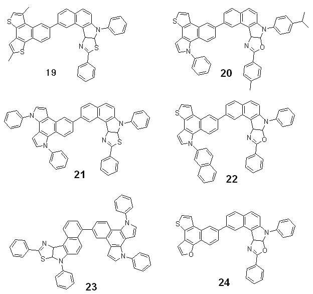
제 2 전극; 및
상기 제 1 전극 및 제 2 전극 사이에 개재된 유기층을 구비한 유기 발광 소자로서,
상기 유기층이 제 1 항 내지 제 6 항 중 어느 한 항의 화합물을 포함하는 유기 발광 소자.A first electrode;
A second electrode; And
An organic layer interposed between the first electrode and the second electrode,
Wherein the organic layer comprises the compound of any one of claims 1 to 6.
상기 유기층이 발광층인 유기 발광 소자. 8. The method of claim 7,
Wherein the organic layer is a light emitting layer.
상기 유기층이 녹색 인광 발광층인 유기 발광 소자.8. The method of claim 7,
Wherein the organic layer is a green phosphorescent light-emitting layer.
상기 유기층이 녹색 인광 발광층이며, 상기 화합물이 인광 호스트로 사용되는 유기 발광 소자.8. The method of claim 7,
Wherein the organic layer is a green phosphorescent light-emitting layer, and the compound is used as a phosphorescent host.
상기 유기 발광 소자가 전자 주입층, 전자 수송층, 발광층, 정공 주입층, 정공 수송층, 또는 정공 주입 및 정공 수송기능을 동시에 갖는 기능층을 포함하고,
상기 발광층은 제 1 항의 화합물 및 안트라센계 화합물을 포함하는 유기 발광 소자.8. The method of claim 7,
Wherein the organic light emitting device includes a functional layer having an electron injecting layer, an electron transporting layer, a light emitting layer, a hole injecting layer, a hole transporting layer, or a hole injecting and transporting function simultaneously,
Wherein the light emitting layer comprises the compound of claim 1 and an anthracene compound.
상기 유기 발광 소자가 전자 주입층 , 전자 수송층, 발광층, 정공 주입층, 정공 수송층, 또는 정공 주입 및 정공 수송기능을 동시에 갖는 기능층을 포함하고,
상기 발광층은 제 1 항의 화합물 및 아릴아민계 화합물을 포함하는 유기 발광 소자.8. The method of claim 7,
Wherein the organic light emitting device includes a functional layer having an electron injecting layer, an electron transporting layer, a light emitting layer, a hole injecting layer, a hole transporting layer, or a hole injecting and transporting function simultaneously,
Wherein the light emitting layer comprises the compound of claim 1 and an arylamine compound.
상기 유기 발광 소자가 전자 주입층, 전자 수송층, 발광층, 정공 주입층, 정공 수송층, 또는 정공 주입 및 정공 수송기능을 동시에 갖는 기능층을 포함하고,
상기 발광층은 제 1 항의 화합물 및 스티릴계 화합물을 포함하는 유기 발광 소자.8. The method of claim 7,
Wherein the organic light emitting device includes a functional layer having an electron injecting layer, an electron transporting layer, a light emitting layer, a hole injecting layer, a hole transporting layer, or a hole injecting and transporting function simultaneously,
Wherein the light emitting layer comprises the compound of claim 1 and a styryl compound.
상기 유기 발광 소자가 전자 주입층, 전자 수송층, 발광층, 정공 주입층, 정공 수송층, 또는 정공 주입 및 정공 수송기능을 동시에 갖는 기능층을 포함하고,
상기 발광층의 적색층, 녹색층, 청색층 또는 흰색층의 어느 한 층은 인광 화합물을 포함하는 유기 발광 소자.8. The method of claim 7,
Wherein the organic light emitting device includes a functional layer having an electron injecting layer, an electron transporting layer, a light emitting layer, a hole injecting layer, a hole transporting layer, or a hole injecting and transporting function simultaneously,
Wherein at least one of the red layer, green layer, blue layer or white layer of the light emitting layer comprises a phosphorescent compound.
상기 정공 주입층, 정공 수송층, 또는 정공 주입 기능 및 정공 수송 기능을 동시에 갖는 기능층이 전하 생성 물질을 포함하는 유기 발광 소자.15. The method of claim 14,
Wherein the hole injecting layer, the hole transporting layer, or the functional layer having both the hole injecting function and the hole transporting function comprise a charge generating material.
상기 전하 생성 물질이 p-도펀트이고, 상기 p-도펀트가 퀴논 유도체, 금속 산화물, 또는 시아노기-함유 화합물인 유기 발광 소자.16. The method of claim 15,
Wherein the charge generating material is a p-dopant, and the p-dopant is a quinone derivative, a metal oxide, or a cyano group-containing compound.
상기 유기층이 전자 수송층을 포함하고, 상기 전자 수송층이 전자 수송성 유기 화합물 및 금속 착체를 포함하는 유기 발광 소자.8. The method of claim 7,
Wherein the organic layer comprises an electron transporting layer, and the electron transporting layer comprises an electron transporting organic compound and a metal complex.
상기 금속 착제가 Li 착제인 유기 발광 소자.18. The method of claim 17,
Wherein the metal complex is a Li complex.
상기 유기층이 제 1 항 내지 제 6 항 중 어느 한 항의 화합물을 사용하여 습식 공정으로 형성되는 유기 발광 소자.8. The method of claim 7,
Wherein the organic layer is formed by a wet process using the compound of any one of claims 1 to 6.
Priority Applications (2)
| Application Number | Priority Date | Filing Date | Title |
|---|---|---|---|
| KR1020130023567A KR102162793B1 (en) | 2013-03-05 | 2013-03-05 | Compound and organic light emitting device comprising the same |
| US13/959,121 US9362507B2 (en) | 2013-03-05 | 2013-08-05 | Compound and organic light-emitting diode including the same |
Applications Claiming Priority (1)
| Application Number | Priority Date | Filing Date | Title |
|---|---|---|---|
| KR1020130023567A KR102162793B1 (en) | 2013-03-05 | 2013-03-05 | Compound and organic light emitting device comprising the same |
Publications (2)
| Publication Number | Publication Date |
|---|---|
| KR20140109177A true KR20140109177A (en) | 2014-09-15 |
| KR102162793B1 KR102162793B1 (en) | 2020-10-08 |
Family
ID=51486726
Family Applications (1)
| Application Number | Title | Priority Date | Filing Date |
|---|---|---|---|
| KR1020130023567A KR102162793B1 (en) | 2013-03-05 | 2013-03-05 | Compound and organic light emitting device comprising the same |
Country Status (2)
| Country | Link |
|---|---|
| US (1) | US9362507B2 (en) |
| KR (1) | KR102162793B1 (en) |
Families Citing this family (3)
| Publication number | Priority date | Publication date | Assignee | Title |
|---|---|---|---|---|
| KR102177211B1 (en) * | 2013-12-05 | 2020-11-11 | 삼성디스플레이 주식회사 | Organic light emitting device |
| US20200013959A1 (en) * | 2016-06-03 | 2020-01-09 | Lg Chem, Ltd. | Electroactive compounds |
| KR102490893B1 (en) * | 2017-09-29 | 2023-01-25 | 삼성디스플레이 주식회사 | Organic light emitting device and apparatus comprising the same |
Citations (4)
| Publication number | Priority date | Publication date | Assignee | Title |
|---|---|---|---|---|
| KR20120042478A (en) * | 2010-10-25 | 2012-05-03 | 삼성모바일디스플레이주식회사 | Heterocyclic compound and organic light emitting device containing same |
| KR20120127550A (en) * | 2011-05-11 | 2012-11-22 | 삼성디스플레이 주식회사 | Condensed-cyclic compound, organic light-emitting diode comprising the same, and flat display device |
| KR20130000229A (en) * | 2011-06-22 | 2013-01-02 | 삼성디스플레이 주식회사 | Heterocyclic compound and organic light emitting device containing same |
| KR20130000230A (en) * | 2011-06-22 | 2013-01-02 | 삼성디스플레이 주식회사 | Novel compound and organic light emitting device containing same |
Family Cites Families (4)
| Publication number | Priority date | Publication date | Assignee | Title |
|---|---|---|---|---|
| TWI541234B (en) | 2009-05-12 | 2016-07-11 | 環球展覽公司 | 2-azatriphenylene materials for organic light emitting diodes |
| KR20110113297A (en) | 2010-04-09 | 2011-10-17 | 다우어드밴스드디스플레이머티리얼 유한회사 | Novel compounds for organic electronic material and organic electroluminescent device using the same |
| US9056856B2 (en) | 2011-02-01 | 2015-06-16 | Semiconductor Energy Laboratory Co., Ltd. | Heterocyclic compound |
| KR101601679B1 (en) | 2011-08-08 | 2016-03-10 | 덕산네오룩스 주식회사 | Compound Containing 5-Membered Heterocycle And Organic Electronic Element Using The Same, Terminal Thereof |
-
2013
- 2013-03-05 KR KR1020130023567A patent/KR102162793B1/en active IP Right Grant
- 2013-08-05 US US13/959,121 patent/US9362507B2/en active Active
Patent Citations (4)
| Publication number | Priority date | Publication date | Assignee | Title |
|---|---|---|---|---|
| KR20120042478A (en) * | 2010-10-25 | 2012-05-03 | 삼성모바일디스플레이주식회사 | Heterocyclic compound and organic light emitting device containing same |
| KR20120127550A (en) * | 2011-05-11 | 2012-11-22 | 삼성디스플레이 주식회사 | Condensed-cyclic compound, organic light-emitting diode comprising the same, and flat display device |
| KR20130000229A (en) * | 2011-06-22 | 2013-01-02 | 삼성디스플레이 주식회사 | Heterocyclic compound and organic light emitting device containing same |
| KR20130000230A (en) * | 2011-06-22 | 2013-01-02 | 삼성디스플레이 주식회사 | Novel compound and organic light emitting device containing same |
Also Published As
| Publication number | Publication date |
|---|---|
| US9362507B2 (en) | 2016-06-07 |
| KR102162793B1 (en) | 2020-10-08 |
| US20140252324A1 (en) | 2014-09-11 |
Similar Documents
| Publication | Publication Date | Title |
|---|---|---|
| KR102188028B1 (en) | Organic light emitting device | |
| KR102117611B1 (en) | Organic light emitting device | |
| KR102117610B1 (en) | Heterocyclic compound and organic light emitting device comprising same | |
| KR20150014778A (en) | Oganic light emitting device | |
| KR102025834B1 (en) | Novel organic emitting compound, and organic light emitting diode comprising the same | |
| KR101994837B1 (en) | Novel heterocycle compound and organic light emitting device comprising the same | |
| KR102167041B1 (en) | Heterocyclic compound and organic light emitting device comprising same | |
| KR20140055137A (en) | Heterocyclic compound and organic light emitting device comprising the same | |
| KR102052071B1 (en) | Organic light emitting device | |
| KR20150104259A (en) | Organic light emitting device | |
| KR20150025259A (en) | Compound and organic light emitting device comprising the same | |
| KR20150007605A (en) | Iridium complex and Organic light emitting device comprising the same | |
| KR102154705B1 (en) | Heterocyclic compound and organic light emitting device comprising same | |
| KR20140144999A (en) | Iridium complex and Organic light emitting device comprising the same | |
| KR20130000229A (en) | Heterocyclic compound and organic light emitting device containing same | |
| KR102278600B1 (en) | Compound and organic light emitting device comprising same | |
| KR102167048B1 (en) | Compound and organic light emitting device comprising same | |
| KR101706742B1 (en) | Compound and organic light emitting device comprising same | |
| KR102087950B1 (en) | Heterocyclic compound and organic light emitting device comprising the same | |
| KR102173042B1 (en) | Heterocycle compound and organic light emitting device comprising same | |
| KR102253439B1 (en) | Heterocyclic compound and organic light emitting device comprising same | |
| KR20140018047A (en) | Novel condensation compound and organic light emitting device comprising the same | |
| KR102006879B1 (en) | Compound and organic light emitting device comprising the same | |
| KR102162793B1 (en) | Compound and organic light emitting device comprising the same | |
| KR102177211B1 (en) | Organic light emitting device |
Legal Events
| Date | Code | Title | Description |
|---|---|---|---|
| A201 | Request for examination | ||
| E902 | Notification of reason for refusal | ||
| E701 | Decision to grant or registration of patent right | ||
| GRNT | Written decision to grant |