KR20140096462A - Touch display device - Google Patents

Touch display device Download PDF

Info

Publication number
KR20140096462A
KR20140096462A KR1020130008918A KR20130008918A KR20140096462A KR 20140096462 A KR20140096462 A KR 20140096462A KR 1020130008918 A KR1020130008918 A KR 1020130008918A KR 20130008918 A KR20130008918 A KR 20130008918A KR 20140096462 A KR20140096462 A KR 20140096462A
Authority
KR
South Korea
Prior art keywords
terminal
signal
excitation coil
circuit
electrodes
Prior art date
Application number
KR1020130008918A
Other languages
Korean (ko)
Inventor
천대웅
Original Assignee
엘지디스플레이 주식회사
Priority date (The priority date is an assumption and is not a legal conclusion. Google has not performed a legal analysis and makes no representation as to the accuracy of the date listed.)
Filing date
Publication date
Application filed by 엘지디스플레이 주식회사 filed Critical 엘지디스플레이 주식회사
Priority to KR1020130008918A priority Critical patent/KR20140096462A/en
Publication of KR20140096462A publication Critical patent/KR20140096462A/en

Links

Images

Classifications

    • GPHYSICS
    • G06COMPUTING; CALCULATING OR COUNTING
    • G06FELECTRIC DIGITAL DATA PROCESSING
    • G06F3/00Input arrangements for transferring data to be processed into a form capable of being handled by the computer; Output arrangements for transferring data from processing unit to output unit, e.g. interface arrangements
    • G06F3/01Input arrangements or combined input and output arrangements for interaction between user and computer
    • G06F3/03Arrangements for converting the position or the displacement of a member into a coded form
    • G06F3/041Digitisers, e.g. for touch screens or touch pads, characterised by the transducing means
    • G06F3/046Digitisers, e.g. for touch screens or touch pads, characterised by the transducing means by electromagnetic means

Abstract

A touch display apparatus according to an embodiment of the present invention includes a display panel, and a display unit that is disposed on the display panel and includes an indicator for transmitting a position signal, a sensor unit for receiving a position signal transmitted from the indicator, And a position detection circuit for detecting a position on the basis of the position signal, wherein the sensor unit of the touch panel includes a Tx electrode and an Rx electrode arranged on the substrate and arranged to cross each other, And an exciting coil disposed on the substrate and surrounding the electrode portion, wherein the exciting coil is grounded or emits an electromagnetic field according to a signal of the position detecting circuit.

Description

{TOUCH DISPLAY DEVICE}

BACKGROUND OF THE INVENTION 1. Field of the Invention [0002] The present invention relates to a touch display device, and more particularly, to a touch display device capable of reducing a volume and manufacturing cost.

As the information and communication technology develops, computer peripherals such as keyboards, mice, joysticks, tablets and the like, which are the most basic input devices, are being developed, and the applications therefor are also developing. A tablet is a device that draws a corresponding image of a cursor on a computer screen when a tablet or a stylus, which is wirelessly connected to a flat, small flat plate, draws a picture on the tablet. The tablet is a kind of pointing device like a mouse, a graphic tablet, a digitizer tablet, It is also called electronic tablet.

Recently, the practical use of a display device has progressed, and a demand for a touch display device in which the above-described tablet is combined with a display device and can be directly input to a display device with a pen is increasing.

FIG. 1 is a view showing a conventional touch display device of a first type, and FIG. 2 is a view showing a conventional touch display device of a second type.

Referring to FIG. 1, in a conventional first touch display device, a Tx electrode 11 is formed on one surface of a base film 10 and an Rx electrode 12 is formed on the other surface. And a capacitive touch panel (TSP) to which a cover glass 15 and a protective film 14 are attached using an adhesive 13, respectively. A liquid crystal panel LCM, which is a display panel, is positioned below the touch panel TSP. The touch display device of the first type has an EM plate disposed under the liquid crystal panel (LCM) to supply energy to the pen and receive electromagnetic waves from the pen.

Referring to FIG. 2, the conventional touch display device of the second system includes the above-described touch panel TSP, and the Tx electrode 11 and the Rx electrode 12 serve to sense capacitive touch And receives electromagnetic waves from the pen. Then, an excitation coil is formed on the outside to supply energy to the pen.

The touch display device of the first and second schemes according to the related art has a problem that the volume and cost of the display device are increased because the EM display device is provided with an EM plate or an excitation coil to supply energy to the pen.

The present invention provides a touch display device capable of reducing the volume and manufacturing cost by forming an exciting coil in a touch panel.

According to an aspect of the present invention, there is provided a touch display apparatus including a display panel, a display panel disposed on the display panel and configured to transmit a position signal, a sensor configured to receive a position signal transmitted from the indicating body, And a position detection circuit for detecting a position on the basis of the position signal received by the sensor unit, wherein the sensor unit of the touch panel comprises: a Tx Wherein the excitation coil is grounded or emits an electromagnetic field according to a signal of the position detection circuit. The excitation coil includes a first electrode, a second electrode, and an Rx electrode. The excitation coil surrounds the electrode, do.

The position detection circuit includes a drive circuit for applying a current to the excitation coil and an oscillator for outputting an AC signal of a predetermined frequency to the drive circuit.

The drive circuit includes a switch including a first terminal connected to the exciting coil, a second terminal connected to the ground, and a third terminal connected to the oscillator.

And the switch connects the first terminal to the second terminal or connects the first terminal to the third terminal under the control of the control unit.

And when the first terminal is connected to the second terminal by the switch, the excitation coil is grounded.

And when the first terminal is connected to the third terminal by the switch, the excitation coil emits an electromagnetic field.

And the AC signal applied from the oscillator is converted into a current in the drive circuit and supplied to the excitation coil.

And the exciting coil is wound around the electrode portion by N (natural number).

A touch display device according to an embodiment of the present invention includes excitation coils in a touch panel and performs both a function of grounding and a dissipation of an electromagnetic field to thereby shield the touch noise in the touch panel and reduce the volume and manufacturing cost of the touch display device There is an advantage to be able to do.

BRIEF DESCRIPTION OF THE DRAWINGS Fig.
Fig. 2 is a view showing a touch display device of the entry type. Fig.
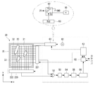
3 is a schematic view of a touch display device according to an embodiment of the present invention.
Figure 4 is a schematic representation of an indicator in accordance with an embodiment of the present invention.
5 is a circuit diagram showing an integrated circuit of indicator.
6 is a plan view of a touch panel according to an embodiment of the present invention.
FIG. 7 is an enlarged view of the area A in FIG. 6; FIG.
Fig. 8A is a diagram illustrating the ground of the exciting coil, and Fig. 8B is a diagram schematically illustrating that current is supplied to the exciting coil.
9 is a waveform diagram showing a waveform supplied to the exciting coil;
10 is a view showing a manufacturing method for forming an excitation coil according to the present invention by a process.
11 to 14 are views showing various structures of the touch display device.
Fig. 15 is a diagram showing the electromagnetic field of a touch display device having a wound coil wound once. Fig.
16 is a view showing an electromagnetic field measurement of a touch display device having an exciting coil wound five times.

Hereinafter, embodiments of the present invention will be described in detail with reference to the accompanying drawings.

FIG. 3 is a schematic view of a touch display device according to an embodiment of the present invention, and FIG. 4 is a diagram illustrating a pointing device according to an embodiment of the present invention.

3, the touch panel 1 includes a sensor unit 30 for detecting the position of the indicating unit 20, a selecting circuit 40 for selecting a plurality of electrodes constituting the sensor unit 30, And a position detection circuit (50).

The sensor unit 30 includes a plurality of Tx electrodes 31 extending in the x axis direction and a plurality of Rx electrodes 33 extending in the y axis direction intersecting the extending direction of the Tx electrode 31. [ (Not shown). And an excitation coil 35 disposed so as to surround the electrode portion 32. The Tx electrodes 31 and the Rx electrodes 33 are respectively connected to the selection circuit 40 and the excitation coil 35 is connected to the drive circuit 61 described later in the position detection circuit 50.

The number and pitch of the Tx electrodes 31 and the Rx electrodes 33 are appropriately set in accordance with the size of the sensor unit 30 and the required detection accuracy. In the present embodiment, the Tx electrodes 31 and the Rx electrodes 33 are exemplified as linear conductors, but the present invention is not limited to this, and may extend in a ring shape.

The selection circuit 40 selects the Tx electrodes 31 and the Rx electrodes 33 in a predetermined order. The selection control of the electrodes by the selection circuit 40 is controlled by a control signal output by the control unit 63, which will be described later, in cooperation with the central processing unit 62. [ The selection circuit 220 includes a first selection circuit 221 and a second selection circuit 222. The first selection circuit 221 is connected to the plurality of Tx electrodes 31 and the second selection circuit 222 is connected to the plurality of Rx electrodes 33. [ The switching control of the first selection circuit 221 and the second selection circuit 222 is controlled by a control signal output from the control unit 63 cooperating with the central processing unit 62. By repeating the sequential selection of the Tx electrodes 31 and the Rx electrodes 33, it becomes possible to substantially simultaneously detect different kinds of indicating bodies, such as a pen or a finger, placed on the sensor unit 30.

The position detection circuit 50 includes a receiving system circuit group 51, an oscillator 60, a drive circuit 61, a central processing unit 62 (Central Processing Unit), and a control unit 63.

The receiving circuit group 51 includes a receiving amplifier 52 and an A / D (analog to digital) converting circuit 53, a detecting unit 54, a memory unit 55 and a detecting unit 56. The receiving amplifier 52, the A / D converting circuit 53, the detecting section 54, the memory section 55 and the detecting section 56 are sequentially connected from the selecting circuit 40 side.

The reception amplifier 52 amplifies the reception signal supplied from the constant electrodes selected by the selection circuit 40. Then, the reception amplifier 52 outputs the amplified reception signal to the A / D conversion circuit 53. The A / D conversion circuit 53 analog-to-digital converts the amplified reception signal and outputs the converted digital signal to the detection section 54.

The detection section 54 performs synchronous detection on the received signal to detect the signal of the first frequency f1 and the signal of the second frequency f2. The detection unit 54 outputs the signal of the first frequency f1 and the signal of the second frequency f2 detected for each electrode to the memory unit 55. [

The detection unit 56 calculates the position (coordinate) of the indicating unit 20 by using the information of each frequency stored in the memory unit 55. [ More specifically, the detection unit 56 detects the level of the received signal of the first frequency f1, compares the level of the received signal with the predetermined threshold value, and determines that the first frequency f1 is transmitted from the indicating body 20 And the position of the indicating body 20 is detected. Similarly, the level of the received signal at the second frequency f2 is detected, and the level is compared with a predetermined threshold value to recognize that the second frequency f2 is transmitted from the indicating body 20. [ The same frequency recognition processing is performed for the case where other frequencies exist.

The oscillator 60 outputs an AC signal of a predetermined frequency to the drive circuit 61. The drive circuit 61 converts the AC signal inputted from the oscillator 60 into a current and supplies it to the exciting coil 35. [ The drive circuit 61 includes a switch T3 including a first terminal T1 connected to the excitation coil 35, a second terminal T2 connected to the ground GND and a third terminal T3 connected to the oscillator 60, (62). The switch 62 connects the first terminal T1 to the second terminal T2 or connects the first terminal T1 to the third terminal T3 under the control of the control unit.

The switch 62 is operated under the control of the control unit 63. When the first terminal T1 is connected to the second terminal T2 by the switch 62, the excitation coil 35 is grounded, So that the exciting coil 35 acts as a ground wiring to remove the static electricity of the substrate. When the first terminal T1 is connected to the third terminal T3 by the switch 62, the exciting coil 35 radiates an electromagnetic field to transmit an excitation signal to the indicating body 20. [ do.

On the other hand, the control unit 63 cooperating with the central processing unit 62 outputs control signals to the respective units in the position detection circuit 50 and outputs the calculation results of the detection unit 56 in the reception system circuit group 51 as And outputs it to the external device through the central processing unit 62. [ The operation of the control unit 63 is controlled by the central processing unit 62. [

Fig. 4 is a diagram showing an indicator according to an embodiment of the present invention, and Fig. 5 is a circuit diagram showing an indicator integrated circuit. In the following, an indicator indicating the position and the pressure of the indicator is described as an example, but the present invention is not limited thereto.

Referring to FIG. 4, the indicator 20 includes a coil 21a wound around a ferrite core 37 and a variable capacity capacitor 22 whose capacity is changed by a pressure. One end of the core 38 engages with a pen tip 23. And is connected to the variable capacitance condenser 22 through the ferrite core 37. The printed circuit board 24 is also mounted with an integrated circuit and its peripheral components. According to this configuration, the variable capacity condenser 22 is pressed by the core 38 and its capacity is changed in response to the application of the pressure to the pen tip 23.

5, the coil 21a and the condenser 21b constitute a resonance circuit 21 that resonates at a frequency output from the excitation coil 35 as a position detection device. The integrated circuit 25 is driven by the driving power generated by the diode 26 and the condenser 27. The diode 26 is connected to the resonance circuit 21 and an AC voltage generated in the resonance circuit 21 based on an excitation signal supplied from the excitation coil 35 is rectified by the diode 26, (27) and becomes a driving power source. The signal generated in the resonance circuit 21 is supplied to the integrated circuit 25 through the condenser 28. [ In the integrated circuit 25, a clock signal used for transmitting and receiving signals between the position indicator 2 and the sensor unit and a clock signal for detecting the pressure are generated based on a signal supplied through the capacitor 28 .

In addition, the capacity of the variable capacity capacitor 22 is changed by the pressure. The variable capacitance capacitor 22 is connected to a resistor to constitute a time constant circuit, and the time constant is changed in accordance with the capacitance which varies with the pressure. Corresponding to the time corresponding to this time constant, the number of waves of the signal generated in the resonance circuit 21 is measured by the integrated circuit 25. The measured value is converted into a predetermined number of bits, for example, a value of 8 bits. The pressure data obtained in this manner is output from the IC 25 one bit at a time in synchronization with the clock signal provided for transmission and reception of signals between the indicator 20 and the switch 20 connected in parallel to the resonance circuit 21. [ (29). Therefore, when the switch 29 is off, the signal from the indicating unit 20 can be detected. When the switch 29 is on, the resonance circuit 21 is shunted so that the signal sent out from the indicating unit 20 can be detected none. Thus, in the touch display device 1, the pressure can be obtained by detecting a signal transmitted from the indicating device 20 after transmitting the exciting signal from the exciting coil 35 for a predetermined time.

6 is an enlarged view of an area A of FIG. 6, FIG. 8A is a diagram illustrating a ground of an excitation coil, FIG. 8B is a view showing a touch panel according to an embodiment of the present invention, Fig. 9 is a waveform diagram showing a waveform supplied to the exciting coil; Fig.

6 and 7, a plurality of Tx electrodes 31 arranged in the transverse direction and a plurality of Rx electrodes 33 arranged in the longitudinal direction are formed on the substrate 70, Is formed. The Tx electrodes 31 and the Rx electrodes 33 are connected to the Tx electrode pad 36 and the Rx electrode pad 39 disposed on one side of the substrate 70 through the routing wirings 34, respectively.

The excitation coil 35 is formed on the substrate 70 on which the sensing unit 32 is formed and surrounds the sensing unit 32. The exciting coil 35 is formed in a shape wound around the sensing portion 32. Both ends of the exciting coil 35 are connected to the exciting coil pads 40 and connected to the driver circuit 61 described in Fig.

Referring to FIG. 8A, the exciting coil 35 formed on the substrate (not shown) is grounded by a switch 62 provided in the driver circuit described in FIG. When the exciting coil 35 is grounded, external noise is guided to the ground line to shield the noise at the time of touch and to block the interference signal between the Tx electrodes and the Rx electrodes.

8B, when an electric current is supplied to the exciting coil 35 by the switch 62, the exciting coil 35 emits an electromagnetic field. The electromagnetic field radiated from the exciting coil 35 supplies energy to the resonating circuit inside the indicating body 20, such as a styro pen. When the energy stored in the pointing device 20 is radiated at the moment when the energy supply is interrupted, the sensor unit senses the energy and the position can be determined.

Referring to FIG. 9, a signal supplied to the exciting coil 35 is time-divided and applied to the electromagnetic field section I and the ground section II. The signal supplied to the exciting coil 35 is controlled by a driver circuit. More specifically, the electromagnetic field interval I is defined as a signal recognition interval, and the ground interval II is defined as a signal non-recognition interval. Here, the signal unrecognized period corresponds to the ground level, and the signal recognition period swings between positive and negative based on the ground level. In FIG. 9 of the present invention, the waveform of the signal applied to the electromagnetic section I is applied at a constant width and a constant period. However, the present invention is not limited to this and may be applied at an irregular width and period.

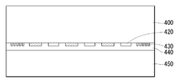
The above-mentioned excitation coil can be formed on the substrate of the touch panel. FIG. 10 is a view showing a manufacturing method for forming an excitation coil according to the present invention, and FIG. 11 to FIG. 14 are views showing various structures of a touch display device.

Referring to FIG. 10A, a metal layer 120 is formed by depositing a metal material on a substrate 110. The substrate 110 may be a glass substrate or a film substrate such as PET or the like and may be copper (Cu) or APC (Ag / Pd / Cu alloy). 10 (b), a photoresist layer 130 is formed by applying a photoresist on the metal layer 120. Next, as shown in FIG.

10 (c), the photoresist layer 130 is exposed and developed to form a photoresist pattern 135 on the region of the metal layer 120 where the excitation coil is to be formed. Referring to FIG. 10D, the metal layer 120 is etched using the photoresist pattern 135 as a mask to form the exciting coil 125. At this time, the metal layer 120 masked by the photoresist pattern 135 remains and is formed of the exciting coil 125, and the metal layer 120 in the region where the photoresist pattern 135 is not formed is completely removed.

10E, a photoresist pattern 135 is stripped to finally form an exciting coil 125 on the substrate 110. [0052] Next, as shown in FIG. The excitation coil 125 is formed to be rotated by a number of N (natural number) so that a large amount of electromagnetic waves can be radiated.

The excitation coil 125 thus formed can be applied to various touch display devices.

11, Tx electrodes 310 are formed on one surface of a cover substrate 300 and Rx electrodes 330 are formed on an insulating layer 320 insulating the Tx electrodes 310 do. The manufactured cover substrate 330 is bonded to the liquid crystal panel 360, which is a display panel, through the optical adhesive 350. In such a touch display apparatus, the exciting coil 340 is formed on one surface of the cover substrate 300 on which the Tx electrodes 310 are formed. At this time, the exciting coil 340 is formed so as to contact or not overlap the Tx electrode 310 and the Rx electrode 330.

12, Tx electrodes 410 are formed on the upper surface of the cover substrate 400, and Rx electrodes 420 are formed on the lower surface of the cover substrate 400. FIG. The cover substrate 400 thus formed is bonded to the liquid crystal panel 450 using an optical adhesive 440. At this time, the exciting coil 430 is formed on the lower surface of the cover substrate 400 on which the Rx electrodes 420 are formed. However, the excitation coil 430 of the present invention may be formed on the upper surface of the cover substrate 400 on which the Tx electrodes 410 are formed.

13, the Tx electrodes 520 are formed on the upper surface of the support film 510, and the Rx electrodes 530 are formed on the lower surface of the support film 510. The cover substrate 500 is bonded to the upper surface of the support film 510 through the optical adhesive 550 and the liquid crystal panel 560 is bonded to the lower surface of the support film 510 through the optical adhesive 550. In such a touch display apparatus, the exciting coil 540 is formed on the lower surface of the supporting film 510 on which the Rx electrodes 540 are formed. However, the excitation coil 540 of the present invention is not limited thereto, and may be formed on the upper surface of the support film 510 on which the Tx electrodes 520 are formed.

14, the Tx electrodes 620 are formed on the first support film 610 and the Rx electrodes 640 are formed on the second support film 630. In addition, The cover substrate 600 is adhered to the upper surface of the first support film 610 using the optical adhesive 650 and the second support film 610 is attached to the lower surface of the first support film 610 using the optical adhesive 650. [ The film 630 is bonded. Further, the liquid crystal panel 660 is bonded to the lower surface of the second support film 630 using the optical adhesive 650. In such a touch display device, the exciting coil 670 is formed on the second supporting film 630 on which the Rx electrodes 640 are formed. However, the exciting coil 670 of the present invention may be formed on the first supporting film 610 on which the Tx electrodes 620 are formed.

FIG. 15 is a view showing an electromagnetic field measurement of a touch display device having a single-turn excitation coil, and FIG. 16 is a view showing an electromagnetic field measurement of a touch display device having an excitation coil wound five times.

15 and 16, it can be seen that the intensity of the electromagnetic field of the exciting coil wound five times is superior to the intensity of the electromagnetic field of the once wound exciting coil. Therefore, the exciting coil of the present invention can efficiently adjust the intensity of the electromagnetic field by winding the electrode part N (natural number).

As described above, the touch display device according to an embodiment of the present invention includes excitation coils in the touch panel, and functions as both the ground and the electromagnetic field divergence, thereby shielding the touch noise in the touch panel, There is an advantage that the manufacturing cost can be reduced.

While the present invention has been described in connection with what is presently considered to be practical exemplary embodiments thereof, it is to be understood that the invention is not limited to the disclosed embodiments, but, on the contrary, It will be understood that the invention may be practiced. It is therefore to be understood that the embodiments described above are to be considered in all respects only as illustrative and not restrictive. In addition, the scope of the present invention is indicated by the following claims rather than the detailed description. Also, all changes or modifications derived from the meaning and scope of the claims and their equivalents should be construed as being included within the scope of the present invention.

70: substrate 31: Tx electrode
32: sensing part 33: Rx electrode
34: routing wiring 35: exciting coil
36: Tx electrode pad 39: Rx electrode pad
40: Female coil pad

Claims (8)

Display panel; And
And a position detecting circuit for detecting a position based on the position signal received by the sensor unit, wherein the position detecting circuit comprises: And a touch panel including the touch panel,
The sensor unit of the touch panel includes:
And an excitation coil disposed on the substrate and surrounding the electrode portion, wherein the excitation coil is connected to the signal of the position detection circuit And the touch panel is grounded or emits an electromagnetic field according to the touch panel.
The method according to claim 1,
Wherein the position detection circuit includes a drive circuit for applying a current to the excitation coil and an oscillator for outputting an AC signal of a predetermined frequency to the drive circuit.
3. The method of claim 2,
Wherein the drive circuit includes a switch including a first terminal connected to the exciting coil, a second terminal connected to the ground, and a third terminal connected to the oscillator.
The method of claim 3,
Wherein the switch connects the first terminal to the second terminal or connects the first terminal to the third terminal under the control of the control unit.
5. The method of claim 4,
Wherein when the first terminal is connected to the second terminal by the switch, the excitation coil is grounded.
5. The method of claim 4,
Wherein when the first terminal is connected to the third terminal by the switch, the excitation coil emits an electromagnetic field.
The method according to claim 6,
Wherein the AC signal applied from the oscillator is converted into a current in the drive circuit and supplied to the excitation coil.
The method according to claim 1,
And the excitation coil is wound around the electrode portion by N (natural number).
KR1020130008918A 2013-01-25 2013-01-25 Touch display device KR20140096462A (en)

Priority Applications (1)

Application Number Priority Date Filing Date Title
KR1020130008918A KR20140096462A (en) 2013-01-25 2013-01-25 Touch display device

Applications Claiming Priority (1)

Application Number Priority Date Filing Date Title
KR1020130008918A KR20140096462A (en) 2013-01-25 2013-01-25 Touch display device

Publications (1)

Publication Number Publication Date
KR20140096462A true KR20140096462A (en) 2014-08-06

Family

ID=51744299

Family Applications (1)

Application Number Title Priority Date Filing Date
KR1020130008918A KR20140096462A (en) 2013-01-25 2013-01-25 Touch display device

Country Status (1)

Country Link
KR (1) KR20140096462A (en)

Similar Documents

Publication Publication Date Title
JP6153042B2 (en) Touch sensing system and display device
US8564553B2 (en) Electronic stylus, capacitive touchpad module, and apparatus for touch input
US7292229B2 (en) Transparent digitiser
TWI510999B (en) Touch input system and method for detecting touch using the same
CN107111409B (en) Touch pen, touch panel and coordinate indicating system with same
EP2034395B1 (en) Position detecting device and position detecting method
JP2011065450A (en) Position detector and pointer
TWI554935B (en) Electromagnetic induction input device
CN106843539B (en) Wireless passive handwriting input system
KR20140096462A (en) Touch display device
CN110456926B (en) Electromagnetic pen, electromagnetic input system and electromagnetic input method
KR102216328B1 (en) Touch screen device
KR20190108747A (en) Touch Sensor Integrated Digitizer
US20230280860A1 (en) Input device with near-field communication
EP4209869A1 (en) Electronic device and control method therefor, touch system, and chip system
KR101811408B1 (en) Touch input device, touch detector and touch detecting method using electromagnetic induction position detection sensor
KR20160128042A (en) Electromagnetic pen
JP6069469B2 (en) Position indicator and position detection device
TWM444557U (en) Wireless pen

Legal Events

Date Code Title Description
A201 Request for examination
E902 Notification of reason for refusal
E601 Decision to refuse application