KR20140085657A - Semiconductor device with air gap and method for fabricating the same - Google Patents
Semiconductor device with air gap and method for fabricating the same Download PDFInfo
- Publication number
- KR20140085657A KR20140085657A KR1020120153830A KR20120153830A KR20140085657A KR 20140085657 A KR20140085657 A KR 20140085657A KR 1020120153830 A KR1020120153830 A KR 1020120153830A KR 20120153830 A KR20120153830 A KR 20120153830A KR 20140085657 A KR20140085657 A KR 20140085657A
- Authority
- KR
- South Korea
- Prior art keywords
- layer
- forming
- plug
- storage node
- capping
- Prior art date
Links
Images


Classifications
-
- H—ELECTRICITY
- H01—ELECTRIC ELEMENTS
- H01L—SEMICONDUCTOR DEVICES NOT COVERED BY CLASS H10
- H01L21/00—Processes or apparatus adapted for the manufacture or treatment of semiconductor or solid state devices or of parts thereof
- H01L21/70—Manufacture or treatment of devices consisting of a plurality of solid state components formed in or on a common substrate or of parts thereof; Manufacture of integrated circuit devices or of parts thereof
- H01L21/71—Manufacture of specific parts of devices defined in group H01L21/70
- H01L21/768—Applying interconnections to be used for carrying current between separate components within a device comprising conductors and dielectrics
- H01L21/76801—Applying interconnections to be used for carrying current between separate components within a device comprising conductors and dielectrics characterised by the formation and the after-treatment of the dielectrics, e.g. smoothing
- H01L21/7682—Applying interconnections to be used for carrying current between separate components within a device comprising conductors and dielectrics characterised by the formation and the after-treatment of the dielectrics, e.g. smoothing the dielectric comprising air gaps
-
- H—ELECTRICITY
- H01—ELECTRIC ELEMENTS
- H01L—SEMICONDUCTOR DEVICES NOT COVERED BY CLASS H10
- H01L21/00—Processes or apparatus adapted for the manufacture or treatment of semiconductor or solid state devices or of parts thereof
- H01L21/70—Manufacture or treatment of devices consisting of a plurality of solid state components formed in or on a common substrate or of parts thereof; Manufacture of integrated circuit devices or of parts thereof
- H01L21/71—Manufacture of specific parts of devices defined in group H01L21/70
- H01L21/76—Making of isolation regions between components
- H01L21/764—Air gaps
-
- H—ELECTRICITY
- H01—ELECTRIC ELEMENTS
- H01L—SEMICONDUCTOR DEVICES NOT COVERED BY CLASS H10
- H01L21/00—Processes or apparatus adapted for the manufacture or treatment of semiconductor or solid state devices or of parts thereof
- H01L21/70—Manufacture or treatment of devices consisting of a plurality of solid state components formed in or on a common substrate or of parts thereof; Manufacture of integrated circuit devices or of parts thereof
- H01L21/71—Manufacture of specific parts of devices defined in group H01L21/70
- H01L21/768—Applying interconnections to be used for carrying current between separate components within a device comprising conductors and dielectrics
- H01L21/76801—Applying interconnections to be used for carrying current between separate components within a device comprising conductors and dielectrics characterised by the formation and the after-treatment of the dielectrics, e.g. smoothing
- H01L21/76829—Applying interconnections to be used for carrying current between separate components within a device comprising conductors and dielectrics characterised by the formation and the after-treatment of the dielectrics, e.g. smoothing characterised by the formation of thin functional dielectric layers, e.g. dielectric etch-stop, barrier, capping or liner layers
- H01L21/76831—Applying interconnections to be used for carrying current between separate components within a device comprising conductors and dielectrics characterised by the formation and the after-treatment of the dielectrics, e.g. smoothing characterised by the formation of thin functional dielectric layers, e.g. dielectric etch-stop, barrier, capping or liner layers in via holes or trenches, e.g. non-conductive sidewall liners
-
- H—ELECTRICITY
- H01—ELECTRIC ELEMENTS
- H01L—SEMICONDUCTOR DEVICES NOT COVERED BY CLASS H10
- H01L21/00—Processes or apparatus adapted for the manufacture or treatment of semiconductor or solid state devices or of parts thereof
- H01L21/70—Manufacture or treatment of devices consisting of a plurality of solid state components formed in or on a common substrate or of parts thereof; Manufacture of integrated circuit devices or of parts thereof
- H01L21/71—Manufacture of specific parts of devices defined in group H01L21/70
- H01L21/768—Applying interconnections to be used for carrying current between separate components within a device comprising conductors and dielectrics
- H01L21/76897—Formation of self-aligned vias or contact plugs, i.e. involving a lithographically uncritical step
-
- H—ELECTRICITY
- H10—SEMICONDUCTOR DEVICES; ELECTRIC SOLID-STATE DEVICES NOT OTHERWISE PROVIDED FOR
- H10B—ELECTRONIC MEMORY DEVICES
- H10B12/00—Dynamic random access memory [DRAM] devices
-
- H—ELECTRICITY
- H10—SEMICONDUCTOR DEVICES; ELECTRIC SOLID-STATE DEVICES NOT OTHERWISE PROVIDED FOR
- H10B—ELECTRONIC MEMORY DEVICES
- H10B99/00—Subject matter not provided for in other groups of this subclass
-
- H—ELECTRICITY
- H01—ELECTRIC ELEMENTS
- H01L—SEMICONDUCTOR DEVICES NOT COVERED BY CLASS H10
- H01L21/00—Processes or apparatus adapted for the manufacture or treatment of semiconductor or solid state devices or of parts thereof
- H01L21/70—Manufacture or treatment of devices consisting of a plurality of solid state components formed in or on a common substrate or of parts thereof; Manufacture of integrated circuit devices or of parts thereof
- H01L21/71—Manufacture of specific parts of devices defined in group H01L21/70
- H01L21/768—Applying interconnections to be used for carrying current between separate components within a device comprising conductors and dielectrics
- H01L21/76838—Applying interconnections to be used for carrying current between separate components within a device comprising conductors and dielectrics characterised by the formation and the after-treatment of the conductors
- H01L21/76841—Barrier, adhesion or liner layers
- H01L21/76843—Barrier, adhesion or liner layers formed in openings in a dielectric
- H01L21/76847—Barrier, adhesion or liner layers formed in openings in a dielectric the layer being positioned within the main fill metal
Abstract
Description
본 발명은 반도체장치에 관한 것으로서, 상세하게는 에어갭을 갖는 반도체장치 및 그 제조 방법에 관한 것이다.The present invention relates to a semiconductor device, and more particularly, to a semiconductor device having an air gap and a manufacturing method thereof.
일반적으로 반도체 장치는 복수의 제1도전구조물들 사이에 절연층을 사이에 두고 형성된 제2도전구조물을 포함한다. 예를 들어, 제1도전구조물은 게이트, 비트라인, 금속배선 등을 포함할 수 있고, 제2도전구조물은 콘택플러그, 스토리지노드콘택플러그, 비트라인콘택플러그, 비아 등을 포함할 수 있다.Generally, a semiconductor device includes a second conductive structure formed between a plurality of first conductive structures with an insulating layer interposed therebetween. For example, the first conductive structure may include a gate, a bit line, a metal line, and the like, and the second conductive structure may include a contact plug, a storage node contact plug, a bit line contact plug, a via, and the like.
반도체 장치가 고집적화됨에 따라, 제1도전구조물과 제2도전구조물이 서로 이격되는 거리가 점점 가까워지고 있다. 이로 인해, 제1도전구조물과 제2도전구조물 사이의 기생캐패시턴스가 증가되고 있다. 기생캐패시턴스가 증가됨에 따라 반도체장치의 동작 속도가 느려지고, 리프레시 특성이 열화된다.As the semiconductor device becomes highly integrated, the distance that the first conductive structure and the second conductive structure are separated from each other is gradually getting closer. This increases the parasitic capacitance between the first conductive structure and the second conductive structure. As the parasitic capacitance is increased, the operation speed of the semiconductor device is slowed and the refresh characteristic is deteriorated.
기생캐패시턴스를 감소시키기 위해 절연층의 유전율을 낮추는 방법이 있다. 반도체 장치에서 일반적으로 사용되는 절연층으로는 실리콘산화물과 실리콘질화물이 있다. 실리콘산화물은 유전율이 약 4이고, 실리콘질화물은 유전율이 약 7이다.There is a method of lowering the dielectric constant of the insulating layer to reduce the parasitic capacitance. Silicon oxide and silicon nitride are commonly used as insulating layers in semiconductor devices. Silicon oxide has a dielectric constant of about 4, and silicon nitride has a dielectric constant of about 7.
실리콘산화물과 실리콘질화물은 여전히 높은 유전율을 갖기 때문에 기생캐패시턴스를 감소시키는데 한계가 있다. 최근에 상대적으로 낮은 유전율의 물질을 개발하고 있으나 이들또한 유전율이 그리 낮지 않은 것이 현실이다.Silicon oxide and silicon nitride still have a high permittivity, which limits their ability to reduce parasitic capacitance. Recently, materials with relatively low permittivity have been developed, but they also have a low permittivity.
본 발명의 실시예들은 이웃한 도전구조물들간의 기생캐패시턴스를 감소시킬 수 있는 반도체장치 및 그 제조 방법을 제공한다.Embodiments of the present invention provide a semiconductor device capable of reducing parasitic capacitance between neighboring conductive structures and a method of manufacturing the same.
본 발명의 실시예에 따른 반도체장치 제조 방법은 기판 상에 오픈부를 갖는 반도체구조물을 형성하는 단계, 상기 오픈부의 측벽에 희생스페이서를 형성하는 단계, 상기 오픈부에 리세스된 제1플러그를 형성하는 단계, 상기 희생스페이서를 제거하여 에어갭을 형성하는 단계, 상기 제1플러그의 상부표면을 노출시키고 상기 에어갭을 캡핑하는 캡핑층을 형성하는 단계, 상기 캡핑층 및 제1플러그 상에 보호층을 형성하는 단계, 상기 보호층 상에 오믹콘택층을 형성하는 단계, 및 상기 오믹콘택층 상에 제2플러그를 형성하는 단계를 포함할 수 있다. 상기 캡핑층을 형성하는 단계는 상기 제1플러그의 표면을 산화시켜 산화물을 형성하는 단계; 및 상기 제1플러그의 상부 표면이 노출되도록 상기 산화물을 선택적으로 제거하는 단계를 포함할 수 있다. 상기 보호층을 형성하는 단계는 상기 캡핑층 및 제1플러그를 포함한 전면에 폴리실리콘층을 갭필하는 단계; 및 상기 폴리실리콘층을 에치백하는 단계를 포함할 수 있다. 상기 오믹콘택층을 형성하는 단계는 상기 보호층 상에 실리사이드화가능금속층을 형성하는 단계; 어닐을 실시하여 상기 보호층과 실리사이드화가능금속층을 반응시켜 금속실리사이드를 형성하는 단계; 및 미반응 상기 실리사이드화가능금속층을 스트립하는 단계를 포함할 수 있다.A semiconductor device manufacturing method according to an embodiment of the present invention includes the steps of forming a semiconductor structure having an open portion on a substrate, forming a sacrificial spacer on a sidewall of the open portion, forming a recessed first plug in the open portion Removing the sacrificial spacers to form an air gap; exposing an upper surface of the first plug and forming a capping layer to cap the air gap; forming a capping layer and a protective layer on the first plug Forming an ohmic contact layer on the protective layer, and forming a second plug on the ohmic contact layer. Wherein forming the capping layer comprises: oxidizing the surface of the first plug to form an oxide; And selectively removing the oxide so that the upper surface of the first plug is exposed. The forming of the passivation layer may include: capping a polysilicon layer over the entire surface including the capping layer and the first plug; And etching back the polysilicon layer. Wherein forming the ohmic contact layer comprises: forming a silicidizable metal layer on the protective layer; Performing an anneal to react the protective layer and the silicidizable metal layer to form a metal silicide; And stripping the unreacted portion of the silicidable metal layer.
본 발명의 실시예에 따른 반도체장치 제조 방법은 기판 상에 복수의 비트라인구조물을 형성하는 단계, 상기 비트라인구조물 사이에 스토리지노드콘택홀을 형성하는 단계, 상기 스토리지노드콘택홀의 측벽에 희생스페이서를 형성하는 단계, 상기 스토리지노드콘택홀에 리세스된 제1스토리지노드콘택플러그를 형성하는 단계, 상기 희생스페이서를 제거하여 에어갭을 형성하는 단계, 상기 제1스토리지노드콘택플러그의 표면을 산화시켜 산화물을 형성하는 단계, 상기 제1스토리지노드콘택플러그의 상부 표면을 노출시키도록 상기 산화물을 식각하여 상기 에어갭을 캡핑하는 캡핑층을 형성하는 단계, 상기 캡핑층 및 제1스토리지노드콘택플러그 상에 보호층을 형성하는 단계, 상기 보호층 상에 오믹콘택층을 형성하는 단계, 및 상기 오믹콘택층 상에 제2스토리지노드콘택플러그를 형성하는 단계를 포함할 수 있다.A method for fabricating a semiconductor device according to an embodiment of the present invention includes forming a plurality of bit line structures on a substrate, forming a storage node contact hole between the bit line structures, forming a sacrificial spacer on a sidewall of the storage node contact hole Forming a first storage node contact plug recessed in the storage node contact hole, removing the sacrificial spacers to form an air gap, oxidizing the surface of the first storage node contact plug to form oxide Forming a capping layer for capping the air gap by etching the oxide to expose an upper surface of the first storage node contact plug, forming a capping layer on the capping layer and the first storage node contact plug Forming an ohmic contact layer on the ohmic contact layer, forming an ohmic contact layer on the ohmic contact layer, Storage may comprise the step of forming a node contact plug.
본 발명의 실시예에 따른 반도체장치는 기판 상에 형성된 복수의 비트라인구조물, 상기 비트라인구조물의 측벽을 노출시키도록 형성된 스토리지노드콘택홀, 상기 스토리지노드콘택홀에 리세스되어 형성된 제1스토리지노드콘택플러그, 상기 비트라인구조물의 측벽과 상기 제1스토리지노드콘택플러그 사이에 형성된 에어갭, 상기 에어갭을 캡핑하는 캡핑층, 상기 캡핑층 및 제1스토리지노드콘택플러그 상에 형성된 보호층, 상기 보호층 상에 형성된 오믹콘택층, 및 상기 오믹콘택층 상에 형성된 제2스토리지노드콘택플러그를 포함할 수 있다.A semiconductor device according to an embodiment of the present invention includes a plurality of bit line structures formed on a substrate, a storage node contact hole formed to expose sidewalls of the bit line structure, a first storage node A contact plug, an air gap formed between the sidewall of the bit line structure and the first storage node contact plug, a capping layer capping the air gap, a protection layer formed on the capping layer and the first storage node contact plug, An ohmic contact layer formed on the layer, and a second storage node contact plug formed on the ohmic contact layer.
본 발명의 실시예에 따른 반도체장치는 기판 상에 형성되고 오픈부를 갖는 반도체구조물, 상기 오픈부에 리세스되어 형성된 실리콘플러그, 상기 오픈부의 측벽과 상기 실리콘플러그 사이에 형성된 에어갭, 상기 실리콘플러그의 상부 표면을 노출시키고 상기 에어갭을 캡핑하는 캡핑층, 상기 캡핑층 및 실리콘플러그 상에 형성된 실리콘층을 포함하는 보호층, 상기 보호층 상에 형성된 금속실리사이드를 포함하는 오믹콘택층, 및 상기 오믹콘택층 상에 형성된 금속플러그를 포함할 수 있다.A semiconductor device according to an embodiment of the present invention includes a semiconductor structure formed on a substrate and having an open portion, a silicon plug formed by recessing the open portion, an air gap formed between the sidewall of the open portion and the silicon plug, A capping layer for exposing an upper surface and capping the air gap, a protective layer including a silicon layer formed on the capping layer and the silicon plug, an ohmic contact layer including a metal silicide formed on the protective layer, And a metal plug formed on the layer.
본 기술은 도전구조물들 사이에 에어갭을 형성하므로써 에어갭의 낮은 유전율로 인해 기생캐패시턴스를 감소시킬 수 있는 효과가 있다.The present technology has the effect of reducing the parasitic capacitance due to the low dielectric constant of the air gap by forming an air gap between the conductive structures.
본 기술은 캡핑층 상에 보호층을 형성하므로써 캡핑층의 손실없이 에어갭을 안정적으로 구현할 수 있는 효과가 있다.The present technology has the effect of stably implementing the air gap without losing the capping layer by forming the protective layer on the capping layer.
본 기술은 보호층 상에 오믹콘택층을 형성하므로써 오믹콘택층의 형성 면적을 증가시켜 콘택저항을 개선할 수 있는 효과가 있다.The present technology has an effect of improving the contact resistance by increasing the formation area of the ohmic contact layer by forming the ohmic contact layer on the protective layer.
도 1은 일실시예에 따른 반도체장치를 도시한 도면이다.
도 2a 내지 도 2o는 일실시예에 따른 반도체장치를 형성하는 방법의 일예를 나타낸 도면이다.
도 3a 및 도 3b는 일실시예의 비교예1을 설명하기 위한 도면이다.
도 4a 내지 도 4c는 일실시예의 비교예2를 설명하기 위한 도면이다.
도 5a는 DRAM의 메모리셀을 도시한 배치도이다.
도 5b는 도 5a의 A-A'선에 따른 단면도이다.
도 5c는 도 5a의 B-B'선에 따른 단면도이다.
도 6은 메모리 카드를 보여주는 개략도이다.
도 7은 전자 시스템을 보여주는 블록도이다.1 is a view showing a semiconductor device according to an embodiment.
2A to 2O are views showing an example of a method of forming a semiconductor device according to an embodiment.
3A and 3B are views for explaining Comparative Example 1 of one embodiment.
4A to 4C are views for explaining Comparative Example 2 of one embodiment.
5A is a layout diagram showing a memory cell of a DRAM.
5B is a cross-sectional view taken along the line A-A 'in FIG. 5A.
5C is a cross-sectional view taken along the line B-B 'in FIG. 5A.
6 is a schematic view showing a memory card;
7 is a block diagram showing an electronic system.
이하, 본 발명이 속하는 기술 분야에서 통상의 지식을 가진 자가 본 발명의 기술적 사상을 용이하게 실시할 수 있을 정도로 상세히 설명하기 위하여, 본 발명의 가장 바람직한 실시예를 첨부 도면을 참조하여 설명하기로 한다.DETAILED DESCRIPTION OF THE PREFERRED EMBODIMENTS Hereinafter, preferred embodiments of the present invention will be described in detail with reference to the accompanying drawings in order to facilitate a person skilled in the art to easily carry out the technical idea of the present invention. .
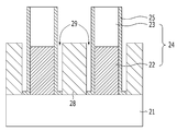
도 1은 일실시예에 따른 반도체장치를 도시한 도면이다.1 is a view showing a semiconductor device according to an embodiment.
도 1을 참조하면, 기판(101) 상에 복수의 반도체구조물이 형성된다. 반도체구조물은 도전구조물을 포함할 수 있다. 도전구조물은 제1도전구조물(104)과 제2도전구조물(110)을 포함할 수 있다. 제1도전구조물(104)과 제2도전구조물(110) 사이에는 에어갭(111)이 형성될 수 있다. 에어갭(111)의 상부에는 캡핑층(112)이 형성될 수 있다.Referring to FIG. 1, a plurality of semiconductor structures are formed on a
제1도전구조물(104)은 제1도전층(102)을 포함할 수 있다. 제1도전구조물(104)은 제1도전층(102)과 하드마스크층(103)을 포함하는 적층구조일 수 있다. 제1도전층(102)은 실리콘함유층, 금속함유층을 포함할 수 있다. 제1도전층(102)은 실리콘함유층과 금속함유층이 적층될 수 있다. 제1도전층(102)은 폴리실리콘, 금속, 금속질화물, 금속실리사이드 등을 포함할 수 있다. 제1도전층(102)은 폴리실리콘층과 금속층이 적층될 수 있다. 금속층은 텅스텐을 포함할 수 있다. 하드마스크층(103)은 절연물질을 포함할 수 있다. 하드마스크층(103)은 산화물 또는 질화물을 포함할 수 있다. 제1도전구조물(104)과 제2도전구조물(110) 중 어느 하나의 도전구조물은 어느 한 방향으로 연장된 라인 형상(Line type)을 가질 수 있다. 다른 하나의 도전구조물은 플러그 형상을 가질 수 있다. 예를 들어, 제1도전구조물(104)은 라인형상의 구조물이고, 제2도전구조물(110)은 플러그 형상의 구조물일 수 있다. 제1도전구조물(104)은 기판(101) 상에서 일정한 간격을 가지면서 규칙적으로 배치될 수 있다. 제2도전구조물(110)은 제1도전구조물(104) 사이에 형성된 오픈부에 형성될 수 있다. 오픈부는 콘택홀 등을 포함할 수 있다.The first
제2도전구조물(110)은 제1도전구조물(104) 사이에 리세싱된 제2도전층(106)을 포함할 수 있다. 제2도전구조물(110)은 제2도전층(106), 보호층(107), 오믹콘택층(108) 및 제3도전층(109)을 포함하는 적층구조일 수 있다. 제2도전층(106)과 보호층(107)은 실리콘함유층을 포함할 수 있다. 제2도전층(106)과 보호층(107)은 폴리실리콘층을 포함할 수 있다. 오믹콘택층(108)과 제3도전층(109)은 금속함유층을 포함할 수 있다. 오믹콘택층(108)은 코발트실리사이드 등의 금속실리사이드를 포함할 수 있다. 제3도전층(109)은 금속, 금속실리사이드, 금속질화물 등을 포함할 수 있다. 제3도전층(109)은 배리어층과 금속층의 적층구조일 수 있다. 제3도전층(109)은 티타늄질화물과 텅스텐을 적층하여 형성할 수 있다.The second
캡핑층(112)은 에어갭(111)을 캡핑하는 형태일 수 있다. 캡핑층(112)은 제2도전층(106)의 산화물을 포함할 수 있다. 특히, 캡핑층(112)은 제2도전층(106)의 플라즈마산화물을 포함할 수 있다. 캡핑층(112)은 실리콘산화물을 포함할 수 있다.The
제1도전구조물(104)의 양측벽에는 스페이서(105)가 형성될 수 있다. 스페이서(105)는 절연물질을 포함할 수 있다. 스페이서(105)는 산화물 또는 질화물을 포함할 수 있다. 스페이서(105)는 에어갭(111)과 함께 제1도전구조물(104)과 제2도전구조물(110) 사이의 절연 역할을 할 수 있다.
제1도전구조물(104)과 제2도전구조물(110) 중 어느 하나는 게이트, 비트라인을 포함할 수 있다. 다른 하나는 콘택플러그를 포함할 수 있다. 콘택플러그는 스토리지노드콘택플러그, 랜딩플러그 등을 포함할 수 있다. 도 1에서, 제1도전구조물(104)의 제1도전층(102)는 비트라인을 포함할 수 있고, 제2도전구조물(110)은 스토리지노드콘택플러그를 포함할 수 있다. 따라서, 비트라인과 스토리지노드콘택플러그 사이에 에어갭(111)이 형성될 수 있다. 제2도전층(106)은 제1플러그가 될 수 있고, 제3도전층(109)은 제2플러그가 될 수 있다. 제1플러그가 실리콘함유층을 포함하고, 제2플러그가 금속함유층을 포함하므로, 스토리지노드콘택플러그는 실리콘함유플러그와 금속함유플러그의 적층구조가 될 수 있다.Either the first
도 1에 도시된 바와 같이, 제1도전구조물(104)과 제2도전구조물(110) 사이에 에어갭(111)이 형성된다. 에어갭(111)은 유전율이 1로서 제1도전구조물(104)과 제2도전구조물(110)간의 기생캐패시턴스를 감소시킨다. 또한, 에어갭(111)의 상부는 캡핑층(112)에 의해 밀폐된다.As shown in FIG. 1, an
에어갭(111)을 캡핑하는 캡핑층(112)으로서 제2도전층(106)을 산화시킨 산화물로 형성하고 캡핑층(112) 및 제2도전층(106) 상에 보호층(107)을 형성하므로써, 캡핑층(112)을 보호하여 에어갭(111)을 안정적으로 캡핑할 수 있다. 실리사이드화가 가능한 물질을 이용하여 보호층(107)을 형성하고, 보호층(107) 상에 오믹콘택층(108)을 형성하므로써 오믹콘택층(108)의 형성 면적을 증가시킬 수 있다.A
도 1에 따른 반도체장치는 보호층(107)을 이용하여 캡핑층(112)의 어택을 방지하므로써 에어갭(29)을 안정적으로 구현할 수 있다. 또한, 보호층(107) 상에 오믹콘택층(108)을 형성하므로써 콘택저항을 개선시킬 수 있다.The semiconductor device according to FIG. 1 can reliably realize the
도 2a 내지 도 2o는 일실시예에 따른 반도체장치를 형성하는 방법의 일예를 나타낸 도면이다.2A to 2O are views showing an example of a method of forming a semiconductor device according to an embodiment.
도 2a에 도시된 바와 같이, 기판(21) 상에 복수의 제1도전구조물(24)을 형성한다. 기판(21)은 실리콘을 함유할 수 있다. 기판(21)은 실리콘기판, 실리콘저마늄기판을 포함할 수 있다. 또한, 기판(21)은 SOI 기판을 포함할 수도 있다. A plurality of first
기판(21) 상에 형성되는 제1도전구조물(24)은 일정 간격을 가지면서 규칙적으로 배치되는 라인 형상을 가질 수 있다. 제1도전구조물(24)을 형성하기 위해 제1도전층 상에 하드마스크패턴(23)을 형성한다. 하드마스크패턴(23)을 식각 마스크로 사용하여 제1도전층을 식각하므로써 제1도전층패턴(22)이 형성된다. 제1도전층패턴(22)과 하드마스크패턴(23)이 적층된 제1도전구조물(24)이 형성된다. 제1도전층패턴(22)은 실리콘함유층, 금속함유층을 포함할 수 있다. 예를 들어, 제1도전층패턴(22)은 폴리실리콘층 또는 텅스텐층을 포함할 수 있다. 또한, 제1도전층패턴(22)은 폴리실리콘층과 금속층을 적층하여 형성할 수 있으며, 이때, 폴리실리콘층과 금속층 사이에 배리어층이 더 형성될 수 있다. 제1도전층패턴(22)은 폴리실리콘층, 티타늄함유층 및 텅스텐층의 적층구조물을 포함할 수 있다. 티타늄함유층은 배리어층으로서, 티타늄층과 티타늄질화물이 적층될 수 있다.The first
도 2b에 도시된 바와 같이, 제1도전구조물(24)을 포함한 전면에 절연층(25A)을 형성한다. 절연층(25A)은 질화물 또는 산화물을 포함할 수 있다. 절연층(25A)은 실리콘질화물, 실리콘산화물을 포함할 수 있다. 절연층(25A)은 스페이서가 되는 물질이다.As shown in FIG. 2B, the insulating
절연층(25A) 상에 희생층(26A)을 형성한다. 희생층(26A)은 후속 공정에서 제거되어 에어갭을 형성하는 물질이다. 희생층(26A)은 절연층(25A)과 식각선택비를 갖는 물질을 포함할 수 있다. 희생층(26A)은 산화물, 질화물, 금속질화물을 포함할 수 있다. 절연층(25A)이 산화물을 포함하는 경우, 희생층(26A)은 금속질화물 또는 질화물을 포함할 수 있다. 절연층(25A)이 질화물을 포함하는 경우, 희생층(26A)은 산화물 또는 금속질화물을 포함할 수 있다. 희생층(26A)은 실리콘산화물, 실리콘질화물, 티타늄질화물(TiN)을 포함할 수 있다.A
도 2c에 도시된 바와 같이, 제1도전구조물(24)의 양측벽에 이중 스페이서(Double spacer)를 형성한다. 이중 스페이서는 스페이서(25)와 희생스페이서(26)를 포함할 수 있다. 스페이서(25)는 절연층(25A)을 식각하므로써 형성될 수 있다. 스페이서(25)의 측벽에는 희생스페이서(26)가 형성될 수 있다. 희생스페이서(26)는 희생층(26A)을 식각하므로써 형성될 수 있다. 스페이서(25)와 희생스페이서(26)를 형성하기 위해, 에치백 공정이 적용될 수 있다.As shown in FIG. 2C, a double spacer is formed on both side walls of the first
이와 같이, 스페이서(25)과 희생스페이서(26)를 형성하므로써 제1도전구조물(24) 사이에 기판(21)을 노출시키는 오픈부(27)가 형성될 수 있다. 다른 실시예에서, 스페이서(25)를 형성한 후 층간절연층(미도시)을 형성하고, 층간절연층을 식각하여 오픈부(27)를 형성할 수도 있다. 오픈부(27) 형성후에, 오픈부(27)의 측벽에 희생스페이서(26)를 형성할 수도 있다.The
오픈부(27)는 희생스페이서(26)의 측벽을 노출시키면서 형성될 수 있다. 오픈부(27)는 라인 형상을 갖거나, 콘택홀 형상을 가질 수 있다. 예를 들어, 제1도전구조물(24)이 비트라인구조물을 포함하는 경우, 오픈부(27)는 스토리지노드콘택홀을 포함할 수 있다.The
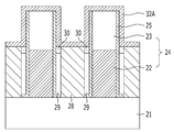
도 2d에 도시된 바와 같이, 오픈부(27)를 갭필하는 제2도전층(28A)을 형성한다. 제2도전층(28A)은 실리콘함유층을 포함할 수 있다. 제2도전층(28A)은 폴리실리콘층을 포함할 수 있다.As shown in FIG. 2D, a second
도 2e에 도시된 바와 같이, 제2도전층(28A)을 선택적으로 제거한다. 이에 따라, 제1도전구조물(24) 사이에 리세스된 제2도전층패턴(28)이 형성된다. 제2도전층패턴(28)을 형성하기 위해 에치백 공정이 적용될 수 있다. 제2도전층패턴(28)은 제1도전구조물(24)의 표면보다 낮게 리세스된 표면을 갖는다. 제2도전층패턴(28)의 리세스된 표면은 적어도 제1도전층패턴(22)의 상부 표면보다 높게 제어할 수 있다. 제2도전층패턴(28)의 높이는 제1도전층패턴(22)과의 대향면적을 최소화시키는 높이를 가질 수 있다. 이로써, 제1도전층패턴(22)와 제2도전층패턴(28)간의 기생캐패시턴스를 감소시킬 수 있다. 제2도전층패턴(28)은 콘택플러그가 될 수 있다. 제1도전구조물(24)이 비트라인구조물을 포함하는 경우, 제2도전층패턴(28)은 스토리지노드콘택플러그의 일부가 될 수 있다. 제2도전층패턴(28)을 형성할 때, 스페이서(25)와 희생스페이서(26)는 선택비를 가져 식각되지 않는다.As shown in FIG. 2E, the second
도 2f에 도시된 바와 같이, 희생스페이서(26)를 선택적으로 제거한다. 이에 따라, 에어갭(29)이 형성된다. 에어갭(29)은 제2도전층패턴(28)의 측벽에 형성될 수 있다. 제2도전층패턴(28)과 제1도전층패턴(22) 사이에 에어갭(29)이 형성된다. 제1도전층패턴(22)과 제2도전층패턴(28) 사이에는 '에어갭(29)-스페이서(25)'의 절연구조가 형성된다.As shown in FIG. 2F, the
희생스페이서(26)를 제거하기 위해 습식식각(Wet Etch) 또는 건식식각(Dry Etch)이 적용될 수 있다. 희생스페이서(26)를 제거할 때, 스페이서(25), 제2도전층패턴(28) 및 하드마스크패턴(23)은 선택비를 가져 손상되지 않는다. 희생스페이서(26)가 티타늄질화물인 경우, H2SO4와 H2O2가 혼합된 용액을 이용한 습식세정을 진행할 수 있다.Wet Etch or Dry Etch may be applied to remove the
위와 같이, 에어갭(29)을 형성하므로써 제1도전층패턴(22)과 제2도전층패턴(28) 사이의 기생캐패시턴스가 감소한다.As described above, parasitic capacitance between the first
도 2g에 도시된 바와 같이, 제2도전층패턴(28)의 상부 표면과 측벽에 캡핑층(30A)을 형성한다. 캡핑층(30A)은 절연물질을 포함할 수 있다. 캡핑층(30A)은 제2도전층패턴(28)의 산화물을 포함할 수 있다. 캡핑층(30A)은 실리콘산화물을 포함할 수 있다. 캡핑층(30A)은 산화 공정을 통해 형성할 수 있다. 제2도전층패턴(28)이 실리콘함유층을 포함하므로, 산화공정에 의해 제2도전층패턴(28)의 상부와 측벽에 실리콘산화물이 형성될 수 있다. 캡핑층(30A)은 에어갭(29)의 입구를 막는 두께로 형성할 수 있다. 캡핑층(30A)은 플라즈마산화법을 이용하여 형성할 수 있다. 이때, 에어갭(29)의 입구를 막을 수 있는 두께로 형성한다. 플라즈마산화법을 이용하여 캡핑층(30A)을 형성하면, 제2도전층패턴(28)의 상부 표면에서 산화됨과 동시에 제2도전층패턴(28)의 상부 모서리에서 빠르게 산화가 진행된다. 이와 같이 플라즈마산화법을 이용함에 따라, 제2도전층패턴(28)의 하부 측벽에서는 산화가 거의 발생하지 않기 때문에, 제2도전층패턴(28)을 덮는 캡핑층(30A)을 선택적으로 형성할 수 있다.As shown in FIG. 2G, a
캡핑층(30A)을 형성하므로써 후속 공정시 에어갭(29)이 오픈되는 것을 방지할 수 있다.By forming the
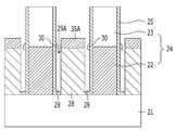
도 2h에 도시된 바와 같이, 캡핑층(30A)을 선택적으로 제거하여 제2도전층패턴(28)의 상부 표면을 노출시킨다. 이에 따라, 제2도전층패턴(28)의 상부 측벽에 도면부호 '30'과 같은 캡핑층(30)이 잔류한다. 캡핑층(30)은 에어갭(29)을 캡핑하고, 제2도전층패턴(28)의 상부 표면을 노출시킨다. 캡핑층(30)을 잔류시키기 위해 습식식각이 적용될 수 있다. 캡핑층(30)이 실리콘산화물을 포함하므로, 불산계 케미컬을 이용할 수 있다.The
도 2i에 도시된 바와 같이, 이온주입(31)을 실시한다. 이온주입(31)은 제2도전층패턴(28)에 실시할 수 있다. 이로써, 콘택저항을 개선시킬 수 있다. 이온주입(31)은 N형 도펀트 또는 P형 도펀트를 주입할 수 있다. 이러한 이온주입(31)은 후속 보호층(32A) 형성 이후에 진행할 수도 있다.As shown in FIG. 2I, an
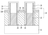
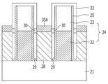
도 2j에 도시된 바와 같이, 보호층(32A)을 형성한다. 즉, 제2도전층패턴(28), 캡핑층(30) 및 제1도전구조물(24)을 포함한 전면에 보호층(32A)을 컨포멀하게(Conformally) 형성한다. 보호층(32A)은 도전물질을 포함할 수 있다. 보호층(32A)은 실리콘함유층을 포함할 수 있다. 보호층(32A)은 실리사이드화가 가능한 물질, 즉 제1실리사이드화가능물질을 포함할 수 있다. 보호층(32A)으로서 폴리실리콘층이 형성될 수 있다. 보호층(32A)을 형성하면, 제2도전층패턴(28)과 함께 이중 구조의 폴리실리콘층 구조가 형성될 수 있다. 보호층(32A)의 두께는 후속 실리사이드화반응이 일어나더라도 일정 두께의 보호층(32A)이 잔류하도록 조절할 수 있다.As shown in Fig. 2J, a
도 2k에 도시된 바와 같이, 보호층(32A)을 선택적으로 제거한다. 이를 위해 에치백 공정이 수행될 수 있다. 에치백 공정에 의해 제2도전층패턴(28)과 캡핑층(30) 상에 보호층(32B)이 잔류한다. 보호층(32B)은 후속 공정에서 캡핑층(30)의 손실을 방지하여 에어갭(29)을 안정적으로 캡핑할 수 있다.As shown in FIG. 2K, the
도 2l에 도시된 바와 같이, 보호층(32B)을 포함한 전면에 제2실리사이드화가능물질(33)과 산화방지층(34)을 형성한다. 제2실리사이드화물질(33)은 실리사이드화가능금속층을 포함할 수 있다. 제2실리사이드화가능물질(33)은 코발트를 포함할 수 있다. 산화방지층(34)은 후속 실리사이드화반응 공정동안 제2실리사이드화가능물질이 산화되는 것을 방지한다. 산화방지층(34)은 티타늄층과 티타늄질화물을 적층하여 형성할 수 있다.As shown in FIG. 21, a
도 2m에 도시된 바와 같이, 오믹콘택층(35)을 형성한다. 오믹콘택층(35)은 금속실리사이드를 포함할 수 있다. 오믹콘택층(35)을 형성하기 위해 어닐을 실시할 수 있다. 어닐에 의해 제2실리사이드화가능물질(33)의 금속과 보호층(32B)의 실리콘이 반응하여 금속실리사이드가 형성될 수 있다. 금속실리사이드는 코발트실리사이드를 포함할 수 있다. 본 실시예에서, 금속실리사이드는 'CoSi2 상'의 코발트실리사이드를 포함할 수 있다. 금속실리사이드로서 CoSi2상의 코발트실리사이드를 형성하므로써 콘택저항을 개선시킴과 동시에 미세 선폭을 갖는 오픈부(27)의 작은 면적에서도 충분히 저저항의 코발트실리사이드를 형성할 수 있다. 보호층(32B)과 제2실리사이드화가능물질(33)이 반응하여 금속실리사이드가 형성되므로, 금속실리사이드의 형성 면적을 증가시킬 수 있다. 결국, 오믹콘택층(35)의 형성 면적이 증가하여 콘택저항을 개선시킬 수 있다. 또한, 보호층(32B)을 버퍼로 하여 금속실리사이드를 형성하므로, 금속실리사이드가 제2도전층패턴(28)으로 확산하는 것을 방지할 수 있다.An
오믹콘택층(35)을 형성한 후에 보호층은 도면부호 '32'와 같이 일정 두께를 갖고 잔류할 수 있다. 또한, 미반응된 제2실리사이드화가능물질은 도면부호 '33A'와 같이 잔류할 수 있다.After forming the
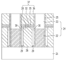
도 2n에 도시된 바와 같이, 산화방지층(34)을 제거한 후 미반응하고 잔류하는 제2실리사이드화물질(33A)을 제거한다. 미반응 제2실리사이드화가능물질(33A)을 제거하지 않으면, 후속 공정에서 미반응 제2실리사이드화가능물질(33A)의 금속원자가 하부로 확산하거나, 금속실리사이드의 이상 반응을 일으킬 수 있다. 따라서, 미반응 제2실리사이드화가능물질(33A)을 제거한다. 미반응 제2실리사이드화가능물질(33A)은 습식케미컬을 이용한 세정 공정을 통해 제거할 수 있다. 예를 들어, 미반응 제2실리사이드화가능물질(33A)이 코발트인 경우, H2SO4(SPM)과 NH4OH(SC-1) 계열의 케미컬을 이용할 수 있다. 부연하면, 탈이온수(DI Water)를 이용하여 미반응 코발트를 산화시키고, H2SO4(SPM)과를 이용하여 1차 제거를 하고, 잔류하는 금속성폴리머 계열의 잔류물(Residue)을 NH4OH 계열의 케미컬을 이용하여 2차 제거한다. 습식케미컬을 이용하므로써 미반응 코발트층은 물론 금속성 폴리머를 깨끗하게 제거할 수 있다.As shown in FIG. 2N, after removing the
상술한 바와 같이, 미반응 제2실리사이드화가능물질(33A)을 스트립할 때, 보호층(32)에 의해 캡핑층(30) 및 에어갭(29)이 보호될 수 있다.As described above, the
도 2o에 도시된 바와 같이, 오믹콘택층(35) 상에 제3도전층패턴(36)을 형성할 수 있다. 제3도전층패턴(36)를 형성하기 위해 오믹콘택층(35)의 상부를 갭필하는 제3도전층을 형성한 후, 평탄화 공정을 진행할 수 있다. 제3도전층패턴(36)은 금속함유층을 포함할 수 있다. 제3도전층패턴(36)는 텅스텐층을 포함할 수 있다. 도시하지 않았으나, 제3도전층패턴(36)은 배리어층을 더 포함할 수 있다. 따라서, 제3도전층패턴(36)는 배리어층과 금속함유층을 적층하여 형성할 수 있다. 배리어층은 티타늄을 함유하는 물질을 포함할 수 있다. 배리어층은 티타늄을 단독으로 형성하거나 또는 티타늄과 티타늄질화물을 적층하여 형성할 수 있다.The third
위와 같이, 제3도전층패턴(36)를 형성하면, 제2도전층패턴(28), 보호층(32), 오믹콘택층(35) 및 제3도전층패턴(36)을 포함하는 제2도전구조물(37)이 형성된다. 제1도전구조물(24)과 제2도전구조물(37) 사이에는 에어갭(29)이 형성된다. 제2도전구조물(37)은 스토리지노드콘택플러그가 될 수 있다. 제2도전층패턴(28)은 스토리지노드콘택플러그의 하부 플러그(Bottom plug)가 되고, 제3도전층패턴(36)은 스토리지노드콘택플러그의 상부 플러그(Top plug)가 될 수 있다. 제2도전층패턴(28)이 실리콘함유층을 포함하고, 제3도전층패턴(36)이 금속함유층을 포함하므로, 실리콘함유층과 금속함유층을 포함하는 콘택플러그, 즉, 세미메탈 콘택플러그 구조가 형성될 수 있다.As described above, when the third
에어갭(29)은 제1도전층패턴(22)과 제2도전층패턴(28) 사이에 형성될 수 있다. 제1도전층패턴(22)이 비트라인을 포함하고, 제2도전층패턴(28)이 스토리지노드콘택플러그를 포함하는 경우, 비트라인과 스토리지노드콘택플러그 사이에 에어갭(29)이 형성될 수 있다. 제1도전층패턴(22)이 게이트전극을 포함하고, 제2도전층패턴(28)이 콘택플러그를 포함하는 경우, 에어갭(29)은 게이트전극과 콘택플러그 사이에 형성될 수 있다.The
도 3a 및 도 3b는 일실시예의 비교예1를 설명하기 위한 도면이다.3A and 3B are views for explaining Comparative Example 1 of one embodiment.
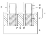
도 3a 및 도 3b를 참조하면, 기판(11) 상에 제1도전층(12)과 하드마스크층(13)이 적층된 복수의 제1도전구조물(14)이 형성되고, 제1도전구조물(14) 사이에 제2도전구조물의 제2도전층(16)이 형성된다. 제1도전구조물(14)와 제2도전층(16) 사이에 에어갭(17)이 형성된다. 제1도전구조물(14)의 측벽에 스페이서(15)가 형성된다.3A and 3B, a plurality of first
비교예1은 캡핑층(18)으로서 단독의 절연물질이 사용될 수 있다. 캡핑층(18)은 실리콘질화물 또는 실리콘산화물이 사용될 수 있다. 캡핑층(18)으로서 절연물질이 사용됨에 따라, 후속 공정을 위해 제2도전층(16)의 표면으로부터 캡핑층(18)이 선택적으로 제거되어야 한다.In Comparative Example 1, a single insulating material may be used as the
그러나, 캡핑층(18)이 후속 공정에 의하여 어택을 받을 경우 자기정렬콘택페일(SAC Fail)이 발생하며, 안정적인 에어갭(17)을 형성하기 위하여 캡핑층(18)을 두껍게 형성할 경우에는 금속실리사이드의 형성 면적이 매우 적어져 콘택저항이 크게 증가한다.However, when the
특히, 캡핑층(18)을 단독으로 형성할 경우 금속실리사이드 형성을 위하여 제2도전층(16)의 상부를 오픈시키기 위하여 캡핑층(18)을 식각할 때에, 캡핑층(18)에 어택을 주어 에어갭(17)이 오픈되는 문제가 발생한다(도면부호 '19' 참조).Particularly, when the
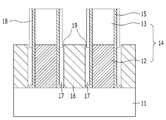
도 4a 내지 도 4c는 일실시예의 비교예2를 설명하기 위한 도면이다.4A to 4C are views for explaining Comparative Example 2 of one embodiment.
도 4a를 참조하면, 제2도전층패턴(28)의 상부 표면이 노출되도록 하여 캡핑층(30)을 잔류시킨다(도 2h 참조).Referring to FIG. 4A, the upper surface of the second
다음으로, 코발트층(33)을 전면에 증착한 후, 어닐을 실시하여 코발트실리사이드(35A)를 형성한다. 어닐에 의해 제2도전층패턴(28)과 코발트층(33)이 반응하여 코발트실리사이드(35A)가 형성된다.Next, after the
도 4b를 참조하면, 미반응하고 잔류하는 코발트층(33)을 스트립한다. Referring to FIG. 4B, unreacted and remaining
그러나, 비교예2는 미반응 코발트층을 스트립할 때, 캡핑층(30)이 어택받아 손실될 수 있고, 이로써, 에어갭(29)이 오픈되는 문제(도면부호 '29A' 참조)가 발생한다. 비교예2에 의해서는 안정적으로 에어갭(29)을 캡핑하기 어렵다. 또한, 비교예2는 보호층없이 제2도전층패턴(28)과 코발트층(33)을 직접 반응시키므로 코발트실리사이드(35A)의 형성 면적이 작아진다.However, in Comparative Example 2, when the unreacted cobalt layer is stripped, the
캡핑층(30)의 어택을 방지하기 위해 도 4c에 도시된 바와 같이, 코발트층을 증착하기 전에 절연성 캡핑층(38)을 더 형성할 수도 있으나, 이 경우에는 코발트실리사이드(35A)의 형성 면적이 작아져 콘택저항이 크게 증가한다. 즉, 캡핑층(30)을 보호하기 위해 두꺼운 절연성 캡핑층(38)을 형성해야 하고, 이로써 오픈부의 상부 선폭(도면부호 'CD' 참조)이 감소할 수 밖에 없다. 결국, 제2도전층패턴(28)과 반응하는 코발트층(33)의 접촉면적이 작아지기 때문에 면적이 작은 코발트실리사이드(35A)가 형성될 수 밖에 없다. 이로써 제2도전층패턴(28)과 오믹콘택층인 코발트실리사이드(35A)간의 접촉면적이 작아져 콘택저항을 개선시키는데 한계가 있다.In order to prevent the attack of the
결국, 본 실시예들과 같이, 캡핑층(30) 상에 보호층(32)을 형성하므로써 후속 공정에서 에어갭(29)을 안정적으로 캡핑할 수 있다. 또한, 보호층(32)과의 반응을 통해 오믹콘택층(35)을 형성하므로 콘택저항을 개선시킬 수 있다.As a result, by forming the
도 5a는 DRAM의 메모리셀을 도시한 배치도이고, 도 5b는 도 5a의 A-A'선에 따른 단면도이다. 도 5c는 도 5a의 B-B'선에 따른 단면도이다.5A is a layout diagram showing a memory cell of a DRAM, and FIG. 5B is a cross-sectional view taken along line A-A 'of FIG. 5A. 5C is a cross-sectional view taken along the line B-B 'in FIG. 5A.
도 5a, 도 5b 및 도 5c를 참조하면, 기판(41)에 소자분리영역(42)에 의해 활성영역(43)이 정의된다. 활성영역(43)과 소자분리영역(42)을 가로지르는 트렌치(44)에 매립게이트전극(46)이 형성된다. 매립게이트전극(46)과 교차하는 방향으로 연장된 비트라인(51)이 기판(41) 상부에 형성되며, 비트라인(51)은 비트라인콘택플러그(50)를 통해 활성영역(43)과 연결된다. 활성영역(43)에 연결되는 스토리지노드콘택플러그가 형성된다. 스토리지노드콘택플러그는 제1스토리지노드콘택플러그(56), 보호층(59), 오믹콘택층(60) 및 제2스토리지노드콘택플러그(61)가 적층될 수 있다. 제2스토리지노드콘택플러그(61) 상에 캐패시터의 스토리지노드(62)가 형성된다.Referring to Figs. 5A, 5B, and 5C, the
스토리지노드콘택플러그는 본 실시예들에 따른 제2도전구조물에 대응할 수 있고, 비트라인은 제1도전구조물의 제1도전층패턴에 대응할 수 있다. 따라서, 제1스토리지노드콘택플러그(56)와 비트라인(51) 사이에 에어갭(58)이 형성될 수 있다. 보호층(59)은 폴리실리콘층을 포함하고, 오믹콘택층(60)은 금속실리사이드를 포함할 수 있다.The storage node contact plug may correspond to the second conductive structure according to the embodiments, and the bit line may correspond to the first conductive layer pattern of the first conductive structure. Thus, an
에어갭(58)은 캡핑층(57)에 의해 캡핑되고, 캡핑층(57) 및 제1스토리지노드콘택플러그(56) 상에 보호층(59)이 형성된다. 캡핑층(57)은 본 실시예들에 따른 제캡핑층에 대응될 수 있고, 따라서, 캡핑층(57)은 실리콘산화물을 포함할 수 있다. 보호층(59)은 본 실시예들에 따른 보호층에 대응할 수 있고, 따라서, 폴리실리콘층을 포함할 수 있다. 오믹콘택층(60)은 코발트실리사이드를 포함할 수 있다.The
도 5a, 도 5b 및 도 5c를 참조하여 메모리셀의 제조 방법을 살펴보면 다음과 같다.A method of manufacturing a memory cell will be described with reference to FIGS. 5A, 5B, and 5C.
기판(41)은 반도체 물질을 포함할 수 있다. 기판(41)은 반도체기판을 포함할 수 있다. 기판(41)은 실리콘 기판을 포함할 수 있으며, 예를 들어, 단결정 실리콘 기판을 포함할 수 있다. 소자분리영역(42)은 STI(Shallow Trench Isolation) 공정을 통해 형성할 수 있다. 소자분리영역(42)에 의해 활성영역(43)이 정의될 수 있다. 소자분리영역(42)은 측벽산화물(Wall oxide), 라이너(liner) 및 갭필물질(Gapfill material)을 순차적으로 형성할 수 있다. 라이너는 실리콘질화물(Silicon nitride), 실리콘산화물(Silicon oxide)을 포함할 수 있다. 실리콘질화물은 Si3N4를 포함할 수 있고, 실리콘산화물은 SiO2를 포함할 수 있다. 갭필물질은 스핀온절연물(SOD) 등의 실리콘산화물을 포함할 수 있다. 또한, 갭필물질은 실리콘질화물을 포함할 수 있으며, 이때, 실리콘질화물은 라이너로 사용되는 실리콘질화물을 이용하여 갭필할 수 있다.The
트렌치(44)는 활성영역(43)과 소자분리영역(42)에서 동시에 형성될 수 있다. 활성영역(43)과 소자분리영역(42)의 식각률 차이에 의해 소자분리영역(42)에서 더 깊게 형성될 수 있다.The
매립게이트전극(46)을 형성하기 전에 트렌치(44)의 표면에 게이트절연층(45)을 형성할 수 있다. 매립게이트전극(46)은 트렌치(44)를 갭필하도록 금속함유층을 형성한 후 에치백하여 형성할 수 있다. 금속함유층은 티타늄, 탄탈륨, 텅스텐 등의 금속을 주성분으로 하는 물질을 포함할 수 있다. 금속함유층은 탄탈륨질화물(TaN), 티타늄질화물(TiN), 텅스텐질화물(WN) 및 텅스텐(W)으로 이루어진 그룹 중에서 선택된 적어도 어느 하나를 포함할 수 있다. 예를 들어, 매립게이트전극(46)은 티타늄질화물, 탄탈륨질화물 또는 텅스텐을 단독으로 포함하거나, 티타늄질화물(TiN) 또는 탄탈륨질화물(TaN) 상에 텅스텐(W)을 적층하는 TiN/W 또는 TaN/W과 같은 2층 구조로 형성할 수 있다. 또한, 텅스텐질화물(WN) 상에 텅스텐(W)을 적층하는 WN/W의 2층 구조를 포함할 수 있으며, 이 외에 낮은 저항의 금속물질을 포함할 수 있다.The
매립게이트전극(46) 상에 실링층(Sealing layer, 47)을 형성한다. 실링층(47)은 매립게이트전극(46) 상에서 트렌치(44)를 갭필할 수 있다. 실링층(47)은 후속 공정으로부터 매립게이트전극(46)을 보호하는 역할을 수행할 수 있다. 실링층(47)은 절연물질을 포함할 수 있다. 실링층(47)은 실리콘질화물을 포함할 수 있다.A
제1층간절연층(48)을 형성한 후 제1층간절연층(48)과 실링층(47)을 식각하여 비트라인콘택홀(49)을 형성한다. 비트라인콘택홀(49)에 도전층을 형성하여 비트라인콘택플러그(50)를 형성한다. 비트라인콘택플러그(50) 상에 비트라인(51)과 비트라인하드마스크층(52)을 포함하는 비트라인구조물을 형성한다. 비트라인콘택플러그(50)는 폴리실리콘층 또는 금속함유층을 포함할 수 있다. 비트라인(51)은 텅스텐층을 포함할 수 있고, Ti/TiN 등의 배리어층과 배리어층 상의 텅스텐층을 포함할 수도 있다. 비트라인하드마스크층(62)은 실리콘질화물을 포함할 수 있다.After forming the first
비트라인구조물의 양측벽에 스페이서(53)를 형성한다. 이후 제2층간절연층(54)을 형성한 후, 제2층간절연층(54), 제1층간절연층(48) 및 실링층(47)을 식각하여 스토리지노드콘택홀(55)을 형성한다. 스토리지노드콘택홀(55)의 측벽에 희생스페이서(도시 생략)를 형성한 후, 스토리지노드콘택홀(55)에 제1스토리지노드콘택플러그(56)를 리세싱시킨다. 이후, 희생스페이서를 제거하여 에어갭(58)을 형성한다.Spacers (53) are formed on both sidewalls of the bit line structure. After forming the second
다음으로, 제1스토리지노드콘택플러그(56)의 표면을 산화시켜 캡핑층(57)을 형성하고, 제1스토리지노드콘택플러그(56)의 표면이 노출되도록 캡핑층(57)을 선택적으로 제거한다. 캡핑층(57)에 의해 에어갭(58)이 캡핑된다. Next, the surface of the first storage
제1스토리지노드콘택플러그(56) 및 캡핑층(57) 상에 보호층(59)을 형성한다. 보호층(59)은 폴리실리콘층을 포함할 수 있다.A
보호층(59) 상에 오믹콘택층(60)을 형성한다. 오믹콘택층(60)은 보호층(59)상에 실리사이드화가능금속층을 형성한 후 어닐하여 형성할 수 있다. 오믹콘택층(60)은 금속실리사이드를 포함할 수 있다. 오믹콘택층(60)은 코발트실리사이드를 포함한다. An
오믹콘택층(60) 상에 제2스토리지노드콘택플러그(61)를 형성한다. 제2스토리지노드콘택플러그(61)는 금속함유층을 포함할 수 있다. 제2스토리지노드콘택플러그(61)은 텅스텐층을 포함할 수 있다.A second storage
제2스토리지노드콘택플러그(61) 상에 캐패시터의 스토리지노드(62)를 형성한다. 스토리지노드(62)는 실린더형태일 수 있고, 다른 실시예에서 필라 형태를 가질 수도 있다. 도시하지 않았지만, 스토리지노드(62) 상에 유전층 및 플레이트노드를 더 형성할 수 있다.Thereby forming the
상술한 실시예들에 따른 반도체장치는 DRAM(Dynamic Random Access Memory)에 적용될 수 있으며, 이에 한정되지 않고 SRAM(Static Random Access Memory), 플래시메모리(Flash Memory), FeRAM(Ferroelectric Random Access Memory), MRAM(Magnetic Random Access Memory), PRAM(Phase Change Random Access Memory) 등의 메모리에 적용될 수 있다.The semiconductor device according to the above-described embodiments may be applied to a dynamic random access memory (DRAM), and the present invention is not limited thereto. For example, a static random access memory (SRAM), a flash memory, a ferroelectric random access memory (FeRAM) (Magnetic Random Access Memory), and a PRAM (Phase Change Random Access Memory).
도 6은 메모리 카드를 보여주는 개략도이다. 6 is a schematic view showing a memory card;
도 6을 참조하면, 메모리 카드(200)는 제어기(210) 및 메모리(220)를 포함할 수 있다. 제어기(210) 및 메모리(220)는 전기적인 신호를 교환할 수 있다. 예를 들면, 제어기(210)의 명령에 따라서 메모리(220) 및 제어기(210)는 데이터를 주고받을 수 있다. 이에 따라, 메모리 카드(200)는 메모리(220)에 데이터를 저장하거나 또는 메모리(220)로부터 데이터를 외부로 출력할 수 있다. 메모리(220)는 앞서 설명한 바와 같은 에어갭 및 플러그들을 포함할 수 있다. 이러한 메모리 카드(200)는 다양한 휴대용 기기의 데이터 저장 매체로 이용될 수 있다. 예를 들면, 메모리 카드(200)는 메모리 스틱 카드(memory stick card), 스마트 미디어 카드(smart media card, SM), 씨큐어 디지털 카드(secure digital, SD), 미니 씨큐어 디지털 카드(mini secure digital card, mini SD), 또는 멀티 미디어 카드(multi media card, MMC) 등을 포함할 수 있다.Referring to FIG. 6, the
도 7는 전자 시스템을 보여주는 블록도이다. 7 is a block diagram showing an electronic system.
도 7을 참조하면, 전자 시스템(300)은 프로세서(310), 입/출력 장치(330) 및 칩(320)을 포함할 수 있고, 이들은 버스(340)를 이용하여 서로 데이터 통신을 할 수 있다. 프로세서(310)는 프로그램을 실행하고, 전자 시스템(300)을 제어하는 역할을 할 수 있다. 입/출력 장치(330)는 전자 시스템(300)의 데이터를 입력 또는 출력하는데 이용될 수 있다. 전자 시스템(300)은 입/출력 장치(330)를 이용하여 외부 장치, 예를 들면 개인용 컴퓨터 또는 네트워크에 연결되어, 외부 장치와 서로 데이터를 교환할 수 있다. 칩(320)은 프로세서(310)의 동작을 위한 코드 및 데이터를 저장할 수 있고, 프로세스(310)에서 주어지는 동작을 일부 처리할 수 있다. 예를 들면, 칩(320)은 앞서 설명한 에어갭 및 플러그들을 포함할 수 있다. 전자 시스템(300)은 칩(320)을 필요로 하는 다양한 전자 제어 장치를 구성할 수 있으며, 예를 들면 모바일 폰(mobile phone), MP3 플레이어, 네비게이션(navigation), 고상 디스크 (solid state disk: SSD), 가전 제품(household appliances) 등에 이용될 수 있다.7, the
전술한 본 발명은 전술한 실시예 및 첨부된 도면에 의해 한정되는 것이 아니고, 본 발명의 기술적 사상을 벗어나지 않는 범위 내에서 여러 가지 치환, 변형 및 변경이 가능하다는 것이 본 발명이 속하는 기술분야에서 통상의 지식을 가진 자에게 있어 명백할 것이다.It will be apparent to those skilled in the art that various modifications and variations can be made in the present invention without departing from the spirit or scope of the invention as defined by the appended claims. Will be clear to those who have knowledge of.
101 : 기판 102 : 제1도전층
103 : 하드마스크층 104 : 제1도전구조물
105 : 스페이서 106 : 제2도전층
107 : 보호층 108 : 오믹콘택층
109 : 제3도전층 110 : 제2도전구조물
111 : 에어갭 112 : 캡핑층101: substrate 102: first conductive layer
103: hard mask layer 104: first conductive structure
105: spacer 106: second conductive layer
107: protective layer 108: ohmic contact layer
109: third conductive layer 110: second conductive structure
111: air gap 112: capping layer
Claims (23)
상기 오픈부의 측벽에 희생스페이서를 형성하는 단계;
상기 오픈부에 리세스된 제1플러그를 형성하는 단계;
상기 희생스페이서를 제거하여 에어갭을 형성하는 단계;
상기 제1플러그의 상부표면을 노출시키고 상기 에어갭을 캡핑하는 캡핑층을 형성하는 단계;
상기 캡핑층 및 제1플러그 상에 보호층을 형성하는 단계;
상기 보호층 상에 오믹콘택층을 형성하는 단계; 및
상기 오믹콘택층 상에 제2플러그를 형성하는 단계
를 포함하는 반도체장치 제조 방법.
Forming a semiconductor structure having an open portion on a substrate;
Forming a sacrificial spacer on a sidewall of the open portion;
Forming a recessed first plug in the open portion;
Removing the sacrificial spacers to form an air gap;
Forming a capping layer exposing an upper surface of the first plug and capping the air gap;
Forming a protective layer on the capping layer and the first plug;
Forming an ohmic contact layer on the protective layer; And
Forming a second plug on the ohmic contact layer
≪ / RTI >
상기 캡핑층을 형성하는 단계는,
상기 제1플러그의 표면을 산화시켜 산화물을 형성하는 단계; 및
상기 제1플러그의 상부 표면이 노출되도록 상기 산화물을 선택적으로 제거하는 단계
를 포함하는 반도체장치 제조 방법.The method according to claim 1,
Wherein forming the capping layer comprises:
Oxidizing the surface of the first plug to form an oxide; And
Selectively removing the oxide so that the upper surface of the first plug is exposed;
≪ / RTI >
상기 제1플러그는 실리콘함유물질로 형성하고, 상기 캡핑층은 상기 실리콘함유물질의 산화물로 형성하는 반도체장치 제조 방법.
The method according to claim 1,
Wherein the first plug is formed of a silicon-containing material, and the capping layer is formed of an oxide of the silicon-containing material.
상기 제1플러그는 폴리실리콘층으로 형성하고, 상기 캡핑층은 상기 폴리실리콘층을 산화시킨 실리콘산화물로 형성하는 반도체장치 제조 방법.
The method according to claim 1,
Wherein the first plug is formed of a polysilicon layer and the capping layer is formed of silicon oxide oxidized in the polysilicon layer.
상기 보호층을 형성하는 단계는,
상기 캡핑층 및 제1플러그를 포함한 전면에 폴리실리콘층을 갭필하는 단계; 및
상기 폴리실리콘층을 에치백하는 단계
를 포함하는 반도체장치 제조 방법.
The method according to claim 1,
The step of forming the protective layer may include:
Capping a polysilicon layer over the entire surface including the capping layer and the first plug; And
Etching back the polysilicon layer
≪ / RTI >
상기 오믹콘택층을 형성하는 단계는,
상기 보호층 상에 실리사이드화가능금속층을 형성하는 단계;
어닐을 실시하여 상기 보호층과 실리사이드화가능금속층을 반응시켜 금속실리사이드를 형성하는 단계; 및
미반응 상기 실리사이드화가능금속층을 제거하는 단계
를 포함하는 반도체장치 제조 방법.
The method according to claim 1,
Wherein forming the ohmic contact layer comprises:
Forming a silicidizable metal layer on the protective layer;
Performing an anneal to react the protective layer and the silicidizable metal layer to form a metal silicide; And
Removing the unreacted metal silicide layer
≪ / RTI >
상기 실리사이드화금속층은, 코발트층을 포함하는 반도체장치 제조 방법.
The method according to claim 6,
Wherein the silicidation metal layer comprises a cobalt layer.
상기 제1플러그는 폴리실리콘층을 포함하고, 상기 제2플러그는 금속함유물질을 포함하는 반도체장치 제조 방법.
The method according to claim 1,
Wherein the first plug comprises a polysilicon layer and the second plug comprises a metal containing material.
상기 비트라인구조물 사이에 스토리지노드콘택홀을 형성하는 단계;
상기 스토리지노드콘택홀의 측벽에 희생스페이서를 형성하는 단계;
상기 스토리지노드콘택홀에 리세스된 제1스토리지노드콘택플러그를 형성하는 단계;
상기 희생스페이서를 제거하여 에어갭을 형성하는 단계;
상기 제1스토리지노드콘택플러그의 표면을 산화시켜 산화물을 형성하는 단계;
상기 제1스토리지노드콘택플러그의 상부 표면을 노출시키도록 상기 산화물을 식각하여 상기 에어갭을 캡핑하는 캡핑층을 형성하는 단계;
상기 캡핑층 및 제1스토리지노드콘택플러그 상에 보호층을 형성하는 단계;
상기 보호층 상에 오믹콘택층을 형성하는 단계; 및
상기 오믹콘택층 상에 제2스토리지노드콘택플러그를 형성하는 단계
를 포함하는 반도체장치 제조 방법.
Forming a plurality of bit line structures on a substrate;
Forming a storage node contact hole between the bit line structures;
Forming a sacrificial spacer on a sidewall of the storage node contact hole;
Forming a recessed first storage node contact plug in the storage node contact hole;
Removing the sacrificial spacers to form an air gap;
Oxidizing a surface of the first storage node contact plug to form an oxide;
Etching the oxide to expose an upper surface of the first storage node contact plug to form a capping layer to cap the air gap;
Forming a protective layer on the capping layer and the first storage node contact plug;
Forming an ohmic contact layer on the protective layer; And
Forming a second storage node contact plug on the ohmic contact layer
≪ / RTI >
상기 보호층을 형성하는 단계는,
상기 캡핑층 및 제1스토리지노드콘택플러그를 포함한 전면에 폴리실리콘층을 갭필하는 단계; 및
상기 폴리실리콘층을 에치백하는 단계
를 포함하는 반도체장치 제조 방법.
10. The method of claim 9,
The step of forming the protective layer may include:
Capping the polysilicon layer over the entire surface including the capping layer and the first storage node contact plug; And
Etching back the polysilicon layer
≪ / RTI >
상기 오믹콘택층을 형성하는 단계는,
상기 보호층 상에 실리사이드화가능금속층을 형성하는 단계;
어닐을 실시하여 상기 보호층과 실리사이드화가능금속층을 반응시켜 금속실리사이드를 형성하는 단계; 및
미반응 상기 실리사이드화가능금속층을 스트립하는 단계
를 포함하는 반도체장치 제조 방법.
11. The method of claim 10,
Wherein forming the ohmic contact layer comprises:
Forming a silicidizable metal layer on the protective layer;
Performing an anneal to react the protective layer and the silicidizable metal layer to form a metal silicide; And
Stripping the unreacted metal silicide layer
≪ / RTI >
상기 오믹콘택층을 형성하는 단계에서,
상기 실리사이드화가능금속층은 코발트층을 포함하는 반도체장치 제조 방법.
12. The method of claim 11,
In the step of forming the ohmic contact layer,
Wherein the silicidable metal layer comprises a cobalt layer.
상기 제1스토리지노드콘택플러그는 폴리실리콘층으로 형성하고, 상기 산화물은 상기 폴리실리콘층을 산화시킨 실리콘산화물로 형성하는 반도체장치 제조 방법.
10. The method of claim 9,
Wherein the first storage node contact plug is formed of a polysilicon layer and the oxide is formed of silicon oxide oxidized in the polysilicon layer.
상기 제1스토리지노드콘택플러그는 폴리실리콘층을 포함하고, 상기 제2플러그는 금속함유물질을 포함하는 반도체장치 제조 방법.
10. The method of claim 9,
Wherein the first storage node contact plug comprises a polysilicon layer and the second plug comprises a metal containing material.
상기 캡핑층을 형성하는 단계 이후에,
상기 제1스토리지노드콘택플러그의 표면에 도펀트를 이온주입하는 단계
를 더 포함하는 반도체장치 제조 방법.
10. The method of claim 9,
After forming the capping layer,
Implanting a dopant into the surface of the first storage node contact plug
≪ / RTI >
상기 비트라인구조물의 측벽을 노출시키도록 형성된 스토리지노드콘택홀;
상기 스토리지노드콘택홀에 리세스되어 형성된 제1스토리지노드콘택플러그;
상기 비트라인구조물의 측벽과 상기 제1스토리지노드콘택플러그 사이에 형성된 에어갭;
상기 에어갭을 캡핑하는 캡핑층;
상기 캡핑층 및 제1스토리지노드콘택플러그 상에 형성된 보호층;
상기 보호층 상에 형성된 오믹콘택층; 및
상기 오믹콘택층 상에 형성된 제2스토리지노드콘택플러그
를 포함하는 반도체장치.
A plurality of bit line structures formed on a substrate;
A storage node contact hole formed to expose a sidewall of the bit line structure;
A first storage node contact plug formed to be recessed in the storage node contact hole;
An air gap formed between a sidewall of the bit line structure and the first storage node contact plug;
A capping layer for capping the air gap;
A protective layer formed on the capping layer and the first storage node contact plug;
An ohmic contact layer formed on the protective layer; And
A second storage node contact plug formed on the ohmic contact layer;
.
상기 캡핑층은 상기 제1스토리지노드콘택플러그의 산화물을 포함하는 반도체장치.
17. The method of claim 16,
Wherein the capping layer comprises an oxide of the first storage node contact plug.
상기 오믹콘택층은 금속실리사이드를 포함하는 반도체장치.
17. The method of claim 16,
Wherein the ohmic contact layer comprises a metal silicide.
상기 보호층은 폴리실리콘층을 포함하는 반도체장치.
17. The method of claim 16,
Wherein the protective layer comprises a polysilicon layer.
상기 제1스토리지노드콘택플러그는 폴리실리콘층을 포함하고, 상기 제2스토리지노드콘택플러그는 텅스텐층을 포함하는 반도체장치.
17. The method of claim 16,
Wherein the first storage node contact plug comprises a polysilicon layer and the second storage node contact plug comprises a tungsten layer.
상기 오픈부에 리세스되어 형성된 실리콘플러그;
상기 오픈부의 측벽과 상기 실리콘플러그 사이에 형성된 에어갭;
상기 실리콘플러그의 상부 표면을 노출시키고 상기 에어갭을 캡핑하는 캡핑층;
상기 캡핑층 및 실리콘플러그 상에 형성된 실리콘층을 포함하는 보호층;
상기 보호층 상에 형성된 금속실리사이드를 포함하는 오믹콘택층; 및
상기 오믹콘택층 상에 형성된 금속플러그
를 포함하는 반도체장치.
A semiconductor structure formed on the substrate and having an open portion;
A silicon plug recessed in the open portion;
An air gap formed between the side wall of the open portion and the silicon plug;
A capping layer exposing an upper surface of the silicon plug and capping the air gap;
A protective layer comprising a silicon layer formed on the capping layer and the silicon plug;
An ohmic contact layer including a metal silicide formed on the protective layer; And
A metal plug formed on the ohmic contact layer
.
상기 캡핑층은, 상기 실리콘플러그를 산화시킨 실리콘산화물을 포함하는 반도체장치.
22. The method of claim 21,
Wherein the capping layer comprises silicon oxide oxidized with the silicon plug.
상기 오믹콘택층은, 코발트실리사이드를 포함하는 반도체장치.22. The method of claim 21,
Wherein the ohmic contact layer comprises cobalt silicide.
Priority Applications (2)
| Application Number | Priority Date | Filing Date | Title |
|---|---|---|---|
| KR1020120153830A KR20140085657A (en) | 2012-12-26 | 2012-12-26 | Semiconductor device with air gap and method for fabricating the same |
| US13/843,794 US8822335B2 (en) | 2012-12-26 | 2013-03-15 | Semiconductor device with air gap and method for fabricating the same |
Applications Claiming Priority (1)
| Application Number | Priority Date | Filing Date | Title |
|---|---|---|---|
| KR1020120153830A KR20140085657A (en) | 2012-12-26 | 2012-12-26 | Semiconductor device with air gap and method for fabricating the same |
Publications (1)
| Publication Number | Publication Date |
|---|---|
| KR20140085657A true KR20140085657A (en) | 2014-07-08 |
Family
ID=50975103
Family Applications (1)
| Application Number | Title | Priority Date | Filing Date |
|---|---|---|---|
| KR1020120153830A KR20140085657A (en) | 2012-12-26 | 2012-12-26 | Semiconductor device with air gap and method for fabricating the same |
Country Status (2)
| Country | Link |
|---|---|
| US (1) | US8822335B2 (en) |
| KR (1) | KR20140085657A (en) |
Cited By (2)
| Publication number | Priority date | Publication date | Assignee | Title |
|---|---|---|---|---|
| US8999837B2 (en) | 2013-08-26 | 2015-04-07 | SK Hynix Inc. | Semiconductor device with air gap |
| KR20200050323A (en) * | 2018-10-31 | 2020-05-11 | 타이완 세미콘덕터 매뉴팩쳐링 컴퍼니 리미티드 | Gate spacer structure and method of forming same |
Families Citing this family (12)
| Publication number | Priority date | Publication date | Assignee | Title |
|---|---|---|---|---|
| KR20130039525A (en) * | 2011-10-12 | 2013-04-22 | 에스케이하이닉스 주식회사 | Semiconductor device with damascene bitline and method for fabricating the same |
| KR102188063B1 (en) | 2015-01-21 | 2020-12-07 | 삼성전자 주식회사 | Semiconductor Device |
| KR20160148795A (en) * | 2015-06-16 | 2016-12-27 | 삼성전자주식회사 | Semiconductor device and method for manufacturing the same |
| KR102403604B1 (en) | 2015-08-31 | 2022-05-30 | 삼성전자주식회사 | Semiconductor device having air spacer and method of fabricating the same |
| CN108573926B (en) | 2017-03-09 | 2020-01-21 | 联华电子股份有限公司 | Semiconductor memory device and method of manufacturing the same |
| KR102376804B1 (en) | 2018-03-26 | 2022-03-21 | 에스케이하이닉스 주식회사 | Semiconductor device with low k spacer and method for fabricating the same |
| US11205700B2 (en) * | 2018-07-16 | 2021-12-21 | Taiwan Semiconductor Manufacturing Co., Ltd. | Air gap spacer and related methods |
| CN111524887B (en) * | 2019-02-01 | 2023-06-02 | 华邦电子股份有限公司 | Semiconductor device and method for manufacturing the same |
| US11217589B2 (en) | 2019-10-04 | 2022-01-04 | Nanya Technology Corporation | Semiconductor device and method of manufacturing the same |
| US11417734B2 (en) | 2019-10-31 | 2022-08-16 | United Microelectronics Corp. | Method for fabricating flash memory |
| CN115000067A (en) * | 2021-03-01 | 2022-09-02 | 长鑫存储技术有限公司 | Method for manufacturing semiconductor structure and semiconductor structure |
| CN114023691B (en) * | 2022-01-07 | 2022-04-19 | 长鑫存储技术有限公司 | Semiconductor structure and forming method thereof |
Family Cites Families (17)
| Publication number | Priority date | Publication date | Assignee | Title |
|---|---|---|---|---|
| US5516720A (en) * | 1994-02-14 | 1996-05-14 | United Microelectronics Corporation | Stress relaxation in dielectric before metallization |
| US5583368A (en) * | 1994-08-11 | 1996-12-10 | International Business Machines Corporation | Stacked devices |
| US6124179A (en) * | 1996-09-05 | 2000-09-26 | Adamic, Jr.; Fred W. | Inverted dielectric isolation process |
| US5543362A (en) | 1995-03-28 | 1996-08-06 | Motorola, Inc. | Process for fabricating refractory-metal silicide layers in a semiconductor device |
| US6495900B1 (en) | 1997-11-12 | 2002-12-17 | Micron Technology, Inc. | Insulator for electrical structure |
| US6238987B1 (en) * | 1999-09-13 | 2001-05-29 | United Microelectronics Corp. | Method to reduce parasitic capacitance |
| KR100493411B1 (en) | 2001-06-12 | 2005-06-07 | 주식회사 하이닉스반도체 | Method for Fabricating Cell Plug of Semiconductor Device |
| US7994046B2 (en) * | 2006-01-27 | 2011-08-09 | Taiwan Semiconductor Manufacturing Co., Ltd. | Method for forming a dielectric layer with an air gap, and a structure including the dielectric layer with the air gap |
| US7994040B2 (en) * | 2007-04-13 | 2011-08-09 | Taiwan Semiconductor Manufacturing Co., Ltd. | Semiconductor device and fabrication thereof |
| KR101564052B1 (en) * | 2009-05-11 | 2015-10-28 | 삼성전자주식회사 | .Semiconductor device and method of manufacturing the same |
| KR101116361B1 (en) | 2010-02-26 | 2012-03-09 | 주식회사 하이닉스반도체 | Method for fabricating semiconductor device |
| US8946048B2 (en) * | 2010-06-19 | 2015-02-03 | Sandisk Technologies Inc. | Method of fabricating non-volatile memory with flat cell structures and air gap isolation |
| DE102010030757B4 (en) * | 2010-06-30 | 2019-03-28 | Globalfoundries Dresden Module One Limited Liability Company & Co. Kg | Method for producing complex metallization systems in semiconductors by removing damaged dielectric surface layers |
| KR101692403B1 (en) * | 2010-12-16 | 2017-01-04 | 삼성전자주식회사 | Methods of manufacturing a semiconductor device |
| JP2012156451A (en) | 2011-01-28 | 2012-08-16 | Elpida Memory Inc | Semiconductor device and method of manufacturing the same |
| JP2012204537A (en) * | 2011-03-24 | 2012-10-22 | Toshiba Corp | Semiconductor storage device and method of manufacturing the same |
| KR101888964B1 (en) * | 2011-08-29 | 2018-08-17 | 에스케이하이닉스 주식회사 | Semiconductor device with damascene bitline and method for manufacturing the same |
-
2012
- 2012-12-26 KR KR1020120153830A patent/KR20140085657A/en not_active Application Discontinuation
-
2013
- 2013-03-15 US US13/843,794 patent/US8822335B2/en not_active Expired - Fee Related
Cited By (4)
| Publication number | Priority date | Publication date | Assignee | Title |
|---|---|---|---|---|
| US8999837B2 (en) | 2013-08-26 | 2015-04-07 | SK Hynix Inc. | Semiconductor device with air gap |
| KR20200050323A (en) * | 2018-10-31 | 2020-05-11 | 타이완 세미콘덕터 매뉴팩쳐링 컴퍼니 리미티드 | Gate spacer structure and method of forming same |
| US11508831B2 (en) | 2018-10-31 | 2022-11-22 | Taiwan Semiconductor Manufacturing Company, Ltd. | Gate spacer structure and method of forming same |
| US11705505B2 (en) | 2018-10-31 | 2023-07-18 | Taiwan Semiconductor Manufacturing Company, Ltd. | Gate spacer structure and method of forming same |
Also Published As
| Publication number | Publication date |
|---|---|
| US20140179101A1 (en) | 2014-06-26 |
| US8822335B2 (en) | 2014-09-02 |
Similar Documents
| Publication | Publication Date | Title |
|---|---|---|
| KR102001511B1 (en) | Semiconductor device with air gap and method for fabricating the same | |
| US9514980B2 (en) | Semiconductor device with air gap and method for fabricating the same | |
| KR101950349B1 (en) | Method for gapfilling void―free polysilicon and mehto for fabricating semiconductor device using the same | |
| KR102002980B1 (en) | Semiconductor device with air gap and method for fabricating the same | |
| US8822335B2 (en) | Semiconductor device with air gap and method for fabricating the same | |
| US8999797B2 (en) | Semiconductor device with air gaps and method for fabricating the same | |
| TWI594367B (en) | Method for fabricating semiconductor device | |
| KR102044275B1 (en) | Semiconductor device with air gap and method for fabricating the same | |
| KR102001493B1 (en) | Semiconductor device with air gap and method for fabricating the same | |
| KR20150024068A (en) | Semiconductor device with air gap and method for fabricating the same | |
| KR20150104337A (en) | Semiconductor device with line type air gap and method for fabricating the same | |
| KR20140086647A (en) | Semiconductor device with metal pad and method for fabricating the same | |
| KR20150053020A (en) | Semiconductor device with air gap and method for fabricating the same | |
| KR20140083756A (en) | Semiconductor device with air gap and method for fabricating the same | |
| KR20140083738A (en) | Method for fabricaating semiconductor device with metal contact plug |
Legal Events
| Date | Code | Title | Description |
|---|---|---|---|
| WITN | Application deemed withdrawn, e.g. because no request for examination was filed or no examination fee was paid |