KR20140064965A - Organic semiconductor composition and organic transistor - Google Patents
Organic semiconductor composition and organic transistor Download PDFInfo
- Publication number
- KR20140064965A KR20140064965A KR1020147010080A KR20147010080A KR20140064965A KR 20140064965 A KR20140064965 A KR 20140064965A KR 1020147010080 A KR1020147010080 A KR 1020147010080A KR 20147010080 A KR20147010080 A KR 20147010080A KR 20140064965 A KR20140064965 A KR 20140064965A
- Authority
- KR
- South Korea
- Prior art keywords
- small molecule
- group
- organic semiconductor
- optionally
- formula
- Prior art date
Links
Images


Classifications
-
- H—ELECTRICITY
- H10—SEMICONDUCTOR DEVICES; ELECTRIC SOLID-STATE DEVICES NOT OTHERWISE PROVIDED FOR
- H10K—ORGANIC ELECTRIC SOLID-STATE DEVICES
- H10K85/00—Organic materials used in the body or electrodes of devices covered by this subclass
- H10K85/60—Organic compounds having low molecular weight
- H10K85/649—Aromatic compounds comprising a hetero atom
- H10K85/657—Polycyclic condensed heteroaromatic hydrocarbons
- H10K85/6576—Polycyclic condensed heteroaromatic hydrocarbons comprising only sulfur in the heteroaromatic polycondensed ring system, e.g. benzothiophene
-
- H—ELECTRICITY
- H10—SEMICONDUCTOR DEVICES; ELECTRIC SOLID-STATE DEVICES NOT OTHERWISE PROVIDED FOR
- H10K—ORGANIC ELECTRIC SOLID-STATE DEVICES
- H10K10/00—Organic devices specially adapted for rectifying, amplifying, oscillating or switching; Organic capacitors or resistors having a potential-jump barrier or a surface barrier
- H10K10/40—Organic transistors
- H10K10/46—Field-effect transistors, e.g. organic thin-film transistors [OTFT]
- H10K10/462—Insulated gate field-effect transistors [IGFETs]
- H10K10/484—Insulated gate field-effect transistors [IGFETs] characterised by the channel regions
- H10K10/488—Insulated gate field-effect transistors [IGFETs] characterised by the channel regions the channel region comprising a layer of composite material having interpenetrating or embedded materials, e.g. a mixture of donor and acceptor moieties, that form a bulk heterojunction
-
- H—ELECTRICITY
- H10—SEMICONDUCTOR DEVICES; ELECTRIC SOLID-STATE DEVICES NOT OTHERWISE PROVIDED FOR
- H10K—ORGANIC ELECTRIC SOLID-STATE DEVICES
- H10K71/00—Manufacture or treatment specially adapted for the organic devices covered by this subclass
- H10K71/10—Deposition of organic active material
- H10K71/12—Deposition of organic active material using liquid deposition, e.g. spin coating
-
- H—ELECTRICITY
- H10—SEMICONDUCTOR DEVICES; ELECTRIC SOLID-STATE DEVICES NOT OTHERWISE PROVIDED FOR
- H10K—ORGANIC ELECTRIC SOLID-STATE DEVICES
- H10K85/00—Organic materials used in the body or electrodes of devices covered by this subclass
- H10K85/10—Organic polymers or oligomers
- H10K85/151—Copolymers
Abstract
유기 반도체 조성물은 적어도 하나의 용매, 중합체, 제 1 소분자 유기 반도체 및 소분자 결정화 개질제를 포함한다. 제 1 소분자 유기 반도체:소분자 결정화 개질제의 중량비는 적어도 6:1, 임의적으로 적어도 10:1, 임의적으로 적어도 20:1이다. 소분자 결정화 개질제는 유기 트랜지스터의 채널에 증착된 유기 반도체 층에서 제 1 소분자 유기 반도체 분포의 균일성을 증가시키는 바, 유기 트랜지스터의 이동성이 소분자 결정화 개질제가 없는 조성물을 포함하는 유기 장치의 이동성보다 더 큰 효과를 갖는다. The organic semiconductor composition comprises at least one solvent, polymer, first small molecule organic semiconductor and small molecule crystallization modifier. The weight ratio of the first small molecule organic semiconductor: small molecule crystallization modifier is at least 6: 1, optionally at least 10: 1, optionally at least 20: 1. The small molecule crystallization modifier increases the uniformity of the first small molecule organic semiconductor distribution in the organic semiconductor layer deposited on the channel of the organic transistor such that the mobility of the organic transistor is greater than the mobility of the organic device comprising the composition without the small molecule crystallization modifier Effect.
Description
본 발명은 유기 반도체 조성물에 관한 것이다. 또한, 본 발명은 유기 박막 트랜지스터 및 이의 제조 방법, 특히 유기 반도체 결정도를 제어하는 방법에 관한 것이다.
The present invention relates to an organic semiconductor composition. The present invention also relates to an organic thin film transistor and a method of manufacturing the same, and more particularly, to a method of controlling an organic semiconductor crystallinity.
트랜지스터는 2가지 주요 유형, 즉 양극성(bipolar) 접합 트랜지스터 및 전계 효과 트랜지스터로 세분될 수 있다. 두 유형은 채널 영역 사이에 배치된 반도체 물질을 갖는 3개의 전극을 포함하는 통상의 구조를 공유한다. 양극성 접합 트랜지스터의 3개의 전극은 방출체(emitter), 집전장치(collector) 및 베이스(base)로서 공지되어 있지만, 전계 효과 트랜지스터에서 3개의 전극은 소스, 드레인 및 게이트로서 공지되어 있다. 양극성 접합 트랜지스터는, 방출체와 집전장치 사이의 전류가 베이스와 방출체 사이에 흐르는 전류로 제어되므로, 전류-작동 장치로 기재될 수 있다. 이에 반해서, 전계 효과 트랜지스터는, 소스와 드레인 사이에 흐르는 전류가 게이트와 소스 사이의 전압으로 제어되므로, 전압-작동 장치로 기재될 수 있다.Transistors can be subdivided into two main types: bipolar junction transistors and field effect transistors. Both types share a common structure comprising three electrodes with a semiconductor material disposed between the channel regions. Three electrodes of a bipolar junction transistor are known as emitters, collectors and bases, but three electrodes in a field effect transistor are known as source, drain and gate. The bipolar junction transistor can be described as a current-operated device because the current between the emitter and the current collector is controlled by the current flowing between the base and the emitter. On the other hand, the field-effect transistor can be described as a voltage-operated device since the current flowing between the source and the drain is controlled by the voltage between the gate and the source.
트랜지스터는 또한 트랜지스터가 각각 양전하 캐리어(carrier)(정공) 또는 음전하 캐리어(전자)를 전도하는 반도체 물질을 포함하는지에 따라 p-유형 및 n-유형으로 분류할 수 있다. 반도체 물질은 이의 수용력, 전도력 및 전하 기부력에 따라 선택될 수 있다. 정공 또는 전자를 수용하고, 전도하고 기부하기 위한 반도체 물질의 능력은 물질을 도핑함으로써 강화될 수 있다. 소스 및 드레인 전극에 사용된 물질은 또한 정공 또는 전자의 수용력 및 주입력에 따라 선택될 수 있다. 예를 들어, p-유형 트랜지스터 장치는 정공을 수용하고, 전도하고 기부하는데 효율적인 반도체 물질을 선택하고, 반도체 물질로부터 정공을 주입하고 수용하는데 효율적인 소스 및 드레인 전극에 대한 물질을 선택함으로써 형성될 수 있다. 반도체 물질의 HOMO(최고준위 점유 분자궤도)를 갖는 전극에서 페르미 준위(Fermi-level)에 일치하는 우수한 에너지 준위는 정공 주입 및 수용을 강화할 수 있다. 이에 반해, n-유형 트랜지스터 장치는 전자를 수용하고, 전도하고 기부하는데 효율적인 반도체 물질을 선택하고, 반도체 물질 내에 전자를 주입하고 반도체 물질로부터 전자를 수용하는데 효율적인 소스 및 드레인 전극에 대한 물질을 선택함으로써 형성될 수 있다. 반도체 물질의 LUMO(최저준위 비점유 분자궤도) 준위를 갖는 전극에서 페르미 준위에 일치하는 우수한 에너지 준위는 전자 주입 및 수용을 강화할 수 있다.Transistors can also be classified as p-type and n-type, depending on whether the transistors each contain a semiconductor material that conducts positive charge carriers (holes) or negative charge carriers (electrons). The semiconductor material may be selected according to its capacity, conductivity and charge buoyancy. The ability of the semiconductor material to accept, conduct, and donate holes or electrons can be enhanced by doping the material. The materials used for the source and drain electrodes can also be selected according to the acceptance of holes or electrons and the main input. For example, a p-type transistor device can be formed by selecting a semiconductor material that is efficient in accepting, conducting, and donating holes, and selecting materials for the source and drain electrodes that are efficient in injecting and accepting holes from the semiconductor material . Excellent energy levels in accordance with Fermi-level in electrodes with HOMO (highest level occupied molecular orbital) of semiconductor materials can enhance hole injection and acceptance. In contrast, an n-type transistor device selects an efficient semiconductor material to receive, conduct, and donate electrons, selects materials for the source and drain electrodes that are effective at injecting electrons into the semiconductor material and accepting electrons from the semiconductor material . Excellent energy levels consistent with the Fermi level in electrodes with LUMO (lowest level nonpolar molecular orbital) levels of semiconducting materials can enhance electron injection and acceptance.
트랜지스터는 박막에서 구성요소를 증착하여 박막 트랜지스터를 형성함으로써 형성될 수 있다. 유기 물질이 이러한 장치에서 반도체 물질로서 사용된 경우, 이는 유기 박막 트랜지스터(OTFT)로서 공지된다. Transistors can be formed by depositing components in thin films to form thin film transistors. When an organic material is used as a semiconductor material in such a device, it is known as an organic thin film transistor (OTFT).
OTFT에 대한 다양한 배열이 공지되어 있다. 이러한 장치 중 하나는 채널 영역 사이에 배치된 반도체 물질, 반도체 물질을 가로질러 배치된 게이트 전극 및 채널 영역 중 게이트 전극과 반도체 물질 사이에 배치된 절연 물질의 층을 갖는 소스 및 드레인 전극을 포함하는 전열된 게이트 전계 효과 트래지스터이다.Various arrangements for OTFTs are known. One such device includes a semiconductor material disposed between the channel regions, a gate electrode disposed across the semiconductor material, and a source electrode and a drain electrode having a layer of insulating material disposed between the gate electrode and the semiconductor material, Gate field effect transistor.
채널의 전도성은 게이트에서 전압을 적용함으로써 바꿀 수 있다. 이러한 방식에서 트랜지스터는 적용된 게이트 전압을 사용하여 전환될 수 있다. 소정의 전압을 위해 달성할 수 있는 드레인 전류는 장치의 활성 영역(소스와 드레인 전극 사이의 채널 영역)에서 유기 반도체 중 전하 캐리어의 이동성에 따른다. 따라서, 낮은 작동 전압을 갖는 높은 드레인 전류를 달성하기 위해, 유기 박막 트랜지스터는 채널 영역에서 높은 이동 전하 캐리어를 갖는 유기 반도체를 가져야 한다.The conductivity of the channel can be changed by applying a voltage at the gate. In this way, the transistor can be switched using the applied gate voltage. The drain current that can be achieved for a given voltage depends on the mobility of the charge carriers in the organic semiconductor in the active region of the device (the channel region between the source and drain electrodes). Thus, in order to achieve a high drain current with a low operating voltage, the organic thin film transistor must have an organic semiconductor with a high mobile charge carrier in the channel region.
"소분자" 유기 반도체 물질을 함유하는 OTFT의 높은 이동성은 보고되었고, 높은 이동성은 OTFT에서 소분자 유기 반도체의 고도의 결정 특성에 적어도 부분적으로 기여하고 있다. 특히 높은 이동성은 단일 결정 OTFT로 보고되었고, 이때 유기 반도체는 열적 진공에 의해 증착된다. 단일 결정 OTFT는 문헌[Podzorov et al, Appl. Phys. Lett. 2003, 83(17), 3504-3506]에 기재되어 있다.High mobility of OTFTs containing "small molecule" organic semiconductor materials has been reported, and high mobility at least partially contributes to the highly crystalline nature of small molecule organic semiconductors in OTFTs. Particularly high mobility has been reported with single crystal OTFTs, in which the organic semiconductor is deposited by thermal vacuum. Single crystal OTFTs are described in Podzorov et al, Appl. Phys. Lett. 2003, 83 (17), 3504-3506.
소분자 유기 반도체와 중합체의 배합물의 용액 증착에 의한 반도체 영역의 형성은 문헌[Smith et. al., Applied Physics Letters, Vol 93, 253301(2008)]; 문헌[Russell et. al., Applied Physics Letters, Vol 87, 222109(2005)]; 문헌[Ohe et. al., Applied Physics Letters, Vol 93, 053303(2008)]; 문헌[Madec et. al., Journal of Surface Science & Nanotechnology, Vol 7, 455-458(2009)]; 문헌[Kang et. al., J. Am. Chem. Soc., Vol 130, 12273-75(2008)]; 문헌[Chung et al, J. Am. Chem. Soc., 133(3), 412-415(2011)]; 문헌[Lada et al, J. Mater. Chem., 21(30), 11232-11238(2011)]; 문헌[Hamilton et al, Adv. Mater., 21(10-11), 1166-1171(2009)]; 및 국제특허출원공개 제 WO 2005/055248 호에 기재되어 있다. The formation of a semiconductor region by solution deposition of a combination of a small molecule organic semiconductor and a polymer is described in Smith et. al., Applied Physics Letters, Vol 93, 253301 (2008); See Russell et. al., Applied Physics Letters, Vol 87, 222109 (2005); See Ohe et al. al., Applied Physics Letters, Vol 93, 053303 (2008); Madec et. al., Journal of Surface Science & Nanotechnology, Vol 7, 455-458 (2009); Kang et al. al., J. Am. Chem. Soc., Vol 130, 12273-75 (2008)); Chung et al., J. Am. Chem. Soc., 133 (3), 412-415 (2011)); Lada et al, J. Mater. Chem., 21 (30), 11232-11238 (2011)); Hamilton et al, Adv. Mater., 21 (10-11), 1166-1171 (2009)); And International Patent Application Publication No. WO 2005/055248.
소스 및 드레인 전극의 표면 상에 유기 반도체에 대한 도판트의 자가 조립된 층을 선택적으로 형성함으로써 소스 및 드레인 전극에서 접촉 저항을 감소하는 것은 국제특허출원공개 제 2009/000683 호에 기재되어 있다.
Reducing contact resistance at the source and drain electrodes by selectively forming a self-assembled layer of a dopant on an organic semiconductor on the surface of the source and drain electrodes is described in International Patent Application Publication No. 2009/000683.
제 1 양상에서, 본 발명은 적어도 하나의 용매, 제 1 소분자 유기 반도체 및 소분자 결정화 개질제를 포함하는 조성물을 제공한다.In a first aspect, the present invention provides a composition comprising at least one solvent, a first small molecule organic semiconductor and a small molecule crystallization modifier.
임의적으로, 조성물은 중합체를 추가로 포함한다.Optionally, the composition further comprises a polymer.
임의적으로, 중합체는 적어도 부분적으로 공액결합된 중합체이다.Optionally, the polymer is an at least partially conjugated polymer.
임의적으로, 중합체는 하기 화학식 XI의 반복 단위를 포함한다:Optionally, the polymer comprises repeating units of formula (XI)
[화학식 XI](XI)

상기 식에서,In this formula,
각각의 경우 Ar1 및 Ar2는 독립적으로 치환된 또는 비치환된 아릴 또는 헤테로아릴 기로부터 선택되고;In each case Ar 1 and Ar 2 are independently selected from substituted or unsubstituted aryl or heteroaryl groups;
n은 1 이상, 바람직하게는 1 또는 2이고;n is 1 or more, preferably 1 or 2;
각각의 경우 R은 H 또는 치환기, 바람직하게는 치환기이고;In each case R is H or a substituent, preferably a substituent;
x 및 y는 각각 독립적으로 1, 2 또는 3이다. x and y are each independently 1, 2 or 3;
임의적으로, 중합체는 하기 화학식 XII의 반복 단위를 포함한다:Optionally, the polymer comprises repeating units of formula (XII)
[화학식 XII](XII)

상기 식에서,In this formula,
동일하거나 상이할 수 있는 2개의 기 R7은 각각 H 또는 치환기이고, 2개의 기 R7은 연결되어 고리를 형성할 수 있다. The two groups R 7, which may be the same or different, are each H or a substituent, and the two groups R 7 may be connected to form a ring.
임의적으로, 중합체:(제 1 소분자 유기 반도체 + 소분자 결정화 개질제)의 중량비는 적어도 1:10, 임의적으로 적어도 1:6, 임의적으로 적어도 1:4, 임의적으로 적어도 1:2, 임의적으로 적어도 1:1, 임의적으로 적어도 2:1, 임의적으로 적어도 3:1이다.Optionally, the weight ratio of polymer: (first small molecule organic semiconductor + small molecule crystallization modifier) is at least 1:10, optionally at least 1: 6, optionally at least 1: 4, optionally at least 1: 2, 1, optionally at least 2: 1, optionally at least 3: 1.
임의적으로, 소분자 제 1 유기 반도체는 적어도 3개의 융합된 고리의 코어 기를 포함하는 화합물이고, 각각의 상기 융합된 고리는 독립적으로 방향족 또는 헤테로방향족 고리이고 상기 코어 기는 적어도 하나의 치환기로 치환된다.Optionally, the small molecule first organic semiconductor is a compound comprising at least three core groups of fused rings, wherein each said fused ring is independently an aromatic or heteroaromatic ring and said core group is substituted with at least one substituent.
임의적으로, 제 1 소분자 유기 반도체는 하기 화학식 I 내지 V의 화합물로부터 선택된다:Optionally, the first small molecule organic semiconductor is selected from compounds of the formulas I to V:
[화학식 I](I)
![]()
![]()
[화학식 II]≪ RTI ID = 0.0 &
![]()
![]()
[화학식 III](III)
![]()
![]()
[화학식 IV](IV)
![]()
![]()
[화학식 V](V)
![]()
![]()
상기 식에서,In this formula,
Ar3, Ar4, Ar5, Ar6, Ar7, Ar8 및 Ar9는 각각 독립적으로 일환형 방향족 고리 및 일환형 헤테로방향족 고리로 이루어진 군으로부터 선택되고;Ar 3 , Ar 4 , Ar 5 , Ar 6 , Ar 7 , Ar 8 and Ar 9 are each independently selected from the group consisting of a monocyclic aromatic ring and a monocyclic heteroaromatic ring;
Ar3, Ar4, Ar5, Ar6, Ar7, Ar8 및 Ar9 중 적어도 하나는 각각의 경우 동일하거나 상이할 수 있는 적어도 하나의 치환기 X로 치환되고, 1 내지 20개의 탄소 원자를 갖는 치환된 또는 비치환된 선형, 분지형 또는 환형 알킬 기, 1 내지 12개의 탄소 원자를 갖는 알콕시 기, 비치환되거나 1 내지 8개의 탄소 원자를 갖는 1 또는 각각이 동일하거나 상이할 수 있는 2개의 알킬 기로 치환될 수 있는 아미노 기, 아미도 기, 비치환되거나 1 내지 8개의 탄소 원자를 갖는 1, 2 또는 3개의 알킬 기로 치환될 수 있는 실릴 기, 비치환되거나 1 내지 8개의 탄소 원자를 갖는 1, 2 또는 3개의 알킬 기 및 2 내지 12개의 탄소 원자를 갖는 알켄일 기로 치환될 수 있는 실릴에틴일 기로 이루어진 군으로부터 선택되고;At least one of Ar 3 , Ar 4 , Ar 5 , Ar 6 , Ar 7 , Ar 8 and Ar 9 is substituted with at least one substituent X which may be the same or different in each case, A substituted or unsubstituted linear, branched or cyclic alkyl group, an alkoxy group having 1 to 12 carbon atoms, an alkyl group having 1 to 8 carbon atoms which is unsubstituted or 1 to 8 carbon atoms, An amido group, a silyl group which is unsubstituted or may be substituted with 1, 2 or 3 alkyl groups having 1 to 8 carbon atoms, a silyl group which is unsubstituted or substituted by 1 to 8 carbon atoms having 1 to 8 carbon atoms, , A silylethynyl group which may be substituted with 2 or 3 alkyl groups and an alkenyl group having 2 to 12 carbon atoms;
Ar 3 , Ar 4 및 Ar 5 는 각각 임의적으로 하나 이상의 추가 일환형 방향족 또는 헤테로방향족 고리에 융합될 수 있다.Ar 3 , Ar 4 and Ar 5 may each optionally be fused to one or more additional monocyclic aromatic or heteroaromatic rings.
임의적으로, Ar3, Ar4, Ar5, Ar6, Ar7, Ar8 및 Ar9 중 적어도 하나는 1 내지 3개의 황 원자, 산소 원자, 셀레늄 원자 및/또는 질소 원자를 함유하는 5- 내지 7-원 헤테로아릴 기를 포함한다.Ar 3 , Ar 4 , Ar 5 , Ar 6 , Ar 7 , Ar 8, And Ar 9 At least one of them comprises a 5- to 7-membered heteroaryl group containing 1 to 3 sulfur atoms, oxygen atoms, selenium atoms and / or nitrogen atoms.
임의적으로, Ar3, Ar4, Ar5, Ar6, Ar7, Ar8 및 Ar9는 각각 독립적으로 페닐 및 티오펜으로부터 선택되고, Ar3, Ar4, Ar5, Ar6, Ar7, Ar8 및 Ar9 중 적어도 하나는 티오펜이다.Ar 3 , Ar 4 , Ar 5 , Ar 6 , Ar 7 , Ar 8, And Ar 9 are each independently selected from phenyl and thiophene and at least one of Ar 3 , Ar 4 , Ar 5 , Ar 6 , Ar 7 , Ar 8 and Ar 9 is thiophene.
임의적으로, 제 1 소분자 유기 반도체는 하기 화학식 X을 갖는다:Optionally, the first small molecule organic semiconductor has the formula X:
[화학식 X](X)

상기 식에서,In this formula,
A는 페닐 기 또는 티오펜 기이고, 상기 페닐 기 또는 티오펜 기는 임의적으로 페닐 기, 티오펜 기 및 벤조티오펜 기로부터 선택된 기와 임의적으로 융합될 수 있는 페닐 기 또는 티오펜 기와 융합되고, 임의의 상기 페닐, 티오펜 및 벤조티오펜 기는 비치환되거나 화학식 X11의 적어도 하나의 기로 치환되고; A is a phenyl group or a thiophene group, the phenyl or thiophene group is optionally fused with a phenyl or thiophene group optionally fused to a group selected from a phenyl group, a thiophene group and a benzothiophene group, The phenyl, thiophene and benzothiophene groups are unsubstituted or substituted with at least one group of the formula X 11 ;
각각의 기 X11은 동일하거나 상이할 수 있고, 청구항 8에 따른 치환기 X, 바람직하게는 화학식 CnH2n +1의 기로부터 선택되고, 이때 n은 1 내지 20의 정수이다.Each group X 11 may be the same or different and is selected from the group of substituents X according to
임의적으로, 제 1 소분자 유기 반도체의 코어는 적어도 3개의 융합된 벤젠 고리로부터 형성된 하이드로카빌 기이다.Optionally, the core of the first small molecule organic semiconductor is a hydrocarbyl group formed from at least three fused benzene rings.
임의적으로, 제 1 소분자 유기 반도체는 하나 이상의 트라이(C1-10 알킬)실릴에틴일 치환기로 치환된 펜탄센이다.Optionally, the first small molecule organic semiconductor is pentacene substituted with at least one tri (C 1-10 alkyl) silylethynyl substituent.
임의적으로, 소분자 결정화 개질제는 제 2 소분자 유기 반도체이다.Optionally, the small molecule crystallization modifier is a second small molecule organic semiconductor.
임의적으로, 소분자 결정화 개질제는 청구항 7 내지 13에 따른 화합물로부터 선택되고 제 1 소분자 유기 반도체와 상이하다.Optionally, the small molecule crystallization modifier is selected from the compounds according to claims 7 to 13 and is different from the first small molecule organic semiconductor.
임의적으로, 소분자 결정화 개질제는 제 1 소분자 유기 반도체와 동일한 코어를 갖는 화합물이고, 소분자 결정화 개질제의 적어도 하나의 치환기, 치환기 위치 및 치환기 수 중 하나 이상은 제 1 소분자 유기 반도체의 적어도 하나의 치환기, 치환기 위치 및 치환기 수와 상이하다.Optionally, the small molecule crystallization modifier is a compound having the same core as the first small molecule organic semiconductor and at least one of at least one substituent, substituent position and number of substituents of the small molecule crystallization modifier is at least one substituent of the first small molecule organic semiconductor, Position and number of substituents.
임의적으로, 제 1 소분자 유기 반도체:소분자 결정화 개질제의 중량비는 적어도 2:1, 임의적으로 적어도 5:1이다.Optionally, the weight ratio of the first small molecule organic semiconductor: small molecule crystallization modifier is at least 2: 1, optionally at least 5: 1.
임의적으로, 적어도 하나의 용매는 벤젠 또는 알킬 및 알콕시 치환기로부터 선택된 하나 이상의 치환기로 치환된 융합된 벤젠이다.Optionally, the at least one solvent is fused benzene substituted with benzene or one or more substituents selected from alkyl and alkoxy substituents.
제 2 양상에서 본 발명은 채널 영역을 사이에 한정하는 소스 전극 및 드레인 전극을 포함하는 유기 박막 트랜지스터; 채널 영역을 가로질러 확장하고 소스 및 드레인 전극과 전기 접촉하는 유기 반도체 층; 게이트 전극; 및 게이트 전극과 유기 반도체 층 사이에 게이트 유전체의 형성 방법을 제공하고, 상기 방법은 제 1 양상에 따른 조성물을 증착하고 적어도 하나의 용매를 증발시킴으로써 유기 박막 트랜지스터의 유기 반도체 층을 형성하는 단계를 포함한다.According to a second aspect of the present invention, there is provided an organic light emitting display comprising: an organic thin film transistor including a source electrode and a drain electrode defining a channel region therebetween; An organic semiconductor layer extending across the channel region and in electrical contact with the source and drain electrodes; A gate electrode; And a method of forming a gate dielectric between a gate electrode and an organic semiconductor layer, the method comprising forming an organic semiconductor layer of an organic thin film transistor by depositing a composition according to the first aspect and evaporating at least one solvent do.
임의적으로, 방법은 조성물을 증착하기 전에 소스 및 드레인 전극의 표면의 적어도 일부를 개질하는 단계를 포함한다.Optionally, the method includes modifying at least a portion of the surface of the source and drain electrodes prior to depositing the composition.
임의적으로, 개질화 단계는 유기 물질을 소스 및 드레인 전극의 표면의 적어도 일부에 결합하는 단계를 포함한다. Optionally, the reforming step comprises coupling the organic material to at least a portion of the surface of the source and drain electrodes.
임의적으로, 유기 물질은 하기 화학식 XIII을 갖는다:Optionally, the organic material has the formula XIII:
[화학식 XIII](XIII)
Bind-(Sp)z-OrgBind- (Sp) z-Org
상기 식에서,In this formula,
Bind는 결합 기를 나타내고; Bind represents a bond;
Sp는 이격 기, 임의적으로 알킬 기 또는 아릴 기를 나타내고; Sp represents an leaving group, optionally an alkyl group or an aryl group;
z는 0 또는 1이고;z is 0 or 1;
Org는 유기 기이다.Org is an organic group.
임의적으로, Org는 공액결합된 기, 임의적으로 하나 이상의 불소 원자로 치환된 벤젠이다.Optionally, Org is a conjugated group, benzene optionally substituted with one or more fluorine atoms.
임의적으로, Bind는 티올이다.Optionally, Bind is thiol.
임의적으로, z는 0이다.Optionally, z is zero.
임의적으로, 방법은 조성물을 증착하기 전에 실란을 소스 및 드레인 전극 사이의 채널의 표면에 결합하는 단계를 포함한다.Optionally, the method includes bonding the silane to the surface of the channel between the source and drain electrodes prior to depositing the composition.
임의적으로, 유기 반도체 층의 두께는 100 nm 이하의 층의 가장 얇은 부분과 가장 두꺼운 부분 사이의 두께 편차를 갖는다.Optionally, the thickness of the organic semiconductor layer has a thickness variation between the thinnest portion and the thickest portion of the layer less than 100 nm.
임의적으로, 유기 반도체 층의 두께는 100 nm를 초과하지 않는다.Optionally, the thickness of the organic semiconductor layer does not exceed 100 nm.
임의적으로, 유기 박막 트랜지스터는 상부 게이트 유기 박막 트랜지스터이고, 방법은 유기 반도체 층을 형성하고 게이트 유전체 및 게이트 전극을 유기 반도체 층 상에 증착하는 단계를 포함한다.Optionally, the organic thin film transistor is a top gate organic thin film transistor, and the method includes forming an organic semiconductor layer and depositing a gate dielectric and a gate electrode on the organic semiconductor layer.
임의적으로, 유기 박막 트랜지스터는 하부 게이트 유기 박막 트랜지스터이다.Optionally, the organic thin film transistor is a bottom gate organic thin film transistor.
제 3 양상에서, 본 발명은 채널 영역을 사이에 한정하는 소스 전극 및 드레인 전극을 포함하는 유기 박막 트랜지스터; 채널 영역을 가로질러 확장하고 소스 및 드레인 전극에 전기 접촉하는 유기 반도체 층; 게이트 전극; 및 게이트 전극과 유기 반도체 층 사이에 게이트 유전체를 제공하고, 상기 유기 반도체 층은 제 1 소분자 유기 반도체 및 소분자 결정화 개질제를 포함한다.In a third aspect, the present invention provides an organic thin film transistor comprising: an organic thin film transistor including a source electrode and a drain electrode defining a channel region therebetween; An organic semiconductor layer extending across the channel region and in electrical contact with the source and drain electrodes; A gate electrode; And a gate dielectric between the gate electrode and the organic semiconductor layer, wherein the organic semiconductor layer comprises a first small molecule organic semiconductor and a small molecule crystallization modifier.
임의적으로 제 3 양상에 따라, 유기 반도체 층은 중합체, 임의적으로 제 1 양상에 기재된 바와 같은 중합체를 추가로 포함한다.Optionally in accordance with the third aspect, the organic semiconductor layer further comprises a polymer, optionally a polymer as described in the first aspect.
임의적으로 제 3 양상에 따라, 소분자 유기 반도체는 제 1 양상에 기재된 바와 같다.Optionally according to the third aspect, the small molecule organic semiconductor is as described in the first aspect.
임의적으로 제 3 양상에 따라, 소분자 결정화 개질제는 제 1 양상에 기재된 바와 같다.Optionally according to the third aspect, the small molecule crystallization modifier is as described in the first aspect.
임의적으로 제 3 양상에 따라, 유기 물질은 소스 및 드레인 전극의 표면의 적어도 일부에 결합된다.Optionally, according to the third aspect, the organic material is bonded to at least a portion of the surface of the source and drain electrodes.
임의적으로 제 3 양상에 따라, 유기 물질은 제 2 양상에 기재된 바와 같다.Optionally according to the third aspect, the organic material is as described in the second aspect.
임의적으로 제 3 양상에 따라, 실란은 채널 영역의 표면에 결합된다.Optionally according to the third aspect, the silane is bonded to the surface of the channel region.
본원에서 사용된 "소분자"는 비중합체성 물질, 특히 1의 다분산성을 갖는 물질을 의미하고, 1의 다분산성을 갖는 덴드리머성 또는 올리고머성 화합물을 포함한다. 올리고머의 경우, 소분자는 다이머, 트라이머, 테트라머 또는 펜타머일 수 있다.
As used herein, "small molecule" means a non-polymeric material, especially a material having a polydispersity of 1, and includes dendritic or oligomeric compounds having a polydispersity of 1. In the case of oligomers, the small molecule may be a dimer, a trimer, a tetramer or a pentamer.
본 발명은 이제 도면을 참조하여 더욱 상세하게 기술된다.
도 1은 본 발명의 실시양태에 따른 상부 게이트 트랜지스터의 개략도이다.
도 2는 본 발명의 실시양태에 따른 하부 게이트 트랜지스터의 개략도이다.
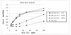
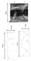
도 3은 예시적인 장치 및 비교 장치에 대한 이동성의 그래프이다.
도 4는 비교 장치의 유기 반도체 층의 원자력 현미경 이미지이다.
도 5는 예시적인 장치의 유기 반도체 층의 원자력 현미경 이미지이다.
도 6은 비교 장치의 단면의 두께 프로파일의 높이 프로파일을 도시한다.
도 7은 본 발명의 실시양태에 따른 예시적인 장치의 단면도의 두께 프로파일을 도시한다. The invention will now be described in more detail with reference to the drawings.
1 is a schematic diagram of a top gate transistor in accordance with an embodiment of the present invention.
2 is a schematic diagram of a bottom gate transistor in accordance with an embodiment of the present invention.
3 is a graph of mobility for an exemplary apparatus and a comparison apparatus.
4 is an atomic force microscope image of the organic semiconductor layer of the comparative device.
5 is an atomic force microscope image of an organic semiconductor layer of an exemplary device.
6 shows the height profile of the thickness profile of the cross section of the comparison device.
Figure 7 illustrates a thickness profile of a cross-sectional view of an exemplary device according to an embodiment of the present invention.
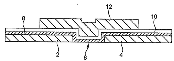
임의의 축척으로 도시되지 않은 도 1은 예시적인 상부 게이트 유기 박막 트랜지스터를 개략적으로 도시한다. 도시된 구조는 기판(나타내지 않음) 상에 증착될 수 있고 이들 사이에 위치된 채널 영역(6)과 이격된 소스 및 드레인 전극(2 및 4)을 포함한다. 채널 영역(6) 중 유기 반도체 층(8)은 소스 및 드레인 전극(2 및 4)과 접촉하고 소스 및 드레인 전극(2 및 4)의 적어도 일부에 걸쳐 확장될 수 있다. 유전체 물질의 절연층(10)은 유기 반도체 층(8)에 걸쳐 증착되고 소스 및 드레인 전극(2 및 4)의 적어도 일부에 걸쳐 확장될 수 있다. 최종적으로, 게이트 전극(12)은 절연층(10) 상에 증착된다. 게이트 전극(12)은 채널 영역(6)에 걸쳐 위치되고 소스 및 드레인 전극(2 및 4)의 적어도 일부에 걸쳐 확장될 수 있다.1, which is not shown in any scale, schematically illustrates an exemplary top gate organic thin film transistor. The illustrated structure includes source and
상기 기재된 구조는 게이트가 기판에 비해 장치의 상면에 위치됨으로써 상부 게이트 유기 박막 트랜지스터로서 공지된다. 다르게는, 또한 장치의 하면 상에 게이트를 제공하여 이른바 하부 게이트 유기 박막 트랜지스터를 형성하는 것이 공지된다.The structure described above is known as an upper gate organic thin film transistor by placing the gate on the upper surface of the device as compared to the substrate. Alternatively, it is also known to provide a gate on the underside of the device to form a so-called bottom gate organic thin film transistor.
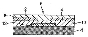
하부 게이트 유기 박막 트랜지스터의 예는 임의의 축척으로 도시되지 않은 도 2에 제시되어 있다. 도 1 및 2에 도시된 구조 사이의 관계를 더욱 분명하게 나타내기 위해, 예컨대 참조 번호가 상응하는 부분에 대하여 사용되었다. 도 2에 도시된 하부 게이트 구조는 이에 증착된 유전체 물질의 절연층(10)을 갖는 기판(1) 상에 증착된 게이트 전극(12)을 포함한다. 소스 및 드레인 전극(2 및 4)은 유전체 물질의 절연층(10) 상에 증착된다. 소스 및 드레인 전극(2 및 4)은 게이트 전극에 걸쳐 이 이 사이에 위치된 채널 영역(6)과 이격된다. 채널 영역(6) 중 유기 반도체 층(8)은 소스 및 드레인 전극(2 및 4)과 접촉하고 소스 및 드레인 전극(2 및 4)의 적어도 일부에 걸쳐 확장될 수 있다.An example of a bottom gate organic thin film transistor is shown in Figure 2, which is not shown in any scale. In order to more clearly illustrate the relationship between the structures shown in Figures 1 and 2, for example, reference numerals have been used for the corresponding parts. The bottom gate structure shown in FIG. 2 includes a
소분자Small molecule 유기 반도체 Organic semiconductor
예시적인 소분자 유기 반도체는 적어도 3개의 융합된 고리의 코어를 갖는 화합물을 포함하고, 이때 각각의 고리는 독립적으로 각각 개별적으로 비치환되거나 하나 이상의 치환기로 치환된 방향족 고리 및 헤테로방향족 고리로부터 선택된다. 바람직하게는, 코어는 적어도 하나의 치환기, 임의적으로 하나 이상의 가용화 치환기로 치환된다. An exemplary small molecule organic semiconductor comprises a compound having at least three fused ring cores wherein each ring is independently selected from an aromatic ring and a heteroaromatic ring, each of which is either unsubstituted or substituted with one or more substituents. Preferably, the core is substituted with at least one substituent, optionally at least one solubilizing substituent.
가용화 치환기는 비치환된 유기 반도체와 비교하여 유기 용매, 예를 들어 무극성 유기 용매 중 유기 반도체의 가용성을 증가시키는 치환기일 수 있다.The solubilising substituent may be a substituent that increases the solubility of the organic semiconductor in an organic solvent, such as a non-polar organic solvent, as compared to an unsubstituted organic semiconductor.
예시적인 치환기는 화학식 I 내지 V를 참조하여 기재된 치환기 X, 예를 들어 하나 이상의 알킬 기, 알콕시 기 또는 실릴 기, 예컨대 트라이알킬실릴 및 트라이알킬실릴에틴일을 포함한다. Exemplary substituents include the substituents X described with reference to Formulas I through V, such as one or more alkyl groups, alkoxy groups or silyl groups such as trialkylsilyl and trialkylsilylethynyl.
소분자 유기 반도체는 전자-풍부 화합물, 예를 들어 융합된 티오펜 반복 단위를 포함하는 화합물일 수 있다. The small molecule organic semiconductor may be an electron-rich compound, for example, a compound comprising a fused thiophene repeat unit.
예시적인 소분자 유기 반도체는 화학식 I 내지 V의 화합물을 포함한다.Exemplary small molecule organic semiconductors include compounds of Formulas I-V.
소분자 유기 반도체는 하기 화학식 VI, VII, VIII, IX 및 X의 화합물로부터 선택될 수 있다:The small molecule organic semiconductors may be selected from compounds of the formulas VI, VII, VIII, IX and X:
[화학식 VI](VI)

[상기 식에서,[In the above formula,
X1 및 X2는 동일하거나 상이할 수 있고, 화학식 I 내지 V를 참고하여 상기 기재된 바와 같은 치환기 X로부터 선택되고; X 1 and X 2 may be the same or different and are selected from Substituent X as described above with reference to Formulas I to V;
Z1 및 Z2는 독립적으로 S, O, Se 또는 NR4이고; Z 1 and Z 2 are independently S, O, Se or NR 4 ;
W1 및 W2는 독립적으로 S, O, Se, NR4 또는 -CR4=CR4-이고, 이때 R4는 H 또는 1 내지 20개의 탄소 원자를 갖는 치환된 또는 비치환된 선형, 분지형 또는 환형 알킬 기, 1 내지 12개의 탄소 원자를 갖는 알콕시 기, 비치환되거나 1 내지 8개의 탄소 원자를 갖는 1 또는 각각 동일하거나 상이할 수 있는 2개의 알킬 기로 치환될 수 있는 아미노 기, 아미도 기, 실릴 기 및 2 내지 12개의 탄소 원자를 갖는 알켄일 기로 이루어진 군으로부터 선택된 치환기이다]W 1 and W 2 are independently S, O, Se, NR 4, or -CR 4 = CR 4 -, and wherein R 4 is a substituted or unsubstituted linear, branched, having 1 to 20 carbon atoms or H Or an alkoxy group having 1 to 12 carbon atoms, an amino group which may be unsubstituted or substituted with one or two alkyl groups which may be the same or different from each other and which has 1 to 8 carbon atoms, , A silyl group and an alkenyl group having 2 to 12 carbon atoms]
[화학식 VII](VII)

[상기 식에서,[In the above formula,
X1 및 X2는 상기 화학식 VI을 참고하여 기재된 바와 같고;X 1 and X 2 are as described with reference to Formula VI above;
Z1, Z2, W1 및 W2는 상기 화학식 VI을 참고하여 기재된 바와 같고;Z 1 , Z 2 , W 1 and W 2 are as described above with reference to Formula VI;
V1 및 V2는 독립적으로 S, O, Se 또는 NR5이고, 이때 R5는 H 또는 1 내지 20개의 탄소 원자를 갖는 치환된 또는 비치환된 선형, 분지형 또는 환형 알킬 기, 1 내지 12개의 탄소 원자를 갖는 알콕시 기, 비치환되거나 1 내지 8개의 탄소 원자를 갖는 1 또는 각각이 동일하거나 상이할 수 있는 2개의 알킬 기로 치환될 수 있는 아미노 기, 아미도 기, 실릴 기 및 2 내지 12개의 탄소 원자를 갖는 알켄일 기로 이루어진 군으로부터 선택된 치환기이다]V 1 and V 2 are independently S, O, Se or NR 5 wherein R 5 is H or a substituted or unsubstituted linear, branched or cyclic alkyl group having 1 to 20 carbon atoms, An amino group, an amido group, a silyl group, and an alkyl group having 2 to 12 carbon atoms, which may be substituted with one or two alkyl groups, which may be the same or different, each having 1 to 8 carbon atoms, Lt; / RTI > carbon atoms,
[화학식 VIII](VIII)

[상기 식에서,[In the above formula,
X1 및 X2, Z1, Z2, W1 및 W2는 상기 화학식 VI을 참고하여 기재된 바와 같다]X 1 and X 2 , Z 1 , Z 2 , W 1 and W 2 are as described above with reference to the formula (VI)
[화학식 IX](IX)

[상기 식에서,[In the above formula,
Z1, Z2, W1 및 W2는 상기 화학식 VI을 참고하여 기재된 바와 같고;Z 1 , Z 2 , W 1 and W 2 are as described above with reference to Formula VI;
동일하거나 상이할 수 있는 X1 내지 X10은 화학식 I 내지 V를 참고하여 기재된 바와 같은 치환기 X로부터 선택된다]X 1 to X 10, which may be the same or different, are selected from Substituent X as described with reference to Formulas I to V,
[화학식 X](X)

[상기 식에서,[In the above formula,
A는 페닐 기 또는 티오펜 기이고, 상기 페닐 기 또는 티오펜 기는 임의적으로 페닐 기, 티오펜 기 및 벤조티오펜 기로부터 선택된 기와 임의적으로 융합될 수 있는 페닐 기 또는 티오펜 기와 융합되고, 임의의 상기 페닐, 티오펜 및 벤조티오펜 기는 비치환되거나 X11의 적어도 하나의 기로 치환되고;A is a phenyl group or a thiophene group, the phenyl or thiophene group is optionally fused with a phenyl or thiophene group optionally fused to a group selected from a phenyl group, a thiophene group and a benzothiophene group, The phenyl, thiophene and benzothiophene groups are unsubstituted or substituted with at least one group of X < 11 & gt ;;
각각의 기 X11은 동일하거나 상이할 수 있고 화학식 I 내지 V를 참고하여 기재된 바와 같은 치환기 X로부터 선택되고, 바람직하게는 화학식 CnH2n +1의 기이고, 이때 n은 1 내지 20의 정수이다].Each group X < 11 > may be the same or different and is selected from a substituent X as described with reference to Formulas I to V, preferably a group of the formula C n H 2n +1 , where n is an integer from 1 to 20 to be].
화학식 X의 화합물에서, A는 임의적으로 하기로부터 선택된다:In compounds of formula X, A is optionally selected from:
화학식 X11의 적어도 하나의 기로 치환된 페닐 기로 융합된 티오펜 기; 및A thiophene group fused to a phenyl group substituted with at least one group of the formula X 11 ; And
비치환되거나 화학식 X11의 적어도 하나의 기로 치환될 수 있는 페닐 기이고, 또한 임의적으로 비치환되거나 화학식 X11의 적어도 하나의 기로 치환될 수 있는 티오펜 기와 융합되고/되거나 벤조티오펜 기와 융합되고, 상기 벤조티오펜 기는 비치환되거나 화학식 X11의 적어도 하나의 기로 치환되고, 이때 X11이 화학식 CnH2n +1의 기이고, 이때 n이 1 내지 16의 정수인, 페닐 기.Phenyl which is unsubstituted or may be substituted with at least one of the formula X 11 group, also optionally unsubstituted or is fused thiophene group which may be substituted with at least one of the formula X 11 / or benzothiophene group is fused , the benzothiophene group is unsubstituted or is substituted with at least one of the formula X 11, wherein X 11 is a group of the formula C n H 2n +1, wherein n is an integer of from 1 to 16, a phenyl group.
화학식 X의 화합물은 하기 화합물을 포함한다:The compounds of formula X include the following compounds:


상기 식에서,In this formula,
X11은 화학식 CnH2n +1 의 기이고, 이때 n은 1 내지 16의 정수이다.X 11 is a group of the formula C n H 2n + 1, where n is an integer from 1 to 16;
화학식 III의 바람직한 화합물은 하나 이상의 트라이(C1-10 알킬)실릴에틴일 기로 치환된 펜타센이다. 바람직하게는, 트라이(C1-10 알킬)실릴에틴일 치환기가 펜타센의 6-위치 및 13-위치에서 제공된다. 예시적인 치환된 펜타센은 하기 6,13-(트라이-이소프로필-실릴에틴일) 펜타센(TIPS 펜타센)이다:A preferred compound of formula III is pentacene substituted with one or more tri (C 1-10 alkyl) silylethynyl groups. Preferably, tri (C 1-10 alkyl) silylethynyl substituents are provided at the 6-position and 13-position of the pentacene. An exemplary substituted pentacene is 6,13- (tri-isopropyl-silylethynyl) pentacene (TIPS pentacene)

TIPS 펜타센TIPS pentacene
소분자 유기 반도체의 하나 이상의 치환기, 예를 들어 상기 기재된 바와 같은 치환기 X 및 X1 내지 X11은 (a) 유기 반도체 코어의 말단에서 일환형 방향족 또는 헤테로방향족 고리 중 하나 또는 둘다에서; (b) 유기 반도체 코어의 말단에서가 아닌 일환형 방향족 또는 헤테로방향족 고리 중 하나 이상에서; 또는 상기 (a) 및 (b) 둘다에서 제공될 수 있다.One or more substituents of the small molecule organic semiconductor, for example substituents X and X 1 to X 11 as described above, may be selected from (a) at one or both of the monocyclic aromatic or heteroaromatic rings at the end of the organic semiconductor core; (b) at least one of the monocyclic aromatic or heteroaromatic rings not at the end of the organic semiconductor core; Or in both (a) and (b) above.
소분자Small molecule 결정화 crystallization 개질제Modifier
소분자 결정화 개질제는 결정화 개질제가 존재하지 않는 장치와 비교하여 유기 반도체 층에서 소분자 유기 반도체 분포의 균일성을 증가시킬 수 있다. 결정화 개질제가 없는 조성물이 상이한 표면적을 갖는 표면 상에서 증착되는 경우, 소분자 유기 반도체의 결정화는 결정화가 거의 없거나 전혀 없는 하나 이상의 다른 면적의 이격이 발생하여 이러한 면적 중 하나 또는 일부에서 농축되고 높고 낮은 소분자 유기 반도체 농도의 면적을 갖는 막을 야기할 수 있다. 상이한 표면적 사이의 차이는 표면 물질의 차이, 표면 처리의 차이 및 표면 에너지의 차이 중 하나 이상일 수 있다.The small molecule crystallization modifier can increase the uniformity of the distribution of small molecule organic semiconductors in the organic semiconductor layer as compared to a device in which no crystallization modifier is present. When a composition without a crystallization modifier is deposited on a surface having a different surface area, the crystallization of the small molecule organic semiconductor results in separation of one or more other areas with little or no crystallization and is concentrated in one or more of these areas, A film having an area of semiconductor concentration can be caused. The difference between the different surface areas may be at least one of differences in surface material, difference in surface treatment and difference in surface energy.
소스 및 드레인 전극 및 채널 상에 조성물을 증착하는 경우(소스 및 드레인 전극 및/또는 채널은 표면 개질 처리를 시행할 수 있거나 시행할 수 없음), 결정화 개질제는 소분자 유기 반도체의 결정화를 야기하여 소분자 유기 반도체 결정이 실질적으로 소스와 드레인 전극 사이, 바람직하게는 소스 및 드레인 전극에 걸쳐 채널의 전체 길이를 가로질러 확장하는 유기 반도체 층을 생성할 수 있다. When the composition is deposited on the source and drain electrodes and channel (source and drain electrodes and / or channels can or may not be subjected to surface modification treatment), the crystallization modifier causes crystallization of the small molecule organic semiconductor, It is possible to produce an organic semiconductor layer in which crystals extend substantially across the entire length of the channel between the source and drain electrodes, preferably across the source and drain electrodes.
결정화 개질제가 없는 경우, 소분자 유기 반도체는 소분자 유기 반도체 결정이 실질적으로 채널의 전제 길이를 가로질러 확장하지 않은 불균일 두께의 유기 반도체 막을 야기하여 수직 방향으로 결정화될 수 있다. 결정화 개질제는 유기 반도체 층 막 두께의 균일성을 증가시킬 수 있다.In the absence of a crystallization modifier, the small molecule organic semiconductor can crystallize in a vertical direction by causing an organic semiconductor film of non-uniform thickness that does not extend substantially across the entire length of the channel. The crystallization modifier can increase the uniformity of the film thickness of the organic semiconductor layer.
결정화 개질제는 결정화 개질제가 없는 조성물을 증착함으로써 형성된 유기 반도체 막과 비교하여, 결정질 소분자 유기 반도체 물질이 채널 영역 내의 측면으로 추가로 확장되고 결과적으로 채널 내에 임의적으로 소스 및 드레인 전극에 걸쳐 더욱 균일하게 분포될 수 있는 효과와 함께, 하나 또는 적은 수의 핵 생성 위치상에 중심된 거대 결정 성장의 에너제틱한 유리성을 감소시킬 수 있다. 이는 결정 성장이 억제되지 않은 장치와 비교하여, 채널 내에 상이한 면적을 가로지르는 더 좁은 분포의 이동성을 갖는 채널을 제공할 수 있다.The crystallization modifier is further improved in that the crystalline small molecule organic semiconductor material is further extended to the side in the channel region and consequently more uniformly distributed in the channel over the source and drain electrodes as compared to the organic semiconductor film formed by depositing the composition without the crystallization modifier It is possible to reduce the energetic vitality of the centralized crystal growth on one or a few nucleation sites. This can provide a channel with a narrower distribution of mobility across the different areas in the channel compared to devices where crystal growth is not inhibited.
상기 기재된 소분자 유기 반도체, 예를 들어 본 발명의 조성물, 및 생성된 장치의 결정화 개질제가 제공된 임의의 화학식 I 내지 X에 따른 소분자 유기 반도체로부터 선택될 수 있는 소분자 결정화 개질제는, 구조적으로 유기 반도체와 상이하다. The small molecule crystallization modifiers that can be selected from the small molecule organic semiconductors described above, such as the compositions of the present invention, and the small molecule organic semiconductors according to any of formulas I to X provided with crystallization modifiers of the resulting apparatus, Do.
소분자 결정화 개질제는 소분자 유기 반도체와 동일한 코어를 가질 수 있지만 적어도 하나의 상이한 치환기를 가질 수 있다. 예를 들어, 결정화 개질제 및 유기 반도체는 화학식 I 내지 X의 코어로부터 선택된 동일한 코어를 가질 수 있지만 상이한 치환기를 가질 수 있다. 치환기의 차이는 치환기 X 및 X1 내지 X11 중 하나 이상의 차이; 치환 위치의 차이; 및 치환기 수의 차이 중 하나 이상일 수 있다. 바람직한 배열에서, 치환기는 상이하다. 예를 들어, 소분자 유기 반도체는 C1-20 알킬 기를 갖는 하나 이상의 위치에서 치환된 코어를 가질 수 있고, 소분자 결정화 개질제는 동일한 위치 또는 위치들에서 치환된 동일한 코어를 가질 수 있지만, 결정화 개질제 중 적어도 하나의 치환기는 유기 반도체의 상응하는 위치에서 C1-20 알킬 기와 상이한 C1 -20 알킬 기이다.The small molecule crystallization modifier may have the same core as the small molecule organic semiconductor, but may have at least one different substituent. For example, the crystallization modifier and the organic semiconductor may have the same core selected from the core of formulas I to X, but may have different substituents. The difference in substituents may be a difference of at least one of substituent X and X 1 to X 11 ; Difference in substitution position; And the difference in the number of substituents. In a preferred arrangement, the substituents are different. For example, the small molecule organic semiconductor may have a core substituted at one or more positions with a C 1-20 alkyl group, and the small molecule crystallization modifier may have the same core substituted at the same position or positions, but at least one of the crystallization modifiers one of the substituents is in the position corresponding to C 1-20 alkyl group and different C 1 -20 alkyl group of the organic semiconductor.
소분자 결정화 개질제는 동일한 치환기지만 소분자 유기 반도체에 상이한 코어를 가질 수 있다. 이 경우, 유기 반도체 및 결정화 개질제는 화학식 I 내지 X의 화합물일 수 있다.Small molecule crystallization modifiers are the same substituents but may have different cores in small molecule organic semiconductors. In this case, the organic semiconductor and the crystallization modifying agent may be the compounds of the formulas (I) to (X).
소분자 결정화 개질제 및 소분자 유기 반도체는 상이한 코어 및 상이한 치환기를 가질 수 있다. 이 경우, 유기 반도체 및 결정화 개질제는 각각 화학식 I 내지 X의 화합물로부터 선택될 수 있고, 유기 반도체 및 결정화 개질제의 코어 및 치환기는 둘다 상이하다.Small molecule crystallization modifiers and small molecule organic semiconductors may have different cores and different substituents. In this case, the organic semiconductor and the crystallization modifying agent may be selected from the compounds of the formulas (I) to (X), respectively, and the core and the substituent of the organic semiconductor and the crystallization modifying agent are both different.
바람직한 실시양태에서, 소분자 유기 반도체 및 소분자 결정화 개질제는 둘다 화학식 X의 화합물이고, 둘다 하기 화학식을 갖는 화합물일 수 있고, 이때 적어도 하나의 치환기 X11 및/또는 X11 치환 위치는 유기 반도체와 결정화 개질제 사이에서 상이하다:In a preferred embodiment, the small molecule organic semiconductor and the small molecule crystallization modifier are both compounds of formula X, both of which may be compounds having the formula: wherein at least one substituent X 11 and / or X 11 substitution position is an organic semiconductor and a crystallization modifier Lt; / RTI >

상기 식에서,In this formula,
X11은 화학식 CnH2n +1의 기이고, 이때 n은 1 내지 16의 정수이다.X 11 is a group of the formula C n H 2n + 1, where n is an integer from 1 to 16;
소분자 유기 반도체:소분자 결정화 개질제의 중량비는 임의적으로 적어도 2:1, 임의적으로 적어도 5:1, 임의적으로 적어도 10:1 및 임의적으로 적어도 20:1이다.The weight ratio of small molecule organic semiconductor: small molecule crystallization modifier is optionally at least 2: 1, optionally at least 5: 1, optionally at least 10: 1 and optionally at least 20: 1.
조성물은 본질적으로 소분자로 이루어질 수 있고, 본질적으로 소분자 유기 반도체 및 소분자 결정화 개질제로 이루어질 수 있다. 다른 배열에서, 하나 이상의 중합체는 조성물에 존재할 수 있다.The composition may consist essentially of small molecules and may consist essentially of small molecule organic semiconductors and small molecule crystallization modifiers. In other arrangements, one or more polymers may be present in the composition.
중합체polymer
존재하는 경우 중합체는 비전도성 및 반도체성 중합체를 포함하는 임의의 가용성 중합체일 수 있다.The polymer, if present, can be any soluble polymer, including nonconductive and semiconducting polymers.
예시적인 비전도성 중합체는 폴리스티렌 및 폴리아크릴레이트, 예를 들어 PMMA를 포함한다.Exemplary nonconductive polymers include polystyrene and polyacrylates, such as PMMA.
바람직한 반도체성 중합체는 서로에게 공액 결합된 반복 단위를 포함하는 중합체 골격을 갖는다.Preferred semiconducting polymers have a polymer backbone comprising repeating units conjugated to each other.
공액결합된 중합체의 예시적인 반복 단위는 (헤테로)아릴렌 반복 단위, (헤테로)아릴렌비닐렌 반복 단위 및 (헤테로)아릴아민 반복 단위를 포함한다.Exemplary repeat units of the conjugated polymer include (hetero) arylene repeat units, (hetero) arylene vinylene repeat units and (hetero) arylamine repeat units.
예시적인 (헤테로)아릴아민 반복 단위는 하기 화학식 XI의 반복 단위를 포함한다:Exemplary (hetero) arylamine repeat units include repeat units of formula (XI)
[화학식 XI](XI)

상기 식에서,In this formula,
각각의 경우 Ar1 및 Ar2는 독립적으로 치환된 또는 비치환된 아릴 또는 헤테로아릴 기로부터 선택되고; In each case Ar 1 and Ar 2 are independently selected from substituted or unsubstituted aryl or heteroaryl groups;
n은 1 이상, 바람직하게는 1 또는 2이고; n is 1 or more, preferably 1 or 2;
각각의 경우 R은 H 또는 치환기, 바람직하게는 치환기이고; In each case R is H or a substituent, preferably a substituent;
x 및 y는 각각 독립적으로 1, 2 또는 3이다. x and y are each independently 1, 2 or 3;
예시적인 기 R은 알킬 및 아릴, 예를 들어 페닐을 포함한다. Exemplary groups include alkyl and aryl, such as phenyl.
R이 아릴인 경우, 임의의 Ar1, Ar2 및 R은 독립적으로 하나 이상의 치환기로 치환될 수 있다. 바람직한 치환기는 하기로 이루어진 기 R3으로부터 선택된다:When R is aryl, any of Ar 1, Ar 2 and R may be substituted with one or more substituents independently. Preferred substituents are selected from the group R < 3 >
하나 이상의 비인접한 C 원자가 O, S, 치환된 N, C=O 및 -COO-로 대체될 수 있고 알킬 기의 하나 이상의 H 원자가 F, 또는 하나 이상의 기 R6으로 치환된 또는 비치환된 아릴 또는 헤테로아릴로 대체될 수 있는, 알킬;One or more non-adjacent C atom is O, S, substituted by N, C = O, and could be replaced by -COO-, and the alkyl groups one or more H atoms are F, or at least one group R 6 represent a substituted or unsubstituted aryl group or a Alkyl, which may be substituted by heteroaryl;
하나 이상의 기 R6으로 치환된 또는 비치환된 아릴 또는 헤테로아릴;Aryl or heteroaryl substituted with one or more groups R < 6 & gt ;;
NR5 2, OR5, SR5; 및NR 5 2 , OR 5 , SR 5 ; And
불소, 니트로 및 시아노Fluorine, nitro, and cyano
[이때, 각각의 R6은 독립적으로 하나 이상의 비인접한 C 원자가 O, S, 치환된 N, C=O 및 -COO-로 대체될 수 있고 알킬 기의 하나 이상의 H 원자는 F로 대체될 수 있는 알킬이고, 각각의 R5는 독립적으로 알킬 및 하나 이상의 알킬 기로 치환된 또는 비치환된 아킬 및 아릴 또는 헤테로아릴로 이루어진 군으로부터 선택된다].Wherein each R < 6 > independently can be substituted with one or more non-adjacent C atoms O, S, substituted N, C = O, and -COO-, and one or more H atoms of the alkyl group may be replaced by F Alkyl, each R < 5 > is independently selected from the group consisting of alkyl and substituted or unsubstituted aryl and heteroaryl with one or more alkyl groups.
바람직하게는, x, y 및 n은 모두 1이다.Preferably, x, y and n are all 1s.
바람직하게는, Ar1, Ar2 및 R은 각각 페닐이고 각각 독립적으로 하나 이상의 C1-20 알킬 기로 치환된 또는 비치환된 페닐이다. 바람직한 배열에서, Ar1 및 Ar2는 비치환된 페닐이고 R은 C1 -20 알킬 기로 치환된 페닐이다.Preferably, Ar < 1 >, Ar < 2 > and R < 2 > are each phenyl and each independently phenyl substituted with one or more C1-20 alkyl groups or unsubstituted phenyl. In a desired arrangement, Ar 1 and Ar 2 are unsubstituted phenyl and R is a substituted phenyl group C 1 -20 alkyl.
예시적인 아릴렌 반복 단위는 페닐렌, 플루오렌 및 인데노플루오렌 반복 단위를 포함하고, 이들 각각은 하나 이상의 치환기로 치환될 수 있다.Exemplary arylene repeat units include phenylene, fluorene, and indenofluorene repeat units, each of which may be substituted with one or more substituents.
예시적인 플루오렌 반복 단위는 화학식 XII의 반복 단위를 포함한다:Exemplary fluorene repeat units include repeat units of formula XII:
[화학식 XII](XII)

상기 식에서,In this formula,
동일하거나 상이할 수 있는 2개의 기 R7은 각각 H 또는 치환기이고, 2개의 기 R7은 연결되어 고리를 형성할 수 있다. The two groups R 7, which may be the same or different, are each H or a substituent, and the two groups R 7 may be connected to form a ring.
각각의 R7은 임의적으로 수소; 치환된 또는 비치환된 아릴 또는 헤테로아릴, 바람직하게는 치환된 또는 비치환된 페닐; 및 치환된 또는 비치환된 알킬로 이루어진 군으로부터 선택되고, 이때 알킬 기의 하나 이상의 비인접한 C 원자는 O, S, 치환된 N, C=O 및 -COO-로 대체될 수 있다.Each R < 7 > is optionally hydrogen; Substituted or unsubstituted aryl or heteroaryl, preferably substituted or unsubstituted phenyl; And substituted or unsubstituted alkyl, wherein at least one non-adjacent C atom of the alkyl group may be replaced by O, S, substituted N, C = O, and -COO-.
R7이 알킬을 포함하는 경우, 알킬 기의 임의의 치환기는 F, 시아노, 니트로, 및 하나 이상의 기 R6으로 치환된 또는 비치환된 아릴 또는 헤테로아릴을 포함하고, 이때 R6은 상기 기재된 바와 같다.When R 7 comprises alkyl, any substituent of the alkyl group includes F, cyano, nitro, and substituted or unsubstituted aryl or heteroaryl with one or more groups R 6 , wherein R 6 is as defined above Same as.
R7이 아릴 또는 헤테로아릴을 포함하는 경우, 각각의 아릴 또는 헤테로아릴 기는 독립적으로 치환될 수 있다. 아릴 또는 헤테로아릴 기에 대한 바람직한 임의의 치환기는 C1 -20 알킬을 포함한다.When R 7 comprises aryl or heteroaryl, each aryl or heteroaryl group may be independently substituted. Preferred optional substituents for the aryl or heteroaryl groups include C 1 -20 alkyl.
치환기 R7을 제외하고 플루오렌 단위에 대한 임의의 치환기는 바람직하게는 하나 이상의 비인접한 C 원자가 O, S, 치환된 N, C=O 및 -COO-로 대체될 수 있는 알킬; 치환된 또는 비치환된 아릴, 예를 들어 하나 이상의 알킬 기로 치환된 또는 비치환된 페닐; 치환된 또는 비치환된 헤테로아릴; 불소, 시아노 및 니트로로 이루어진 군으로부터 선택된다.Except for the substituent R 7 , any substituent for the fluorene unit is preferably alkyl in which one or more non-adjacent C atoms can be replaced by O, S, substituted N, C = O, and -COO-; Substituted or unsubstituted aryl, e.g., phenyl substituted with one or more alkyl groups; Substituted or unsubstituted heteroaryl; Lt; / RTI > is selected from the group consisting of fluorine, cyano, and nitro.
존재하는 경우, 화학식 XII의 반복 단위 중 치환된 N은 각각의 경우 독립적으로 화학식 XI을 참고하여 기재된 바와 같은 NR5일 수 있다.When present, the substituted N in the repeating unit of formula (XII) can in each case independently be NR < 5 >, as described with reference to formula (XI).
하나의 바람직한 배열에서, 하나 또는 두가지 경우에 R7은 치환된 또는 비치환된 C1-C20 알킬 또는 치환된 또는 비치환된 아릴 기, 특히 하나 이상의 C1 -20 알킬 기로 치환된 페닐로부터 선택된다.In one preferred arrangement, in one or both cases, R 7 is selected from substituted or unsubstituted C 1 -C 20 alkyl or substituted or unsubstituted aryl groups, especially phenyl substituted with one or more C 1 -20 alkyl groups do.
하나의 바람직한 실시양태에서, 중합체는 화학식 XI의 반복 단위 및 화학식 XII의 반복 단위의 1:1 공중합체이다.In one preferred embodiment, the polymer is a 1: 1 copolymer of a repeating unit of formula (XI) and a repeating unit of formula (XII).
용매menstruum
소분자 유기 반도체, 소분자 결정화 개질제 및 (존재하는 경우) 중합체의 용해를 위한 예시적인 용매는 벤젠 또는 융합된 벤젠을 포함하고, 이들 각각은 하나 이상의 치환기로 치환될 수 있다. 융합된 벤젠은 벤젠에 융합된 포화된 고리 및 불포화된 고리를 갖는 화합물, 예를 들어 테트랄린(1,2,3,4-테트라하이드로나프탈렌) 및 인단(2,3-다이하이드로인덴)을 포함한다.Exemplary solvents for the dissolution of small molecule organic semiconductors, small molecule crystallization modifiers and, if present, polymers include benzene or fused benzene, each of which may be substituted with one or more substituents. The fused benzene may be a compound having a saturated ring and an unsaturated ring fused to benzene, such as tetralin (1,2,3,4-tetrahydronaphthalene) and indane (2,3-dihydroindene) .
벤젠 또는 융합된 벤젠에 대한 하나 이상의 치환기는 알킬 및 알콕시 치환기의 기, 임의적으로 C1 -10 알킬 및 C1 -10 알콕시 치환기, 바람직하게는 C1 -5 알킬 및 C1 -5 알콕시로부터 선택될 수 있다. 예시적인 용매는 자일렌, 하나 이상의 C1 -5 알킬 기로 치환된 아니솔, 메틸나프탈렌 및 메톡시나프탈렌을 포함한다.Benzene or fused benzene is selected from a group of alkyl and alkoxy substituents, optionally a C 1 -10 alkyl and a C 1 -10 alkoxy substituent, preferably C 1 -5 alkyl and C 1 -5 alkoxy . Exemplary solvents include xylene, at least one C 1 -5 alkyl substituted with the anisole, naphthalene, and methyl-methoxynaphthalene.
용매는 60 내지 240 ℃의 범위에서 비점을 가질 수 있다. 본 발명의 조성물 중 소분자 결정화 개질제의 존재로부터 야기하는 유기 반도체 층 막의 개질된 균일성은 용매를 빠르게 증발시킬 필요가 없음을 의미한다. 따라서, 조성물은 적어도 100 ℃의 비점을 갖는 용매를 포함할 수 있다. The solvent may have a boiling point in the range of 60 to 240 캜. The modified homogeneity of the organic semiconductor layer film resulting from the presence of the small molecule crystallization modifier in the composition of the present invention means that it is not necessary to rapidly evaporate the solvent. Thus, the composition may comprise a solvent having a boiling point of at least 100 < 0 > C.
용액 가공Solution processing
유기 반도체 막을 형성하기 위해 본 발명의 조성물을 증착하기 위한 적합한 방법은 코팅 방법(즉, 전체 표면이 무분별하게 코팅됨) 및 프린팅 가공(즉, 조성물이 표면의 전체가 아니 일부에 선택적으로 증착됨)을 포함한다.Suitable methods for depositing the compositions of the present invention to form the organic semiconductor film include coating methods (i.e., the entire surface is indiscriminately coated) and the printing process (i.e., the composition is selectively deposited on a portion, .
예시적인 코팅 가공은 스핀 코팅, 침지 코팅, 슬롯 다이 코팅 및 닥터 블레이드 코팅을 포함한다.Exemplary coating processes include spin coating, dip coating, slot die coating, and doctor blade coating.
예시적인 프린팅 가공은 잉크젯 프린팅, 플랙소그래픽 프린팅 및 그라비어 프린팅을 포함한다.Exemplary printing processes include inkjet printing, flexographic printing and gravure printing.
증착 후, 용매는 주변 조건에서 증발하도록 허용될 수 있다. 다르게는, 용매는 고온, 예를 들어 50 ℃ 이상 및/또는 감압에서 증발될 수 있다.After deposition, the solvent may be allowed to evaporate under ambient conditions. Alternatively, the solvent may be evaporated at elevated temperatures, such as at least 50 < 0 > C and / or reduced pressure.
소스, sauce, 드레인drain 및 게이트 전극 And the gate electrode
소스, 드레인 및 게이트 전극은 광범위한 전도성 물질, 예를 들어 금속(예컨대, 금), 금속 합금, 금속 화합물(예컨대, 인듐 주석 옥사이드) 또는 전도성 중합체로부터 선택될 수 있다. The source, drain and gate electrodes may be selected from a wide variety of conductive materials, such as metal (e.g., gold), metal alloys, metal compounds (such as indium tin oxide), or conductive polymers.
게이트 전극, 소스 및 드레인 전극의 두께는 원자력 현미경(AFM)에 의해 측정된 바, 5 내지 200 mm의 영역일 수 있다. The thickness of the gate electrode, source and drain electrodes may be in the region of 5 to 200 mm as measured by an atomic force microscope (AFM).
게이트 gate 절연층Insulating layer
게이트 절연층은 높은 저항률을 갖는 절연 물질로부터 선택된 유전체 물질을 포함한다. 게이트 유전체의 유전체 상수(k)는 비록 높은 값의 k를 갖는 물질이 바람직할지라도 OTFT를 달성할 수 있는 정전 용량이 k에 정비례하기 때문에 전형적으로 약 2 내지 3이고, 드레인 전류는 정전 용량에 정비례한다. 따라서, 낮은 운전 전압을 갖는 높은 드레인 전류를 달성하기 위해, 채널 영역 내에 박 유전체 층을 갖는 OTFT가 바람직하다. 절연층의 두께는 바람직하게는 2 ㎛ 미만, 더욱 바람직하게는 500 nm 미만이다. The gate insulating layer includes a dielectric material selected from an insulating material having a high resistivity. The dielectric constant k of the gate dielectric is typically about 2 to 3 because the capacitance that can attain OTFT is directly proportional to k, although a material with a high value of k may be desirable, and the drain current is proportional to capacitance do. Thus, to achieve a high drain current with a low operating voltage, an OTFT having a thin dielectric layer in the channel region is preferred. The thickness of the insulating layer is preferably less than 2 mu m, more preferably less than 500 nm.
게이트 유전체 물질은 유기 물질 또는 무기 물질일 수 있다. 바람직한 무기 물질은 SiO2, SixNy, 실리콘 옥시니트라이드 및 스핀-온-글라스(SOG)를 포함한다. 유기 유전체 물질은 플루오르화 중합체, 예컨대 폴리테트라플루오로에틸렌(PTFE), 퍼플루오로 사이클로 옥시지방족 중합체(CYTOP), 퍼플루오로알콕시 중합체 수지(PFA), 플루오르화 에틸렌-프로필렌(FEP), 폴리에틸렌테트라플루오로에틸렌(ETFE), 폴리비닐플루오라이드(PVF), 폴리에틸렌클로로트라이플루오로에틸렌(ECTFE), 폴리비니릴덴 플루오라이드(PVDF), 폴리클로로트라이플루오로에틸렌(PCTFE), 퍼플루오로 엘라스토머(FFKM), 예컨대 칼레즈(Kalrez)(RTM) 또는 테크노플론(Tecnoflon)(RTM), 플루오로 엘라스토머, 예컨대 비톤(Viton)(RTM), 퍼플루오로폴리에터(PFPE), 및 테트라플루오로에틸렌, 헥사플루오로프로필렌 및 비니릴덴 플루오라이드의 중합체(THV)를 포함한다.The gate dielectric material may be an organic material or an inorganic material. Preferred inorganic materials include SiO 2 , Si x N y , silicon oxynitride and spin-on-glass (SOG). The organic dielectric material may include fluorinated polymers such as polytetrafluoroethylene (PTFE), perfluorocyclooxy aliphatic polymers (CYTOP), perfluoroalkoxy polymer resins (PFA), fluorinated ethylene-propylene (FEP), polyethylene tetra (PCTFE), perfluoroelastomers (FFKM), polyvinyl fluoride (PVF), polyethylene terephthalate (EPTFE), polyvinylidene fluoride (PVDF), polychlorotrifluoroethylene Such as Kalrez (RTM) or Tecnoflon (RTM), fluoroelastomers such as Viton (RTM), perfluoropolyether (PFPE), and tetrafluoroethylene, Polymers of hexafluoropropylene and vinylidene fluoride (THV).
비플루오르화 유기 중합체 절연용 물질이 또한 사용될 수 있고 중합체, 예컨대 폴리 비닐알코올(PVA), 폴리비닐피롤리돈, 폴리비닐페놀, 아크릴레이트, 예컨대 다우 코닝(Dow Corning)으로부터 입수가능한 폴리메틸메타크릴레이트(PMMA) 및 벤조사이클로부탄(BCB)을 포함한다. 절연층은 물질의 배합으로부터 형성될 수 있다. 다층 구조는 단일 절연층 대신에 사용될 수 있다.Non-fluorinated organic polymer insulating materials can also be used and include polymers such as polyvinyl alcohol (PVA), polyvinyl pyrrolidone, polyvinyl phenol, acrylates such as polymethyl methacrylate available from Dow Corning (PMMA) and benzocyclobutane (BCB). The insulating layer may be formed from a combination of materials. The multi-layer structure can be used instead of a single insulating layer.
게이트 유전체 물질은 진공하에 열적 진공에 의해 또는 당해 분야에 공지된 적층 기술에 의해 증착될 수 있다. 다르게는, 유전체 물질은 예를 들어, 스핀 코팅 또는 잉크젯 프린팅 기술 및 상기 기재된 다른 용액 증착 기술을 사용하여 용액으로부터 증착될 수 있다. The gate dielectric material may be deposited by thermal vacuum under vacuum or by deposition techniques known in the art. Alternatively, the dielectric material can be deposited from solution using, for example, spin-coating or ink-jet printing techniques and other solution deposition techniques described above.
유전체 물질이 유기 반도체 층 위에 용액으로부터 증착되는 경우, 이는 유기 반도체 층의 용해를 야기하지 않아야 한다. 마찬가지로, 유전체 물질은 유기 반도체 층이 용액으로부터 이 위에 증착되는 경우, 용해되지 않아야 한다. 이러한 용해를 피하기 위한 기술은 직교 용매의 사용, 즉, 기저 층을 용해하지 않는 최상 층의 증착을 위한 용매의 사용; 및 기저 층의 가교를 포함한다. If a dielectric material is deposited from solution on the organic semiconductor layer, it should not cause dissolution of the organic semiconductor layer. Likewise, the dielectric material must not dissolve when the organic semiconductor layer is deposited thereon from solution. Techniques for avoiding such dissolution include the use of orthogonal solvents, i.e., the use of a solvent for the deposition of the top layer that does not dissolve the base layer; And crosslinking of the base layer.
추가 층Additional layer
예를 들어 접촉 저항을 감소하고 점착을 촉진하기 위해 다른 층이 장치 구조에 포함될 수 있다. For example, other layers may be included in the device structure to reduce contact resistance and promote adhesion.
채널 영역(즉, 소스와 드레인 전극 사이의 영역)의 표면은 결합 기 및 유기 기를 포함하는 물질을 포함하는 모노층으로 제공될 수 있다. 상기 모노층에 대한 예시적인 물질은 실란, 클로로- 또는 알콕시-실란, 예를 들어 C1 -20 알킬, 페닐 및 페닐-C1 - 20알킬로부터 선택된 하이드로카빌 기로 치환된 트라이클로로실란을 포함한다.The surface of the channel region (i. E., The region between the source and drain electrodes) may be provided with a mono layer comprising a material comprising a bonding group and an organic group. Exemplary materials for the mono-layer is a silane, dichloro-or alkoxy-silanes, such as C 1 -20 alkyl, phenyl, phenyl -C 1 - comprises a group selected from hydrocarbyl substituted 20 alkyl trimethyl chlorosilane.
소스 및 드레인 전극은 표면 개질 처리, 예를 들어 인터페이스 소스-드레인 전극/유기 반도체 층에서 접촉 저항을 줄이기 위해 이용될 수 있다. 표면 개질 처리는 소스 및 드레인 전극의 일함수의 변형을 야기할 수 있다.The source and drain electrodes may be used to reduce the contact resistance in the surface modification process, for example, the interface source-drain electrode / organic semiconductor layer. The surface modification treatment may cause deformation of the work function of the source and drain electrodes.
소스 및 드레인 전극은 유기 반도체 층과 접촉하는 소스 및 드레인 전극 표면의 적어도 일부를 덮는 표면-개질화 화합물로 제공될 수 있다. 표면-개질화 화합물은 유기 반도체와 전극 사이의 접촉 저항을 줄일 수 있다. 예시적인 표면-개질화 화합물은 비공액결합된 유기 기, 예를 들어 알킬 기, 및/또는 공액결합된 유기 기, 예를 들어 플루오르화 벤젠, 예컨대 펜타페닐벤젠, 및 유기 반도체를 도핑할 수 있는 유기 화합물을 가질 수 있다. 예시적인 도판트는 전하-중성 도판트, 예를 들어 치환된 또는 비치환된 테트라시아노퀴노다이메탄(TCNQ)을 포함한다. 예시적인 치환된 TCNQ는 테트라플루오로테트라시아노퀴노다이메탄(F4TCNQ)이다.The source and drain electrodes may be provided with a surface-reforming compound covering at least a portion of the surface of the source and drain electrodes in contact with the organic semiconductor layer. The surface-modified compound can reduce the contact resistance between the organic semiconductor and the electrode. Exemplary surface-modified compounds include those that can be doped with non-conjugated organic groups such as alkyl groups, and / or conjugated organic groups such as fluorinated benzenes such as pentaphenylbenzene, and organic semiconductors Organic compounds. Exemplary dopants include charge-neutral dopants, for example, substituted or unsubstituted tetracyanoquinodimethane (TCNQ). An exemplary substituted TCNQ is tetrafluorotetracyanoquinodiacetane (F4TCNQ).
전자 결핍 표면 개질화 화합물, 예를 들어 모노- 또는 폴리-플루오르화 방향족은 전자 풍부 유기 반도체, 예를 들어 하나 이상의 티오펜 고리를 포함하는 유기 반도체로 사용하기에 특히 적합할 수 있다.Electron-deficient surface modifying compounds, such as mono- or poly-fluorinated aromatics, may be particularly suitable for use as electron-rich organic semiconductors, for example, organic semiconductors comprising one or more thiophene rings.
표면-개질화 화합물은 소스 및 드레인 전극의 표면에 결합하기 위한 결합 기를 포함할 수 있다. 예시적인 결합 기는 티올이고, 이는 금속, 예컨대 금에 결합하기에 적합하다.The surface-reforming compound may comprise a bonding group for bonding to the surface of the source and drain electrodes. An exemplary coupling group is thiol, which is suitable for bonding to a metal, such as gold.
표면-개질화 화합물은 소스 및 드레인 전극의 표면 상에 자가-조립 모노층을 형성할 수 있다. The surface-modified compound may form a self-assembled monolayer on the surface of the source and drain electrodes.
소스 및 드레인 전극의 표면은 소스 및 드레인 전극의 개질된 무기 표면을 제공하기 위해 개질될 수 있다. 예를 들어, 금속 옥사이드는 금속 옥사이드 층의 증착에 의해 또는 금속 소스 및 드레인 전극의 표면의 산화에 의해 소스 및 드레인 전극의 표면에 제공될 수 있다.The surfaces of the source and drain electrodes may be modified to provide a modified inorganic surface of the source and drain electrodes. For example, the metal oxide may be provided on the surface of the source and drain electrodes by deposition of a metal oxide layer or by oxidation of the surface of the metal source and drain electrodes.
소스 및 드레인 전극의 표면이 적어도 부분적으로 덮여진 경우, 유기 반도체 층이 소스 및 드레인 전극의 물질에 직접적으로 접촉될 수 없지만, 소스 및 드레인 전극과 전기 접촉할 수 있음이 인지될 것이다. It will be appreciated that when the surface of the source and drain electrodes is at least partially covered, the organic semiconductor layer can not be in direct contact with the material of the source and drain electrodes, but in electrical contact with the source and drain electrodes.
채널 영역의 표면을 개질화하기 위한 물질은, 물질이 채널 및 소스 및 드레인 전극 상에 적용될 수 있고, 소스 및 드레인 전극 상에 증착된 물질이 적합한 용매로 세척함으로써 제거될 수 있도록 채널 영역에 선택적으로 결합할 수 있다. The material for modifying the surface of the channel region may be selectively deposited on the channel region so that the material can be applied on the channel and source and drain electrodes and the material deposited on the source and drain electrodes can be removed by washing with a suitable solvent. Can be combined.
마찬가지로, 소스 및 드레인 전극의 표면을 개질화하기 위한 물질은, 물질이 채널 및 소스 및 드레인 전극 상에 적용될 수 있고, 채널 상에 증착된 물질이 적합한 용매로 세척함으로써 제거될 수 있도록 소스 및 드레인 전극에 선택적으로 결합할 수 있다. Likewise, the material for reforming the surface of the source and drain electrodes may be a source and a drain electrode such that the material can be applied to the channel and the source and drain electrodes, and the material deposited on the channel can be removed by washing with a suitable solvent. As shown in FIG.
실시예Example
조성물 Composition 실시예Example
하기 예시된 중합체 1, 소분자 유기 반도체 1 및 소분자 결정화 개질제 1을 상이한 유기 반도체:결정화 개질제 비의 오르토-자일렌에 용해하여 조성물 실시예 1, 2 및 3을 수득하였다.Compositions Examples 1, 2 and 3 were obtained by dissolving
조성물 농도는 용액 1 ml당 12 mg 고체였다.The composition concentration was 12 mg solids per ml of solution.

[중합체 1][Polymer 1]

[소분자 유기 반도체 1][Small molecule organic semiconductor 1]
![]()
![]()
[소분자 결정화 개질제 1][Small molecule crystallization modifier 1]
![]()
![]()
장치 Device 실시예Example 1 One
포토레지스트 층을 패턴화하고 크롬의 5 nm 점착 층 및 금의 40 nm 층을 열적으로 증발시킴으로써 소스 및 드레인 전극을 유리 기판 상에 형성하였다. 포토레지스트 층을 제거함으로써 Cr/Au 이중층을 형성하여 10 ㎛의 채널 길이를 한정하는 소스 및 드레인 전극을 수득하였다. 소스 및 드레인 전극의 표면을 산소 플라즈마를 사용하여 세정하여 잔여 포토레지스트를 제거하였다.The source and drain electrodes were formed on the glass substrate by patterning the photoresist layer and thermally evaporating a 5 nm adhesion layer of chromium and a 40 nm layer of gold. A photoresist layer was removed to form a Cr / Au bilayer to obtain source and drain electrodes defining a channel length of 10 mu m. The surfaces of the source and drain electrodes were cleaned using oxygen plasma to remove the remaining photoresist.
소스 및 드레인 전극을 운반하는 기판을 이소프로판올 중 펜타클루오로벤젠티올의 50 mM 용액에 2 분 동안 잠기게 하여 소스 및 드레인 전극의 표면 상에 자가-조립 모노층을 형성하였다. 용액을 스핀 코터 상에 기판을 스피닝(spinning)함으로써 제거한 후 이를 이소프로판올로 헹궜다. 이러한 모든 단계를 공기 중에서 수행하였다. 이어서, 샘플을 무수 질소 환경에 옮기고 60 ℃에서 10 분 동안 구워 샘플을 탈수하였다.The substrate carrying the source and drain electrodes was immersed in a 50 mM solution of pentacylorobenzene thiol in isopropanol for 2 minutes to form a self-assembled monolayer on the surface of the source and drain electrodes. The solution is removed by spinning the substrate on a spin coater and rinsed with isopropanol. All these steps were performed in air. The sample was then transferred to a dry nitrogen environment and baked at 60 DEG C for 10 minutes to dehydrate the sample.
조성물 실시예 1을 스핀-코팅 후 용매를 증발시킴으로써 소스 및 드레인 전극 및 채널 영역 상에 증착시켜 80 nm 두께의 유기 반도체 층을 형성하였다. 350 nm 두께의 PTFE 유전체 층을 스핀-코팅에 의해 유기 반도체 층 상에 증착하고, 250 nm의 게이트 전극을 열적 진공에 의해 게이트 유전체 층에 형성하였다. Composition Example 1 was spin-coated followed by evaporation of the solvent to deposit on the source and drain electrodes and channel region to form an 80 nm thick organic semiconductor layer. A 350 nm thick PTFE dielectric layer was deposited on the organic semiconductor layer by spin-coating and a 250 nm gate electrode was formed in the gate dielectric layer by thermal vacuum.
장치 Device 실시예Example 2 및 3 2 and 3
유기 반도체 층이 실시예 2 및 3을 각각 스핀 코팅함으로써 의해 형성된 것을 제외하고 장치 실시예 1에 기재된 바와 같이 장치 실시예 2 및 3을 형성하였다. Apparatus Examples 2 and 3 were formed as described in Apparatus Example 1, except that the organic semiconductor layer was formed by spin coating each of Examples 2 and 3.
비교 장치 1
비교 목적을 위해, 비교 조성물이 유기 반도체 층을 형성하기 위해 사용된 것을 제외하고 장치 실시예 1에 기재된 바와 같이 장치를 제조하였다.For comparative purposes, the device was prepared as described in apparatus example 1, except that the comparison composition was used to form the organic semiconductor layer.
5, 20, 30, 50 및 100 ㎛의 채널 길이를 갖는 추가 장치를 조성물 실시예 1, 2, 3 및 비교 조성물을 사용하여 형성하였다. 다수의 장치를 채널 길이 및 조성물의 각 조합으로 제조하였다. Additional devices having channel lengths of 5, 20, 30, 50 and 100 mu m were formed using Composition Examples 1, 2, 3 and comparative compositions. A number of devices were fabricated with each combination of channel length and composition.
평균 피크 포화 이동성을 채널 길이 및 조성물의 각 조합에 대하여 계산하였다. 유기 박막 트랜지스터의 이동성은 게이트 편중 의존 파라미터이다. 따라서 각 장치의 피크 포화 이동성은 -40V의 최대 적용된 게이트 편중(소스 접촉에 관한)에서 계산된 최대 이동성이다. The average peak saturation mobility was calculated for each combination of channel length and composition. The mobility of the organic thin film transistor is a gate bias dependent parameter. Thus, the peak saturation mobility of each device is the maximum mobility calculated from the maximum applied gate bias (with respect to source contact) of -40V.
도 3에 나타낸 바와 같이, 모든 예시적인 장치는 상응하는 비교 장치보다 더 높은 평균 피크 포화 이동성을 갖는다.As shown in FIG. 3, all exemplary devices have a higher average peak saturation mobility than corresponding comparator devices.
도 4의 비교 장치 1의 AFM 이미지를 참고하여, 소분자 유기 반도체의 큰 결정을 볼 수 있고, 결정은 소스 및 드레인 전극 상에 중심이다.Referring to the AFM image of
도 6을 참고하여, 소스 및 드레인 전극 및 비교 장치의 채널을 가로질러 확장하는 유기 반도체 층의 A 및 B를 통한 단면은 소분자 유기 반도체의 결정이 밀집된 경우 소스 및 드레인 전극 상의 면적 중 피크를 나타내고, 소스 및 드레인 전극 사이에 횡측 방향보다 수직 방향에서 소분자 유기 반도체 결정의 상당한 부분이 성장함을 나타낸다. 이론에 얽매이려는 것은 아니지만, 이는 비교 장치의 비교적 낮은 이동성이 측면 결정 성장보다 수직 성장에 적어도 부분적으로 기인할 수 있는 것으로 인지된다.6, the cross-section through the A and B of the organic semiconductor layer extending across the channel of the source and drain electrodes and the comparison device shows a peak in the area on the source and drain electrodes when the crystals of the small molecule organic semiconductor are dense, Indicating that a significant portion of the small molecule organic semiconductor crystals grow between the source and drain electrodes in a direction perpendicular to the lateral direction. While not wishing to be bound by theory, it is recognized that the relatively low mobility of the comparison device can be attributed, at least in part, to vertical growth rather than lateral crystal growth.
이론에 얽매이려는 것은 아니지만, 소스 및 드레인 전극의 개질에 사용된 물질(펜타플루오로벤젠티올의 경우)은 소분자 유기 반도체가 우선적으로 핵에서 핵 생성 부위로서 작용하고, 핵 생성 및 용매 증발 동안 소스 및 드레인 전극 상에서 중심인 결정 성장을 야기하는 것으로 인지된다.While not wishing to be bound by theory, it is believed that the materials used in the modification of the source and drain electrodes (in the case of pentafluorobenzenethiol) are those in which the small molecule organic semiconductor preferentially acts as nucleation sites in the nucleus, It is recognized that crystal growth centered on the drain electrode is caused.
결론적으로, 채널 영역에서 유기 반도체의 농도는 낮고, 이동성은 비교적 불량하다.Consequently, the concentration of the organic semiconductor in the channel region is low and the mobility is relatively poor.
상기 예에서, 소스 및 드레인 전극의 개질에 사용된 물질은 소스 및 드레인 전극의 펜타플루오로페닐 기 쪽으로 소분자 유기 반도체의 끌기로 인해 우선적인 핵 생성 부위를 제공하는 것으로 인지되지만, 이 효과는 전극 개질 물질의 부재, 예를 들어 다른 물질 또는 표면 특징이 우선적인 핵 생성 부위를 제공하는 경우 관찰될 수 있는 것으로 인지될 것이다.In this example, the material used for the modification of the source and drain electrodes is recognized as providing a preferential nucleation site due to the pulling of the small molecule organic semiconductor towards the pentafluorophenyl group of the source and drain electrodes, It will be appreciated that the absence of material, e.g., other material or surface features, can be observed if it provides a preferred nucleation site.
이제 도 5를 참조하여, 장치 실시예의 유기 반도체 층에서 소분자 유기 반도체 결정은 도 4의 비교 장치의 유기 반도체 층에서보다 더욱 균등하게 분포된다. 이론에 얽매이려는 것은 아니지만, 소분자 결정화 개질제의 존재는 유기 반도체 층에서 더욱 균일한 결정 성장을 촉진하고, 채널 내에 비교적 낮은 이동성 영역의 형성이 위험의 감소를 야기하는 결정을 더욱 균일하게 분포하는 것으로 인지된다.Referring now to FIG. 5, the small molecule organic semiconductor crystals in the organic semiconductor layer of the device embodiment are more evenly distributed than in the organic semiconductor layer of the comparison device of FIG. While not wishing to be bound by theory, it is believed that the presence of the small molecule crystallization modifier promotes more uniform crystal growth in the organic semiconductor layer, and that the formation of a relatively low mobility region in the channel is more likely to distribute crystals do.
도 7을 참조하여, 본 발명의 실시양태에 따라 소스 및 드레인 전극 및 장치의 채널을 가로질러 확장하는 유기 반도체 층의 A 및 B를 통한 단면은 비교 장치보다 훨씬 큰 유기 반도체 층 두께의 균일성을 나타내고, 높이 프로파일의 높이의 주요 변화는 소스 및 드레인 전극과 채널 사이의 경계에서 일어난다.Referring to Fig. 7, the cross-section through A and B of the organic semiconductor layer extending across the channel of the source and drain electrodes and device according to an embodiment of the present invention provides a uniformity of the thickness of the organic semiconductor layer And the major change in the height of the height profile occurs at the interface between the source and drain electrodes and the channel.
비록 본 발명이 특정한 예시적인 실시양태에 관하여 기재되었을지라도, 본원에 개시된 특징의 다양한 개질, 변형 및/또는 조합이 하기 특허청구범위에 기재된 본 발명의 범주를 벗어나지 않고 당업자에게 자명할 수 있음이 인지될 것이다. Although the present invention has been described with respect to specific exemplary embodiments, it is to be understood that various modifications, variations, and / or combinations of the features disclosed herein may be readily apparent to those skilled in the art without departing from the scope of the invention as set forth in the following claims Will be.
Claims (37)
중합체를 추가로 포함하는 조성물.The method according to claim 1,
A composition further comprising a polymer.
중합체가 적어도 부분적으로 공액결합된 중합체인 조성물. 3. The method of claim 2,
Wherein the polymer is an at least partially conjugated polymer.
중합체가 하기 화학식 XI의 반복 단위를 포함하는 조성물:
화학식 XI

상기 식에서,
각각의 경우 Ar1 및 Ar2는 독립적으로 치환된 또는 비치환된 아릴 또는 헤테로아릴 기로부터 선택되고;
n은 1 이상, 바람직하게는 1 또는 2이고;
각각의 경우 R은 H 또는 치환기, 바람직하게는 치환기이고;
x 및 y는 각각 독립적으로 1, 2 또는 3이다. The method of claim 3,
Wherein the polymer comprises repeating units of formula (XI): < EMI ID =
XI
In this formula,
In each case Ar 1 and Ar 2 are independently selected from substituted or unsubstituted aryl or heteroaryl groups;
n is 1 or more, preferably 1 or 2;
In each case R is H or a substituent, preferably a substituent;
x and y are each independently 1, 2 or 3;
중합체가 하기 화학식 XII의 반복 단위를 포함하는 조성물:
화학식 XII

상기 식에서,
동일하거나 상이할 수 있는 2개의 기 R7은 각각 H 또는 치환기이고, 상기 2개의 기 R7은 연결되어 고리를 형성할 수 있다. The method according to claim 3 or 4,
Wherein the polymer comprises repeating units of formula (XII)
XII
In this formula,
The two groups R 7, which may be the same or different, are each H or a substituent, and the two groups R 7 may be connected to form a ring.
중합체:(제 1 소분자 유기 반도체 + 소분자 결정화 개질제)의 중량비가 적어도 1:10, 임의적으로 적어도 1:6, 임의적으로 적어도 1:4, 임의적으로 적어도 1:2, 임의적으로 적어도 1:1, 임의적으로 적어도 2:1, 임의적으로 적어도 3:1인 조성물.6. The method according to any one of claims 2 to 5,
The weight ratio of polymer (first small molecule organic semiconductor + small molecule crystallization modifier) is at least 1:10, optionally at least 1: 6, optionally at least 1: 4, optionally at least 1: 2, optionally at least 1: At least 2: 1, and optionally at least 3: 1.
제 1 소분자 유기 반도체가 적어도 3개의 융합된 고리의 코어 기를 포함하는 화합물이고, 각각의 상기 융합된 고리가 독립적으로 방향족 또는 헤테로방향족 고리이고, 상기 코어 기가 적어도 하나의 치환기로 치환되는 조성물. 7. The method according to any one of claims 1 to 6,
Wherein the first small molecule organic semiconductor is a compound comprising at least three core groups of fused rings wherein each fused ring is independently an aromatic or heteroaromatic ring and the core group is substituted with at least one substituent.
제 1 소분자 유기 반도체가 하기 화학식 I 내지 V의 화합물로부터 선택되는 조성물:
화학식 I
화학식 II
화학식 III
화학식 IV
화학식 V
상기 식에서,
Ar3, Ar4, Ar5, Ar6, Ar7, Ar8 및 Ar9는 각각 독립적으로 일환형 방향족 고리 및 일환형 헤테로방향족 고리로 이루어진 군으로부터 선택되고;
Ar3, Ar4, Ar5, Ar6, Ar7, Ar8 및 Ar9 중 적어도 하나는 각각의 경우 동일하거나 상이할 수 있는 적어도 하나의 치환기 X로 치환되고, 1 내지 20개의 탄소 원자를 갖는 치환된 또는 비치환된 선형, 분지형 또는 환형 알킬 기, 1 내지 12개의 탄소 원자를 갖는 알콕시 기, 비치환되거나 1 내지 8개의 탄소 원자를 갖는 1 또는 각각이 동일하거나 상이할 수 있는 2개의 알킬 기로 치환될 수 있는 아미노 기, 아미도 기, 비치환되거나 1 내지 8개의 탄소 원자를 갖는 1, 2 또는 3개의 알킬 기로 치환될 수 있는 실릴 기, 비치환되거나 1 내지 8개의 탄소 원자를 갖는 1, 2 또는 3개의 알킬 기 및 2 내지 12개의 탄소 원자를 갖는 알켄일 기로 치환될 수 있는 실릴에틴일 기로 이루어진 군으로부터 선택되고;
Ar 3 , Ar 4 및 Ar 5 는 각각 임의적으로 하나 이상의 추가의 일환형 방향족 또는 헤테로방향족 고리에 융합될 수 있다.8. The method of claim 7,
Wherein the first small molecule organic semiconductor is selected from compounds of the formulas I through V:
Formula I
(II)
(III)
Formula IV
Formula V
In this formula,
Ar 3 , Ar 4 , Ar 5 , Ar 6 , Ar 7 , Ar 8 And Ar 9 are each independently selected from the group consisting of a monocyclic aromatic ring and a monocyclic heteroaromatic ring;
At least one of Ar 3 , Ar 4 , Ar 5 , Ar 6 , Ar 7 , Ar 8 and Ar 9 is substituted with at least one substituent X which may be the same or different in each case, A substituted or unsubstituted linear, branched or cyclic alkyl group, an alkoxy group having 1 to 12 carbon atoms, an alkyl group having 1 to 8 carbon atoms which is unsubstituted or 1 to 8 carbon atoms, An amido group, a silyl group which is unsubstituted or may be substituted with 1, 2 or 3 alkyl groups having 1 to 8 carbon atoms, a silyl group which is unsubstituted or substituted by 1 to 8 carbon atoms having 1 to 8 carbon atoms, , A silylethynyl group which may be substituted with 2 or 3 alkyl groups and an alkenyl group having 2 to 12 carbon atoms;
Ar 3 , Ar 4 and Ar 5 may each optionally be fused to one or more additional monocyclic aromatic or heteroaromatic rings.
Ar3, Ar4, Ar5, Ar6, Ar7, Ar8 및 Ar9 중 적어도 하나가 1 내지 3개의 황 원자, 산소 원자, 셀레늄 원자 및/또는 질소 원자로 이루어진 5- 내지 7-원 헤테로아릴 기를 포함하는 조성물.9. The method of claim 8,
At least one of Ar 3 , Ar 4 , Ar 5 , Ar 6 , Ar 7 , Ar 8 and Ar 9 is a 5- to 7-membered heteroaryl comprising 1 to 3 sulfur atoms, oxygen atoms, selenium atoms and / ≪ / RTI >
Ar3, Ar4, Ar5, Ar6, Ar7, Ar8 및 Ar9가 각각 독립적으로 페닐 및 티오펜으로부터 선택되고, Ar3, Ar4, Ar5, Ar6, Ar7, Ar8 및 Ar9 중 적어도 하나가 티오펜인 조성물.10. The method of claim 9,
Ar 3, Ar 4, Ar 5 , Ar 6, Ar 7, Ar 8 and Ar 9 are each independently selected from phenyl and thiophene, Ar 3, Ar 4, Ar 5, Ar 6, Ar 7, Ar 8 , and Ar 9 has at least one thiophene composition.
제 1 소분자 유기 반도체가 하기 화학식 X을 갖는 조성물:
화학식 X

상기 식에서,
A는 페닐 기 또는 티오펜 기이고, 상기 페닐 기 또는 티오펜 기는 임의적으로 페닐 기, 티오펜 기 및 벤조티오펜 기로부터 선택된 기와 임의적으로 융합될 수 있는 페닐 기 또는 티오펜 기와 융합되고, 임의의 상기 페닐, 티오펜 및 벤조티오펜 기는 비치환되거나 화학식 X11의 적어도 하나의 기로 치환되고;
각각의 기 X11은 동일하거나 상이할 수 있고 제 8 항에 따른 치환기 X, 바람직하게는 화학식 CnH2n +1의 기로부터 선택되고, 이때 n은 1 내지 20의 정수이다.11. The method of claim 10,
Wherein the first small molecule organic semiconductor has the formula X:
X
In this formula,
A is a phenyl group or a thiophene group, the phenyl or thiophene group is optionally fused with a phenyl or thiophene group optionally fused to a group selected from a phenyl group, a thiophene group and a benzothiophene group, The phenyl, thiophene and benzothiophene groups are unsubstituted or substituted with at least one group of the formula X 11 ;
Each group X 11 may be the same or different and is selected from a group of substituents X according to claim 8, preferably a group of the formula C n H 2n + 1, wherein n is an integer from 1 to 20;
제 1 소분자 유기 반도체의 코어가 적어도 3개의 융합된 벤젠 고리로부터 형성된 하이드로카빌 기인 조성물.9. The method according to claim 7 or 8,
Wherein the core of the first small molecule organic semiconductor is a hydrocarbyl group formed from at least three fused benzene rings.
제 1 소분자 유기 반도체가 하나 이상의 트라이(C1-10 알킬)실릴에틴일 치환기로 치환된 펜탄센인 조성물.13. The method of claim 12,
Wherein the first small molecule organic semiconductor is pentacene substituted with at least one tri (C 1-10 alkyl) silylethynyl substituent.
소분자 결정화 개질제가 제 2 소분자 유기 반도체인 조성물.14. The method according to any one of claims 1 to 13,
Wherein the small molecule crystallization modifier is a second small molecule organic semiconductor.
소분자 결정화 개질제가 제 7 항 내지 제 13 항 중 어느 한 항에 따른 화합물로부터 선택되고 소분자 유기 반도체와 상이한 조성물.15. The method of claim 14,
Wherein the small molecule crystallization modifier is selected from the compounds according to any one of claims 7 to 13 and is different from the small molecule organic semiconductor.
소분자 결정화 개질제가 제 1 소분자 유기 반도체와 동일한 코어를 갖는 화합물이고, 소분자 결정화 개질제의 적어도 하나의 치환기, 치환기 위치 및 치환기 수 중 하나 이상이 제 1 소분자 유기 반도체의 적어도 하나의 치환기, 치환기 위치 및 치환기 수와 상이한 조성물.16. The method according to claim 14 or 15,
Wherein the small molecule crystallization modifier is a compound having the same core as the first small molecule organic semiconductor and at least one of the substituent, substituent position and number of substituents of the small molecule crystallization modifier is at least one substituent of the first small molecule organic semiconductor, ≪ / RTI >
제 1 소분자 유기 반도체:소분자 결정화 개질제의 중량비가 적어도 2:1, 임의적으로 적어도 5:1인 조성물.17. The method according to any one of claims 1 to 16,
Wherein the weight ratio of the first small molecule organic semiconductor: small molecule crystallization modifier is at least 2: 1, and optionally at least 5: 1.
적어도 하나의 용매가 벤젠 또는 알킬 및 알콕시 치환기로부터 선택된 하나 이상의 치환기로 치환된 융합된 벤젠인 조성물.18. The method according to any one of claims 1 to 17,
Wherein the at least one solvent is fused benzene substituted with benzene or one or more substituents selected from alkyl and alkoxy substituents.
채널 영역을 가로지르고 소스 및 드레인 전극과 전기 접촉하여 확장하는 유기 반도체 층;
게이트 전극; 및
게이트 전극과 유기 반도체 층과 소스 및 드레인 전극 사이의 게이트 유전체
를 포함하는 유기 박막 트랜지스터의 형성 방법으로,
제 1 항 내지 제 18 항 중 어느 한 항에 따른 조성물을 증착하고 적어도 하나의 용매를 증발시켜 유기 박막 트랜지스터의 유기 반도체 층을 형성하는 단계를 포함하는, 방법.A source electrode and a drain electrode defining a channel region therebetween;
An organic semiconductor layer traversing the channel region and extending in electrical contact with the source and drain electrodes;
A gate electrode; And
A gate dielectric between the gate electrode, the organic semiconductor layer, and the source and drain electrodes.
A method of forming an organic thin film transistor,
18. A method, comprising depositing a composition according to any one of claims 1 to 18 and evaporating at least one solvent to form an organic semiconductor layer of an organic thin film transistor.
조성물을 증착하기 전에 소스 및 드레인 전극의 표면의 적어도 일부를 개질화하는 단계를 포함하는 방법.20. The method of claim 19,
And at least a portion of the surface of the source and drain electrodes prior to depositing the composition.
개질화 단계가 유기 물질을 소스 및 드레인 전극의 표면의 적어도 일부에 결합하는 단계를 포함하는 방법. 21. The method of claim 20,
Wherein the reforming step comprises coupling the organic material to at least a portion of a surface of the source and drain electrodes.
유기 물질이 하기 화학식 XIII을 갖는 방법:
화학식 XIII
Bind-(Sp)z-Org
상기 식에서,
Bind는 결합 기를 나타내고;
Sp는 이격 기, 임의적으로 알킬 기 또는 아릴 기를 나타내고;
z는 0 또는 1이고;
Org는 유기 기이다. 22. The method of claim 21,
Wherein the organic substance has the formula XIII:
XIII
Bind- (Sp) z-Org
In this formula,
Bind represents a bond;
Sp represents an leaving group, optionally an alkyl group or an aryl group;
z is 0 or 1;
Org is an organic group.
Org가 공액결합된 기, 임의적으로 하나 이상의 불소 원자로 치환된 벤젠인 방법.23. The method of claim 22,
Org is a conjugated group, benzene optionally substituted with one or more fluorine atoms.
Bind가 티올인 방법.24. The method according to claim 22 or 23,
Wherein Bind is thiol.
z가 0인 방법.25. The method according to any one of claims 22 to 24,
wherein z is zero.
조성물을 증착하기 전에 실란을 채널 영역의 표면에 결합하는 단계를 포함하는 방법.26. The method according to any one of claims 19 to 25,
Bonding the silane to the surface of the channel region prior to depositing the composition.
유기 반도체 층의 두께가 100 nm 이하의 층의 가장 얇은 부분과 가장 두꺼운 부분 사이의 두께 편차를 갖는 방법.27. The method according to any one of claims 19 to 26,
Wherein the thickness of the organic semiconductor layer has a thickness variation between the thinnest portion and the thickest portion of the layer of 100 nm or less.
유기 반도체 층의 두께가 100 nm를 초과하지 않는 방법.28. The method of claim 27,
Wherein the thickness of the organic semiconductor layer does not exceed 100 nm.
유기 박막 트랜지스터가 상부 게이트 유기 박막 트랜지스터인 방법.29. The method according to any one of claims 19 to 28,
Wherein the organic thin film transistor is a top gate organic thin film transistor.
유기 박막 트랜지스터가 하부 게이트 유기 박막 트랜지스터인 방법.29. The method according to any one of claims 19 to 28,
Wherein the organic thin film transistor is a bottom gate organic thin film transistor.
채널 영역을 가로지르고 소스 및 드레인 전극과 전기 접촉하여 확장하는 유기 반도체 층;
게이트 전극; 및
게이트 전극과 유기 반도체 층과 소스 전극 및 드레인 전극 사이의 게이트 유전체
를 포함하는 유기 박막 트랜지스터로,
상기 유기 반도체 층이 제 1 소분자 유기 반도체 및 소분자 결정화 개질제를 포함하는, 유기 박막 트랜지스터.A source electrode and a drain electrode defining a channel region therebetween;
An organic semiconductor layer traversing the channel region and extending in electrical contact with the source and drain electrodes;
A gate electrode; And
A gate electrode, a gate dielectric between the organic semiconductor layer and the source and drain electrodes,
An organic thin film transistor,
Wherein the organic semiconductor layer comprises a first small molecule organic semiconductor and a small molecule crystallization modifier.
유기 반도체 층이 중합체, 임의적으로 제 2 항 내지 제 6 항 중 어느 한 항에 따른 중합체를 추가로 포함하는 유기 박막 트랜지스터.32. The method of claim 31,
Wherein the organic semiconductor layer further comprises a polymer, and optionally a polymer according to any one of claims 2-6.
제 1 소분자 유기 반도체가 제 7 항 내지 제 13 항 중 어느 한 항에 정의된 바와 같은 유기 박막 트랜지스터.33. The method according to claim 31 or 32,
Wherein the first small molecule organic semiconductor is as defined in any one of claims 7 to 13.
소분자 결정화 개질제가 제 14 항 내지 제 16 항 중 어느 한 항에 정의된 바와 같은 유기 박막 트랜지스터.34. The method according to any one of claims 31 to 33,
Wherein the small molecule crystallization modifier is as defined in any one of claims 14 to 16.
유기 물질이 소스 및 드레인 전극의 표면의 적어도 일부에 결합하는 유기 박막 트랜지스터.35. The method according to any one of claims 31 to 34,
Organic material is bonded to at least a part of the surface of the source and drain electrodes.
유기 물질이 제 22 항 내지 제 25 항 중 어느 한 항에 정의된 바와 같은 유기 박막 트랜지스터.36. The method according to any one of claims 31 to 35,
Organic thin film transistor wherein the organic material is as defined in any one of claims 22 to 25.
실란이 채널 영역의 표면에 결합하는 유기 박막 트랜지스터.
37. The method according to any one of claims 31 to 36,
Wherein the silane bonds to the surface of the channel region.
Applications Claiming Priority (3)
| Application Number | Priority Date | Filing Date | Title |
|---|---|---|---|
| GB1116251.8 | 2011-09-20 | ||
| GBGB1116251.8A GB201116251D0 (en) | 2011-09-20 | 2011-09-20 | Organic semiconductor composition and organic transistor |
| PCT/GB2012/000711 WO2013041822A1 (en) | 2011-09-20 | 2012-09-12 | Organic semiconductor composition and organic transistor |
Publications (1)
| Publication Number | Publication Date |
|---|---|
| KR20140064965A true KR20140064965A (en) | 2014-05-28 |
Family
ID=44937575
Family Applications (1)
| Application Number | Title | Priority Date | Filing Date |
|---|---|---|---|
| KR1020147010080A KR20140064965A (en) | 2011-09-20 | 2012-09-12 | Organic semiconductor composition and organic transistor |
Country Status (7)
| Country | Link |
|---|---|
| US (1) | US9373795B2 (en) |
| JP (1) | JP6247636B2 (en) |
| KR (1) | KR20140064965A (en) |
| DE (1) | DE112012003914T5 (en) |
| GB (2) | GB201116251D0 (en) |
| TW (1) | TWI573799B (en) |
| WO (1) | WO2013041822A1 (en) |
Cited By (2)
| Publication number | Priority date | Publication date | Assignee | Title |
|---|---|---|---|---|
| US11069863B2 (en) | 2018-12-03 | 2021-07-20 | Samsung Electronics Co., Ltd. | Organic thin film and organic thin film transistor and electronic device |
| US11242357B2 (en) | 2017-10-18 | 2022-02-08 | Samsung Electronics Co., Ltd. | Fused polycyclic heteroaromatic compound and organic thin film and electronic device |
Families Citing this family (15)
| Publication number | Priority date | Publication date | Assignee | Title |
|---|---|---|---|---|
| GB201304613D0 (en) * | 2013-03-14 | 2013-05-01 | Cambridge Display Tech Ltd | Blend |
| US10381583B2 (en) * | 2013-12-05 | 2019-08-13 | Xerox Corporation | Electronic device |
| EP2924754B1 (en) * | 2014-03-28 | 2021-10-20 | Novaled GmbH | Method for producing an organic transistor and organic transistor |
| JP6240544B2 (en) * | 2014-03-28 | 2017-11-29 | 富士フイルム株式会社 | Composition for forming an organic semiconductor film |
| EP3135726A4 (en) * | 2014-04-21 | 2018-04-18 | Sumitomo Chemical Company, Limited | Composition and polymer compound, and organic semiconductor element containing said composition and said polymer compound |
| WO2015163207A1 (en) * | 2014-04-21 | 2015-10-29 | 住友化学株式会社 | Film and organic semiconductor element containing same |
| JP6235143B2 (en) * | 2014-07-18 | 2017-11-22 | 富士フイルム株式会社 | Composition for forming organic semiconductor film and method for producing organic semiconductor element |
| EP3032599A1 (en) | 2014-12-12 | 2016-06-15 | Solvay SA | Organic semiconductor composition |
| KR102378363B1 (en) * | 2014-12-31 | 2022-03-25 | 삼성디스플레이 주식회사 | Compound and Organic light emitting device comprising same |
| GB2536426A (en) * | 2015-03-13 | 2016-09-21 | Cambridge Display Tech Ltd | Polymer blends for a semiconducting layer of an organic electronic device |
| KR102480084B1 (en) * | 2015-07-07 | 2022-12-23 | 삼성디스플레이 주식회사 | Compound and Organic light emitting device comprising same |
| CN108780845A (en) * | 2016-04-27 | 2018-11-09 | 武汉新驱创柔光电科技有限公司 | semiconductor composition |
| TWI678798B (en) * | 2018-06-07 | 2019-12-01 | 國立成功大學 | High-sensitivity organic light sensor and manufacturing method thereof |
| CN113571639B (en) * | 2020-04-28 | 2023-11-10 | 天光材料科技股份有限公司 | Semiconductor mixed material and application thereof |
| TWI739408B (en) | 2020-04-28 | 2021-09-11 | 天光材料科技股份有限公司 | Semiconductor mixed material and application thereof |
Family Cites Families (13)
| Publication number | Priority date | Publication date | Assignee | Title |
|---|---|---|---|---|
| WO2003016599A1 (en) | 2001-08-09 | 2003-02-27 | Asahi Kasei Kabushiki Kaisha | Organic semiconductor element |
| WO2005055248A2 (en) | 2003-11-28 | 2005-06-16 | Merck Patent Gmbh | Organic semiconducting layer formulations comprising polyacenes and organic binder polymers |
| ATE518258T1 (en) * | 2004-04-27 | 2011-08-15 | Creator Technology Bv | METHOD FOR FORMING AN ORGANIC SEMICONDUCTOR COMPONENT THROUGH A MELTING TECHNOLOGY |
| US7019328B2 (en) * | 2004-06-08 | 2006-03-28 | Palo Alto Research Center Incorporated | Printed transistors |
| US20060159952A1 (en) * | 2005-01-14 | 2006-07-20 | Eastman Kodak Company | Mixed anthracene derivative host materials |
| JP2009524226A (en) | 2006-01-21 | 2009-06-25 | メルク パテント ゲゼルシャフト ミット ベシュレンクテル ハフツング | Electronic short channel device with organic semiconductor compound |
| US7524373B2 (en) * | 2006-01-30 | 2009-04-28 | University Of Iowa Research Foundation | Apparatus and semiconductor co-crystal |
| JP5499422B2 (en) * | 2006-06-28 | 2014-05-21 | コニカミノルタ株式会社 | Organic semiconductor material, organic semiconductor film, organic thin film transistor, and organic thin film transistor manufacturing method |
| GB2450382B (en) | 2007-06-22 | 2009-09-09 | Cambridge Display Tech Ltd | Organic thin film transistors, organic light-emissive devices and organic light-emissive displays |
| JP5481850B2 (en) | 2008-01-23 | 2014-04-23 | 東ソー株式会社 | Heteroacene derivatives, precursor compounds thereof, and methods for producing the same |
| JP5428104B2 (en) | 2008-05-23 | 2014-02-26 | 日本化薬株式会社 | Organic semiconductor composition |
| JP2011032268A (en) | 2009-07-10 | 2011-02-17 | Sumitomo Chemical Co Ltd | Substituted benzochalcogenoacene compound, thin film containing the same compound and organic semiconducting device containing the same thin film |
| JP5641739B2 (en) * | 2010-01-22 | 2014-12-17 | 帝人株式会社 | Organic semiconductor film forming solution and organic semiconductor device |
-
2011
- 2011-09-20 GB GBGB1116251.8A patent/GB201116251D0/en not_active Ceased
-
2012
- 2012-09-12 KR KR1020147010080A patent/KR20140064965A/en not_active Application Discontinuation
- 2012-09-12 DE DE112012003914.9T patent/DE112012003914T5/en not_active Withdrawn
- 2012-09-12 JP JP2014530299A patent/JP6247636B2/en not_active Expired - Fee Related
- 2012-09-12 GB GB1404349.1A patent/GB2508555A/en not_active Withdrawn
- 2012-09-12 US US14/345,902 patent/US9373795B2/en not_active Expired - Fee Related
- 2012-09-12 WO PCT/GB2012/000711 patent/WO2013041822A1/en active Application Filing
- 2012-09-19 TW TW101134329A patent/TWI573799B/en not_active IP Right Cessation
Cited By (2)
| Publication number | Priority date | Publication date | Assignee | Title |
|---|---|---|---|---|
| US11242357B2 (en) | 2017-10-18 | 2022-02-08 | Samsung Electronics Co., Ltd. | Fused polycyclic heteroaromatic compound and organic thin film and electronic device |
| US11069863B2 (en) | 2018-12-03 | 2021-07-20 | Samsung Electronics Co., Ltd. | Organic thin film and organic thin film transistor and electronic device |
Also Published As
| Publication number | Publication date |
|---|---|
| DE112012003914T5 (en) | 2014-07-17 |
| GB201116251D0 (en) | 2011-11-02 |
| GB201404349D0 (en) | 2014-04-23 |
| WO2013041822A1 (en) | 2013-03-28 |
| JP6247636B2 (en) | 2017-12-13 |
| US20140225101A1 (en) | 2014-08-14 |
| US9373795B2 (en) | 2016-06-21 |
| JP2014533433A (en) | 2014-12-11 |
| GB2508555A (en) | 2014-06-04 |
| TW201323428A (en) | 2013-06-16 |
| TWI573799B (en) | 2017-03-11 |
Similar Documents
| Publication | Publication Date | Title |
|---|---|---|
| TWI573799B (en) | An organic semiconductor composition including a non-polymeric material having a polydispersity equal to one, at least one solvent, and a crystallization modifier, and an organic thin-film transistor using the same | |
| US9159926B2 (en) | Low contact resistance organic thin film transistors | |
| Xu et al. | Solution-processed ambipolar organic thin-film transistors by blending p-and n-type semiconductors: solid solution versus microphase separation | |
| KR102272128B1 (en) | Method for preparing a semiconducting layer | |
| US20140353647A1 (en) | Organic Thin Film Transistors And Method of Making Them | |
| US20170141332A1 (en) | Organic transistor | |
| CN105190924B (en) | Organic semiconductor blend | |
| WO2012080701A1 (en) | Semiconductor blend | |
| JP6356240B2 (en) | Electrode surface modification layer for electronic devices | |
| Wang et al. | Fluorosurfactant-Improved Wettability of Low-Viscosity Organic Semiconductor Solution on Hydrophobic Surfaces for High-Mobility Solution-Processed Organic Transistors | |
| Paulus | N-heteroacenes in Organic Field-effect Transistors |
Legal Events
| Date | Code | Title | Description |
|---|---|---|---|
| E902 | Notification of reason for refusal | ||
| E902 | Notification of reason for refusal | ||
| E601 | Decision to refuse application |