KR20140051810A - System and method for controlling a m2lc system - Google Patents
System and method for controlling a m2lc system Download PDFInfo
- Publication number
- KR20140051810A KR20140051810A KR20137009095A KR20137009095A KR20140051810A KR 20140051810 A KR20140051810 A KR 20140051810A KR 20137009095 A KR20137009095 A KR 20137009095A KR 20137009095 A KR20137009095 A KR 20137009095A KR 20140051810 A KR20140051810 A KR 20140051810A
- Authority
- KR
- South Korea
- Prior art keywords
- output phase
- m2lc
- module
- converter system
- multilevel converter
- Prior art date
Links
Images


Classifications
-
- H—ELECTRICITY
- H02—GENERATION; CONVERSION OR DISTRIBUTION OF ELECTRIC POWER
- H02M—APPARATUS FOR CONVERSION BETWEEN AC AND AC, BETWEEN AC AND DC, OR BETWEEN DC AND DC, AND FOR USE WITH MAINS OR SIMILAR POWER SUPPLY SYSTEMS; CONVERSION OF DC OR AC INPUT POWER INTO SURGE OUTPUT POWER; CONTROL OR REGULATION THEREOF
- H02M7/00—Conversion of ac power input into dc power output; Conversion of dc power input into ac power output
- H02M7/42—Conversion of dc power input into ac power output without possibility of reversal
- H02M7/44—Conversion of dc power input into ac power output without possibility of reversal by static converters
- H02M7/48—Conversion of dc power input into ac power output without possibility of reversal by static converters using discharge tubes with control electrode or semiconductor devices with control electrode
- H02M7/53—Conversion of dc power input into ac power output without possibility of reversal by static converters using discharge tubes with control electrode or semiconductor devices with control electrode using devices of a triode or transistor type requiring continuous application of a control signal
- H02M7/537—Conversion of dc power input into ac power output without possibility of reversal by static converters using discharge tubes with control electrode or semiconductor devices with control electrode using devices of a triode or transistor type requiring continuous application of a control signal using semiconductor devices only, e.g. single switched pulse inverters
-
- H—ELECTRICITY
- H02—GENERATION; CONVERSION OR DISTRIBUTION OF ELECTRIC POWER
- H02M—APPARATUS FOR CONVERSION BETWEEN AC AND AC, BETWEEN AC AND DC, OR BETWEEN DC AND DC, AND FOR USE WITH MAINS OR SIMILAR POWER SUPPLY SYSTEMS; CONVERSION OF DC OR AC INPUT POWER INTO SURGE OUTPUT POWER; CONTROL OR REGULATION THEREOF
- H02M7/00—Conversion of ac power input into dc power output; Conversion of dc power input into ac power output
- H02M7/42—Conversion of dc power input into ac power output without possibility of reversal
- H02M7/44—Conversion of dc power input into ac power output without possibility of reversal by static converters
- H02M7/48—Conversion of dc power input into ac power output without possibility of reversal by static converters using discharge tubes with control electrode or semiconductor devices with control electrode
- H02M7/483—Converters with outputs that each can have more than two voltages levels
-
- H—ELECTRICITY
- H02—GENERATION; CONVERSION OR DISTRIBUTION OF ELECTRIC POWER
- H02J—CIRCUIT ARRANGEMENTS OR SYSTEMS FOR SUPPLYING OR DISTRIBUTING ELECTRIC POWER; SYSTEMS FOR STORING ELECTRIC ENERGY
- H02J1/00—Circuit arrangements for dc mains or dc distribution networks
- H02J1/10—Parallel operation of dc sources
-
- H—ELECTRICITY
- H02—GENERATION; CONVERSION OR DISTRIBUTION OF ELECTRIC POWER
- H02M—APPARATUS FOR CONVERSION BETWEEN AC AND AC, BETWEEN AC AND DC, OR BETWEEN DC AND DC, AND FOR USE WITH MAINS OR SIMILAR POWER SUPPLY SYSTEMS; CONVERSION OF DC OR AC INPUT POWER INTO SURGE OUTPUT POWER; CONTROL OR REGULATION THEREOF
- H02M1/00—Details of apparatus for conversion
- H02M1/0095—Hybrid converter topologies, e.g. NPC mixed with flying capacitor, thyristor converter mixed with MMC or charge pump mixed with buck
-
- H—ELECTRICITY
- H02—GENERATION; CONVERSION OR DISTRIBUTION OF ELECTRIC POWER
- H02M—APPARATUS FOR CONVERSION BETWEEN AC AND AC, BETWEEN AC AND DC, OR BETWEEN DC AND DC, AND FOR USE WITH MAINS OR SIMILAR POWER SUPPLY SYSTEMS; CONVERSION OF DC OR AC INPUT POWER INTO SURGE OUTPUT POWER; CONTROL OR REGULATION THEREOF
- H02M7/00—Conversion of ac power input into dc power output; Conversion of dc power input into ac power output
- H02M7/42—Conversion of dc power input into ac power output without possibility of reversal
- H02M7/44—Conversion of dc power input into ac power output without possibility of reversal by static converters
- H02M7/48—Conversion of dc power input into ac power output without possibility of reversal by static converters using discharge tubes with control electrode or semiconductor devices with control electrode
- H02M7/483—Converters with outputs that each can have more than two voltages levels
- H02M7/4833—Capacitor voltage balancing
-
- H—ELECTRICITY
- H02—GENERATION; CONVERSION OR DISTRIBUTION OF ELECTRIC POWER
- H02M—APPARATUS FOR CONVERSION BETWEEN AC AND AC, BETWEEN AC AND DC, OR BETWEEN DC AND DC, AND FOR USE WITH MAINS OR SIMILAR POWER SUPPLY SYSTEMS; CONVERSION OF DC OR AC INPUT POWER INTO SURGE OUTPUT POWER; CONTROL OR REGULATION THEREOF
- H02M7/00—Conversion of ac power input into dc power output; Conversion of dc power input into ac power output
- H02M7/42—Conversion of dc power input into ac power output without possibility of reversal
- H02M7/44—Conversion of dc power input into ac power output without possibility of reversal by static converters
- H02M7/48—Conversion of dc power input into ac power output without possibility of reversal by static converters using discharge tubes with control electrode or semiconductor devices with control electrode
- H02M7/483—Converters with outputs that each can have more than two voltages levels
- H02M7/4835—Converters with outputs that each can have more than two voltages levels comprising two or more cells, each including a switchable capacitor, the capacitors having a nominal charge voltage which corresponds to a given fraction of the input voltage, and the capacitors being selectively connected in series to determine the instantaneous output voltage
-
- H—ELECTRICITY
- H02—GENERATION; CONVERSION OR DISTRIBUTION OF ELECTRIC POWER
- H02M—APPARATUS FOR CONVERSION BETWEEN AC AND AC, BETWEEN AC AND DC, OR BETWEEN DC AND DC, AND FOR USE WITH MAINS OR SIMILAR POWER SUPPLY SYSTEMS; CONVERSION OF DC OR AC INPUT POWER INTO SURGE OUTPUT POWER; CONTROL OR REGULATION THEREOF
- H02M1/00—Details of apparatus for conversion
- H02M1/0003—Details of control, feedback or regulation circuits
-
- H—ELECTRICITY
- H02—GENERATION; CONVERSION OR DISTRIBUTION OF ELECTRIC POWER
- H02M—APPARATUS FOR CONVERSION BETWEEN AC AND AC, BETWEEN AC AND DC, OR BETWEEN DC AND DC, AND FOR USE WITH MAINS OR SIMILAR POWER SUPPLY SYSTEMS; CONVERSION OF DC OR AC INPUT POWER INTO SURGE OUTPUT POWER; CONTROL OR REGULATION THEREOF
- H02M1/00—Details of apparatus for conversion
- H02M1/32—Means for protecting converters other than automatic disconnection
- H02M1/325—Means for protecting converters other than automatic disconnection with means for allowing continuous operation despite a fault, i.e. fault tolerant converters
Abstract
본 발명은 모듈러 멀티레벨 컨버터 시스템에 관한 것이다. 이 시스템은 복수의 직렬 접속된 2-단자 M2LC 서브시스템 및 제어 시스템 모듈을 포함한다. 2-단자 M2LC 서브시스템은 적어도 2개의 출력 상 모듈(output phase modules)로 배치된다. 출력 상 모듈 중 제 1 출력 상 모듈은 인덕턴스의 전체 값을 정의하고 포지티브 암 및 네거티브 암을 포함한다. 제어 시스템 모듈은 출력 상 모듈 중 제 1 출력 상 모듈의 2-단자 M2LC 서브시스템에 통신 가능하게 접속된다. 제어 시스템 모듈은, 출력 상 모듈 중 제 1 출력 상 모듈의 포지티브 암의 2-단자 M2LC 서브시스템 또는 출력 상 모듈 중 제 1 출력 상 모듈의 네거티브 암의 2-단자 M2LC 서브시스템 중 단 하나에만 특정 시각에 선택적으로 재할당된 변조된 스위치 동작을 적용하도록 구성된다. 변조된 스위치 동작의 선택적 재할당은 사전 결정된 레이트로 직렬 접속된 2-단자 M2LC 서브시스템의 개별적인 캐패시터의 전하 평형을 강제한다.The present invention relates to a modular multi-level converter system. The system includes a plurality of serially connected two-terminal M2LC subsystems and control system modules. The two-terminal M2LC subsystem is arranged with at least two output phase modules. The first output phase module of the output phase module defines the overall value of the inductance and includes a positive arm and a negative arm. The control system module is communicatively coupled to the 2-terminal M2LC subsystem of the first output phase module of the output phase module. Terminal M2LC subsystem of the positive arm of the first output phase module of the output phase module or the 2-terminal M2LC subsystem of the negative arm of the first output phase module of the output phase module, Lt; RTI ID = 0.0 > re-assigned < / RTI > The selective reallocation of the modulated switch operation forces the charge balance of the individual capacitors of the series connected 2-terminal M2LC subsystem at a predetermined rate.

Description
본 출원은 2010년 9월 9일자로 출원된 미국 가특허 출원 61/381,180호의 이전 출원일의 이점을 35 U.S.C. §119(e)하에서 주장한다.
This application claims the benefit of the earlier filing date of U.S. Provisional Patent Application No. 61 / 381,180, filed September 9, 2010, under 35 USC § 119 (e).
본 출원은, 전반적으로 그리고 다양한 실시예에서, 모듈러 멀티레벨 컨버터(M2LC) 시스템을 제어하는 시스템 및 방법에 관한 것이다.The present application relates generally and in various embodiments to a system and method for controlling a modular multi-level converter (M2LC) system.
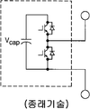
모듈러 멀티레벨 컨버터(M2LC) 토폴로지에 관한 많은 논문이 발표되어 왔다. 도 1은 2개의 단자를 갖는 M2LC 셀의 2-레벨 구성을 도시하고 있으며, 도 2는 2개의 단자를 갖는 M2LC의 3-레벨 구성을 도시하고 있고, 도 3은 M2LC 시스템을 도시하고 있다.Many articles have been published on modular multilevel converter (M2LC) topologies. Figure 1 shows a two-level configuration of a M2LC cell with two terminals, Figure 2 shows a three-level configuration of an M2LC with two terminals, and Figure 3 shows an M2LC system.
도 1에 도시된 바와 같이, M2LC 셀은 2개의 스위칭 디바이스, 2개의 다이오드, 캐패시터 및 2개의 단자를 포함한다. 도 1에 도시된 구성에서, 2개의 스위칭 디바이스는 2개의 상이한 전위(가령, 0 볼트 또는 VCAP) 중 하나가 2개의 단자 양단에 걸릴 수 있도록 제어될 수 있다. 도 2에 도시된 바와 같이, M2LC 셀은 4개의 스위칭 디바이스, 4개의 다이오드, 2개의 캐패시터 및 2개의 단자를 포함한다. 도 2에 도시된 구성에서, 4개의 스위칭 디바이스는 3개의 상이한 전위(가령, 0 볼트, VCAP 또는 2VCAP) 중 하나가 2개의 단자 양단에 걸릴 수 있도록 제어될 수 있다. M2LC 셀의 다른 토폴로지가 가능하지만, 토폴로지 전부는 스위칭 디바이스의 상태에 의존하여 2개의 단자 사이에서 다양한 레벨의 전압을 발생시킬 수 있는 내부 캐패시터 에너지 스토리지를 갖는 2-단자 서브시스템 또는 셀로서 정의될 수 있다.As shown in FIG. 1, an M2LC cell includes two switching devices, two diodes, a capacitor, and two terminals. In the configuration shown in Fig. 1, two switching devices can be controlled such that one of two different potentials (e.g., zero volts or V CAP ) can be applied across two terminals. As shown in FIG. 2, the M2LC cell includes four switching devices, four diodes, two capacitors, and two terminals. In the configuration shown in FIG. 2, the four switching devices can be controlled such that one of three different potentials (e.g., 0 volt, V CAP, or 2V CAP ) can be applied across two terminals. Although different topologies of the M2LC cell are possible, all of the topologies can be defined as a two-terminal subsystem or cell with an internal capacitor energy storage capable of generating varying levels of voltage between the two terminals depending on the state of the switching device. have.
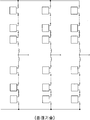
도 3에 도시된 바와 같이, M2LC 시스템은 복수의 M2LC 셀(서브시스템)을 포함하는 3상 브릿지로서 구성될 수 있는데, 여기서 M2LC 셀은 3개의 출력 상 모듈로서 배열된다. 물론, 다른 M2LC 시스템은 도 3에 도시된 바와 달리 구성될 수 있다. 예를 들어, 다른 M2LC 시스템은 2개의 출력 상 모듈로서 구성될 수 있다. 도 3의 M2LC 시스템에 있어서, 각 출력 상 모듈은 복수의 직렬 접속 M2LC 셀을 포함하며, 각 출력 상 모듈은 또한 포지티브 암(또는 밸브) 및 네거티브 암(또는 밸브)으로 배열되는데, 각 암(또는 밸브)은 유도성 필터에 의해 분리될 수 있다. 각 출력 상 모듈은 폴(a pole)로서 고려될 수 있다. 각 유도성 필터는 M2LC 시스템의 하나 보다 많은 폴이 하나의 공통 DC 버스상에서 병렬인 경우에 M2LC 토폴로지에서 사용된다. 유도성 필터는 M2LC 시스템의 암의 스위칭에 의해 발생되는 전류를 감소시키도록 동작한다. 암 전류의 스펙트럼 성분은 스위치 동작(switch function)과 폴의 출력 전류의 함수로 도시될 수 있다. M2LC 시스템의 일부 실시예는, 상대적으로 큰 인덕턴스를 갖는 유도성 필터와 함께 암 전류의 질을 최종적으로 제어하는 활동 폴 전류 제어기를 사용한다.As shown in FIG. 3, the M2LC system may be configured as a three-phase bridge comprising a plurality of M2LC cells (subsystems), wherein the M2LC cells are arranged as three output phase modules. Of course, other M2LC systems may be configured differently from those shown in FIG. For example, other M2LC systems may be configured as two output phase modules. In the M2LC system of Figure 3, each output phase module comprises a plurality of series connected M2LC cells, each output phase module also being arranged in a positive arm (or valve) and a negative arm (or valve) Valve) may be separated by an inductive filter. Each output phase module can be considered as a pole. Each inductive filter is used in the M2LC topology where more than one pole of the M2LC system is parallel on one common DC bus. The inductive filter operates to reduce the current generated by the switching of the arm of the M2LC system. The spectral component of the dark current can be plotted as a function of the switch function and the output current of the pole. Some embodiments of the M2LC system use an active pole current controller that ultimately controls the quality of the dark current with an inductive filter having a relatively large inductance.
간략히 하기 위해 도 1 내지 3에는 도시되어 있지 않지만, 각 M2LC 셀은 로컬 제어기도 포함하며, 각 로컬 제어기는 M2LC 시스템의 상위 레벨 제어기(가령, 허브 제어기)에 통신 가능하게 접속될 수 있다는 것을 인식할 것이다.Although not shown in Figures 1-3 for the sake of brevity, each M2LC cell also includes a local controller, which recognizes that each local controller can be communicatively connected to an upper level controller (e.g., hub controller) of the M2LC system will be.
M2LC 토폴로지는, 이것이 모듈러이며 각 암의 하나 이상의 중복 셀을 추가하는 기능으로 인해 높은 동작 이용 가능성이 가능하다는 점에서 캐스케이드형 H 브릿지(CCH) 토폴로지의 장점을 갖는다는 것을 인식할 것이다. 또한, M2LC 토폴로지는 버스 구성에 공적으로 적용될 수 있다. M2LC와 달리, CCH는 입력 에너지를 셀에 공급하는 개별적인 보조 와인딩을 포함하는 멀티-와인딩 변환기의 사용을 요구한다.The M2LC topology will recognize that this is modular and has the advantage of a cascaded H bridge (CCH) topology in that high operational availability is possible due to the ability to add one or more redundant cells of each arm. In addition, the M2LC topology can be applied to the bus configuration publicly. Unlike M2LC, the CCH requires the use of a multi-winding converter that includes individual auxiliary windings that supply input energy to the cell.
그러나, CCH와는 달리, M2LC 셀은 격리된 전압원 또는 보조 와인딩으로부터 독립적으로 공급되지 않는다. 소정의 M2LC 셀에 있어서, 2개의 단자 중 하나에서의 에너지 출력의 양은 2개의 단자 중 다른 하나에서의 에너지 입력의 양에 의존하며, 에너지를 저장하고 방출하는 셀의 능력에도 어느 정도 의존한다. 이는, 셀 중 하나 이상이 바이패싱되거나 비활성화될 때 전력 회로의 사전 충전 동안 또는 비정상적 동작 동안에 이들 셀에서 DC 링크 전압을 제어하는 데에 문제를 야기할 수 있다.However, unlike the CCH, the M2LC cell is not supplied independently from the isolated voltage source or auxiliary winding. For a given M2LC cell, the amount of energy output at one of the two terminals depends on the amount of energy input at the other of the two terminals, and also to some extent on the ability of the cell to store and emit energy. This can cause problems in controlling the DC link voltage in these cells during precharging or abnormal operation of the power circuit when one or more of the cells are bypassed or deactivated.
M2LC 시스템의 허브 제어 시스템으로부터 능동적으로 DC 링크 전압의 평형을 맞추는 다양한 방법이 채택되어 왔으나 이러한 방법은 (추가 셀 또는 부분적으로 변조된 셀의 형태로) 과도한 서브-시스템 또는 셀 용량을 요구한다. 또한, 이러한 방법은, 각 서브시스템 링크 전압의 진행 중인 모니터링을 요구하며, 상대적 DC 링크 전압 및 출력 전류 레벨의 방향 및 크기에 의존하여 변조를 위한 특정 셀을 선택하는 복잡한 분류 시스템의 사용을 요구한다는 점에서 상대적으로 복잡하다. 또한, 이러한 방법은 낮은 출력 전류 레벨 및 주파수에서 성능이 떨어지는 경향이 있으며, 캐패시터 전압의 평형을 맞추는 데에 필요한 전하를 공급하기 위해 부하가 접속되고 전류가 도전될 것을 요한다.Various methods have been adopted to actively balance the DC link voltage from the hub control system of the M2LC system, but this method requires excessive sub-system or cell capacity (in the form of an additional cell or a partially modulated cell). This method also requires ongoing monitoring of each subsystem link voltage and requires the use of a complex classification system that selects a particular cell for modulation depending on the direction and magnitude of the relative DC link voltage and output current level It is relatively complicated in point. This approach also tends to degrade performance at low output current levels and frequencies and requires that the load be connected and the current be challenged to supply the charge needed to balance the capacitor voltage.
또한, 셀 바이패스를 구현하는 다양한 방법이 채택되어 왔는데, 이는 도 3의 M2LC 시스템에 중복 셀이 추가될 것을 요구한다. 이 방법은, 하나의 추가 셀 행(랭크), 2개의 추가 셀 행 등을 출력 상 모듈의 포지티브 암 및 네거티브 암 모두에 추가하고 정상 조건 하에서 요구되는 정상 수의 랭크와 함께 중복 셀을 동작시킴으로써, 중복 셀이 n+1 리던던시, n+2 리던던시 등을 제공할 것을 요구한다. 이러한 방법을 사용하면, 한 암에서 특정 셀(가령 위상 A의 포지티브 암의 한 셀)에 장애가 발생하면, 그 셀은 스위치(도시 생략)에 의해 단락되어 장애가 발생한 셀을 "0" 상태로 두고, 보상 셀(가령, 위상 A의 네거티브 암의 한 셀)이 "1" 상태로 되어 전압의 평형을 다시 맞춤으로써 소정 출력 상 모듈의 모든 셀 전압의 합이 총 DC 링크 전압과 같게 된다. 출력 전압을 평형이 맞춰진 상태로 유지하기 위해, 이들 방법은 (가령, B 및 C 위상의 폴에서 요구되는 대로) 다른 출력 상 모듈에서와 같이 셀을 단락시키고 "1" 상태로 두는 것을 복제하여, 선간 전압으로의 출력이 고조파에 의해 영향받지 않게 한다.In addition, various methods of implementing cell bypass have been adopted, which require redundant cells to be added to the M2LC system of FIG. This method adds one additional cell row (rank), two additional cell rows, etc. to both the positive arm and the negative arm of the output phase module and operates the redundant cell with the normal number of ranks required under normal conditions, The redundant cell is required to provide n + 1 redundancy, n + 2 redundancy, and the like. With this method, when a fault occurs in a certain cell (e.g., one cell of the positive arm of phase A) in one arm, the cell is short-circuited by a switch (not shown) The sum of all the cell voltages of the predetermined output phase module becomes equal to the total DC link voltage by resetting the equilibrium of the voltage by setting the compensation cell (for example, one cell of the negative arm of the phase A) to the "1" In order to keep the output voltage balanced, these methods duplicate that the cells are shorted and left in a "1" state, as in other output phase modules (e.g., as required in the B and C phase poles) So that the output to the line voltage is not affected by harmonics.
그러나, 이러한 방법은 다양한 결점을 갖는데, 그 중 2개를 후술한다. 첫째, 보상 셀(단락된 셀의 반대되는 셀)에서 보상 "1"을 두는 것은 일정한 "1" 상태를 포함하는 셀의 개별적인 DC 링크에서 현저한 전압 리플이 발생하게 한다. 셀 중복 레벨을 증가시키기 위해 추가되는 랭크의 수가 많아질수록 전압 리플이 현저하게 악화된다. 둘째, 셀 전부, 요구되는 정상 수의 셀과 중복 셀 모두가 정상 조건 하에서 동작하도록 요구하는 것은, 요구되는 최소 수의 셀이 셀 바이패스 옵션이 없는 경우의 정상적인 효율 및 KVA 레이팅에 비해 M2LC 시스템의 효율 감소 및 M2LC 시스템의 KVA 레이팅 증가를 야기한다.
However, this method has various drawbacks, two of which are described below. First, putting the compensation "1" in the compensation cell (the opposite cell of the shorted cell) causes a significant voltage ripple to occur in the individual DC link of the cell that contains a certain "1 " state. As the number of ranks added to increase the cell redundancy level increases, the voltage ripple deteriorates noticeably. Second, requiring all of the cells, the required number of normal cells and the redundant cells to operate under normal conditions, means that the minimum number of cells required is less than the normal efficiency and KVA rating in the absence of the cell bypass option, Resulting in reduced efficiency and increased KVA rating of the M2LC system.
공지된 M2LC 시스템을 사용하는 것과 관련되는 추가적인 쟁점은, 낮은 출력 주파수에서 수용 가능한 동작 및 충분한 DC 출력 전류를 생성하는 기능을 포함한다. 이들 수행 특성은, 특히 M2LC 시스템이 높은 시작 토크 애플리케이션을 위한 AC 모터 제어를 위해 사용되는 경우에 매우 중요할 수 있다. CCH 토폴로지 등에서와 같은 셀에 공급하는 외부 전압원이 없기 때문에, 출력 기본 전류는 셀 및 에너지 저장 디바이스에서 완전하게 유지되어야 한다. 캐패시터 또는 콘덴서의 임피던스는 출력 주파수의 감소에 따라 단조적으로 증가한다는 것이 잘 알려져 있으므로, M2LC 셀의 최종 피크 리플 전압은 레이팅된 전류 조건 하에서도 낮은 주파수에서 손상 레벨을 초과할 수 있다. 마찬가지로, 브러시리스 또는 동기식 모터 애플리케이션을 시작하는 데에 중요한, DC 전류를 생성하는 M2LC 시스템의 기능은 알려진 제어 기술을 사용하는 M2LC 시스템으로는 달성하기 어렵다.
An additional issue associated with using the known M2LC system includes the ability to generate acceptable operation and sufficient DC output current at low output frequencies. These performance characteristics can be very important, especially when the M2LC system is used for AC motor control for high starting torque applications. Since there is no external voltage source to supply to the cell, such as in the CCH topology, the output base current must be maintained completely in the cell and energy storage device. It is well known that the impedance of a capacitor or capacitor increases monotonically with decreasing output frequency, so that the final peak ripple voltage of the M2LC cell may exceed the damage level at low frequencies even under rated current conditions. Likewise, the ability of a M2LC system to generate DC currents, important for starting brushless or synchronous motor applications, is difficult to achieve with M2LC systems using known control techniques.
본 발명의 다양한 실시예를 다음의 도면을 참조하여 예시적으로 설명한다. 도면에서 동일한 참조 번호는 동일 또는 유사한 요소를 지칭한다.
도 1은 2개의 단자를 갖는 M2LC 셀의 2-레벨 구성을 도시하고 있다.
도 2는 2개의 단자를 갖는 M2LC 셀의 3-레벨 구성을 도시하고 있다.
도 3은 복수의 M2LC 셀을 갖는 M2LC 시스템을 도시하고 있다.
도 4는 복수의 M2LC 서브시스템을 갖는 M2LC 시스템의 다양한 실시예를 도시하고 있다.
도 5는 다양한 실시예에 따른 도 4의 M2LC 시스템의 시스템 제어 모듈의 상위 레벨 표현을 도시하고 있다.
도 6은 다른 실시예에 따른 도 4의 M2LC 시스템의 시스템 제어 모듈의 상위 레벨 표현을 도시하고 있다.
도 7은 또 다른 실시예에 따른 도 4의 M2LC 시스템의 시스템 제어 모듈의 상위 레벨 표현을 도시하고 있다.
도 8은 M2LC 시스템의 3-레벨 M2LC 셀에 접속되는 듀얼 IGBT 바이패스를 포함하는 M2LC 시스템의 다양한 실시예를 도시하고 있다.
도 9는 도 4의 M2LC 시스템의 폴의 간략화된 표현을 도시하고 있다.
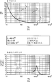
도 10은 M2LC 시스템의 유도성 필터가 제 1 인덕턴스 값을 갖는 경우에 도 4의 M2LC 시스템의 M2LC 폴의 폴 임피던스 및 캐패시터 전압 응답을 도시하고 있다.
도 11은 M2LC 시스템의 유도성 필터가 제 2 인덕턴스 값을 갖는 경우에 도 4의 M2LC 시스템의 M2LC 폴의 폴 임피던스 및 캐패시터 전압 응답을 도시하고 있다.Various embodiments of the present invention will now be described by way of example with reference to the following drawings. In the drawings, the same reference numerals refer to the same or similar elements.
Figure 1 shows a two-level configuration of a M2LC cell with two terminals.
Figure 2 shows a three-level configuration of a M2LC cell with two terminals.
3 shows an M2LC system having a plurality of M2LC cells.
Figure 4 illustrates various embodiments of an M2LC system having a plurality of M2LC subsystems.
FIG. 5 illustrates a high-level representation of a system control module of the M2LC system of FIG. 4 in accordance with various embodiments.
Figure 6 shows a high-level representation of a system control module of the M2LC system of Figure 4 according to another embodiment.
FIG. 7 illustrates a high-level representation of a system control module of the M2LC system of FIG. 4 in accordance with another embodiment.
Figure 8 shows various embodiments of an M2LC system including dual IGBT bypasses connected to a three-level M2LC cell of a M2LC system.
Figure 9 shows a simplified representation of the poles of the M2LC system of Figure 4;
Figure 10 shows the pole impedance and capacitor voltage response of an M2LC pole of the M2LC system of Figure 4 when the inductive filter of the M2LC system has a first inductance value.
Figure 11 shows the pole impedance and capacitor voltage response of the M2LC pole of the M2LC system of Figure 4 when the inductive filter of the M2LC system has a second inductance value.
본 발명의 도면 및 설명의 적어도 일부는 본 발명의 명확한 이해를 위해 관련되는 요소들을 설명하도록 간략화되었으며, 명확히 하기 위해 당업자가 본 발명의 일부를 구성한다고 인식할 다른 요소들을 소거하였다는 것을 이해해야 한다. 그러나, 이러한 요소들은 이 기술 분야에 잘 알려져 있고 본 발명의 보다 나은 이해를 돕지 않기 때문에, 이러한 요소들은 본 명세서에서 설명되지 않는다.It is to be understood that at least some of the drawings and description of the present invention have been simplified to illustrate the elements involved for a clear understanding of the present invention, and that other elements that those skilled in the art would recognize will form part of the present invention for clarity. However, since these elements are well known in the art and do not aid a better understanding of the present invention, these elements are not described herein.
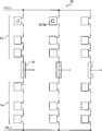
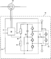
도 4는 복수의 M2LC 서브시스템(12)을 갖는 M2LC 시스템의 다양한 실시예를 도시하고 있다. M2LC 시스템(10)은 M2LC 서브시스템(12)이 출력 상 모듈로서 배치된다는 점에서 도 3의 M2LC 시스템과 유사하며, 각 출력 상 모듈은 포지티브 암(14) 및 네거티브 암(16)으로 배치된다.Figure 4 shows various embodiments of an M2LC system having a plurality of
그러나, 보다 상세히 후술할 바와 같이, 도 3의 M2LC 시스템과 대조적으로, 도 3의 M2LC 시스템(10)의 출력 상 모듈은 도 3의 M2LC 시스템의 출력 모듈의 인덕턴스보다 훨씬 작은 인덕턴스의 전체 값을 정의한다. 예를 들어, 다양한 실시예에 따르면, 도 4의 M2LC 시스템(10)의 출력 상 모듈에 대한 인덕턴스의 전체 값은 도 3의 M2LC 시스템의 출력 상 모듈의 인덕턴스보다 대략 40 내지 50 배 작다. 도 4의 M2LC 시스템(10)의 출력 상 모듈에 있어서, "보다 작게" 결정론적으로 정의되는 인덕턴스의 전체 값은, 시스템 제어 모듈(SCM)로 하여금 각 M2LC 서브시스템의 캐패시터 전압의 평형을 자동으로 맞추고 기본 캐패시터 전압 리플을 최소화하는 방식으로 M2LC 시스템(10)을 제어하게 한다. 도 4에는 시스템 제어 모듈(SCM)이 각 M2LC 서브시스템(12)(명확히 하기 위해 단 하나의 SCM만이 도시됨)에 존재하는 것으로 도시되어 있지만, 다른 실시예에 따르면 시스템 제어 모듈은 M2LC 시스템(10)의 상위 레벨 제어기(가령, 허브 제어기)에 존재할 수 있다는 것은 인식할 것이다. 시스템 제어 모듈의 다양한 실시예를 보다 상세히 후술할 것이다.However, as will be described in more detail below, in contrast to the M2LC system of FIG. 3, the output phase module of the
M2LC 시스템(10)의 소정 출력 상 모듈에 의해 정의되는 인덕턴스의 전체 값은 임의의 수의 상이한 방식으로 실현될 수 있다. 예를 들어, 다양한 실시예에 따르면, 인덕턴스의 전체 값은 포지티브 암과 네거티브 암(14, 16) 사이에 접속되는 결정론적으로 크기가 정해진 유도성 필터(18)를 포함함으로써 실현될 수 있다. 도 4에는 유도성 필터(18)가 출력 상 모듈의 포지티브 암과 네거티브 암(14, 16) 사이에 접속되는 2개의 인덕터를 갖는 것으로 도시되어 있지만, 유도성 필터(18)는 출력 상 모듈의 포지티브 암과 네거티브 암(14, 16) 사이에 접속되는 임의의 수의 인덕터(가령, 1개, 2개, 3개, 4개 등)를 가질 수 있다는 것을 인식할 것이다. 출력 상 모듈의 포지티브 암과 네거티브 암(14, 16) 사이에 1개, 2개, 3개, 4개 등의 인덕터가 접속되는지와 무관하게, 개별적인 인덕터는 결정론적으로 크기가 정해져서 출력 상 모듈의 전체 인덕턴스는 인덕턴스의 원하는 전체 값과 동일하게 됨으로써, 각 M2LC 서브시스템(12)의 캐패시터 전압의 평형을 자동으로 맞추고 기본 캐패시터 전압 리플을 최소화하는 방식으로 시스템 제어 모듈(SCM)이 M2LC 시스템(10)을 제어할 수 있다. The total value of the inductance defined by the predetermined output module of the
다른 실시예에 따르면, 인덕턴스의 전체 값은 출력 상 모듈의 M2LC 서브시스템(12) 중 하나 이상 사이에 분배되는, 하나 이상의 결정론적으로 크기가 정해지는 인덕터를 포함함으로써 실현될 수 있다. 이 배치는 포지티브 암과 네거티브 암(14, 16) 사이에 접속되는 유도성 필터(18)를 대신하여 또는 이와 관련하여 수행될 수 있다. 하나 이상의 보다 작은, 결정론적으로 크기가 정해진 인덕터는 출력 상 모듈의 복수의 M2LC 서브시스템(12)의 출력 단자에 접속될 수 있다. 이들 실시예에 있어서, 출력 상 모듈의 총 인덕턴스를 합하면 원하는 인덕턴스 값이 되어, 시스템 제어 모듈(SCM)은 각 M2LC 서브시스템(12)의 캐패시터 전압의 평형을 자동으로 맞추고 기본 캐패시터 전압 리플을 최소화하는 방식으로 M2LC 시스템(10)을 제어할 수 있다. 따라서, 인덕턴스의 원하는 값은, 가령, 인덕터가 포지티브 암과 네거티브 암(14, 16) 사이에 접속되는지, 인덕터가 M2LC 서브시스템(12) 사이에서 분배되든지, 인덕터가 복수의 M2LC 서브시스템(12)의 출력 단자에 접속되든지, 사용되는 인덕터의 수와 무관하게 실현될 수 있다는 것을 인식할 것이다.According to another embodiment, the total value of the inductance may be realized by including one or more deterministically sized inductors distributed between one or more of the
또 다른 실시예에 따르면, 인덕턴스의 전체 값은 출력 상 모듈의 기생 인덕턴스에 의해서만 실현될 수 있다. 이러한 실시예에서, 출력 상 모듈의 임의의 "추가적인" 인덕터를 포함할 필요가 없을 수 있으므로, M2LC 서브시스템(12)의 캐패시턴스의 양 감소 및 M2LC 서브시스템(10)의 전체 비용 감소를 허용한다. 인덕턴스의 전체 값을 출력 상 모듈/폴에 관해 설명하였지만, 각 암의 총 인덕턴스는 전술한 실시예들 중 하나 이상을 사용하여서도 결정론적으로 실행될 수 있다는 것을 인식할 것이다.According to another embodiment, the total value of the inductance can be realized only by the parasitic inductance of the output phase module. In this embodiment, it may not be necessary to include any "additional" inductors in the output phase module, thus allowing a reduction in the amount of capacitance of the
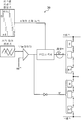
도 5는 다양한 실시예에 따른 M2LC 시스템(10)의 시스템 제어 모듈(20)의 상위 레벨 표현을 도시하고 있다. 간략히 하기 위해, M2LC 시스템의 일부만이 도 5에 도시되어 있다. 시스템 제어 모듈(20) (또는 그 기능적 균등물)은, 각 출력 상 모듈의 인덕턴스의 정의된 전체 값이 유효 암 캐패시턴스를 사용하여 적합하게 크기가 정해져서, (1) 각 출력 상 모듈의 임피던스를 충분히 낮게 하여 스위치 동작의 스위치 "재할당"(보다 상세히 후술함)의 낮은 레이트를 허용하여 M2LC 서브시스템(12)의 캐패시터 전압의 평형을 자동으로 맞추고, (2) 스위칭 주파수에 대해 공진 주파수를 충분히 높게 하여 스위칭 디바이스의 위상 제어가 어느 정도의 2-레벨 동작(보다 상세히 후술함)을 허용하여 M2LC 서브시스템(12)의 캐패시터의 기본 전류 성분의 대부분을 무효화하게 하는 경우, 다른 M2LC 시스템과 관련되는 전압 평형 및 기본 출력 주파수 리플 전압 결함을 최소화하는 방식으로 M2LC 시스템(10)을 제어하도록 사용될 수 있다. 이 2-레벨 동작은 각 암의 M2LC 서브시스템(12)이 0 볼트 상태에서 충분한 시간을 소비하고 플러스(+) 버스 또는 마이너스 버스(-)에 충분할 길이로 접속되어 기본 암 전류가 다른 위상을 무효화한다는 것을 암시하는 것임을 인식할 것이다. 이를 실현하기 위해, 폴 인덕턴스 및 직렬 암 캐패시턴스에 의해 형성되는 폴의 공진 주파수(도 9 참조)는 스위치 동작의 스위칭 주파수보다 커야 한다.FIG. 5 illustrates a high-level representation of the
시스템 제어 모듈(20)은 하드웨어, 펌웨어, 소프트웨어 및 그 조합으로 구현될 수 있으며, M2LC 시스템의 상위 레벨 제어기에 존재할 수 있다. 다른 실시예에 따르면, 시스템 제어기 모듈(20)은 각 M2LC 서브시스템(12)의 로컬 제어기(가령, 도 8의 제어기(56) 참조)에 존재할 수 있다. 소프트웨어를 사용하는 실시예에 있어서, 소프트웨어는 임의의 적합한 컴퓨터 언어(가령, C, C++, Java, JavaScript, Visual Basic, VBScript, Delphi)를 사용할 수 있으며, 임의의 유형의 머신, 컴포넌트, 물리적 또는 가상 장비, 저장 매체 또는 인스트럭션을 디바이스에 전달할 수 있는 전파 신호에 영구적으로 또는 임시로 포함될 수 있다. 시스템 제어 모듈(20)이 소프트웨어(가령, 소프트웨어 애플리케이션, 컴퓨터 프로그램)로 구현되는 실시예에 있어서, 소프트웨어는 컴퓨터 판독 가능한 매체(가령, 디스크, 디바이스 및/또는 전파 신호)상에 저장되어 컴퓨터가 이 매체를 판독하여 본 명세서에서 설명되는 기능이 수행될 수 있다.The
도 5에 도시된 바와 같이, 제어 시스템 모듈(20)의 기능은 M2LC 또는 CCH와 같은 멀티레벨 시스템용으로 사용되는 통상적인 삼각 PWM 변조기의 적응이다. 도 5에 도시된 상위 레벨 표현은 스위치 "재할당" 및 상대적 2-레벨 동작의 성능 특성을 도시하고 있다. 통상적인 PWM 변조기와 대조적으로, 제어 시스템 모듈(20)은, 소정 출력 상 모듈의 포지티브 암(14) 또는 네거티브 암(16)을 포함하는 "n"개의 M2LC 서브시스템(12)에 대한 "n"개의 별도의 존재 동작(existence function)을 생성하는 서브시스템 시퀀스 생성기의 기능을 포함한다. 서브시스템 시퀀스 생성기는 각 기능이 반복되는 전체 주기를 정의하는 가변적인 "레이트"에 의해 제어될 수 있다.As shown in FIG. 5, the function of the
또한, 통상적인 PWM 변조기와는 대조적으로, 2∏/n의 값만큼 정상적으로 이격된 삼각 파형 세트인 삼각파 생성기의 기능은 0과 1 사이에서 변할 수 있는 추가적인 가변 "오메가"를 사용한다. 따라서 이 실시예에 있어서, 삼각 파형들 간의 간격은 "(2∏/n) × (오메가)"의 값으로 표현될 수 있다. 가변 "오메가"는 각 삼각 파형의 상대적 위상 변위를 제어하여, "오메가" = 1일 때 삼각 파형이 출력 상 모듈로부터 낮은 출력 전압 왜곡에 대해 최적으로 이격되게 한다. "오메가" = 0이면, 이들 삼각 파형은 0 위상 시프트를 생성하여 M2LC 시스템(10)의 출력 상 모듈이 2-레벨 브릿지와 같이 전환하게 한다.Also, in contrast to a conventional PWM modulator, the function of the triangle generator, which is a set of triangular waveforms normally spaced by a value of 2? / N, uses an additional variable "omega" Therefore, in this embodiment, the interval between the triangular waveforms can be expressed by a value of "(2π / n) × (omega)". The variable "omega" controls the relative phase shift of each triangular waveform so that when "omega" = 1 the triangular waveform is optimally spaced from the output phase module for low output voltage distortion. If "omega" = 0, then these triangular waveforms produce a zero phase shift, causing the output phase module of the
M2LC 시스템(10)이 높은 전류 및 낮은 출력 주파수를 생성해야 하는 애플리케이션에 대해 낮은 값(가령, 0.1)이도록 오메가가 제어될 수 있다. 오메가를 이러한 값으로 제어하여, M2LC 서브시스템(12)의 캐패시터 전압의 평형을 맞추기 위한 스위치 "재할당"의 원하는 효과는 여전히 유효하며, 암(16, 18)은 캐패시터의 기본 전류 성분을 무효화하기 위해 필요한 시간(폴 공진 주파수의 주기보다 길 시간이라고 가정함)동안 플러스(+) 버스 또는 마이너스 (-) 버스에 각각 접속되어, 낮은 변조 레벨에서, 선간 전압에 대한 멀티레벨 라인은 오메가가 1로 설정된 경우와 같거나 그 이상일 수 있다. 또한, 이 상대적 2-레벨 모드에서 동작함으로써 M2LC 시스템(10)이 소정 애플리케이션을 위해 필요할 수 있는 DC 전류의 현저한 값을 생성하게 한다.The omega can be controlled to be a low value (e.g., 0.1) for applications where the
또한, 종래 PWM 변조기와는 대조적으로, 서브시스템 시퀀스 생성기의 기능은 포지티브 암(14)의 M2LC 서브시스템(12)에 적용되는 변조된 스위치 동작 "h+"가 가변 "레이트"에 의해 정의되는 주기로 "재할당"되게 하는 멀티플렉서를 피딩한다(feeds). 도 5에 도시된 실시예에 있어서, 네거티브 암(16)의 M2LC 서브시스템(12)과 연관되는 스위치 동작 "재할당"이 존재하지 않는다. 그러나, 다른 실시예에 따르면, 스위치 동작 "재할당"은 포지티브 암(14)의 M2LC 서브시스템(12)을 사용하는 대신에 네거티브 암(16)의 M2LC 서브시스템(12)을 사용하여 수행될 수 있다는 것을 인식할 것이다. 이는, M2LC 서브시스템(12) 중 하나가 에너지 저장 디바이스가 전하를 잃게 할 수 있는 M2LC 서브시스템 레이팅의 현저한 백분율의 손실 요소를 포함하는 경우에도 각 암의 M2LC 서브시스템(12)의 캐패시터 전하가 평형을 맞추도록 강제하는 이 "재할당" 효과이다.Further, in contrast to the conventional PWM modulator, the function of the subsystem sequence generator is such that the modulated switch operation "h + " applied to the
일반적으로, 도 5에 도시된 "재할당"이 수행되어, 출력 상 모듈의 포지티브 암(14)의 M2LC 서브시스템(12)의 수와 동일한 수의 주기가 완료된 후에, 변조된 스위치 동작의 값 각각은 출력 상 모듈의 포지티브 암(14)의 M2LC 서브시스템(12) 각각에 적용될 것이다.In general, "reallocation" is performed as shown in FIG. 5, so that after the number of cycles equal to the number of
"재할당"은 다수의 상이한 방식으로 구현될 수 있다는 것을 인식할 것이다. 예를 들어, 다양한 실시예에 따르면, 출력 상 모듈의 포지티브 암(14)의 3개의 M2LC 서브시스템(12)이 존재하는 경우, 주어진 주기 동안(가령, 주기 1)에, 변조된 스위치 동작의 제 1 값은 제 1 M2LC 서브시스템(12)에 적용되고, 변조된 스위치 동작의 제 2 값은 제 2 M2LC 서브시스템(12)에 적용되며, 변조된 스위치 동작의 제 3 값은 제 3 M2LC 서브시스템(12)에 적용된다. 다음 주기(가령, 주기 2) 동안에, 제 1 값은 제 2 M2LC 서브시스템(12)에 적용되고, 제 2 값은 제 3 M2LC 서브시스템(12)에 적용되며, 제 3 값은 제 1 M2LC 서브시스템(12)에 적용된다. 다음 주기(가령, 주기 3) 동안에, 제 1 값은 제 3 M2LC 서브시스템(12)에 적용되고, 제 2 값은 제 1 M2LC 서브시스템(12)에 적용되며, 제 3 값은 제 2 M2LC 서브시스템(12)에 적용된다. 전술한 재할당 시퀀스는 순환(rotation)이라 지칭될 수 있다.It will be appreciated that "reallocation" may be implemented in a number of different ways. For example, in accordance with various embodiments, if there are three
다른 실시예에 따르면, 순환이 아닌 "재할당"이 사용될 수 있다. 예를 들어, 출력 상 모듈의 포지티브 암(14)의 3개의 M2LC 서브시스템(12)이 존재하는 경우, 주어진 주기 동안(가령, 주기 1)에, 변조된 스위치 동작의 제 1 값은 제 1 M2LC 서브시스템(12)에 적용되고, 변조된 스위치 동작의 제 2 값은 제 2 M2LC 서브시스템(12)에 적용되며, 변조된 스위치 동작의 제 3 값은 제 3 M2LC 서브시스템(12)에 적용된다. 다음 주기(가령, 주기 2) 동안에, 제 1 값은 제 3 M2LC 서브시스템(12)에 적용되고, 제 2 값은 제 1 M2LC 서브시스템(12)에 적용되며, 제 3 값은 제 2 M2LC 서브시스템(12)에 적용된다. 다음 주기(가령, 주기 3) 동안에, 제 1 값은 제 2 M2LC 서브시스템(12)에 적용되고, 제 2 값은 제 3 M2LC 서브시스템(12)에 적용되며, 제 3 값은 제 1 M2LC 서브시스템(12)에 적용된다.According to another embodiment, a "reallocation" For example, if there are three
주어진 출력 상 모듈에서 사용하기 위한 멀티레벨 펄스 폭 변조(PWM) 방안이 도 5에 도시되어 있지만, 시스템 제어 모듈(20)은 다른 멀티 레벨 변조 제어 방안을 사용하여 전술한 스위치 동작 재할당 및 상대적 위상 제어를 실현할 수 있다는 것을 인식할 것이다. 예를 들어, 다양한 실시예에 따르면, 시스템 제어 모듈(20)은 시간 평균화 변조, 상태 공간 변조 등을 사용할 수 있다. 또한, 시스템 제어 모듈(20)은 다른 출력 상 모듈의 포지티브 암(또는 네거티브 암)에 대한 별도의 존재 동작 세트, 변조된 스위치 동작 세트 등을 생성할 수 있다는 것을 인식할 것이다.Although a multi-level pulse width modulation (PWM) scheme for use in a given output phase module is shown in FIG. 5, the
도 6은 다른 실시예에 따른 M2LC 시스템(10)의 제어 시스템 모듈(30)의 상위 레벨 표현을 도시하고 있다. 간략히 하기 위해, M2LC 시스템(10)의 일부만이 도 6에 도시되어 있다. 도 6의 제어 시스템 모듈(30)은 도 5의 제어 시스템 모듈(20)과 유사하지만, 도 6의 제어 시스템 모듈(30)은 2개의 서브시스템 시퀀스 생성기(포지티브 암을 위한 하나와 네거티브 암을 위한 하나)의 기능을 포함한다는 점에서 상이하다. 도 6에서, 네거티브 암 시퀀스 생성기에 의해 생성되는 "n"개의 존재 동작은 포지티브 암 시퀀스 생성기에 의해 생성되는 "n"개의 존재 동작으로부터 180도 시프트된다. 각 서브시스템 시퀀스 생성기는 상이한 멀티플렉서에 통신 가능하게 접속된다. 이는 두 암에서 비동기적으로 스위치 "재할당"을 허용한다(각 암의 스위치 동작은 동시에 재할당되지 않는다). 두 암의 재할당 레이트는 동일할 수 있지만 각 암 재할당 이벤트는 이격되어 동시에 발생하지 않게 한다. 예를 들어, 다양한 실시예에 따르면, 각 암 재할당 이벤트는 "레이트/2" 주기만큼 이격된다. 이 이격을 사용함으로써, 각 암의 전체 전압 평형이 향상된다. 또한, 이 이격은 M2LC 서브시스템 바이패스의 일부 버전을 위해 사용될 수 있는데, 바이패스 이벤트를 위해 보존이 유지되는 비동작 스위치 동작이 0 상태에서 재할당되지만 여전히 제어 시스템 모듈(30)의 전압 평형 기능을 허용할 수 있다. 다른 실시예에 따르면, 암 재할당들 사이의 이격의 값은 "레이트/2" 주기 이외의 다른 0이 아닌 값일 수 있다.6 shows a high-level representation of the
주어진 출력 상 모듈에서 사용하기 위한 멀티레벨 펄스 폭 변조(PWM) 방안이 도 6에 도시되어 있지만, 시스템 제어 모듈(30)은 다른 멀티 레벨 변조 제어 방안을 사용하여 스위치 동작 재할당 및 전술한 상대적 위상 제어를 실현할 수 있다는 것을 인식할 것이다. 예를 들어, 다양한 실시예에 따르면, 시스템 제어 모듈(30)은 시간 평균화 변조, 상태 공간 변조 등을 사용할 수 있다. 또한, 시스템 제어 모듈(30)은 다른 출력 상 모듈의 포지티브 및 네거티브 암에 대한 별도의 존재 동작 세트, 변조된 스위치 동작 세트 등을 생성할 수 있다는 것을 인식할 것이다.Although a multi-level pulse width modulation (PWM) scheme for use in a given output phase module is shown in FIG. 6, the
도 7은 또 다른 실시예에 따른 M2LC 시스템(10)의 제어 시스템 모듈(40)의 상위 레벨 표현을 도시하고 있다. 간략히 하기 위해, M2LC 시스템(10)의 일부만이 도 7에 도시되어 있다. 도 7의 제어 시스템 모듈(40)은 도 6의 제어 시스템 모듈(30)과 유사하지만 도 7의 제어 시스템 모듈(40)은 바이패스 제어 기능을 포함한다는 점에서 상이하다. 도 7에 도시된 바와 같이, 각 M2LC 서브시스템(12)은 M2LC 서브시스템(12)의 2 단자 양단에 접속되는 대응 바이패스 스위치(가령, IGBT 바이패스)를 가질 수 있다.FIG. 7 shows a high-level representation of the
제어 시스템 모듈(40)은 도 4에 도시된 M2LC 인버터 토폴로지를 사용하여 M2LC 서브시스템 바이패스 옵션을 구현하는 특유한 방식을 제공한다. 바이패스 제어는, 추가되는 중복 셀 랭크의 수에 의존하여 모든 3개의 출력 상 모듈의 포지티브 및 네거티브 암 모두에서 일정한 "0" 상태를 생성하도록 동작한다. 예를 들어, 최소 n+1개의 중복을 위한 포지티브 및 네거티브 암에 1 랭크를 추가함으로써 제어 시스템 모듈(40)로 하여금 각 암의 k번째 M2LC 서브시스템에 일정한 "0"을 생성하게 한다. 그 후, 제어 시스템 모듈(40)은 모든 M2LC 서브시스템(12) 사이에 이 "0"을 재할당하여 M2LC 서브시스템(12)의 전부가 평균적으로 평형있게 충전되게 할 수 있다. 하나의 M2LC 서브시스템(12)(가령, 위상 A의 포지티브 암)에 실제 장애가 발생하면, 장애가 발생한 M2LC 서브시스템(12)은 바이패스 스위치(IGBT 바이패스)에 의해 물리적 "0" 상태로 강제되고, 시간에 따른 전압 손실은 그 암에서만 재할당된 "0"을 소거함으로써 대체될 것이다. 이 방식으로, 모든 다른 중복 M2LC 서브시스템(12)은 추가 M2LC 서브시스템(12)이 위상 A의 네거티브 암에서 장애가 발생하면 이용 가능하며, 위상 B 및 C의 포지티브 암 및 네거티브 암에서도 마찬가지 이다. 전술한 방식으로 M2LC 서브시스템 바이패스를 수행함으로써 낮은 주파수에서 높은 리플 전압의 부정적인 효과가 방지된다. 또한, 어떠한 최종 손실도 M2LC 서브시스템 바이패스 기능을 포함하지 않는 M2LC 시스템으로 경험하는 손실보다 현저하게 크지 않으며, M2LC 시스템의 최종 KVA 레이팅은 바이패스를 사용하지 않는 경우와 동일하다.The
도 7에서, 부호 "h+n"은 변조된 스위치 동작 "h+"의 n번째 값을 나타내고, 부호 "h-n"은 변조된 스위칭 기능 "h-"의 n번째 값을 나타낸다. 주어진 출력 상 모듈에서 사용하기 위한 멀티레벨 펄스 폭 변조(PWM) 방안이 도 7에 도시되어 있지만, 시스템 제어 모듈(40)은 다른 멀티 레벨 변조 제어 방안을 사용하여 전술한 스위치 동작 재할당 및 상대적 위상 제어를 실현할 수 있다는 것을 인식할 것이다. 예를 들어, 다양한 실시예에 따르면, 시스템 제어 모듈(30)은 시간 평균화 변조, 상태 공간 변조 등을 사용할 수 있다. 또한, 시스템 제어 모듈(40)은 다른 출력 상 모듈의 포지티브 및 네거티브 암에 대한 별도의 존재 동작 세트, 변조된 스위치 동작 세트 등을 생성할 수 있다는 것을 인식할 것이다.7, the symbol "h + n" represents the n-th value of the modulated switch operation "h +" and the symbol "h-n" represents the n-th value of the modulated switching function "h-". Although a multi-level pulse width modulation (PWM) scheme for use in a given output phase module is shown in FIG. 7, the
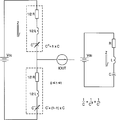
도 8은 M2LC 시스템(50)의 다양한 실시예를 도시하고 있다. 도 8의 M2LC 시스템(50)은 도 4의 M2LC 시스템(10)과 유사하지만 도 8의 M2LC 시스템(50)은 M2LC 시스템(50)의 3-레벨 M2LC 서브시스템(54)에 접속되는 바이패스 디바이스(52)를 포함한다는 점에서 상이하다. 간략히 하기 위해, M2LC 시스템(50)의 일부만이 도 8에 도시되어 있다. 그러나, M2LC 시스템(50)은 복수의 M2LC 서브시스템(54)을 포함하고 각 M2LC 서브시스템(54)은 자신에 접속되는 대응 바이패스 디바이스(52)를 가질 수 있다는 것을 인식할 것이다.FIG. 8 illustrates various embodiments of the
도 8에 도시된 바와 같이, M2LC 서브시스템(54)은 제어기(56), 밸러스트 저항(58), 캐패시터, 스위칭 디바이스 및 다이오드를 포함한다. 스위칭 디바이스는 임의의 적합한 유형의 스위칭 디바이스로서 구현될 수 있다. 예를 들어, 도 8에 도시된 바와 같이, 스위칭 디바이스는 IGBT(insulated gate bipolar transistors)로서 구현될 수 있다. 제어기(56)는 변류기(60)에 전기적으로 접속된다. 다양한 실시예에 따르면, 변류기(60)는 제어기(6)에 전력을 공급하고, 제어기(56)는 전력을 스위칭 디바이스의 각 게이트 단자에 공급한다. 간략히 하기 위해, 제어기(56)와 각 스위칭 디바이스의 게이트 단자 사이의 접속은 도 8에 도시되어 있지 않다. M2LC 시스템(50)의 M2LC 서브시스템(54) 각각에 대해, 각 M2LC 서브시스템(54)은 대응하는 변류기(60)에 전기 접속되고, 소정 M2LC 서브시스템(54)에 공급되는 전력은 하나의 대응하는 변류기(60)를 통해서만 공급될 수 있다는 것을 인식할 것이다. 또한, 제어기(56)는, 가령, 2개의 광 섬유를 통해 상위 레벨 제어기(가령, 허브 제어기)에 통신 가능하게 접속된다. 간략히 하기 위해, 상위 레벨 제어기는 도 8에 도시되어 있지 않다.As shown in FIG. 8, the
바이패스 디바이스(52)는 2개의 스위칭 디바이스를 포함하며, 2개의 스위칭 디바이스는 임의의 적합한 유형의 스위칭 디바이스로 구현될 수 있다. 다양한 실시예에 따르면, 2개의 스위칭 디바이스는 패키지된 IGBT 세트 또는 개별적인 IGBT로서 구현될 수 있고, IGBT는 3-레벨 M2LC 서브시스템(54)에 포함되는 IGBT와 동일한 전압 정격일 수 있다. 개별적으로 제어되는 듀얼 IGBT의 사용은, 중간점 저항(62)을 저장 캐패시터의 센터 탭(64)에 인가하여 3-레벨 M2LC 서브시스템(54)에서의 장애의 결과로서 요구되는 경우에, 듀얼 저장 캐패시터 각각의 독립적인 방전을 허용한다. 저항(62)은 3-레벨 M2LC 서브시스템(54) 회로를 단락하기 위해 동시에 IGBT 세트가 턴 온되기 전에 각 전류 경로를 방전하기 위해 사용될 수 있다. 또한, 저항(62)은 개별적인 DC 버스를 기준으로 각 바이패스 IGBT상에 전압이 공유되는 것을 보장하는 역할을 한다.
제어기(56)는 스위칭 디바이스의 캐패시터 및 비-게이트 단자에 밸러스트 저항(58)을 통해 간접적으로 전기 접속된다. 밸러스트 저항(58)은 임의의 적합한 유형의 밸러스트 저항일 수 있다. 밸러스트 저항(58) 및 제어기(56)는 집합적으로 기준점 "M"을 정의한다. 이러한 구성에서, 기준점 "M"에서의 전압은 저장 캐패시터의 센터 탭(64)에서의 전압과 상이할 수 있으며, 전류는 기준점 "M"으로부터 저장 캐패시터의 센터 탭(64)으로 직접 전도되지 않을 수 있고, 밸러스트 저항(58)의 높은 저항 성질은 공통 모드 전류가 제어기(56)의 접지 시스템으로 흐르는 것을 방지하도록 동작한다.The
도 9는 도 4의 M2LC 시스템(10)의 폴의 간략화된 표현을 도시하고 있다. 도 9에 도시된 바와 같이, M2LC 시스템(10)의 폴(Z)의 각 암은 가변 캐패시턴스를 갖는 각 공진 회로로서 표현될 수 있다. M2LC 폴의 암은 변조되어, 전체 스위치된 캐패시터 전압의 합은 전체 DC 링크 전압 Vdc와 같고, 변조(h) 값의 범위는 "0"과 "1" 사이이며, 각각 (h)의 함수인 2개의 암 캐패시턴스가 전체 암 캐패시턴스인 일정한 값 C에 효율적으로 조합되므로 각 공진 회로는 하나의 LRC 회로로 감소될 수 있다는 것을 인식할 것이다. 그러므로, M2LC 서브시스템 캐패시터 전압의 평형을 자동으로 맞추는 데에 있어서 시스템 제어 모듈(가령, 시스템 제어 모듈(20), 시스템 제어 모듈(30) 및 시스템 제어 모듈(40) 등)의 성능은 폴(Z)의 유효 임피던스에 의존하며, M2LC 서브시스템 캐패시터 기본 전류 성분의 대부분을 무효화하는 기능은 M2LC 서브시스템 스위칭 주파수의 레이트에 대한 폴의 공진 주파수에 의존한다는 것을 인식할 것이다. 이 임피던스는 각 게이트 기능 재할당 동안에 캐패시터가 충전 전류를 공유할 수 있도록 충분히 낮아야 하며, 또한, 2-레벨 토폴로지로 정상적으로 발생하는 각 M2LC 폴의 기본 전류가 부분적으로 무효화될 수 있게끔 변조가 (가령, 게이트 스위치 동작들 사이의 위상 시프트를 감소시킴으로써) 제어될 수 있도록 충분히 낮아야 한다.FIG. 9 shows a simplified representation of the poles of the
또한, M2LC 폴의 기본 동작 주파수 및 스위칭 주파수 모두보다 현저히 큰 값에서 유효 폴 캐패시턴스와의 자연 공진이 발생하도록 폴 인덕터의 크기가 충분히 작게 정해지면, 자연 공진은 정상 회로 손실에 의해 댐핑된 정상적인 기본 및 스위칭 주파수로부터 충분히 제거될 것이다.Also, if the size of the pole inductor is determined to be sufficiently small such that natural resonance with the effective pole capacitance occurs at a value significantly greater than both the fundamental operating frequency and the switching frequency of the M2LC pole, the natural resonance will be normal base and damped Will be sufficiently removed from the switching frequency.
도 10 및 11은 도 4의 M2LC 시스템(10)의 유도성 필터(18)가 제 1 인덕턴스 값(도 10) 및 제 2 인덕턴스 값(도 11)을 갖는 경우에 M2LC 시스템(10)의 M2LC 폴의 폴 임피던스 및 캐패시터 전압 응답을 각각 도시하고 있다. 도 10 및 11에 도시된 회로 값은 4.1 kv 1000 HP 3상 가변 주파수 드라이브에서 사용될 수 있는 실제 값을 나타낸다. 제 1 인덕턴스 값은 공지된 M2LC 시스템에서 통상적으로 사용되는 인덕턴스 값이다. 제 2 인덕턴스 값은 전술한 시스템 제어 모듈(가령, 시스템 제어 모듈(20), 시스템 제어 모듈(30), 시스템 제어 모듈(40) 등)에 의해 제어되는 M2LC 시스템에서 사용되는 인덕턴스 값이다.Figures 10 and 11 illustrate how the
도 10에 도시된 값에 있어서, 출력 전류 주파수(동작 주파수 "fo")는 통상적으로 공진 주파수 "fr"보다 작고, 스위칭 주파수 "fsw"는 통상적으로 공진 주파수 "fr"보다 크다. 그러나, 도 11에 도시된 값에 있어서, 공진 주파수 "fr"은 동작 주파수 "fo"보다 충분히 크고, 스위칭 주파수 "fsw"보다도 크다.10, the output current frequency (operating frequency "f o ") is typically less than the resonant frequency "f r " and the switching frequency "f sw " is typically greater than the resonant frequency "f r ". However, in the value shown in Fig. 11, the resonance frequency "f r " is sufficiently larger than the operating frequency "f o " and is larger than the switching frequency "f sw ".
제 1 인덕턴스 값과 제 2 인덕턴스 값을 비교함으로써, 전술한 제어 시스템 모듈과 함께 사용될 폴 인덕터의 인덕턴스 값이 종래 시스템에서 사용되는 폴 인덕터보다 대략 40 내지 50배 작다는 것을 인식할 것이다. 따라서, 전술한 제어 시스템 모듈과 함께 사용된 폴 인덕터와 관련되는 크기, 비용 및 손실이 종래 시스템에서 사용되는 폴 인덕터와 관련되는 크기, 비용 및 손실보다 현저하게 작다는 것도 인식할 것이다.By comparing the first inductance value and the second inductance value, it will be appreciated that the inductance value of the pole inductor to be used with the control system module described above is approximately 40 to 50 times smaller than the pole inductor used in prior art systems. Thus, it will be appreciated that the size, cost, and loss associated with the pole inductors used with the control system module described above are significantly less than the size, cost, and loss associated with the pole inductors used in prior art systems.
전술한 바로부터, 전술한 제어 시스템 모듈은, 기본 주파수 및 스위칭 주파수에 대한 폴 필터 임피던스 및 공진의 선택과 조합하여, M2LC 시스템의 상위 레벨 제어기(허브 제어)로부터의 복잡한 모니터링 및 제어 없이 전압 평형 및 리플 전압 감소가 달성되게 한다는 것은 인식할 것이다. 또한, 전술한 제어 시스템 모듈은 부하 전류 및 출력 전압이 없는 조건 하에서 DC 링크 전압의 전하 평형 동작을 강제할 수 있다는 것과, 제어 시스템 모듈은 DC 출력 전류의 생성, 낮은 출력 주파수에서의 리플 전압 제어 및 높은 중복에 대한 "제로" 전압 셀의 생성도 허용한다는 것을 인식할 것이다. 또한, 전술한 제어 시스템 모듈은, 각 암 사이에 배치되는 폴 인덕턴스(또는 M2LC 서브시스템(12)의 출력 단자에 접속되는 총 인덕턴스)가 유효 폴 캐패시턴스와의 공진이 M2LC 서브시스템(12)의 스위칭 주파수 및 동작 주파수 모두보다 충분히 높도록 충분히 낮은 경우에 이용 가능하다는 것도 인식할 것이다. 이렇게 함으로써, 전술한 시스템 제어 모듈(또는 그 기능적 균등물)은 다른 M2LC 토폴로지와 관련되는 낮은 출력 주파수 리플 전압 문제점을 해결하고, 모든 출력 동작 조건 하에서 전압의 평형을 맞추도록 M2LC 서브시스템(12)의 기능을 크게 간략화하고 개선시킬 수 있다.From the foregoing, the control system module described above, in combination with the selection of the pole filter impedance and resonance for the fundamental frequency and switching frequency, can be used for voltage balancing and control without complex monitoring and control from the upper level controller (hub control) It will be appreciated that ripple voltage reduction is achieved. It is also noted that the control system module described above can enforce the charge balancing operation of the DC link voltage under the absence of load current and output voltage and that the control system module is capable of generating DC output current, Quot; zero "voltage cell for high redundancy. In addition, the above-described control system module may be configured such that the pole inductance (or the total inductance connected to the output terminal of the M2LC subsystem 12) disposed between each arm is such that resonance with the effective pole capacitance results in the switching of the
전술한 내용은 본 발명의 어떠한 특정 재료, 기하구조 또는 요소 배치로 한정하도록 의도된 것이 아니다. 본 발명의 범위 내에서 많은 부분/배치 대체물을 고려할 수 있으며 이는 당업자에게 자명할 것이다. 본 명세서에서 설명되는 실시예는 예시를 위해 제공되었으며 본 발명의 범위를 제한하기 위해 사용되어서는 안 된다.The foregoing is not intended to be limited to any particular material, geometry or elemental arrangement of the present invention. Many portion / batch alternatives are contemplated within the scope of the present invention and will be apparent to those skilled in the art. The embodiments described herein are provided for illustrative purposes and should not be used to limit the scope of the invention.
본 발명은 본 출원의 특정 실시예와 관련하여 설명하였지만, 본 개시 내용을 참조하여 당업자는 청구되는 발명의 사상을 벗어나지 않고 범위를 초과하지 않으면서 추가적인 실시예 및 수정을 고려할 수 있다. 따라서, 본 명세서의 도면 및 설명은 본 발명의 이해를 돕기 위해서만 제공되는 것이며 그 범위를 한정하기 위한 것으로 고려되어서는 안 된다는 것을 이해해야 한다.Although the present invention has been described in connection with specific embodiments thereof, those skilled in the art, upon reference to the present disclosure, may contemplate additional embodiments and modifications without departing from the scope of the invention as claimed. It is, therefore, to be understood that the drawings and description herein are presented for the understanding of the present invention only and are not to be construed as limiting the scope thereof.
Claims (22)
적어도 2개의 출력 상 모듈(output phase modules)들로 배치되는 복수의 직렬 접속된 2-단자 M2LC 서브시스템들 ― 상기 출력 상 모듈들 중 제 1 출력 상 모듈은 인덕턴스의 전체 값을 정의하고, 포지티브 암 및 네거티브 암을 포함함 ― 과,
상기 출력 상 모듈들 중 상기 제 1 출력 상 모듈의 상기 2-단자 M2LC 서브시스템들에 통신 가능하게 접속되는 제어 시스템 모듈을 포함하되,
상기 제어 시스템 모듈은
상기 출력 상 모듈들 중 상기 제 1 출력 상 모듈의 상기 포지티브 암의 상기 2-단자 M2LC 서브시스템들과,
상기 출력 상 모듈들 중 상기 제 1 출력 상 모듈의 상기 네거티브 암의 상기 2-단자 M2LC 서브시스템들 중 하나에만
특정 시각에, 선택적으로 재할당되고 변조된 스위치 동작들(switch functions)을 적용하도록 구성되며,
상기 변조된 스위치 동작들의 선택적 재할당은, 사전 결정된 레이트로 상기 직렬 접속된 2-단자 M2LC 서브시스템들의 개별적인 캐패시터의 전하 평형을 강제하는
모듈러 멀티레벨 컨버터 시스템.A modular multi-level converter system,
A plurality of series connected two-terminal M2LC subsystems arranged in at least two output phase modules, wherein a first one of the output phase modules defines an overall value of the inductance, And a negative arm,
And a control system module communicatively coupled to the 2-terminal M2LC subsystems of the first output one of the output phase modules,
The control system module
Terminal M2LC subsystems of the positive arm of the first output phase module of the output phase modules,
Only one of the two-terminal M2LC subsystems of the negative arm of the first output phase module of the output phase modules
At a particular time, is adapted to apply selectively reassigned and modulated switch functions,
The selective reallocation of the modulated switch operations is performed by forcing the charge balance of the individual capacitors of the serially connected two-terminal M2LC subsystems at a predetermined rate
Modular multilevel converter system.
상기 출력 상 모듈들 중 상기 제 1 출력 상 모듈은, 상기 출력 상 모듈들 중 상기 제 1 출력 상 모듈의 유효 캐패시턴스와의 자연 공진 주파수가
상기 출력 상 모듈들 중 상기 제 1 출력 상 모듈의 동작 주파수와,
상기 출력 상 모듈들 중 상기 제 1 출력 상 모듈의 스위칭 주파수보다 크도록 구성되는
모듈러 멀티레벨 컨버터 시스템.
The method according to claim 1,
Wherein the first output phase module of the output phase modules has a natural resonance frequency with an effective capacitance of the first output phase module among the output phase modules
The operating frequency of the first output phase module of the output phase modules,
Wherein the first output phase module is configured to be greater than the switching frequency of the first output phase module
Modular multilevel converter system.
상기 출력 상 모듈들 중 상기 제 1 출력 상 모듈의 상기 포지티브 암과 상기 네거티브 암 사이에 접속되는 하나 이상의 인덕터들을 더 포함하는
모듈러 멀티레벨 컨버터 시스템.
The method according to claim 1,
And one or more inductors connected between the positive arm and the negative arm of the first output phase module of the output phase modules
Modular multilevel converter system.
상기 출력 상 모듈들 중 상기 제 1 출력 상 모듈의 상기 M2LC 서브시스템들 사이에 분배되는 하나 이상의 인덕터들을 더 포함하는
모듈러 멀티레벨 컨버터 시스템.The method according to claim 1,
Further comprising one or more inductors that are distributed between the M2LC subsystems of the first output phase module of the output phase modules
Modular multilevel converter system.
상기 하나 이상의 인덕터들은 상기 출력 상 모듈들 중 상기 제 1 출력 상 모듈의 상기 M2LC 서브시스템들 중 적어도 2개의 출력 단자들에 접속되는
모듈러 멀티레벨 컨버터 시스템.
5. The method of claim 4,
Wherein the one or more inductors are connected to at least two output terminals of the M2LC subsystems of the first output phase module of the output phase modules
Modular multilevel converter system.
상기 인덕턴스의 전체 값은 상기 출력 상 모듈을 포함하는 전기 회로의 기생 인덕턴스인
모듈러 멀티레벨 컨버터 시스템.
The method according to claim 1,
Wherein the total value of the inductance is a parasitic inductance of the electric circuit including the output phase module
Modular multilevel converter system.
상기 제어 시스템 모듈은 상기 출력 상 모듈들 중 상기 제 1 출력 상 모듈의 상기 2-단자 M2LC 서브시스템들에 상기 선택적으로 할당되고 변조된 스위치 동작들의 상대적 상 변위를 제어하도록 더 구성되는
모듈러 멀티레벨 컨버터 시스템.
The method according to claim 1,
The control system module is further configured to control the relative phase displacement of the selectively allocated and modulated switch operations to the 2-terminal M2LC subsystems of the first of the output phase modules
Modular multilevel converter system.
상기 제어 시스템 모듈은 2-레벨부터 n-레벨까지의 다양한 정도로 상대적 상 변위를 제어하도록 더 구성되며,
상기 n-레벨은, 상기 출력 상 모듈들 중 상기 제 1 출력 상 모듈의 각 암에 2-레벨 2-단자 M2LC 서브시스템들을 동작시키는 횟수에 의해 결정되는
모듈러 멀티레벨 컨버터 시스템.
8. The method of claim 7,
The control system module is further configured to control relative phase displacements to varying degrees from 2-level to n-level,
The n-level is determined by the number of times the two-level two-terminal M2LC subsystems operate on each arm of the first of the output phase modules
Modular multilevel converter system.
상기 제어 시스템 모듈은 변수의 값을 조절하여 상기 상대적 상 변위를 제어하도록 더 구성되되, 상기 값은 낮게는 0이고 높게는 1일 수 있는
모듈러 멀티레벨 컨버터 시스템.
8. The method of claim 7,
The control system module is further configured to control the relative phase displacement by adjusting the value of the variable, wherein the value may be 0 at low and 1 at high
Modular multilevel converter system.
상기 제어 시스템 모듈은 펄스 폭 변조기를 포함하는
모듈러 멀티레벨 컨버터 시스템.
The method according to claim 1,
Wherein the control system module comprises a pulse width modulator
Modular multilevel converter system.
상기 제어 시스템 모듈은 시간-평균화 변조기를 포함하는
모듈러 멀티레벨 컨버터 시스템.
The method according to claim 1,
Wherein the control system module comprises a time-averaging modulator
Modular multilevel converter system.
상기 제어 시스템 모듈은 상태-공간 변조기를 포함하는
모듈러 멀티레벨 컨버터 시스템.
The method according to claim 1,
The control system module includes a state-space modulator
Modular multilevel converter system.
상기 제어 시스템 모듈은 상기 2-단자 M2LC 서브시스템들 중 하나에 재할당 "0" 상태를 추가하도록 더 구성되는
모듈러 멀티레벨 컨버터 시스템.
The method according to claim 1,
The control system module is further configured to add a reallocated "0" state to one of the two-terminal M2LC subsystems
Modular multilevel converter system.
복수의 바이패스 디바이스를 더 포함하되, 각 바이패스 디바이스는 대응하는 2-단자 M2LC 서브시스템에 접속되는
모듈러 멀티레벨 컨버터 시스템.
The method according to claim 1,
Further comprising a plurality of bypass devices, each bypass device being connected to a corresponding two-terminal M2LC subsystem
Modular multilevel converter system.
상기 바이패스 디바이스 각각은 2개의 스위칭 디바이스를 포함하는
모듈러 멀티레벨 컨버터 시스템.
15. The method of claim 14,
Each of the bypass devices including two switching devices
Modular multilevel converter system.
상기 스위칭 디바이스는 절연 게이트 바이폴라 트랜지스터인
모듈러 멀티레벨 컨버터 시스템.
16. The method of claim 15,
The switching device is an insulated gate bipolar transistor
Modular multilevel converter system.
상기 스위칭 디바이스는 상기 2-단자 M2LC 서브시스템들의 스위칭 디바이스와 동일한 전압 정격을 갖는
모듈러 멀티레벨 컨버터 시스템.
16. The method of claim 15,
Wherein the switching device has the same voltage rating as the switching device of the two-terminal M2LC subsystems
Modular multilevel converter system.
상기 바이패스 디바이스 각각은 저항을 더 포함하되, 상기 저항은 특정 바이패스 디바이스에 있어서
상기 바이패스 디바이스의 상기 2개의 스위칭 디바이스의 공통 접속과,
상기 대응하는 2-단자 M2LC 서브시스템의 2개의 캐패시터의 공통 접속에 접속되는
모듈러 멀티레벨 컨버터 시스템.
16. The method of claim 15,
Wherein each of the bypass devices further comprises a resistor,
A common connection of the two switching devices of the bypass device,
Connected to a common connection of two capacitors of the corresponding two-terminal M2LC subsystem
Modular multilevel converter system.
상기 모듈러 멀티레벨 컨버터 시스템은 적어도 2개의 출력 상 모듈들로 배치되는 복수의 직렬 접속된 2-단자 M2LC 서브시스템들을 가지며,
상기 방법은
상기 출력 상 모듈들 중 제 1 출력 상 모듈의 암의 M2LC 서브시스템들에 제 1 세트의 위치 동작들을 적용하는 단계 - 상기 암의 각 M2LC 서브시스템은 상기 스위치 동작들 중 상이한 스위치 동작을 수신함 - 와,
상기 스위치 동작들의 각각이 상기 암의 상기 M2LC 서브시스템들의 각각에 적용될 때까지 상기 스위치 동작들을 재할당하는 단계를 포함하는
모듈러 멀티레벨 컨버터 시스템 제어 방법.
A method of controlling a modular multi-level converter system,
The modular multi-level converter system has a plurality of serially connected two-terminal M2LC subsystems arranged with at least two output phase modules,
The method
Applying a first set of positional operations to the M2LC subsystems of the arm of the first of the output phase modules, wherein each M2LC subsystem of the arm receives a different one of the switch operations; ,
And reassigning the switch operations until each of the switch operations is applied to each of the M2LC subsystems of the arm
A method of controlling a modular multilevel converter system.
상기 재할당하는 단계는, 상기 스위치 동작들의 각각이 상기 암의 상기 M2LC 서브시스템들의 각각에 적용될 때까지 상기 스위치 동작들을 회전시키는 단계를 포함하는
모듈러 멀티레벨 컨버터 시스템 제어 방법.
20. The method of claim 19,
Wherein the reallocating comprises rotating the switch operations until each of the switch operations is applied to each of the M2LC subsystems of the arm
A method of controlling a modular multilevel converter system.
상기 출력 상 모듈들 중 상기 제 1 출력 상 모듈의 다른 암의 M2LC 서브시스템들에 제 2 세트의 스위치 동작들을 적용하는 단계 - 상기 다른 암의 각 M2LC 서브시스템은 상기 제 2 세트의 스위치 동작들 중 상이한 스위치 동작을 수신함 - 와,
상기 제 2 세트의 스위치 동작들의 각각이 상기 다른 암의 상기 M2LC 서브시스템들의 각각에 적용될 때까지 상기 제 2 세트의 스위치 동작들을 재할당하는 단계를 더 포함하는
모듈러 멀티레벨 컨버터 시스템 제어 방법.
20. The method of claim 19,
Applying a second set of switch operations to the M2LC subsystems of the other arm of the first output phase module of the output phase modules, each M2LC subsystem of the other arm having a first set of switch operations Receiving different switch operations -
Further comprising reallocating the second set of switch operations until each of the second set of switch operations is applied to each of the M2LC subsystems of the other arm
A method of controlling a modular multilevel converter system.
상기 제 1 세트의 스위치 동작들은 상기 제 2 세트의 스위치 동작들과는 다른 시간에 적용되는
모듈러 멀티레벨 컨버터 시스템 제어 방법.22. The method of claim 21,
Wherein the first set of switch operations are applied at a different time than the second set of switch operations
A method of controlling a modular multilevel converter system.
Applications Claiming Priority (3)
| Application Number | Priority Date | Filing Date | Title |
|---|---|---|---|
| US38118010P | 2010-09-09 | 2010-09-09 | |
| US61/381,180 | 2010-09-09 | ||
| PCT/US2011/050902 WO2012033958A1 (en) | 2010-09-09 | 2011-09-09 | System and method for controlling a m2lc system |
Publications (2)
| Publication Number | Publication Date |
|---|---|
| KR20140051810A true KR20140051810A (en) | 2014-05-02 |
| KR101776984B1 KR101776984B1 (en) | 2017-09-08 |
Family
ID=45810975
Family Applications (1)
| Application Number | Title | Priority Date | Filing Date |
|---|---|---|---|
| KR1020137009095A KR101776984B1 (en) | 2010-09-09 | 2011-09-09 | System and method for controlling a m2lc system |
Country Status (6)
| Country | Link |
|---|---|
| US (1) | US8618698B2 (en) |
| EP (1) | EP2614567A4 (en) |
| JP (1) | JP5964306B2 (en) |
| KR (1) | KR101776984B1 (en) |
| CN (1) | CN103250318B (en) |
| WO (1) | WO2012033958A1 (en) |
Cited By (3)
| Publication number | Priority date | Publication date | Assignee | Title |
|---|---|---|---|---|
| KR101629397B1 (en) | 2015-12-03 | 2016-06-13 | 연세대학교 산학협력단 | Apparatus and Method for Controlling of Asymmetric Modular Multilevel Converter |
| WO2017115954A1 (en) * | 2015-12-31 | 2017-07-06 | 주식회사 효성 | Redundancy control method of mmc for statcom |
| WO2017115953A1 (en) * | 2015-12-31 | 2017-07-06 | 주식회사 효성 | Redundancy control method of mmc for hvdc |
Families Citing this family (40)
| Publication number | Priority date | Publication date | Assignee | Title |
|---|---|---|---|---|
| EP3659491A1 (en) | 2011-12-13 | 2020-06-03 | EndoChoice Innovation Center Ltd. | Removable tip endoscope |
| DE102012202173B4 (en) * | 2012-02-14 | 2013-08-29 | Siemens Aktiengesellschaft | Method for operating a multiphase, modular multilevel converter |
| WO2013134628A1 (en) * | 2012-03-09 | 2013-09-12 | Curtiss-Wright Electro-Mechanical Corporation | M2lc system and method for controlling same |
| EP2870689B1 (en) * | 2012-07-06 | 2016-09-21 | ABB Schweiz AG | Controlling a modular converter |
| US8995158B2 (en) * | 2012-07-11 | 2015-03-31 | Infineon Technologies Dresden Gmbh | Circuit arrangement with a rectifier circuit |
| US9859274B2 (en) | 2012-07-11 | 2018-01-02 | Infineon Technologies Dresden Gmbh | Integrated circuit with at least two switches |
| CN104662431B (en) | 2012-08-07 | 2017-06-23 | Abb股份有限公司 | Method and apparatus for controlling multiphase converter |
| US9876347B2 (en) * | 2012-08-30 | 2018-01-23 | Siemens Aktiengesellschaft | Apparatus and methods for restoring power cell functionality in multi-cell power supplies |
| US20150288287A1 (en) * | 2012-09-21 | 2015-10-08 | Aukland Uniservices Limited | Modular multi-level converters |
| DE102012220388A1 (en) * | 2012-11-08 | 2014-05-08 | Rheinisch-Westfälisch-Technische Hochschule Aachen | Inverter with series converter cells |
| CN104904106B (en) * | 2012-11-15 | 2018-01-02 | Abb 技术有限公司 | Apparatus and method for filtering the harmonic wave in railway contact line |
| US9276493B2 (en) | 2012-11-27 | 2016-03-01 | Abb Technology Ltd | Multilevel converter with cells being selected based on phase arm current |
| CN103138618A (en) * | 2013-02-19 | 2013-06-05 | 中国能源建设集团广东省电力设计研究院 | Novel power unit module applicable to modularized multi-level current converter |
| US9941813B2 (en) | 2013-03-14 | 2018-04-10 | Solaredge Technologies Ltd. | High frequency multi-level inverter |
| CN103259432B (en) * | 2013-04-11 | 2015-05-13 | 国家电网公司 | Capacitance balancing control method for three-phase full-bridge modular multilevel converter legs |
| CN103280952B (en) * | 2013-04-23 | 2016-01-27 | 浙江大学 | A kind of control system of modularization multi-level converter and application process thereof |
| KR101380079B1 (en) * | 2013-05-28 | 2014-04-01 | 연세대학교 산학협력단 | Method for controlling multilevel converter |
| DE102013217672B3 (en) * | 2013-09-04 | 2015-02-19 | Siemens Aktiengesellschaft | Multilevel inverter |
| GB2518686A (en) * | 2013-09-30 | 2015-04-01 | Alstom Technology Ltd | An electrical assembly |
| GB2518853B (en) * | 2013-10-02 | 2016-01-27 | Alstom Technology Ltd | Voltage source converter |
| EP2908414A1 (en) * | 2014-02-14 | 2015-08-19 | ABB Technology AG | Balancing cell capacitor voltages of a modular multilevel converter |
| US9318974B2 (en) | 2014-03-26 | 2016-04-19 | Solaredge Technologies Ltd. | Multi-level inverter with flying capacitor topology |
| CN103929084B (en) * | 2014-05-06 | 2016-04-20 | 湖南大学 | A kind of modularization multi-level converter low frequency control method based on resonator filter circuit |
| DE102014225725A1 (en) * | 2014-12-12 | 2016-06-16 | Fraunhofer-Gesellschaft zur Förderung der angewandten Forschung e.V. | MULTIPLE CELL FOR CELL-BASED INVERTERS |
| CN105656299B (en) * | 2015-01-30 | 2018-10-30 | 华北电力大学 | A kind of startup strategy suitable for full-bridge modules multilevel converter |
| EP3151413B1 (en) * | 2015-10-02 | 2018-04-18 | GE Energy Power Conversion Technology Ltd | Control device and control method for large power converters |
| CN105811794B (en) * | 2016-05-06 | 2018-03-30 | 上海海事大学 | The fault tolerant control method of the reference voltage signal reconstruct of multi-electrical level inverter |
| EP3373407B1 (en) * | 2017-03-10 | 2020-02-12 | VARTA Microbattery GmbH | Method for operating a modular battery storage system, modular battery storage system and battery management system therefor |
| GB2571721B (en) * | 2018-03-05 | 2021-01-20 | Ge Aviat Systems Ltd | AC power source |
| WO2019221160A1 (en) * | 2018-05-17 | 2019-11-21 | 三菱電機株式会社 | Power conversion device |
| US10790738B1 (en) * | 2018-05-29 | 2020-09-29 | Haider Mhiesan | Circuit and method for fault detection and reconfiguration in cascaded H-bridge multilevel converters |
| GB201811536D0 (en) | 2018-07-13 | 2018-08-29 | Ge Aviat Systems Ltd | Battery power source |
| CN109905046A (en) * | 2019-01-23 | 2019-06-18 | 北京平高清大科技发展有限公司 | A kind of hookup of MMC inverter |
| EP3713073A1 (en) * | 2019-03-19 | 2020-09-23 | Siemens Aktiengesellschaft | Converter and method for controlling same |
| CN110327545B (en) * | 2019-07-08 | 2020-07-28 | 清华大学 | Neural stimulator circuit based on mixed mode rapid charge balance |
| US10958188B1 (en) | 2019-09-25 | 2021-03-23 | Eaton Intelligent Power Limited | Bus voltage limiter for converter apparatus with multiple DC buses |
| TWI721897B (en) * | 2020-06-01 | 2021-03-11 | 台達電子工業股份有限公司 | Detection apparatus for unbalanced dc link capacitor voltage |
| EP3930171A1 (en) * | 2020-06-22 | 2021-12-29 | General Electric Technology GmbH | Module |
| CN112701945B (en) * | 2020-12-11 | 2022-04-01 | 中国航空综合技术研究所 | Capacitance voltage balance control method of low-direct-current-voltage-drop hybrid MMC |
| US20220344946A1 (en) * | 2021-04-26 | 2022-10-27 | Delta Electronics, Inc. | High voltage device built from modular low voltage devices and operation methods thereof |
Family Cites Families (27)
| Publication number | Priority date | Publication date | Assignee | Title |
|---|---|---|---|---|
| JPH0793823B2 (en) | 1988-02-01 | 1995-10-09 | 株式会社日立製作所 | PWM controller for voltage source inverter |
| DE19838389C1 (en) | 1998-08-24 | 2000-03-09 | Siemens Ag | Method and device for controlling a switchable converter valve with the number of series connections two or greater |
| DE10031778A1 (en) | 2000-06-29 | 2002-01-24 | Siemens Ag | Controlling current conductive state of power semiconductor module, such as insulated gate bipolar transistor (IGBT), generating voltage drop which is supplied to control which generates gate current |
| DE10217889A1 (en) | 2002-04-22 | 2003-11-13 | Siemens Ag | Power supply with a direct converter |
| US7206343B2 (en) * | 2003-01-24 | 2007-04-17 | Intersil Americas Inc. | High resolution digital pulse width modulator for DC-DC voltage converter |
| US7499290B1 (en) * | 2004-05-19 | 2009-03-03 | Mississippi State University | Power conversion |
| US7518886B1 (en) | 2005-02-18 | 2009-04-14 | Virginia Tech Intellectual Properties, Inc. | Multiphase soft switched DC/DC converter and active control technique for fuel cell ripple current elimination |
| CN100566110C (en) * | 2005-02-25 | 2009-12-02 | 三菱电机株式会社 | Power inverter |
| DE102005040543A1 (en) | 2005-08-26 | 2007-03-01 | Siemens Ag | Converter circuit with distributed energy storage |
| DE102005040549A1 (en) | 2005-08-26 | 2007-03-15 | Siemens Ag | pulse resistor |
| DE102005041087A1 (en) | 2005-08-30 | 2007-03-01 | Siemens Ag | Static inverter circuit has interconnect points formed between semiconductor switches for connection terminals of two-pole subsystem and connection to reference potential connection of electronics |
| CA2622057C (en) | 2005-09-09 | 2017-01-17 | Siemens Aktiengesellschaft | Apparatus for electrical power transmission |
| DE102005045090B4 (en) | 2005-09-21 | 2007-08-30 | Siemens Ag | Method for controlling a multiphase power converter with distributed energy storage |
| DE102005045091B4 (en) | 2005-09-21 | 2007-08-30 | Siemens Ag | Control method for redundancy use in case of failure of a multiphase power converter with distributed energy storage |
| JP2007104822A (en) * | 2005-10-05 | 2007-04-19 | Toshiba Corp | Parallelization system of power converter |
| US8963369B2 (en) * | 2007-12-04 | 2015-02-24 | Solaredge Technologies Ltd. | Distributed power harvesting systems using DC power sources |
| DE112006004197A5 (en) * | 2006-12-08 | 2009-11-12 | Siemens Aktiengesellschaft | Control of a modular power converter with distributed energy storage |
| JP5247723B2 (en) * | 2007-01-17 | 2013-07-24 | シーメンス アクチエンゲゼルシヤフト | Control method of phase module arm of multi-level power converter |
| US7768805B2 (en) | 2007-03-09 | 2010-08-03 | General Electric Company | Clean input UPS with fast rectifier control and improved battery life |
| DE102007018344B4 (en) * | 2007-04-16 | 2022-08-04 | Siemens Energy Global GmbH & Co. KG | Device for protecting converter modules |
| DE102008007659A1 (en) | 2008-02-06 | 2009-02-19 | Siemens Aktiengesellschaft | Indirect voltage converter, has upper and lower valve branches of each phase module of load-sided multi-phase power inverter with two-pole subsystem, and multi-phase network-guided power inverter provided as network-sided power inverter |
| DE102008014898B4 (en) | 2008-03-19 | 2018-09-27 | Siemens Aktiengesellschaft | Method for controlling a multiphase power converter with distributed energy stores at low output frequencies |
| US8922957B2 (en) | 2008-04-30 | 2014-12-30 | Keysight Technologies, Inc. | Dynamic switch contact protection |
| DE102008022618A1 (en) | 2008-05-07 | 2009-12-31 | Siemens Aktiengesellschaft | Power supply means |
| DE102008022617A1 (en) | 2008-05-07 | 2009-11-19 | Siemens Aktiengesellschaft | Wind energy park with a variety of wind turbines |
| JP5455055B2 (en) * | 2010-02-26 | 2014-03-26 | 国立大学法人東京工業大学 | Power converter |
| CN101814853A (en) * | 2010-04-27 | 2010-08-25 | 浙江大学 | Control method of modularization multi-level converter based on equivalent circuit model |
-
2011
- 2011-09-09 KR KR1020137009095A patent/KR101776984B1/en active IP Right Grant
- 2011-09-09 WO PCT/US2011/050902 patent/WO2012033958A1/en active Application Filing
- 2011-09-09 EP EP11824152.0A patent/EP2614567A4/en not_active Ceased
- 2011-09-09 JP JP2013528303A patent/JP5964306B2/en not_active Expired - Fee Related
- 2011-09-09 US US13/228,483 patent/US8618698B2/en active Active
- 2011-09-09 CN CN201180049889.7A patent/CN103250318B/en not_active Expired - Fee Related
Cited By (5)
| Publication number | Priority date | Publication date | Assignee | Title |
|---|---|---|---|---|
| KR101629397B1 (en) | 2015-12-03 | 2016-06-13 | 연세대학교 산학협력단 | Apparatus and Method for Controlling of Asymmetric Modular Multilevel Converter |
| US10044294B2 (en) | 2015-12-03 | 2018-08-07 | Industry-Academic Cooperation Foundation, Yonsei University | Apparatus and method for controlling asymmetric modular multilevel converter |
| WO2017115954A1 (en) * | 2015-12-31 | 2017-07-06 | 주식회사 효성 | Redundancy control method of mmc for statcom |
| WO2017115953A1 (en) * | 2015-12-31 | 2017-07-06 | 주식회사 효성 | Redundancy control method of mmc for hvdc |
| US10461630B2 (en) | 2015-12-31 | 2019-10-29 | Hyosung Heavy Industries Corporation | Redundancy control method of MMC for HVDC |
Also Published As
| Publication number | Publication date |
|---|---|
| JP5964306B2 (en) | 2016-08-03 |
| EP2614567A4 (en) | 2016-03-09 |
| WO2012033958A1 (en) | 2012-03-15 |
| US8618698B2 (en) | 2013-12-31 |
| CN103250318A (en) | 2013-08-14 |
| US20120068555A1 (en) | 2012-03-22 |
| EP2614567A1 (en) | 2013-07-17 |
| KR101776984B1 (en) | 2017-09-08 |
| CN103250318B (en) | 2016-05-04 |
| JP2013537393A (en) | 2013-09-30 |
Similar Documents
| Publication | Publication Date | Title |
|---|---|---|
| KR101776984B1 (en) | System and method for controlling a m2lc system | |
| US10541623B1 (en) | Circuit with an input voltage divider and two half-bridges | |
| Lee et al. | New modulation techniques for a leakage current reduction and a neutral-point voltage balance in transformerless photovoltaic systems using a three-level inverter | |
| US9325252B2 (en) | Multilevel converter systems and sinusoidal pulse width modulation methods | |
| US7215559B2 (en) | Method and apparatus to reduce common mode voltages applied to a load by a drive | |
| US8649187B2 (en) | Two-terminal M2LC subsystem and M2LC system including same | |
| US8878395B2 (en) | M2LC system coupled to a current source power supply | |
| US9553516B2 (en) | Multi-level power converter | |
| US7495938B2 (en) | DC voltage balance control for three-level NPC power converters with even-order harmonic elimination scheme | |
| JP4959707B2 (en) | Control method for redundancy use in the event of failure of multiphase power converter with distributed energy storage | |
| Pires et al. | Fault-tolerant multilevel topology based on three-phase H-bridge inverters for open-end winding induction motor drives | |
| CN107852107B (en) | Electric energy converter | |
| US20130279211A1 (en) | Modular Multilevel Converter | |
| EP2693627A2 (en) | Apparatus and method for an adaptive level transition of an NPC-inverter within a transformerless uninterruptible power supply | |
| JP2011514793A (en) | converter | |
| EP1875594A1 (en) | Power converter system and method | |
| WO2013137749A1 (en) | Electrical systems with inductive power transfer-based energy balancing | |
| RU2655912C2 (en) | Multilevel inverter | |
| EP3285380B1 (en) | Voltage balancing of voltage source converters | |
| KR20180117923A (en) | Peak load reduction apparatus for high speed railway | |
| EP3391543B1 (en) | Voltage balancing of voltage source converters | |
| JP5724486B2 (en) | Multi-level power converter | |
| Yarlagadda et al. | A Seven Level Fault Tolerant Switched Capacitor Boost Inverter With a Single DC Source | |
| Choi et al. | A space vector modulation approach for capacitor voltage balancing of flying capacitor converters | |
| Pulikanti et al. | SHE-PWM switching strategies for active neutral point clamped multilevel converters |
Legal Events
| Date | Code | Title | Description |
|---|---|---|---|
| N231 | Notification of change of applicant | ||
| A201 | Request for examination | ||
| E902 | Notification of reason for refusal | ||
| E701 | Decision to grant or registration of patent right | ||
| GRNT | Written decision to grant |