KR20140038005A - Image display device and manufacturing method of the same - Google Patents
Image display device and manufacturing method of the same Download PDFInfo
- Publication number
- KR20140038005A KR20140038005A KR1020120103943A KR20120103943A KR20140038005A KR 20140038005 A KR20140038005 A KR 20140038005A KR 1020120103943 A KR1020120103943 A KR 1020120103943A KR 20120103943 A KR20120103943 A KR 20120103943A KR 20140038005 A KR20140038005 A KR 20140038005A
- Authority
- KR
- South Korea
- Prior art keywords
- substrate
- polarizing film
- pixel line
- left eye
- retarder
- Prior art date
Links
Images


Classifications
-
- G—PHYSICS
- G02—OPTICS
- G02F—OPTICAL DEVICES OR ARRANGEMENTS FOR THE CONTROL OF LIGHT BY MODIFICATION OF THE OPTICAL PROPERTIES OF THE MEDIA OF THE ELEMENTS INVOLVED THEREIN; NON-LINEAR OPTICS; FREQUENCY-CHANGING OF LIGHT; OPTICAL LOGIC ELEMENTS; OPTICAL ANALOGUE/DIGITAL CONVERTERS
- G02F1/00—Devices or arrangements for the control of the intensity, colour, phase, polarisation or direction of light arriving from an independent light source, e.g. switching, gating or modulating; Non-linear optics
- G02F1/01—Devices or arrangements for the control of the intensity, colour, phase, polarisation or direction of light arriving from an independent light source, e.g. switching, gating or modulating; Non-linear optics for the control of the intensity, phase, polarisation or colour
- G02F1/13—Devices or arrangements for the control of the intensity, colour, phase, polarisation or direction of light arriving from an independent light source, e.g. switching, gating or modulating; Non-linear optics for the control of the intensity, phase, polarisation or colour based on liquid crystals, e.g. single liquid crystal display cells
- G02F1/133—Constructional arrangements; Operation of liquid crystal cells; Circuit arrangements
- G02F1/1333—Constructional arrangements; Manufacturing methods
- G02F1/1335—Structural association of cells with optical devices, e.g. polarisers or reflectors
- G02F1/133509—Filters, e.g. light shielding masks
- G02F1/133514—Colour filters
Abstract
Description
본 발명은 영상 표시장치에 관한 것으로, 더욱 상세하게는 시야각 및 휘도가 향상된 영상 표시장치 및 그 제조 방법에 관한에 관한 것이다.
BACKGROUND OF THE INVENTION 1. Field of the Invention [0002] The present invention relates to a video display device, and more particularly, to a video display device having improved viewing angle and luminance and a method of manufacturing the same.
인간이 깊이감과 입체감을 느끼는 요인으로는 두 눈 사이 간격에 의한 양안시차 외에도 심리적, 기억적 요인이 있으며, 이에 따라 3차원 입체영상 표시기술 역시 관찰자에게 어느 정도의 3차원 영상정보를 제공할 수 있는지를 기준으로, 통상 부피표현방식(volumetric type), 3차원표현방식(holographic type), 입체감표현방식(stereoscopic type)으로 구분된다. In addition to the binocular disparity due to the distance between the two eyes, factors that cause the human being to feel depth and stereoscopic feeling are psychological and memory factors. Accordingly, the 3D stereoscopic image display technology can also provide a degree of three-dimensional image information to the observer A volumetric type, a holographic type, and a stereoscopic type can be categorized into three types.
부피표현방식은 심리적인 요인과 흡입효과에 의해 깊이 방향에 대한 원근감이 느껴지도록 하는 방법으로서, 투시도법, 중첩, 음영과 명암, 움직임 등을 계산에 의해 표시하는 3차원 컴퓨터그래픽, 또는 관찰자에게 시야각이 넓은 대화면을 제공하여 그 공간 내로 빨려 들어가는 것 같은 착시현상을 불러일으키는 이른바 아이맥스 영화 등에 응용되고 있다. The volume expression method is a method for making the depth direction perceive by the psychological factors and the suction effect, and is a three-dimensional computer graphic which displays the perspective method, overlapping, shading, contrast, and movement by calculation, So-called IMAX films, which give rise to an optical illusion that it is sucked into the space by providing a large screen.
그리고, 3차원표현방식은 가장 완전한 입체영상 표시기술로서, 레이저광 재생 홀로그래피 내지 백색광 재생 홀로그래피로 대표될 수 있다. The three-dimensional representation is the most complete stereoscopic image display technology, and can be represented by laser light reproduction holography or white light reproduction holography.
또한, 입체감표현방식은 양안의 생리적 요인을 이용하는 입체감을 느끼는 방식으로, 구체적으로 약 65㎜정도 떨어져 있는 좌우안에 시차정보가 포함된 평면의 연관영상을 제공하면, 뇌가 이들을 융합하는 과정에서 표시면 전후의 공간정보를 생성해 입체감을 느끼는 능력, 즉 스테레오그라피(stereography)를 이용한 것이다. In addition, if the stereoscopic effect expression method is a method of feeling the stereoscopic effect using physiological factors of both eyes and providing a plane-related image including the parallax information in the left and right, which are separated by about 65 mm, The ability to generate spatial information before and after and sense a stereoscopic effect, that is, stereography is used.
이러한 입체감표현방식은 다안상 표시방식이라 불리며, 실질적인 입체감 생성위치에 따라 관찰자가 특수안경을 착용하는 안경방식 또는 표시면 측의 패럴랙스 베리어(parallax barrier)나 렌티큘러(lenticular) 또는 인테그럴(integral) 등의 렌즈어레이(lens array)를 이용하는 무안경 방식으로 구분될 수 있다. This stereoscopic effect expression system is called a multi-view display system. Depending on the position of actual stereoscopic effect generation, an observer wears special glasses or a parallax barrier, a lenticular, or an integral lens, And a non-eyeglass system using a lens array such as a lens array.
이 중 안경방식은 무안경 방식에 비해 시야각이 넓고 감상 시 어지러움증 유발이 적으며, 비교적 저렴한 원가, 특히 홀로그램에 비해서는 매우 저렴한 원가로 제작이 가능할 뿐만 아니라, 3차원 입체영상 감상 시에는 안경을 착용하고 2차원 평면영상 감상 시에는 안경을 착용치 않아도 되기 때문에, 한 개의 영상 표시장치를 2차원 평면영상 및 3차원 입체영상 표시에 사용할 수 있다는 장점이 있다. Among them, the eyeglass system has a wider viewing angle than the non-eyeglass system, less induces dizziness at the time of viewing, and can be manufactured at a relatively inexpensive cost, especially at a very low cost compared to the hologram. Dimensional glasses, it is advantageous that one image display device can be used for a two-dimensional plane image and a three-dimensional stereoscopic image display.
안경방식은 셔터안경 방식(shutter glasses)과 편광분할 방식으로 나뉠 수 있는데, 셔터안경 방식은, 하나의 화면으로 좌우안 영상을 번갈아 표시하고 셔터안경의 좌측 셔터와 우측 셔터의 순차적 개폐 타이밍(timing)을 좌우안 영상의 시교차 시간과 일치시켜서 각 영상이 좌안과 우안에 따로 인식되도록 함으로써 입체감을 나타내는 방식이다. The eyeglass system can be divided into shutter glasses and polarized light split systems. The shutter glasses system alternately displays left and right images on a single screen, and sequentially opens and closes the left and right shutters of the shutter glasses. Is coincident with the temporal difference time of the left and right eye images, and each image is recognized separately in the left eye and right eye, thereby representing a stereoscopic feeling.
그리고, 편광분할 방식은, 하나의 화면의 화소를 열, 행 또는 화소단위로 2분할하여 좌우안 영상을 서로 다른 편광방향으로 표시하고, 편광안경의 좌측 안경과 우측 안경이 서로 다른 편광방향을 갖도록 하여 각 영상이 좌안과 우안에 따로 인식되도록 함으로써 입체감을 나타내는 방식이다.In the polarization splitting system, the pixels of one screen are divided into two in units of columns, rows or pixels to display the left and right images in different polarization directions, and the left glasses and the right glasses of the polarizing glasses have different polarization directions So that each image is recognized separately in the left eye and right eye.
셔터안경 방식은 감상 시 피로감을 줄이고 입체감을 높이기 위해 단위 시간 당 시교차의 횟수를 높일 필요가 있는데, 이 방식을 액정표시장치에 적용하는 경우, 액정의 느린 응답속도와 스캔(scan) 방식의 화면 어드레싱 타이밍(addressing timing)이 시교차 타이밍에 완전히 일치하지 못함에 따라 기인한 플리커(flicker) 현상이 발생할 수 있으며, 이는 감상 시 어지러움증과 같은 피로를 유발할 수 있다.In order to reduce tiredness and increase the stereoscopic effect during the viewing of the shutter glasses, it is necessary to increase the number of times of crossing per unit time. When this method is applied to a liquid crystal display, a slow response speed of the liquid crystal and a scan A flicker phenomenon may occur due to an addressing timing that does not completely coincide with the timing of the crosstalk, which may cause fatigue, such as dizziness.
편광분할 방식은 위와 같은 플리커 현상 발생 요인이 없으므로 감상 시 피로 유발이 적으나, 한 화면으로 동시에 두 영상을 표시하기 위해 행, 열, 또는 화소를 2분할하기 때문에 단안(單眼) 해상도가 반으로 줄어드는 문제가 있다. Since the polarization splitting method does not cause the flicker phenomenon as described above, it induces less fatigue during viewing. However, since a row, column, or pixel is divided into two to simultaneously display two images on one screen, the single- there is a problem.
그러나, 액정패널과 같은 현존하는 표시패널 대부분이 이미 고해상도를 달성하고 있으며 향후 해상도를 더 향상시키는 것이 충분히 가능하기 때문에, 사실상 편광분할 방식의 3차원 입체영상 표시장치에서는 단안 해상도 반감이 문제되지 않을 것으로 예상된다. However, since most existing display panels, such as liquid crystal panels, have already achieved high resolution and can further improve the resolution in the future, in fact, the monocular resolution halftoning will not be a problem in a polarization splitting type three-dimensional image display device It is expected.
또한, 셔터안경 방식은 시교차 표시를 위하여 디스플레이 내 하드웨어, 또는 회로 등이 구비되어야 하며, 셔터안경이라는 고가의 안경을 필요로 하여 여러 명이 감상할 경우 비용이 매우 상승되는 반면, 편광분할 방식은 표시패널 전면에 편광을 분할할 수 있는 패터닝된 편광분할 광학매체, 예를 들어, 패턴드 리타더(patterned retarder)나 마이크로 편광자(micro polarizer) 등을 장착하면 가격이 매우 저렴한 편광안경을 착용하고 다수가 감상할 수 있으므로, 비용이 상대적으로 매우 적게 든다.In addition, in the shutter glasses system, hardware, a circuit, or the like must be provided in the display for display of the crosstalk difference, and expensive glasses such as shutter glasses are required. When a patterned polarized light splitting optical medium such as a patterned retarder or a micro polarizer capable of splitting the polarized light on the entire surface of the panel is installed, Since it can appreciate, the cost is relatively low.
이러한 3차원 입체영상 표시장치는 액정패널, 유기전기발광패널 등의 평판표시패널을 영상표시부로 포함할 수 있다.
Such a three-dimensional stereoscopic image display device may include a flat panel display panel such as a liquid crystal panel, an organic electroluminescent panel, or the like as an image display unit.
이러한 편광안경 방식의 3차원 입체영상 표시장치에 대하여 도면을 참조하여 설명한다.A three-dimensional stereoscopic image display apparatus of the polarizing glasses type will be described with reference to the drawings.
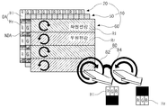
도 1은 종래의 편광안경 방식의 3차원 입체영상 표시장치의 사시도이다. FIG. 1 is a perspective view of a conventional three-dimensional stereoscopic image display apparatus using polarizing glasses.
도 1에 도시한 바와 같이, 편광안경 방식의 3차원 입체영상 표시장치(10)는, 영상을 표시하는 표시패널(20)과, 표시패널(20) 상부에 형성되는 편광필름(50)과, 편광필름(50) 상부에 형성되는 패턴드 리타더(patterned retarder)(60)를 포함한다.1, the polarizing glasses type three-dimensional
표시패널(20)은 영상을 표시하는 표시영역(DA)과 표시영역(DA) 사이의 비표시영역(NDA)을 포함하고, 표시영역(DA)은 좌안 수평화소라인(Hl) 및 우안 수평화소라인(Hr)을 포함한다.The
좌안영상을 표시하는 좌안 수평화소라인(Hl)과 우안영상을 표시하는 우안 수평화소라인(Hr)은 표시패널(20)의 수직방향을 따라 번갈아 배치되고, 좌안 수평화소라인(Hl) 및 우안 수평화소라인(Hr) 각각에는 적, 녹, 청색 화소영역(R, G, B)이 순차적으로 배치된다. The left eye horizontal pixel line Hl for displaying the left eye image and the right eye pixel line Hr for displaying the right eye image are alternately arranged along the vertical direction of the
편광필름(50)은, 표시패널(20)이 표시하는 좌안영상 및 우안영상을 각각 선편광된 좌안영상 및 선편광된 우안영상으로 변조하여 패턴드 리타더(60)에 전달한다. The polarizing
패턴드 리타더(60)는, 좌안 리타더(Rl) 및 우안 리타더(Rr)를 포함하는데, 좌안 리타더(Rl) 및 우안 리타더(Rr)는 각각 좌안 수평화소라인(Hl) 및 우안 수평화소라인(Hr)에 대응되어 표시패널(20)의 수직방향을 따라 번갈아 배치된다. The
여기서, 좌안 리타더(Rl)는 선편광을 좌원편광으로 변조하여 출력하고, 우안 리타더(Rr)는 선편광을 우원편광으로 변조하여 출력한다.Here, the left eye retarder Rl modulates the linearly polarized light into the left-handed circularly polarized light and outputs it, and the right-eye retarder Rr modulates the linearly polarized light into the right-handed circularly polarized light and outputs it.
따라서, 표시패널(20)의 좌안 수평화소라인(Hl)이 표시하는 좌안영상은, 편광필름(50)을 통과하면서 선편광 된 후, 패턴드 리타더(60)의 좌안 리타더(Rl)를 통과하면서 좌원편광 되고, 표시패널(20)의 우안 수평화소라인(Hr)이 표시하는 우안영상은, 편광필름(50)을 통과하면서 선편광 된 후, 패턴드 리타더(60)의 우안 리타더(Rr)를 통과하면서 우원편광 되어 시청자에게 전달된다. Therefore, the left eye image displayed by the left eye horizontal pixel line Hl of the
시청자가 착용하고 있는 편광안경(80)은, 좌안렌즈(82) 및 우안렌즈(84)를 포함하는데, 좌안렌즈(82)는 좌원편광만 투과시키고 우안렌즈(84)는 우원편광만 투과시킨다. The polarizing
따라서, 시청자에게 전달된 영상 중, 좌원편광 된 좌안영상은 좌안렌즈(82)를 통하여 시청자의 좌안에 전달되고, 우원편광 된 우안영상은 우안렌즈(84)를 통하여 시청자의 우안에 전달되며, 시청자는 좌우안으로 각각 전달된 좌안영상 및 우안영상을 조합하여 3차원 입체영상을 인식하게 된다.
Therefore, the left-handed circularly polarized left-eye image is transmitted to the viewer's left eye via the left-
그런데, 이러한 편광안경 방식의 3차원 입체영상 표시장치의 상하시야각 방향에서는, 주어진 단안 영상이 원치 않는 패턴드 리타더로 투과하여 좌안영상 및 우안영상이 시청자의 좌안 또는 우안에 동시에 전달되는 3차원 크로스토크(3D cross-talk)가 발생한다. 시야각이 커질수록 3차원 크로스토크가 증가하여 3차원 시야각(3D viewing angle)이 줄어들게 된다. In a direction of the upper and lower viewing angles of the polarizing glasses type three-dimensional stereoscopic image display apparatus, a given monocular image is transmitted through an undesired pattern reliader, and a left-eye image and a right-eye image are simultaneously transmitted to the viewer's left eye or right eye. Torque (3D cross-talk) occurs. As the viewing angle increases, the 3D crosstalk increases and the 3D viewing angle decreases.
따라서, 3차원 크로스토크를 방지하기 위해 패턴드 리타더에 블랙스트라이프(black stripe)를 형성하거나, 표시패널 내의 블랙매트릭스 폭을 증가시키는 방법이 제안되었다. Therefore, in order to prevent three-dimensional crosstalk, a method has been proposed in which a black stripe is formed in the pattern reliader, or the black matrix width in the display panel is increased.
이에 대해 도면을 참조하여 보다 상세히 설명한다. This will be described in more detail with reference to the drawings.
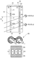
도 2a 내지 도 2c는 종래의 편광안경 방식의 3차원 입체영상 표시장치에 있어서, 3차원 크로스토크의 발생을 개략적으로 도시한 도면으로, 도 2a는 블랙스트라이프를 포함하지 않는 경우의 3차원 크로스토크를 도시한 도면이고, 도 2b는 블랙스트라이프를 포함하는 경우의 3차원 크로스토크를 도시한 도면이며, 도 2c는 블랙스트라이프 없이 블랙매트릭스의 폭을 증가시킨 경우의 3차원 크로스토크를 도시한 도면이다. FIGS. 2A to 2C are diagrams schematically showing generation of three-dimensional crosstalk in a conventional three-dimensional stereoscopic image display apparatus using polarizing glasses. FIG. 2A shows a three- FIG. 2B is a view showing a three-dimensional crosstalk when a black stripe is included, and FIG. 2C is a diagram showing a three-dimensional cross-talk when a width of a black matrix is increased without a black stripe .
도시하지는 않았지만, 도 2a 내지 도 2c의 편광안경 방식의 3차원 입체영상 표시장치의 정면 또는 좌우 시야각에서는, 표시패널(20)의 좌안 수평화소라인(Hl)이 표시하는 좌안영상(Il)이 패턴드 리타더(60)의 좌안 리타더(Rl)를 통과하여 좌원편광 되어 시청자에게 전달되고, 표시패널(20)의 우안 수평화소라인(Hr)이 표시하는 우안영상(Ir)이 패턴드 리타더(60)의 우안 리타더(Rr)를 통과하여 우원편광 되어 시청자에게 전달되므로, 좌안영상(Il) 및 우안영상(Ir)이 혼합되어 발생하는 3차원 크로스토크는 발생하지 않는다. Although not shown, the left eye image Il displayed by the left-eye horizontal pixel line Hl of the
하지만, 도 2a에 도시한 바와 같이, 편광안경 방식의 3차원 입체영상 표시장치의 상하 시야각에서는, 표시패널(20)의 좌안 수평화소라인(Hl)이 표시하는 좌안영상(Il)의 일부가 패턴드 리타더(60)의 우안 리타더(Rr)를 통과하여 우원편광 되어 출력된다. 2A, a part of the left-eye image Il displayed by the left-eye horizontal pixel line Hl of the
즉, 우안영상(Ir)과 일부의 좌안영상(Il)이 우원편광 되어 편광안경(80)의 우안렌즈(84)를 통과하여 시청자의 우안에 전달되므로, 우안영상(Ir)과 일부의 좌안영상(Il)이 서로 간섭하여 3차원 크로스토크가 발생하고, 상하방향의 3차원 시야각 특성이 저하된다. That is, since the right eye image Ir and a part of the left eye image Il are right circularly polarized and transmitted to the right eye of the viewer through the
물론, 표시패널(20)의 제1높이(h1)를 갖는 표시영역(DA) 사이에 배치된 비표시영역(NDA)에 의하여 좌안영상(Il) 및 우안영상(Ir)의 간섭을 저감할 수는 있지만, 표시패널(20)과 패턴드 리타더(60)가 비교적 멀리 떨어져 있으므로 3차원 크로스토크 방지 효과는 미미하다. Of course, the interference of the left eye image Il and the right eye image Ir can be reduced by the non-display area NDA disposed between the display areas DA having the first height h1 of the
이를 개선하기 위하여, 도 2b에 도시한 바와 같이, 패턴드 리타더(60)의 좌안 리타더(Rl) 및 우안 리타더(Rr) 사이에 블랙스트라이프(66)를 형성하거나, 도 2c에 도시한 바와 같이, 블랙스트라이프 없이 표시패널(20) 내부의 블랙매트릭스(43)의 폭을 증가시킬 수 있다. 2B, a
여기서, 표시패널(20)의 좌안 수평화소라인(Hl)이 표시하여 패턴드 리타더(60)의 우안 리타더(Rr)로 향하는 일부의 좌안영상(Il)은 블랙스트라이프(66) 또는 블랙매트릭스(43)에 의하여 차단되므로, 우원편광 되어 출력되지 않는다. Here, a part of the left eye image Il displayed by the left-eye horizontal pixel line Hl of the
즉, 우안영상(Ir)만이 우원편광 되어 편광안경(80)의 우안렌즈(84)를 통과하여 시청자의 우안에 전달되므로, 우안영상(Ir)과 일부의 좌안영상(Il)의 간섭에 의한 3차원 크로스토크가 방지되고, 상하방향의 3차원 시야각 특성이 개선된다. In other words, since only the right eye image Ir is right-polarized and passes through the
그러나, 표시패널(20)은, 도 2b에서와 같이 블랙스트라이프(66)에 의하여 비표시영역(NDA)보다 큰 블랙스트라이프영역(BS)을 포함하게 되어, 표시영역(DA)이 제1길이(h1)보다 작은 제2길이(h2)를 갖게 되거나, 또는, 도 2c에서와 같이 블랙매트릭스(43)에 의하여 비표시영역(NDA)이 증가하게 되어 표시영역(DA)이 제1길이(h1)보다 작은 제3길이(h3)를 갖게 되므로, 개구율이 줄어들어 휘도가 감소한다. However, the
백라이트 유닛의 휘도를 증가시켜 표시장치의 휘도를 향상시킬 수 있으나, 이를 위해 램프나 광학적 시트(optical sheet) 등의 부품이 추가되어야 하며, 이에 따라 제조 비용이 증가하게 된다. 또한, 램프 수의 증가로 전력소비가 증가하게 되고, 램프로부터의 발열량이 높아지게 되어 기기의 특성을 저하시키므로, 발열 문제 개선을 위한 방열 수단이 더 필요하게 된다.
The brightness of the display device can be improved by increasing the brightness of the backlight unit, but for this, components such as a lamp or an optical sheet must be added, thereby increasing the manufacturing cost. In addition, as the number of lamps increases, the power consumption increases, the amount of heat generated from the lamp increases, and the characteristics of the device deteriorate. Therefore, a heat dissipating means for improving the heat generation problem is further required.
본 발명은, 3차원 크로스토크를 방지하여 3차원 시야각 특성을 개선시킴과 동시에 개구율 및 휘도가 향상된 3차원 입체영상 표시장치 및 그 제조 방법을 제공하는데 그 목적이 있다.
It is an object of the present invention to provide a three-dimensional image display apparatus and a method of manufacturing the same that prevent three-dimensional crosstalk and improve three-dimensional viewing angle characteristics and improve aperture ratio and luminance.
상기의 목적을 달성하기 위하여, 본 발명의 영상 표시장치는, 제1기판 및 제2기판과, 상기 제1기판 및 제2기판 사이에 위치하며 좌안영상을 표시하는 좌안 수평화소라인 및 우안영상을 표시하는 우안 수평화소라인, 그리고 상기 좌안 수평화소라인과 우안 수평화소라인 사이의 블랙매트릭스를 포함하는 표시 패널과; 상기 제2기판 상부의 편광필름과; 상기 편광필름 상부에 위치하고, 상기 좌안 수평화소라인에 대응되는 좌안 리타더 및 상기 우안 수평화소라인에 대응되는 우안 리타더를 포함하는 패턴드 리타더; 그리고상기 패턴드 리타더 상부에 위치하는 보호기판을 포함하고, 상기 제2기판은 상기 제1기판 및 상기 보호기판보다 두께가 얇다.According to an aspect of the present invention, there is provided a video display device including a first substrate and a second substrate, a left-eye horizontal pixel line and a right-eye video line positioned between the first and second substrates, And a black matrix between the left-eye horizontal pixel line and the right-eye horizontal pixel line; A polarizing film on the second substrate; A pattern reliader positioned on the polarizing film and including a left eye retarder corresponding to the left eye horizontal pixel line and a right eye retarder corresponding to the right eye horizontal pixel line; And a protective substrate positioned above the pattern drift layer, wherein the second substrate is thinner than the first substrate and the protective substrate.
상기 제2기판과 상기 편광필름 사이에 블랙스트라이프를 더 포함한다.And a black stripe between the second substrate and the polarizing film.
상기 블랙스트라이프는 일정 단위로 서로 다른 폭을 가지는 패턴이 반복된다.The black stripes are repeated patterns having different widths in a predetermined unit.
상기 제1기판 내면에는 박막트랜지스터와, 상기 박막트랜지스터 상부에 위치하는 컬러필터층, 그리고 상기 박막트랜지스터에 연결된 화소 전극이 형성된다.On the inner surface of the first substrate, a thin film transistor, a color filter layer located above the thin film transistor, and a pixel electrode connected to the thin film transistor are formed.
본 발명의 영상 표시장치의 제조 방법은, 제1기판 및 제2기판과, 상기 제1기판 및 제2기판 사이에 위치하며 좌안영상을 표시하는 좌안 수평화소라인 및 우안영상을 표시하는 우안 수평화소라인, 그리고 상기 좌안 수평화소라인과 우안 수평화소라인 사이의 블랙매트릭스를 포함하는 표시 패널과; 상기 제2기판 상부의 편광필름과; 상기 편광필름 상부에 위치하고, 상기 좌안 수평화소라인에 대응되는 좌안 리타더 및 상기 우안 수평화소라인에 대응되는 우안 리타더를 포함하는 패턴드 리타더와; 상기 패턴드 리타더 상부에 위치하는 보호기판을 포함하는 영상 표시장치에 있어서, 상기 보호기판 상에 상기 패턴드 리타더를 형성 또는 부착하는 단계와; 상기 제2기판의 일면에 상기 편광필름을 부착하는 단계와; 상기 제2기판의 타면에 상기 블랙매트릭스를 형성하는 단계; 그리고 상기 보호기판 상에 형성된 패턴드 리타더와 상기 제2기판의 일면에 부착된 편광필름이 맞닿도록 합착하는 단계를 포함한다.A manufacturing method of a video display device of the present invention is a manufacturing method of a video display device including a first substrate and a second substrate, a left-eye horizontal pixel line positioned between the first and second substrates and displaying a left- Line, and a black matrix between the left-eye horizontal pixel line and the right-eye horizontal pixel line; A polarizing film on the second substrate; A patterned retarder positioned on the polarizing film and including a left eye retarder corresponding to the left eye horizontal pixel line and a right eye retarder corresponding to the right eye pixel line; And forming a pattern reliader on the protective substrate, the method comprising the steps of: forming or attaching the pattern reliader on the protective substrate; Attaching the polarizing film to one surface of the second substrate; Forming the black matrix on the other surface of the second substrate; And attaching the pattern reliader formed on the protective substrate to the polarizing film attached to one surface of the second substrate.
상기 제2기판의 타면에 상기 블랙매트릭스를 형성하는 단계는 상기 보호기판 상에 형성된 패턴드 리타더와 상기 제2기판의 일면에 부착된 편광필름이 맞닿도록 합착하는 단계 이후에 수행된다.The step of forming the black matrix on the other surface of the second substrate is performed after the step of attaching the pattern reliader formed on the protective substrate and the polarizing film attached to one surface of the second substrate to each other.
본 발명의 다른 영상 표시장치의 제조 방법은, 제1기판 및 제2기판과, 상기 제1기판 및 제2기판 사이에 위치하며 좌안영상을 표시하는 좌안 수평화소라인 및 우안영상을 표시하는 우안 수평화소라인, 그리고 상기 좌안 수평화소라인과 우안 수평화소라인 사이의 블랙매트릭스를 포함하는 표시 패널과; 상기 제2기판 상부의 편광필름과; 상기 편광필름 상부에 위치하고, 상기 좌안 수평화소라인에 대응되는 좌안 리타더 및 상기 우안 수평화소라인에 대응되는 우안 리타더를 포함하는 패턴드 리타더와; 상기 패턴드 리타더 상부에 위치하는 보호기판을 포함하는 영상 표시장치에 있어서, 상기 제2기판의 일면에 상기 편광필름을 부착하는 단계와; 상기 편광필름 상에 상기 패턴드 리타더를 형성 또는 부착하는 단계와; 상기 제2기판의 타면에 상기 블랙매트릭스를 형성하는 단계; 그리고 상기 편광필름을 사이에 두고 상기 제2기판의 일면에 위치하는 상기 패턴드 리타더를 상기 보호기판과 합착하는 단계를 포함한다.A method of manufacturing an image display apparatus according to another aspect of the present invention includes a first substrate and a second substrate, a left-eye horizontal pixel line positioned between the first and second substrates and displaying a left- Pixel lines, and a black matrix between the left-eye horizontal pixel line and the right-eye horizontal pixel line; A polarizing film on the second substrate; A patterned retarder positioned on the polarizing film and including a left eye retarder corresponding to the left eye horizontal pixel line and a right eye retarder corresponding to the right eye pixel line; The method comprising: attaching the polarizing film to one surface of the second substrate; Forming or attaching the pattern reliader on the polarizing film; Forming the black matrix on the other surface of the second substrate; And attaching the pattern reliader positioned on one surface of the second substrate to the protective substrate with the polarizing film therebetween.
상기 제2기판의 타면에 상기 블랙매트릭스를 형성하는 단계는 상기 편광필름을 사이에 두고 상기 제2기판의 일면에 위치하는 상기 패턴드 리타더를 상기 보호기판과 합착하는 단계 이후에 수행된다.The step of forming the black matrix on the other surface of the second substrate is performed after the step of attaching the pattern reliader positioned on one surface of the second substrate with the polarizing film interposed therebetween with the protective substrate.
본 발명의 다른 영상 표시장치의 제조 방법은, 제1기판 및 제2기판과, 상기 제1기판 및 제2기판 사이에 위치하며 좌안영상을 표시하는 좌안 수평화소라인 및 우안영상을 표시하는 우안 수평화소라인, 그리고 상기 좌안 수평화소라인과 우안 수평화소라인 사이의 블랙매트릭스를 포함하는 표시 패널과; 상기 제2기판 상부의 편광필름과; 상기 편광필름 상부에 위치하고, 상기 좌안 수평화소라인에 대응되는 좌안 리타더 및 상기 우안 수평화소라인에 대응되는 우안 리타더를 포함하는 패턴드 리타더와; 상기 패턴드 리타더 상부에 위치하는 보호기판을 포함하는 영상 표시장치에 있어서, 상기 편광필름과 상기 패턴드 리타더의 일체형을 준비하는 단계와; 상기 제2기판의 일면에 상기 편광필름이 위치하도록 일체형의 상기 편광필름과 상기 패턴드 리타더를 부착하는 단계와; 상기 제2기판의 타면에 상기 블랙매트릭스를 형성하는 단계; 그리고 상기 보호기판과 상기 패턴드 리타더가 맞닿도록 상기 제2기판의 일면에 부착된 일체형의 상기 편광필름과 상기 패턴드 리타더를 상기 보호기판과 합착하는 단계를 포함한다.A method of manufacturing an image display apparatus according to another aspect of the present invention includes a first substrate and a second substrate, a left-eye horizontal pixel line positioned between the first and second substrates and displaying a left- Pixel lines, and a black matrix between the left-eye horizontal pixel line and the right-eye horizontal pixel line; A polarizing film on the second substrate; A patterned retarder positioned on the polarizing film and including a left eye retarder corresponding to the left eye horizontal pixel line and a right eye retarder corresponding to the right eye pixel line; And a protective substrate disposed on the pattern reliader, the method comprising: preparing an integral type of the polarizing film and the pattern reliader; Attaching the patterned retarder and the polarizing film as one body so that the polarizing film is positioned on one side of the second substrate; Forming the black matrix on the other surface of the second substrate; And attaching the patterned retarder and the integral polarizing film attached to one surface of the second substrate such that the protective substrate and the patterned retarder abut each other with the protective substrate.
상기 제2기판의 타면에 상기 블랙매트릭스를 형성하는 단계는 상기 보호기판과 상기 패턴드 리타더가 맞닿도록 상기 제2기판의 일면에 부착된 일체형의 상기 편광필름과 상기 패턴드 리타더를 상기 보호기판과 합착하는 단계 이후에 수행된다.Wherein the step of forming the black matrix on the second surface of the second substrate includes the step of forming the polarizing film and the pattern reliader attached to one surface of the second substrate such that the protective substrate and the pattern reliader are in contact with each other, Is performed after the step of adhering to the substrate.
상기 제2기판은 상기 제1기판 및 상기 보호기판보다 두께가 얇다.The second substrate is thinner than the first substrate and the protective substrate.
본 발명은, 상기 제2기판과 상기 편광필름 사이에 블랙스트라이프를 형성하는 단계를 더 포함한다.The present invention further includes forming a black stripe between the second substrate and the polarizing film.
또한, 본 발명은, 상기 제1기판 상부에 박맥트랜지스터를 형성하는 단계와; 상기 박막트랜지스터 상부에 컬러필터층을 형성하는 단계; 그리고 상기 박막트랜지스터에 연결되는 화소 전극을 형성하는 단계를 더 포함한다.
According to another aspect of the present invention, there is provided a method of manufacturing a plasma display panel, Forming a color filter layer on the thin film transistor; And forming a pixel electrode connected to the thin film transistor.
본 발명에 따른 3차원 입체영상 표시장치에서는, 표시패널의 상부기판을 박형으로 하여 시야각을 개선하면서 블랙매트릭스의 폭을 줄여 개구율을 증가시키고 휘도를 향상시킬 수 있다. 이때, 이중 블랙스트라이프 구조를 적용하여 개구율을 더욱 증가시킬 수 있다.In the three-dimensional image display apparatus according to the present invention, the upper substrate of the display panel may be made thin to improve the viewing angle while reducing the width of the black matrix, thereby increasing the aperture ratio and improving the brightness. At this time, the aperture ratio can be further increased by applying a double black stripe structure.
휘도 개선에 따라, 램프나 광학적 시트 등의 부품을 생략할 수 있으므로, 비용을 낮출 수 있고, 램프 수의 감소로 전력소비가 감소하게 되고, 발열 문제가 개선되어 장치의 두께를 축소할 수 있다. As the luminance improves, parts such as lamps and optical sheets can be omitted. Therefore, the cost can be reduced, the power consumption can be reduced due to the reduction in the number of lamps, the heat generation problem can be improved, and the thickness of the device can be reduced.
한편, 보호기판을 적용함으로써, 박형기판 사용에 따른 내구성을 확보하여 기판 파손 및 패턴 왜곡을 방지할 수 있다.
On the other hand, by applying a protective substrate, it is possible to ensure durability as a result of using a thin substrate, thereby preventing substrate breakage and pattern distortion.
도 2a 내지 도 2c는 종래의 편광안경 방식의 3차원 입체영상 표시장치에 있어서, 3차원 크로스토크의 발생을 개략적으로 도시한 도면이다.
도 3은 본 발명의 실시예에 따른 3차원 입체영상 표시장치의 단면도이다.
도 4는 3차원 입체영상 표시장치에서 3차원 크로스토크를 계산하기 위한 개략적 도면이다.
도 5는 블랙매트릭스의 폭을 동일하게 하였을 때 제2기판 두께에 따른 3차원 시야각의 변화를 도시한 그래프이다.
도 6은 제2기판 두께에 따른 동일한 시야각을 얻을 수 있는 블랙매트릭스의 폭을 도시한 그래프이다.
도 7a 내지 도 7d는 본 발명의 제1실시예에 따른 3차원 입체영상 표시장치의 제조 공정을 도시한 단면도이다.
도 8a 내지 도 8d는 본 발명의 제1실시예에 따른 3차원 입체영상 표시장치의 제조 공정의 다른 예를 도시한 단면도이다.
도 9a 내지 도 9d는 본 발명의 제2실시예에 따른 3차원 입체영상 표시장치의 제조 공정을 도시한 단면도이다.
도 10a 내지 도 10d는 본 발명의 제2실시예에 따른 3차원 입체영상 표시장치의 제조 공정의 다른 예를 도시한 단면도이다.
도 11a 내지 도 11d는 본 발명의 제3실시예에 따른 3차원 입체영상 표시장치의 제조 공정을 도시한 단면도이다.
도 12a 내지 도 12d는 본 발명의 제3실시예에 따른 3차원 입체영상 표시장치의 제조 공정의 다른 예를 도시한 단면도이다.
도 13a는 본 발명의 실시예에 따른 3차원 입체영상 표시장치의 일례를 개략적으로 도시한 단면도이고, 도 13b는 본 발명의 실시예에 따른 3차원 입체영상 표시장치의 다른 예를 개략적으로 도시한 단면도이다.FIGS. 2A to 2C are diagrams schematically showing generation of three-dimensional crosstalk in a conventional three-dimensional stereoscopic image display apparatus using polarizing glasses. FIG.
3 is a cross-sectional view of a three-dimensional image display apparatus according to an exemplary embodiment of the present invention.
4 is a schematic diagram for calculating three-dimensional crosstalk in a three-dimensional image display apparatus.
5 is a graph showing a change in the three-dimensional viewing angle according to the thickness of the second substrate when the widths of the black matrix are made the same.
6 is a graph showing the width of a black matrix which can obtain the same viewing angle according to the second substrate thickness.
7A to 7D are cross-sectional views illustrating a manufacturing process of a three-dimensional image display apparatus according to a first embodiment of the present invention.
8A to 8D are cross-sectional views illustrating another example of a manufacturing process of the three-dimensional image display apparatus according to the first embodiment of the present invention.
9A to 9D are cross-sectional views illustrating a manufacturing process of a three-dimensional image display apparatus according to a second embodiment of the present invention.
10A to 10D are cross-sectional views illustrating another example of a manufacturing process of the three-dimensional image display device according to the second embodiment of the present invention.
11A to 11D are cross-sectional views illustrating a manufacturing process of a three-dimensional image display apparatus according to a third embodiment of the present invention.
12A to 12D are cross-sectional views illustrating another example of the manufacturing process of the three-dimensional image display apparatus according to the third embodiment of the present invention.
FIG. 13A is a cross-sectional view schematically showing an example of a three-dimensional image display apparatus according to an embodiment of the present invention, FIG. 13B is a view schematically showing another example of a three-dimensional image display apparatus according to an embodiment of the present invention Sectional view.
이하, 도면을 참조하여 본 발명의 실시예를 설명한다.Hereinafter, embodiments of the present invention will be described with reference to the drawings.
도 3은 본 발명의 실시예에 따른 3차원 입체영상 표시장치의 단면도이다. 3 is a cross-sectional view of a three-dimensional image display apparatus according to an exemplary embodiment of the present invention.
도 3에 도시한 바와 같이, 본 발명의 3차원 입체영상 표시장치는 표시패널(120)과, 상부 및 하부 편광판(150, 152)과, 패턴드 리타더(160) 및 보호기판(170)을 포함한다. 3, the three-dimensional image display apparatus of the present invention includes a
표시패널(120)에는 영상을 표시하는 표시영역(DA)과 표시영역(DA) 사이의 비표시영역(NDA)이 정의되고, 표시영역(DA)은 좌안 수평화소라인(Hl) 및 우안 수평화소라인(Hr)을 포함한다.A non-display area NDA between the display area DA for displaying an image and the display area DA is defined in the
표시패널(120)은, 서로 마주보며 이격된 제1 및 제2기판(122, 140)과, 제1 및 제2기판(122, 140) 사이에 형성된 액정층(148)을 포함한다. 제1 및 제2기판(122, 140)은 유리로 이루어진 기판일 수 있다.The
제1기판(122) 상부에는 게이트 배선(도시하지 않음)과 게이트 배선에 연결되는 게이트 전극(124)이 형성되고, 게이트 배선 및 게이트 전극(124) 상부에는 게이트 절연층(126)이 형성된다. A gate electrode 124 connected to a gate wiring (not shown) and a gate wiring is formed on the
게이트 전극(124)에 대응되는 게이트 절연층(126) 상부에는 반도체층(128)이 형성되고, 반도체층(128) 상부에는 서로 이격하는 소스 전극(132) 및 드레인 전극(134)과, 소스 전극(132)에 연결되는 데이터 배선(도시하지 않음)이 형성된다. 도시하지 않았지만, 반도체층(128)은 순수 비정질 실리콘으로 이루어진 액티브층과 불순물이 도핑된 비정질 실리콘으로 이루어진 오믹콘택층을 포함하며, 오믹콘택층은 소스 및 드레인 전극(132, 134)과 동일한 모양을 가질 수 있다. A semiconductor layer 128 is formed on the
데이터 배선은 게이트 배선과 교차하여 화소영역을 정의한다. The data wiring crosses the gate wiring to define the pixel region.
여기서, 게이트 전극(124), 반도체층(128), 소스 전극(132) 및 드레인 전극(134)은 박막트랜지스터(T)를 구성한다. Here, the gate electrode 124, the semiconductor layer 128, the
소스 전극(132), 드레인 전극(134) 및 데이터 배선 상부에는 보호층(136)이 형성되는데, 보호층(136)은 드레인 전극(134)을 노출하는 드레인 콘택홀(136a)을 포함한다. A
보호층(136) 상부에는 드레인 콘택홀(136a)을 통하여 드레인 전극(134)에 연결되는 화소 전극(138)이 화소영역 각각에 형성된다. A
제2기판(140) 하부에는 각 화소영역에 대응되는 개구부를 가지며 게이트 배선, 데이터 배선 및 박막트랜지스터(T)에 대응되는 블랙매트릭스(142)가 형성되고, 블랙매트릭스(142) 하부와 블랙매트릭스(142)의 개구부를 통하여 노출된 제2기판(140) 하부에는 컬러필터층(144)이 형성된다. 여기서, 블랙매트릭스(142)의 개구부는 표시 영역(DA)에 대응하며, 블랙매트릭스(142)는 비표시영역(NDA)에 대응한다.A
도시하지 않았지만, 컬러필터층(144)은 화소영역에 각각 대응되는 적, 녹, 청 컬러필터를 포함하며, 표시패널(120)을 정면에서 볼 때, 적, 녹, 청 컬러필터는 표시패널(120)의 수평방향을 따라 순차적으로 반복하여 배치되며, 표시패널(120)의 수직방향을 따라 동일 색의 컬러필터가 위치한다. Although not shown, the
그리고, 컬러필터층(144) 하부에는 투명한 공통 전극(146)이 형성된다. 여기서, 도시하지 않았지만, 컬러필터층(144)과 공통 전극(146) 사이에는 컬러필터층(144)의 보호 및 표면을 평탄화하기 위한 오버코트층이 더 형성될 수 있다.A transparent
액정층(148)은 제1기판(122)의 화소 전극(138)과 제2기판(140)의 공통 전극(146) 사이에 위치한다. 도시하지 않았지만, 액정층(148)과 화소 전극(138) 사이 및 액정층(148)과 공통 전극(146) 사이에는 액정 분자의 초기 배열을 결정하는 배향막이 각각 형성된다. The
여기서는 화소 전극(138)과 공통 전극(146)이 각각 제1 및 제2기판(122, 140)에 형성된 경우에 대하여 설명하였으나, 화소 전극(138)과 공통 전극(146)은 제1기판(122) 상에 모두 형성될 수 있다. 이때, 화소 전극(138)과 공통 전극(146)은 화소영역 내에서 패턴되어 서로 번갈아 배치될 수 있다. The
한편, 제1기판(122) 하부에는 하부편광판(152)이 위치하고, 제2기판(140) 상부에는 편광필름에 해당하는 상부편광판(150)이 위치한다. 상부 및 하부편광판(150, 152)은 광투과축에 평행한 선편광만을 투과시키며, 하부편광판(152)의 광투과축은 상부편광판(150)의 광투과축과 수직으로 배치된다. 제1기판(122)과 하부편광판(152) 사이 그리고 제2기판(140)과 상부편광판(150) 사이에는 점착층이 위치할 수 있다. The
도시하지 않았지만, 하부편광판(152) 아래에는 백라이트 유닛이 배치되어 표시패널(120)에 빛을 공급한다. Although not shown, a backlight unit is disposed below the
여기서는 표시패널(120)이 액정패널인 경우에 대하여 설명하였으나, 표시패널(120)은 유기전기발광패널일 수도 있다. 이때, 하부편광판(152)은 생략되며, 상부편광판(150)은 λ/4파장플레이트(quarter wave plate: QWP)와 선편광자(linear polarizer)로 구성될 수 있다. Here, the case where the
그리고, 상부편광판(150) 상부에는 패턴드 리타더(160)가 부착되는데, 패턴드 리타더(160)는, 표시패널(120)의 수직방향을 따라 번갈아 배치되는 좌안 리타더(Rl) 및 우안 리타더(Rr)를 포함한다. 좌안 리타더(R1)는 좌안 수평화소라인(Hl)에 대응하고, 우안 리타더(Rr)는 우안 수평화소라인(Hr)에 대응한다. The pattern reliader 160 is attached to the upper part of the
좌안 리타더(Rl) 및 우안 리타더(Rr)는, 사분의 일 파장(λ/4)만큼의 위상차를 발생시키는 사분파장판(quarter wave plate: QWP)으로, 그 광축을 표시패널 출사광인 선편광의 편광방향과 각각 +45도 및 -45도로 배치하여 구성할 수 있다. The left eye retarder Rl and the right eye retarder Rr are quarter wave plates (QWPs) that generate a phase difference by a quarter wavelength (? / 4), and their optical axes are linearly polarized light 45 degrees and -45 degrees, respectively, with respect to the polarization direction of the light.
패턴드 리타더(160) 상부에는 투명한 보호기판(170)이 위치한다. 보호기판(170)은 유리로 이루어질 수 있다. A transparent
따라서, 표시패널(120)의 좌안 수평화소라인(Hl)이 표시하는 좌안영상은, 상부편광판(150)을 통과하면서 선편광 된 후, 패턴드 리타더(160)의 좌안 리타더(Rl)를 통과하면서 좌원편광 되어 출사된다. 또한, 표시패널(120)의 우안 수평화소라인(Hr)이 표시하는 우안영상은, 상부편광판(150)을 통과하면서 선편광 된 후, 패턴드 리타더(160)의 우안 리타더(Rr)를 통과하면서 우원편광 되어 출사된다. Therefore, the left eye image displayed by the left-eye horizontal pixel line Hl of the
한편, 도시하지 않았지만, 시청자가 착용하고 있는 편광안경은, 좌안렌즈 및 우안렌즈를 포함하는데, 좌안렌즈는 좌원편광만 투과시키고 우안렌즈는 우원편광만 투과시킨다. On the other hand, although not shown, polarizing glasses worn by viewers include a left eye lens and a right eye lens, the left eye lens transmits only the left circularly polarized light, and the right eye lens transmits only right circularly polarized light.
따라서, 시청자에게 전달된 영상 중, 좌원편광 된 좌안영상은 좌안렌즈를 통하여 시청자의 좌안에 전달되고, 우원편광 된 우안영상은 우안렌즈를 통하여 시청자의 우안에 전달되며, 시청자는 좌우안으로 각각 전달된 좌안영상 및 우안영상을 조합하여 3차원 입체영상을 인식하게 된다. Therefore, the left-handed circularly polarized left-eye image is transmitted to the viewer's left eye through the left-eye lens, the right-handed circularly polarized right-eye image is transmitted to the viewer's right-eye through the right-eye lens, The left eye image and the right eye image are combined to recognize the three-dimensional image.
본 발명에서는 제2기판(140)의 두께를 얇게 하여 3차원 시야각을 개선시키며 개구율과 휘도를 향상시키며, 보호기판(170)을 통해 박형의 제2기판(140) 사용에 따른 불량을 최소화하는 것을 특징으로 한다. 이때, 제2기판(140)은 제1기판(122) 및 보호기판(170) 보다 얇은 두께를 가지며, 보호기판(170)은 제1기판(122)과 동일한 두께를 가지거나 얇은 두께를 가질 수 있다. In the present invention, the thickness of the
이에 대해 도 4를 참조하여 설명한다.This will be described with reference to FIG.
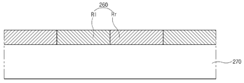
도 4는 3차원 입체영상 표시장치에서 3차원 크로스토크를 계산하기 위한 개략적 도면이다.4 is a schematic diagram for calculating three-dimensional crosstalk in a three-dimensional image display apparatus.
도 4에 도시한 바와 같이, 좌안 수평화소라인(Hl)과 우안 수평화소라인(Hr) 및 블랙매트릭스(182)를 포함하는 표시패널(180)과, 좌안 리타더(Rl)와 우안 리타더(Rr) 및 블랙스트라이프(192)를 포함하는 패턴드 리타더(190)가 일정 간격을 두고 배치된다. A
이때, 3차원 크로스토크가 발생하지 않는 출사각 θ는 다음의 식(1)로 표시될 수 있다.At this time, the outgoing angle? Where no three-dimensional crosstalk occurs can be expressed by the following equation (1).
tanθ = y/S = [{(W1+W2)/2}+(Pp-W1)×CT(0.07)×(1-Br)]/S --- 식(1)(1): tan? = y / S = {(W1 + W2) / 2} + (Pp-W1) CT (0.07)
여기서, S는 표시패널(180)과 패턴드 리타더(190) 사이의 거리이며, W1은 블랙매트릭스(182)의 폭이고, W2는 블랙스트라이프(192)의 폭이며, Pp는 표시패널(180)의 화소피치(pixel pitch)이고, CT(0.07)은 3차원 크로스토크가 7%인 것을 의미하며, Br은 블랙스트라이프(192)의 비율(ratio)이다. Where W is the width of the
따라서, S가 작아질수록 출사각 θ이 커져 3차원 시야각이 넓어지게 된다. Therefore, as S becomes smaller, the outgoing angle &thetas; becomes larger and the three-dimensional viewing angle becomes wider.
이때, S는 실질적으로 제2기판의 두께와 상부편광판의 두께, 접착제의 두께 및 패턴드 리타더(190)의 두께의 합에 해당하며, 제2기판의 두께를 줄임으로써 블랙매트릭스의 폭을 작게 하더라도 동일한 3차원 시야각을 얻을 수 있다. At this time, S corresponds to the sum of the thickness of the second substrate, the thickness of the upper polarizer, the thickness of the adhesive, and the thickness of the
도 5는 블랙매트릭스의 폭을 동일하게 하였을 때 제2기판 두께에 따른 3차원 시야각의 변화를 도시한 그래프이다. 5 is a graph showing a change in the three-dimensional viewing angle according to the thickness of the second substrate when the widths of the black matrix are made the same.
도 5에 도시한 바와 같이, 블랙매트릭스의 폭을 동일하게 하였을 때, 제2기판의 두께를 작게 할수록 3차원 시야각이 커지는 것을 알 수 있다.As shown in Fig. 5, when the width of the black matrix is made the same, the three-dimensional viewing angle increases as the thickness of the second substrate decreases.
한편, 도 6은 제2기판 두께에 따른 동일한 시야각을 얻을 수 있는 블랙매트릭스의 폭을 도시한 그래프로, 26도의 시야각을 기준으로 한다. Meanwhile, FIG. 6 is a graph showing the width of a black matrix that can obtain the same viewing angle according to the thickness of the second substrate, and is based on a viewing angle of 26 degrees.
도 6에 도시한 바와 같이, 제2기판의 두께를 작게 할 경우, 블랙매트릭스의 폭을 작게 하더라도 동일한 26도의 3차원 시야각을 얻을 수 있음을 알 수 있다. 일례로, 제2기판 두께가 약 0.2mm일 때, 제2기판 두께가 약 0.7mm인 경우의 블랙매트릭스 폭의 25%만 가지고도 동일한 3차원 시야각을 얻을 수 있다. As shown in Fig. 6, when the thickness of the second substrate is made small, it is understood that a similar three-dimensional viewing angle of 26 degrees can be obtained even if the width of the black matrix is made small. For example, when the thickness of the second substrate is about 0.2 mm, the same three-dimensional viewing angle can be obtained even if only 25% of the black matrix width in the case where the second substrate thickness is about 0.7 mm.
따라서, 제2기판의 두께를 작게 할 경우, 블랙매트릭스의 폭을 줄여 동일한 시야각을 얻을 수 있으며, 블랙매트릭스의 폭 감소에 따라 개구율 및 휘도를 향상시킬 수 있다.Therefore, when the thickness of the second substrate is reduced, the width of the black matrix can be reduced to obtain the same viewing angle, and the aperture ratio and brightness can be improved as the width of the black matrix decreases.
이러한 제2기판은 0 mm보다 크고 1.5 mm 보다 작은 두께를 가질 수 있으며, 바람직하게는 0.7 mm 이하의 두께를 가질 수 있다. Such a second substrate may have a thickness greater than 0 mm and less than 1.5 mm, and preferably less than 0.7 mm.
그런데, 제2기판의 두께가 얇아질 경우, 스트레스에 대한 내구성 저하로 블랙매트릭스나 컬러필터를 형성하는 공정 진행 중 기판이 파손되거나, 기판의 휨에 의한 패턴 왜곡과 같은 문제가 발생한다. However, when the thickness of the second substrate is reduced, the substrate is damaged during the process of forming the black matrix or the color filter due to the lowering of the durability against stress, and problems such as pattern distortion due to warping of the substrate occur.
이를 방지하기 위해, 본 발명에서는 보호기판을 사용하며, 공정순서를 변경하여 내구성을 증가시키고 불량을 막을 수 있다.In order to prevent this, a protective substrate is used in the present invention, and the durability and the defect can be prevented by changing the process sequence.
도 7a 내지 도 7d는 본 발명의 제1실시예에 따른 3차원 입체영상 표시장치의 제조 공정을 도시한 단면도로, 도 3의 표시장치에서 제1기판(122)과 그 상부에 형성된 구성 요소 및 하부편광판(152)을 제외한 구조이다. 7A to 7D are cross-sectional views illustrating a manufacturing process of the three-dimensional image display device according to the first embodiment of the present invention. In the display device of FIG. 3, a
도 7a에 도시한 바와 같이, 보호기판(270) 상에 패턴드 리타더(260)를 형성 또는 부착한다. 패턴드 리타더(260)는 번갈아 배치되는 좌안 리타더(Rl)와 우안 리타더(Rr)를 포함한다.As shown in FIG. 7A, the
보다 상세하게는, 보호기판(270) 상에 배향막(도시하지 않음)을 도포하고 경화한 후, 마스크를 통해 배향막에 편광된 자외선을 2회 조사하여 서로 다른 배향 방향을 갖는 영역을 형성한 다음, 배향막 상부에 액정 물질을 도포하고 경화함으로써, 서로 다른 방향으로 배열된 액정 물질로 이루어진 패턴드 리타더(260)를 형성한다. More specifically, after an alignment film (not shown) is applied and cured on the
또한, 도 7b에 도시한 바와 같이, 박형기판(240)의 일면에 편광필름(250)을 부착한다. 이때, 편광필름(250)과 박형기판(240) 사이에는 접착층(도시하지 않음)이 위치할 수 있다. Further, as shown in Fig. 7B, the
여기서, 도 7a와 도 7b의 순서는 서로 바뀔 수 있으며, 어느 것이 선행되어도 무방하다. Here, the order of Figs. 7A and 7B may be changed with each other, and any of them may be preceded.
다음, 도 7c에 도시한 바와 같이, 패턴드 리타더(260)가 형성된 보호기판(270)과 편광필름(250)이 부착된 박형기판(240)을 패턴드 리타더(260)와 편광필름(250)이 맞닿도록 합착한다. 이때, 편광필름(250)과 패턴드 리타더(260) 사이에는 접착층(도시하지 않음)이 위치할 수 있다.7C, the
이어, 도 7d에 도시한 바와 같이, 일면이 편광필름(250)과 패턴드 리타더(260)를 사이에 두고 보호기판(270)에 부착된 박형기판(240)의 타면에 블랙매트릭스(242)와 필요에 따라 컬러필터(244), 오버코트층이나 공통전극 등을 형성한다. 7D, a
따라서, 본 발명에서는 박형기판(240)을 사용하더라도 파손이나 패턴 왜곡과 같은 문제 없이 블랙매트릭스(242)나 컬러필터(244)를 형성할 수 있다. Therefore, even when the
한편, 편광필름(250)이 부착된 박형기판(240) 상에 블랙매트릭스(242)와 컬러필터(244)를 형성하고, 이어 편광필름(250)을 보호기판(270) 상에 형성된 패턴드 리타더(260)와 합착할 수도 있다. The
도 8a 내지 도 8d는 본 발명의 제1실시예에 따른 3차원 입체영상 표시장치의 제조 공정의 다른 예를 도시한 단면도이다. 8A to 8D are cross-sectional views illustrating another example of a manufacturing process of the three-dimensional image display apparatus according to the first embodiment of the present invention.
도 8a에 도시한 바와 같이, 보호기판(270) 상에 좌안 리타더(Rl)와 우안 리타더(Rr)를 포함하는 패턴드 리타더(260)를 형성 또는 부착한다. A
또한, 도 8b에 도시한 바와 같이, 박형기판(240)의 일면에 편광필름(250)을 부착한다. 이때, 편광필름(250)과 박형기판(240) 사이에는 접착층(도시하지 않음)이 위치할 수 있다. 8B, the
다음, 도 8c에 도시한 바와 같이, 박형기판(240)의 타면에 블랙매트릭스(242)를 형성하고, 필요에 따라 컬러필터(244), 오버코트층이나 공통전극 등을 형성한다. Next, as shown in FIG. 8C, a
이어, 도 8d에 도시한 바와 같이, 패턴드 리타더(260)가 형성된 보호기판(270)과 일면에 편광필름(250)이 부착되고 타면에 블랙매트릭스(242)와 컬러필터(244)가 형성된된 박형기판(240)을, 패턴드 리타더(260)와 편광필름(250)이 맞닿도록 합착한다. 이때, 편광필름(250)과 패턴드 리타더(260) 사이에는 접착층(도시하지 않음)이 위치할 수 있다.8D, a
도 9a 내지 도 9d는 본 발명의 제2실시예에 따른 3차원 입체영상 표시장치의 제조 공정을 도시한 단면도이다. 9A to 9D are cross-sectional views illustrating a manufacturing process of a three-dimensional image display apparatus according to a second embodiment of the present invention.
도 9a에 도시한 바와 같이, 박형기판(340)의 일면에 편광필름(350)을 부착한다. 이때, 편광필름(350)과 박형기판(340) 사이에는 접착층(도시하지 않음)이 위치할 수 있다. As shown in Fig. 9A, a
이어, 도 9b에 도시한 바와 같이, 박형기판(340)에 부착된 편광필름(350) 상에 좌안 리타더(Rl)와 우안 리타더(Rr)를 포함하는 패턴드 리타더(360)를 형성하거나 부착한다. 9B, a
다음, 도 9c에 도시한 바와 같이, 편광필름(350)을 사이에 두고 박형기판(340)의 일면에 위치하는 패턴드 리타더(360)를 보호기판(370)과 합착한다. 이때, 패턴드 리타더(360)와 보호기판(370) 사이에는 접착층(도시하지 않음)이 위치할 수 있다.Next, as shown in Fig. 9C, the
다음, 도 9d에 도시한 바와 같이, 편광필름(350) 및 패턴드 리타더(360)를 사이에 두고 보호기판(370)과 부착된 박형기판(340)의 타면에 블랙매트릭스(342)를 형성하고, 필요에 따라 컬러필터(344), 오버코트층이나 공통전극 등을 형성한다. Next, as shown in FIG. 9D, a
도 10a 내지 도 10d는 본 발명의 제2실시예에 따른 3차원 입체영상 표시장치의 제조 공정의 다른 예를 도시한 단면도이다. 10A to 10D are cross-sectional views illustrating another example of a manufacturing process of the three-dimensional image display device according to the second embodiment of the present invention.
도 10a에 도시한 바와 같이, 박형기판(340)의 일면에 편광필름(350)을 부착한다. 이때, 편광필름(350)과 박형기판(340) 사이에는 접착층(도시하지 않음)이 위치할 수 있다. 10A, a
이어, 도 10b에 도시한 바와 같이, 박형기판(340)에 부착된 편광필름(350) 상에 좌안 리타더(Rl)와 우안 리타더(Rr)를 포함하는 패턴드 리타더(360)를 형성하거나 부착한다. 10B, a
다음, 도 10c에 도시한 바와 같이, 일면에 편광필름(350)과 패턴드 리타더(360)가 순차적으로 위치하는 박형기판(340)의 타면에 블랙매트릭스(342)를 형성하고, 필요에 따라 컬러필터(344), 오버코트층이나 공통전극 등을 형성한다. Next, as shown in Fig. 10C, a
다음, 도 10d에 도시한 바와 같이, 편광필름(350)을 사이에 두고 박형기판(340)의 일면에 위치하는 패턴드 리타더(360)를 보호기판(370)과 합착한다. 이때, 패턴드 리타더(360)와 보호기판(370) 사이에는 접착층(도시하지 않음)이 위치할 수 있다.10D, the
도 11a 내지 도 11d는 본 발명의 제3실시예에 따른 3차원 입체영상 표시장치의 제조 공정을 도시한 단면도이다. 11A to 11D are cross-sectional views illustrating a manufacturing process of a three-dimensional image display apparatus according to a third embodiment of the present invention.
도 11a에 도시한 바와 같이, 편광필름(450)과 패턴드 리타더(460)가 일체형으로 공급되는 것을 준비한다. 패턴드 리타더(460)는 번갈아 위치하는 좌안 리타더(Rl)와 우안 리타더(Rr)를 포함한다.As shown in Fig. 11A, the
이어, 도 11b에 도시한 바와 같이, 일체형의 편광필름(450)과 패턴드 리타더(460)의 편광필름(450)을 박형기판(440)의 일면에 부착한다. 11B, an integral
다음, 도 11c에 도시한 바와 같이, 일면에 일체형의 편광필름(450)과 패턴드리타더(460)가 부착된 박형기판(440)의 타면에 블랙매트릭스(442)와 필요에 따라 컬러필터(444), 오버코트층이나 공통전극 등을 형성한다.Next, as shown in Fig. 11C, a
다음, 도 11d에 도시한 바와 같이, 박형기판(440)의 일면에 부착된 일체형의 편광필름(450)과 패턴드 리타더(460)를 보호기판(470)과 부착한다. 이때, 패턴드 리타더(460)와 보호기판(470) 사이에는 접착층(도시하지 않음)이 위치할 수 있다.11D, an integral
도 12a 내지 도 12d는 본 발명의 제3실시예에 따른 3차원 입체영상 표시장치의 제조 공정의 다른 예를 도시한 단면도이다. 12A to 12D are cross-sectional views illustrating another example of the manufacturing process of the three-dimensional image display apparatus according to the third embodiment of the present invention.
도 12a에 도시한 바와 같이, 편광필름(450)과 패턴드 리타더(460)가 일체형으로 공급되는 것을 준비한다. 패턴드 리타더(460)는 번갈아 위치하는 좌안 리타더(Rl)와 우안 리타더(Rr)를 포함한다.As shown in Fig. 12A, the
이어, 도 12b에 도시한 바와 같이, 일체형의 편광필름(450)과 패턴드 리타더(460)의 편광필름(450)을 박형기판(440)의 일면에 부착한다. 12B, a monolithic
다음, 도 12c에 도시한 바와 같이, 박형기판(440)의 일면에 부착된 일체형의 편광필름(450)과 패턴드 리타더(460)의 패턴드 리타더(460)를 보호기판(470)과 부착한다. 이때, 패턴드 리타더(460)와 보호기판(470) 사이에는 접착층(도시하지 않음)이 위치할 수 있다.12C, the integral
다음, 도 12d에 도시한 바와 같이, 일면이 일체형의 편광필름(450)과 패턴드리타더(460)를 사이에 두고 보호기판(470)에 부착된 박형기판(440)의 타면에 블랙매트릭스(442)를 형성하고, 필요에 따라 컬러필터(444), 오버코트층이나 공통전극 등을 형성한다.Next, as shown in Fig. 12D, a
이와 같이, 본 발명에서는 박형기판을 사용하여 시야각을 증가시키며 개구율 및 휘도를 향상시키는데 있어서, 박형기판에 편광필름과 패턴드 리타더 및 보호기판을 선택적으로 부착하여 내구성을 증가시킴으로써, 공정 진행 중 기판의 파손이나 기판이 휘어 나타나는 패턴 왜곡을 방지할 수 있다. As described above, in the present invention, in order to increase the viewing angle and improve the aperture ratio and the brightness by using the thin substrate, the polarizing film, the pattern reliader and the protective substrate are selectively attached to the thin substrate to increase the durability, It is possible to prevent the breakage of the substrate or the distortion of the pattern in which the substrate is warped.
여기서, 컬러필터를 박막트랜지스터와 같은 기판 상에 형성하는 컬러필터 온 박막트랜지스터(color filter on TFT) 구조나 박막트랜지스터 온 컬러필터(TFT on color filter) 구조에 적용 할 경우, 박형기판에 진행되는 공정수가 최소화될 수 있으므로, 파손을 더욱 방지하고 패턴드 리타더에 가해지는 부작용을 더욱 줄일 수 있다.
Here, when applied to a color filter on TFT structure or a TFT on color filter structure in which a color filter is formed on a substrate such as a thin film transistor, The number can be minimized, so that it is possible to further prevent breakage and to further reduce the adverse effects on the patterned retarder.
한편, 블랙스트라이프(black stripe)를 더 포함하는 이중 블랙스트라이프(double black stripe) 구조를 적용하여 보다 넓은 개구율을 확보할 수 있다.On the other hand, a wide aperture ratio can be secured by applying a double black stripe structure including a black stripe.
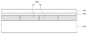
도 13a는 본 발명의 실시예에 따른 3차원 입체영상 표시장치의 일례를 개략적으로 도시한 단면도이고, 도 13b는 본 발명의 실시예에 따른 3차원 입체영상 표시장치의 다른 예를 개략적으로 도시한 단면도로, 도 13a는 블랙매트릭스를 포함하고, 도 13b는 블랙매트릭스와 블랙스트라이프를 포함한다. FIG. 13A is a cross-sectional view schematically showing an example of a three-dimensional image display apparatus according to an embodiment of the present invention, FIG. 13B is a view schematically showing another example of a three-dimensional image display apparatus according to an embodiment of the present invention In the sectional view, Fig. 13A includes a black matrix, and Fig. 13B includes a black matrix and a black stripe.
도 13a와 도 13b에 도시한 바와 같이, 표시패널(520)의 제1기판(522)과 제2기판(540) 사이에는 좌안 수평화소라인(Hl)과 우안 수평화소라인(Hr)이 번갈아 위치하고, 좌안 수평화소라인(Hl)과 우안 수평화소라인(Hr) 사이에는 블랙매트릭스(542)가 위치한다. As shown in FIGS. 13A and 13B, a left-eye horizontal pixel line Hl and a right-eye horizontal pixel line Hr are alternately disposed between the
제2기판(540)의 바깥쪽 면에는 편광필름(550)과, 좌안 리타더(Rl) 및 우안 리타더(Rr)를 포함하는 패턴드 리타더(560), 그리고 보호기판(570)이 차례로 위치한다. A
이때, 도 13b에 도시한 바와 같이, 본 발명의 실시예에 따른 3차원 입체영상 표시장치의 다른 예에서는, 제2기판(540)과 편광필름(550) 사이에 블랙스트라이프(555)가 위치한다. 13B, in another example of the three-dimensional image display apparatus according to the embodiment of the present invention, a
여기서, 도 13b의 블랙매트릭스(542)의 폭(w12)을 도 13a의 블랙매트릭스(542)는 폭(w11) 보다 작게 하더라도, 동일한 출사각 θ1을 얻을 수 있다. 도 13b의 경우, 블랙매트릭스(542)의 폭(w12)을 작게 하더라도, 블랙스트라이프(555)에 의해 주어진 단안 영상이 원치 않는 패턴드 리타더로 투과되는 것이 차단된다. 따라서, 블랙매트릭스(542)의 폭(w12)을 작게 하여 개구율을 더욱 높일 수 있다. Here, even if the width w12 of the
이러한 블랙스트라이프(555)는 블랙매트릭스(542)와 다른 피치를 가질 수 있으며, 블랙매트릭스(542)와 중첩되지 않고 어긋나게 배치될 수 있다. The
또한, 블랙스트라이프(555)의 폭을 동일하게 하지 않고 일정 단위로 서로 다른 폭을 반복함으로써, 휘도 균일도를 향상시킬 수도 있다. 일례로, 블랙스트라이프(555)의 폭을 각각 20㎛, 25㎛, 30㎛, 25㎛, 20㎛으로 하고, 이러한 폭을 반복할 수 있다.
In addition, it is also possible to improve the luminance uniformity by repeating different widths in a predetermined unit without making the width of the
한편, 본 발명의 실시예에서는 패턴드 리타더가 사분의 일 파장(λ/4)만큼의 위상차를 발생시키는 사분파장판(quarter wave plate: QWP)인 경우를 예로 하였으나, 패턴드 리타더는 반 파장(λ/2)만큼의 위상차를 발생시키는 반파장판(half wave plate: HWP)일 수 있다. 이때, 편광안경의 좌안렌즈 및 우안렌즈 또한 반파장판을 포함하는 것이 바람직하다.
Meanwhile, in the embodiment of the present invention, the case where the pattern reliader is a quarter wave plate (QWP) generating a phase difference by a quarter wavelength (? / 4) is exemplified, And may be a half wave plate (HWP) that generates a phase difference by a wavelength (? / 2). At this time, it is preferable that the left eye lens and the right eye lens of the polarizing glasses also include half wave plates.
본 발명은 상기한 실시예에 한정되지 아니하며, 본 발명의 정신을 벗어나지 않는 이상 다양한 변화와 변형이 가능하다.
The present invention is not limited to the above-described embodiments, and various changes and modifications may be made without departing from the spirit of the present invention.
이하, 도면을 참조하여 본 발명의 실시예를 설명한다.
도 3은 본 발명의 실시예에 따른 3차원 입체영상 표시장치의 단면도이다.
도 3에 도시한 바와 같이, 본 발명의 3차원 입체영상 표시장치는 표시패널(120)과, 상부 및 하부 편광판(150, 152)과, 패턴드 리타더(160) 및 보호기판(170)을 포함한다.
표시패널(120)에는 영상을 표시하는 표시영역(DA)과 표시영역(DA) 사이의 비표시영역(NDA)이 정의되고, 표시영역(DA)은 좌안 수평화소라인(Hl) 및 우안 수평화소라인(Hr)을 포함한다.
표시패널(120)은, 서로 마주보며 이격된 제1 및 제2기판(122, 140)과, 제1 및 제2기판(122, 140) 사이에 형성된 액정층(148)을 포함한다. 제1 및 제2기판(122, 140)은 유리로 이루어진 기판일 수 있다.
제1기판(122) 상부에는 게이트 배선(도시하지 않음)과 게이트 배선에 연결되는 게이트 전극(124)이 형성되고, 게이트 배선 및 게이트 전극(124) 상부에는 게이트 절연층(126)이 형성된다.
게이트 전극(124)에 대응되는 게이트 절연층(126) 상부에는 반도체층(128)이 형성되고, 반도체층(128) 상부에는 서로 이격하는 소스 전극(132) 및 드레인 전극(134)과, 소스 전극(132)에 연결되는 데이터 배선(도시하지 않음)이 형성된다. 도시하지 않았지만, 반도체층(128)은 순수 비정질 실리콘으로 이루어진 액티브층과 불순물이 도핑된 비정질 실리콘으로 이루어진 오믹콘택층을 포함하며, 오믹콘택층은 소스 및 드레인 전극(132, 134)과 동일한 모양을 가질 수 있다.
데이터 배선은 게이트 배선과 교차하여 화소영역을 정의한다.
여기서, 게이트 전극(124), 반도체층(128), 소스 전극(132) 및 드레인 전극(134)은 박막트랜지스터(T)를 구성한다.
소스 전극(132), 드레인 전극(134) 및 데이터 배선 상부에는 보호층(136)이 형성되는데, 보호층(136)은 드레인 전극(134)을 노출하는 드레인 콘택홀(136a)을 포함한다.
보호층(136) 상부에는 드레인 콘택홀(136a)을 통하여 드레인 전극(134)에 연결되는 화소 전극(138)이 화소영역 각각에 형성된다.
제2기판(140) 하부에는 각 화소영역에 대응되는 개구부를 가지며 게이트 배선, 데이터 배선 및 박막트랜지스터(T)에 대응되는 블랙매트릭스(142)가 형성되고, 블랙매트릭스(142) 하부와 블랙매트릭스(142)의 개구부를 통하여 노출된 제2기판(140) 하부에는 컬러필터층(144)이 형성된다. 여기서, 블랙매트릭스(142)의 개구부는 표시 영역(DA)에 대응하며, 블랙매트릭스(142)는 비표시영역(NDA)에 대응한다.
도시하지 않았지만, 컬러필터층(144)은 화소영역에 각각 대응되는 적, 녹, 청 컬러필터를 포함하며, 표시패널(120)을 정면에서 볼 때, 적, 녹, 청 컬러필터는 표시패널(120)의 수평방향을 따라 순차적으로 반복하여 배치되며, 표시패널(120)의 수직방향을 따라 동일 색의 컬러필터가 위치한다.
그리고, 컬러필터층(144) 하부에는 투명한 공통 전극(146)이 형성된다. 여기서, 도시하지 않았지만, 컬러필터층(144)과 공통 전극(146) 사이에는 컬러필터층(144)의 보호 및 표면을 평탄화하기 위한 오버코트층이 더 형성될 수 있다.
액정층(148)은 제1기판(122)의 화소 전극(138)과 제2기판(140)의 공통 전극(146) 사이에 위치한다. 도시하지 않았지만, 액정층(148)과 화소 전극(138) 사이 및 액정층(148)과 공통 전극(146) 사이에는 액정 분자의 초기 배열을 결정하는 배향막이 각각 형성된다.
여기서는 화소 전극(138)과 공통 전극(146)이 각각 제1 및 제2기판(122, 140)에 형성된 경우에 대하여 설명하였으나, 화소 전극(138)과 공통 전극(146)은 제1기판(122) 상에 모두 형성될 수 있다. 이때, 화소 전극(138)과 공통 전극(146)은 화소영역 내에서 패턴되어 서로 번갈아 배치될 수 있다.
한편, 제1기판(122) 하부에는 하부편광판(152)이 위치하고, 제2기판(140) 상부에는 편광필름에 해당하는 상부편광판(150)이 위치한다. 상부 및 하부편광판(150, 152)은 광투과축에 평행한 선편광만을 투과시키며, 하부편광판(152)의 광투과축은 상부편광판(150)의 광투과축과 수직으로 배치된다. 제1기판(122)과 하부편광판(152) 사이 그리고 제2기판(140)과 상부편광판(150) 사이에는 점착층이 위치할 수 있다.
도시하지 않았지만, 하부편광판(152) 아래에는 백라이트 유닛이 배치되어 표시패널(120)에 빛을 공급한다.
여기서는 표시패널(120)이 액정패널인 경우에 대하여 설명하였으나, 표시패널(120)은 유기전기발광패널일 수도 있다. 이때, 하부편광판(152)은 생략되며, 상부편광판(150)은 λ/4파장플레이트(quarter wave plate: QWP)와 선편광자(linear polarizer)로 구성될 수 있다.
그리고, 상부편광판(150) 상부에는 패턴드 리타더(160)가 부착되는데, 패턴드 리타더(160)는, 표시패널(120)의 수직방향을 따라 번갈아 배치되는 좌안 리타더(Rl) 및 우안 리타더(Rr)를 포함한다. 좌안 리타더(R1)는 좌안 수평화소라인(Hl)에 대응하고, 우안 리타더(Rr)는 우안 수평화소라인(Hr)에 대응한다.
좌안 리타더(Rl) 및 우안 리타더(Rr)는, 사분의 일 파장(λ/4)만큼의 위상차를 발생시키는 사분파장판(quarter wave plate: QWP)으로, 그 광축을 표시패널 출사광인 선편광의 편광방향과 각각 +45도 및 -45도로 배치하여 구성할 수 있다.
패턴드 리타더(160) 상부에는 투명한 보호기판(170)이 위치한다. 보호기판(170)은 유리로 이루어질 수 있다.
따라서, 표시패널(120)의 좌안 수평화소라인(Hl)이 표시하는 좌안영상은, 상부편광판(150)을 통과하면서 선편광 된 후, 패턴드 리타더(160)의 좌안 리타더(Rl)를 통과하면서 좌원편광 되어 출사된다. 또한, 표시패널(120)의 우안 수평화소라인(Hr)이 표시하는 우안영상은, 상부편광판(150)을 통과하면서 선편광 된 후, 패턴드 리타더(160)의 우안 리타더(Rr)를 통과하면서 우원편광 되어 출사된다.
한편, 도시하지 않았지만, 시청자가 착용하고 있는 편광안경은, 좌안렌즈 및 우안렌즈를 포함하는데, 좌안렌즈는 좌원편광만 투과시키고 우안렌즈는 우원편광만 투과시킨다.
따라서, 시청자에게 전달된 영상 중, 좌원편광 된 좌안영상은 좌안렌즈를 통하여 시청자의 좌안에 전달되고, 우원편광 된 우안영상은 우안렌즈를 통하여 시청자의 우안에 전달되며, 시청자는 좌우안으로 각각 전달된 좌안영상 및 우안영상을 조합하여 3차원 입체영상을 인식하게 된다.
본 발명에서는 제2기판(140)의 두께를 얇게 하여 3차원 시야각을 개선시키며 개구율과 휘도를 향상시키며, 보호기판(170)을 통해 박형의 제2기판(140) 사용에 따른 불량을 최소화하는 것을 특징으로 한다. 이때, 제2기판(140)은 제1기판(122) 및 보호기판(170) 보다 얇은 두께를 가지며, 보호기판(170)은 제1기판(122)과 동일한 두께를 가지거나 얇은 두께를 가질 수 있다.
이에 대해 도 4를 참조하여 설명한다.
도 4는 3차원 입체영상 표시장치에서 3차원 크로스토크를 계산하기 위한 개략적 도면이다.
도 4에 도시한 바와 같이, 좌안 수평화소라인(Hl)과 우안 수평화소라인(Hr) 및 블랙매트릭스(182)를 포함하는 표시패널(180)과, 좌안 리타더(Rl)와 우안 리타더(Rr) 및 블랙스트라이프(192)를 포함하는 패턴드 리타더(190)가 일정 간격을 두고 배치된다.
이때, 3차원 크로스토크가 발생하지 않는 출사각 θ는 다음의 식(1)로 표시될 수 있다.
tanθ = y/S = [{(W1+W2)/2}+(Pp-W1)×CT(0.07)X(1-Br)]/S --- 식(1)
여기서, S는 표시패널(180)과 패턴드 리타더(190) 사이의 거리이며, W1은 블랙매트릭스(182)의 폭이고, W2는 블랙스트라이프(192)의 폭이며, Pp는 표시패널(180)의 화소피치(pixel pitch)이고, CT(0.07)은 3차원 크로스토크가 7%인 것을 의미하며, Br은 블랙스트라이프(192)의 비율(ratio)이다.
따라서, S가 작아질수록 출사각 θ이 커져 3차원 시야각이 넓어지게 된다.
이때, S는 실질적으로 제2기판의 두께와 상부편광판의 두께, 접착제의 두께 및 패턴드 리타더(190)의 두께의 합에 해당하며, 제2기판의 두께를 줄임으로써 블랙매트릭스의 폭을 작게 하더라도 동일한 3차원 시야각을 얻을 수 있다.
도 5는 블랙매트릭스의 폭을 동일하게 하였을 때 제2기판 두께에 따른 3차원 시야각의 변화를 도시한 그래프이다.
도 5에 도시한 바와 같이, 블랙매트릭스의 폭을 동일하게 하였을 때, 제2기판의 두께를 작게 할수록 3차원 시야각이 커지는 것을 알 수 있다.
한편, 도 6은 제2기판 두께에 따른 동일한 시야각을 얻을 수 있는 블랙매트릭스의 폭을 도시한 그래프로, 26도의 시야각을 기준으로 한다.
도 6에 도시한 바와 같이, 제2기판의 두께를 작게 할 경우, 블랙매트릭스의 폭을 작게 하더라도 동일한 26도의 3차원 시야각을 얻을 수 있음을 알 수 있다. 일례로, 제2기판 두께가 약 0.2mm일 때, 제2기판 두께가 약 0.7mm인 경우의 블랙매트릭스 폭의 25%만 가지고도 동일한 3차원 시야각을 얻을 수 있다.
따라서, 제2기판의 두께를 작게 할 경우, 블랙매트릭스의 폭을 줄여 동일한 시야각을 얻을 수 있으며, 블랙매트릭스의 폭 감소에 따라 개구율 및 휘도를 향상시킬 수 있다.
이러한 제2기판은 0 mm보다 크고 1.5 mm 보다 작은 두께를 가질 수 있으며, 바람직하게는 0.7 mm 이하의 두께를 가질 수 있다.
그런데, 제2기판의 두께가 얇아질 경우, 스트레스에 대한 내구성 저하로 블랙매트릭스나 컬러필터를 형성하는 공정 진행 중 기판이 파손되거나, 기판의 휨에 의한 패턴 왜곡과 같은 문제가 발생한다.
이를 방지하기 위해, 본 발명에서는 보호기판을 사용하며, 공정순서를 변경하여 내구성을 증가시키고 불량을 막을 수 있다.
도 7a 내지 도 7d는 본 발명의 제1실시예에 따른 3차원 입체영상 표시장치의 제조 공정을 도시한 단면도로, 도 3의 표시장치에서 제1기판(122)과 그 상부에 형성된 구성 요소 및 하부편광판(152)을 제외한 구조이다.
도 7a에 도시한 바와 같이, 보호기판(270) 상에 패턴드 리타더(260)를 형성 또는 부착한다. 패턴드 리타더(260)는 번갈아 배치되는 좌안 리타더(Rl)와 우안 리타더(Rr)를 포함한다.
보다 상세하게는, 보호기판(270) 상에 배향막(도시하지 않음)을 도포하고 경화한 후, 마스크를 통해 배향막에 편광된 자외선을 2회 조사하여 서로 다른 배향 방향을 갖는 영역을 형성한 다음, 배향막 상부에 액정 물질을 도포하고 경화함으로써, 서로 다른 방향으로 배열된 액정 물질로 이루어진 패턴드 리타더(260)를 형성한다.
또한, 도 7b에 도시한 바와 같이, 박형기판(240)의 일면에 편광필름(250)을 부착한다. 이때, 편광필름(250)과 박형기판(240) 사이에는 접착층(도시하지 않음)이 위치할 수 있다.
여기서, 도 7a와 도 7b의 순서는 서로 바뀔 수 있으며, 어느 것이 선행되어도 무방하다.
다음, 도 7c에 도시한 바와 같이, 패턴드 리타더(260)가 형성된 보호기판(270)과 편광필름(250)이 부착된 박형기판(240)을 패턴드 리타더(260)와 편광필름(250)이 맞닿도록 합착한다. 이때, 편광필름(250)과 패턴드 리타더(260) 사이에는 접착층(도시하지 않음)이 위치할 수 있다.
이어, 도 7d에 도시한 바와 같이, 일면이 편광필름(250)과 패턴드 리타더(260)를 사이에 두고 보호기판(270)에 부착된 박형기판(240)의 타면에 블랙매트릭스(242)와 필요에 따라 컬러필터(244), 오버코트층이나 공통전극 등을 형성한다.
따라서, 본 발명에서는 박형기판(240)을 사용하더라도 파손이나 패턴 왜곡과 같은 문제 없이 블랙매트릭스(242)나 컬러필터(244)를 형성할 수 있다.
한편, 편광필름(250)이 부착된 박형기판(240) 상에 블랙매트릭스(242)와 컬러필터(244)를 형성하고, 이어 편광필름(250)을 보호기판(270) 상에 형성된 패턴드 리타더(260)와 합착할 수도 있다.
도 8a 내지 도 8d는 본 발명의 제1실시예에 따른 3차원 입체영상 표시장치의 제조 공정의 다른 예를 도시한 단면도이다.
도 8a에 도시한 바와 같이, 보호기판(270) 상에 좌안 리타더(Rl)와 우안 리타더(Rr)를 포함하는 패턴드 리타더(260)를 형성 또는 부착한다.
또한, 도 8b에 도시한 바와 같이, 박형기판(240)의 일면에 편광필름(250)을 부착한다. 이때, 편광필름(250)과 박형기판(240) 사이에는 접착층(도시하지 않음)이 위치할 수 있다.
다음, 도 8c에 도시한 바와 같이, 박형기판(240)의 타면에 블랙매트릭스(242)를 형성하고, 필요에 따라 컬러필터(244), 오버코트층이나 공통전극 등을 형성한다.
이어, 도 8d에 도시한 바와 같이, 패턴드 리타더(260)가 형성된 보호기판(270)과 일면에 편광필름(250)이 부착되고 타면에 블랙매트릭스(242)와 컬러필터(244)가 형성된된 박형기판(240)을, 패턴드 리타더(260)와 편광필름(250)이 맞닿도록 합착한다. 이때, 편광필름(250)과 패턴드 리타더(260) 사이에는 접착층(도시하지 않음)이 위치할 수 있다.
도 9a 내지 도 9d는 본 발명의 제2실시예에 따른 3차원 입체영상 표시장치의 제조 공정을 도시한 단면도이다.
도 9a에 도시한 바와 같이, 박형기판(340)의 일면에 편광필름(350)을 부착한다. 이때, 편광필름(350)과 박형기판(340) 사이에는 접착층(도시하지 않음)이 위치할 수 있다.
이어, 도 9b에 도시한 바와 같이, 박형기판(340)에 부착된 편광필름(350) 상에 좌안 리타더(Rl)와 우안 리타더(Rr)를 포함하는 패턴드 리타더(360)를 형성하거나 부착한다.
다음, 도 9c에 도시한 바와 같이, 편광필름(350)을 사이에 두고 박형기판(340)의 일면에 위치하는 패턴드 리타더(360)를 보호기판(370)과 합착한다. 이때, 패턴드 리타더(360)와 보호기판(370) 사이에는 접착층(도시하지 않음)이 위치할 수 있다.
다음, 도 9d에 도시한 바와 같이, 편광필름(350) 및 패턴드 리타더(360)를 사이에 두고 보호기판(370)과 부착된 박형기판(340)의 타면에 블랙매트릭스(342)를 형성하고, 필요에 따라 컬러필터(344), 오버코트층이나 공통전극 등을 형성한다.
도 10a 내지 도 10d는 본 발명의 제2실시예에 따른 3차원 입체영상 표시장치의 제조 공정의 다른 예를 도시한 단면도이다.
도 10a에 도시한 바와 같이, 박형기판(340)의 일면에 편광필름(350)을 부착한다. 이때, 편광필름(350)과 박형기판(340) 사이에는 접착층(도시하지 않음)이 위치할 수 있다.
이어, 도 10b에 도시한 바와 같이, 박형기판(340)에 부착된 편광필름(350) 상에 좌안 리타더(Rl)와 우안 리타더(Rr)를 포함하는 패턴드 리타더(360)를 형성하거나 부착한다.
다음, 도 10c에 도시한 바와 같이, 일면에 편광필름(350)과 패턴드 리타더(360)가 순차적으로 위치하는 박형기판(340)의 타면에 블랙매트릭스(342)를 형성하고, 필요에 따라 컬러필터(344), 오버코트층이나 공통전극 등을 형성한다.
다음, 도 10d에 도시한 바와 같이, 편광필름(350)을 사이에 두고 박형기판(340)의 일면에 위치하는 패턴드 리타더(360)를 보호기판(370)과 합착한다. 이때, 패턴드 리타더(360)와 보호기판(370) 사이에는 접착층(도시하지 않음)이 위치할 수 있다.
도 11a 내지 도 11d는 본 발명의 제3실시예에 따른 3차원 입체영상 표시장치의 제조 공정을 도시한 단면도이다.
도 11a에 도시한 바와 같이, 편광필름(450)과 패턴드 리타더(460)가 일체형으로 공급되는 것을 준비한다. 패턴드 리타더(460)는 번갈아 위치하는 좌안 리타더(Rl)와 우안 리타더(Rr)를 포함한다.
이어, 도 11b에 도시한 바와 같이, 일체형의 편광필름(450)과 패턴드 리타더(460)의 편광필름(450)을 박형기판(440)의 일면에 부착한다.
다음, 도 11c에 도시한 바와 같이, 일면에 일체형의 편광필름(450)과 패턴드리타더(460)가 부착된 박형기판(440)의 타면에 블랙매트릭스(442)와 필요에 따라 컬러필터(444), 오버코트층이나 공통전극 등을 형성한다.
다음, 도 11d에 도시한 바와 같이, 박형기판(440)의 일면에 부착된 일체형의 편광필름(450)과 패턴드 리타더(460)를 보호기판(470)과 부착한다. 이때, 패턴드 리타더(460)와 보호기판(470) 사이에는 접착층(도시하지 않음)이 위치할 수 있다.
도 12a 내지 도 12d는 본 발명의 제3실시예에 따른 3차원 입체영상 표시장치의 제조 공정의 다른 예를 도시한 단면도이다.
도 12a에 도시한 바와 같이, 편광필름(450)과 패턴드 리타더(460)가 일체형으로 공급되는 것을 준비한다. 패턴드 리타더(460)는 번갈아 위치하는 좌안 리타더(Rl)와 우안 리타더(Rr)를 포함한다.
이어, 도 12b에 도시한 바와 같이, 일체형의 편광필름(450)과 패턴드 리타더(460)의 편광필름(450)을 박형기판(440)의 일면에 부착한다.
다음, 도 12c에 도시한 바와 같이, 박형기판(440)의 일면에 부착된 일체형의 편광필름(450)과 패턴드 리타더(460)의 패턴드 리타더(460)를 보호기판(470)과 부착한다. 이때, 패턴드 리타더(460)와 보호기판(470) 사이에는 접착층(도시하지 않음)이 위치할 수 있다.
다음, 도 12d에 도시한 바와 같이, 일면이 일체형의 편광필름(450)과 패턴드리타더(460)를 사이에 두고 보호기판(470)에 부착된 박형기판(440)의 타면에 블랙매트릭스(442)를 형성하고, 필요에 따라 컬러필터(444), 오버코트층이나 공통전극 등을 형성한다.
이와 같이, 본 발명에서는 박형기판을 사용하여 시야각을 증가시키며 개구율 및 휘도를 향상시키는데 있어서, 박형기판에 편광필름과 패턴드 리타더 및 보호기판을 선택적으로 부착하여 내구성을 증가시킴으로써, 공정 진행 중 기판의 파손이나 기판이 휘어 나타나는 패턴 왜곡을 방지할 수 있다.
여기서, 컬러필터를 박막트랜지스터와 같은 기판 상에 형성하는 컬러필터 온 박막트랜지스터(color filter on TFT) 구조나 박막트랜지스터 온 컬러필터(TFT on color filter) 구조에 적용 할 경우, 박형기판에 진행되는 공정수가 최소화될 수 있으므로, 파손을 더욱 방지하고 패턴드 리타더에 가해지는 부작용을 더욱 줄일 수 있다.
한편, 블랙스트라이프(black stripe)를 더 포함하는 이중 블랙스트라이프(double black stripe) 구조를 적용하여 보다 넓은 개구율을 확보할 수 있다.
도 13a는 본 발명의 실시예에 따른 3차원 입체영상 표시장치의 일례를 개략적으로 도시한 단면도이고, 도 13b는 본 발명의 실시예에 따른 3차원 입체영상 표시장치의 다른 예를 개략적으로 도시한 단면도로, 도 13a는 블랙매트릭스를 포함하고, 도 13b는 블랙매트릭스와 블랙스트라이프를 포함한다.
도 13a와 도 13b에 도시한 바와 같이, 표시패널(520)의 제1기판(522)과 제2기판(540) 사이에는 좌안 수평화소라인(Hl)과 우안 수평화소라인(Hr)이 번갈아 위치하고, 좌안 수평화소라인(Hl)과 우안 수평화소라인(Hr) 사이에는 블랙매트릭스(542)가 위치한다.
제2기판(540)의 바깥쪽 면에는 편광필름(550)과, 좌안 리타더(Rl) 및 우안 리타더(Rr)를 포함하는 패턴드 리타더(560), 그리고 보호기판(570)이 차례로 위치한다.
이때, 도 13b에 도시한 바와 같이, 본 발명의 실시예에 따른 3차원 입체영상 표시장치의 다른 예에서는, 제2기판(540)과 편광필름(550) 사이에 블랙스트라이프(555)가 위치한다.
여기서, 도 13b의 블랙매트릭스(542)의 폭(w12)을 도 13a의 블랙매트릭스(542)는 폭(w11) 보다 작게 하더라도, 동일한 출사각 θ1을 얻을 수 있다. 도 13b의 경우, 블랙매트릭스(542)의 폭(w12)을 작게 하더라도, 블랙스트라이프(555)에 의해 주어진 단안 영상이 원치 않는 패턴드 리타더로 투과되는 것이 차단된다. 따라서, 블랙매트릭스(542)의 폭(w12)을 작게 하여 개구율을 더욱 높일 수 있다.
이러한 블랙스트라이프(555)는 블랙매트릭스(542)와 다른 피치를 가질 수 있으며, 블랙매트릭스(542)와 중첩되지 않고 어긋나게 배치될 수 있다.
또한, 블랙스트라이프(555)의 폭을 동일하게 하지 않고 일정 단위로 서로 다른 폭을 반복함으로써, 휘도 균일도를 향상시킬 수도 있다. 일례로, 블랙스트라이프(555)의 폭을 각각 20㎛, 25㎛, 30㎛, 25㎛, 20㎛으로 하고, 이러한 폭을 반복할 수 있다.
한편, 본 발명의 실시예에서는 패턴드 리타더가 사분의 일 파장(λ/4)만큼의 위상차를 발생시키는 사분파장판(quarter wave plate: QWP)인 경우를 예로 하였으나, 패턴드 리타더는 반 파장(λ/2)만큼의 위상차를 발생시키는 반파장판(half wave plate: HWP)일 수 있다. 이때, 편광안경의 좌안렌즈 및 우안렌즈 또한 반파장판을 포함하는 것이 바람직하다.
본 발명은 상기한 실시예에 한정되지 아니하며, 본 발명의 정신을 벗어나지 않는 이상 다양한 변화와 변형이 가능하다.Hereinafter, embodiments of the present invention will be described with reference to the drawings.
3 is a cross-sectional view of a three-dimensional image display apparatus according to an exemplary embodiment of the present invention.
3, the three-dimensional image display apparatus of the present invention includes a
A non-display area NDA between the display area DA for displaying an image and the display area DA is defined in the
The
A gate electrode 124 connected to a gate wiring (not shown) and a gate wiring is formed on the
A semiconductor layer 128 is formed on the
The data wiring crosses the gate wiring to define the pixel region.
Here, the gate electrode 124, the semiconductor layer 128, the
A
A
A
Although not shown, the
A transparent
The
The
The
Although not shown, a backlight unit is disposed below the
Here, the case where the
The pattern reliader 160 is attached to the upper part of the
The left eye retarder Rl and the right eye retarder Rr are quarter wave plates (QWPs) that generate a phase difference by a quarter wavelength (? / 4), and their optical axes are linearly polarized light 45 degrees and -45 degrees, respectively, with respect to the polarization direction of the light.
A transparent
Therefore, the left eye image displayed by the left-eye horizontal pixel line Hl of the
On the other hand, although not shown, polarizing glasses worn by viewers include a left eye lens and a right eye lens, the left eye lens transmits only the left circularly polarized light, and the right eye lens transmits only right circularly polarized light.
Therefore, the left-handed circularly polarized left-eye image is transmitted to the viewer's left eye through the left-eye lens, the right-handed circularly polarized right-eye image is transmitted to the viewer's right-eye through the right-eye lens, The left eye image and the right eye image are combined to recognize the three-dimensional image.
In the present invention, the thickness of the
This will be described with reference to FIG.
4 is a schematic diagram for calculating three-dimensional crosstalk in a three-dimensional image display apparatus.
A
At this time, the outgoing angle? Where no three-dimensional crosstalk occurs can be expressed by the following equation (1).
(1)) / (S-1) / mo> tan / mo> tan / mo> = y / S = {W1 + W2 / 2} + Pp-
Where W is the width of the
Therefore, as S becomes smaller, the outgoing angle &thetas; becomes larger and the three-dimensional viewing angle becomes wider.
At this time, S corresponds to the sum of the thickness of the second substrate, the thickness of the upper polarizer, the thickness of the adhesive, and the thickness of the
5 is a graph showing a change in the three-dimensional viewing angle according to the thickness of the second substrate when the widths of the black matrix are made the same.
As shown in Fig. 5, when the width of the black matrix is made the same, the three-dimensional viewing angle increases as the thickness of the second substrate decreases.
Meanwhile, FIG. 6 is a graph showing the width of a black matrix that can obtain the same viewing angle according to the thickness of the second substrate, and is based on a viewing angle of 26 degrees.
As shown in Fig. 6, when the thickness of the second substrate is made small, it is understood that a similar three-dimensional viewing angle of 26 degrees can be obtained even if the width of the black matrix is made small. For example, when the thickness of the second substrate is about 0.2 mm, the same three-dimensional viewing angle can be obtained even if only 25% of the black matrix width in the case where the second substrate thickness is about 0.7 mm.
Therefore, when the thickness of the second substrate is reduced, the width of the black matrix can be reduced to obtain the same viewing angle, and the aperture ratio and brightness can be improved as the width of the black matrix decreases.
Such a second substrate may have a thickness greater than 0 mm and less than 1.5 mm, and preferably less than 0.7 mm.
However, when the thickness of the second substrate is reduced, the substrate is damaged during the process of forming the black matrix or the color filter due to the lowering of the durability against stress, and problems such as pattern distortion due to warping of the substrate occur.
In order to prevent this, a protective substrate is used in the present invention, and the durability and the defect can be prevented by changing the process sequence.
7A to 7D are cross-sectional views illustrating a manufacturing process of the three-dimensional image display device according to the first embodiment of the present invention. In the display device of FIG. 3, a
As shown in FIG. 7A, the
More specifically, after an alignment film (not shown) is applied and cured on the
Further, as shown in Fig. 7B, the
Here, the order of Figs. 7A and 7B may be changed with each other, and any of them may be preceded.
7C, the
7D, a
Therefore, even when the
The
8A to 8D are cross-sectional views illustrating another example of a manufacturing process of the three-dimensional image display apparatus according to the first embodiment of the present invention.
A
8B, the
Next, as shown in FIG. 8C, a
8D, a
9A to 9D are cross-sectional views illustrating a manufacturing process of a three-dimensional image display apparatus according to a second embodiment of the present invention.
As shown in Fig. 9A, a
9B, a
Next, as shown in Fig. 9C, the
Next, as shown in FIG. 9D, a
10A to 10D are cross-sectional views illustrating another example of a manufacturing process of the three-dimensional image display device according to the second embodiment of the present invention.
10A, a
10B, a
Next, as shown in Fig. 10C, a
10D, the
11A to 11D are cross-sectional views illustrating a manufacturing process of a three-dimensional image display apparatus according to a third embodiment of the present invention.
As shown in Fig. 11A, the
11B, an integral
Next, as shown in Fig. 11C, a
11D, an integral
12A to 12D are cross-sectional views illustrating another example of the manufacturing process of the three-dimensional image display apparatus according to the third embodiment of the present invention.
As shown in Fig. 12A, the
12B, a monolithic
12C, the integral
Next, as shown in Fig. 12D, a
As described above, in the present invention, in order to increase the viewing angle and improve the aperture ratio and the brightness by using the thin substrate, the polarizing film, the pattern reliader and the protective substrate are selectively attached to the thin substrate to increase the durability, It is possible to prevent the breakage of the substrate or the distortion of the pattern in which the substrate is warped.
Here, when applied to a color filter on TFT structure or a TFT on color filter structure in which a color filter is formed on a substrate such as a thin film transistor, The number can be minimized, so that it is possible to further prevent breakage and to further reduce the adverse effects on the patterned retarder.
On the other hand, a wide aperture ratio can be secured by applying a double black stripe structure including a black stripe.
FIG. 13A is a cross-sectional view schematically showing an example of a three-dimensional image display apparatus according to an embodiment of the present invention, FIG. 13B is a view schematically showing another example of a three-dimensional image display apparatus according to an embodiment of the present invention In the sectional view, Fig. 13A includes a black matrix, and Fig. 13B includes a black matrix and a black stripe.
As shown in FIGS. 13A and 13B, a left-eye horizontal pixel line Hl and a right-eye horizontal pixel line Hr are alternately disposed between the
A
13B, in another example of the three-dimensional image display apparatus according to the embodiment of the present invention, a
Here, even if the width w12 of the
The
In addition, it is also possible to improve the luminance uniformity by repeating different widths in a predetermined unit without making the width of the
Meanwhile, in the embodiment of the present invention, the case where the pattern reliader is a quarter wave plate (QWP) generating a phase difference by a quarter wavelength (? / 4) is exemplified, And may be a half wave plate (HWP) that generates a phase difference by a wavelength (? / 2). At this time, it is preferable that the left eye lens and the right eye lens of the polarizing glasses also include half wave plates.
The present invention is not limited to the above-described embodiments, and various changes and modifications may be made without departing from the spirit of the present invention.
Claims (13)
상기 제2기판 상부의 편광필름과;
상기 편광필름 상부에 위치하고, 상기 좌안 수평화소라인에 대응되는 좌안 리타더 및 상기 우안 수평화소라인에 대응되는 우안 리타더를 포함하는 패턴드 리타더; 그리고
상기 패턴드 리타더 상부에 위치하는 보호기판
을 포함하고,
상기 제2기판은 상기 제1기판 및 상기 보호기판보다 두께가 얇은 것을 특징으로 하는 영상 표시장치.
A left eye horizontal pixel line and a right eye pixel line for displaying a left eye horizontal pixel line and a right eye image which are located between the first and second substrates and display a left eye image, A display panel including a black matrix between pixel lines;
A polarizing film on the second substrate;
A pattern reliader positioned on the polarizing film and including a left eye retarder corresponding to the left eye horizontal pixel line and a right eye retarder corresponding to the right eye horizontal pixel line; And
And a protective substrate
/ RTI >
Wherein the second substrate is thinner than the first substrate and the protective substrate.
상기 제2기판과 상기 편광필름 사이에 블랙스트라이프를 더 포함하는 것을 특징으로 하는 영상 표시장치.
The method according to claim 1,
And a black stripe between the second substrate and the polarizing film.
상기 블랙스트라이프는 일정 단위로 서로 다른 폭을 가지는 패턴이 반복되는 것을 특징으로 하는 영상 표시장치.
3. The method of claim 2,
Wherein the black stripes are repeated patterns having different widths in a predetermined unit.
상기 제1기판 내면에는 박막트랜지스터와, 상기 박막트랜지스터 상부에 위치하는 컬러필터층, 그리고 상기 박막트랜지스터에 연결된 화소 전극이 형성되는 것을 특징으로 하는 영상 표시장치.
4. The method according to any one of claims 1 to 3,
Wherein a thin film transistor, a color filter layer located above the thin film transistor, and a pixel electrode connected to the thin film transistor are formed on the inner surface of the first substrate.
상기 보호기판 상에 상기 패턴드 리타더를 형성 또는 부착하는 단계와;
상기 제2기판의 일면에 상기 편광필름을 부착하는 단계와;
상기 제2기판의 타면에 상기 블랙매트릭스를 형성하는 단계; 그리고
상기 보호기판 상에 형성된 패턴드 리타더와 상기 제2기판의 일면에 부착된 편광필름이 맞닿도록 합착하는 단계
를 포함하는 영상 표시장치의 제조 방법.
A left eye horizontal pixel line and a right eye pixel line for displaying a left eye horizontal pixel line and a right eye image which are located between the first and second substrates and display a left eye image, A display panel including a black matrix between pixel lines; A polarizing film on the second substrate; A patterned retarder positioned on the polarizing film and including a left eye retarder corresponding to the left eye horizontal pixel line and a right eye retarder corresponding to the right eye pixel line; And a protective substrate positioned above the pattern reliader,
Forming or attaching the pattern reliader on the protective substrate;
Attaching the polarizing film to one surface of the second substrate;
Forming the black matrix on the other surface of the second substrate; And
Attaching a pattern reliader formed on the protective substrate and a polarizing film attached to one surface of the second substrate so as to contact each other;
The method comprising the steps of:
상기 제2기판의 타면에 상기 블랙매트릭스를 형성하는 단계는 상기 보호기판 상에 형성된 패턴드 리타더와 상기 제2기판의 일면에 부착된 편광필름이 맞닿도록 합착하는 단계 이후에 수행되는 것을 특징으로 하는 영상 표시장치의 제조 방법.
6. The method of claim 5,
The step of forming the black matrix on the second surface of the second substrate is performed after the step of attaching the pattern reliader formed on the protective substrate and the polarizing film attached to one surface of the second substrate so as to contact each other. The method comprising the steps of:
상기 제2기판의 일면에 상기 편광필름을 부착하는 단계와;
상기 편광필름 상에 상기 패턴드 리타더를 형성 또는 부착하는 단계와;
상기 제2기판의 타면에 상기 블랙매트릭스를 형성하는 단계; 그리고
상기 편광필름을 사이에 두고 상기 제2기판의 일면에 위치하는 상기 패턴드 리타더를 상기 보호기판과 합착하는 단계
를 포함하는 영상 표시장치의 제조 방법.
A left eye horizontal pixel line and a right eye pixel line for displaying a left eye horizontal pixel line and a right eye image which are located between the first and second substrates and display a left eye image, A display panel including a black matrix between pixel lines; A polarizing film on the second substrate; A patterned retarder positioned on the polarizing film and including a left eye retarder corresponding to the left eye horizontal pixel line and a right eye retarder corresponding to the right eye pixel line; And a protective substrate positioned above the pattern reliader,
Attaching the polarizing film to one surface of the second substrate;
Forming or attaching the pattern reliader on the polarizing film;
Forming the black matrix on the other surface of the second substrate; And
And attaching the pattern reliader located on one surface of the second substrate to the protective substrate with the polarizing film therebetween
The method comprising the steps of:
상기 제2기판의 타면에 상기 블랙매트릭스를 형성하는 단계는 상기 편광필름을 사이에 두고 상기 제2기판의 일면에 위치하는 상기 패턴드 리타더를 상기 보호기판과 합착하는 단계 이후에 수행되는 것을 특징으로 하는 영상 표시장치의 제조 방법.
8. The method of claim 7,
The step of forming the black matrix on the other surface of the second substrate is performed after the step of attaching the pattern reliader located on one surface of the second substrate to the protective substrate with the polarizing film interposed therebetween Wherein said method comprises the steps of:
상기 편광필름과 상기 패턴드 리타더의 일체형을 준비하는 단계와;
상기 제2기판의 일면에 상기 편광필름이 위치하도록 일체형의 상기 편광필름과 상기 패턴드 리타더를 부착하는 단계와;
상기 제2기판의 타면에 상기 블랙매트릭스를 형성하는 단계; 그리고
상기 보호기판과 상기 패턴드 리타더가 맞닿도록 상기 제2기판의 일면에 부착된 일체형의 상기 편광필름과 상기 패턴드 리타더를 상기 보호기판과 합착하는 단계
를 포함하는 영상 표시장치의 제조 방법.
A left eye horizontal pixel line and a right eye pixel line for displaying a left eye horizontal pixel line and a right eye image which are located between the first and second substrates and display a left eye image, A display panel including a black matrix between pixel lines; A polarizing film on the second substrate; A patterned retarder positioned on the polarizing film and including a left eye retarder corresponding to the left eye horizontal pixel line and a right eye retarder corresponding to the right eye pixel line; And a protective substrate positioned above the pattern reliader,
Preparing an integral type of the polarizing film and the patterned retarder;
Attaching the patterned retarder and the polarizing film as one body so that the polarizing film is positioned on one side of the second substrate;
Forming the black matrix on the other surface of the second substrate; And
Attaching the patterned retarder and the integral polarizing film attached to one surface of the second substrate such that the protective substrate and the patterned retarder abut on the protective substrate;
The method comprising the steps of:
상기 제2기판의 타면에 상기 블랙매트릭스를 형성하는 단계는 상기 보호기판과 상기 패턴드 리타더가 맞닿도록 상기 제2기판의 일면에 부착된 일체형의 상기 편광필름과 상기 패턴드 리타더를 상기 보호기판과 합착하는 단계 이후에 수행되는 것을 특징으로 하는 영상 표시장치의 제조 방법.
10. The method of claim 9,
Wherein the step of forming the black matrix on the second surface of the second substrate includes the step of forming the polarizing film and the pattern reliader attached to one surface of the second substrate such that the protective substrate and the pattern reliader are in contact with each other, And after the step of bonding to the substrate.
상기 제2기판은 상기 제1기판 및 상기 보호기판보다 두께가 얇은 것을 특징으로 하는 영상 표시장치의 제조 방법.
11. The method according to any one of claims 5 to 10,
Wherein the second substrate is thinner than the first substrate and the protective substrate.
상기 제2기판과 상기 편광필름 사이에 블랙스트라이프를 형성하는 단계를 더 포함하는 것을 특징으로 하는 영상 표시장치의 제조 방법.
12. The method of claim 11,
Further comprising the step of forming a black stripe between the second substrate and the polarizing film.
상기 제1기판 상부에 박맥트랜지스터를 형성하는 단계와;
상기 박막트랜지스터 상부에 컬러필터층을 형성하는 단계; 그리고
상기 박막트랜지스터에 연결되는 화소 전극을 형성하는 단계
를 더 포함하는 것을 특징으로 하는 영상 표시장치의 제조 방법.12. The method of claim 11,
Forming a thin film transistor on the first substrate;
Forming a color filter layer on the thin film transistor; And
Forming a pixel electrode connected to the thin film transistor
Further comprising the steps of:
Priority Applications (1)
| Application Number | Priority Date | Filing Date | Title |
|---|---|---|---|
| KR1020120103943A KR101886304B1 (en) | 2012-09-19 | 2012-09-19 | image display device and manufacturing method of the same |
Applications Claiming Priority (1)
| Application Number | Priority Date | Filing Date | Title |
|---|---|---|---|
| KR1020120103943A KR101886304B1 (en) | 2012-09-19 | 2012-09-19 | image display device and manufacturing method of the same |
Publications (2)
| Publication Number | Publication Date |
|---|---|
| KR20140038005A true KR20140038005A (en) | 2014-03-28 |
| KR101886304B1 KR101886304B1 (en) | 2018-08-08 |
Family
ID=50646532
Family Applications (1)
| Application Number | Title | Priority Date | Filing Date |
|---|---|---|---|
| KR1020120103943A KR101886304B1 (en) | 2012-09-19 | 2012-09-19 | image display device and manufacturing method of the same |
Country Status (1)
| Country | Link |
|---|---|
| KR (1) | KR101886304B1 (en) |
Citations (2)
| Publication number | Priority date | Publication date | Assignee | Title |
|---|---|---|---|---|
| JPH09304740A (en) * | 1996-03-15 | 1997-11-28 | Sharp Corp | Picture display device |
| JP2011128547A (en) * | 2009-12-21 | 2011-06-30 | Mitsubishi Electric Corp | Display device, and method of manufacturing the same |
-
2012
- 2012-09-19 KR KR1020120103943A patent/KR101886304B1/en active IP Right Grant
Patent Citations (2)
| Publication number | Priority date | Publication date | Assignee | Title |
|---|---|---|---|---|
| JPH09304740A (en) * | 1996-03-15 | 1997-11-28 | Sharp Corp | Picture display device |
| JP2011128547A (en) * | 2009-12-21 | 2011-06-30 | Mitsubishi Electric Corp | Display device, and method of manufacturing the same |
Also Published As
| Publication number | Publication date |
|---|---|
| KR101886304B1 (en) | 2018-08-08 |
Similar Documents
| Publication | Publication Date | Title |
|---|---|---|
| US8917441B2 (en) | Observe tracking autostereoscopic display | |
| KR20120126561A (en) | Image display device | |
| US9213203B2 (en) | Three-dimensional image display | |
| JP5607430B2 (en) | Stereoscopic display device and electronic device | |
| US8730576B2 (en) | Microretarder film | |
| US20080074742A1 (en) | Lenticular lens type three dimensional image display device and method of fabricating the same | |
| US10021375B2 (en) | Display device and method of driving the same | |
| US20120225216A1 (en) | Method for Forming a Microretarder Film | |
| WO2005054930A1 (en) | Display panel and display device | |
| KR20120075319A (en) | Image display device | |
| US8455181B2 (en) | Method for manufacturing a patterned retarder | |
| KR101746676B1 (en) | Image display device and method of fabricating the same | |
| KR20120125001A (en) | Image display device | |
| KR101958288B1 (en) | 3D image display device | |
| KR101706579B1 (en) | Method of fabricating retarder for image display device | |
| KR101862073B1 (en) | 3d image display device, polarizing eyeglasses and 3d image realization system | |
| KR20140040554A (en) | Three dimensional image display device | |
| KR101886304B1 (en) | image display device and manufacturing method of the same | |
| CN110824724A (en) | 3D display optical system and device | |
| KR101971047B1 (en) | Display Device Including Retarder Panel And Method Of Fabricating The Same | |
| KR20120126562A (en) | Image display device | |
| KR101925413B1 (en) | image display device and manufacturing method of the same | |
| KR101966726B1 (en) | Image display device | |
| KR101774279B1 (en) | Liquid crystal display device | |
| KR101941622B1 (en) | Image display device |
Legal Events
| Date | Code | Title | Description |
|---|---|---|---|
| A201 | Request for examination | ||
| E902 | Notification of reason for refusal | ||
| E701 | Decision to grant or registration of patent right | ||
| GRNT | Written decision to grant |