KR20130141032A - A method for cleaning a microchip with electrodes and microchannels - Google Patents
A method for cleaning a microchip with electrodes and microchannels Download PDFInfo
- Publication number
- KR20130141032A KR20130141032A KR1020120064103A KR20120064103A KR20130141032A KR 20130141032 A KR20130141032 A KR 20130141032A KR 1020120064103 A KR1020120064103 A KR 1020120064103A KR 20120064103 A KR20120064103 A KR 20120064103A KR 20130141032 A KR20130141032 A KR 20130141032A
- Authority
- KR
- South Korea
- Prior art keywords
- electrode
- microchannel
- chip
- cleaning
- microchip
- Prior art date
Links
Images


Classifications
-
- H—ELECTRICITY
- H01—ELECTRIC ELEMENTS
- H01L—SEMICONDUCTOR DEVICES NOT COVERED BY CLASS H10
- H01L21/00—Processes or apparatus adapted for the manufacture or treatment of semiconductor or solid state devices or of parts thereof
- H01L21/02—Manufacture or treatment of semiconductor devices or of parts thereof
- H01L21/02041—Cleaning
- H01L21/02057—Cleaning during device manufacture
Abstract
The present invention provides a chip having an electrode and a microchannel, comprising: preparing a chip in which at least a part of an electrode is exposed in a microchannel; Washing the interior by flowing an organic solvent through the microchannel; And electrochemically cleaning the electrode surface exposed to the inside of the microchannel with an acidic solution, and a method for cleaning the exposed part of the electrode, by applying a voltage to the electrode in the acidic solution to form a micro Electrochemical cleaning of the electrode surface exposed inside the channel.
Description
The present invention provides a chip having an electrode and a microchannel, comprising: preparing a chip in which at least a part of an electrode is exposed in a microchannel; Washing the interior by flowing an organic solvent through the microchannel; And electrochemically cleaning the electrode surface exposed to the inside of the microchannel with an acidic solution, and a method for cleaning the exposed part of the electrode, by applying a voltage to the electrode in the acidic solution to form a micro Electrochemical cleaning of the electrode surface exposed inside the channel.
As miniaturized electronic devices such as mobile phones, mp3 and tablet PCs are popularized in the modern society, there is an increasing demand for miniaturized and high-performance devices. Therefore, the need for microchip development that can integrate various functions in a minimum space is increasing.
The process of fabricating miniaturized structures with microns and smaller sizes such as microchips is called microfabrication. Early microfabrication processes were for integrated circuit fabrication, also known as semiconductor fabrication or semiconductor device fabrication. Recently, microelectromechanical systems (MEMS), microsystems (European use), micromachines (Japanese terminology) and its subfields, microfluidics / wrap on a chip, optical MEMS (MOEMS), RF Expanded micromachining methods are used to produce radio frequency MEMS (MEMS), PowerMEMS, BioMEMS and their nanoscale expanded materials. Similar techniques are also used for flat panel displays and solar cells.
Miniaturization of the various devices has been studied in various fields of science and engineering including physics, chemistry, materials engineering, computer engineering, ultra-precision engineering, processing processes and instrument design. There is also a variety of interdisciplinary research.
As a method for mass production by quickly and easily manufacturing such microchips, microchips are formed by bonding desired substrates such as electrodes and / or microchannels to a plurality of substrates, and then bonding the substrates together using UV resins. It can manufacture. The microchip manufacturing method has an advantage that can be performed quickly and simply compared to the conventional manufacturing method. Therefore, it is expected that this manufacturing method can be advantageously used for mass production processes because microchips can be produced in a short time and at a low cost with a simple process. However, when the metal electrode is integrated in the microchip, it may lose its function as a sensor due to contamination of the electrode surface due to UV resin for adhesion.
In many cases, microchips may include electrodes for purposes of analysis, detection, or operation. In general, the process of manufacturing a microchip involves several steps, such as depositing various materials and etching them into desired patterns. During this complex process, various contaminants may accumulate on the electrode patterned on one side of the microchip, and if the contaminants are not completely removed, the stability, sensitivity, and / or performance of the electrode may be degraded. have. Therefore, in order to remove contaminants that may remain on the electrode during the microchip fabrication process, a conventional method of washing using an organic solvent such as acetone has been used. However, the cleaning method using the organic solvent has the disadvantage that it may cause self-contamination and incomplete cleaning by the organic solvent.
Accordingly, the present inventors have diligently researched a method for stably, quickly and easily mass producing a microchip including an electrode, and patterning a desired structure such as an electrode or a microchannel on a separate substrate, and then bonding the UV chip using UV resin. It was confirmed that the mass production of microchips is possible through the method. Furthermore, it was confirmed that the extra UV resin, which may contaminate the electrode of the manufactured microchip, was removed by an electrochemical cleaning method using an acid solution to remove contaminants without damaging the electrode.
One object of the present invention is to provide a chip having an electrode and a microchannel, comprising: preparing a chip in which at least a portion of the electrode is exposed in the microchannel; Washing the interior by flowing an organic solvent through the microchannel; And electrochemically cleaning the electrode surface exposed to the inside of the microchannel with an acidic solution.
Another object of the present invention is to provide a method for cleaning an exposed portion of the electrode, the electrochemical cleaning by applying a voltage in an acid solution.
Still another object of the present invention is to provide a washing method suitable for mass production of microchips using the washing method.
The present invention provides a chip having an electrode and a microchannel, comprising: preparing a chip in which at least a part of an electrode is exposed in a microchannel; Washing the interior by flowing an organic solvent through the microchannel; And electrochemically cleaning the electrode surface exposed to the inside of the microchannel with an acid solution.
In addition, the present invention provides a method for cleaning the exposed part of the electrode, by applying a voltage to the electrode in an acid solution to electrochemically clean the surface of the electrode exposed inside the microchannel.
The term "microchip" of the present invention may be a material including an electronic circuit in a material such as micron-sized silicon. The microchip may be widely used in a microanalysis substrate, a memory chip, a sensor, and the like from a semiconductor in which an electronic circuit is integrated on a small substrate. Recently, according to the trend of miniaturization, it is developing from the microchip to the nanochip. The manufacturing method of the present invention includes not only micro-sized chips but also nanochips of smaller units or chips of millimeters to centimeters of larger units without limitation. That is, all chips manufactured by similar manufacturing methods should be included in the scope of the present invention regardless of their size.
The microchip is widely used as an analytical chip as well as an electronic component. When used as an analytical chip, in particular, biological samples such as DNA or protein are self-charged and thus can be detected electrochemically. Thus, an electrode may be provided on the microchip for the electrochemical detection or signal transmission. Microchips for analysis can also include trace flow components such as microchannels or microchambers. Typical applications of microchips for detection include capillary electrophoresis. The microchip for capillary electrophoresis includes a sample and a waste reservoir, a microchannel connecting the sample, and a microchannel for separating a sample present perpendicular to the channel. Further, the microchip for capillary electrophoresis may include an electrode in a microchannel for separation for electrochemical detection of analyte.
Reaction residues or contaminants in the electrodes and the microchannels that may be involved in the manufacturing of the microchip may be removed by washing the interior by flowing an organic solvent through the microchannels. As the organic solvent that may be used for washing the microchannels, C1-C4 lower alcohols such as methanol, ethanol, acetone or a mixed solvent thereof may be used, but are not limited thereto.
The microchip provided with the electrode and / or the microchannel may be manufactured by bonding the first substrate on which the electrode is patterned and the second substrate on which the microchannel is patterned. Patterning electrodes and / or microchannels on each substrate can be performed using any known method without limitation.
The adhesion of the first substrate and the second substrate may be performed using a photocurable resin. Specifically, the photocurable resin is coated on the surface to be bonded to at least one of the substrates on which the electrodes and / or the microchannels are respectively patterned, the channels and the electrodes are properly arranged, and the channels are covered with a photomask and irradiated with light. After the bonding, the parts other than the channel are exposed to light, and the uncured resin remaining in the channel is removed by vacuum. The photocurable resin is trimethylolpropane triacrylate (TMPTA), 2-hydroxyethyl methacrylate (2-HEMA), methyl ethyl ketone (MEK), styrene ( crosslinking aids such as styrene, polythiol and (3-acryloxypropyl) trimethoxysilane, and diglycidyl ether of bisphenol A; epoxy resins such as DGEBRA, tetraglycidyl methylene dianiline (TGMDA), epoxy phenol cresol novolac, cycloaliphatic epoxy (CA) Or a mixture thereof, but is not limited thereto, and includes, without limitation, a material which is polymerized and cured when exposed to light. The photocurable resin may further include a photoinitiator. As the photoinitiator, chloroacetophenone, diethoxy acetophenone, 1-phenyl-2-hydroxy-2-methyl propane-1-one (1-phenyl-2-hydroxy-2-methyl propane Hydroxy acetophenone such as -1-one), 1-hydroxy cyclohexyl phenyl ketone (HCPK), α-amino acetophenone, and benzoin ether (benzoin ether), benzyl dimethyl ketal, benzophenone, thioxanthone, 2-ethyl anthraquinone (2-ETAQ), 2,2-dimethoxy- 1,2-diphenylethan-1-one (2,2-dimethyoxy-1,2-diphenylethan-1-one) may be used, but is not limited thereto. In addition, N-vinyl-2-pyrrolidone (N-vinyl-2-pyrrolidone), it may further include a reactive diluent such as aliphatic glycidyl ether (Caliphatic glycidyl ether) containing a C12-C14 alkyl chain. The components may be selectively mixed and used in consideration of physical properties such as curing time, reaction conditions such as wavelength of light, viscosity, and hardness, and may adjust the factors by adjusting the mixing ratio. Alternatively, a commercially available UV epoxy obtained by mixing them in an appropriate ratio may be purchased and used.
After the substrate is bonded using the photocurable resin to prepare a microchip, the washing method of the present invention may be performed to remove excess unreacted photocurable resin and by-products from the electrode and the microchannel. have.
The electrode provided in the microchip of the present invention may be formed by depositing an electrode material through photolithography. Photolithography, which is a process of patterning the electrodes on the substrate, and deposition of the electrode material may be performed using any known technique without limitation. As the electrode material, gold, platinum, palladium, silver, copper, metal oxides, carbon, indium tin oxide (ITO), and semiconducting materials may be used. However, the electrode material may be used as a general electrode material without limitation.
The microchannels provided in the microchip of the present invention may be formed by wet or dry etching after performing photolithography. Performing photolithography and wet or dry etching to pattern the microchannels on the substrate can be performed using known techniques without limitation.
A general photolithography process for patterning the electrodes and / or microchannels on a substrate is as follows. The surface of the substrate cleaned with a piranha solution or the like is treated with a chemical such as hexamethyldisilazane (HMDS) to modify the surface of the hydrophilic substrate to be hydrophobic so that adhesion between the substrate and the photoresist is achieved. Improve. Glass, quartz, or silicon may be used as the substrate, but is not limited thereto. In addition, poly dimethylsiloxane (PDMS), polymethyl methacrylate (PMMA), polycarbonate (PC), polystyrene, cellulose acetate and polyethylene Polymers such as terephthalate (poly (ethylene terephthalate; PETP) may be used, and may be used without limitation as long as the microfluidic channel may be formed by a known method such as nanolithography. It can be prepared in the form of a conjugate of two or three different materials The photoresist is a solvent that keeps the liquid phase until the photoresist is applied to the substrate and is used as a binder to determine the properties of the film. ) And a mixture of photoactive agents that receive light to cause a photochemical reaction to form a pattern. According to the tendency, it can be classified into the positive type in which the exposure area is developed or the negative type in which the unexposed area is developed, and it is classified into UV, ultraviolet, X-ray, and electron beam photosensitizer according to the wavelength of light used for curing. In order to improve adhesion between the substrate and the photosensitizer, coating with HMDS may be omitted depending on the surface of the substrate and the polarity of the photosensitizer.The coating of the photosensitizer is performed by spin coating, Any method that can be applied with a uniform thickness can be used without limitation.
After coating with the photosensitive agent, soft baking is performed at low temperature to remove the organic solvent remaining in the photosensitive agent. The soft baking is performed to prevent contamination of the exposure apparatus and the mask due to residual solvent and to maintain a constant photoresist reaction characteristic. Thereafter, the substrate and the photomask are precisely aligned and an exposure process is performed. Another baking is performed after the exposure. After developing the exposure and baking, proceed with the development process. Generally used developer is a basic aqueous solution, mainly potassium hydroxide (KOH) and / or tetramethylammonium hydroxide aqueous solution is used. The development time can be adjusted in consideration of the thickness of the coated photosensitive agent. That is, it is preferable to develop short time, so that the thickness of a photosensitive agent is thin. After development, remove the developer and finally perform a hard bake if necessary. First, the photoresist is sufficiently removed with water and hard baking is performed at a temperature slightly higher than the glass transition temperature of the photoresist to prevent deformation. By performing the hard baking, it is possible to improve the roughness of the photosensitive agent.
After depositing a thin film by sputtering the electrode material on the substrate manufactured through a series of photolithography process, and removing the residual material with an organic solvent such as acetone to pattern the electrode, or by using a wet or dry etching method of the desired pattern Microchannels can be formed. The photocurable resin is uniformly applied to the surfaces of the at least one substrate prepared as described above to be bonded and precisely aligned in consideration of the positions of the electrodes and the channels, and then irradiated with light to cure and the uncured excess photocurable resin. By washing the microchip containing an electrode can be prepared.
The electrode of the microchip manufactured as described above is exposed to a photocurable resin for adhesion of a substrate during fabrication. At this time, failure to completely clean off any excess material that may be present on the electrode will reduce the stability and sensitivity of the electrode due to these contaminants and thus cannot guarantee the reproducibility of the measurement. Contamination of the electrode surface that reduces the stability and sensitivity of the electrode may occur throughout the process of manufacturing the microchip using photolithography. In general, photolithography is characterized by repeatedly performing the deposition and etching of various materials, the electrode surface may be exposed to contaminants throughout the microchip manufacturing process. Thus, the washing method of the present invention can be used to remove photolithography reactants and by-products that accumulate on the electrode surface exposed inside the microchannel.
It is also possible to modify the microchannel inner surface for specific purposes after the microchip fabrication or to introduce new structures inside the microchannel. For this purpose, the inside of the microchannel may be treated with a chemical, or the structure may be formed by filling a photocurable resin into the microchannel and irradiating light. In general, in this process, a method of removing excess chemicals or unreacted photocurable resin by vacuum is used. In this method, a small amount of compound or unreacted photocurable resin still remains on the electrode surface. May inhibit activity. Therefore, the electrode contaminants generated by the further processing after manufacturing the microchip can also be removed by the electrochemical cleaning method using the acidic solution of the present invention.
Therefore, in the present invention, the microchip prepared by the above method was electrochemically washed using an acidic solution. In this case, the acid solution used may preferably have an acidity of pH 1 to 5, but is not limited thereto. The electrochemical washing may be performed by cyclic voltammetry (CV), but is not limited thereto.
In addition, the acidic solution may be a solution containing sulfuric acid, perchloric acid, hydrochloric acid, nitric acid, acetic acid, citric acid and the like in a solvent such as water, but may be used without limitation as long as it can be prepared to have a pH in the appropriate range. Preferably sulfuric acid or perchloric acid can be used.
In a specific embodiment of the present invention, using a 0.5 M sulfuric acid solution, Ag / AgCl and platinum wires were washed by cyclic voltammetry with a circulating potential between +1.0 V and +0.2 V using reference electrodes and counter electrodes, respectively. The cyclic voltammetry measured by the microchip including the electrode manufactured by the cleaning method was able to obtain a very similar level of signal compared to a pure electrode that was not subjected to the additional process to the photocuring agent, an electrochemical method The calculated area of the electrode is also measured almost similarly to the area observed with the naked eye using a microscope so that the electrode activity can be restored to a level similar to that of a pure electrode without damaging the electrode using the cleaning method of the present invention. Was confirmed (FIGS. 3 and 4).
By using a method of manufacturing a microchip comprising the step of electrochemically cleaning the acidic solution of the present invention by fastening a substrate on which an electrode and / or a microchannel pattern is separately formed using a photocurable resin It is possible to produce microchips containing the electrodes at low cost, whereby unreacted photocurable resins that may remain on the electrodes are completely removed through an electrochemical cleaning step using the acidic solution, thereby making it more stable, sensitive and reproducible. Signal detection can be achieved.
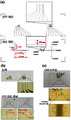
1 is a schematic view showing a microchip fabrication process using UV epoxy bonding. The upper plate was fabricated by patterning the microchannels on the lower plate and the electrodes on the lower plate, and the lower plate and the upper plate coated with UV epoxy were arranged in a desired position, and then bonded by UV exposure and washed electrochemically using sulfuric acid solution.
2 is a view showing the design of the electrode and the micro-channel according to an embodiment of the present invention. (a) shows a photo-mask design for an electrode and a microchannel pattern, the scale of which is as follows: from a sample (and sample-waste) reservoir to an injection channel, 6 mm to channel, 2 mm from buffer reservoir to double-T channel; Separation channel length. 16 mm; Effective length, 12 mm; PGSB channel, 350 μm. (b) shows an image of an electrode and a microchip channel. The channel width is 80 μm and the depth is 15 μm. The size of the double-T channels is 80 μm wide and 15 μm deep and includes an injection intersection of 100 μm. PGSB channels are 120 μm wide and 15 μm deep. The Au electrode has a width of 10 or 20 mu m. (c) is a microchip photograph for channel-electrochemical detection.
3 is a view comparing the area of the electrode calculated by the experiment after the electrochemical cleaning and the electrode area obtained through the imaging.
4 is a diagram showing the effect of electrochemical cleaning with 0.5 MH 2 SO 4 . (a) and (b) are cyclic voltammetry diagrams of Au disk electrodes before and after electrochemical cleaning with H 2 SO 4 , respectively. Au working electrode width is 10 μm and circulates potential between 0 and +0.5 V for Ag / AgCl at a scanning rate of 50 mV / s in a 5 mM K 3 Fe (CN) 6 solution containing 100 mM KNO 3 Cyclic voltammetry was performed.
Hereinafter, the present invention will be described in more detail with reference to Examples. These examples are for further illustrating the present invention, and the scope of the present invention is not limited to these examples.
Example
1: Fabrication of Microchips
A method of manufacturing a microchip using UV epoxy adhesion by traditional photolithography and photopolymerization is shown in FIG. 1. In the present invention, an electrophoretic microchip was manufactured as an example of the microchip. Patterning of channel and gold electrodes was made by the inventors similar to previous studies (Chun, H. G et al., Anal. Chem., 2005, 77: 2490-2495; Joo, S. et al. , Anal. Sci., 2007, 23: 277-281). Briefly, to form a microchannel pattern, a glass cover slide (Cat. No. 1000412, Paul Marienfeld, Germany) was first prepared using piranha solution (H 2 SO 4 : H 2 O 2 = 3: GmbH & Co. KG, Germany). (Note: Piranha solution should be handled with special care because it is a strong oxidant that reacts violently with organic compounds). Photoresist (AZ4620, Clariant, Switzerland) was spin coated on glass slides for 30 seconds at 7000 rpm. Subsequently, a photolithographic process including soft baking, UV exposure, development, hard baking, and wet etching was sequentially performed.
The design of the microchannels and the electrode images were made using AutoCAD (Fig. 2 (a)). Chung, TD, Biosens, J., Kim, KH, Kim, KH, et al. Bioelectron., 2010, 25: 1509-1515). Figures 2 (b) and 2 (c) are photographs of the fabricated microchip structure. The microchip consists of a channel-patterned glass substrate and an Au-deposited glass substrate. Microchip designs and fabrication results are shown in Fig. The Au electrode can be fabricated in various sizes for electrochemical studies under various electroplating conditions with the electrode scale shown in FIG.
Bottom glass slides were also fabricated using a similar photolithography protocol. The glass slides were washed with piranha solution and coated with hexamethyldisilazane (HMDS, Clariant, Switzerland) and then spin-coated with AZ5214 (Clariant, Switzerland) at 4000 rpm for 30 seconds. After prebaking at 100 ° C for 1 minute, exposure was performed at 17 mJ / cm 2 for 5 seconds, reversal baking at 100 ° C for 5 minutes, and then flood exposure at 17 mJ / cm 2 for 5 seconds to obtain AZ300MIF (Clariant, Switzerland). A metal film was sputtered on the patterned glass using a DC / RF electron tube sputter (Atron, Korea). A titanium (Ti) adhesive layer was sputtered to a thickness of about 350 Å, and a 5000 Å thick and 10-20 μm thick gold (Au) thin film was deposited thereon at 5 Å / s. The gold-patterned glass was immersed in acetone (JT Baker, USA) to remove the residue of the patterned Au / Ti layer. UV exposure was then used for the adhesion process. After washing with piranha solution and air blowing, the gold electrode pattern was spin coated with a UV curing resin (LOT No. A10K01, ThreeBond Co., Ltd., Japan) at 1500 rpm for 30 seconds. The substrate was exposed to ultraviolet light of 365 nm wavelength at 17 mJ / cm 2 for 12 seconds. The channel was then rinsed with acetone for 30 seconds. The bottom glass slides were electrochemically cleaned using Ag / AgCl and platinum wires as reference and counter electrodes, respectively, in a 0.5 M sulfuric acid solution at a circulating potential between +1.0 and +0.2 V. The pattern design of the microchip and the optical image of the fabricated chip are shown in Fig.
The final chip was made by bonding cover and bottom glass slide. After washing with sulfuric acid, the surface area of the gold electrode exposed to the microchannel was experimentally confirmed to be stable by acting as an electrode of the gold thin film. Gold surface area was measured by cyclic voltammetry in a 5 mM K 3 Fe (CN) 6 solution and was consistent with the area measured using a video microscope system (ICS-305B, Sometech, Korea) (FIG. 3).
Example
2:
UV
Gold electrode after epoxy bonding
Surface area
decision
The surface area of the gold electrode exposed on the inner wall of the channel was calculated using the limit current i lim by cyclic voltammetry. According to the microband electrode model, the limiting current is given by the following formula:

Where n is the number of electrons moved, F is the Faraday constant, D is the diffusion coefficient, l is the fine band length, w is the fine band width, t is the flow time and C is the bulk concentration of the electroactive species. 3 is a diagram illustrating a cyclic voltammetry measurement result obtained in a 5 mM K 3 Fe (CN) 6 solution containing 100 mM KNO 3 as an auxiliary electrolyte. It was confirmed that the area of the gold electrode calculated from the i lim value by the cyclic voltammetry was consistent with the value measured by the video image.
Example
3: additional on microchip
UV
Hardening
Effect of Sulfuric Acid Cleaning on Contaminated Gold Electrode Surfaces by Structure Introduction
The structure may be additionally introduced using UV resin as necessary on the microchip including the prepared electrode. The process of introducing the structure is generally filled with a raw material that can be cured by UV irradiation inside the microchannel to form the structure, and then irradiated with light to a desired position using a photomask to form the structure and the uncured excess After removing the material of the organic solvent and the like proceeds by washing the channel. In this case, when contaminants remain on the exposed electrode in the channel, or when the organic solvent for cleaning may cause self-contamination or incomplete cleaning, this may reduce the stability and / or sensitivity of the electrode have.
Therefore, in order to confirm the cleaning effect of sulfuric acid on the surface of the contaminated gold electrode after the introduction of additional materials on the microchip including the prepared electrode, a polymer electrolyte formed by curing by exposing to UV on a disk electrode (disk) The same procedure as for forming a gel polyelectrolyte was performed, followed by electrochemical washing using a 0.5 M sulfuric acid solution. Surface treatment methods are as follows:
A gold disc electrode with a radius of 3 mm was washed with a piranha solution and immersed in 0.1 M TMSMA (3- (trimethoxysilyl) propylmethacrylate) solution for 20 minutes. The TMSMA-coated electrode was immersed in 2.5M AMPSA (2-acrylamido-2-methyl-1-propanesulfonic acid) monomer solution for 10 minutes.
Figure 4 shows a cyclic voltammetry measured after the electrochemical cleaning method with an electrode before treatment with the chemical and sulfuric acid solution after the chemical treatment. It was confirmed that the cyclic voltammetry of the gold disc electrode washed with sulfuric acid solution was consistent with that of pure gold disc electrode without chemical treatment. Thus, as shown in Figure 4 it was confirmed that the chemically contaminated gold electrode can be effectively washed by the electrochemical method using sulfuric acid solution.
Claims (14)
A second step of washing the interior by flowing an organic solvent through a microchannel; And
And a third step of electrochemically cleaning the electrode surface exposed to the inside of the microchannel with an acid solution.
The organic solvent of the second step is selected from the group consisting of acetone, methanol, ethanol, n-propanol, isopropanol and mixed solvents thereof.
The third step is a method for manufacturing a chip that electrochemically cleans the surface of the electrode exposed inside the microchannel by a cyclic voltammetry that fills the acidic solution in the microchannel and applies a voltage to the electrode.
The chip is a method of manufacturing a chip in which the first substrate substrate patterned electrode and the second substrate patterned microchannel.
Bonding of the first substrate and the second substrate is a chip manufacturing method of the photocurable resin.
The washing step is to remove the reactants used for the adhesion and by-products therefrom.
The electrode is a method of manufacturing a chip formed by depositing an electrode material through photolithography.
Wherein the electrode material is selected from the group consisting of gold, platinum, palladium, silver, copper, metal oxides, carbon, indium tin oxide (ITO), and semiconducting materials.
The microchannel is formed by a wet or dry etching method after performing the photolithography.
The washing step is to remove the unreacted residues and reaction by-products from the photolithography reactants and by-products derived therefrom or the structure introduced into the microchannel after the chip is used in the manufacture of the chip is produced Way.
PH of the acid solution is 1 to 5 method for producing a chip.
The electrochemical cleaning step is a chip manufacturing method that is performed by cyclic voltammetry (CV).
The chip is a method of manufacturing a chip that is a microchip or a nanochip.
Priority Applications (1)
| Application Number | Priority Date | Filing Date | Title |
|---|---|---|---|
| KR1020120064103A KR20130141032A (en) | 2012-06-15 | 2012-06-15 | A method for cleaning a microchip with electrodes and microchannels |
Applications Claiming Priority (1)
| Application Number | Priority Date | Filing Date | Title |
|---|---|---|---|
| KR1020120064103A KR20130141032A (en) | 2012-06-15 | 2012-06-15 | A method for cleaning a microchip with electrodes and microchannels |
Publications (1)
| Publication Number | Publication Date |
|---|---|
| KR20130141032A true KR20130141032A (en) | 2013-12-26 |
Family
ID=49985245
Family Applications (1)
| Application Number | Title | Priority Date | Filing Date |
|---|---|---|---|
| KR1020120064103A KR20130141032A (en) | 2012-06-15 | 2012-06-15 | A method for cleaning a microchip with electrodes and microchannels |
Country Status (1)
| Country | Link |
|---|---|
| KR (1) | KR20130141032A (en) |
Cited By (1)
| Publication number | Priority date | Publication date | Assignee | Title |
|---|---|---|---|---|
| WO2020065042A1 (en) * | 2018-09-28 | 2020-04-02 | Klearia | Method for cleaning and/or regenerating a glass microfluidic sensor for the analysis of metals |
-
2012
- 2012-06-15 KR KR1020120064103A patent/KR20130141032A/en not_active Application Discontinuation
Cited By (2)
| Publication number | Priority date | Publication date | Assignee | Title |
|---|---|---|---|---|
| WO2020065042A1 (en) * | 2018-09-28 | 2020-04-02 | Klearia | Method for cleaning and/or regenerating a glass microfluidic sensor for the analysis of metals |
| FR3086554A1 (en) * | 2018-09-28 | 2020-04-03 | Klearia | METHOD FOR CLEANING AND / OR REGENERATION OF A GLASS MICROFLUIDIC SENSOR FOR METAL ANALYSIS |
Similar Documents
| Publication | Publication Date | Title |
|---|---|---|
| Schneider et al. | Wettability patterning by UV-initiated graft polymerization of poly (acrylic acid) in closed microfluidic systems of complex geometry | |
| Bhagat et al. | Photodefinable polydimethylsiloxane (PDMS) for rapid lab-on-a-chip prototyping | |
| KR101402402B1 (en) | Method for manufacturing substrate for making microarray | |
| Sudarsan et al. | Printed circuit technology for fabrication of plastic-based microfluidic devices | |
| JP2004284225A (en) | Manufacturing method of resin molded article, manufacturing method of metal structure, and chip | |
| US11878299B2 (en) | Imprinted substrates | |
| Yu et al. | Oxygen reduction reaction induced pH-responsive chemo-mechanical hydrogel actuators | |
| EP1431018A1 (en) | Method of producing resin molded product | |
| KR20130125686A (en) | An electrophoresis chip for electrochemical detection | |
| Hemanth et al. | Pyrolytic 3D carbon microelectrodes for electrochemistry | |
| KR20130141032A (en) | A method for cleaning a microchip with electrodes and microchannels | |
| US8420181B2 (en) | Method of producing microfluidic devices based on a polymer | |
| Cheng et al. | Design and fabrication of a hybrid nanofluidic channel | |
| Middya et al. | Lithography and electrodes | |
| Mamun et al. | Patterning of platinum microelectrodes in polymeric microfluidic chips | |
| JP4966694B2 (en) | Manufacturing method of microstructured mold | |
| JP4944640B2 (en) | Manufacturing method of microstructured mold | |
| JP4769544B2 (en) | Manufacturing method of secondary mold | |
| Kole et al. | Rapid prototyping of nanofluidic slits in a silicone bilayer | |
| Alvankarian et al. | Low cost prototyping of microfluidic structure | |
| KR101402584B1 (en) | Method for manufacturing substrate for making microarray | |
| KR100901195B1 (en) | Method for fabricating micro pattern on a plastic substrate | |
| Sayah et al. | LF55GN photosensitive flexopolymer: a new material for ultrathick and high-aspect-ratio MEMS fabrication | |
| García et al. | Micro-molding for poly (dimethylsiloxane) microchips | |
| Zhang | Fabrication of very high aspect micromold by SU-8 photolithography and electroforming |
Legal Events
| Date | Code | Title | Description |
|---|---|---|---|
| A201 | Request for examination | ||
| E902 | Notification of reason for refusal | ||
| E601 | Decision to refuse application |