KR20130052555A - Method of manufacturing a panel with occluded microholes and products made thereby - Google Patents
Method of manufacturing a panel with occluded microholes and products made thereby Download PDFInfo
- Publication number
- KR20130052555A KR20130052555A KR1020127026686A KR20127026686A KR20130052555A KR 20130052555 A KR20130052555 A KR 20130052555A KR 1020127026686 A KR1020127026686 A KR 1020127026686A KR 20127026686 A KR20127026686 A KR 20127026686A KR 20130052555 A KR20130052555 A KR 20130052555A
- Authority
- KR
- South Korea
- Prior art keywords
- light transmissive
- polymer material
- exposure
- panel
- micro holes
- Prior art date
Links
Images


Classifications
-
- F—MECHANICAL ENGINEERING; LIGHTING; HEATING; WEAPONS; BLASTING
- F21—LIGHTING
- F21V—FUNCTIONAL FEATURES OR DETAILS OF LIGHTING DEVICES OR SYSTEMS THEREOF; STRUCTURAL COMBINATIONS OF LIGHTING DEVICES WITH OTHER ARTICLES, NOT OTHERWISE PROVIDED FOR
- F21V11/00—Screens not covered by groups F21V1/00, F21V3/00, F21V7/00 or F21V9/00
-
- G—PHYSICS
- G02—OPTICS
- G02B—OPTICAL ELEMENTS, SYSTEMS OR APPARATUS
- G02B6/00—Light guides; Structural details of arrangements comprising light guides and other optical elements, e.g. couplings
-
- F—MECHANICAL ENGINEERING; LIGHTING; HEATING; WEAPONS; BLASTING
- F21—LIGHTING
- F21S—NON-PORTABLE LIGHTING DEVICES; SYSTEMS THEREOF; VEHICLE LIGHTING DEVICES SPECIALLY ADAPTED FOR VEHICLE EXTERIORS
- F21S2/00—Systems of lighting devices, not provided for in main groups F21S4/00 - F21S10/00 or F21S19/00, e.g. of modular construction
-
- G—PHYSICS
- G02—OPTICS
- G02B—OPTICAL ELEMENTS, SYSTEMS OR APPARATUS
- G02B6/00—Light guides; Structural details of arrangements comprising light guides and other optical elements, e.g. couplings
- G02B6/0001—Light guides; Structural details of arrangements comprising light guides and other optical elements, e.g. couplings specially adapted for lighting devices or systems
-
- H—ELECTRICITY
- H05—ELECTRIC TECHNIQUES NOT OTHERWISE PROVIDED FOR
- H05K—PRINTED CIRCUITS; CASINGS OR CONSTRUCTIONAL DETAILS OF ELECTRIC APPARATUS; MANUFACTURE OF ASSEMBLAGES OF ELECTRICAL COMPONENTS
- H05K5/00—Casings, cabinets or drawers for electric apparatus
- H05K5/02—Details
-
- Y—GENERAL TAGGING OF NEW TECHNOLOGICAL DEVELOPMENTS; GENERAL TAGGING OF CROSS-SECTIONAL TECHNOLOGIES SPANNING OVER SEVERAL SECTIONS OF THE IPC; TECHNICAL SUBJECTS COVERED BY FORMER USPC CROSS-REFERENCE ART COLLECTIONS [XRACs] AND DIGESTS
- Y10—TECHNICAL SUBJECTS COVERED BY FORMER USPC
- Y10T—TECHNICAL SUBJECTS COVERED BY FORMER US CLASSIFICATION
- Y10T428/00—Stock material or miscellaneous articles
- Y10T428/24—Structurally defined web or sheet [e.g., overall dimension, etc.]
- Y10T428/24273—Structurally defined web or sheet [e.g., overall dimension, etc.] including aperture
-
- Y—GENERAL TAGGING OF NEW TECHNOLOGICAL DEVELOPMENTS; GENERAL TAGGING OF CROSS-SECTIONAL TECHNOLOGIES SPANNING OVER SEVERAL SECTIONS OF THE IPC; TECHNICAL SUBJECTS COVERED BY FORMER USPC CROSS-REFERENCE ART COLLECTIONS [XRACs] AND DIGESTS
- Y10—TECHNICAL SUBJECTS COVERED BY FORMER USPC
- Y10T—TECHNICAL SUBJECTS COVERED BY FORMER US CLASSIFICATION
- Y10T428/00—Stock material or miscellaneous articles
- Y10T428/24—Structurally defined web or sheet [e.g., overall dimension, etc.]
- Y10T428/24802—Discontinuous or differential coating, impregnation or bond [e.g., artwork, printing, retouched photograph, etc.]
Abstract
본 발명은 패널 제조 방법 및 이에 따라 제조되는 패널에 관한 것이다. 패널은 일 패턴으로 배열되며 광 투과성 폴리머 재료로 충전되는 복수 개의 마이크로 홀을 포함한다. 광 투과성 폴리머 재료가 마이크로 홀을 막도록 사용되며, 휴지기를 사이에 두고 서로 별개로 분리 수행되는 적어도 두 번의 노광 주기를 사용하여 에너지 공급원에 노출되는 방식으로 경화된다.The present invention relates to a method for producing a panel and a panel produced accordingly. The panel includes a plurality of micro holes arranged in one pattern and filled with a light transmissive polymer material. The light transmissive polymer material is used to block the micro holes and is cured in such a way that it is exposed to an energy source using at least two exposure cycles which are performed separately from each other with a resting period in between.
Description
본 발명은, 개괄적으로 설명하자면, 막힌 상태의 마이크로 홀을 구비한 패널을 제조하기 위한 방법 및 이에 따라 제조되는 제품에 관한 것이다.The present invention relates, in general, to a method for producing a panel with a microhole in a blocked state and to a product produced accordingly.
정보 제공을 목적으로 하우징을 관통하여 등(light)을 돌출 설치하는 방법이 흔히 사용되고 있다. 이러한 예에는, 이로만 제한되는 것은 아니지만, "캡스락(Caps Lock)" 또는 "넘락(Num Lock)"과 같은 소정 기능을 나타내는 지시등을 포함하는 컴퓨터 키보드와, "온/오프(on/off)" 등을 포함하는 컴퓨터 모니터와, 가열 시트가 작동 상태인지 비작동 상태인지 또는 에어 백이 작동 상태인지 비작동 상태인지를 지시해 주는 등을 포함하는 자동차, 지시등을 구비한 텔레비젼, 그리고 그외 다른 수많은 전자 기기가 포함된다.For the purpose of providing information, a method of projecting a light through a housing is commonly used. Examples include, but are not limited to, a computer keyboard including indicator lights that indicate certain functions, such as "Caps Lock" or "Num Lock," and "on / off." Cars, televisions with indicator lights, and many other electronics, including computer monitors including lights, and indicating whether the heating sheet is in operation or inactive, or whether the airbag is in operation or inactive. The device is included.
전술한 바와 같은 지시등을 제공하기 위하여, 일반적으로, 돌출 등을 제공하는 방법이 사용되고 있으며, 이러한 돌출 등은 등이 꺼져 있는 상태에서도 볼 수 있으면서 등이 켜져 있는 상태에서는 이를 나타내기 위해 밝게 빛나게 된다. 등 집합체나 등의 설치 홀은 산업 디자이너가 원하는 목적을 달성하는데 방해가 될 수도 있다. In order to provide the indicator light as described above, a method of providing a projection lamp is generally used, and the projection lamp is brightly displayed to indicate this when the lamp is turned on while being visible even when the lamp is turned off. The back assembly or the back mounting hall may interfere with the industrial designer's purpose.
가시성이 더 약한 등의 설치를 위한 홀을 형성하기 위한 일 방법은 매우 작은 테이퍼형 홀을 천공한 다음 이 홀을 투명한 재료로 충전하는 것이다. 이러한 홀은 기계적 천공, 레이저, 방전 기계 가공 또는 화학적 에칭 방법을 사용하여 형성될 수 있다. 이러한 홀을 형성하기 위한 일 방법이 본 발명의 양수인에게 양도된 동시 계류 중인 미국 특허 출원 제 11/742,862 호에 개시되어 있다. 개괄적으로 말하여, 상기 출원에 개시된 방법은 실질적으로 불투명한 패널 또는 유사한 물품을 관통하여 해당 명세서에서 비아(via)라고도 불리우는 홀을 천공하는 단계와, 상기 홀을 투명한 재료로 충전하는 단계와, 상기 충전 재료를 경화시키는 단계, 그리고 물품의 관찰 표면(viewing surface)으로부터 과잉 재료를 제거하여 표면을 세정하는 단계를 포함한다. One way to form a hole for installation, such as having less visibility, is to drill a very small tapered hole and then fill the hole with a transparent material. Such holes may be formed using mechanical drilling, laser, discharge machining or chemical etching methods. One method for forming such a hole is disclosed in co-pending US patent application Ser. No. 11 / 742,862, assigned to the assignee of the present invention. In general terms, the method disclosed in this application comprises the steps of perforating a hole, also referred to herein as a via, through a substantially opaque panel or similar article, filling the hole with a transparent material, Curing the fill material and removing the excess material from the viewing surface of the article to clean the surface.
본 발명의 실시예는 광의 조사 시에 패널의 막힌 상태의 마이크로 홀의 외관 개선을 다루고 있다. 보다 구체적으로, 본 명세서에서 설명되고 있는 방법에 따르면, 막힌 상태의 마이크로 홀이 광도 및/또는 광학 직경에 대하여 개선된 균일도를 갖추도록 할 수 있다. 이러한 방법에 의해 제조되는 제품이 또한 설명되어 있다. 본 명세서에서, 마이크로 홀은 패널 또는 일 표면으로부터 다른 표면으로 연장되는 그외 다른 하우징 부분에 형성되는 홀을 일컫는 것으로, 이러한 홀은 내벽(들)과, 홀이 관통되는 표면과 동일 평면에 의해 경계가 획정되는 내부 체적을 갖는다. 마이크로 홀은 후술하는 바와 같이 치수가 작으며, 가시광 투과 재료, 바람직하게는 투명 재료로 충전된다.Embodiments of the present invention deal with improving the appearance of the microholes in the blocked state of the panel when irradiated with light. More specifically, according to the methods described herein, it is possible to ensure that the blocked micro holes have improved uniformity with respect to light intensity and / or optical diameter. Also described are products produced by this method. As used herein, micro holes refer to holes formed in a panel or other housing portion extending from one surface to another surface, which holes are bounded by the inner wall (s) and the same plane as the surface through which the holes pass. Has a defined internal volume. The microholes are small in dimensions as described below and are filled with a visible light transmitting material, preferably a transparent material.
본 발명의 일 실시예에 따른 패널 제조 방법이 설명되어 있다. 이러한 방법은, 예를 들어, 일 패턴으로 배열되는 복수 개의 마이크로 홀을 광 투과성 폴리머 재료(polymeric material)를 이용하여 막는 단계로서, 상기 광 투과성 폴리머 재료는 유동 가능한 상태에 있으며, 상기 복수 개의 마이크로 홀은 상기 패널의 실질적으로 평면형 영역의 제 1 표면의 제 1 개구로부터 상기 제 1 표면의 반대쪽의 상기 실질적으로 평면형 영역의 제 2 표면의 제 2 개구까지 연장되고, 상기 제 1 개구 및 제 2 개구 각각의 직경은 상기 실질적으로 평면형 영역의 두께보다 작은, 상기 복수 개의 마이크로 홀을 막는 단계, 그리고 상기 가시광 투과성 폴리머 재료를 제 1 노광 주기 동안 공급원에 노출시키고, 상기 제 1 노광 주기 이후 상기 광 투과성 폴리머 재료가 상기 공급원에 노출되지 않는 제 1 휴지기를 제공하며, 상기 제 1 휴지기 이후 제 2 노광 주기 동안 상기 광 투과성 폴리머 재료를 상기 공급원에 노출시킴으로써, 상기 복수 개의 마이크로 홀을 막고 있는 상기 광 투과성 폴리머 재료를 유동 가능한 상태로부터 상기 광 투과성 폴리머 재료가 상기 복수 개의 마이크로 홀의 내면에 고정되는 경화 상태로 경화 처리하는 단계를 포함한다. A panel manufacturing method according to an embodiment of the present invention is described. Such a method is, for example, blocking a plurality of micro holes arranged in a pattern using a light transmissive polymer material, wherein the light transmissive polymer material is in a flowable state and the plurality of micro holes Extends from the first opening of the first surface of the substantially planar region of the panel to the second opening of the second surface of the substantially planar region opposite the first surface, each of the first opening and the second opening; Blocking the plurality of micro holes, wherein the diameter of the substantially planar region is less than the thickness, and exposing the visible light transmissive polymer material to a source during a first exposure period, the light transmissive polymer material after the first exposure period. Provides a first resting period that is not exposed to the source, wherein Curing the light transmissive polymer material to be fixed to an inner surface of the plurality of micro holes from a state in which the light transmissive polymer material blocking the plurality of micro holes is flowable by exposing the light transmissive polymer material to the source for two exposure cycles. Curing treatment in a state.
본 발명의 다른 실시예에 따른, 전술한 방법에 의해 형성되는 패널이 설명된다. 이러한 일 패널은 제 1 평면형 표면과 이 제 1 평면형 표면의 반대쪽 제 2 평면형 표면을 포함하는 실질적으로 평면형 부분과, 상기 제 1 평면형 표면으로부터 상기 제 2 평면형 표면으로 관통하여 형성되며, 각각 개개의 평면형 표면에 형성되는 제 1 및 제 2 개구와 연통하고, 상기 평면형 표면 사이에 내면을 구비하는 복수 개의 마이크로 홀, 그리고 각각의 마이크로 홀의 내부에 배치되며, 몸체의 제 1 평면형 표면과 실질적으로 동일 평면의 제 1 외면과, 상기 제 1 외면 반대쪽의 제 2 외면, 그리고 이들 외면 사이에 배치되는 중앙 몸체를 포함하는 광 투과성 폴리머 재료를 포함한다. 이러한 실시예에 있어서, 상기 광 투과성 폴리머 재료의 중앙 몸체는 상기 내면과 접촉 결합하는 중앙 외면을 구비하며, 상기 광 투과성 폴리머 재료는, 성분 중 적어도 5%가 휴지기를 사이에 두고 분리 수행되는 적어도 두 번의 UV 노광 주기에 노출된 UV 경화 가능한 에폭시 아크릴레이트 올리고머로부터 유도되는, 폴리머 체인을 포함한다.According to another embodiment of the present invention, a panel formed by the above-described method is described. One such panel is formed through a substantially planar portion comprising a first planar surface and a second planar surface opposite the first planar surface, and penetrating from the first planar surface to the second planar surface, each planar A plurality of micro holes in communication with the first and second openings formed in the surface and having an inner surface between the planar surfaces, and disposed inside each micro hole and substantially coplanar with the first planar surface of the body. And a light transmitting polymer material comprising a first outer surface, a second outer surface opposite the first outer surface, and a central body disposed between these outer surfaces. In this embodiment, the central body of the light transmissive polymer material has a central outer surface in contact with the inner surface, the light transmissive polymer material having at least two separations performed at least 5% of the components with a resting period between them. Polymer chains derived from UV curable epoxy acrylate oligomers exposed to one UV exposure cycle.
본 명세서에는 또한, 이러한 실시예의 변형예 및 세부 사항 그리고 그외 다른 실시예가 설명되어 있다. Also described herein are variations and details of these embodiments and other embodiments.
이하, 여러 개의 도면에 걸쳐 동일한 부품이 동일한 도면 부호로 지시되어 있는 첨부 도면을 참조하여 본 발명이 설명된다:
도 1은 패널에 마이크로 홀을 레이저 천공하는 과정을 개략적으로 나타낸 도면;
도 2는 패널에 천공된 마이크로 홀을 충전하는 과정을 개략적으로 나타낸 도면;
도 3은 본 발명의 일 실시예에 따른, 패널에 천공된 마이크로 홀을 충전하도록 사용되는 재료의 경화 과정을 개략적으로 나타낸 도면;
도 4는 코스메틱측으로부터 재료를 세정한 후의 도 3의 패널을 개략적으로 나타낸 도면;
도 5는 패널을 레이저 천공한 이후 마이크로 홀을 충전하기 이전의 원추형 마이크로 홀의 기하학적 형태를 개략적으로 나타낸 도면;
도 6은 충전 재료의 노광 처리 횟수 대비 충전 상태의 마이크로 홀로부터 방출되는 광의 정규 균일도를 나타낸 비교 그래프;
도 7은 충전 재료의 노광 처리 횟수 대비 충전 상태의 마이크로 홀의 정규 직경을 나타낸 비교 그래프;
도 8은 동일 노광량을 기준으로 휴지기가 있는 경우 및 없는 경우의 충전 상태의 마이크로 홀로부터 방출되는 광의 정규 균일도를 나타낸 비교 그래프;
도 9는 동일 노광량을 기준으로 휴지기가 있는 경우 및 없는 경우의 충전 상태의 마이크로 홀의 광학 직경을 나타낸 비교 그래프;
도 10은 동일 노광량을 기준으로 휴지기가 상이한 경우의 충전 상태의 마이크로 홀로부터 방출되는 광의 정규 균일도를 나타낸 비교 그래프; 그리고
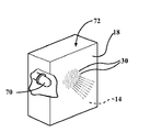
도 11은 충전 상태의 마이크로 홀을 포함하는 광 투과성 패널을 사용하는 하우징을 개략적으로 나타낸 도면.The invention is now described with reference to the accompanying drawings, wherein like parts are designated by like reference numerals throughout the several views of the drawings:
1 is a view schematically illustrating a process of laser drilling micro holes in a panel;
2 is a view schematically illustrating a process of filling a perforated micro hole in a panel;
3 schematically illustrates the curing process of a material used to fill a perforated micro hole in a panel, in accordance with an embodiment of the present invention;
4 schematically shows the panel of FIG. 3 after cleaning the material from the cosmetic side;
5 is a schematic representation of the geometry of the conical micro holes after laser drilling of the panel and before filling the micro holes;
6 is a comparison graph showing the normal uniformity of light emitted from the microholes in the charged state compared to the number of exposure treatments of the filling material;
7 is a comparison graph showing normal diameters of micro holes in a filled state compared to the number of exposure treatments of a filling material;
8 is a comparison graph showing the normal uniformity of light emitted from the microholes in the charged state with and without the resting period on the basis of the same exposure amount;
9 is a comparison graph showing the optical diameter of the micro holes in the charged state with and without the resting period based on the same exposure amount;
10 is a comparison graph showing the normal uniformity of light emitted from the microholes in the charged state when the resting period is different based on the same exposure amount; And
FIG. 11 is a schematic representation of a housing using a light transmissive panel including micro holes in a charged state. FIG.
미국 특허 출원 제 11/742,862 호에는, 후방으로부터의 광 조사 시에 광을 통과시킬 수 있는 천공부를 포함하지만, 광원의 부재 시에 외관상 주변 재료와 비교적 구별되지 않을 정도로 크기가 작은 홀을 또한 포함하는 하우징 또는 패널을 제조하기 위한 방법이 개시되어 있다. 다시 말해, 전술한 바와 같은 홀은 후방으로부터 광이 조사되지 않는 경우 실질적으로 육안으로는 확인할 수 없다.US patent application Ser. No. 11 / 742,862 also includes perforations capable of passing light upon irradiation of light from the rear, but also includes holes that are small in appearance in the absence of the light source so as to be relatively indistinguishable from the surrounding materials. A method for manufacturing a housing or panel is disclosed. In other words, the hole as described above can not be visually confirmed when the light is not irradiated from the rear.
그러나, 전술한 홀은 후방으로부터의 광 조사 시에 불균일한 광도 및/또는 광학 직경을 나타낼 수 있다. 본 발명의 발명자가 제시한 이론에 따르면, 경화 처리 과정에서 UV 경화 가능한 충전 재료 내부에서 발생되는 열이 전술한 바와 같은 특성의 균일도에 악영향을 미치게 된다. 이러한 문제를 해결하기 위하여, 본 발명에 따른 방법이 개발되었다. However, the holes described above may exhibit non-uniform luminous intensity and / or optical diameter upon light irradiation from the rear. According to the theory presented by the inventor of the present invention, the heat generated inside the UV curable filling material during the curing treatment adversely affects the uniformity of the characteristics as described above. In order to solve this problem, a method according to the present invention has been developed.
이하, 본 발명의 실시예가 도 1 내지 도 11을 참조하여 가장 용이한 방식으로 설명된다. 도 1 내지 도 5에 도시된 바와 같은 패널(12)은 소정 재료로 형성되는 비교적 얇은 연속적인 시트로서, 필수 요건은 아니지만, 금속 시트로 형성되는 것이 바람직하다. 이러한 패널(12)은 패널의 두께(20)를 획정하는 제 1 표면 또는 후면(14)과, 반대쪽의 제 2 표면 또는 전면(18)을 포함한다. 전면(18)은 비교적 평활하며, 광원으로부터 전면에 천공되어 있는 마이크로 홀(30)로 광이 조사되지 않는 경우 육안으로 보기에 실질적으로 연속적인 형태이다. 이러한 전면(18)은 또한, 본 명세서에서 코스메틱 표면(18)이라고도 칭한다. 패널(12)은 통상, 양극 산화 알루미늄과 같은 금속으로 형성되지만, 플라스틱이나 합성 재료와 같은 그외 다른 재료가 사용될 수도 있다. 패널(12)이 시트 재료로 형성되는 것으로 설명되어 있긴 하지만, 본 발명이 반드시 이러한 예로만 제한되는 것은 아님에 주목하여야 한다. 예를 들어, 패널(12)이 모서리, 곡선형 외면 등을 구비한 하우징 부분이나 리드(lid) 등일 수도 있다. 그러나, 패널(12)의 각각의 천공부는 비교적 균일한 두께를 갖는 것이 바람직하다.Embodiments of the present invention will now be described in the easiest manner with reference to FIGS. The
마이크로 홀(30)은, 도 1에 도시된 바와 같이, 후면(14)으로부터 코스메틱 표면(18)으로 연장된다. 마이크로 홀(30)의 개수는 특히 제한되어 있는 것은 아니며, 후면(14)으로부터 마이크로 홀(30)로 광이 투사되는 경우 코스메틱 표면(18)의 방향에서 육안으로 볼 수 있는 소정의 메시지, 패턴 등을 형성하도록 하기에 충분한 개수로만 형성되면 된다. 패널에 마이크로 홀(30)을 천공 또는 기계 가공하기 위한 일 방법에 따르면, 다이오드 펌핑 고체 상태 펄스형 레이저(diode-pumped solid-state pulsed laser)와 같은 레이저(24)가 원형 또는 나선형(트리패닝(trepanning)) 패턴으로 인가된다. 밝혀진 바에 따르면, 30kHz의 펄스 반복률 및 60 나노초 펄스폭을 갖는 Nd;YAG 355nm 스폿(22)이 마이크로 홀(30)의 기계 가공에 유용하다. 도시된 바와 같이, 패널(12)을 관통하여 후면(14)으로부터 코스메틱 표면(18)으로 천공이 이루어진다. 그외에도, 당 업계의 숙련자에게는 공지되어 있는 상이한 특성을 갖는 다른 유형의 레이저 및 다른 기계 가공 공정이 패널(12)의 두께 및 특정 용례에 맞추어 사용될 수도 있다. The
도 5에는 전술한 바와 같이 천공된 하나의 마이크로 홀(30)이 도시되어 있다. 마이크로 홀(30)은 전면(14)의 제 1 개구(40)와 반대쪽 코스메틱 표면(18)의 제 2 개구(44) 사이의 원추형 측벽(34)에 의해 형성된다. 제 1 개구(40)의 직경이 제 2 개구(44)의 직경보다 크다. 마이크로 홀(30)이란 명칭은 각각의 개구(40, 44)의 직경이 대략 100㎛를 초과하지 않는 것이 바람직함에 따라 붙여진 것이다. 예를 들어, 도 5에 도시된 바와 같이, 제 1 개구(40)의 직경은 대략 90~100㎛이며, 제 2 개구(44)의 직경은 대략 30~40㎛이다.5 shows one
기계 가공 공정을 통해 그외 다른 형상 및 구성이 초래할 수도 있음을 이해하여야 한다. 예를 들어, 제 1 개구(40)와 제 2 개구(44)는 실질적으로 크기가 유사할 수 있다. 또한, 크기가 보다 크거나 작은 마이크로 홀(30)이 형성될 수도 있다. 그러나, 코스메틱 표면(18)의 제 2 개구(44)는 후방으로부터 광이 조사되지 않는 경우 실질적으로 육안으로는 마이크로 홀(30)을 볼 수 없도록 형성되어야 한다. 예를 들어, 관찰 표면으로부터 비교적 가까운 20~25cm의 거리에서는 확대경이나 현미경 없이 대략 0.05mm(50㎛)의 물체까지도 볼 수 있다. 좀 더 먼 보통의 시야 범위(대략 30cm 정도)에서 크기가 더 큰 홀(예를 들어, 1mm)이 보이지 않을 수도 있듯이 소형 물체의 가시성이 거리가 멀어질수록 감소하긴 하지만, 제 2 개구(44)의 직경은 대략 50㎛를 초과하지 않는 것이 바람직하다. It should be understood that other shapes and configurations may result from the machining process. For example,
제 2 개구(44)의 크기가 작은 것이 바람직하긴 하지만, 여러 가지 요인으로 인해 제 2 개구는 크기가 제한되어 있다. 예를 들어, 각각의 마이크로 홀(30)은 충전 재료에 의해 완전히 충전될 수 있으며 이러한 충전 상태에서도 제 1 개구(40)로부터 제 2 개구(44)를 통하여 광이 투사될 수 있을 정도의 종횡비를 갖추어야 한다. 따라서, 패널(12)의 두께와 충전 재료의 조성은 전술한 바와 같이 개구의 크기를 제한하는 일 요인이 될 수 있다. 또한, 마이크로 홀(30)의 크기는 마이크로 홀을 천공하도록 사용되는 기술에 의해 제한을 받는다. 제 1 개구(40)의 크기 또한, 유사한 요인으로 인해 제한을 받긴 하지만, 개구로 전달되는 광이 제 2 개구(44)에 도달할 수 있도록 하기에 충분할 정도로 크기가 더 커야 한다. 도시된 예에서, 패널(12)의 두께는 대략 400㎛이다. 패널(12)의 두께는 제 1 및 제 2 개구(40, 44)의 직경보다 커야 한다.Although it is desirable that the size of the
임의로, 마이크로 홀(30)은 기계 가공 공정 동안 형성되는 파편 또는 퇴적물을 제거하기 위하여 천공 후 세정될 수 있다. 이에 따라, 공지된 방법을 사용하여 세정 공정이 수행될 수 있다.Optionally, the
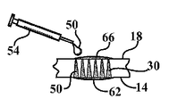
마이크로 홀(30)의 천공 및 임의의 세정 완료 후, 마이크로 홀(30)을 충전하거나 막기 위해 패널에 충전 재료(50)가 도포된다. 여기서, 홀을 막는 과정은 마이크로 홀(30)의 단면을 완전히 충전하는 방식으로 각각의 마이크로 홀(30)의 내부 체적부로 재료를 주입하는 것을 의미한다. 내부 체적부 전체를 완전히 충전할 수는 없음에 주목하여야 한다. 그러나, 일반적으로, 개구(40, 44) 중 적어도 하나를 초과하여 연장하는 과잉 재료가 존재하게 된다. 도 2에서, 예를 들어, 충전 재료(50)의 과잉 퇴적물(62)이 제 1 표면(14)을 따라 연장되며, 충전 재료(50)의 과잉 퇴적물(66)이 코스메틱 표면(18)을 따라 연장되고 있다.After completion of the puncture and any cleaning of the
도시된 바와 같이, 충전 재료(50)가 주사기 타입 장치(54)를 사용하여 마이크로 홀(30)의 임의의 크기가 더 작은 제 2 개구(44)의 위쪽으로 코스메틱 표면(18)에 도포된다. 예시되고 있는 액상 충전 재료(50)의 비교적 낮은 점성과, 원추형 마이크로 홀(30)의 기하학적 형상 그리고 중력으로 인해, 충전 재료(50)가 마이크로 홀(30)의 내부로 마이크로 홀을 관통하여 코스메틱 표면(18)으로부터 후면(14)으로 유동함으로써 마이크로 홀(30)이 막히게 된다. 유동 가능한 상태, 액체 상태, 또는 그외 다른 상태의 충전 재료(50)를 사용하여 마이크로 홀(30)을 막기 위해 그외 다른 기술이 사용될 수도 있다. 이러한 기술의 예에는, 잉크-젯(ink-jet) 기술 및 패드-프린팅(pad-printing) 기술이 포함된다. 또한, 충전 재료(50)가 코스메틱 표면(18)의 위에서 브러싱(brushing) 처리될 수 있다. 또한, 수동 주사기 장치(54)로서 도시되어 있긴 하지만, 패널(12)을 가로질러 주사기의 이동을 제어하며 각각의 액적의 분배량을 제어하는 컴퓨터 제어 분배 시스템이 장치(54)로서 사용될 수 있다.As shown, fill
여기서, 충전 재료(50)는 광학적으로 투명하며, 자외선(UV) 경화 가능한 아크릴레이트 폴리머로서, 패널(12)에 도포되는 시점에 액상을 유지한다. 바람직한 일 예의 가시광 투과 재료로서, 경화 시에 실질적으로 투명한, 미국 미네소타주 세인트 폴(St. Paul, Minnesota)에 소재하는 3M 컴퍼니에 의해 제조되는 AHS-1100을 상품명으로 하는 개발 재료가 있다. 경화란, 충전 재료(50)가 마이크로 홀(30)을 충전하도록 사용될 수 있는 유동 가능한 상태로부터, 통상 마이크로 홀(30) 내부에서 제자리에 유지되도록 측벽(34)에 부착되는 고체 상태 또는 비교적 단단한 상태로 변형되도록 하는 과정을 일컫는다. 충전 재료(50)가 유동 가능한 상태에 있다는 것은, 마이크로 홀의 내부 형상에 맞춰짐으로써 마이크로 홀(30)을 밀봉하도록 마이크로 홀(30)의 내부로 주입되거나 그외 다른 방식으로 삽입될 수 있도록 충전 재료가 가소성(예를 들어, 액체) 상태에 있다는 것을 의미한다. 충전 재료(50)가 패널(12)에 그리고 마이크로 홀(30)의 내부에 균일하면서도 평활하게 도포되도록 충전 재료(50)는 광 투과성의 주재료의 점성을 증가 또는 감소시키는 점성제를 혼합하여 형성될 수도 있다. 바람직한 일 예의 가시광 투과 재료에 추가하여, UV 방사선이 아닌 다른 수단에 의해 경화될 수 있는 충전제를 포함하여, 경화 시에 가시광을 전달하는 그외 다른 가소제 또는 폴리머가 또한 사용될 수도 있다. 그외 다른 사용 가능한 재료에는, 방사선을 이용한 노광 처리 시에 경화되는 UV 경화 가능한 폴리머 또는 그외 다른 폴리머, 화학 반응을 통해 경화되는 에폭시 또는 그외 다른 다중 성분 화합물, 냉각 또는 가열을 통해 경화되는 화합물, 그리고 용제의 증발에 의해 경화되거나 그외 다른 방식으로 단단해지는 화합물이 포함된다. 충전 재료(50)에 관한 그외 다른 세부 사항이 아래에 설명된다.Here, the filling
대안으로서, 충전 재료(50)는 전술한 바와 유사한 방식으로 마이크로 홀(30)을 통해 후면(14)으로부터 코스메틱 표면(18)을 향해 유동하도록 후면(14)에 도포될 수도 있다. 이 방안은, 실시가 가능하긴 하지만, 중력으로 인해 코스메틱 표면(18) 상에 보다 많은 양의 과잉 퇴적물(66)이 야기될 가능성이 있어 덜 바람직하다.Alternatively, the
마이크로 홀(30)이 폴리머 용액으로 충전되어 있는 경우, UV 경화 시스템에 의해 마이크로 홀의 중합 반응이 이루어진다. 즉, 마이크로 홀(30)은 아래에 보다 상세히 논의되는 바와 같은 UV 경화 시스템으로부터 방출되는 UV 광을 이용하여 노광 처리된다. UV 경화 시스템은 UV 광원(26)을 포함하며, 임의로 제어부(28)를 추가로 포함한다. 제어부(28)는 중앙 처리 유닛(CPU)과, 임의 액세스 메모리(RAM), 읽기 전용 메모리(ROM), 입출력 포트를 포함하는 표준형 마이크로제어부일 수 있다. 본 명세서에서 설명되고 있는 UV 광원(26)의 제어 방법은 메모리에 저장되어 CPU의 논리 회로에 의해 수행되는 프로그래밍 예제에 의해 실시될 수 있다. 기능 중 전부 또는 일부가, 필드 프로그램 가능한 게이트 어레이(FPGA: field programmable gate array)와 같은, 하드웨어나 그외 다른 논리 제어부에 의해 실시될 수 있다. 도 3에 별개로 도시되어 있긴 하지만, 제어부(28)는 UV 광원(26)의 탑재형 제어부일 수도 있다.When the
UV 광원(26)은, 아래에 추가로 상세히 논의되는 바와 같이, 마이크로 홀(30) 내에서의 충전 재료(50)의 경화를 촉진하기 위하여, 후면(14)에 대해 실질적으로 직교하는 경로로 광을 방출한다. 이론상 다른 광 방출 각도도 가능하긴 하지만, 실제로, 수직선으로부터의 무시할 수 있는 수준을 초과하는 크기의 오프셋 각도는 마이크로 홀(30)의 충전 재료(50)의 경화 균일도 손실을 초래할 수 있다. 이러한 한계 각도는 패널(12)과 마이크로 홀(30)의 기하학적 형상에 의해 결정된다. 예를 들어, 패널(12)의 두께가 대략 455㎛이며, 코스메틱 표면(18)의 개구의 크기가 대략 19㎛이고, 후면(14)의 개구의 크기가 대략 83㎛인 경우, 수직 방향 입사광으로부터 대략 11°에 이르는 크기의 오프셋 각도는 허용된다. 충전 재료(50)의 경화 이전에 또는 충전 재료(50)의 경화 동안, 기계적 수단을 사용하여 과잉 퇴적물(66)이 제거될 수 있다. 예를 들어, 코스메틱 표면(18)을 가로질러 닦아내는 고무 롤러 또는 기계적 블레이드를 사용하여 과잉 퇴적물(66)의 제거가 이루어질 수도 있다. 다른 예로서, 에어 나이프(air knife)를 사용하여 패널(12)의 코스메틱 표면(18) 상에 압축 공기 흐름을 분사하여 마이크로 홀(30)의 바로 인접한 부근으로부터 과잉 퇴적물(66)을 이동시킬 수 있으며, 이렇게 이동된 과잉 퇴적물(66)은 이후 진공 노즐을 사용하여 제거될 수도 있다. 대안으로서 또는 전술한 방법에 추가하여, 과잉 퇴적물(66)이 간단한 이소프로판올 와이프(wipe)를 통해 코스메틱 표면(18)으로부터 제거될 수도 있다. 또한, 과잉 퇴적물(66)을 경화 과정 후 제거할 수도 있긴 하지만, 퇴적물이 적어도 부분적으로 경화되어 제거가 보다 어려울 수도 있기 때문에, 이러한 경화 후 제거 방법은 덜 바람직하다. 어느 경우에나, 가시광이 비교적 투명한 경화 충전 재료(50)에 의해 패널(12)의 마이크로 홀(30)을 통과할 수 있을 정도인 도 4에 도시된 바와 같은 비교적 깨끗한 코스메틱 표면(18)을 얻을 수 있다. The UV light source 26 is a light in a path substantially orthogonal to the
임의로, 후면(14) 상의 과잉 퇴적물(62)의 제거가 이루어질 수도 있다. 그러나, 이러한 제거 방법은 추가적인 취급 과정을 포함하며, 코스메틱 표면(18)에서 관찰할 경우, 마이크로 홀(30)의 성능 또는 외관을 가시적으로 개선하는 효과는 없다.Optionally, removal of
전술한 바와 같이, 기존 공정을 이용할 경우 후방으로부터의 광 조사 시에 광도 및/또는 광학 직경이 불균일할 홀이 초래될 수 있다. 예를 들어, 현재 사용되고 있는 방법에 따르면, 예시된 실시예의 경우, 최소 지속 시간이 대략 6초인, 고광도 UV 광을 이용한 노광 공정이 단 한 번 수행된다. 이에 따라, 충전 재료(50)의 내부에서 열이 발생하게 된다. 본 발명의 발명자가 제시한 이론에 따르면, 전술한 바와 같은 불균일성의 원인은 이와 같이 발생하는 열이 폴리머 용액 내부에 열 구배를 발생시켜 경화 과정 동안의 단량체의 이동을 방해하였기 때문이다. 이에 따라, 본 발명의 발명자는 경화 과정에서나 경화 이후에 단량체의 분산을 위한 충분한 시간이 주어지도록 단량체의 역학 관계를 고려하는 경화 공정을 조사하게 되었다. 이렇게 해서 얻어진 공정의 경우, 아래에 설명되는 바와 같이, 노광 처리 횟수와, 노광 처리 시간 및/또는 노광 주기 간의 간격을 조절함으로써, 현재 사용되고 있는 방법을 능가하는 광도 및 광학 직경의 균일도 개선을 달성할 수 있다. 전술한 바와 같은 이론으로만 국한되는 것이 아니라, 본 발명의 실시예에 의하면, 충전 재료(50) 중의 단량체의 중합 반응 또는 가교 결합의 균질성을 개선함으로써, 마이크로 홀(30) 간에 보다 균일한 결과치를 달성할 수 있는 것으로 믿어진다. As described above, using existing processes may result in holes in which the luminous intensity and / or optical diameter will be non-uniform upon irradiation from the back. For example, according to the presently used method, for the illustrated embodiment, the exposure process using high intensity UV light, with a minimum duration of approximately 6 seconds, is performed only once. As a result, heat is generated inside the filling
에너지 공급원을 사용하여 노광 공정을 제어하기 위한 제 1 단계는, 충전 재료(50)에 대한 에너지 공급원의 특징을 규정하는 것이다. 예를 들어, 충전 재료(50)가 UV 경화 가능한 재료이므로, 사용되는 에너지 공급원은 UV 광원(26)이다. UV 광원(26)은 수은 증기 쇼트-아크(short-arc) 램프, 또는 협대역 UV 스펙트럼 내부의 비교적 장파장(예를 들어, 393nm)을 지향하는 공급원을 포함하는 광역 스펙트럼 UV 공급원일 수 있다. 일반적으로, UV 광원(26)의 스펙트럼 내부의 파장이 길수록 경화 시간이 짧아진다. 가능한 일 예의 UV 광원(26)으로는, 미국 캘리포니아주 토랜스(Torrance, CA)에 소재하는 라이트웨이브 에너지 시스템사(Lightwave Energy System Co., Inc.)의 슈퍼 스폿 엠케이 III(Super Spot MK III)가 있다. 다른 가능한 광원으로서, 미국 오레곤주 힐스보로(Hillsboro, OR)에 소재하는 포슨 테크놀로지사(Phoseon Technology)의 파이어플라이(Firefly) UV LED 경화 제품이 있다.The first step for controlling the exposure process using an energy source is to characterize the energy source for the
에너지 공급원과 상관없이, 광의 강도(즉, 광도)는 최대치와 최소치 범위 내에서 설정되는 것이 바람직하다. 광도가 너무 높으면, 불균일성이 증가된다. 그 이유로는, 첫째, 경화 재료와 측벽(34)의 사이에 간극이 초래할 수 있기 때문이다. 둘째, 반드시 그러한 것은 아니지만 추정컨대, 경화가 진행됨에 따라 재료 내부의 충전 재료(50)의 포컬 렌싱(focal lensing)으로 인해, 보통, 변색 현상이 발생하게 된다. 또한, 광도가 너무 낮을 경우 부적당한 및/또는 불완전한 중합 반응이 초래된다. 마찬가지로, 이에 따라 변색 현상 및 마이크로 홀(30) 사이의 불균일성이 초래된다. 이러한 광도의 최대치와 최소치는, 일반적으로, 충전 재료(50)를 경화하도록 사용되는 통상의 단일 노광 공정의 결과치를 기반으로 하여 결정되며, 제조자에 의해 획득될 수도 있고 및/또는 실험을 통해 획득될 수도 있다. 예를 들어, 사용 시간이 700시간인 수은 램프로부터 후면(14)에서 1inch 떨어진 지점까지 광을 안내하는 단섬유의 경우, 마이크로 홀(30)의 영역에서 측정한 광도는 600mW/cm2가 된다. 이러한 수준의 광도 값은 변색 현상을 야기하므로, 대략 300mW/cm2를 초과하지 않는 수준으로 광도를 감소시키도록, 섬유를 후면(14)으로부터 대략 1.5inch 내지 2inch 거리에 배치하는 것이 보다 바람직하다.Regardless of the energy source, the intensity of light (i.e., light intensity) is preferably set within the maximum and minimum ranges. If the brightness is too high, the nonuniformity is increased. The reason for this is, firstly, that a gap may occur between the cured material and the
도 3에 도시된 바와 같이, UV 광원(26)은 후면(14)과 실질적으로 수직 방향으로 광을 방출한다. UV 광원(26)이 코스메틱 표면(18)을 향해 광을 안내할 수 있긴 하지만, 이 방법은 과잉 재료(66)의 경화로 인해 재료의 제거를 더 어렵게 만들어 코스메틱 표면(18)의 외관에 악영향을 미칠 수 있기 때문에 덜 바람직하다. UV 광원(26)은 일반적으로, 균일성을 촉진하기 위하여, 각각의 노광 공정 동안 정지 상태에 있으며, 두 번째 이후 후속 노광 공정 동안 동일한 위치에 유지된다. 노광이 이루어지는 마이크로 홀(30)의 영역이 대략 5mm2 미만(패널(12)의 두께 및 후면(14)으로부터 UV 광원(26)까지의 거리에 따라 결정됨)인 경우, UV 광원(26)은 수직 방향 입사 위치에서 전체 영역에 걸쳐 균일하게 빛을 발산하도록 배치될 수 있다. 도 6 내지 도 10에서는, 예를 들어, 노광 처리되는 마이크로 홀(30)을 대략 1mm x 5mm의 면적을 갖는 패널(12)의 실질적으로 평면형 부분에 배치하였으며, 전술한 바와 같은 수은 램프를 사용하는 경우 UV 광원(26)이 후면(14)으로부터 대략 1.5inch 내지 2inch의 거리에서 광을 인가하도록 하였다. 상기 거리는 UV 광원(26)의 전력에 따라 결정된다. 예를 들어, UV LED가 후면(14)으로부터 대략 1inch의 거리에서 광을 인가하는 경우 수은 램프에 의해 인가되는 바와 유사한 광도가 초래된다.As shown in FIG. 3, the UV light source 26 emits light in a direction substantially perpendicular to the
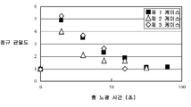
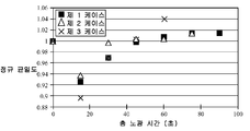
도 6 및 도 7에는, 도 1 내지 도 5를 참조하여 전술한 바와 같은 패널(12)의 실질적으로 평면형 부분에 대해, 지속 시간이 통상의 단일 노광 공정의 지속 시간보다 짧은 노광 공정을 복수 회 시행한 경우의, 세 개의 상이한 시료, 즉, 제 1 케이스 내지 제 3 케이스에 대한 결과치가 예시되어 있다. 각각의 그래프에서, X-축은 총 노광 시간을 나타내는 반면, Y-축은 도 6의 경우 정규 균일도(normalized uniformity)를 나타내고, 도 7의 경우 정규 직경(normalized diameter)을 나타낸다.6 and 7, for a substantially planar portion of the
각각의 제 1 내지 제 3 시험 케이스에 대하여, 마이크로 홀(30)을 충전 재료(50)를 이용하여 막은 후 그리고 충전 재료(50)가 유동 가능한 상태에 있는 동안에, 마이크로 홀(30)로부터 방출되는 광(즉, 스폿)의 평균 광도 초기 값을 코스메틱 표면(18)에서 측정하였다. 이 광도 값은 코스메틱 표면(18)으로부터 고정된 거리에서 통상의 광도계를 사용하여 그레이-스케일(grey-scale) 값으로서 측정하였다. 평균 값을 초과하는 플럭스 표준 편차에 100을 곱하여 방출 광의 균일도를 산출하였다. 시간(0)에서의 각각의 값을 사용하여 각각의 케이스에 대한 측정치 정규 값을 구하였다. 이에 따라, 도 6에 도시된 바와 같이, 각각의 케이스의 시간(0)에서의 정규 균일도는 1이다.For each of the first to third test cases, the
마찬가지로, 각각의 제 1 내지 제 3 시험 케이스에 대하여, 마이크로 홀(30)을 충전 재료(50)를 이용하여 막은 후 그리고 충전 재료(50)가 유동 가능한 상태에 있는 동안에 마이크로 홀(30)로부터 방출되는 광(즉, 스폿)의 평균 직경 초기 값을 코스메틱 표면(18)에서 측정하였다. 이 직경 값은 코스메틱 표면(18)으로부터 고정된 거리에서 2차원 이미지 센서를 사용하여 촬영한 영상을 사용하여 측정하였다. 모든 마이크로 홀(30)의 광 스폿의 평균 값을 각각의 케이스의 직경으로 하였다. 시간(0)에서의 각각의 평균 값을 사용하여 각각의 케이스의 측정치 정규 값을 구하였다. 이에 따라, 도 7에 도시된 바와 같이, 각각의 케이스의 시간(0)에서의 정규 직경은 1이다.Likewise, for each of the first to third test cases, the
시간(0)에서의 각각의 케이스에 대한 광도 및 직경을 측정한 후, 충전 재료(50)의 경화를 시작하였다. 각각의 노광 공정의 지속 시간은 15초로 하였다. 각각의 노광 공정(N) 후, 값을 측정하여 총 노광 시간에 대한 플롯(plot)을 작성하였다. 각각의 노광 공정 사이 사이에 측정 데이터를 획득하기 위해 15초 내지 20초의 시간이 소요되었음에 주목하여야 한다. 도 6 및 도 7에 도시된 바와 같이, 노광 공정의 횟수(N)가 증가할수록, 광도 및 직경의 균일도도 증가하는 것이 일반적인 경향이다. 각각의 노광 공정의 시간은 통상의 처리 과정에서의 단 한 번의 노광 공정의 시간보다 짧아야 한다.After measuring the luminous intensity and diameter for each case at
도 6 및 도 7에 도시된 시험의 경우, 각각의 노광 공정에 후속하여, 소정 시간 간격 동안 충전 재료(50)를 경화 공급원, 여기서는 UV 광에 노출되지 않도록 하였다. 본 명세서에서는 이러한 간격을 휴지기라 칭하기로 한다. 또한, 본 명세서에는 노광 공정의 시작시부터 후속 휴지기의 종료시까지의 주기를 노광 사이클이라 칭하기로 한다.For the tests shown in FIGS. 6 and 7, following each exposure process, the
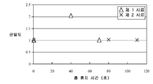
도 8 및 도 9는 총 노광 처리 시간이 동일한 두 개의 시료의 균일도 측정 결과치를 비교하여 보여주고 있다. 도 8에서는, 예를 들어, 충전 후 경화에 앞서 충전 재료(50)를 통과하여 방출된 광의 균일도가 도 6에서와 같은 노광 공정 후의 측정치의 정규 값으로서 사용되고 있다. 도 9는 도 7과 관련하여 전술한 바와 같은 직경 측정치를 보여주고 있다. 그러나, 도 9는 도 7에서의 정규 평균 직경 대신 각각의 측정 지점에서의 실제 평균 직경을 나타낸 플롯이다.8 and 9 show the uniformity measurement results of two samples having the same total exposure treatment time. In FIG. 8, for example, the uniformity of light emitted through the filling
도 8 및 도 9에서, 제 1 시료의 경우에 15초씩 네 번의 노광 주기에 이어 대략 30초의 휴지기를 가졌다. 30초가 지난 시점에 방출 광의 강도와 직경을 측정하였다. 도 8에는 네 번의 노광 주기 각각의 이후에 산출된 정규 균일도가 제 2 시료의 정규 균일도와 비교하여 도시되어 있다. 여기서, 제 2 시료는 45초에 걸친 단 한 번의 노광 주기에 이어 대략 30초의 휴지기를 거쳐 얻어진 것이다. 마찬가지로, 도 9에는 네 번의 노광 주기 각각의 이후에 산출된 제 1 시료의 평균 직경이, 45초에 걸친 단 한 번의 노광 주기에 이어 대략 30초의 휴지기를 거쳐 얻어진 제 2 시료의 평균 직경과 비교하여 도시되어 있다. 도시된 바로부터 알 수 있는 바와 같이, 휴지기를 포함함으로써 동일한 노광 처리 시간에 걸쳐 방출된 광의 균일도가 보다 증가하게 된다. 또한, 도 5와 도 8을 비교하여 알 수 있는 바와 같이, 휴지기가 길어질수록, 방출 광이 비교적 균일한 광도에 도달하기 위해 필요한 노광 공정의 횟수가 감소하였음에 주목하여야 한다. 도 6과 도 9를 비교한 경우에도 유사한 결과를 확인할 수 있다. 다시 말해, 휴지기가 길어질수록, 비교적 균일한 직경에 도달하기 위해 필요한 노광 공정의 횟수가 감소하였다. 또한, 네 번째 노광 주기 수행 결과로부터 알 수 있듯이, 추가적인 균일도 개선 효과가 최소화되는 지점이 있다. 이러한 지점을 중합 반응 공정이 포화 상태에 도달한 지점으로 특징 지을 수 있다.In FIGS. 8 and 9, the first sample had a period of approximately 30 seconds followed by four exposure cycles of 15 seconds each. At the end of 30 seconds, the intensity and diameter of the emitted light were measured. 8 shows the normal uniformity calculated after each of the four exposure cycles compared to the normal uniformity of the second sample. Here, the second sample is obtained after a single exposure period over 45 seconds followed by a pause of approximately 30 seconds. Similarly, in FIG. 9, the average diameter of the first sample calculated after each of the four exposure cycles is compared with the average diameter of the second sample obtained through the resting period of approximately 30 seconds following only one exposure cycle over 45 seconds. Is shown. As can be seen from the illustration, the inclusion of the resting period further increases the uniformity of the emitted light over the same exposure treatment time. In addition, as can be seen by comparing FIG. 5 and FIG. 8, it should be noted that as the rest period becomes longer, the number of exposure steps required for the emitted light to reach a relatively uniform luminous intensity decreases. Similar results can be seen when comparing FIG. 6 and FIG. 9. In other words, the longer the resting period, the fewer the number of exposure processes required to reach a relatively uniform diameter. In addition, as can be seen from the result of performing the fourth exposure cycle, there is a point where the additional uniformity improvement effect is minimized. This point may be characterized as the point where the polymerization reaction reaches saturation.
도 8 및 도 9에 도시된 바와 같이, 초기에 45초의 단 한 번의 노광 공정을 거친 제 2 시료에 대하여 시험 지점을 약간 더 추가하였다. 이러한 후속 시험 지점 각각에 있어서, 노광 사이클은, 제 1 시료의 시험에서와 마찬가지로, 15초의 노광 주기와 대략 30초의 휴지기로 이루어지도록 하였다. 이러한 추가적인 시험 지점은 또한, 전술한 포화 상태를 입증할 뿐만 아니라, 적어도 한 번의 휴지기에 후속하여 다른 한 번의 노광 주기가 수행된 이후 달성되는 급격한 균일도 개선 효과를 입증하고 있다.As shown in Figures 8 and 9, slightly more test points were added for the second sample, which initially went through only one exposure process of 45 seconds. At each of these subsequent test points, the exposure cycle was made to consist of an exposure period of 15 seconds and a pause of approximately 30 seconds, as in the test of the first sample. This additional test point also not only demonstrates the saturation described above, but also demonstrates the rapid uniformity improvement effect achieved after another exposure cycle is performed following at least one pause.
도 10은 노광 공정 시행 횟수와 총 노광 시간은 동일하지만 휴지기가 상이한 경우의 두 개의 시료의 결과치를 비교하여 보여주고 있다. 각각의 시료에 대하여, 최초 노광 공정 횟수(N)는 다섯 번으로 하였으며 노광 시간은 15초로 하였다. 제 1 시료의 경우에는 휴지기를 10초로 하였다. 제 2 시료의 경우에는 휴지기를 20초로 하였다. 총 휴지 시간 대비 코스메틱 표면(18)으로부터 방출되는 광의 정규 균일도를 나타낸 그래프로부터 알 수 있는 바와 같이, 휴지기의 시간이 증가할수록 균일도가 증가한다. 제 2 시료의 경우 노광 사이클을 추가하여도 균일도에는 변화가 없는 반면, 제 1 시료의 경우 노광 사이클을 추가함에 따라 추가적인 균일도 개선 효과를 초래한다.FIG. 10 shows a comparison of the results of two samples when the number of exposure steps and the total exposure time are the same but the resting periods are different. For each sample, the initial exposure process number N was five and the exposure time was 15 seconds. In the case of the first sample, the resting period was 10 seconds. In the case of the second sample, the resting period was 20 seconds. As can be seen from a graph showing the normal uniformity of light emitted from the
종합적으로, 도 5 내지 도 10에서 입증되고 있는 바와 같이, 결과적으로 얻어지는 균일도와 관련하여서는 각각의 노광 사이클의 휴지기의 길이가 사이클의 노광 시간보다 중요하다. 충전 재료(50)에 대한 휴지기의 최대치가 존재하며, 이러한 최대치 경과 후에는 노광 사이클을 추가하여도 휴지기로 인한 균일도 개선 효과는 없다. 또한, 휴지기의 최소치도 존재하는데, 이러한 최소치 아래에서는 소망하는 균일도 개선 효과를 달성할 수 있을 정도로 충전 재료(50)를 충분히 냉각할 수 없다. 이러한 최대치 및 최소치는 충전 재료(50)의 함량, 마이크로 홀(30)의 치수, 충전 재료(50)를 경화하도록 사용되는 공급원의 특성, 각각의 노광 사이클의 길이 등에 따라 결정된다. 이에 따라, 휴지기의 최대치 및 최소치는 전술한 예에서와 유사한 방식으로 실험적으로 결정될 수 있다.Overall, as demonstrated in FIGS. 5-10, the length of the rest period of each exposure cycle is more important than the exposure time of the cycle with respect to the resulting uniformity. There is a maximum value of the resting period for the filling
간략하게 전술한 바와 같이, 적당한 광 투과성 재료는 유동 가능한 상태로 마이크로 홀(30)의 내부에 배치될 수 있는 폴리머 재료이며, 제자리에서 적당한 중합 반응(들)이 이루어질 수 있다. 이러한 중합 반응(들)에는, 전술한 바와 같은 가시광 투과 능력 및/또는 실질적으로 투명하게 보일 수 있는 성질 등과 같은 적당한 광학적 투과 특성을 갖춘 폴리머 재료를 생성하는 적당한 반응이 포함될 수도 있다. 보통 채용되고 있는 중합 반응으로는, 방사선 가교 결합 및/또는 광화학적으로 야기되는 가교 결합을 포함하는 적어도 하나의 중합 공정이 있다.As briefly described above, a suitable light transmissive material is a polymeric material that can be disposed within the micro-holes 30 in a flowable state, and suitable polymerization reaction (s) can be made in place. Such polymerization reaction (s) may include suitable reactions to produce polymeric materials with suitable optical transmission properties, such as the visible light transmission capabilities and / or properties that may appear substantially transparent as described above. Polymerization reactions which are usually employed include at least one polymerization process including radiation crosslinking and / or photochemically induced crosslinking.
상세히 전술한 바와 같은 다양한 실시예에 있어서, 채용되고 있는 중합 공정은 광에 의해 야기되는 가교 결합이다. 소정의 특정 실시예에 있어서, 이러한 광에 의해 야기되는 가교 결합은 전술한 바와 같은 UV 스펙트럼의 광을 사용하는 것으로 고려된다. 궁극적으로 마이크로 홀(30)에 존재하는 광 투과성 폴리머 재료는 적당한 에폭시 아크릴레이트 올리고머와 조합하여 적당한 고리형 및 선형 지방족 에스테르를 포함하는 조성물로부터 UV 광에 의해 광 개시되었던 재료이다. 시작 재료는 필요한 경우 적당한 광 개시제 뿐만 아니라 다양한 반응 조절제 및 개질제를 포함할 수 있다. 이러한 재료는 중합 반응의 결과물로서 완전히 또는 부분적으로 소비될 수도 있다.In various embodiments as detailed above, the polymerization process employed is a crosslinking caused by light. In certain specific embodiments, the crosslinks caused by such light are contemplated to use light in the UV spectrum as described above. The light transmissive polymeric material that is ultimately present in the
특정 실시예에 있어서, 마이크로 홀(30)에 존재하는 경화된 중합 반응을 거친 재료는 재료가 UV 광원(26)에 의해 일시적으로 노광 처리되는 공정에 의해 중합이 일어나는 것으로 고려된다. 전술한 바와 같이, 이와 같이 채용되는 일시적인 노광 공정은 UV 노광 주기, 휴지기 및 제 2 UV 노광 주기로 이루어지는 적어도 한 번의 노광 간격을 포함한다. 휴지기와 UV 노광 공정이 번갈아 여러 번 반복적으로 또는 주기적으로 수행될 수 있는 것으로 고려된다. 소정의 용례에 있어서, 폴리머 재료는 15초 내지 30초 동안 UV 노광 공정을 거친 후, 15초 내지 30초 동안 UV 노광이 이루어지지 않는 휴지기를 가지며, 이후 다시 15초 내지 30초 동안 제 2 UV 노광 공정을 거친다. 지속 시간이, 예를 들어, 5초 정도로 짧은 휴지기와 노광 공정이 또한 가능하지만, 이 경우에는 보다 많은 용례를 필요로 할 수도 있다. 특히 UV 광원(26)이 UV LED 조명 장치인 경우에는, 반복 횟수가 많은 모드가 가능하다.In certain embodiments, the cured polymerized material present in the
본 명세서에는 패널이 대략적으로만 설명되어 있다. 패널의 실질적으로 평면형의 부분은 제 1 평면형 표면과, 이 제 1 평면형 표면의 반대쪽 제 2 평면형 표면을 포함한다. 복수 개의 마이크로 홀이 제 1 평면형 표면으로부터 제 2 평면형 표면으로 관통 형성되어 있으며, 각각의 마이크로 홀은 개개의 평면형 표면에 형성되어 있는 제 1 및 제 2 개구와 연통하여 이들 개구의 사이에 내면을 구비한다. 각각의 마이크로 홀의 내부에는 광 투과성 폴리머 재료가 배치되며, 이러한 폴리머 재료는 몸체의 제 1 평면형 표면과 실질적으로 동일 평면 상의 제 1 외면과, 이 제 1 외면의 반대쪽 제 2 외면, 그리고 이들 외면 사이에 마련되는 중심 몸체를 포함한다. 광 투과성 폴리머 재료의 중심 몸체는 개개의 마이크로 홀의 내면과 접촉 결합되는 중앙의 외면을 구비한다.The panel is only outlined here. The substantially planar portion of the panel includes a first planar surface and a second planar surface opposite the first planar surface. A plurality of micro holes are formed penetrating from the first planar surface to the second planar surface, each micro hole having an inner surface therebetween in communication with the first and second openings formed in the respective planar surfaces. do. Inside each micro hole is a light transmissive polymer material disposed between the first outer surface substantially coplanar with the first planar surface of the body, and between the second outer surface opposite the first outer surface, and between these outer surfaces. And a central body provided. The central body of the light transmissive polymeric material has a central outer surface that is in contact with the inner surface of the individual micro holes.
일 실시예에서 사용되고 있는 광 투과성 폴리머 재료는 적어도 두 번의 별개의 간격으로 수행되는 UV 노광 공정을 거쳐 UV 경화 가능한 에폭시 아크릴레이트 올리고머로부터 유도되는 적어도 5%의 반복 단위를 갖는 재료이다. 즉, 일 실시예의 광 투과성 폴리머 재료는, 성분 중 적어도 5%가 적어도 두 번의 간격에 걸쳐 UV 노광 공정을 거친 UV 경화 가능한 에폭시 아크릴레이트 올리고머로부터 유도되는, 폴리머 체인을 포함한다. UV 노광 공정은 대략 365nm 내지 대략 405nm 사이의 파장을 지향할 수 있다. 각각의 노광 공정 사이사이에는 UV 노광이 이루어지지 않는 휴지기가 수행된다.The light transmissive polymer material used in one embodiment is a material having at least 5% repeat units derived from a UV curable epoxy acrylate oligomer via a UV exposure process performed at least at two separate intervals. That is, the light transmissive polymer material of one embodiment comprises a polymer chain wherein at least 5% of the components are derived from UV curable epoxy acrylate oligomers that have undergone a UV exposure process over at least two intervals. The UV exposure process can direct wavelengths between about 365 nm and about 405 nm. Between each exposure process, a rest period during which no UV exposure is performed is performed.
보다 바람직하게는, 광 투과성 폴리머 재료는 폴리머 체인 중 10%를 초과하는 양의, UV 경화 가능한 에폭시 아크릴레이트 올리고머로부터 유도되는 반복 단위를 포함하며, 폴리머 체인 중 적어도 20%가 지방족 에스테르로부터 유도되며, 폴리머 체인 중 적어도 5%가 고리형 지방족 에스테르로부터 유도된다. 광 투과성 폴리머 재료는 지방족 실란으로부터 유도되는 폴리머 체인 중 적어도 0.25%를 더 포함할 수 있다.More preferably, the light transmissive polymer material comprises repeating units derived from UV curable epoxy acrylate oligomers in an amount greater than 10% of the polymer chain, at least 20% of the polymer chain being derived from aliphatic esters, At least 5% of the polymer chains are derived from cyclic aliphatic esters. The light transmissive polymeric material may further comprise at least 0.25% of the polymer chains derived from aliphatic silanes.
중합 반응을 거친 충전 재료(50)는, 패널(12)의 마이크로 홀(30)에 의해 형성되는 패턴을 볼 수 있도록 하기 위하여, 후면(14)으로 조사된 광을 코스메틱 표면(18)의 개구를 통해 전달하는 광 통로로서 기능한다. 이에 따라, 충전 재료는 렌즈의 기능을 수행하지는 않는다. 이에 따라, 중합 반응을 거친 재료는 전달 광의 입사각이 각각의 마이크로 홀(30)에 존재하는 광 투과성 폴리머 재료의 외면을 가로질러 실질적으로 제로 값을 갖도록 배향되는 폴리머 단위를 포함함을 알 수 있다.Filled
전술한 방법으로부터 얻어지는 경화 상태의 충전 재료(50)에 의하면, 패널(12)을 통과하여 광을 전달할 수 있는 마이크로 홀(30)의 보호 효과를 달성할 수 있다. 전술한 바와 같이 휴지기를 포함한 경화 과정을 거친 광학적으로 투명한 충전 재료(50)와 마이크로 홀(30)의 사용을 통해, 도 11에 도시된 바와 같이 내측으로부터 조사되는 광이 마이크로 홀(30)을 관통하도록 함으로써, 각종 패턴의 조절된 이미지를 표시할 수 있는 육안으로 확인 가능한 평활하면서도 연속적인 패널 표면을 생성할 수 있다. 도 11에는 백라이트(70)를 포함하는 패널(12)이 도시되어 있으며, 상기 백라이트는 LED, 형광등이나 백열등, 또는 그외 다른 조명 장치일 수도 있다. 패널(12)은 보다 크기가 큰 하우징 내에 삽입되는 섹션의 형태로 형성될 수도 있으며, 또는 도 11에 도시된 바와 같이 하우징(72)의 일체형의 섹션의 형태로 형성될 수도 있다.According to the filling
패널(12)은 휴대용 전자 기기, 예를 들어, MP3 플레이어, 컴퓨터, 휴대폰, DVD 플레이어 등을 포함하는 모든 방식의 용례에 사용될 수 있다. 개시된 방법 및 패널은 발광 메시지, 이미지 또는 다른 인지 가능한 특징이나 패턴을 사용자에게 제공할 수 있는 능력을 갖춘 가시적으로 연속적이며 끊긴 부분이 없는 패널 표면이 요구되는 사실상 모든 용례에 적용 가능하다.The
본 발명이 소정의 실시예와 관련하여 설명되어 있긴 하지만, 본 발명의 방법이 개시된 실시예로만 제한되는 것은 아니며, 반대로, 다양한 변형예 및 첨부된 특허청구범위의 영역에 포함되는 등가의 단계 및 장치를 포함하는 의미로 해석되어야 함을 이해할 수 있을 것이다.Although the present invention has been described in connection with certain embodiments, the methods of the invention are not limited to the disclosed embodiments, on the contrary, the equivalent steps and apparatus falling within the scope of various modifications and appended claims. It will be understood that the meaning should be interpreted to include.
Claims (15)
일 패턴으로 배열되는 복수 개의 마이크로 홀을 광 투과성 폴리머 재료(polymeric material)를 이용하여 막는 단계로서, 상기 광 투과성 폴리머 재료는 유동 가능(workable)한 상태에 있으며, 상기 복수 개의 마이크로 홀은 상기 패널의 실질적으로 평면형 영역의 제 1 표면의 제 1 개구로부터 상기 제 1 표면의 반대쪽의 상기 실질적으로 평면형 영역의 제 2 표면의 제 2 개구까지 연장되고, 상기 제 1 개구 및 제 2 개구 각각의 직경은 상기 실질적으로 평면형 영역의 두께보다 작은, 상기 복수 개의 마이크로 홀을 막는 단계; 그리고
상기 가시광 투과성 폴리머 재료를 제 1 노광 주기 동안 공급원에 노출시키고, 상기 제 1 노광 주기 이후 상기 광 투과성 폴리머 재료가 상기 공급원에 노출되지 않는 제 1 휴지기를 제공하며, 상기 제 1 휴지기 이후 제 2 노광 주기 동안 상기 광 투과성 폴리머 재료를 상기 공급원에 노출시킴으로써, 상기 복수 개의 마이크로 홀을 막고 있는 상기 광 투과성 폴리머 재료를 유동 가능한 상태로부터 상기 광 투과성 폴리머 재료가 상기 복수 개의 마이크로 홀의 내면에 고정되는 경화 상태(set state)로 경화 처리하는 단계를 포함하는 것을 특징으로 하는 방법.As a method for manufacturing a panel,
Blocking a plurality of micro holes arranged in a pattern using a light transmissive polymer material, wherein the light transmissive polymer material is in a workable state, and the plurality of micro holes are formed in the panel. Extending from a first opening of the first surface of the substantially planar region to a second opening of the second surface of the substantially planar region opposite the first surface, the diameter of each of the first opening and the second opening being the Blocking the plurality of micro holes, which is substantially less than the thickness of the planar region; And
Exposing the visible light transmissive polymer material to a source during a first exposure period, providing a first rest period during which the light transmissive polymer material is not exposed to the source after the first exposure period, and after the first rest period a second exposure period By exposing the light transmissive polymer material to the source during the curing state in which the light transmissive polymer material is fixed to an inner surface of the plurality of micro holes from the flowable state of the light transmissive polymer material blocking the plurality of micro holes. curing) in a state).
상기 복수 개의 마이크로 홀을 막고 있는 상기 광 투과성 폴리머 재료를 유동 가능한 상태로부터 경화 상태로 경화 처리하는 단계는 상기 제 2 휴지기 이후 완료되는 것을 특징으로 하는 방법.5. The method of claim 1 or 4, further comprising providing a second rest period wherein the light transmissive polymer material is not exposed to the source after the second exposure period,
Curing the light transmissive polymer material blocking the plurality of micro holes from a flowable state to a cured state is completed after the second rest period.
상기 복수 개의 마이크로 홀을 막고 있는 상기 광 투과성 폴리머 재료를 유동 가능한 상태로부터 경화 상태로 경화 처리하는 단계는 상기 제 1 휴지기 이후 상기 제 2 노광 주기를 시작하여 상기 노광 사이클을 적어도 두 번 수행하는 단계를 포함하는 것을 특징으로 하는 방법.The method according to claim 1 or 2, wherein the first exposure period and the first rest period together form an exposure cycle,
Curing the light transmissive polymer material blocking the plurality of micro holes from a flowable state to a cured state may include performing the exposure cycle at least twice by starting the second exposure cycle after the first rest period. Method comprising a.
각각의 노광 주기 동안 상기 공급원을 동일한 위치에 유지하는 단계를 추가로 포함하는 것을 특징으로 하는 방법.3. The method of claim 1 or 2, further comprising: arranging said source to be orthogonal to said substantially planar region; And
And maintaining said source in the same position during each exposure period.
상기 제 1 평면형 표면으로부터 상기 제 2 평면형 표면으로 관통하여 형성되며, 각각 개개의 평면형 표면에 형성되는 제 1 및 제 2 개구와 연통하고, 상기 평면형 표면 사이에 내면을 구비하는 복수 개의 마이크로 홀; 그리고
각각의 마이크로 홀의 내부에 배치되며, 몸체(body)의 제 1 평면형 표면과 실질적으로 동일 평면의 제 1 외면과, 상기 제 1 외면 반대쪽의 제 2 외면, 그리고 이들 외면 사이에 배치되는 중앙 몸체(central body)를 포함하는 광 투과성 폴리머 재료를 포함하며,
상기 광 투과성 폴리머 재료의 중앙 몸체는 상기 내면과 접촉 결합하는 중앙 외면을 구비하며,
상기 광 투과성 폴리머 재료는, 성분 중 적어도 5%가, 휴지기를 사이에 두고 분리 수행되는 적어도 두 번의 UV 노광 주기에 노출된 UV 경화 가능한 에폭시 아크릴레이트 올리고머로부터 유도되는, 폴리머 체인을 포함하는 것을 특징으로 하는 패널.A substantially planar portion comprising a first planar surface and a second planar surface opposite the first planar surface;
A plurality of micro holes penetrating from said first planar surface to said second planar surface, communicating with first and second openings formed in respective planar surfaces, said plurality of micro holes having an inner surface therebetween; And
A central body disposed inside each micro hole and disposed between a first outer surface that is substantially coplanar with a first planar surface of the body, a second outer surface opposite the first outer surface, and between these outer surfaces a light transmissive polymer material comprising a body),
A central body of the light transmissive polymeric material has a central outer surface in contact with the inner surface,
The light transmissive polymeric material comprises a polymer chain, wherein at least 5% of the components are derived from UV curable epoxy acrylate oligomers exposed to at least two UV exposure cycles that are performed separately with a resting period. Panel.
Applications Claiming Priority (3)
| Application Number | Priority Date | Filing Date | Title |
|---|---|---|---|
| US12/732,851 | 2010-03-26 | ||
| US12/732,851 US8524127B2 (en) | 2010-03-26 | 2010-03-26 | Method of manufacturing a panel with occluded microholes |
| PCT/US2011/029951 WO2011119931A2 (en) | 2010-03-26 | 2011-03-25 | Method of manufacturing a panel with occluded microholes and products made thereby |
Publications (1)
| Publication Number | Publication Date |
|---|---|
| KR20130052555A true KR20130052555A (en) | 2013-05-22 |
Family
ID=44656819
Family Applications (1)
| Application Number | Title | Priority Date | Filing Date |
|---|---|---|---|
| KR1020127026686A KR20130052555A (en) | 2010-03-26 | 2011-03-25 | Method of manufacturing a panel with occluded microholes and products made thereby |
Country Status (6)
| Country | Link |
|---|---|
| US (2) | US8524127B2 (en) |
| JP (1) | JP2013527049A (en) |
| KR (1) | KR20130052555A (en) |
| CN (1) | CN102822706A (en) |
| TW (1) | TW201202600A (en) |
| WO (1) | WO2011119931A2 (en) |
Families Citing this family (9)
| Publication number | Priority date | Publication date | Assignee | Title |
|---|---|---|---|---|
| CN103313553A (en) * | 2012-03-08 | 2013-09-18 | 珠海格力电器股份有限公司 | Household appliance panel, household appliance, and processing method of household appliance panel |
| JP6020232B2 (en) * | 2013-02-14 | 2016-11-02 | フジテック株式会社 | Display device |
| CN105814623B (en) * | 2013-12-13 | 2019-12-03 | 邦&奥夫森公司 | Luminous pattern on surface |
| CN104780479A (en) * | 2014-01-11 | 2015-07-15 | 富泰华精密电子(郑州)有限公司 | Electronic device with sound passing hole and electronic device sound passing hole processing method |
| US20160349808A1 (en) * | 2015-05-29 | 2016-12-01 | Microsoft Technology Licensing, Llc | Micro-Hole Perforated Structure |
| CN108105983A (en) * | 2016-11-24 | 2018-06-01 | 美的集团股份有限公司 | Air-conditioning panel and its manufacturing method and air conditioner |
| EP3395454B1 (en) * | 2017-04-26 | 2022-11-02 | Fast & Fluid Management B.V. | Dispenser for tinting pastes |
| US20190271445A1 (en) * | 2018-03-01 | 2019-09-05 | Dell Products L.P. | System and method for producing indicator light assembly with plastic housing |
| US10821889B2 (en) | 2018-10-19 | 2020-11-03 | Shanghai Yanfeng Inqiao Automotive Trim Systems Co. Ltd. | Vehicle interior component |
Family Cites Families (34)
| Publication number | Priority date | Publication date | Assignee | Title |
|---|---|---|---|---|
| US3440388A (en) * | 1966-04-04 | 1969-04-22 | Monsanto Co | Method for machining with laser beam |
| US4155972A (en) * | 1977-09-06 | 1979-05-22 | Keystone Consolidated Industries, Inc. | Multiple-shot method of molding plastic products |
| US4716270A (en) * | 1985-11-04 | 1987-12-29 | Rockwell International Corporation | Non-contact scribing process for organic maskants on metals or alloys thereof |
| WO1992008569A1 (en) * | 1990-11-14 | 1992-05-29 | Fanuc Ltd | Optical axis adjusting method for laser robot and system therefor |
| JPH07201260A (en) | 1993-12-29 | 1995-08-04 | Yamatake Honeywell Co Ltd | Display window forming method for electronic switch |
| JPH07271309A (en) | 1994-04-01 | 1995-10-20 | Giichi Ishihara | Display plate |
| JPH08215865A (en) | 1995-02-16 | 1996-08-27 | Sumitomo Electric Ind Ltd | Fluororesin coated material and its production |
| FR2736191B1 (en) * | 1995-06-29 | 1997-09-26 | Franco Belge Combustibles | METHOD AND INSTALLATION FOR WELDING A GRID-SPACER OF A FUEL ASSEMBLY FOR A NUCLEAR REACTOR AND DEVICE FOR WELDING FROM THE INSIDE OF A GRID |
| AU3301197A (en) * | 1996-06-05 | 1998-01-05 | Larry W. Burgess | Blind via laser drilling system |
| US5718326A (en) * | 1996-07-22 | 1998-02-17 | Delco Electronics Corporation | Backlit button/switchpad assembly |
| US6424786B1 (en) * | 1996-12-02 | 2002-07-23 | Honeywell International Inc. | Illumination assembly |
| DE19717636A1 (en) * | 1997-04-25 | 1998-11-12 | Trw Fahrzeugelektrik | Method for producing a panel part, actuating part or the like parts with function symbols for the illumination with transmitted light |
| US5926293A (en) * | 1997-09-11 | 1999-07-20 | Polaroid Corporation | Holographic transflector |
| US6424876B1 (en) * | 1999-07-22 | 2002-07-23 | Advanced Micro Devices, Inc. | Statistical process control system with normalized control charting |
| WO2002006858A2 (en) * | 2000-07-18 | 2002-01-24 | Optaglio Limited | Achromatic diffractive device |
| AU2003227020A1 (en) * | 2003-02-27 | 2004-09-17 | Bang And Olufsen A/S | Metal structure with translucent region |
| US6947454B2 (en) * | 2003-06-30 | 2005-09-20 | Electro Scientific Industries, Inc. | Laser pulse picking employing controlled AOM loading |
| JP2005079385A (en) * | 2003-09-01 | 2005-03-24 | Toshiba Corp | Optical semiconductor device and optical signal input/output device |
| US8084866B2 (en) * | 2003-12-10 | 2011-12-27 | Micron Technology, Inc. | Microelectronic devices and methods for filling vias in microelectronic devices |
| CA2489941C (en) * | 2003-12-18 | 2012-08-14 | Comau S.P.A. | A method and device for laser welding |
| JP2005210103A (en) | 2003-12-26 | 2005-08-04 | Semiconductor Energy Lab Co Ltd | Laser irradiator, laser irradiating method, and method of forming crystalline semiconductor film |
| US20100193481A1 (en) * | 2004-11-29 | 2010-08-05 | Electro Scientific Industries, Inc. | Laser constructed with multiple output couplers to generate multiple output beams |
| US7884315B2 (en) * | 2006-07-11 | 2011-02-08 | Apple Inc. | Invisible, light-transmissive display system |
| CN101454143B (en) * | 2006-06-02 | 2012-10-17 | Esi电子科技工业公司 | Process for structurally thinning materials drilled with via patterns |
| US7968820B2 (en) * | 2006-06-02 | 2011-06-28 | Electro Scientific Industries, Inc. | Method of producing a panel having an area with light transmissivity |
| EP2024767A4 (en) | 2006-06-02 | 2010-08-04 | Electro Scient Ind Inc | Process for optically transparent via filling |
| US8394301B2 (en) * | 2006-06-02 | 2013-03-12 | Electro Scientific Industries, Inc. | Process for forming panel with an optically transmissive portion and products related thereto |
| KR100801535B1 (en) | 2006-12-20 | 2008-02-12 | 이상태 | Information plate and manufacturing method for appliance |
| US7817685B2 (en) * | 2007-01-26 | 2010-10-19 | Electro Scientific Industries, Inc. | Methods and systems for generating pulse trains for material processing |
| US9029731B2 (en) * | 2007-01-26 | 2015-05-12 | Electro Scientific Industries, Inc. | Methods and systems for laser processing continuously moving sheet material |
| US8481887B2 (en) * | 2007-05-03 | 2013-07-09 | Electro Scientific Industries, Inc. | Method for machining tapered micro holes |
| US8288684B2 (en) * | 2007-05-03 | 2012-10-16 | Electro Scientific Industries, Inc. | Laser micro-machining system with post-scan lens deflection |
| US8116341B2 (en) * | 2007-05-31 | 2012-02-14 | Electro Scientific Industries, Inc. | Multiple laser wavelength and pulse width process drilling |
| US20100078418A1 (en) * | 2008-09-26 | 2010-04-01 | Electro Scientific Industries, Inc. | Method of laser micro-machining stainless steel with high cosmetic quality |
-
2010
- 2010-03-26 US US12/732,851 patent/US8524127B2/en not_active Expired - Fee Related
-
2011
- 2011-03-25 KR KR1020127026686A patent/KR20130052555A/en not_active Application Discontinuation
- 2011-03-25 WO PCT/US2011/029951 patent/WO2011119931A2/en active Application Filing
- 2011-03-25 CN CN2011800156866A patent/CN102822706A/en active Pending
- 2011-03-25 JP JP2013502670A patent/JP2013527049A/en not_active Withdrawn
- 2011-03-28 TW TW100110693A patent/TW201202600A/en unknown
-
2013
- 2013-08-30 US US14/015,261 patent/US20140003067A1/en not_active Abandoned
Also Published As
| Publication number | Publication date |
|---|---|
| US20140003067A1 (en) | 2014-01-02 |
| CN102822706A (en) | 2012-12-12 |
| US8524127B2 (en) | 2013-09-03 |
| WO2011119931A3 (en) | 2012-03-01 |
| WO2011119931A2 (en) | 2011-09-29 |
| TW201202600A (en) | 2012-01-16 |
| JP2013527049A (en) | 2013-06-27 |
| US20110236645A1 (en) | 2011-09-29 |
Similar Documents
| Publication | Publication Date | Title |
|---|---|---|
| KR20130052555A (en) | Method of manufacturing a panel with occluded microholes and products made thereby | |
| US11249238B2 (en) | Optical member and method for producing same | |
| TWI530705B (en) | Light guide plate, surface light source device, transmission-type image display device, method of manufacturing light guide plate, and ultraviolet curing type ink-jet ink for light guide plate | |
| JP5199248B2 (en) | Manufacturing method of panel having light transmitting portion and panel manufactured using the method | |
| US10907055B2 (en) | Curing ultraviolet sensitive polymer materials | |
| JP2012143691A (en) | Pattern forming method and pattern forming device | |
| JP2011504607A (en) | Article having recess or projection and method for manufacturing the same | |
| JP3215095U (en) | Printing unit and printing apparatus | |
| US20120070623A1 (en) | Manufacturing method of laminated body, stamper, transfer device, laminated body, molding element, and optical element | |
| JP2011080974A (en) | Method for estimating state of ultraviolet-curing resin | |
| Guarnaccio et al. | Femtosecond laser surface texturing of polypropylene copolymer for automotive paint applications | |
| JP6021365B2 (en) | Imprint apparatus and article manufacturing method using the same | |
| JP2015210963A (en) | Manufacturing method of surface light source device, surface light source device, display device and electronic apparatus | |
| KR101555230B1 (en) | Methods of forming a fine pattern using a nanoimprint lithography | |
| JP2013083928A (en) | Method of manufacturing film with coating layer | |
| JP2010146772A (en) | Light guide plate, and method of manufacturing the same | |
| US11624856B2 (en) | Method for manufacturing anti-glare film | |
| JP2015201287A (en) | Manufacturing method of light guide plate | |
| CN112770847B (en) | Thin film manufacturing method and apparatus, and thin film | |
| JP2010185005A (en) | Method for producing foamed material | |
| JP5991215B2 (en) | Photocuring resin curing monitoring method and optical component connecting method | |
| JP5813597B2 (en) | Method for producing film with multilayer film | |
| JP4510529B2 (en) | Stereolithography method and apparatus | |
| JP4578211B2 (en) | Stereolithography method and apparatus | |
| CN101276007B (en) | Diffusing plate |
Legal Events
| Date | Code | Title | Description |
|---|---|---|---|
| WITN | Application deemed withdrawn, e.g. because no request for examination was filed or no examination fee was paid |