KR20120101136A - Apparatus and method for controlling semiconductor die warpage - Google Patents
Apparatus and method for controlling semiconductor die warpage Download PDFInfo
- Publication number
- KR20120101136A KR20120101136A KR1020127018759A KR20127018759A KR20120101136A KR 20120101136 A KR20120101136 A KR 20120101136A KR 1020127018759 A KR1020127018759 A KR 1020127018759A KR 20127018759 A KR20127018759 A KR 20127018759A KR 20120101136 A KR20120101136 A KR 20120101136A
- Authority
- KR
- South Korea
- Prior art keywords
- semiconductor die
- vias
- silicon
- die
- manufacturing
- Prior art date
Links
Images

Classifications
-
- H—ELECTRICITY
- H01—ELECTRIC ELEMENTS
- H01L—SEMICONDUCTOR DEVICES NOT COVERED BY CLASS H10
- H01L23/00—Details of semiconductor or other solid state devices
- H01L23/562—Protection against mechanical damage
-
- H—ELECTRICITY
- H01—ELECTRIC ELEMENTS
- H01L—SEMICONDUCTOR DEVICES NOT COVERED BY CLASS H10
- H01L23/00—Details of semiconductor or other solid state devices
- H01L23/48—Arrangements for conducting electric current to or from the solid state body in operation, e.g. leads, terminal arrangements ; Selection of materials therefor
-
- H—ELECTRICITY
- H01—ELECTRIC ELEMENTS
- H01L—SEMICONDUCTOR DEVICES NOT COVERED BY CLASS H10
- H01L21/00—Processes or apparatus adapted for the manufacture or treatment of semiconductor or solid state devices or of parts thereof
- H01L21/02—Manufacture or treatment of semiconductor devices or of parts thereof
- H01L21/04—Manufacture or treatment of semiconductor devices or of parts thereof the devices having at least one potential-jump barrier or surface barrier, e.g. PN junction, depletion layer or carrier concentration layer
- H01L21/18—Manufacture or treatment of semiconductor devices or of parts thereof the devices having at least one potential-jump barrier or surface barrier, e.g. PN junction, depletion layer or carrier concentration layer the devices having semiconductor bodies comprising elements of Group IV of the Periodic System or AIIIBV compounds with or without impurities, e.g. doping materials
- H01L21/28—Manufacture of electrodes on semiconductor bodies using processes or apparatus not provided for in groups H01L21/20 - H01L21/268
-
- H—ELECTRICITY
- H01—ELECTRIC ELEMENTS
- H01L—SEMICONDUCTOR DEVICES NOT COVERED BY CLASS H10
- H01L2224/00—Indexing scheme for arrangements for connecting or disconnecting semiconductor or solid-state bodies and methods related thereto as covered by H01L24/00
- H01L2224/01—Means for bonding being attached to, or being formed on, the surface to be connected, e.g. chip-to-package, die-attach, "first-level" interconnects; Manufacturing methods related thereto
- H01L2224/10—Bump connectors; Manufacturing methods related thereto
- H01L2224/15—Structure, shape, material or disposition of the bump connectors after the connecting process
- H01L2224/16—Structure, shape, material or disposition of the bump connectors after the connecting process of an individual bump connector
- H01L2224/161—Disposition
- H01L2224/16151—Disposition the bump connector connecting between a semiconductor or solid-state body and an item not being a semiconductor or solid-state body, e.g. chip-to-substrate, chip-to-passive
- H01L2224/16221—Disposition the bump connector connecting between a semiconductor or solid-state body and an item not being a semiconductor or solid-state body, e.g. chip-to-substrate, chip-to-passive the body and the item being stacked
- H01L2224/16225—Disposition the bump connector connecting between a semiconductor or solid-state body and an item not being a semiconductor or solid-state body, e.g. chip-to-substrate, chip-to-passive the body and the item being stacked the item being non-metallic, e.g. insulating substrate with or without metallisation
-
- H—ELECTRICITY
- H01—ELECTRIC ELEMENTS
- H01L—SEMICONDUCTOR DEVICES NOT COVERED BY CLASS H10
- H01L23/00—Details of semiconductor or other solid state devices
- H01L23/28—Encapsulations, e.g. encapsulating layers, coatings, e.g. for protection
- H01L23/31—Encapsulations, e.g. encapsulating layers, coatings, e.g. for protection characterised by the arrangement or shape
- H01L23/3107—Encapsulations, e.g. encapsulating layers, coatings, e.g. for protection characterised by the arrangement or shape the device being completely enclosed
- H01L23/3121—Encapsulations, e.g. encapsulating layers, coatings, e.g. for protection characterised by the arrangement or shape the device being completely enclosed a substrate forming part of the encapsulation
- H01L23/3128—Encapsulations, e.g. encapsulating layers, coatings, e.g. for protection characterised by the arrangement or shape the device being completely enclosed a substrate forming part of the encapsulation the substrate having spherical bumps for external connection
-
- H—ELECTRICITY
- H01—ELECTRIC ELEMENTS
- H01L—SEMICONDUCTOR DEVICES NOT COVERED BY CLASS H10
- H01L23/00—Details of semiconductor or other solid state devices
- H01L23/34—Arrangements for cooling, heating, ventilating or temperature compensation ; Temperature sensing arrangements
- H01L23/36—Selection of materials, or shaping, to facilitate cooling or heating, e.g. heatsinks
- H01L23/367—Cooling facilitated by shape of device
- H01L23/3677—Wire-like or pin-like cooling fins or heat sinks
-
- H—ELECTRICITY
- H01—ELECTRIC ELEMENTS
- H01L—SEMICONDUCTOR DEVICES NOT COVERED BY CLASS H10
- H01L23/00—Details of semiconductor or other solid state devices
- H01L23/48—Arrangements for conducting electric current to or from the solid state body in operation, e.g. leads, terminal arrangements ; Selection of materials therefor
- H01L23/481—Internal lead connections, e.g. via connections, feedthrough structures
-
- H—ELECTRICITY
- H01—ELECTRIC ELEMENTS
- H01L—SEMICONDUCTOR DEVICES NOT COVERED BY CLASS H10
- H01L2924/00—Indexing scheme for arrangements or methods for connecting or disconnecting semiconductor or solid-state bodies as covered by H01L24/00
- H01L2924/15—Details of package parts other than the semiconductor or other solid state devices to be connected
- H01L2924/151—Die mounting substrate
- H01L2924/153—Connection portion
- H01L2924/1531—Connection portion the connection portion being formed only on the surface of the substrate opposite to the die mounting surface
- H01L2924/15311—Connection portion the connection portion being formed only on the surface of the substrate opposite to the die mounting surface being a ball array, e.g. BGA
Landscapes
- Engineering & Computer Science (AREA)
- Physics & Mathematics (AREA)
- Condensed Matter Physics & Semiconductors (AREA)
- General Physics & Mathematics (AREA)
- Computer Hardware Design (AREA)
- Microelectronics & Electronic Packaging (AREA)
- Power Engineering (AREA)
- Manufacturing & Machinery (AREA)
- Internal Circuitry In Semiconductor Integrated Circuit Devices (AREA)
- Design And Manufacture Of Integrated Circuits (AREA)
- Semiconductor Integrated Circuits (AREA)
- Lead Frames For Integrated Circuits (AREA)
Abstract
반도체 다이는 뒤틀림을 감소시키도록 배열된 실리콘 관통 비아들을 가진다. 실리콘 관통 비아들은 반도체 다이의 열 팽창 계수를 조정하며, 기판 변형을 허용하고, 또한 잔여 응력을 완화시킨다. 실리콘 관통 비아들은 반도체 다이의 에지들 및/또는 코너들에 위치될 수 있다. 실리콘 관통 비아들은 반도체 다이의 뒤틀림을 감소시키기 위해서 라운드 코너 비아들로 보충될 수 있는 응력 완화 비아들이다.The semiconductor die has silicon through vias arranged to reduce distortion. Silicon through vias adjust the coefficient of thermal expansion of the semiconductor die, allow substrate deformation, and also relieve residual stress. Silicon through vias may be located at the edges and / or corners of the semiconductor die. Silicon through vias are stress relief vias that can be supplemented with round corner vias to reduce warping of the semiconductor die.
Description
본 개시는 일반적으로 반도체 다이 제조에 관한 것이다. 보다 상세하게는, 본 개시는 반도체 다이들을 제조하는 동안 뒤틀림(warpage)을 제어하는 것에 관한 것이다.The present disclosure generally relates to semiconductor die fabrication. More specifically, the present disclosure relates to controlling warpage during fabrication of semiconductor dies.
반도체 웨이퍼들 및 다이들에서의 잔류 응력은 뒤틀림을 야기한다. 예를 들어, 웨이퍼 상에 (예컨대, 트랜지스터들을 생성하기 위해서) 증착된 물질들은 불균형 응력을 초래하는, 기판과 상이한 응력을 가지도록 엔지니어링(engineer)될 수 있다. 다른 경우들에서, 응력들은 엔지니어링되는 것이 아니라, 단지 상이한 물질들로부터 발생한다. 기판과 증착된 물질들 사이의 응력은 불균형하며, 기판은 평형 응력에 도달하도록 뒤틀리거나 또는 구부려질 수 있다.Residual stress in semiconductor wafers and dies causes distortion. For example, materials deposited on a wafer (eg, to produce transistors) can be engineered to have a different stress than the substrate, resulting in an unbalanced stress. In other cases, the stresses are not engineered, but only arise from different materials. The stress between the substrate and the deposited materials is unbalanced, and the substrate can be warped or bent to reach the equilibrium stress.
또한, 패키징된 다이에 의해 경험되는 온도의 변화는 뒤틀림을 야기할 수 있다. 패키지의 열 팽창 계수(CTE)는 다이의 CTE와 상이하다. 뒤틀림은 패키지 및 다이의 물질 세트들 사이의 CTE 부정합(mismatch)의 결과로서 발생한다. 뒤틀림은 패키지와 다이 사이에 상당한 두께 차가 존재할 때 악화된다.In addition, the change in temperature experienced by the packaged die can cause distortion. The coefficient of thermal expansion (CTE) of the package is different from the CTE of the die. Warpage occurs as a result of CTE mismatch between material sets in the package and die. Warping is exacerbated when there is a significant thickness difference between the package and the die.
패키지와 다이 사이의 상당한 두께 차를 가지는 제품의 일례는 적층된 IC이다. 얇은 웨이퍼들은 종래에는 적층된 IC들에서 사용되어, 실리콘 관통 비아(through silicon via)들의 제조를 보조한다. 일부 경우들에서, 다이는 1mm 패키지의 두께를 변화시키지 않고 50 마이크론보다 작게 얇아질 수 있다. 상당한 두께 차의 결과로서, 심각한 뒤틀림이 발생할 수 있다.One example of a product with a significant thickness difference between the package and the die is a stacked IC. Thin wafers are conventionally used in stacked ICs to assist in the manufacture of through silicon vias. In some cases, the die may be thinner than 50 microns without changing the thickness of the 1 mm package. As a result of significant thickness differences, severe warping may occur.
뒤틀림이 심각할 때, 패키지로의 다이의 부적당한 본딩(bonding)이 발생한다. 다시 말해서, 뒤틀림은 일부 범프들 또는 기둥들이 패키지 어셈블리 프로세스 동안 기판에 부착되는 것을 막는다. 뒤틀림이 어셈블리 이후에 발생하는 경우, 범프들 또는 기둥들은 소비자가 최종 사용자 디바이스를 가지고 있을 때 분리(de-attach)될 수 있다.When the warpage is severe, improper bonding of the die into the package occurs. In other words, the distortion prevents some bumps or pillars from attaching to the substrate during the package assembly process. If warpage occurs after assembly, bumps or pillars may be present when the consumer has an end user device. It can be de-attached.
도 3에 보여지는 바와 같이, 뒤틀린 패키지 기판(310)은 중앙에서 뒤틀린 다이(320)에 커플링(couple)되지 않는다. 즉, 중앙에 위치된 상호접속부(interconnect)들(330)은 패키지 기판(310)에 접촉하지 않는다. 도시되지 않지만, 열적 부정합은 코너에서 상호접속부들(330)에 응력을 가하여, 패키지 기판(310)이 다이(320)로부터 분리되게 할 수 있다. As shown in FIG. 3, the warped
또한, 상호접속부 피로 수명(fatigue life)은 다이와 패키지 기판 사이의 열 팽창 계수(CTE)가 부정합일 때 감소한다. 온도가 변화할 때, 어셈블리는 팽창에서의 부정합을 수용하도록 구부려진다. 측정들 및 기계 모델들에 기초하여, 뒤틀림은 다이의 주변에서 특히, 코너들에서 발생하는 것으로 나타난다. 칩의 코너에 집중된 스트레인(strain)은 코너로부터 전파되는 크랙(crack)을 초래한다. 크랙이 전파됨에 따라, 칩-언더필(chip-underfill) 인터페이스 또는 다른 약한 인터페이스가 개방되어, 칩 유전체에서의 상호접속 피로 또는 전기적 손상(failure)을 야기한다.In addition, interconnect fatigue life is reduced when the coefficient of thermal expansion (CTE) between the die and the package substrate is mismatched. As the temperature changes, the assembly is bent to accommodate mismatch in expansion. Based on the measurements and mechanical models, the distortion appears to occur at the periphery of the die, especially at the corners. Strain concentrated at the corners of the chip results in cracks propagating from the corners. As the crack propagates, a chip-underfill interface or other weak interface opens, causing interconnect fatigue or electrical failure in the chip dielectric.
다이 유전체 인터페이스들을 포함하는 응력 엔지니어링 솔루션들이 존재하지만, 이러한 솔루션들은 상대적으로 복잡하며 비용이 많이 든다. 따라서, 다이의 뒤틀림을 효율적으로 제어하기 위한 필요성이 존재한다.Stress engineering solutions exist that include die dielectric interfaces, but these solutions are relatively complex and expensive. Thus, there is a need to efficiently control the warping of the die.
본 개시의 양상에 따라, 반도체 다이는 주변 영역에 위치된 실리콘 관통 비아들을 가진다. 실리콘 관통 비아들은 반도체 다이의 뒤틀림을 감소시킨다.In accordance with an aspect of the present disclosure, a semiconductor die has silicon through vias located in the peripheral region. Silicon through vias reduce warpage of the semiconductor die.
또 다른 양상에서, 반도체 다이를 제조하기 위한 방법은, 상기 다이의 뒤틀림을 감소시키기 위해서 상기 반도체 다이의 주변 영역에서 복수의 비-신호 반송 실리콘 관통 비아들을 제조하는 단계를 포함한다.In another aspect, a method for manufacturing a semiconductor die includes manufacturing a plurality of non-signal carrying silicon through vias in a peripheral region of the semiconductor die to reduce warping of the die.
또 다른 양상에서, 반도체 다이는, 상기 반도체 다이의 주변 영역에 위치된 상기 반도체 다이의 열 팽창 계수(CTE)를 증가시키기 위한 수단을 가진다. 상기 CTE 증가 수단은 상기 반도체 다이의 뒤틀림을 감소시킨다.In another aspect, the semiconductor die has means for increasing the coefficient of thermal expansion (CTE) of the semiconductor die located in the peripheral region of the semiconductor die. The CTE increasing means reduces distortion of the semiconductor die.
또 다른 양상에서, 반도체 다이를 설계하기 위한 컴퓨터화된 방법은, 다이 뒤틀림을 감소시키기 위해서 응력 완화 실리콘 관통 비아들에 대한 위치들을 결정하는 단계를 포함한다.In another aspect, a computerized method for designing a semiconductor die includes determining positions for stress relief silicon through vias to reduce die distortion.
상기 설명은 다음의 상세한 설명이 더 양호하게 이해될 수 있도록 본 발명의 특징들 및 기술적 이점들을 보다 광범위하게 약술하였다. 본 발명의 청구항들의 요지를 형성하는 추가적인 특징들 및 이점들이 이하에서 설명될 것이다. 개시되는 개념 및 특정 실시예들이 본 발명의 동일한 목적들을 수행하기 위한 다른 구조들을 변형하거나 또는 설계하기 위한 기초로서 용이하게 이용될 수 있다는 것이 당업자들에 의해 인식되어야 한다. 또한, 첨부되는 청구항들에 설명되는 바와 같이, 이러한 동등한 구조들이 본 발명의 기술로부터 벗어나지 않는다는 것이 당업자들에 의해 인지되어야 한다. 그 조직 및 동작 방법 모두에 관하여, 본 발명의 특성으로 여겨지는 신규한 특징들은 추가적인 객체들 및 이점들과 함께, 첨부한 도면들과 관련하여 고려될 때 다음의 설명으로부터 더 양호하게 이해될 것이다. 그러나, 특징들 각각은 단지 예시 및 설명을 목적으로 제공되며 본 발명의 제한들의 정의로서 의도되지 않는다는 것이 명백하게 이해될 것이다.The above description has outlined rather broadly the features and technical advantages of the present invention in order that the detailed description that follows may be better understood. Additional features and advantages will be described below that form the subject of the claims of the present invention. It should be appreciated by those skilled in the art that the conception and specific embodiments disclosed may be readily utilized as a basis for modifying or designing other structures for carrying out the same purposes of the present invention. It should also be appreciated by those skilled in the art that, as described in the appended claims, such equivalent structures do not depart from the teachings of the present invention. With respect to both its organization and method of operation, the novel features which are considered to be characteristic of the invention, together with additional objects and advantages, will be better understood from the following description when considered in connection with the accompanying drawings. However, it will be apparent that each of the features is provided for purposes of illustration and description only and is not intended as a definition of the limits of the invention.
본 발명의 더 완전한 이해를 위해서, 첨부한 도면들과 함께 취해지는 다음의 설명에 대한 참조가 이제 이루어진다.
도 1은 본 발명의 실시예가 유리하게 사용될 수 있는 예시적인 무선 통신 시스템을 도시하는 블록도이다.
도 2는 개시되는 반도체 다이의 회로 및 레이아웃 설계에 대한 설계 워크스테이션을 도시하는 블록도이다.
도 3은 뒤틀어진 반도체 다이 및 패키징 기판을 도시하는 블록도이다.
도 4는 응력 완화 비아들을 가지는 반도체 다이의 상면도를 도시하는 블록도이다.
도 5는 응력 완화 비아들 및 라운드 코너 비아(round corner via)들을 가지는 반도체 다이의 상면도를 도시하는 블록도이다.For a more complete understanding of the invention, reference is now made to the following description taken in conjunction with the accompanying drawings.
1 is a block diagram illustrating an exemplary wireless communication system in which embodiments of the present invention may be advantageously used.
2 is a block diagram illustrating a design workstation for circuit and layout design of a disclosed semiconductor die.
3 is a block diagram illustrating a warped semiconductor die and packaging substrate.
4 is a block diagram illustrating a top view of a semiconductor die with stress relief vias.
FIG. 5 is a block diagram illustrating a top view of a semiconductor die having stress relief vias and round corner vias.
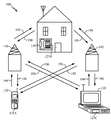
도 1은 본 개시의 실시예가 유리하게 사용될 수 있는 예시적인 무선 통신 시스템(100)을 도시하는 블록도이다. 예시를 목적으로, 도 1은 3개의 원격 유닛들(120, 130 및 150) 및 2개의 기지국들(140)을 도시한다. 무선 통신 시스템들은 더욱 많은 원격 유닛들 및 기지국들을 가질 수 있다는 것이 인지될 것이다. 원격 유닛들(120, 130 및 150)은 개시되는 반도체 다이를 포함하는 IC 디바이스들(125A, 125B 및 125C)을 포함한다. 기지국들, 스위칭 디바이스들 및 네트워크 장비를 포함하는, IC를 포함하는 임의의 디바이스는 또한 본 명세서에 개시되는 다이를 포함할 수 있다는 것이 인지될 것이다. 도 1은 기지국(140)으로부터 원격 유닛들(120, 130 및 150)로의 순방향 링크 신호들(180) 및 원격 유닛들(120, 130 및 150)로부터 기지국들(140)로의 역방향 링크 신호들(190)을 도시한다.1 is a block diagram illustrating an example
도 1에서, 무선 로컬 루프 시스템에서, 원격 유닛(120)은 모바일 전화로서 도시되고, 원격 유닛(130)은 휴대용 컴퓨터로서 도시되며, 원격 유닛(150)은 고정 위치 원격 유닛으로서 도시된다. 예를 들어, 원격 유닛들은 모바일 전화들, 핸드-헬드 개인용 통신 시스템(PCS) 유닛들, 개인용 데이터 보조기들과 같은 휴대용 데이터 유닛들, GPS 가능한 디바이스들, 내비게이션 디바이스들, 셋탑 박스들, 음악 재생기들, 비디오 재생기들, 엔터테인먼트 유닛들, 미터 판독 장비와 같은 고정 위치 데이터 유닛들, 또는 데이터 또는 컴퓨터 명령들 또는 이들의 임의의 결합을 저장하거나 또는 리트리브(retrieve)하는 임의의 다른 디바이스일 수 있다. 도 1은 본 개시의 교시들에 따라 원격 유닛들을 도시하지만, 본 개시는 이러한 예시적인 도시된 유닛들에 제한되지 않는다. 본 개시의 실시예들은 집적 회로를 포함하는 임의의 디바이스에서 적합하게 사용될 수 있다.In FIG. 1, in a wireless local loop system,
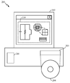
도 2는 개시되는 반도체 집적 회로의 회로 및 레이아웃 설계에 대한 설계 워크스테이션을 도시하는 블록도이다. 설계 워크스테이션(200)은 운영 체제 소프트웨어, 지원 파일들, 및 Cadence 또는 OrCAD와 같은 설계 소프트웨어를 포함하는 하드 디스크(201)를 포함한다. 또한, 설계 워크스테이션(200)은 회로 및 레이아웃(210)의 설계를 용이하게 하기 위해서 디스플레이를 포함한다. 아래에서 개시되는 바와 같이, 회로 및 레이아웃(210)은 비아 구성을 포함할 수 있다. 회로 및 레이아웃 설계(210)를 실체적으로(tangibly) 저장하기 위한 저장 매체(204)가 제공된다. 회로 및 레이아웃 설계(210)는 GDSII 또는 GERBER와 같은 파일 포맷으로 저장 매체(204) 상에 저장될 수 있다. 저장 매체(204)는 CD-ROM, DVD, 하드 디스크, 플래쉬 메모리 또는 다른 적절한 디바이스일 수 있다. 또한, 설계 워크스테이션(200)은 저장 매체(204)로부터 입력을 수용하거나 또는 저장 매체(204)에 출력을 기록하기 위한 드라이브 장치(203)를 포함한다.2 is a block diagram illustrating a design workstation for circuit and layout design of the disclosed semiconductor integrated circuit.
저장 매체(204) 상에 기록된 데이터는 로직 회로 구성들, 포토리소그래피 마스크들에 대한 패턴 데이터, 또는 전자 빔 리소그래피와 같은 직렬 기록 툴들에 대한 마스크 패턴 데이터를 특정할 수 있다. 데이터는 로직 시뮬레이션들과 연관된 타이밍도들 또는 네트 회로들과 같은 로직 검증 데이터를 더 포함할 수 있다. 저장 매체(204) 상에 데이터를 제공하는 것은 반도체 IC들을 설계하기 위한 프로세스들의 수를 감소시킴으로써 회로 및 레이아웃(210)의 설계를 용이하게 한다.The data recorded on the
본 개시에 따라, 도전성 충진물(conductive fill)(예를 들어,금속)을 가지는 실리콘 관통 비아들은 뒤틀림을 제어하기 위해서 반도체 다이(또는 웨이퍼) 내에서 제조된다. 실리콘 관통 비아들은 다이/기판 열 팽창 계수(CTE) 정합을 향상시킨다. 따라서, 상호접속부의 피로 수명 및 신뢰도는 증가한다.In accordance with the present disclosure, through-silicon vias having a conductive fill (eg, metal) are fabricated in a semiconductor die (or wafer) to control distortion. Silicon through vias improve die / substrate thermal expansion coefficient (CTE) matching. Thus, the fatigue life and reliability of the interconnects increases.
더욱이, 실리콘 관통 비아들은 잔여 응력을 완화시키며, 변형시키기 위한 기판에 대한 더 많은 공간을 생성하여, 뒤틀림이 완화되게 한다. 일 실시예에서, 실리콘 관통 비아들은 다이의 주변에 제공되는 응력 완화 비아들 및 라운드 코너 비아들이다.Moreover, through-silicon vias relieve residual stress and create more space for the substrate to deform, allowing warping to be alleviated. In one embodiment, the through silicon vias are stress relief vias and round corner vias provided around the die.
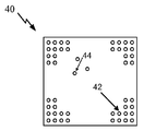
도 4에 보여지는 바와 같이, 다이(40)는 응력 완화 비아들(42)을 포함한다. 응력 완화 비아들은 뒤틀림을 제어하고 또한 잔여 응력을 릴리스(release)하기 위해서 다이 코너 주변에 배치되는 실리콘 관통 비아들이다. 또한, 응력 완화 비아들(44)은 잔여 응력을 재분배하기 위해서 중앙에 배치될 수 있다. 응력 완화 비아들(44)은 설계 파라미터들을 충족시키기 위해서 다이(40)의 임계 기능 블록들의 응력을 감소시키거나 또는 증가시키는 것을 보조할 수 있다.As shown in FIG. 4, die 40 includes
일 양상에서, 응력 완화 비아들(42)은 금속으로 채워져, 열 팽창 계수(CTE) 부정합을 향상시키는 것을 보조한다. 예시적인 비-제한 충진 물질들은 구리 및 텅스텐을 포함한다. 적절한 충진 물질의 선택은 원하는 패키지 성능 및 비용에 의존한다. 텅스텐은 더 큰 모듈러스(modulus)를 가지지만, 더 작은 열 팽창 계수(CTE)를 가진다. 예를 들어, 적층된 다이(2개의 계층) 패키지에서, 텅스텐 충진 물질은 비아들에서 더 낮은 응력을 초래하며, 적층물의 계층들 사이의 다이 대 다이 상호접속부들에서 더 높은 응력을 초래한다. 따라서, 충진 물질을 선택할 때 비아들과 상호접속부들 사이에 성능 트레이드 오프가 존재한다.In one aspect, the
일 실시예에서, 응력 완화 비아들(42, 44)은 신호들을 반송(carry)하지 않는다. 그러나, 또 다른 실시예에서, 응력 완화 비아들(42, 44)은 신호들을 반송한다.In one embodiment, the
응력 완화 비아들(42, 44)의 수 및 정확한 위치들은, 특히, 다이 크기, 비아 지름 및 응력 완화 비아의 충진 물질에 기초하여 다이마다 변경된다. 응력 완화 비아들(42, 44)의 원하는 수 및 응력 완화 비아들(44)의 위치들은 다이(40)의 열 기계 모델을 분석함으로써 반도체 다이 설계 단계 동안 계산될 수 있다. 다이의 코너에 응력 완화 비아들(42)을 위치시키는 하나의 이점은 이 영역이 다이(40)의 기능적 비아들에 대하여 종종 사용되지 않는다는 점이다. The number and exact positions of the
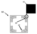
도 5에 보여지는 바와 같이, 다이(50)는 응력 완화 비아들(42)에 더하여 라운드 코너 비아들(55)을 포함한다. 일 실시예에서, 응력 완화 비아들(42)은 응력 완화를 위한 1차 메커니즘이다. 응력 완화 비아들이 자발적으로 응력을 완화시키기에 불충분한 경우, 라운드 코너 비아들(55)이 2차 메커니즘으로서 사용된다. 또 다른 실시예에서, 라운드 코너 비아들(55)은 1차 메커니즘이다.As shown in FIG. 5, die 50 includes round corner vias 55 in addition to
또한, 라운드 코너 비아들(55)은 다이(50)의 열 팽창 계수를 증가시키는 것을 보조하기 위해서 금속으로 채워질 수 있다. 다이(50)의 열 팽창 계수를 증가시킴으로써, 다이(50)의 열 팽창 계수는 패키지(미도시됨)의 열 팽창 계수와 더 양호하게 정합하여, 뒤틀림이 감소되게 할 것이다. 더욱이, 추가적인 다이 컷 아웃 영역(cut out area)은 기판 변형을 위한 더 많은 룸(room)을 생성하며, 잔여 응력을 완화시킨다.In addition, the
라운드 코너 비아(55)의 포맷은 변경될 수 있다. 일 실시예에서, 줌 뷰(zoom view)에 보여지는 바와 같이, 포맷은 실리콘 관통 비아들의 어레이이다.The format of the round corner vias 55 can be changed. In one embodiment, as shown in the zoom view, the format is an array of silicon through vias.
라운드 코너 비아들(55) 및 응력 완화 비아들(42)의 특정 배열은 열 기계 모델링 및 예상된 뒤틀림의 양에 기초하여 결정될 수 있다. 뒤틀림이 더 상당한 경우, 라운드 코너 비아들(55)이 제공되어(이는 라운드 코너 비아들(55)이 응력 완화 비아들(42)보다 더 많은 다이 물질을 제거하기 때문임), 다이(50)에 변형시키기 위한 더 많은 공간이 주어질 수 있다. 일반적인 경험 법칙(rule of thumb)에 따라, 비아 영역 대 다이 영역 비가 증가하는 경우, 뒤틀림이 더 많이 제어된다. 다시 말해서, 더 많은 다이 물질을 제거하는 것은 뒤틀림을 더 양호하게 제어한다.The particular arrangement of
일 실시예에서, 다이(50)의 기능에 대하여 사용되지 않는 영역은 응력 완화 비아들(42, 44) 및 라운드 코너 비아들(55)을 어디에 위치시키는지에 대한 결정에 영향을 미친다. 대안적으로, 뒤틀림 문제가 더 중요해질 때, 다이(50)의 기능적 블록들은 응력 완화 비아들(42, 44) 및 라운드 코너 비아들(55)을 수용하도록 설계된다.In one embodiment, the unused area for the function of the die 50 influences the determination of where to place the
응력 완화 비아들(42, 44) 및 라운드 코너 비아들(55)은 종래의 실리콘 관통 비아 형성 프로세스 동안 제조될 수 있다. 따라서, 어떠한 추가적인 제조 프로세스들도 요구되지 않는다. 더욱이, 응력 완화 비아들(42, 44) 및 라운드 코너 비아들(55)은 용이하게 제조되기 때문에, 어떠한 가외의 제조 비용들도 거의 추가되지 않는다. 최종적으로, 응력 완화 비아들(42, 44) 및 라운드 코너 비아들(55)은 CTE 부정합을 감소시킴으로써 패키지 기판/다이 상호접속부들의 신뢰도를 개선시킨다. 즉, 상호접속부 피로 수명이 증가한다.
"실리콘 관통 비아"라는 용어는 실리콘이라는 단어를 포함하지만, 실리콘 관통 비아들은 반드시 실리콘으로 구성되는 것이 아니라는 점에 유의하여야 한다. 오히려, 물질은 임의의 디바이스 기판 물질일 수 있다.Although the term "silicon through via" includes the word silicon, it should be noted that silicon through vias are not necessarily composed of silicon. Rather, the material may be any device substrate material.
본 발명 및 그 이점들이 상세하게 설명되었지만, 다양한 변경들, 치환들 및 대안들이 첨부된 청구항들에 의해 정의되는 바와 같은 본 발명의 기술로부터 벗어나지 않고 본 명세서에서 이루어질 수 있다는 것이 이해되어야 한다. 더욱이, 본 출원의 범위는 명세서에 설명된 프로세스, 기계, 제조, 물질의 구성, 수단, 방법들 및 단계들의 특정 실시예들에 제한되는 것으로 의도되지 않는다. 당업자가 본 개시로부터 용이하게 인식할 바와 같이, 본 명세서에 설명된 대응하는 실시예들과 실질적으로 동일한 기능을 수행하거나 또는 실질적으로 동일한 결과를 달성하는 현재 존재하거나 또는 추후에 개발될 프로세스들, 기계들, 제조, 물질의 구성들, 수단, 방법들 또는 단계들이 본 발명에 따라 이용될 수 있다. 따라서, 첨부된 청구항들은 이러한 프로세스들, 기계들, 제조, 물질의 구성들, 수단, 방법들 또는 단계들을 그 범위 내에 포함하는 것으로 의도된다.Although the invention and its advantages have been described in detail, it should be understood that various changes, substitutions and alterations can be made herein without departing from the spirit of the invention as defined by the appended claims. Moreover, the scope of the present application is not intended to be limited to the particular embodiments of the process, machine, manufacture, composition of matter, means, methods and steps described in the specification. As those skilled in the art will readily appreciate from the present disclosure, there are currently existing or later developed processes, machines that perform substantially the same function or achieve substantially the same results as the corresponding embodiments described herein. , Manufacture, compositions of matter, means, methods or steps may be used in accordance with the present invention. Accordingly, the appended claims are intended to include within their scope such processes, machines, manufacture, compositions of matter, means, methods or steps.
Claims (19)
상기 반도체 다이의 주변 영역에 위치되는 복수의 실리콘 관통 비아(through silicon via)들을 포함하고,
상기 실리콘 관통 비아들은 상기 반도체 다이의 뒤틀림(warpage)을 감소시키는,
반도체 다이.As a semiconductor die,
A plurality of through silicon vias located in a peripheral region of the semiconductor die,
The silicon through vias reduce warpage of the semiconductor die,
Semiconductor die.
상기 실리콘 관통 비아들은, 비-신호 반송(non-signal carrying) 실리콘 관통 비아들인,
반도체 다이.The method of claim 1,
The silicon through vias are non-signal carrying silicon through vias,
Semiconductor die.
상기 반도체 다이의 기능적 블록에 근접한 중앙 영역에 위치된 적어도 하나의 추가적인 비-시그널링 반송 실리콘 관통 비아를 더 포함하는,
반도체 다이.The method of claim 2,
Further comprising at least one additional non-signaling conveying silicon through via located in a central region proximate the functional block of the semiconductor die,
Semiconductor die.
상기 실리콘 관통 비아들은, 응력 완화 비아들을 포함하는,
반도체 다이.The method of claim 2,
The through silicon vias include stress relief vias,
Semiconductor die.
상기 응력 완화 비아들은, 라운드 코너 비아들을 포함하는,
반도체 다이.The method of claim 4, wherein
The stress relief vias include round corner vias,
Semiconductor die.
각각의 라운드 코너 비아는, 실리콘 관통 비아들의 어레이를 포함하는,
반도체 다이.The method of claim 5, wherein
Each round corner via includes an array of silicon through vias,
Semiconductor die.
상기 주변 영역은, 상기 반도체 다이의 적어도 하나의 코너를 포함하는,
반도체 다이.The method of claim 2,
The peripheral region comprises at least one corner of the semiconductor die,
Semiconductor die.
상기 주변 영역은, 상기 반도체 다이의 적어도 하나의 에지를 포함하는,
반도체 다이.The method of claim 2,
The peripheral region comprises at least one edge of the semiconductor die,
Semiconductor die.
핸드헬드 디바이스 및 개인용 컴퓨터로 구성되는 그룹으로부터 선택되는 아이템으로 통합되는,
반도체 다이.The method of claim 1,
Incorporated into an item selected from the group consisting of a handheld device and a personal computer,
Semiconductor die.
적층된 IC로 통합되는,
반도체 다이.The method of claim 1,
Integrated into stacked ICs,
Semiconductor die.
상기 반도체 다이의 뒤틀림을 감소시키기 위해서 상기 반도체 다이의 주변 영역에서 복수의 비-신호 반송 실리콘 관통 비아들을 제조하는 단계를 포함하는,
반도체 다이를 제조하기 위한 방법.As a method for manufacturing a semiconductor die,
Manufacturing a plurality of non-signal carrying silicon through vias in a peripheral region of the semiconductor die to reduce warping of the semiconductor die,
Method for manufacturing a semiconductor die.
상기 비-신호 반송 실리콘 관통 비아들을 제조하는 단계와 실질적으로 동시에 신호 반송 실리콘 관통 비아들을 제조하는 단계를 더 포함하는,
반도체 다이를 제조하기 위한 방법.The method of claim 11,
Manufacturing signal carrying silicon through vias substantially simultaneously with manufacturing the non-signal carrying silicon through vias,
Method for manufacturing a semiconductor die.
상기 반도체 다이의 기능적 블록에 근접한 중앙 영역의 적어도 하나의 추가적인 비-시그널링 반송 실리콘 관통 비아를 제조하는 단계를 더 포함하는,
반도체 다이를 제조하기 위한 방법.The method of claim 11,
Fabricating at least one additional non-signaling carrier silicon via in a central region proximate the functional block of the semiconductor die;
Method for manufacturing a semiconductor die.
상기 제조하는 단계는, 상기 반도체 다이의 코너에서 비-신호 반송 실리콘 관통 비아들의 적어도 하나의 어레이를 제조하는 단계를 포함하는,
반도체 다이를 제조하기 위한 방법.The method of claim 11,
Said fabricating comprises fabricating at least one array of non-signal carrying through vias at a corner of said semiconductor die;
Method for manufacturing a semiconductor die.
상기 적어도 하나의 어레이를 제조하는 단계는, 적어도 하나의 라운드 코너 비아를 제조하는 단계를 포함하는,
반도체 다이를 제조하기 위한 방법.15. The method of claim 14,
Fabricating the at least one array comprises fabricating at least one round corner via,
Method for manufacturing a semiconductor die.
핸드헬드 디바이스 및 개인용 컴퓨터로 구성되는 그룹으로부터 선택되는 아이템으로 상기 반도체 다이를 통합시키는 단계를 더 포함하는,
반도체 다이를 제조하기 위한 방법.The method of claim 11,
Incorporating the semiconductor die into an item selected from the group consisting of a handheld device and a personal computer,
Method for manufacturing a semiconductor die.
상기 반도체 다이의 주변 영역에 위치된 상기 반도체 다이의 열 팽창 계수(CTE)를 증가시키기 위한 수단을 포함하고,
상기 CTE 증가 수단은 상기 반도체 다이의 뒤틀림을 감소시키는,
반도체 다이.As a semiconductor die,
Means for increasing a coefficient of thermal expansion (CTE) of the semiconductor die located in a peripheral region of the semiconductor die,
The means for increasing the CTE reduces distortion of the semiconductor die,
Semiconductor die.
다이 뒤틀림을 감소시키기 위해서 응력 완화 실리콘 관통 비아들에 대한 위치들을 결정하는 단계를 포함하는,
반도체 다이를 설계하기 위한 컴퓨터화된 방법.A computerized method for designing a semiconductor die,
Determining locations for stress relief silicon through vias to reduce die distortion,
Computerized method for designing a semiconductor die.
상기 결정하는 단계는, 패키지 기판의 열 팽창 계수에 관련하여 상기 반도체 다이의 열 팽창 계수를 분석하는 단계를 포함하는,
반도체 다이를 설계하기 위한 컴퓨터화된 방법.The method of claim 18,
The determining comprises analyzing a coefficient of thermal expansion of the semiconductor die in relation to a coefficient of thermal expansion of a package substrate;
Computerized method for designing a semiconductor die.
Applications Claiming Priority (2)
| Application Number | Priority Date | Filing Date | Title |
|---|---|---|---|
| US12/640,111 US8710629B2 (en) | 2009-12-17 | 2009-12-17 | Apparatus and method for controlling semiconductor die warpage |
| US12/640,111 | 2009-12-17 |
Publications (1)
| Publication Number | Publication Date |
|---|---|
| KR20120101136A true KR20120101136A (en) | 2012-09-12 |
Family
ID=43629207
Family Applications (1)
| Application Number | Title | Priority Date | Filing Date |
|---|---|---|---|
| KR1020127018759A KR20120101136A (en) | 2009-12-17 | 2010-12-17 | Apparatus and method for controlling semiconductor die warpage |
Country Status (7)
| Country | Link |
|---|---|
| US (1) | US8710629B2 (en) |
| EP (1) | EP2513967A2 (en) |
| JP (1) | JP5536901B2 (en) |
| KR (1) | KR20120101136A (en) |
| CN (1) | CN103038877A (en) |
| TW (1) | TW201131717A (en) |
| WO (1) | WO2011084706A2 (en) |
Families Citing this family (30)
| Publication number | Priority date | Publication date | Assignee | Title |
|---|---|---|---|---|
| US8378458B2 (en) * | 2010-03-22 | 2013-02-19 | Advanced Micro Devices, Inc. | Semiconductor chip with a rounded corner |
| US8883634B2 (en) * | 2011-06-29 | 2014-11-11 | Globalfoundries Singapore Pte. Ltd. | Package interconnects |
| US9184144B2 (en) * | 2011-07-21 | 2015-11-10 | Qualcomm Incorporated | Interconnect pillars with directed compliance geometry |
| US9059191B2 (en) * | 2011-10-19 | 2015-06-16 | International Business Machines Corporation | Chamfered corner crackstop for an integrated circuit chip |
| US8566773B2 (en) | 2012-02-15 | 2013-10-22 | International Business Machines Corporation | Thermal relief automation |
| US8464200B1 (en) | 2012-02-15 | 2013-06-11 | International Business Machines Corporation | Thermal relief optimization |
| CN103378030B (en) * | 2012-04-18 | 2016-04-20 | 中芯国际集成电路制造(上海)有限公司 | Through-silicon via structure |
| CN103377990B (en) * | 2012-04-18 | 2016-08-31 | 中芯国际集成电路制造(上海)有限公司 | Through-silicon via structure |
| US9291578B2 (en) * | 2012-08-03 | 2016-03-22 | David L. Adler | X-ray photoemission microscope for integrated devices |
| US9245826B2 (en) * | 2013-03-11 | 2016-01-26 | Newport Fab, Llc | Anchor vias for improved backside metal adhesion to semiconductor substrate |
| US9247636B2 (en) | 2013-03-12 | 2016-01-26 | International Business Machines Corporation | Area array device connection structures with complimentary warp characteristics |
| US9355967B2 (en) | 2013-06-24 | 2016-05-31 | Qualcomm Incorporated | Stress compensation patterning |
| US9236301B2 (en) | 2013-07-11 | 2016-01-12 | Globalfoundries Inc. | Customized alleviation of stresses generated by through-substrate via(S) |
| KR102122456B1 (en) | 2013-12-20 | 2020-06-12 | 삼성전자주식회사 | Semiconductor Devices Having Through-Silicon Via Plugs and Semiconductor Packages Including the Same |
| US10006899B2 (en) | 2014-03-25 | 2018-06-26 | Genia Technologies, Inc. | Nanopore-based sequencing chips using stacked wafer technology |
| US9728518B2 (en) | 2014-04-01 | 2017-08-08 | Ati Technologies Ulc | Interconnect etch with polymer layer edge protection |
| US9560745B2 (en) * | 2014-09-26 | 2017-01-31 | Qualcomm Incorporated | Devices and methods to reduce stress in an electronic device |
| US9772268B2 (en) * | 2015-03-30 | 2017-09-26 | International Business Machines Corporation | Predicting semiconductor package warpage |
| US9721906B2 (en) * | 2015-08-31 | 2017-08-01 | Intel Corporation | Electronic package with corner supports |
| US20170287873A1 (en) * | 2016-03-29 | 2017-10-05 | Santosh Sankarasubramanian | Electronic assembly components with corner adhesive for warpage reduction during thermal processing |
| CN106531714A (en) * | 2017-01-24 | 2017-03-22 | 日月光封装测试(上海)有限公司 | Lead frame strip used for semiconductor packaging and manufacturing method |
| US11362044B2 (en) | 2017-03-14 | 2022-06-14 | Mediatek Inc. | Semiconductor package structure |
| US11171113B2 (en) | 2017-03-14 | 2021-11-09 | Mediatek Inc. | Semiconductor package structure having an annular frame with truncated corners |
| US11387176B2 (en) | 2017-03-14 | 2022-07-12 | Mediatek Inc. | Semiconductor package structure |
| US11264337B2 (en) | 2017-03-14 | 2022-03-01 | Mediatek Inc. | Semiconductor package structure |
| US10784211B2 (en) | 2017-03-14 | 2020-09-22 | Mediatek Inc. | Semiconductor package structure |
| US10396003B2 (en) * | 2017-10-18 | 2019-08-27 | Micron Technology, Inc. | Stress tuned stiffeners for micro electronics package warpage control |
| US10861797B2 (en) * | 2018-07-16 | 2020-12-08 | Micron Technology, Inc. | Electrically or temperature activated shape-memory materials for warpage control |
| US11879170B2 (en) | 2019-08-14 | 2024-01-23 | Massachusetts Institute Of Technology | Stress patterning systems and methods for manufacturing free-form deformations in thin substrates |
| US11308257B1 (en) | 2020-12-15 | 2022-04-19 | International Business Machines Corporation | Stacked via rivets in chip hotspots |
Family Cites Families (13)
| Publication number | Priority date | Publication date | Assignee | Title |
|---|---|---|---|---|
| JP2704001B2 (en) * | 1989-07-18 | 1998-01-26 | キヤノン株式会社 | Position detection device |
| JP3920399B2 (en) * | 1997-04-25 | 2007-05-30 | 株式会社東芝 | Multi-chip semiconductor device chip alignment method, and multi-chip semiconductor device manufacturing method and manufacturing apparatus |
| US6011301A (en) * | 1998-06-09 | 2000-01-04 | Stmicroelectronics, Inc. | Stress reduction for flip chip package |
| US6372600B1 (en) * | 1999-08-30 | 2002-04-16 | Agere Systems Guardian Corp. | Etch stops and alignment marks for bonded wafers |
| JP3895987B2 (en) * | 2001-12-27 | 2007-03-22 | 株式会社東芝 | Semiconductor device and manufacturing method thereof |
| US6897125B2 (en) * | 2003-09-17 | 2005-05-24 | Intel Corporation | Methods of forming backside connections on a wafer stack |
| JP4467318B2 (en) * | 2004-01-28 | 2010-05-26 | Necエレクトロニクス株式会社 | Semiconductor device, chip alignment method for multi-chip semiconductor device, and method for manufacturing chip for multi-chip semiconductor device |
| JP4768994B2 (en) * | 2005-02-07 | 2011-09-07 | ルネサスエレクトロニクス株式会社 | Wiring board and semiconductor device |
| WO2007023950A1 (en) | 2005-08-26 | 2007-03-01 | Hitachi, Ltd. | Semiconductor device manufacturing method |
| US7948088B2 (en) | 2005-08-26 | 2011-05-24 | Hitachi, Ltd. | Semiconductor device |
| JP4735280B2 (en) * | 2006-01-18 | 2011-07-27 | 株式会社日立製作所 | Pattern formation method |
| JP4714049B2 (en) * | 2006-03-15 | 2011-06-29 | Okiセミコンダクタ株式会社 | Semiconductor device and manufacturing method of semiconductor device |
| JP5361156B2 (en) * | 2007-08-06 | 2013-12-04 | ラピスセミコンダクタ株式会社 | Semiconductor device and manufacturing method thereof |
-
2009
- 2009-12-17 US US12/640,111 patent/US8710629B2/en active Active
-
2010
- 2010-12-17 EP EP10799213A patent/EP2513967A2/en not_active Withdrawn
- 2010-12-17 KR KR1020127018759A patent/KR20120101136A/en active IP Right Grant
- 2010-12-17 TW TW099144602A patent/TW201131717A/en unknown
- 2010-12-17 CN CN2010800639960A patent/CN103038877A/en active Pending
- 2010-12-17 WO PCT/US2010/061143 patent/WO2011084706A2/en active Application Filing
- 2010-12-17 JP JP2012544923A patent/JP5536901B2/en not_active Expired - Fee Related
Also Published As
| Publication number | Publication date |
|---|---|
| WO2011084706A3 (en) | 2013-03-28 |
| US8710629B2 (en) | 2014-04-29 |
| JP5536901B2 (en) | 2014-07-02 |
| WO2011084706A2 (en) | 2011-07-14 |
| US20110147895A1 (en) | 2011-06-23 |
| TW201131717A (en) | 2011-09-16 |
| JP2013526001A (en) | 2013-06-20 |
| EP2513967A2 (en) | 2012-10-24 |
| CN103038877A (en) | 2013-04-10 |
Similar Documents
| Publication | Publication Date | Title |
|---|---|---|
| KR20120101136A (en) | Apparatus and method for controlling semiconductor die warpage | |
| US8076762B2 (en) | Variable feature interface that induces a balanced stress to prevent thin die warpage | |
| US8557680B2 (en) | Semiconductor wafer-to-wafer bonding for dissimilar semiconductor dies and/or wafers | |
| KR101309549B1 (en) | Panelized backside processing for thin semiconductors | |
| KR102550873B1 (en) | Interposer for a package-on-package structure | |
| WO2011130078A1 (en) | Dual-side interconnected cmos for stacked integrated circuits | |
| US8391018B2 (en) | Semiconductor die-based packaging interconnect | |
| US20150221528A9 (en) | Process for improving package warpage and connection reliability through use of a backside mold configuration (bsmc) | |
| US11715688B2 (en) | Variable dielectric constant materials in same layer of a package |
Legal Events
| Date | Code | Title | Description |
|---|---|---|---|
| A201 | Request for examination | ||
| AMND | Amendment | ||
| E902 | Notification of reason for refusal | ||
| AMND | Amendment | ||
| E601 | Decision to refuse application | ||
| AMND | Amendment | ||
| X701 | Decision to grant (after re-examination) | ||
| NORF | Unpaid initial registration fee |