KR20120040152A - Molecular beam epitaxy apparatus for producing wafers of semiconductor material - Google Patents
Molecular beam epitaxy apparatus for producing wafers of semiconductor material Download PDFInfo
- Publication number
- KR20120040152A KR20120040152A KR1020117030375A KR20117030375A KR20120040152A KR 20120040152 A KR20120040152 A KR 20120040152A KR 1020117030375 A KR1020117030375 A KR 1020117030375A KR 20117030375 A KR20117030375 A KR 20117030375A KR 20120040152 A KR20120040152 A KR 20120040152A
- Authority
- KR
- South Korea
- Prior art keywords
- molecular beam
- beam epitaxy
- growth chamber
- cryogenic panel
- wall
- Prior art date
Links
Images


Classifications
-
- C—CHEMISTRY; METALLURGY
- C30—CRYSTAL GROWTH
- C30B—SINGLE-CRYSTAL GROWTH; UNIDIRECTIONAL SOLIDIFICATION OF EUTECTIC MATERIAL OR UNIDIRECTIONAL DEMIXING OF EUTECTOID MATERIAL; REFINING BY ZONE-MELTING OF MATERIAL; PRODUCTION OF A HOMOGENEOUS POLYCRYSTALLINE MATERIAL WITH DEFINED STRUCTURE; SINGLE CRYSTALS OR HOMOGENEOUS POLYCRYSTALLINE MATERIAL WITH DEFINED STRUCTURE; AFTER-TREATMENT OF SINGLE CRYSTALS OR A HOMOGENEOUS POLYCRYSTALLINE MATERIAL WITH DEFINED STRUCTURE; APPARATUS THEREFOR
- C30B23/00—Single-crystal growth by condensing evaporated or sublimed materials
- C30B23/02—Epitaxial-layer growth
-
- C—CHEMISTRY; METALLURGY
- C23—COATING METALLIC MATERIAL; COATING MATERIAL WITH METALLIC MATERIAL; CHEMICAL SURFACE TREATMENT; DIFFUSION TREATMENT OF METALLIC MATERIAL; COATING BY VACUUM EVAPORATION, BY SPUTTERING, BY ION IMPLANTATION OR BY CHEMICAL VAPOUR DEPOSITION, IN GENERAL; INHIBITING CORROSION OF METALLIC MATERIAL OR INCRUSTATION IN GENERAL
- C23C—COATING METALLIC MATERIAL; COATING MATERIAL WITH METALLIC MATERIAL; SURFACE TREATMENT OF METALLIC MATERIAL BY DIFFUSION INTO THE SURFACE, BY CHEMICAL CONVERSION OR SUBSTITUTION; COATING BY VACUUM EVAPORATION, BY SPUTTERING, BY ION IMPLANTATION OR BY CHEMICAL VAPOUR DEPOSITION, IN GENERAL
- C23C14/00—Coating by vacuum evaporation, by sputtering or by ion implantation of the coating forming material
- C23C14/22—Coating by vacuum evaporation, by sputtering or by ion implantation of the coating forming material characterised by the process of coating
- C23C14/56—Apparatus specially adapted for continuous coating; Arrangements for maintaining the vacuum, e.g. vacuum locks
-
- C—CHEMISTRY; METALLURGY
- C30—CRYSTAL GROWTH
- C30B—SINGLE-CRYSTAL GROWTH; UNIDIRECTIONAL SOLIDIFICATION OF EUTECTIC MATERIAL OR UNIDIRECTIONAL DEMIXING OF EUTECTOID MATERIAL; REFINING BY ZONE-MELTING OF MATERIAL; PRODUCTION OF A HOMOGENEOUS POLYCRYSTALLINE MATERIAL WITH DEFINED STRUCTURE; SINGLE CRYSTALS OR HOMOGENEOUS POLYCRYSTALLINE MATERIAL WITH DEFINED STRUCTURE; AFTER-TREATMENT OF SINGLE CRYSTALS OR A HOMOGENEOUS POLYCRYSTALLINE MATERIAL WITH DEFINED STRUCTURE; APPARATUS THEREFOR
- C30B23/00—Single-crystal growth by condensing evaporated or sublimed materials
- C30B23/002—Controlling or regulating
-
- C—CHEMISTRY; METALLURGY
- C30—CRYSTAL GROWTH
- C30B—SINGLE-CRYSTAL GROWTH; UNIDIRECTIONAL SOLIDIFICATION OF EUTECTIC MATERIAL OR UNIDIRECTIONAL DEMIXING OF EUTECTOID MATERIAL; REFINING BY ZONE-MELTING OF MATERIAL; PRODUCTION OF A HOMOGENEOUS POLYCRYSTALLINE MATERIAL WITH DEFINED STRUCTURE; SINGLE CRYSTALS OR HOMOGENEOUS POLYCRYSTALLINE MATERIAL WITH DEFINED STRUCTURE; AFTER-TREATMENT OF SINGLE CRYSTALS OR A HOMOGENEOUS POLYCRYSTALLINE MATERIAL WITH DEFINED STRUCTURE; APPARATUS THEREFOR
- C30B29/00—Single crystals or homogeneous polycrystalline material with defined structure characterised by the material or by their shape
- C30B29/10—Inorganic compounds or compositions
- C30B29/40—AIIIBV compounds wherein A is B, Al, Ga, In or Tl and B is N, P, As, Sb or Bi
- C30B29/403—AIII-nitrides
- C30B29/406—Gallium nitride
Abstract
본 발명은 공정 영역(2)을 둘러싸는 성장 챔버(1), 상기 성장 챔버(1)의 상기 측벽(3)의 내부 표면을 덮는 적어도 하나의 측 부(lateral part)(10)를 갖는 주 극저온 패널, 샘플 홀더(6), 물질을 증발시킬 수 있는 적어도 하나의 방출 셀(8), 성장 챔버(1)에 기체 전구 물질을 주입시킬 수 있는 기체 인젝터(9), 상기 성장 챔버(1)에 연결되고, 고 진공 능력을 제공할 수 있는 펌핑 수단(11)을 포함하는, 반도체 재료의 웨이퍼를 제조하기 위한 분자선 에피택시 장치에 관한 것이다.
본 발명에 따르면, 분자선 에피택시 장치는 상기 성장 챔버 벽(3,4,5)의 적어도 내부 표면을 덮는 절연 밀폐물(14)을 포함하고, 상기 절연 밀폐물(14)은 기체 전구 물질의 융점 이하의 온도 Tmin을 갖는 냉각부, 고온 부상의 기체 전구 물질의 탈착률이 상기 기체 전구 물질의 흡착률보다 적어도 1000 배 큰 온도 이상의 온도 Tmax를 갖는 고온 부를 포함한다.The present invention provides a primary cryogenic temperature having a growth chamber 1 surrounding a process region 2 and at least one lateral part 10 covering an inner surface of the side wall 3 of the growth chamber 1. A panel, a sample holder 6, at least one discharge cell 8 capable of evaporating material, a gas injector 9 capable of injecting a gas precursor into the growth chamber 1, into the growth chamber 1 A molecular beam epitaxy apparatus for manufacturing a wafer of semiconductor material, comprising a pumping means (11) connected and capable of providing a high vacuum capability.
According to the invention, a molecular beam epitaxy device comprises an insulating seal 14 covering at least the inner surface of the growth chamber walls 3, 4, 5, the insulating seal 14 having a melting point of the gaseous precursor material. A cooling unit having a temperature T min or less, and a high temperature unit having a temperature T max of at least 1000 times larger than the adsorption rate of the gas precursor having a high temperature flotation.
Description
본 발명은 반도체 재료의 웨이퍼를 제조하기 위한 분자선 에피택시 장치에 관한 것이다. The present invention relates to a molecular beam epitaxy apparatus for manufacturing a wafer of semiconductor material.
에피택시얼 질화 갈륨(GaN) 반도체는 고 발광 LED 또는 라디오주파수 트랜지스터와 같은 고 전력 및 고 주파수 적용 경우 매우 흥미로운 반도체 물성을 나타냈다. Epitaxial gallium nitride (GaN) semiconductors exhibit very interesting semiconductor properties for high power and high frequency applications such as high light emitting LEDs or radio frequency transistors.
GaN의 박층들의 에피택시는 두 개의 주요 기술, 즉 분자선 에피택시(MBE) 및 금속 유기 화학 증착(MOCVD)에 의해 행해질 수 있다. Epitaxy of thin layers of GaN can be done by two main techniques: molecular beam epitaxy (MBE) and metal organic chemical vapor deposition (MOCVD).
분자선 에피택시 기술 경우, 원소들 또는 화합물의 원자 또는 분자, 예를 들어 갈륨은 방출(effusion) 셀 중의 용융된 금속으로부터 증발되고, 질소 원소는 플라즈마 공급원에 의해 쪼개진 분자 질소에 의해 또는 열 활성화에 의해 기판의 표면에서 화학적으로 분해하는 기체 인젝터로부터의 기체 상태의 암모니아로부터 공급될 수 있다. In the molecular beam epitaxy technique, the atoms or molecules of the elements or compounds, for example gallium, are evaporated from the molten metal in the effusion cell, and the nitrogen elements are broken down by molecular nitrogen or by thermal activation by the plasma source. It may be supplied from gaseous ammonia from a gas injector that chemically decomposes at the surface of the substrate.
분자선 에피택시 장치는 보통 코팅되려는 기판이 도입되는 적재 구획, 기판이 탈수되는 구획, 기판의 탈산화 작업이 수행되는 구획, 성장 챔버 및 성장 챔버의 잔류 원소를 펌핑하는 펌핑 수단을 포함한다. Molecular beam epitaxy devices usually comprise a loading compartment into which the substrate to be coated is introduced, a compartment from which the substrate is dehydrated, a compartment from which deoxidation of the substrate is carried out, a growth chamber and pumping means for pumping residual elements of the growth chamber.
기판, 예를 들어 실리콘이 약 10-8 파스칼의 진공 상태인 성장 챔버에 도입된다. 기판은 약 300℃ 내지 1100℃ 사이의 온도에서 가열된다. 이어서 암모니아와 같은 기체 전구 물질이 성장 챔버에 주입되고, 방출 셀안의 금속이 가열되어 증발된다. 기체 암모니아는 기판의 표면에서 증발된 금속과 반응하여 GaN의 에피택시얼 층을 형성한다.A substrate, for example silicon, is introduced into the growth chamber in a vacuum of about 10 −8 Pascals. The substrate is heated at a temperature between about 300 ° C and 1100 ° C. A gaseous precursor such as ammonia is then injected into the growth chamber, and the metal in the discharge cell is heated and evaporated. Gas ammonia reacts with the metal evaporated at the surface of the substrate to form an epitaxial layer of GaN.
성장 공정동안 쪼개지지 않은 암모니아의 부분은 성장 챔버의 측벽의 내부 표면을 덮는 극저온의(cryogenic) 패널 위에 트랩된다(trapped). Part of the ammonia that did not split during the growth process was trapped on a cryogenic panel covering the inner surface of the sidewall of the growth chamber.
- 주입 단계 동안 10-5 내지 10-2 파스칼 사이에서 사용된 암모니아 압력,Ammonia pressure used between 10 −5 and 10 −2 pascals during the infusion step,
- 실온 주위의 성장 챔버 내부 벽의 온도,The temperature of the inner wall of the growth chamber around room temperature,
- 성장 챔버의 부피에 비해 이들 벽의 큰 면적 및 A large area of these walls relative to the volume of the growth chamber and
약 75 내지 125 kJ/몰의 고체 위의 암모니아의 흡착/탈착 에너지 때문에,Because of the adsorption / desorption energy of ammonia on solids of about 75 to 125 kJ / mol,
암모니아 분자는 보통 감지가능하게 실온인 성장 챔버에 쉽게 흡착하고, 분(minutes) 내지 시간(hours)의 시간 상수로 탈착한다. Ammonia molecules readily adsorb into the growth chamber, which is usually detectably room temperature, and desorb to a time constant of minutes to hours.
이는 암모니아 주입이 멈췄을 때 시스템에 어떤 무시할만한 정도가 아닌 증기압과, 암모니아의 유동을 유도한다. 이 잔류 암모니아는 암모니아가 요구되지 않을 때 성장 챔버 내에서 가동중인 다른 공정들을 방해할 수 있다. This leads to a non-negligible vapor pressure and ammonia flow into the system when ammonia injection stops. This residual ammonia can interfere with other processes running in the growth chamber when no ammonia is required.
한 예로서, 실리콘 기판이 사용될 때, 기판의 가열 동안 암모니아 압력의 중요한 배경은 기판의 표면을 질화시켜 실리콘을 질화 실리콘으로 변환시켜, 그대로 그의 전기적 성질에 영향을 준다. As an example, when a silicon substrate is used, an important background of ammonia pressure during heating of the substrate nitrides the surface of the substrate to convert the silicon into silicon nitride, thus affecting its electrical properties as it is.
본 발명의 목적은 기체 전구 물질이 요구되지 않을 때, 압력 한계하에서 성장 챔버내의 기체 전구 물질의 압력을 효율적으로 감소시킬 수 있는 분자선 에피택시 장치를 제공하는 것이다. 이 압력 한계는 전구 물질에 의한 성장 공정의 교란이 제한되거나 피해지는 기체 전구 물질의 압력에 상응한다.
It is an object of the present invention to provide a molecular beam epitaxy device capable of efficiently reducing the pressure of a gas precursor in a growth chamber under pressure limits when no gas precursor is required. This pressure limit corresponds to the pressure of the gaseous precursor where the disturbance of the growth process by the precursor is limited or avoided.
이를 위해, 본 발명은 재료 층에 의해 덮혀진 기판을 포함하고, 추가로 To this end, the invention comprises a substrate covered by a layer of material, further comprising
- 각각 내부 표면을 갖는 측벽( a lateral layer), 하부 벽( a lower wall) 및 상부 벽(an upper wall)을 포함하는, 공정 영역을 둘러싸는 성장 챔버,A growth chamber surrounding the process area, each comprising a lateral layer, a lower wall and an upper wall, each having an inner surface,
- 상기 측벽의 내부 표면을 덮는 적어도 하나의 측 부를 갖는 주 극저온 패널, A primary cryogenic panel having at least one side portion covering the inner surface of the side wall,
- 가열 수단을 포함하는, 상기 기판을 지지할 수 있는 샘플 홀더,A sample holder capable of supporting the substrate, comprising heating means,
- 원소들 또는 화합물의 원자 또는 분자를 증발시킬 수 있는 적어도 하나의 방출 셀,At least one emitting cell capable of evaporating atoms or molecules of the elements or compounds,
- 성장 챔버에 기체 전구 물질을 성장 챔버에 주입시킬 수 있는 기체 인젝터(injector)로서, 상기 기체 전구 물질의 일 부분은 기판의 표면 위의 원소들 또는 화합물의 증발된 원자 또는 분자와 반응할 수 있어 상기 층을 형성하는 기체 인젝터(injectoer), A gas injector capable of injecting a gas precursor into the growth chamber, wherein a portion of the gas precursor is capable of reacting with evaporated atoms or molecules of elements or compounds on the surface of the substrate A gas injector forming the layer,
- 성장 챔버에 연결되고, 고 진공 능력을 제공할 수 있는 펌핑 수단을 포함하는, 반도체 재료의 웨이퍼를 제조하기 위한 분자선 에피택시 장치에 분자선 에피택시 장치에 관한 것이다. A molecular beam epitaxy device for a molecular beam epitaxy device for producing a wafer of semiconductor material, comprising pumping means connected to the growth chamber and capable of providing a high vacuum capability.
본 발명에 따르면, 분자선 에피택시 장치는 성장 챔버 벽의 적어도 내부 표면을 덮는 절연 밀폐물을 포함하고, 상기 절연 밀폐물은 기체 전구 물질의 융점 이하의 온도 Tmin을 갖는 냉각 부(cold parts), 고온 부(hot parts)상의 기체 전구 물질의 탈착률이 상기 기체 전구 물질의 흡착률보다 적어도 1000 배 큰 온도 이상의 온도 Tmax를 갖는 고온 부를 포함한다. According to the invention, the molecular beam epitaxy device comprises an insulating seal covering at least an inner surface of the growth chamber wall, the insulating seal having cold parts having a temperature T min below the melting point of the gaseous precursor material, And a high temperature portion having a temperature T max of at least 1000 times greater than the adsorption rate of the gas precursor on the hot parts.
냉각 부 Tmin의 온도는 기체 전구 물질을 트랩(trap)하고 이를 방출하지 않기에 충분히 낮다. 고온 부의 온도 Tmax 는 기체 전구 물질의 고정을 피하기에 충분히 높다. The temperature of the cooling section T min is low enough to trap and not release the gas precursor. The temperature T max of the hot portion is high enough to avoid fixing the gas precursor.
본 발명은 보통 실온(보통 Tmin 내지 Tmax 사이의 범위에 포함되지 않는 온도)인 성장 챔버 벽으로부터 탈착하는 기체 전구 물질로부터 공정 영역을 차폐하는 것을 가능하게 하여, 기체 전구 물질이 필요로 하지 않을 때 공정의 교란을 감소시키거나 제거한다. 본 발명은 기체 전구 물질(예를 들어 암모니아)의 잔류 증기압을 성장 챔버로 제한하는 것을 가능하게 한다. 기판, 방출 셀, 기체 인젝터 및 압력 게이지의 오염이 피해진다. The present invention makes it possible to shield the process area from the gas precursor that desorbs from the growth chamber wall, which is usually room temperature (usually not within the range between T min and T max ), so that no gas precursor is needed. Reduce or eliminate disturbance of the process. The present invention makes it possible to limit the residual vapor pressure of the gaseous precursor (eg ammonia) to the growth chamber. Contamination of the substrate, discharge cell, gas injector and pressure gauge is avoided.
다양한 실시형태에 따르면, 본 발명은 또한 개별적으로 또는 모든 그들의 조합으로 고려되는 하기 특성들에 관한 것이다:According to various embodiments, the invention also relates to the following properties which are considered individually or in all combinations thereof:
- 방출 셀은 III 족의 원소들 또는 화합물의 원자 또는 분자 또는 화합물을 증발시킬 수 있고, 기체 인젝터는 V족의 원소를 포함하는 기체 전구 물질을 주입할 수 있으며,The discharge cell can evaporate the atoms or molecules or compounds of the elements or compounds of group III, and the gas injector can inject a gas precursor comprising elements of group V,
- 기판은 실리콘 기판이고, 방출 셀은 갈륨을 증발할 수 있으며, 기체 인젝터는 기체 암모니아를 주입할 수 있고, The substrate is a silicon substrate, the discharge cell can evaporate gallium, the gas injector can inject gas ammonia,
- 상기 냉각부의 온도 Tmin은 -78℃ 이하이고, 상기 고온 부의 온도 Tmax는 +100℃ 이상이며, The temperature T min of the cooling part is -78 ° C. or less, the temperature T max of the high temperature part is + 100 ° C. or more,
- 절연 밀폐물의 상기 냉각 부는 The cooling section of the insulating seal is
![]()
![]()
![]()
![]()
![]()
![]()
- 상기 펌핑 수단은 펌핑 관(duct)을 포함하고, 절연 밀폐물의 상기 냉각부는 펌핑 관의 벽 내부 표면을 덮는 극저온 패널을 포함하며,The pumping means comprises a pumping duct and the cooling part of the insulating seal comprises a cryogenic panel covering the inner wall surface of the pumping tube,
- 절연 밀폐물은 성장 챔버 벽 및 펌핑 웰(pumping well)의 펌핑 관의 내부 표면의 적어도 80%를 덮고,The insulating seal covers at least 80% of the growth chamber wall and the inner surface of the pumping tube of the pumping well,
- 상기 방출 셀은 셔터를 포함하고, 상기 기체 인젝터는 가열 수단을 포함하며, 절연 밀폐물의 상기 고온부는 상기 방출 셀, 상기 기체 인젝터, 상기 샘플 홀더 ,및 상기 방출 셀의 셔터를 포함하며, The discharge cell comprises a shutter and the gas injector comprises heating means and the high temperature portion of the insulating seal comprises the discharge cell, the gas injector, the sample holder and the shutter of the discharge cell,
- 상기 분자선 에피택시 장치는 2차 극저온 패널을 포함하고, 상기 주 극저온 패널의 상기 측 부는 상부 단부를 포함하며, 절연 밀폐물의 상기 냉각 부는 주 극저온 패널의 측부의 상부 단부에 연결된 제 1 열(thermal) 윙(wing), 및 2차 극저온 패널의 외부 벽에 연결된 제 2 열 윙(thermal wing)을 포함하고, 상기 두 개의 열 윙은 횡으로 연장하며, 2차 극저온 패널을 둘러싸고, 성장 챔버의 상부 벽으로부터의 공정 영역을 절연하도록 서로 근접해 있으며, Said molecular beam epitaxy device comprises a secondary cryogenic panel, said side portion of said primary cryogenic panel comprising an upper end, said cooling portion of said insulating seal being connected to a first end connected to the upper end of the side of the primary cryogenic panel; ) A wing, and a second thermal wing connected to the outer wall of the secondary cryogenic panel, wherein the two thermal wings extend laterally, surround the secondary cryogenic panel, and form an upper portion of the growth chamber. Close to each other to insulate the process area from the wall,
- 절연 밀폐물의 상기 냉각부는 주 극저온 패널의 저 부의 제 2 홀 안으로 위치되고 상기 홀로부터 연장하는 제 4 열 윙을 포함하고,Said cooling part of the insulating seal comprises a fourth row wing located into a second hole in the bottom of the main cryogenic panel and extending from said hole,
- 절연 밀폐물의 상기 고온부는 기체 인젝터에 연결된 제 3 열 윙(thermal wing)을 포함하고, 상기 제 3 열 윙은 주 극저온 패널의 저부의 제 2 홀과 성장 챔버의 하부 벽의 내부 표면 사이에 위치하며, 성장 챔버의 저부 벽의 내부 표면으로부터 공정 영역을 절연하도록 기체 인젝터를 둘러싸고, The hot portion of the insulating seal comprises a third thermal wing connected to the gas injector, the third thermal wing being located between the second hole in the bottom of the main cryogenic panel and the inner surface of the lower wall of the growth chamber Surrounding the gas injector to insulate the process area from the inner surface of the bottom wall of the growth chamber,
- 절연 밀폐물은 상기 절연 밀폐물의 냉각 부상의 응축된 전구 물질이 상기 성장 챔버 벽에 접촉하지 않도록 간격 d에 의해 성장 챔버 벽으로부터 분리되어 있으며, The insulation seal is separated from the growth chamber wall by a gap d such that the condensed precursor of the cold rise of the insulation seal does not contact the growth chamber wall,
- 샘플 홀더는 상기 샘플 홀더와 상기 2 차 극저온 패널의 하부 단부 사이에서의 열 변화를 제한하거나 피하기 위하여 2차 극저온 패널의 하단 보다 낮다.
The sample holder is lower than the bottom of the secondary cryogenic panel to limit or avoid thermal changes between the sample holder and the lower end of the secondary cryogenic panel.
본 발명의 기술은 다음 도면에 의해 예시되며, 여기에서,
- 도 1은 본 발명의 실시형태에 따른 분자선 에피택시 장치를 나타내고,
- 도 2는 본 발명의 실시형태에 따른 열 윙들을 나타내며,
- 도 3은 본 발명의 또 다른 실시형태에 따른 열 윙을 나타낸다. The technique of the present invention is illustrated by the following figures, wherein
1 shows a molecular beam epitaxy device according to an embodiment of the invention,
2 shows thermal wings according to an embodiment of the invention,
3 shows a thermal wing according to another embodiment of the invention.
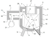
도 1은 본 발명의 실시형태에 따른 분자선 에피택시 장치를 나타낸다.1 shows a molecular beam epitaxy device according to an embodiment of the invention.
분자선 에피택시 장치는 공정 영역(2)를 둘러싸는 성장 챔버(1)을 포함한다. 성장 챔버(1)은 측벽(3), 저부 벽(4) 및 상부 벽(5)를 포함한다. 이들 벽의 각각은 내부 표면을 갖는다. 성장 챔버 벽(3,4,5)은 밀폐된 실린더의 일반적인 모양을 갖는 일체형(unitary) 어셈블리를 형성한다. The molecular beam epitaxy device comprises a growth chamber 1 surrounding the
분자선 에피택시 장치는 측벽(3)의 내부 표면을 적어도 덮는 측부(10)를 갖는 주 극저온 패널을 포함한다. 이 주 극저온 패널(10)은 예를 들어 액체 질소와 같은 극저온 유체로 냉각된다. 글리콜이 또한 극저온 유체로 사용될 수 있다. 바람직하게는, 주 극저온 패널(10)의 측 부가 원통형 모양을 갖는다. The molecular beam epitaxy device comprises a main cryogenic panel having a
분자선 에피택시 장치는 원통형 모양을 갖는 2차 극저온 패널(7)에 의해 결국 둘러싸일 수 있는 샘플 홀더(6)를 포함한다. 샘플 홀더(6)는 성장 챔버(1)의 상부에 위치하고, 기판을 지지한다. 이는 기판을 300℃ 내지 1100℃의 온도에서 가열하기 위한 가열 수단을 포함한다. The molecular beam epitaxy device comprises a
분자선 에피택시 장치는 원소들 또는 화합물의 원자 또는 분자를 증발시킬 수 있는 적어도 하나의 방출 셀(8), 및 성장 챔버(1)에 기체 전구 물질을 주입할 수 있는 기체 인젝터(9)를 포함한다. 방출 셀(8) 및 기체 인젝터(9)는 성장 챔버(1)의 바닥에 위치한다. The molecular beam epitaxy device comprises at least one
기체 전구 물질의 일부는 기판의 표면에서 원소들 또는 화합물의 원자 또는 분자와 반응하여 예를 들어 GAN과 같은 재료의 에피택시얼 층을 형성할 수 있고, 기체 전구 물질의 다른 부분은 소모되지 않는다. Some of the gaseous precursors may react with atoms or molecules of elements or compounds at the surface of the substrate to form epitaxial layers of materials such as, for example, GAN, while other portions of the gaseous precursors are not consumed.
기판은 예를 들어 실리콘, 탄화규소, 사파이어, 질화 알루미늄, 다이아몬드, 질화 갈륨 주형일 수 있다. The substrate can be, for example, silicon, silicon carbide, sapphire, aluminum nitride, diamond, gallium nitride template.
예를 들어, 증발되는 원소들 또는 화합물의 원자 또는 분자는 III 족의 금속일 수 있고, 주입되려는 원소는 V족의 원소일 수 있다. For example, the atoms or molecules of the elements or compounds to be evaporated can be Group III metals, and the elements to be implanted can be Group V elements.
바람직하게는, 분자선 에피택시 장치는 실리콘 기판의 표면에 GAN의 에피택시얼 층을 얻기 위하여 사용되고, III 족의 원소는 갈륨이며, V족의 원소를 포함하는 기체 전구 물질은 암모니아(NH3)이다. Preferably, the molecular beam epitaxy device is used to obtain an epitaxial layer of GAN on the surface of the silicon substrate, the element of group III is gallium, and the gas precursor containing element of group V is ammonia (NH 3 ). .
각 방출 셀(8)은 이동성 셔터(shutter)(나타나지 않음)를 포함하고, 예를 들어 알루미나와 같은 다양한 물질로 만들어진다. Each emitting
분자선 에피택시 장치는 성장 챔버(11)에 연결되고, 고 진공 능력을 제공할 수 있는 펌핑 수단(11)을 포함한다. The molecular beam epitaxy device is connected to the
펌핑 수단(11)은 벽(15)를 갖는 펌핑 관(duct)(30)을 포함할 수 있다. 펌핑 관(30)은 제 1 단부(12)에 의해 펌핑 장치(21)에 연결되고 제 2 단부(13)에 의해 성장 챔버(10)로 빠져나온다. The pumping means 11 may comprise a pumping
펌핑 장치(21)는 2차 펌프와 연결된 1차 펌프일 수 있다. The
주 극저온 패널(10)의 측부에는 펌핑 수단911)의 제 2 단부(13) 앞에 위치한 홀(22)이 구비된다.The side of the main
본 발명의 실시형태에 따르면, 분자선 에피택시 장치가 성장 챔버(3,4,5)의 적어도 내부 표면을 덮는 절연 밀페물(14)를 포함한다. According to an embodiment of the present invention, the molecular beam epitaxy device comprises an insulating hermetic 14 covering at least the inner surface of the
절연 밀폐물(14)은 기체 전구 물질이 원해지지 않을 때, 성장 챔버(1)안의 기체 전구 물질의 부분적인 압력을 제한하기 위하여, 기체의 흡착/탈착 변화 공정이 공정 영역(2) 주변에서 제한되거나 피해지도록 하는 온도를 갖는 냉각부와 고온부를 갖는다. The insulating
절연 밀폐물(14)은 성장 챔버 벽(3,4,5)의 내부 표면으로부터 공정 영역(2)을 절연하기 위하여, 성장 챔버 벽(3,4,5)의 내부 표면을 완전히 또는 거의 덮는다. The insulating
냉각부의 온도 Tmin은 냉각부에서 소모되지 않은 기체 전구물질을 트랩(trap)하기 위하여 기체 전구물질 용융점 이하이다. The temperature T min of the cooling section is below the gas precursor melting point to trap gas precursors not consumed in the cooling section.
냉각부의 온도 Tmin은 탈착 시간 상수가 높아 공정 영역(2)에서 암모니아의 무시할만한 유동에 이르도록 하는 정도이다.이 온도는 기체 전구물질, 예를 들어 암모니아의 용융점보다 적어도 낮아야 한다. The temperature T min of the cooling section is such that the desorption time constant is high to reach a negligible flow of ammonia in the
예를 들어, -78℃의 암모니아 용융점 아래의 온도 경우, 탈착 시간 상수가 실온에 비해 5 차수(orders) 크기로 감소한다. 따라서, 공정 영역(2)로의 오염 유동이 이 인자에 의해 수십 배 역시 감소한다. 냉각부의 온도는 암모니아를 트랩하고 이를 방출하지 않도록 충분히 낮아야 한다. For example, at temperatures below the ammonia melting point of −78 ° C., the desorption time constant decreases to 5 orders of magnitude relative to room temperature. Thus, the contaminant flow into the
유리하게는, 액체 질소의 온도(-196℃)에서, 12 차수 크기를 얻는다. Advantageously, at the temperature of liquid nitrogen (-196 ° C.), orders of
대부분의 기체 암모니아는 냉각부에 의해 트랩된다. 암모니아 경우, 절연 밀폐물(14)의 냉각 부의 펌핑 능력은 총 펌핑 능력의 약 99%이다. 질소, 탄소, 물 및 수소와 같은, 냉각 부에 의해 트랩되지 않은 잔류 종들은 펌핑 수단(11)에 의해 펌핑된다. Most of the gaseous ammonia is trapped by the cooling section. In the case of ammonia, the pumping capacity of the cooling portion of the insulating
고온 부의 온도 Tmax는 고온 부위에서 기체 전구 물질의 탈착률이 기체 전구 물질의 흡착률보다 적어도 1000배 크다. 달리 말하면, 고온 부의 온도 Tmax는 기체 전구 물질의 고정을 피하기에 충분히 높다.The temperature T max of the hot portion is at least 1000 times greater than the adsorption rate of the gas precursor at the hot site. In other words, the temperature T max of the hot portion is high enough to avoid fixation of the gaseous precursor.
고온부의 온도 Tmax는 기체 전구물질의 탈착 시간 상수가 고온부 위의 기체 전구 물질의 흡착을 제한하기 위하여 공정의 전이 기간 동안보다 미만인 온도 이상이다. The temperature T max of the hot portion is above the temperature at which the desorption time constant of the gas precursor is less than during the transition period of the process to limit the adsorption of the gas precursor on the hot portion.
전형적으로, 분(minutes) 범위의 전이 시간과 함께, 탈착 시간 상수는 초 이하이어야 한다. 분명히, 스테인리스 강 또는 탄탈룸 같은 보통의 재료상에서, 이는 +100℃ 보다 높은 온도 Tmax를 필요로 한다. Typically, with a transition time in the range of minutes, the desorption time constant should be less than or equal to seconds. Clearly, on ordinary materials such as stainless steel or tantalum, this requires a temperature T max higher than + 100 ° C.
요약하여, 기체 전구 물질로 암모니아를 사용할 때, 냉각부의 온도 Tmin은 -78℃ 이하이고, 고온부의 온도 Tmax는 +100℃ 이상이다. -78℃ 내지 +100℃ 사이의 온도를 갖는 절연 밀폐물(14)의 표면은 제한되고, 바람직하게는 제거된다. 다르게 말해서, 절연 밀폐물(14)의 온도는 Tmin 내지 Tmax 사이의 범위(암모니아 경우 -78℃ 및 +100℃)에 포함되지 않는다. In summary, when using ammonia as the gas precursor, the temperature T min of the cooling section is below -78 ° C and the temperature T max of the hot section is above + 100 ° C. The surface of the insulating
이들 온도는 예를 들어 산소와 같은 다른 전구 물질을 사용할 때 다르다. These temperatures are different when using other precursors, for example oxygen.
암모니아의 잔류 압력은 암모니아가 필요로 하지 않을 때, 즉, 성장 챔버(1)에서 기체 암모니아의 주입 전 및 후, 10-7 파스칼 미만이어야 한다. 이는 성장 공정이 교란되거나, 멈추지 않는 한계 압력이다. 바람직하게는, 암모니아의 잔류 압력은 약 10-8 파스칼이다. 비교를 위하여, 성장 공정 동안, 기체 전구 물질이 주입될 때, 암모니아의 잔류 압력은 약 10-5 파스칼이다. The residual pressure of ammonia should be less than 10 −7 Pascal when no ammonia is needed, ie before and after the injection of gaseous ammonia in the growth chamber 1. This is the threshold pressure at which the growth process does not disturb or stop. Preferably, the residual pressure of ammonia is about 10 -8 pascals. For comparison, during the growth process, when a gaseous precursor is injected, the residual pressure of ammonia is about 10-5 Pascals.
주 극저온 패널은 측 벽(3)의 내부 표면을 덮는 측부(10), 저부 벽(4)의 내부 표면을 덮는 저 부(23) 및 상부 벽(5)의 내부 표면을 덮는 상 부(26)을 포함한다. The primary cryogenic panel comprises a
절연 밀폐물(14)의 냉각부는 주 극저온 패널의 측부(10), 저 부(23), 및 상 부(26)를 포함한다. The cooling portion of the insulating
주 극저온 패널(23)의 저 부에는 방출 셀(8)용의 제 1 홀(24), 및 기체 인젝터(9)용의 제 2 홀(25)이 구비된다. The bottom of the main
주 극저온 패널(26)의 상 부에는 샘플 홀더(6)가 및 결국에는 샘플 홀더를 둘러싸는 2차 극저온 패널(7)이 가로지르는 홀(27)이 구비된다. On top of the main
다른 가능한 실시 형태에서, 절연 밀폐물(14)의 냉각부는 펌핑 수단(11)의 펌핑 관(30)의 벽(15) 내부 표면을 완전히 또는 거의 덮는 극저온 패널(16)을 포함한다. In another possible embodiment, the cooling part of the insulating
본 발명인들은 "덮는(covering)"에 의해 냉각부 상의 응축된 전구 물질이 벽에 접촉하지 않도록, 이들 내부 표면과 극저온 패널 사이에 간격 d를 두고 벽을 따라 배치된 것을 의미한다. 간격 d는 0.5 cm 내지 5 cm이다. The present inventors mean that they are disposed along the wall at a distance d between these inner surfaces and the cryogenic panel so that the condensed precursor on the cooling part is not in contact with the wall by "covering". The spacing d is between 0.5 cm and 5 cm.
바람직하게는, 주 극저온 패널의 측부(10), 주 극저온 패널의 저 부(23) 및 성장 챔버(1)의 주 극저온 패널의 상 부(26)는 극저온 유체가 순환하는 일체형 어셈블리를 형성한다.Preferably, the
이 일체형 어셈블리는 성장 챔버 벽(3,4,5)의 형태에 적합하다. This unitary assembly is suitable for the shape of the
주 극저온 패널의 부분들은 성장 챔버 벽(3,4,5)의 내부 표면의 대부분을 덮도록 설계된다. 이 극저온 패널안의 홀들은 추가로 샘플 홀더(6), 방출 셀(8), 가열 수단을 포함하는 기체 인젝터(9) 및 방출 셀의 셔터를 포함하는 고온부로 채워진다. The portions of the main cryogenic panel are designed to cover most of the inner surface of the
달리는, 주 극저온 패널(26)의 측 부(10), 저 부(23) 및 상 부는 세 개의 별개의 극저온 패널이다.Alternatively, the
도 1에 나타난 바와 같이, 유리하게는, 두드러지게 실온에서 및 보통으로는 Tmin 내지 Tmax 사이의 범위에 포함되지 않는 온도인 성장 챔버로부터 직접적인 도시는 없다. As shown in FIG. 1, there is advantageously no direct illustration from the growth chamber, which is at a temperature which is noticeably at room temperature and usually not in the range between T min and T max .
바람직한 방법으로는, 성장 챔버 벽의 80% 보다 많은 부분이 공정 영역(2)를 향하는 절연 밀폐물(14)의 고온 및 냉각 부에 의해 차폐된다. In a preferred manner, more than 80% of the growth chamber walls are shielded by the hot and cold portions of the insulating
달리는, 도 2에 나타난 바와 같이, 주 극저온 패널(10)의 측 부는 상부 단부(28)를 포함하고, 절연 밀폐물(14)의 냉각부는 주 극저온 패널(10)의 측 부의 상부 단부(28)에 연결된 제 1 열 윙(17)을 포함한다. Alternatively, as shown in FIG. 2, the side of the main
절연 밀페물(14)의 냉각 부는 2차 극저온 패널(7)의 외부 벽에 연결된 제 2 열 윙(18)을 동등하게 포함한다. The cooling section of the insulating
이들 두 개의 열 윙(17,18)은 횡으로 연장한다. 제 2 열 윙(18)은 2차 극저온 패널(7)의 외부 벽으로부터 횡으로 연장한다. 이들 두 개의 윙(17,18)은 2차 극저온 패널(7)을 둘러싸고, 성장 챔버(1)의 상부 벽(5)으로부터 공정 영역(2)을 절연하기 위하여 서로 근접해 있다. These two
간격(29)이 두 개의 열 윙(17,18) 사이에 제공된다. 바람직하게는, 열 윙(17,18)은 고리-모양이다. A
제 1 열 윙(17)은 주 극저온 패널(10)의 측 부로부터 2차 극저온 패널(7)의 부근까지 연장한다. 간격이 제 1 열 윙(17)의 단부와 2차 극저온 패널(7)의 벽 사이에 제공된다. The
제 2 열 윙(18)은 제 1 열 윙(17) 아래에 위치한다. 제 2 열 윙(18)은 제 1 열 윙(17) 보다 짧고, 제 1 열 윙(17)의 단부와 2차 극저온 패널(7) 사이에 제공된 간격 앞에 제공된다.The
열 윙(17,18)은 열 전도체로서 작용하고, 극저온 패널에 의해 냉각된다.
절연 밀폐물(14)의 고온 부는 기체 인젝터(9)에 연결된 제 3 열 윙(19)을 포함한다. 제 3 열 윙(19)은 주 극저온 패널(23)의 저 부의 제 2 홀(25)과 성장 챔버(1)의 저부 벽(4)의 내부 표면 사이에 위치한다. 제 3 열 윙(19)은 성장 챔버(1)의 저부 벽(4)의 내부 표면으로부터 공정 영역(2)을 절연시키도록 기체 인젝터(9)를 둘러싼다. The high temperature portion of the insulating
제 3 열 윙(19)은 기체 인젝터(9)의 표면으로부터 연장한다. 이는 고리-모양이다. 그의 폭은 주 극저온 패널(23)의 저 부의 제 2 홀(25)의 직경에 대략적으로 상응한다. The
증기 상태의 암모니아의 순환은 제 3 열 윙(19)과 주 극저온 패널(23)의 하 부 사이에 제한된다. The circulation of the ammonia in the vapor state is limited between the
절연 밀폐물(14)의 냉각부는 주 극저온 패널(23)의 저 부의 제 2 홀(24)에 삽입되고, 주 극저온 패널(23)의 하부로 부터 연장하는 제 4 열 윙(20)을 포함한다. 제 4 열 윙(20)은 성장 챔버(1)의 저부 벽(4)의 내부 표면으로부터 공정 영역(2)를 절연하기위하여 기체 인젝터(9)를 둘러싼다. 제 4 열 윙(20)은 고리-모양일 수 있다. The cooling section of the insulating
본 발명의 다른 가능한 실시 형태에서, 샘플 홀더(6)는 샘플 홀더(6)와 2차 극저온 패널(7)의 하부 단부(31) 사이의 열 교환을 제한하거나 피하기 위하여 2차 극저온 패널(7)의 하단(31)보다 낮다.In another possible embodiment of the invention, the
본 발명은 기체 전구 물질의 주입이 멈출 때 성장 챔버(1)에로의 기체 전구 물질의 잔류 증기압을 제한하는 것을 가능하게 한다. 따라서, 성장 공정은 교란되지 않는다.
The present invention makes it possible to limit the residual vapor pressure of the gas precursor into the growth chamber 1 when the injection of the gas precursor is stopped. Thus, the growth process is not disturbed.
(1) : 성장 챔버
(2) : 공정 영역
(3) : 측 벽
(4) : 저부 벽
(5) : 상부 벽
(6) : 샘플 홀더
(7) : 2차 극저온 패널
(8) : 방출 셀
(9) : 기체 인젝터
(10) : 주 극저온 패널의 측부
(11) : 펌핑 웰
(12) : 제 1 단부
(13) : 제 2 단부
(14) : 절연 밀폐물
(15) : 벽
(16) : 극저온 패널
(17) : 제 1 열 윙
(18) : 제 2 열 윙
(19) : 제 3 열 윙
(20) : 제 4 열 윙
(21) : 펌핑 장치
(22) : 홀
(23) : 주 극저온 패널의 저 부
(24) : 제 1 홀
(25) : 제 2 홀
(26) : 주 극저온 패널의 상 부
(27) : 홀
(28) : 상부 단부
(29) : 간격
(30) : 펌핑 관
(31) : 하부 단부(1): growth chamber
(2): process area
(3): side wall
(4): bottom wall
(5): upper wall
(6): sample holder
(7): 2nd cryogenic panel
(8): emitting cell
(9): gas injector
(10): side of the main cryogenic panel
(11): pumping well
12: first end
(13): second end
14: insulation seal
15: wall
16: cryogenic panel
17: first row wing
18: second row wing
19: third row wing
20: fourth row wing
21: pumping device
22: hall
(23): bottom of main cryogenic panel
24: the first hole
25: the second hall
(26): Upper part of the main cryogenic panel
(27): hall
28: upper end
(29): spacing
30: pumping pipe
31: lower end
Claims (13)
- 각각 내부 표면을 갖는 측벽(3), 하부 벽(4) 및 상부 벽(5)을 포함하는, 공정 영역(2)을 둘러싸는 성장 챔버(1),
- 상기 측벽(3)의 내부 표면을 덮는 적어도 하나의 측 부(lateral part)(10)를 갖는 주 극저온 패널,
- 가열 수단을 포함하는, 상기 기판을 지지할 수 있는 샘플 홀더(6),
- 원소들 또는 화합물의 원자 또는 분자를 증발시킬 수 있는 적어도 하나의 방출 셀(8),
- 성장 챔버(1)에 기체 전구 물질을 주입시킬 수 있는 기체 인젝터(injector)(9)로서, 상기 기체 전구 물질의 일 부분은 기판의 표면 위의 원소들 또는 화합물의 원자 또는 분자와 반응할 수 있어 상기 층을 형성하는 기체 인젝터(9),
- 성장 챔버(1)에 연결되고, 고 진공 능력을 제공할 수 있는 펌핑 수단(11)을 추가로 포함하고,
상기 성장 챔버 벽(3,4,5)의 적어도 내부 표면을 덮는 절연 밀폐물(14)을 포함하고, 상기 절연 밀폐물(14)은 기체 전구 물질의 융점 이하의 온도 Tmin을 갖는 냉각 부(cold parts), 고온 부(hot parts)상의 기체 전구 물질의 탈착률이 상기 기체 전구 물질의 흡착률보다 적어도 1000 배 큰 온도 이상의 온도 Tmax를 갖는 고온 부를 포함함을 특징으로 하는 반도체 재료의 웨이퍼를 제조하기 위한 분자선 에피택시 장치.A molecular beam epitaxy apparatus for manufacturing a wafer of semiconductor material comprising a substrate covered by a material layer,
A growth chamber 1 surrounding the process region 2, each comprising a side wall 3 with an inner surface, a lower wall 4 and an upper wall 5,
A primary cryogenic panel having at least one lateral part 10 covering the inner surface of the side wall 3,
A sample holder 6 capable of supporting the substrate, comprising heating means,
At least one emitting cell 8 capable of evaporating atoms or molecules of elements or compounds,
A gas injector 9 capable of injecting a gas precursor into the growth chamber 1, wherein a portion of the gas precursor is capable of reacting with atoms or molecules of elements or compounds on the surface of the substrate There is a gas injector 9 forming the layer,
Further comprising pumping means 11 connected to the growth chamber 1 and capable of providing high vacuum capability,
An insulating seal 14 covering at least an inner surface of the growth chamber walls 3, 4, 5, wherein the insulating seal 14 has a cooling portion having a temperature T min below the melting point of the gaseous precursor material. cold parts, a hot part having a temperature T max at which the desorption rate of the gas precursor on the hot parts is at least 1000 times greater than the adsorption rate of the gas precursor. Molecular beam epitaxy device for manufacturing.
- 측벽(3)의 내부 표면을 덮고, 펌핑 수단(11)과 연결을 위한 홀(hole)(22)이 구비된 주 극저온 패널(10)의 상기 측벽 부,
- 저부 벽(4)의 내부 표면을 덮고, 방출 셀(8)용 제 1 홀(24), 및 기체 인젝터(9)용 제 2 홀(25)이 구비된 주 극저온 패널(23)의 저 부(lower part),
- 상부 벽(5)의 내부 표면을 덮고, 상기 샘플 홀더(6)에 의해 가로질러진 홀(27)이 구비된 주 극저온 패널(26)의 상 부(upper part)를 포함하는 것을 특징으로 하는 분자선 에피택시 장치.The cooling part according to any one of claims 1 to 4, wherein the cooling portion of the insulating seal (14) is
The side wall part of the main cryogenic panel 10, which covers the inner surface of the side wall 3 and is provided with holes 22 for connection with the pumping means 11,
The bottom of the main cryogenic panel 23 which covers the inner surface of the bottom wall 4 and is equipped with a first hole 24 for the discharge cell 8 and a second hole 25 for the gas injector 9. (lower part),
An upper part of the main cryogenic panel 26, which covers the inner surface of the upper wall 5 and is provided with a hole 27 intersected by the sample holder 6. Molecular beam epitaxy device.
13. The sample holder according to claim 9, wherein the sample holder 6 is adapted to limit or avoid thermal changes between the sample holder 6 and the lower end of the secondary cryogenic panel 7. A molecular beam epitaxy device, characterized in that it is lower than the lower end of the secondary cryogenic panel (7).
Applications Claiming Priority (2)
| Application Number | Priority Date | Filing Date | Title |
|---|---|---|---|
| EP09305570.5 | 2009-06-18 | ||
| EP09305570A EP2264225B1 (en) | 2009-06-18 | 2009-06-18 | Molecular beam epitaxy apparatus for producing wafers of semiconductor material |
Publications (1)
| Publication Number | Publication Date |
|---|---|
| KR20120040152A true KR20120040152A (en) | 2012-04-26 |
Family
ID=41327683
Family Applications (1)
| Application Number | Title | Priority Date | Filing Date |
|---|---|---|---|
| KR1020117030375A KR20120040152A (en) | 2009-06-18 | 2010-06-17 | Molecular beam epitaxy apparatus for producing wafers of semiconductor material |
Country Status (9)
| Country | Link |
|---|---|
| US (1) | US20120097105A1 (en) |
| EP (1) | EP2264225B1 (en) |
| JP (1) | JP2012530371A (en) |
| KR (1) | KR20120040152A (en) |
| CN (1) | CN102803580A (en) |
| ES (1) | ES2391246T3 (en) |
| PL (1) | PL2264225T3 (en) |
| SG (1) | SG176907A1 (en) |
| WO (1) | WO2010146129A1 (en) |
Families Citing this family (1)
| Publication number | Priority date | Publication date | Assignee | Title |
|---|---|---|---|---|
| US11519095B2 (en) | 2019-04-22 | 2022-12-06 | Peng DU | MBE system with direct evaporation pump to cold panel |
Family Cites Families (13)
| Publication number | Priority date | Publication date | Assignee | Title |
|---|---|---|---|---|
| US571181A (en) | 1896-11-10 | Field-magnet pole | ||
| FR1587077A (en) * | 1968-08-01 | 1970-03-13 | ||
| US4330360A (en) * | 1980-07-21 | 1982-05-18 | Bell Telephone Laboratories, Incorporated | Molecular beam deposition technique using gaseous sources of group V elements |
| JPS6261315A (en) * | 1985-09-11 | 1987-03-18 | Sharp Corp | Molecular beam epitaxy device |
| GB2204066A (en) * | 1987-04-06 | 1988-11-02 | Philips Electronic Associated | A method for manufacturing a semiconductor device having a layered structure |
| JPH069297A (en) * | 1991-12-09 | 1994-01-18 | Sumitomo Electric Ind Ltd | Film forming device |
| JPH0897147A (en) * | 1994-09-29 | 1996-04-12 | Mitsubishi Electric Corp | Epitaxial crystal growth device |
| US5788776A (en) * | 1996-12-02 | 1998-08-04 | Chorus Corporation | Molecular beam epitaxy isolation tube system |
| FR2840925B1 (en) * | 2002-06-18 | 2005-04-01 | Riber | VAPOR MATERIAL EVAPORATION CHAMBER WITH DIFFERENTIAL PUMPING |
| US6718775B2 (en) * | 2002-07-30 | 2004-04-13 | Applied Epi, Inc. | Dual chamber cooling system with cryogenic and non-cryogenic chambers for ultra high vacuum system |
| US7446474B2 (en) * | 2002-10-10 | 2008-11-04 | Applied Materials, Inc. | Hetero-junction electron emitter with Group III nitride and activated alkali halide |
| EP2066415A2 (en) | 2006-09-25 | 2009-06-10 | Veeco Instruments Inc. | Thermally isolated cryopanel for vacuum deposition sytems |
| DE102007054851A1 (en) * | 2007-11-16 | 2009-05-20 | Createc Fischer & Co. Gmbh | MBE facility and method of operation |
-
2009
- 2009-06-18 EP EP09305570A patent/EP2264225B1/en active Active
- 2009-06-18 ES ES09305570T patent/ES2391246T3/en active Active
- 2009-06-18 PL PL09305570T patent/PL2264225T3/en unknown
-
2010
- 2010-06-17 SG SG2011093820A patent/SG176907A1/en unknown
- 2010-06-17 WO PCT/EP2010/058569 patent/WO2010146129A1/en active Application Filing
- 2010-06-17 US US13/379,175 patent/US20120097105A1/en not_active Abandoned
- 2010-06-17 CN CN2010800361457A patent/CN102803580A/en active Pending
- 2010-06-17 JP JP2012515501A patent/JP2012530371A/en active Pending
- 2010-06-17 KR KR1020117030375A patent/KR20120040152A/en not_active Application Discontinuation
Also Published As
| Publication number | Publication date |
|---|---|
| EP2264225B1 (en) | 2012-08-29 |
| JP2012530371A (en) | 2012-11-29 |
| CN102803580A (en) | 2012-11-28 |
| SG176907A1 (en) | 2012-01-30 |
| US20120097105A1 (en) | 2012-04-26 |
| EP2264225A1 (en) | 2010-12-22 |
| PL2264225T3 (en) | 2013-01-31 |
| ES2391246T3 (en) | 2012-11-22 |
| WO2010146129A1 (en) | 2010-12-23 |
Similar Documents
| Publication | Publication Date | Title |
|---|---|---|
| JP5645718B2 (en) | Heat treatment equipment | |
| US20130260537A1 (en) | System and process for high-density, low-energy plasma enhanced vapor phase epitaxy | |
| US20190317125A1 (en) | Microscopy sample stage for gas hydrate tests and temperature and pressure controlling system of the stage | |
| EP2107138B1 (en) | Apparatus for producing silicon carbide single crystal | |
| KR20110066856A (en) | Substrate processing apparatus and method of manufacturing semiconductor device | |
| US6718775B2 (en) | Dual chamber cooling system with cryogenic and non-cryogenic chambers for ultra high vacuum system | |
| KR20120040152A (en) | Molecular beam epitaxy apparatus for producing wafers of semiconductor material | |
| US8858713B2 (en) | Apparatus for depositing a thin film of material on a substrate and regeneration process for such an apparatus | |
| KR100998012B1 (en) | Apparatus for Chemical Vapor Deposition | |
| KR20140018148A (en) | Method and apparatus of forming compound semiconductor film | |
| KR101210064B1 (en) | Vacuum heat treatment apparatus | |
| EP1330561B1 (en) | Integrated phase separator for ultra high vacuum system | |
| KR101469502B1 (en) | High temperature chemical vapor deposition apparatus for growing single crystal | |
| JP7383096B2 (en) | Substrate processing equipment | |
| JP2009249201A (en) | Apparatus for producing aluminum nitride single crystal | |
| KR101210157B1 (en) | Vacuum heat treatment apparatus | |
| CN115896945A (en) | Silicon carbide powder synthesizing device and method | |
| JP2004288964A (en) | PROCESS FOR GROWING GaN CRYSTAL | |
| JP3214133B2 (en) | Epitaxial growth apparatus and epitaxial growth method | |
| KR20120140147A (en) | Deposition apparatus | |
| KR20160077589A (en) | Apparatus for growing semi-insulating silicon carbide single crystal | |
| KR20130048440A (en) | Apparatus and method for deposition |
Legal Events
| Date | Code | Title | Description |
|---|---|---|---|
| WITN | Application deemed withdrawn, e.g. because no request for examination was filed or no examination fee was paid |