KR20120026991A - Photoresist compositions and methods of forming photolithographic patterns - Google Patents
Photoresist compositions and methods of forming photolithographic patterns Download PDFInfo
- Publication number
- KR20120026991A KR20120026991A KR1020110091582A KR20110091582A KR20120026991A KR 20120026991 A KR20120026991 A KR 20120026991A KR 1020110091582 A KR1020110091582 A KR 1020110091582A KR 20110091582 A KR20110091582 A KR 20110091582A KR 20120026991 A KR20120026991 A KR 20120026991A
- Authority
- KR
- South Korea
- Prior art keywords
- photoresist composition
- photoresist
- layer
- cyclic
- monomer
- Prior art date
Links
Images


Classifications
-
- G—PHYSICS
- G03—PHOTOGRAPHY; CINEMATOGRAPHY; ANALOGOUS TECHNIQUES USING WAVES OTHER THAN OPTICAL WAVES; ELECTROGRAPHY; HOLOGRAPHY
- G03F—PHOTOMECHANICAL PRODUCTION OF TEXTURED OR PATTERNED SURFACES, e.g. FOR PRINTING, FOR PROCESSING OF SEMICONDUCTOR DEVICES; MATERIALS THEREFOR; ORIGINALS THEREFOR; APPARATUS SPECIALLY ADAPTED THEREFOR
- G03F7/00—Photomechanical, e.g. photolithographic, production of textured or patterned surfaces, e.g. printing surfaces; Materials therefor, e.g. comprising photoresists; Apparatus specially adapted therefor
- G03F7/004—Photosensitive materials
- G03F7/039—Macromolecular compounds which are photodegradable, e.g. positive electron resists
- G03F7/0392—Macromolecular compounds which are photodegradable, e.g. positive electron resists the macromolecular compound being present in a chemically amplified positive photoresist composition
- G03F7/0397—Macromolecular compounds which are photodegradable, e.g. positive electron resists the macromolecular compound being present in a chemically amplified positive photoresist composition the macromolecular compound having an alicyclic moiety in a side chain
-
- G—PHYSICS
- G03—PHOTOGRAPHY; CINEMATOGRAPHY; ANALOGOUS TECHNIQUES USING WAVES OTHER THAN OPTICAL WAVES; ELECTROGRAPHY; HOLOGRAPHY
- G03F—PHOTOMECHANICAL PRODUCTION OF TEXTURED OR PATTERNED SURFACES, e.g. FOR PRINTING, FOR PROCESSING OF SEMICONDUCTOR DEVICES; MATERIALS THEREFOR; ORIGINALS THEREFOR; APPARATUS SPECIALLY ADAPTED THEREFOR
- G03F7/00—Photomechanical, e.g. photolithographic, production of textured or patterned surfaces, e.g. printing surfaces; Materials therefor, e.g. comprising photoresists; Apparatus specially adapted therefor
- G03F7/004—Photosensitive materials
- G03F7/0045—Photosensitive materials with organic non-macromolecular light-sensitive compounds not otherwise provided for, e.g. dissolution inhibitors
-
- G—PHYSICS
- G03—PHOTOGRAPHY; CINEMATOGRAPHY; ANALOGOUS TECHNIQUES USING WAVES OTHER THAN OPTICAL WAVES; ELECTROGRAPHY; HOLOGRAPHY
- G03F—PHOTOMECHANICAL PRODUCTION OF TEXTURED OR PATTERNED SURFACES, e.g. FOR PRINTING, FOR PROCESSING OF SEMICONDUCTOR DEVICES; MATERIALS THEREFOR; ORIGINALS THEREFOR; APPARATUS SPECIALLY ADAPTED THEREFOR
- G03F7/00—Photomechanical, e.g. photolithographic, production of textured or patterned surfaces, e.g. printing surfaces; Materials therefor, e.g. comprising photoresists; Apparatus specially adapted therefor
- G03F7/004—Photosensitive materials
- G03F7/0047—Photosensitive materials characterised by additives for obtaining a metallic or ceramic pattern, e.g. by firing
-
- G—PHYSICS
- G03—PHOTOGRAPHY; CINEMATOGRAPHY; ANALOGOUS TECHNIQUES USING WAVES OTHER THAN OPTICAL WAVES; ELECTROGRAPHY; HOLOGRAPHY
- G03F—PHOTOMECHANICAL PRODUCTION OF TEXTURED OR PATTERNED SURFACES, e.g. FOR PRINTING, FOR PROCESSING OF SEMICONDUCTOR DEVICES; MATERIALS THEREFOR; ORIGINALS THEREFOR; APPARATUS SPECIALLY ADAPTED THEREFOR
- G03F7/00—Photomechanical, e.g. photolithographic, production of textured or patterned surfaces, e.g. printing surfaces; Materials therefor, e.g. comprising photoresists; Apparatus specially adapted therefor
- G03F7/004—Photosensitive materials
- G03F7/027—Non-macromolecular photopolymerisable compounds having carbon-to-carbon double bonds, e.g. ethylenic compounds
-
- G—PHYSICS
- G03—PHOTOGRAPHY; CINEMATOGRAPHY; ANALOGOUS TECHNIQUES USING WAVES OTHER THAN OPTICAL WAVES; ELECTROGRAPHY; HOLOGRAPHY
- G03F—PHOTOMECHANICAL PRODUCTION OF TEXTURED OR PATTERNED SURFACES, e.g. FOR PRINTING, FOR PROCESSING OF SEMICONDUCTOR DEVICES; MATERIALS THEREFOR; ORIGINALS THEREFOR; APPARATUS SPECIALLY ADAPTED THEREFOR
- G03F7/00—Photomechanical, e.g. photolithographic, production of textured or patterned surfaces, e.g. printing surfaces; Materials therefor, e.g. comprising photoresists; Apparatus specially adapted therefor
- G03F7/004—Photosensitive materials
- G03F7/039—Macromolecular compounds which are photodegradable, e.g. positive electron resists
- G03F7/0392—Macromolecular compounds which are photodegradable, e.g. positive electron resists the macromolecular compound being present in a chemically amplified positive photoresist composition
-
- G—PHYSICS
- G03—PHOTOGRAPHY; CINEMATOGRAPHY; ANALOGOUS TECHNIQUES USING WAVES OTHER THAN OPTICAL WAVES; ELECTROGRAPHY; HOLOGRAPHY
- G03F—PHOTOMECHANICAL PRODUCTION OF TEXTURED OR PATTERNED SURFACES, e.g. FOR PRINTING, FOR PROCESSING OF SEMICONDUCTOR DEVICES; MATERIALS THEREFOR; ORIGINALS THEREFOR; APPARATUS SPECIALLY ADAPTED THEREFOR
- G03F7/00—Photomechanical, e.g. photolithographic, production of textured or patterned surfaces, e.g. printing surfaces; Materials therefor, e.g. comprising photoresists; Apparatus specially adapted therefor
- G03F7/20—Exposure; Apparatus therefor
- G03F7/2041—Exposure; Apparatus therefor in the presence of a fluid, e.g. immersion; using fluid cooling means
-
- G—PHYSICS
- G03—PHOTOGRAPHY; CINEMATOGRAPHY; ANALOGOUS TECHNIQUES USING WAVES OTHER THAN OPTICAL WAVES; ELECTROGRAPHY; HOLOGRAPHY
- G03F—PHOTOMECHANICAL PRODUCTION OF TEXTURED OR PATTERNED SURFACES, e.g. FOR PRINTING, FOR PROCESSING OF SEMICONDUCTOR DEVICES; MATERIALS THEREFOR; ORIGINALS THEREFOR; APPARATUS SPECIALLY ADAPTED THEREFOR
- G03F7/00—Photomechanical, e.g. photolithographic, production of textured or patterned surfaces, e.g. printing surfaces; Materials therefor, e.g. comprising photoresists; Apparatus specially adapted therefor
- G03F7/26—Processing photosensitive materials; Apparatus therefor
- G03F7/30—Imagewise removal using liquid means
- G03F7/32—Liquid compositions therefor, e.g. developers
- G03F7/325—Non-aqueous compositions
Abstract
Description
본 발명은 일반적으로 전자 디바이스의 제조에 관한 것이다. 보다 상세하게, 본 발명은 포토레지스트 조성물 및 네가티브 톤 현상 공정을 사용하여 미세 패턴을 형성할 수 있는 포토리소그래피 공정에 관한 것이다. 포토레지스트 조성물은 특정 아세탈 부분을 포함하는 모노머로부터 부분적으로 형성된 코폴리머를 포함한다. 본 발명의 바람직한 조성물 및 방법은 포토리소그래피 처리시 두께 손실을 감소시키고, 패턴 붕괴 마진(collapse margin)을 개선시킬 수 있다.The present invention relates generally to the manufacture of electronic devices. More particularly, the present invention relates to photolithography processes capable of forming fine patterns using photoresist compositions and negative tone development processes. The photoresist composition comprises a copolymer partially formed from monomers comprising specific acetal moieties. Preferred compositions and methods of the present invention can reduce thickness loss during photolithographic processing and improve pattern collapse margins.
반도체 제조 산업에 있어서, 포토레지스트 물질은 이미지를 하나 이상의 하부(underlying) 층, 예컨대 기판 자체뿐만 아니라, 반도체 기판 위에 배치된 금속, 반도체 및 유전체 층에 전달하는데 사용된다. 반도체 장치의 집적 밀도를 증가시키고 나노미터(nm) 범위의 크기를 갖는 구조물의 형성을 가능케 하기 위하여, 고-해상능을 가진 포토레지스트 및 포토리소그래피 처리 도구(tool)가 개발되었고 계속 개발 중에 있다.In the semiconductor manufacturing industry, photoresist materials are used to transfer images to one or more underlying layers, such as the substrate itself, as well as metal, semiconductor, and dielectric layers disposed over the semiconductor substrate. In order to increase the integration density of semiconductor devices and to enable the formation of structures with sizes in the nanometer (nm) range, high-resolution photoresist and photolithography processing tools have been developed and are under development.
반도체 장치에서 나노미터-스케일 피처 크기를 달성하기 위한 한 방법은 화학적으로 증폭된 포토레지스트의 노광중에 단파장, 예를 들어 193 nm 이하의 광을 사용하는 것이다. 침지(immersion) 리소그래피는, 예를 들어 KrF 또는 ArF 광원을 갖는 스캐너와 같은 이미지화 장치의 렌즈 개구수(numerical aperture)를 효과적으로 증가시킨다. 이는 이미지화 장치의 최종 표면과 반도체 웨이퍼의 상부 표면 사이에 상대적으로 고 굴절율 유체(즉, 침지 유체)를 사용함으로써 달성된다. 침지 유체는 공기 또는 비활성 가스 매질을 사용한 것보다 훨씬 많은 양의 광을 레지스트 층에 집중되도록 할 수 있다.One way to achieve nanometer-scale feature sizes in semiconductor devices is to use short wavelengths, for example 193 nm or less, during exposure of chemically amplified photoresists. Immersion lithography effectively increases the lens numerical aperture of an imaging device, for example a scanner with a KrF or ArF light source. This is accomplished by using a relatively high refractive index fluid (ie, immersion fluid) between the final surface of the imaging device and the upper surface of the semiconductor wafer. Immersion fluids can cause much more light to be concentrated in the resist layer than with air or an inert gas medium.
레일리 방정식(Rayleigh equation)에 의해 정의되는 이론적 해상 한계(resolution limit)는 다음과 같다:The theoretical resolution limits defined by the Rayleigh equation are as follows:
![]()
![]()
상기 식에서,Where
k 1은 처리 인자(process factor)이고, k 1 is the process factor,
λ는 이미지화 툴의 파장이며,λ is the wavelength of the imaging tool,
NA는 이미지화 렌즈의 개구수이다. NA is the numerical aperture of the imaging lens.
침지 유체로 물을 사용할 경우, 최대 개구수는, 예를 들어 1.2에서 1.35로 증가할 수 있다. 라인 및 스페이스 패턴을 프린팅하는 경우 k 1이 0.25일 때, 193 nm 침지 스캐너는 36 nm 절반(half)-피치 라인 및 스페이스 패턴만을 분할할 수 있을 것이다. 접촉 홀 또는 임의의 2D 패턴을 프린팅하기 위한 해상도는, k 1에 대한 이론적 한계가 0.35인 다크 필드 마스크(dark field mask)를 갖는 낮은 공간 이미지 콘트라스트(contrast)로 인해 보다 제한적이다. 따라서, 접촉 홀의 가장 작은 절반-피치는 약 50 nm로 제한된다. 표준 침지 리소그래피 공정은 일반적으로 보다 높은 해상도를 요구하는 디바이스의 제조에는 적합하지 않다.When water is used as the immersion fluid, the maximum numerical aperture can increase, for example, from 1.2 to 1.35. When printing line and space patterns When k 1 is 0.25, the 193 nm immersion scanner will be able to split only 36 nm half-pitch line and space patterns. The resolution for printing contact holes or any 2D pattern is more limited due to the low spatial image contrast with dark field mask with a theoretical limit of k 1 of 0.35. Thus, the smallest half-pitch of the contact holes is limited to about 50 nm. Standard immersion lithography processes are generally not suitable for the manufacture of devices that require higher resolution.
침지 리소그래피에서 포지티브 톤 현상의 실제 해상능을 확장하기 위해 물질 및 처리 관점 모두에서 상당한 노력이 있어 왔다. 이러한 일 예는 전통적 포지티브형 화학적 증폭 포토레지스트의 네가티브 톤 현상(negative tone development, NTD)을 포함한다. NTD는 임계 다크 필드 층의 프린팅을 위해 브라이트 필드 마스크(bright field mask)로 얻어지는 월등한 이미지화 품질을 사용할 수 있게 하는 이미지 반전 기술이다. NTD 레지스트는 전형적으로 산-불안정성(acid-labile) (또는 산-절단성(acid-cleavable)) 기 및 포토애시드 발생제(photoacid generator)를 갖는 수지를 이용한다. 화학 조사선(actinic radiation)에 노광시키면 포토애시드 발생제가 산을 형성하게 되고, 이 산이 노광후 베이킹(post-exposure baking) 동안 수지 내의 산-불안정성 기를 절단시킨다. 결과적으로, 레지스트의 노광 영역과 비노광 영역 간에 특별한 유기 현상제에서의 용해도 특성 차이가 생기며 레지스트의 비노광 영역은 현상제에 의해 제거되어 불용성의 노광 영역에 의해 생성되는 패턴이 남게 된다. 이러한 공정은, 예를 들어, 구달(Goodall) 등의 미국 특허 제6,790,579호에 기재되어 있다. 이 문헌은 산-발생 개시제 및 폴리머 백본을 따라 반복되는(recurring) 산-불안정성 펜던트(pendant) 기를 함유하는 폴리사이클릭 폴리머를 포함하는 포토레지스트 조성물을 개시한다. 노광 영역을 알칼리 현상제로 선택적으로 제거하거나, 비노광 영역을 네가티브 톤 현상을 위한 적절한 비극성 용매로 처리하여 선택적으로 제거할 수 있다.Considerable efforts have been made both from a material and processing standpoint to extend the actual resolution of positive tone phenomena in immersion lithography. One such example includes the negative tone development (NTD) of traditional positive chemically amplified photoresists. NTD is an image reversal technique that allows the use of superior imaging qualities obtained with bright field masks for printing critical dark field layers. NTD resists typically use resins having acid-labile (or acid-cleavable) groups and photoacid generators. Exposure to actinic radiation causes the photoacid generator to form acid, which cleaves acid-labile groups in the resin during post-exposure baking. As a result, there is a difference in solubility characteristics in a particular organic developer between the exposed and non-exposed areas of the resist, and the unexposed areas of the resist are removed by the developer, leaving a pattern produced by the insoluble exposed area. Such a process is described, for example, in US Pat. No. 6,790,579 to Goodall et al. This document discloses photoresist compositions comprising an acid-generating initiator and a polycyclic polymer containing acid-labile pendant groups that are recurring along the polymer backbone. The exposed areas can be selectively removed with an alkaline developer or the non-exposed areas can be selectively removed by treatment with a suitable nonpolar solvent for negative tone development.
통상의 193 nm 포토레지스트는 네가티브 톤 현상으로부터 공중 이미지 질 개선이라는 이점을 얻을 수 있지만, 표준 포지티브 톤 현상 기술에 비해 하나 이상의 단점을 나타내는 경향이 있다. 현상된 포토레지스트는 예를 들어, 노광전 레지스트 층보다 상당한 두께 손실을 입을 수 있다. 이같은 두께 손실은 통상 사용되는 산 불안정성 기, 예컨대 삼급 알킬 에스테르 기가 레지스트 층으로부터 절단되는 것에 기인하는 것으로 판단된다. 이는 하부층의 에칭동안 레지스트 패턴 영역이 완전 부식되는 경우 특히 문제가 된다. 필름이 두꺼워지면 패턴 붕괴 및 초점 깊이 감소와 같은 다른 문제가 발생할 수 있기 때문에, 이러한 문제는 더 두꺼운 레지스트 층을 사용하여서 피할 수는 없다. 전형적인 193 nm 레지스트에서 패턴 붕괴 발생은 (메트)아크릴레이트-기반 폴리머로부터 특정 산-불안정성 기, 예를 들어, 삼급 알킬 에스테르 및 아세탈 이탈기의 절단 후 포토레지스트의 노광 영역에서 발생되는 비교적 다량의 (메트)아크릴산 단위에 의해 악화되는 것으로 여겨진다. (메트)아크릴산 단위는 레지스트 패턴과 기판 사이의 극석 미스매치에 따른 유기 및 Si-기반 무기 기판에 좋지 않은 접착성에 기여한다. 통상의 193 nm 포토레지스트를 사용하여 일어날 수 있는 또 다른 문제는 내에칭성 손실이다. 이 문제는 또한 전형적으로 포지티브 톤 현상 공정에 있어 포토레지스트 패턴에 내에칭성을 부여하는 산-불안정성 삼급 알킬 기의 손실로 일어날 수 있다.Conventional 193 nm photoresists can benefit from improved aerial image quality from negative tone development, but tend to exhibit one or more disadvantages over standard positive tone development techniques. The developed photoresist may, for example, suffer significant thickness loss than the pre-exposure resist layer. This thickness loss is believed to be due to the cleavage of the acid labile groups commonly used, such as tertiary alkyl ester groups, from the resist layer. This is especially a problem when the resist pattern region is completely corroded during etching of the underlying layer. This problem cannot be avoided by using a thicker layer of resist, because thicker films can cause other problems such as pattern collapse and reduced depth of focus. The pattern collapse occurrence in a typical 193 nm resist is a relatively large amount of (in the exposed area of the photoresist after cleavage of certain acid-labile groups such as tertiary alkyl esters and acetal leaving groups from the (meth) acrylate-based polymer) It is believed to be exacerbated by meth) acrylic acid units. (Meth) acrylic acid units contribute to poor adhesion to organic and Si-based inorganic substrates due to polar mismatches between resist patterns and substrates. Another problem that can occur with conventional 193 nm photoresists is the loss of etch resistance. This problem may also arise with the loss of acid-labile tertiary alkyl groups, which typically impart etch resistance to the photoresist pattern in positive tone development processes.
전자 디바이스 제조에서 미세 패턴을 형성할 수 있고 당업계가 직면하고 있는 하나 이상의 문제점을 다룬 개선된 네가티브 톤 현상용 조성물 및 포토리소그래피 방법이 당업계에서 지속적으로 요구된다.There is a continuing need in the art for improved negative tone development compositions and photolithography methods capable of forming fine patterns in electronic device manufacturing and addressing one or more problems facing the art.
본 발명의 제1 측면에 따라, 포토레지스트 조성물이 제공된다. 이 포토레지스트 조성물은 중합성 작용기 및 하기 화학식 (I) 또는 화학식 (II)의 제1 부분을 포함하는 모노머로부터 형성된 제1 단위 및 하나 이상의 추가 단위를 포함하며 절단으로 카복실산 기를 형성할 수 있는 산 절단기를 함유하지 않는 코폴리머; 및 포토애시드 발생제(photoacid generator)를 포함한다:According to a first aspect of the invention, a photoresist composition is provided. This photoresist composition comprises an acid cutter capable of forming a carboxylic acid group by cleavage comprising a first unit formed from a monomer comprising a polymerizable functional group and a first portion of formula (I) or formula (II) and at least one additional unit Copolymers containing no; And photoacid generators:


상기 식에서,Where
R1 및 R2는 독립적으로 (C1-C10) 선형, 분지형 및 환형 유기 기로부터 선택되거나, 또는 함께, 임의로 환을 형성하며;R 1 and R 2 is independently selected from (C 1 -C 10 ) linear, branched and cyclic organic groups, or together, optionally forms a ring;
a 또는 b중 하나는 1이고, a 또는 b중 다른 하나는 1 또는 2이며;one of a or b is 1 and the other of a or b is 1 or 2;
R3 및 R4는 독립적으로 (C1-C10) 선형, 분지형 및 환형 유기 기로부터 선택되거나, 또는 함께, 임의로 환을 형성하며;R 3 and R 4 is independently selected from (C 1 -C 10 ) linear, branched and cyclic organic groups, or together, optionally forms a ring;
c 또는 d중 하나는 1이고, c 또는 d중 다른 하나는 1 또는 2이다.one of c or d is 1 and the other of c or d is 1 or 2.
또 다른 측면에 따라, 포토리소그래피 패턴의 형성 방법이 제공된다. 본 방법은 (a) 기판 표면상에 패턴화될 하나 이상의 층을 포함하는 기판을 제공하는 단계; (b) 상기 패턴화될 하나 이상의 층 위에 본 발명의 포토레지스트 조성물의 층을 도포하는 단계; (c) 상기 포토레지스트 조성물 층을 화학 조사선에 패턴식(patternwise)으로 노광시키는 단계; (d) 상기 노광된 포토레지스트 조성물 층을 노광후 베이킹(post-exposure bake) 공정에서 가열하는 단계; 및 (e) 상기 포토레지스트 조성물 층에 현상제를 적용하는 단계를 포함한다. 포토레지스트 층의 비노광 영역은 현상제에 의해 제거되고, 포토레지스트 패턴의 노광 영역은 패턴화될 하나 이상의 층 위에 포토레지스트 패턴을 형성한다.According to another aspect, a method of forming a photolithography pattern is provided. The method includes (a) providing a substrate comprising one or more layers to be patterned on the substrate surface; (b) applying a layer of the photoresist composition of the present invention over the one or more layers to be patterned; (c) patternwise exposing the photoresist composition layer to actinic radiation; (d) heating the exposed photoresist composition layer in a post-exposure bake process; And (e) applying a developer to the photoresist composition layer. The unexposed areas of the photoresist layer are removed by a developer, and the exposed areas of the photoresist pattern form a photoresist pattern over one or more layers to be patterned.
코팅 기판이 또한 제공된다. 코팅 기판은 기판과 기판 표면상에 본 원에 기재된 본 발명의 포토레지스트 조성물층을 포함한다.Coated substrates are also provided. The coated substrate comprises a substrate and a photoresist composition layer of the invention described herein on the substrate surface.
본 원에 기재된 본 발명의 네가티브 톤 현상 방법에 의해 형성된 전자 디바이스도 또한 제공된다. Also provided is an electronic device formed by the negative tone developing method of the present invention described herein.
본 원에서, "g"는 그램을 의미하고; wt%는 중량 퍼센트를 의미하며; "L"은 리터를 의미하고; "mL"은 밀리리터를 의미하며; "nm"은 나노미터를 의미하고; "mm"은 밀리미터를 의미하며; "min"은 분을 의미하고; "h"는 시간을 의미하며; "Å"은 옹스트롬을 의미하고; "mol%"는 몰 퍼센트를 의미하며; "Mw"는 중량평균분자량을 의미하고; "Mn"은 수평균분자량을 의미하며; 단수는 복수의 개념도 포함하고; 용어 "코폴리머"는 2 이상의 상이한 구조의 모노머로부터 유도된 폴리머를 의미한다.As used herein, "g" means grams; wt% means weight percent; "L" means liter; "mL" means milliliters; "nm" means nanometers; "mm" means millimeters; "min" means minutes; "h" means time; "Å" means angstroms; "mol%" means mole percent; "Mw" means weight average molecular weight; "Mn" means number average molecular weight; The singular also includes the plural concept; The term "copolymer" means a polymer derived from monomers of two or more different structures.
본 발명을 하기 도면을 참조하여 설명한다. 도면상에서 동일한 참조 숫자는 동일한 특징를 나타낸다. The present invention will be described with reference to the following drawings. Like reference numerals in the drawings denote like features.
본 발명의 바람직한 조성물 및 방법은 포토리소그래피 처리시 두께 손실을 감소시키고, 패턴 붕괴 마진을 개선시킬 수 있다.Preferred compositions and methods of the present invention can reduce thickness loss during photolithographic processing and improve pattern collapse margins.
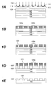
도 1A-E는 본 발명에 따른 포토리소그래피 패턴 형성을 위한 공정 흐름을 나타낸다.
도 2-6은 실시예의 포토레지스트 조성물에 대한 콘트라스트 곡선이다.
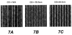
도 7A-C는 실시예의 포토레지스트 조성물을 사용하여 형성된 패턴의 SEM 현미경사진이다.1A-E illustrate a process flow for forming a photolithography pattern according to the present invention.
2-6 are contrast curves for the photoresist compositions of the Examples.
7A-C are SEM micrographs of patterns formed using the photoresist compositions of the examples.
포토레지스트 조성물Photoresist composition
본 발명의 바람직한 포토레지스트 조성물은 네가티브 톤 현상 공정에서 매우 미세한 패턴을 형성하는데 사용되는 경우, 통상의 포지티브-톤 기술에 비해 패턴 붕괴의 제거 또는 감소 및 상부 손실 감소를 제공할 수 있다. 바람직한 포토레지스트 조성물은 초점 허용범위(focus latitude) 및 노광 허용범위(exposure latitude) 개선, 라인 및 접촉에서 기하학적으로 균일한 레지스트 패턴, 및 결함 감소를 추가로 제공할 수 있다. 이들 이점들은 건식 리소그래피(dry lithography) 또는 침지 리소그래피(immersion lithography) 공정에 본 원에 기재된 조성물을 사용하는 경우 이뤄질 수 있다.
Preferred photoresist compositions of the present invention, when used to form very fine patterns in negative tone development processes, can provide removal or reduction of pattern collapse and reduction of top loss as compared to conventional positive-tone techniques. Preferred photoresist compositions can further provide focus latitude and exposure latitude improvements, geometrically uniform resist patterns in lines and contacts, and defect reduction. These advantages can be achieved when using the compositions described herein in a dry lithography or immersion lithography process.
A. 매트릭스 폴리머A. Matrix Polymer
포토레지스트 조성물은 매트릭스 코폴리머를 포함한다. 매트릭스 코폴리머는 포토레지스트 조성물층의 일부로서 소프트베이킹(softbake), 활성화 조사선에 노광 및 노광후 베이킹 후에 포토애시드 발생제로부터 발생된 산과 반응함으로써 유기 현상제에서의 용해도 변화를 겪는다. 매트릭스 코폴리머는 아세탈기 및 환 구조를 가지는 부분을 포함하는 모노머로부터 형성된 제1 단위를 포함한다. 아세탈기의 특징인, 두개의 산소 원자 및 이들 산소 원자에 연결된 제2 탄소원자("아세탈 제2 탄소 원자")는 환 구조의 일부를 형성한다. 연결된 아세탈 제2 탄소 원자는 환 구조에 펜던트된 두 기의 형태를 취할 수 있거나, 아세탈 제2 탄소 원자와 함께, 환 구조의 형태를 취할 수 있는 구조이다. 아세탈 제2 탄소 원자는 펜던트 기(들)와 함께 산 불안정성이고, 활성화 조사선 및 열 처리에 노출시 포토애시드-촉진 탈보호 반응을 겪는다. 아세탈 제2 탄소 원자 및 펜던트 기(들)의 절단으로 전자의 아세탈 산소 원자를 가지는 하이드록시 기가 형성될 것으로 판단된다. 이는 코폴리머가 레지스트층을 형상하기 위해 사용된 유기 용매에 덜 가용성이게 하여 네가티브형 이미지를 형성하도록 만든다.The photoresist composition comprises a matrix copolymer. The matrix copolymer undergoes a change in solubility in the organic developer by reacting with the acid generated from the photoacid generator after softbake, exposure to activated radiation, and post-exposure baking as part of the photoresist composition layer. The matrix copolymer comprises a first unit formed from a monomer comprising a portion having an acetal group and a ring structure. Two oxygen atoms and a second carbon atom connected to these oxygen atoms (“acetal second carbon atoms”), which are characteristic of acetal groups, form part of the ring structure. The linked acetal second carbon atom may take the form of two groups pendant to the ring structure, or together with the acetal second carbon atom, may take the form of a ring structure. Acetal second carbon atoms, together with pendant group (s), are acid labile and undergo a photoacid-promoted deprotection reaction upon exposure to activating radiation and heat treatment. It is believed that the cleavage of the acetal second carbon atom and pendant group (s) will form a hydroxy group having an acetal oxygen atom of the electron. This makes the copolymer less soluble in the organic solvent used to shape the resist layer to form a negative image.
더욱 구체적으로, 모노머는 중합성 작용기; 및 하기 화학식 (I) 또는 화학식 (II)의 제1 부분을 포함한다:More specifically, the monomers may include polymerizable functional groups; And a first portion of formula (I) or formula (II):


상기 식에서,Where
R1 및 R2는 독립적으로 (C1-C10), 바람직하게는 (C1-C6) 선형, 분지형 및 환형 유기 기로부터 선택되거나, 또는 함께, 임의로 환을 형성하며;R 1 and R 2 is independently selected from (C 1 -C 10 ), preferably (C 1 -C 6 ) linear, branched and cyclic organic groups, or together, optionally forms a ring;
a 또는 b중 하나는 1이고, a 또는 b중 다른 하나는 1 또는 2이며;one of a or b is 1 and the other of a or b is 1 or 2;
R3 및 R4는 독립적으로 (C1-C10), 바람직하게는 (C1-C6) 선형, 분지형 및 환형 유기 기로부터 선택되거나, 또는 함께, 임의로 환을 형성하며;R 3 and R 4 is independently selected from (C 1 -C 10 ), preferably (C 1 -C 6 ) linear, branched and cyclic organic groups, or together, optionally forms a ring;
c 또는 d중 하나는 1이고, c 또는 d중 다른 하나는 1 또는 2이다.one of c or d is 1 and the other of c or d is 1 or 2.
R1, R2, R3 및 R4는, 예를 들어 (C1-C10), 바람직하게는 (C1-C6), 탄화수소, 예컨대 (C1-C6)알킬 또는 (C4-C7)사이클로알킬; (C1-C10)알콕시, (C1-C10)알킬카보닐, (C1-C10)알콕시카보닐, (C1-C10)알킬카보닐옥시, 알킬아민, 알킬황 함유 물질 등일 수 있다. R1 및 R2 또는 R3 및 R4가 함께, 환을 형성하는 경우, 이 환은 전형적으로 C4-C6 사이클로알칸이다. R1, R2, R3 및 R4 기는 임의로 치환될 수 있으며, 즉 하나 이상의 수소원자가 다른 원자나 기로 대체될 수 있다.R 1 , R 2 , R 3 and R 4 is for example (C 1 -C 10 ), preferably (C 1 -C 6 ), a hydrocarbon such as (C 1 -C 6 ) alkyl or (C 4 -C 7 ) cycloalkyl; (C 1 -C 10 ) alkoxy, (C 1 -C 10 ) alkylcarbonyl, (C 1 -C 10 ) alkoxycarbonyl, (C 1 -C 10 ) alkylcarbonyloxy, alkylamines, alkylsulfur containing materials And the like. R 1 and R 2 or R 3 and When R 4 together form a ring, this ring is typically C 4 -C 6 cycloalkane. R 1 , R 2 , R 3 and The R 4 group may be optionally substituted, ie one or more hydrogen atoms may be replaced with another atom or group.
모노머는 바람직하게는 제1 부분에 부착된 락톤, 사이클릭 에테르 또는 사이클릭 알칸이며, 예를 들어, 제1 부분은 락톤, 사이클릭 에테르 또는 사이클릭 알칸에 펜던트되거나 융합된다. 바람직한 락톤은 5-원 환 구조를 갖는 것으로부터 선택된다. 바람직한 사이클릭 에테르는 5- 및 6-원 환 구조를 갖는 것으로부터 선택된다. 바람직한 사이클릭 알칸은 6-원 환 구조를 갖는 것으로부터 선택된다. 락톤, 사이클릭 에테르 또는 사이클릭 알칸은 전형적으로 중합성 기에 직접 결합되나, 임의로는 스페이서(spacer) 단위를 통해 중합성 기에 결합될 수 있으며, 스페이서 단위는 예를 들어 임의로 -O-, -S-, -COO- 및 -COONR5-(여기에서, R5는 수소 및 (C1-C10) 선형, 분지형 및 사이클릭 탄화수소로부터 선택된다) 중에서 선택되는 하나 이상의 연결 부분을 가지는 선형 및 분지형 지방족으로부터 선택된다. R5 탄화수소는 임의로 치환될 수 있다. 락톤, 사이클릭 에테르 또는 사이클릭 알칸이 모노머에 존재하는 경우, 제1 부분은 바람직하게는 락톤, 사이클릭 에테르 또는 사이클릭 알칸을 통해 중합성 기에 간접적으로 결합된다. 제1 부분은 예를 들어, 락톤, 사이클릭 에테르 또는 사이클릭 알칸에 펜던트되거나 융합된 환 구조를 형성할 수 있다. 제1 부분 및 락톤, 사이클릭 에테르 또는 사이클릭 알칸에 적합한 구조는 예를 들어, 당, 예컨대 글루코스 및 프럭토스를 포함하는 천연 탄수화물과 케톤의 반응으로 유도된 것이다. 이러한 물질은 상업적으로 입수가능하다.The monomer is preferably a lactone, cyclic ether or cyclic alkanes attached to the first moiety, for example the first moiety is pendant or fused to the lactone, cyclic ether or cyclic alkanes. Preferred lactones are selected from those having a 5-membered ring structure. Preferred cyclic ethers are selected from those having 5- and 6-membered ring structures. Preferred cyclic alkanes are selected from those having a six-membered ring structure. Lactones, cyclic ethers or cyclic alkanes are typically directly bonded to the polymerizable group, but can optionally be bonded to the polymerizable group via spacer units, the spacer units being optionally optionally -O-, -S- , -COO- and -COONR 5 -wherein R 5 is selected from hydrogen and (C 1 -C 10 ) linear, branched and cyclic hydrocarbons, linear and branched with one or more linking moieties Selected from aliphatic groups. R 5 hydrocarbons may be optionally substituted. When lactones, cyclic ethers or cyclic alkanes are present in the monomer, the first part is preferably indirectly bonded to the polymerizable group via lactones, cyclic ethers or cyclic alkanes. The first portion may form a ring structure pendant or fused to, for example, lactones, cyclic ethers or cyclic alkanes. Suitable structures for the first moiety and lactones, cyclic ethers or cyclic alkanes are those derived from the reaction of ketones with natural carbohydrates including, for example, sugars such as glucose and fructose. Such materials are commercially available.
모노머는 하나 이상의 상술된 화학식 (I) 또는 화학식 (II)의 추가의 부분을 더 포함할 수 있으며, 제1 및 상기 추가 부분은 동일하거나 상이하다. 상기 추가 부분이 존재하는 경우, 모노머는 전형적으로 또한 상술된 락톤, 사이클릭 에테르 또는 사이클릭 알칸을 포함할 것이다. 제1 및 추가 부분은 모노머에 다양한 구조로 존재할 수 있다. 예를 들어, 제1 및 제2 부분의 경우, 제1 및 제2 부분중 어느 한 부분은 상술된 바와 같이 락톤, 사이클릭 에테르 또는 사이클릭 알칸에 융합될 수 있고, 제1 및 제2 부분중 다른 부분은 상술된 바와 같이 락톤, 사이클릭 에테르 또는 사이클릭 알칸에 펜던트될 수 있거나, 또는 제1 및 제2 부분 둘다가 락톤, 사이클릭 에테르 또는 사이클릭 알칸에 융합되거나 펜던트될 수 있다. The monomer may further comprise one or more additional portions of the above-mentioned formula (I) or formula (II), wherein the first and the further portions are the same or different. If such additional moieties are present, the monomers will typically also include the lactones, cyclic ethers or cyclic alkanes described above. The first and additional moieties may be present in the monomer in various structures. For example, for the first and second portions, either one of the first and second portions can be fused to lactones, cyclic ethers or cyclic alkanes as described above, and among the first and second portions The other moiety may be pendant to lactones, cyclic ethers or cyclic alkanes as described above, or both the first and second moieties may be fused or pendant to lactones, cyclic ethers or cyclic alkanes.
모노머내 중합성 작용기는, 예를 들어, (메트)아크릴레이트, 비닐 및 비방향족 사이클릭 올레핀(엔도사이클릭 이중결합), 예컨대 노보넨, 예를 들면 하기 화학식 (P-A), (P-B) 및 (P-C)의 것으로부터 선택된다: The polymerizable functional groups in the monomer are, for example, (meth) acrylates, vinyl and non-aromatic cyclic olefins (endocyclic double bonds) such as norbornene, for example the following formulas (PA), (PB) and ( PC) is selected from:


상기 식에서.In the above formula.
R6은 수소 및 C1-C3 알킬로부터 선택되고;R 6 is selected from hydrogen and C 1 -C 3 alkyl;
R7은 수소 및 C1-C3 알킬로부터 선택되며;R 7 is selected from hydrogen and C 1 -C 3 alkyl;
m은 0 내지 3의 정수이다.m is an integer of 0-3.
R6은 임의로 치환될 수 있으며, 즉 하나 이상의 수소원자가 할로겐, 예컨대 불소로 대체될 수 있다. 바람직하게, 모노머의 중합성 기 및 다른 모노머 단위는 화학식 (P-A)의 (메트)아크릴레이트 기이다. R 6 may be optionally substituted, ie one or more hydrogen atoms may be replaced with halogen such as fluorine. Preferably, the polymerizable group and other monomer units of the monomer are (meth) acrylate groups of formula (PA).
화학식 I 또는 II의 적절한 모노머는, 예를 들어, 다음을 들 수 있으나, 이들로 제한되지는 않는다:Suitable monomers of formula (I) or (II) include, but are not limited to, for example:


특정 중합성 기가 상기 모노머로 예시되나, 다른 중합성 기, 예컨대 상술된 화학식 (P-A), (P-B) 및 (P-C)의 것이 사용될 수 있음은 자명하다.Specific polymerizable groups are exemplified by the monomers, but other polymerizable groups such as those described above Obviously, those of the formulas (PA), (PB) and (PC) can be used.
상술된 제1 단위외에, 매트릭스 코폴리머는 하나 이상의 추가의 단위를 포함한다. 전형적으로, 추가의 단위는 제1 모노머에 사용된 것과 동일한 중합성 기를 포함할 것이나, 동일한 폴리머 백본중에 상이한 중합성 기, 예를 들어, 상술된 화학식 (P-A), (P-B) 및/또는 (P-C)의 것을 포함할 수도 있다. 코폴리머에 적합한 추가의 모노머 단위로는, 예를 들어, 하나 이상의 하기 단위들을 들 수 있다: 제1 단위와 상이한 화학식 (I) 또는 (II)의 부분을 포함하는 모노머로부터 형성된 모노머 단위; 에테르, 락톤 또는 에스테르를 포함하는 모노머 단위, 예컨대 2-메틸아크릴산 테트라하이드로푸란-3-일 에스테르, 2-메틸아크릴산 2-옥소-테트라하이드로푸란-3-일 에스테르, 2-메틸아크릴산 5-옥소-테트라하이드로푸란-3-일 에스테르, 2-메틸아크릴산 3-옥소-4,10-디옥사트리사이클로 [5.2.1.02,6] 데크-8-일 에스테르, 2-메틸아크릴산 3-옥소-4-옥사트리사이클로 [5.2.1.02,6] 데크-8-일 에스테르, 2-메틸아크릴산 5-옥소-4-옥사트리사이클로 [4.2.1.03,7] 논-2-일옥시카보닐메틸 에스테르, 아크릴산 3-옥소-4-옥사트리사이클로 [5.2.1.02,6] 데크-8-일 에스테르, 및 2-메틸아크릴산 5-옥소-4-옥사트리사이클로 [4.2.1.03,7] 논-2-일 에스테르, 및 2-메틸아크릴산 테트라하이드로푸란-3-일 에스테르; 극성기, 예컨대 알콜 및 불소화 알콜을 가지는 모노머 단위, 예컨대 2-메틸아크릴산 3-하이드록시-아다만탄-1-일 에스테르, 2-메틸아크릴산 2-하이드록시-에틸 에스테르, 6-비닐-나프탈렌-2-올, 2-메틸아크릴산 3,5-디하이드록시-아다만탄-1-일 에스테르, 2-메틸아크릴산 6-(3,3,3-트리플루오로-2-하이드록시-2-트리플루오로메틸프로필)-비사이클로[2.2.1]헵트-2-일 및 2-비사이클로 [2.2.1] 헵트-5-엔-2-일메틸-1,1,1,3,3,3-헥사플루오로-프로판-2-올; 절단후 카복실산 기를 형성하는 산 불안정성 부분 이외의 산 불안정성 부분을 가지는 모노머 단위, 예컨대 2-메틸아크릴산 2-(1-에톡시-에톡시)-에틸 에스테르, 2-메틸아크릴산 2-에톡시메톡시-에틸 에스테르, 2-메틸아크릴산 2-메톡시메톡시-에틸 에스테르, 2-(1-에톡시-에톡시)-6-비닐-나프탈렌, 2-에톡시메톡시-6-비닐-나프탈렌, 및 2-메톡시메톡시-6-비닐-나프탈렌.In addition to the first unit described above, the matrix copolymer comprises one or more additional units. Typically the additional unit will comprise the same polymerizable groups as used for the first monomer, but different polymerizable groups in the same polymer backbone, for example the formulas (PA), (PB) and / or (PC) described above ) May be included. Further monomer units suitable for the copolymer include, for example, one or more of the following units: monomer units formed from monomers comprising portions of formula (I) or (II) different from the first unit; Monomer units comprising ethers, lactones or esters such as 2-methylacrylic acid tetrahydrofuran-3-yl ester, 2-methylacrylic acid 2-oxo-tetrahydrofuran-3-yl ester, 2-methylacrylic acid 5-oxo- Tetrahydrofuran-3-yl ester, 2-methylacrylic acid 3-oxo-4,10-dioxatricyclo [5.2.1.02,6] Deck-8-yl ester, 2-methylacrylic acid 3-oxo-4-oxa Tricyclo [5.2.1.02,6] deck-8-yl ester, 2-methylacrylic acid 5-oxo-4-oxatricyclo [4.2.1.03,7] non-2-yloxycarbonylmethyl ester, acrylic acid 3- Oxo-4-oxatricyclo [5.2.1.02,6] deck-8-yl ester, and 2-methylacrylic acid 5-oxo-4-oxatricyclo [4.2.1.03,7] non-2-yl ester, and 2-methylacrylic acid tetrahydrofuran-3-yl ester; Monomer units having polar groups such as alcohols and fluorinated alcohols such as 2-methylacrylic acid 3-hydroxy-adamantan-1-yl ester, 2-methylacrylic acid 2-hydroxy-ethyl ester, 6-vinyl-naphthalene-2 -Ol, 2-methylacrylic acid 3,5-dihydroxy-adamantan-1-yl ester, 2-methylacrylic acid 6- (3,3,3-trifluoro-2-hydroxy-2-trifluoro Chloromethyl) -bicyclo [2.2.1] hept-2-yl and 2-bicyclo [2.2.1] hept-5-en-2-ylmethyl-1,1,1,3,3,3- Hexafluoro-propan-2-ol; Monomer units having acid labile moieties other than the acid labile moieties that form carboxylic acid groups after cleavage, such as 2-methylacrylic acid 2- (1-ethoxy-ethoxy) -ethyl ester, 2-methylacrylic acid 2-ethoxymethoxy- Ethyl ester, 2-methylacrylic acid 2-methoxymethoxy-ethyl ester, 2- (1-ethoxy-ethoxy) -6-vinyl-naphthalene, 2-ethoxymethoxy-6-vinyl-naphthalene, and 2 -Methoxymethoxy-6-vinyl-naphthalene.
코폴리머의 제1 단위 및 추가의 단위는 절단에 따라 카복실산 기를 형성하는 산 절단성 기를 함유하지 않으며, 따라서 매트릭스 코폴리머는 이러한 카복실산-형성 산 절단성 기를 함유하지 않는다. 이같은 전형적인 산 절단성 기에는 삼급 비사이클릭 알킬 탄소, 예컨대 t-부틸, 또는 매트릭스 폴리머의 에스테르에 있는 카복실 산소에 공유결합된 삼급 지환식 탄소, 예컨대 메틸아다만틸 또는 에틸펜실을 가지는 에스테르 기를 포함한다. 이러한 기는 통상 193 nm 화학증폭형 포토레지스트에 사용된다. 상술한 바와 같이, 레지스트 현상시 매트릭스 폴리머내에 카복실산 기가 고수준으로 존재하면 패턴 붕괴에 이를 수 있다. 이들 산 절단성 기가 없기 때문에, 본 발명의 포토레지스트 조성물은 전형적으로 포지티브 톤 현상 처리에 통상 사용되는 수성 염기 현상제에서 포지티브 톤 콘트라스트를 나타내지 않는다. 이같은 수성 염기 현상제로는, 예를 들어, 사급 수산화암모늄 용액, 예컨대 테트라-알킬 암모늄 하이드록사이드 용액, 예컨대 테트라메틸 암모늄 하이드록사이드(TMAH) 용액, 전형적으로 0.26N 테트라메틸암모늄 하이드록사이드를 들 수 있다. 따라서, 카복실산-유도 산 절단성 기를 가지는 매트릭스 폴리머를 포함하는 공지 포지티브형 레지스트 시스템에 비해, 본 발명의 포토레지스트 조성물의 노광 영역은 노광후 베이킹된 다음, 수성 염기 현상제에 실질적으로 불용성이다. 벌키한 산 불안정성 기, 예를 들어, 193 nm 포토레지스트 폴리머에 통상 사용되는 삼급 알킬 에스테르 불안정성 기, 예컨대 알킬 아다만틸 기는 노광전 레지스트 층에 비해 상당한 두께 손실 및/또는 에칭 손실에 기여할 수 있다.The first and further units of the copolymer do not contain acid cleavable groups that form carboxylic acid groups upon cleavage and therefore the matrix copolymer does not contain such carboxylic acid-forming acid cleavable groups. Such typical acid cleavable groups include tertiary bicyclic alkyl carbons such as t-butyl, or ester groups having tertiary alicyclic carbons covalently bonded to carboxyl oxygen in esters of the matrix polymer, such as methyladamantyl or ethylpenyl do. Such groups are commonly used in 193 nm chemically amplified photoresists. As described above, the presence of high levels of carboxylic acid groups in the matrix polymer during resist development can lead to pattern collapse. Due to the absence of these acid cleavable groups, the photoresist compositions of the present invention typically exhibit no positive tone contrast in aqueous base developers commonly used in positive tone development treatments. Such aqueous base developers include, for example, quaternary ammonium hydroxide solutions such as tetra-alkyl ammonium hydroxide solutions such as tetramethyl ammonium hydroxide (TMAH) solutions, typically 0.26N tetramethylammonium hydroxide. Can be. Thus, compared to known positive resist systems comprising matrix polymers having carboxylic acid-derived acid cleavable groups, the exposed areas of the photoresist compositions of the present invention are post-exposure baked and then substantially insoluble in aqueous base developers. Bulky acid labile groups, such as tertiary alkyl ester labile groups commonly used in 193 nm photoresist polymers, such as alkyl adamantyl groups, can contribute to significant thickness loss and / or etch loss compared to the pre-exposure resist layer.
서브-200 nm 파장, 예컨대 193 nm에서의 이미지화를 위해, 매트릭스 폴리머는 전형적으로 페닐, 벤질 또는 조사선을 상당량 흡수하는 다른 방향족 기를 실질적으로 함유하지 않는다(예를 들면 15 몰% 미만). 코폴리머는 헤테로원자, 특히 산소 및/또는 황을 가지는 반복 단위, 예를 들어, 폴리머 백본에 융합된 복소지환식 단위; 예컨대 노보넨의 중합으로 제공되는 융합된 탄소 지환식 단위; 및 하나 이상의 헤테로원자(예를 들면, 산소 또는 황)-함유 기, 예를 들어, 하이드록시 나프틸 기로 치환된 탄소환식 아릴 단위로부터 선택된 하나 이상을 함유할 수 있다.For imaging at sub-200 nm wavelengths, such as 193 nm, the matrix polymer typically contains substantially no phenyl, benzyl or other aromatic groups that absorb significant amounts of radiation (eg less than 15 mol%). The copolymers may be heterocyclic, in particular heterocyclic units having oxygen and / or sulfur, such as heterocyclic units fused to the polymer backbone; Fused carbon alicyclic units provided for example by the polymerization of norbornene; And carbocyclic aryl units substituted with one or more heteroatoms (eg, oxygen or sulfur) -containing groups, such as hydroxy naphthyl groups.
매트릭스 폴리머의 중량평균분자량 Mw은 전형적으로 100,000 미만, 예를 들어, 5000 내지 100,000, 더욱 전형적으로 5000 내지 15,000이다. 적합한 매트릭스 폴리머는 상업적으로 입수가능한 출발물질을 사용하여 당업자가 용이하게 제조할 수 있다. 매트릭스 폴리머는 소정 두께의 균일한 코팅을 제공하기에 충분한 양으로 레지스트 조성물에 존재한다. 전형적으로, 매트릭스 폴리머는 조성물 내에 레지스트 조성물의 총 고체 기준으로 70 내지 95 wt%의 양으로 존재한다.
The weight average molecular weight M w of the matrix polymer is typically less than 100,000, for example 5000 to 100,000, more typically 5000 to 15,000. Suitable matrix polymers can be readily prepared by those skilled in the art using commercially available starting materials. The matrix polymer is present in the resist composition in an amount sufficient to provide a uniform coating of the desired thickness. Typically, the matrix polymer is present in the composition in an amount of 70 to 95 wt%, based on the total solids of the resist composition.
B. 포토애시드 발생제B. Photoacid Generator
감광성 조성물은 활성화 조사선에 노광시 조성물의 코팅층에 잠상(latent image)을 생성하기에 충분한 양으로 사용되는 포토애시드 발생제(PAG)를 추가로 포함한다. 예를 들면, 포토애시드 발생제는 포토레지스트 조성물의 총 고체분의 약 1 내지 20 wt%의 양으로 적절히 존재한다. 전형적으로, 화학증폭형 레지스트에는 광활성 성분이 더 적은 것이 적합할 것이다.The photosensitive composition further comprises a photoacid generator (PAG) used in an amount sufficient to produce a latent image in the coating layer of the composition upon exposure to activating radiation. For example, the photoacid generator is suitably present in an amount of about 1 to 20 wt% of the total solids of the photoresist composition. Typically, less photoactive components will be suitable for chemically amplified resists.
적합한 PAG는 화학증폭형 포토레지스트 업계에 공지되었으며, 예를 들어 오늄염, 예를 들면, 트리페닐설포늄 트리플루오로메탄설포네이트, (p-tert-부톡시페닐)디페닐설포늄 트리플루오로메탄설포네이트, 트리스(p-tert-부톡시페닐)설포늄 트리플루오로메탄설포네이트, 트리페닐설포늄 p-톨루엔설포네이트; 니트로벤질 유도체, 예를 들어, 2-니트로벤질 p-톨루엔설포네이트, 2,6-디니트로벤질 p-톨루엔설포네이트, 및 2,4-디니트로벤질 p-톨루엔설포네이트; 설폰산 에스테르, 예를 들어, 1,2,3-트리스(메탄설포닐옥시)벤젠, 1,2,3-트리스(트리플루오로메탄설포닐옥시)벤젠, 및 1,2,3-트리스(p-톨루엔설포닐옥시)벤젠; 디아조메탄 유도체, 예를 들어, 비스(벤젠설포닐)디아조메탄, 비스(p-톨루엔설포닐)디아조메탄; 글리옥심 유도체, 예를 들어, 비스-O-(p-톨루엔설포닐)-α-디메틸글리옥심, 및 비스-O-(n-부탄설포닐)-α-디메틸글리옥심; N-하이드록시이미드 화합물의 설폰산 에스테르 유도체, 예를 들어, N-하이드록시숙신이미드 메탄설폰산 에스테르, N-하이드록시숙신이미드 트리플루오로메탄설폰산 에스테르; 및 할로겐-함유 트리아진 화합물, 예를 들어, 2-(4-메톡시페닐)-4,6-비스(트리클로로메틸)-1,3,5-트리아진 및 2-(4-메톡시나프틸)-4,6-비스(트리클로로메틸)-1,3,5-트리아진을 포함한다. 하나 이상의 상기 PAG가 사용될 수 있다.
Suitable PAGs are known in the chemically amplified photoresist art, for example onium salts such as triphenylsulfonium trifluoromethanesulfonate, (p-tert-butoxyphenyl) diphenylsulfonium trifluoro Methanesulfonate, tris (p-tert-butoxyphenyl) sulfonium trifluoromethanesulfonate, triphenylsulfonium p-toluenesulfonate; Nitrobenzyl derivatives such as 2-nitrobenzyl p-toluenesulfonate, 2,6-dinitrobenzyl p-toluenesulfonate, and 2,4-dinitrobenzyl p-toluenesulfonate; Sulfonic acid esters such as 1,2,3-tris (methanesulfonyloxy) benzene, 1,2,3-tris (trifluoromethanesulfonyloxy) benzene, and 1,2,3-tris ( p-toluenesulfonyloxy) benzene; Diazomethane derivatives such as bis (benzenesulfonyl) diazomethane, bis (p-toluenesulfonyl) diazomethane; Glyoxime derivatives such as bis-O- (p-toluenesulfonyl) -α-dimethylglyoxime, and bis-O- (n-butanesulfonyl) -α-dimethylglyoxime; Sulfonic acid ester derivatives of N-hydroxyimide compounds, for example N-hydroxysuccinimide methanesulfonic acid ester, N-hydroxysuccinimide trifluoromethanesulfonic acid ester; And halogen-containing triazine compounds such as 2- (4-methoxyphenyl) -4,6-bis (trichloromethyl) -1,3,5-triazine and 2- (4-methoxynaph Til) -4,6-bis (trichloromethyl) -1,3,5-triazine. One or more of the PAGs can be used.
C. 용매C. Solvent
본 발명의 포토레지스트 조성물에 적합한 용매로는, 예를 들어 2-메톡시에틸 에테르(디글림), 에틸렌 글리콜 모노메틸 에테르 및 프로필렌 글리콜 모노메틸 에테르와 같은 글리콜 에테르; 프로필렌 글리콜 모노메틸 에테르 아세테이트; 메틸 락테이트 및 에틸 락테이트와 같은 락테이트; 메틸 프로피오네이트, 에틸 프로피오네이트, 에틸 에톡시 프로피오네이트 및 메틸 2-하이드록시 이소부티레이트와 같은 프로피오네이트; 메틸 셀로솔브 아세테이트와 같은 셀로솔브(Cellosolve) 에스테르; 톨루엔 및 크실렌과 같은 방향족 탄화수소; 및 메틸에틸 케톤, 사이클로헥사논 및 2-헵타논과 같은 케톤이 포함된다. 상술된 2, 3 또는 그 이상의 용매의 용매 블렌드도 적합하다. 용매는 전형적으로, 포토레지스트 조성물의 고체 함량의 90 내지 99 wt%, 더욱 전형적으로 95 내지 98 wt%의 양으로 조성물중에 존재한다.
Suitable solvents for the photoresist composition of the present invention include, for example, glycol ethers such as 2-methoxyethyl ether (diglyme), ethylene glycol monomethyl ether and propylene glycol monomethyl ether; Propylene glycol monomethyl ether acetate; Lactates such as methyl lactate and ethyl lactate; Propionates such as methyl propionate, ethyl propionate, ethyl ethoxy propionate and methyl 2-hydroxy isobutyrate; Cellosolve esters such as methyl cellosolve acetate; Aromatic hydrocarbons such as toluene and xylene; And ketones such as methylethyl ketone, cyclohexanone and 2-heptanone. Solvent blends of the two, three or more solvents described above are also suitable. The solvent is typically present in the composition in an amount of 90 to 99 wt%, more typically 95 to 98 wt% of the solids content of the photoresist composition.
D. 기타 성분D. Other Ingredients
포토레지스트 조성물은 또한 기타 임의 물질을 포함할 수 있다. 예를 들어, 조성물은 화학선 염료, 조영제, 줄무늬 방지제(anti-striation agent), 가소제, 속도 증강제(speed enhancer), 감광제 등중의 하나 이상을 포함한다. 이러한 임의의 첨가제는 사용될 경우, 전형적으로 낮은 농도, 예컨대 포토레지스트 조성물의 총 고체를 기준으로 5 내지 30 wt%의 양으로 포토레지스트 조성물 내에 존재할 것이다. The photoresist composition may also include any other material. For example, the composition includes one or more of actinic dyes, contrast agents, anti-striation agents, plasticizers, speed enhancers, photosensitizers, and the like. If such optional additives are used, they will typically be present in the photoresist composition in low concentrations such as 5-30 wt% based on the total solids of the photoresist composition.
본 발명의 레지스트 조성물에 바람직한 임의 첨가제는 첨가 염기로서, 예를 들면, 현상 레지스트 릴리프 이미지의 해상도를 높일 수 있는 카프로락탐이다. 그밖의 적합한 염기성 첨가제로는 알킬 아민, 예컨대 트리프로필아민 및 도데실아민, 아릴 아민, 예컨대 디페닐아민, 트리페닐아민, 아미노페놀, 2-(4-아미노페닐)-2-(4-하이드록시페닐)프로판 등을 들 수 있다. 첨가 염기는 비교적 소량, 예를 들어, 포토레지스트 조성물의 총 고체를 기준으로 0.01 내지 5 wt%, 바람직하게는 0.1 내지 2 wt%의 양으로 적절히 사용된다. Preferred optional additives for the resist composition of the present invention are caprolactams which can increase the resolution of a developing resist relief image, for example, as an added base. Other suitable basic additives include alkyl amines such as tripropylamine and dodecylamine, aryl amines such as diphenylamine, triphenylamine, aminophenols, 2- (4-aminophenyl) -2- (4-hydroxy Phenyl) propane etc. are mentioned. The added base is suitably used in relatively small amounts, for example in amounts of 0.01 to 5 wt%, preferably 0.1 to 2 wt%, based on the total solids of the photoresist composition.
표면활성 폴리머는 레지스트 층상에 톱코트(top-coat) 층을 사용할 필요가 없음으로 해서 침지 리소그패리 공정을 단순화하도록 포토레지스트 제제내에 첨가제로서 임의로 사용될 수 있다. 톱코트 층은 전형적으로 레지스트 성분, 예컨대 포토애시드 발생제가 이미지화 렌즈 표면을 오염시키지 못하도록 사용된다. 포토레지스트 제제에 첨가되는 표면활성 폴리머 첨가제는 비교적 낮은 표면 자유 에너지로 해서 코팅 공정동안 표면으로 이동한다. 표면활성 폴리머 첨가제는 표면활성 폴리머가 표면으로 이동하도록 매트릭스 폴리머보다 표면 자유 에너지가 낮아야 한다. 표면활성 폴리머 첨가제의 전형적인 표면 자유 에너지는 10 내지 40 mJ/m2이다. 적합한 표면활성 폴리머는 당업계에 알려져 있으며, 예를 들어, [Tsibouklis and Nevell (Advanced Materials, 2003, 15, pp.647-650)]에 개시된 것을 들 수 있다. 적합한 폴리머 첨가제의 예로는 폴리(n-부틸 아크릴레이트), 폴리(n-부틸 메타크릴레이트), 폴리(i-부틸 아크릴레이트), 폴리(i-부틸 메타크릴레이트), 폴리(디에틸 실록산), 폴리(비닐 부티레이트), 폴리테트라하이드로푸란, 폴리(프로필렌 글리콜), 폴리(테트라메틸렌 옥사이드) 및 불소화 폴리머를 들 수 있다. 하나 이상의 첨가제 폴리머는 전형적으로 포토레지스트 조성물중에 비교적 소량이지만 여전히 효과적인 결과를 제공하는 양으로 존재할 수 있다. 첨가제 폴리머의 함량은, 예를 들어, 리소그래피가 건식 또는 침지형 공정인지에 따라 달라진다. 예를 들어, 침지 리소그래피에 대한 첨가제 폴리머의 하한은 일반적으로 레지스트 성분의 누출 예방 필요성에 따라 달라진다. 고도의 첨가제 폴리머 함량은 전형적으로 패턴 붕괴로 이어진다. 하나 이상의 폴리머 첨가제는 전형적으로 본 발명의 조성물중에 포토레지스트 조성물의 총 고체를 기준으로 0.1 내지 10 wt%, 더욱 전형적으로는 1 내지 5 wt%의 양으로 조재한다. 첨가제 폴리머의 중량평균분자량은 전형적으로 400,000 미만, 예를 들어 5000 내지 50,000이다.
Surface active polymers may optionally be used as additives in the photoresist formulation to simplify the immersion lithography process by eliminating the need to use a top-coat layer on the resist layer. Topcoat layers are typically used to prevent resist components, such as photoacid generators, from contaminating the imaging lens surface. Surface active polymer additives added to the photoresist formulation migrate to the surface during the coating process with relatively low surface free energy. The surface active polymer additive must have lower surface free energy than the matrix polymer in order for the surface active polymer to migrate to the surface. Typical surface free energy of the surface active polymer additive is 10 to 40 mJ / m 2 . Suitable surface active polymers are known in the art and include, for example, those disclosed in Tsibouklis and Nevell (Advanced Materials, 2003, 15, pp. 647-650). Examples of suitable polymer additives include poly (n-butyl acrylate), poly (n-butyl methacrylate), poly (i-butyl acrylate), poly (i-butyl methacrylate), poly (diethyl siloxane) , Poly (vinyl butyrate), polytetrahydrofuran, poly (propylene glycol), poly (tetramethylene oxide) and fluorinated polymers. One or more additive polymers may typically be present in the photoresist composition in amounts that are relatively small but still provide effective results. The content of the additive polymer depends, for example, on whether the lithography is a dry or immersed process. For example, the lower limit of the additive polymer for immersion lithography generally depends on the need to prevent leakage of the resist component. Highly additive polymer content typically leads to pattern collapse. One or more polymer additives are typically formulated in an amount of 0.1 to 10 wt%, more typically 1 to 5 wt%, based on the total solids of the photoresist composition in the composition of the present invention. The weight average molecular weight of the additive polymer is typically less than 400,000, for example 5000 to 50,000.
포토레지스트 조성물의 제조Preparation of Photoresist Composition
본 발명에 따라 사용되는 포토레지스트는 공지된 방법에 따라 일반적으로 제조된다. 예를 들어, 본 발명의 포토레지스트 조성물은 포토레지스트 성분을 용매 성분에 용해시킴으로써 제조될 수 있다. 바람직한 포토레지스트의 총 고체 함량은 조성물내 특정 폴리머, 최종층 두께 및 노과 파장과 같은 인자에 따라 달라질 것이다. 전형적으로, 포토레지스트의 고체 함량은 포토레지스트 조성물의 총중량을 기준으로 약 1 내지 10 wt%, 더욱 전형적으로는 약 2 내지 5 wt%로 변한다.
Photoresists used according to the invention are generally prepared according to known methods. For example, the photoresist composition of the present invention can be prepared by dissolving the photoresist component in a solvent component. The total solids content of the preferred photoresist will depend on factors such as the particular polymer in the composition, the final layer thickness and the furnace wavelength. Typically, the solids content of the photoresist varies from about 1 to 10 wt%, more typically about 2 to 5 wt%, based on the total weight of the photoresist composition.
네가티브 톤 현상법Negative tone development
본 발명은 또한 본 발명의 포토레지스트를 사용한 포토레지스트 릴리프 이미지의 형성방법 및 전자 디바이스의 제조방법을 제공한다. 본 발명은 또한 본 발명의 포토레지스트로 코팅된 기판을 포함하는 신규 제품을 제공한다. 이하 본 발명이 네가티브 톤 현상으로 포토리소그래피 패턴을 형성하기 위한 예시 공정 흐름도를 나타내는 도 1A-E를 참조하여 설명된다.The present invention also provides a method of forming a photoresist relief image using the photoresist of the present invention and a method of manufacturing an electronic device. The present invention also provides a novel product comprising a substrate coated with the photoresist of the present invention. DETAILED DESCRIPTION The present invention is described below with reference to FIGS. 1A-E, which illustrate an exemplary process flow diagram for forming a photolithographic pattern with negative tone development.
도 1A는 다양한 층 및 피처를 포함할 수 있는 기판(100)의 횡단면을 도시한 것이다. 기판은 예컨대 실리콘 또는 화합물 반도체(예를 들어, III-V 또는 II-VI)와 같은 반도체, 유리, 석영, 세라믹, 구리 등과 같은 물질일 수 있다. 전형적으로, 기판은 단결정 실리콘 또는 화합물 반도체 웨이퍼와 같은 반도체 웨이퍼이며, 그의 표면상에 형성된 하나 이상의 층 및 패턴화된 피처를 가질 수 있다. 패턴화될 하나 이상의 층(102)이 기판(100) 위에 제공될 수 있다. 임의로는, 예를 들어 기판 물질 내에 트렌치(trenches)를 형성하고자 할 경우, 하부 베이스 기판 물질 자체도 패턴화될 수 있다. 베이스 기판 물질 자체를 패터닝할 경우, 패턴은 기판의 층 내에 형성될 것으로 판단된다.1A illustrates a cross section of a
상기 층은, 하나 이상의 전도층, 예컨대 알루미늄층, 구리층, 몰리브덴층, 탄탈륨층, 티타늄층, 텅스텐층, 이들 금속의 합금층, 니트라이드층 또는 실리사이드층(silicides), 도핑된 무정형 실리콘층 또는 도핑된 폴리실리콘층, 하나 이상의 유전체층, 예컨대 실리콘 옥사이드층, 실리콘 니트라이드층, 실리콘 옥시니트라이드층, 또는 금속 옥사이드층, 단결정 실리콘과 같은 반도체층 및 이들의 조합을 포함할 수 있다. 에칭될 층은 플라즈마-증강 CVD, 저압력 CVD 또는 에피택셜 성장과 같은 화학 증착법(CVD); 스퍼터링 또는 증발과 같은 물리적 증착법(PVD); 또는 일렉트로플레이팅법 등과 같은 다양한 기술로 형성될 수 있다. 에칭될 하나 이상의 층(102)의 특정 두께는 형성될 물질 및 장비에 따라 변경될 것이다.The layer may comprise at least one conductive layer, such as an aluminum layer, a copper layer, a molybdenum layer, a tantalum layer, a titanium layer, a tungsten layer, an alloy layer of these metals, a nitride layer or silicide layers, a doped amorphous silicon layer or Doped polysilicon layers, one or more dielectric layers, such as silicon oxide layers, silicon nitride layers, silicon oxynitride layers, or metal oxide layers, semiconductor layers such as single crystal silicon, and combinations thereof. The layer to be etched may include chemical vapor deposition (CVD) such as plasma-enhanced CVD, low pressure CVD or epitaxial growth; Physical vapor deposition (PVD), such as sputtering or evaporation; Or various techniques such as an electroplating method. The particular thickness of one or
에칭될 특정 층, 필름 두께 및 사용될 포토리소그래피 물질 및 방법에 따라, 층(102) 위에 하드 마스크층(104) 및/또는 바닥 반사방지 코팅(BARC; 106)을 배치하고 그 위에 포토레지스트층(108)이 코팅되는 것이 필요할 수 있다. 하드마스크층(104)은, 예를 들면, 매우 얇은 레지스트층과 함께 에칭될 층이 상당한 에칭 깊이를 필요로 하고/거나 특정 부식제가 레지스트 선택성이 낮은 경우, 그 사용이 필요할 수 있다. 하드마스크층이 사용되는 경우, 형성되는 레지스트 패턴은 하드마스크층으로 이송될 수 있으며, 이는 차례로 하부층(102)을 에칭하는 마스크로 사용될 수 있다. 적합한 하드마스크 물질 및 형성 방법은 본 기술분야에 알려져 있다. 대표적인 물질은, 예를 들면, 텅스텐, 티타늄, 티타늄 니트라이드, 티타늄 옥사이드, 지르코늄 옥사이드, 알루미늄 옥사이드, 알루미늄 옥시니트라이드, 하프늄 옥사이드, 무정형 카본, 실리콘 옥시니트라이드 및 실리콘 니트라이드를 포함한다. 하드마스크층(104)은 단일 또는 복수의 상이한 물질층을 포함할 수 있다. 하드마스크층은 예를 들면, 화학적 또는 물리적 증착기술에 의해 형성될 수 있다.Depending on the particular layer to be etched, the film thickness, and the photolithography material and method to be used, a
기판 및/또는 하부층이 포토레지스트 노광 동안 입사광선의 상당량을 반사하여 형성되는 패턴의 품질에 유해한 영향을 줄 수 있는 경우, 바닥 반사방지 코팅(106)이 필요할 수 있다. 이러한 코팅은 초점 심도, 노출 위도, 라인폭의 균일성 및 CD 조절을 개선할 수 있다. 반사방지 코팅은 일반적으로 레지스트가 심자외선(300 nm 이하), 예를 들면 KrF 엑시머 레이저광(248 nm), ArF 엑시머 레이저광(193 nm)에 노광될 경우 사용된다. 반사방지 코팅(106)은 단일 또는 복수의 상이한 층을 포함할 수 있다. 적합한 반사방지 물질과 제조방법은 당분야에 알려져 있다. 반사방지 물질은, 예를 들면 Rohm and Haas Electronic Materials LLC (Marlborough, MA USA)가 ARTM 상표로 판매하는 제품을 구입할 수 있으며, 예를 들면 ARTM40A 및 ARTM124 반사방지 물질 등이 있다.Bottom
본 원에 기술된 포토레지스트 조성물을 반사방지층(106)(존재한다면) 위의 기판에 적용하여 포토레지스트층(108)을 형성한다. 포토레지스트 조성물을 스핀 코팅, 딥핑, 롤러 코팅 또는 다른 일반적인 코팅방법에 의해 기판에 적용할 수 있다. 이들 중에서 스핀 코팅이 전형적이다. 스핀 코팅에 있어서, 코팅 용액 중의 고체 함량을 조절하여 사용되는 특정한 코팅 장치, 용액의 점도, 코팅 장비의 속도 및 스피닝에 허용되는 시간에 따라 원하는 필름 두께를 제공할 수 있다. 포토레지스트층(108)의 전형적인 두께는 약 500 내지 3000 Å이다.The photoresist composition described herein is applied to a substrate over the antireflective layer 106 (if present) to form a
다음으로, 포토레지스트층을 소프트베이킹하여 층 내의 용매 함량을 최소화하고, 무점착성(tack-free) 코팅을 형성하여 기판에 대한 층의 점착을 개선한다. 소프트베이킹은 핫플레이트 상에서 또는 오븐에서 수행할 수 있으며, 핫플레이트가 전형적이다. 소프트베이킹 시간과 온도는, 예를 들면 포토레지스트의 미립자 물질 및 두께에 따라 달라질 수 있다. 전형적인 소프트베이킹은 약 90 내지 150 ℃의 온도에서 약 30 내지 90초 동안 수행한다.Next, the photoresist layer is softbaked to minimize solvent content in the layer and to form a tack-free coating to improve the adhesion of the layer to the substrate. Softbaking can be performed on a hotplate or in an oven, where hotplates are typical. Softbaking times and temperatures may vary depending on, for example, the particulate material and thickness of the photoresist. Typical softbaking is performed for about 30 to 90 seconds at a temperature of about 90 to 150 ° C.
포토레지스트층(108)은 제1 포토마스크(112)를 통해 활성 조사선 (110)에 노광되어 노광된 영역과 노광되지 않은 영역 사이에서 용해도 차를 생성한다. 여기에서 조성물을 활성화하는 조사선에 포토레지스트 조성물을 노광한다는 것은 조사선이 포토레지스트 조성물에서 잠상을 형성할 수 있음을 나타낸다. 포토마스크는 예시된 바와 같은 포지티브 활성 물질의 후속 현상 단계에서 각각 남는 것과 제거되는 레지스트층의 영역에 해당하는 광학적으로 투명한 영역과 광학적으로 불투명한 영역(113, 114)을 가진다. 노광 파장은 전형적으로 서브-400 nm, 서브-300 nm 또는 서브-200 nm이며, 248 nm 및 193 nm가 전형적이다. 이 방법은 침지 또는 건식(비침지) 리소그래피 방법에 사용될 수 있다. 노광 에너지는 노광 장비 및 광감성 조성물의 성분에 따라 약 10 내지 80 mJ/cm2이다.The
도 1B에 나타낸 바와 같이, 노광된 레지스트층은 노광되지 않은 영역과 노광된 영역(108a, 108b)으로 구성된다. 포토레지스트층(108)을 노광한 후, 노광후 베이킹(PEB)을 수행한다. PEB는, 예를 들면 핫플레이트 또는 오븐에서 수행할 수 있다. PEB의 조건은, 예를 들면 특정 포토레지스트 조성물 및 층 두께에 따라 달라질 수 있다. PEB는 전형적으로 약 80 내지 150 ℃의 온도에서 30 내지 90초 동안 수행한다.As shown in Fig. 1B, the exposed resist layer is composed of an unexposed region and exposed
다음으로, 노광된 포토레지스트층을 현상하여 도 1C에 나타낸 바와 같이 노광되지 않은 영역(108a)을 제거하고, 노광된 영역(108b)을 남겨 레지스트 패턴을 형성한다. 현상제는 전형적으로 유기 현상제, 예를 들면 케톤, 에스테르, 에테르, 탄화수소 및 이들의 혼합물에서 선택되는 용매이다. 적합한 케톤 용매는, 예를 들면 아세톤, 2-헥사논, 5-메틸-2-헥사논, 2-헵타논, 4-헵타논, 1-옥타논, 2-옥타논, 1-노나논, 2-노나논, 디이소부틸 케톤, 사이클로헥사논, 메틸사이클로헥사논, 페닐아세톤, 메틸 에틸 케톤 및 메틸 이소부틸 케톤 등이다. 적합한 에스테르 용매는, 예를 들면 메틸 아세테이트, 부틸 아세테이트, 에틸 아세테이트, 이소프로필 아세테이트, 아밀 아세테이트, 프로필렌 글리콜 모노메틸 에테르 아세테이트, 에틸렌 글리콜 모노에틸 에테르 아세테이트, 디에틸렌 글리콜 모노부틸 에테르 아세테이트, 디에틸렌 글리콜 모노에틸 에테르 아세테이트, 에틸-3-에톡시프로피오네이트, 3-메톡시부틸 아세테이트, 3-메틸-3-메톡시부틸 아세테이트, 메틸 포르메이트, 에틸 포르메이트, 부틸 포르메이트, 프로필 포르메이트, 에틸 락테이트, 부틸 락테이트 및 프로필 락테이트 등이다. 적합한 에테르 용매는, 예를 들면 디옥산, 테트라하이드로푸란 및 글리콜 에테르 용매, 예를 들면 에틸렌 글리콜 모노메틸 에테르, 프로필렌 글리콜 모노메틸 에테르, 에틸렌 글리콜 모노에틸 에테르, 프로필렌 글리콜 모노에틸 에테르, 디에틸렌 글리콜 모노메틸 에테르, 트리에틸렌 글리콜 모노에틸 에테르 및 메톡시메틸 부탄올 등이다. 적합한 아미드 용매는, 예를 들면 N-메틸-2-피롤리돈, N,N-디메틸아세트아미드 및 N,N-디메틸포름아미드 등이다. 적합한 탄화수소 용매는, 예를 들면 방향족 탄화수소 용매, 예를 들면 톨루엔, 크실렌 등이다. 또한 이 용매들의 혼합물, 또는 1 이상의 열거된 용매와 상기한 용매 이외의 용매 또는 물과의 혼합물을 사용할 수 있다. 이들 중에서 2-헵타논과 5-메틸-2-헥사논이 특히 바람직하다. 다른 적합한 용매로는 포토레지스트 조성물에 사용되는 용매를 사용할 수 있다.Next, the exposed photoresist layer is developed to remove the
용매는 실질적으로 순수물로서, 예를 들면 현상제의 총 중량에 대하여 95 wt%를 초과, 98 wt%를 초과하거나 또는 99 wt%를 초과하는 양으로 존재할 수 있다. 용매의 혼합물을 현상제에서 사용하는 경우에 용매의 끓는점은 바람직하게 유사하다. 현상제의 용매는 전형적으로 현상제의 총 중량에 대하여 50 wt% 내지 100 wt%, 더욱 전형적으로 80 wt% 내지 100 wt%의 양으로 존재한다.The solvent may be substantially pure, for example in an amount greater than 95 wt%, greater than 98 wt% or greater than 99 wt% with respect to the total weight of the developer. The boiling point of the solvents is preferably similar when a mixture of solvents is used in the developer. The solvent of the developer is typically present in an amount of 50 wt% to 100 wt%, more typically 80 wt% to 100 wt%, relative to the total weight of the developer.
현상제 물질은 임의의 첨가제, 예를 들면 포토레지스트와 관련하여 상기한 바와 같은 계면활성제 등을 포함할 수 있다. 이러한 임의의 첨가제는 전형적으로 미량 농도로 존재할 수 있으며, 예를 들면 현상제의 총 중량에 대하여 약 0.01 내지 5 wt%의 양으로 존재한다.The developer material may include any additives such as surfactants as described above in connection with the photoresist and the like. Such optional additives may typically be present in trace concentrations, for example in an amount of about 0.01-5 wt% by weight relative to the total weight of the developer.
현상제는 공지된 방법, 예를 들면 스핀 코팅 또는 퍼들(puddle) 코팅 등에 의해 기판에 적용할 수 있다. 현상시간은 포토레지스트의 노광되지 않은 영역을 제거하는데 효과적인 시간 동안이며, 5 내지 30초가 전형적이다. 현상은 전형적으로 실온에서 수행한다. 현상 과정은 현상 후에 세정 린스의 사용없이 수행할 수 있다. 이와 관련하여, 현상 과정은 잔사가 없는 웨이퍼 표면을 생성하여 추가의 린스 단계를 필요로 하지 않는 것이 확실하다.The developer can be applied to the substrate by known methods, for example spin coating or puddle coating. The development time is for an effective time to remove the unexposed areas of the photoresist, with 5 to 30 seconds being typical. Development is typically carried out at room temperature. The development process can be carried out after the development without the use of a cleaning rinse. In this regard, it is evident that the development process produces a wafer surface free of residue and does not require additional rinse steps.
BARC층(106)은, 존재할 경우, 에칭 마스크로서 레지스트 패턴(108b)을 사용하여 선택적으로 에칭하여 하부 하드마스크층(104)을 노출한다. 이어서, 하드마스크층을 다시 에칭 마스크로서 레지스트 패턴(108b)을 사용하여 선택적으로 에칭하여, 도 1D에 나타낸 바와 같이 패턴화된 BARC와 하드마스크층(106', 104')을 생성한다. BARC층과 하드마스크층을 에칭하는 적합한 에칭 기술과 화학적 방법은 당업계에 알려져 있으며, 예를 들면 이러한 층들의 특정 물질에 따라 달라질 것이다. 반응성 이온 에칭과 같은 드라이에칭 방법이 전형적이다. 다음으로, 레지스트 패턴(108b)과 패턴화된 BARC층(106')을 공지된 방법, 예를 들면 산소 플라즈마 애싱을 사용하여 기판에서 제거한다.
에칭 마스크로서 하드마스크 패턴(104')을 사용하여, 1 이상의 층(102)을 선택적으로 에칭한다. 하위층(102)을 에칭하기에 적합한 에칭 기술과 화학적 방법은 당업계에 알려져 있으며, 반응성 이온 에칭과 같은 드라이에칭 방법이 전형적이다. 패턴화된 하드마스크층(104')은 종래의 방법, 예를 들면 반응성 이온 에칭과 같은 드라이에칭 방법을 사용하여 기판 표면에서 제거할 수 있다. 생성된 구조는 도 1E에 나타낸 바와 같이 에칭된 피처(feature)(102')의 패턴이다. 예시적인 대안 방법에 있어서, 층(102)을 레지스트 패턴(108b)을 사용하여 하드마스크층(104) 없이 직접 패턴화하는 것이 바람직하다. 직접 패턴화를 적용할 것인지는 관련 물질, 레지스트 선택성, 레지스트 패턴 두께 및 패턴 치수 등의 인자에 따라 결정된다.One or
본 발명의 네가티브 톤 현상방법은 상기한 예시적인 방법에 제한되지 않는다. 예를 들면, 본 발명의 포토레지스트 조성물은 접촉홀을 제조하기 위한 네가티브 톤 현상 이중 노광법에서도 사용될 수 있다. 이러한 예시적인 방법은 도 1을 참조로 하여 기술된 방법의 변형이지만, 제1 노광과는 상이한 패턴으로 포토레지스트층의 추가 노광을 사용한다. 이 공정에서는, 포토레지스트층을 제1 노광 단계에서 화학 조사선에 포토마스크를 통해 노광시키다. 포토마스크는 마스크의 불투명 영역을 형성하는 일련의 평행선을 포함한다. 제1 노광 후에, 포토레지스트층의 제2 노광을 제1 포토마스크의 선들과 수직한 방향의 일련의 선들을 포함하는 제2 포토마스크를 통해 수행된다. 얻어진 포토레지스트층은 비노광 영역, 1회 노광된 영역 및 2회 노광된 영역을 포함한다.The negative tone developing method of the present invention is not limited to the exemplary method described above. For example, the photoresist composition of the present invention can also be used in the negative tone development double exposure method for producing contact holes. This exemplary method is a variation of the method described with reference to FIG. 1, but uses additional exposure of the photoresist layer in a pattern different from the first exposure. In this step, the photoresist layer is exposed to the actinic radiation through a photomask in the first exposure step. The photomask includes a series of parallel lines that form the opaque regions of the mask. After the first exposure, a second exposure of the photoresist layer is performed through a second photomask comprising a series of lines in a direction perpendicular to the lines of the first photomask. The obtained photoresist layer includes a non-exposed area, a region exposed once and a region exposed twice.
2차 노광 후에, 포토레지스트층을 노광후 베이킹하고 상기한 바와 같은 현상제를 사용하여 현상한다. 2개 마스크의 선들의 교차점에 해당하는 비노광 영역을 제거하고 레지스트의 1회 및 2회 노광 영역을 남긴다. 생성된 구조를 상기한 바와 같이 패턴화할 수 있으며, 도 1을 참조한다. 이 방법은 특히 전자 디바이스 제조시 접촉홀 형성에 적합하다.
After the secondary exposure, the photoresist layer is post-exposure baked and developed using a developer as described above. The non-exposed areas corresponding to the intersections of the lines of the two masks are removed, leaving one and two exposure areas of the resist. The resulting structure can be patterned as described above, see FIG. 1. This method is particularly suitable for forming contact holes in the manufacture of electronic devices.
매트릭스 폴리머 합성Matrix polymer synthesis
다음 모노머가 하기 실시예에서 코폴리머의 합성에 이용되었다.The following monomers were used for the synthesis of the copolymers in the examples below.

폴리(MAMA/α-GBLMA/MNLMA)의 합성Synthesis of Poly (MAMA / α-GBLMA / MNLMA)
27.48g의 MAMA, 15.96g의 a-GBLMA, 및 6.57g의 MNLMA를 62g의 PGMEA에 용해시켰다. 혼합물을 20분 동안 질소로 버블링하여 탈기시켰다. 콘데서, 질소 주입구 및 기계적인 스터러를 갖춘 500ml 플라스크에 35g의 PGMEA로 채우고, 용액을 80 ℃의 온도로 하였다. 2.0g의 PGMEA에 용해시킨 2.52g의 V601(디메틸-2,2-아조디이소부티레이트)를 플라스크에 채웠다. 모노머 용액을 27.42 mL/h의 속도로 반응기에 공급했다. 1시간 후에, 2.0 g의 PGMEA에 용해시킨 1.26g의 V-601을 반응기에 첨가하고, 모노머 공급(feeding)을 3 시간 더 행하였다. 모노머 공급이 완료된 후, 중합 혼합물을 80 ℃에서 추가로 3 시간동안 교반하였다. 총 7 시간동안의 중합 이후(4시간의 공급 및 3시간의 교반), 중합 혼합물을 상온까지 식혔다. 2.0L의 이소프로필 알콜로 침전시켰다. 여과 후, 폴리머를 건조시키고, 162g의 THF에 다시 용해시키고, 3.2L의 이소프로필 알콜로 재침전시키고, 여과하고, 45 ℃ 진공 오븐에서 48 시간동안 건조시켜서 41.5g(Mw = 6498 and Mw/Mn = 1.62)인 하기의 "폴리머 A"를 제조했다. 27.48 g MAMA, 15.96 g a-GBLMA, and 6.57 g MNLMA were dissolved in 62 g PGMEA. The mixture was degassed by bubbling with nitrogen for 20 minutes. In a condenser, a 500 ml flask equipped with a nitrogen inlet and a mechanical stirrer was charged with 35 g of PGMEA and the solution was brought to a temperature of 80 ° C. The flask was charged with 2.52 g of V601 (dimethyl-2,2-azodiisobutyrate) dissolved in 2.0 g of PGMEA. The monomer solution was fed to the reactor at a rate of 27.42 mL / h. After 1 hour, 1.26 g of V-601 dissolved in 2.0 g of PGMEA was added to the reactor and monomer feeding was further performed for 3 hours. After the monomer feed was complete, the polymerization mixture was stirred at 80 ° C. for an additional 3 hours. After a total of 7 hours of polymerization (4 hours of feeding and 3 hours of stirring), the polymerization mixture was cooled to room temperature. Precipitated with 2.0 L of isopropyl alcohol. After filtration, the polymer was dried, re-dissolved in 162 g THF, reprecipitated with 3.2 L isopropyl alcohol, filtered and dried for 48 h in a 45 ° C. vacuum oven to 41.5 g (Mw = 6498 and Mw / Mn). = 1.62), the following "polymer A" was prepared.

폴리(IPGFMA/a-GBLMA/MNLMA)의 합성Synthesis of Poly (IPGFMA / a-GBLMA / MNLMA)
15.77g의 IPGFMA, 6.54g의 α-GBLMA 및 2.69g의 MNLMA를 31g의 PGMEA에 용해시켰다. 혼합물을 20분 동안 질소로 버블링하여 탈기시켰다. 콘데서, 질소 주입구 및 기계적인 스터러를 갖춘 500ml 플라스크에 35g의 PGMEA로 채우고, 용액을 80 ℃의 온도로 하였다. 1.0g의 PGMEA에 용해시킨 1.03g의 V601(디메틸-2,2-아조다이이소부티레이트)를 플라스크에 채웠다. 모노머 용액을 13.0mL/h의 속도로 반응기에 공급했다. 1시간 후에, 1.0g의 PGMEA에 용해시킨 0.52g의 V-601을 반응기에 첨가하고, 모노머 공급을 3 시간 더 행하였다. 모노머 공급이 완료된 후, 중합 혼합물을 80 ℃에서 추가로 3 시간동안 교반하였다. 총 7 시간동안의 중합(4시간의 공급 및 3시간의 교반) 후, 중합 혼합물을 상온까지 식혔다. 1.0L의 이소프로필 알콜로 침전시켰다. 여과 후, 폴리머를 건조시키고, 52g의 THF에 다시 용해시키고, 1.1L의 이소프로필 알콜로 재침전시키고, 여과하고, 45 ℃ 진공 오븐에서 48 시간동안 건조시켜서 18.5g(Mw = 14378 및 Mw/Mn = 1.75)인 하기의 "폴리머 B"를 제조했다.15.77 g IPGFMA, 6.54 g α-GBLMA and 2.69 g MNLMA were dissolved in 31 g PGMEA. The mixture was degassed by bubbling with nitrogen for 20 minutes. In a condenser, a 500 ml flask equipped with a nitrogen inlet and a mechanical stirrer was charged with 35 g of PGMEA and the solution was brought to a temperature of 80 ° C. The flask was charged with 1.03 g of V601 (dimethyl-2,2-azodiisobutyrate) dissolved in 1.0 g of PGMEA. The monomer solution was fed to the reactor at a rate of 13.0 mL / h. After 1 hour, 0.52 g of V-601 dissolved in 1.0 g of PGMEA was added to the reactor, and monomer feed was further performed for 3 hours. After the monomer feed was complete, the polymerization mixture was stirred at 80 ° C. for an additional 3 hours. After a total of 7 hours of polymerization (4 hours of feeding and 3 hours of stirring), the polymerization mixture was cooled to room temperature. Precipitated with 1.0 L of isopropyl alcohol. After filtration, the polymer is dried, re-dissolved in 52 g of THF, reprecipitated with 1.1 L of isopropyl alcohol, filtered and dried for 48 h in a 45 ° C. vacuum oven to give 18.5 g (Mw = 14378 and Mw / Mn). = 1.75) of the following "Polymer B".

폴리(IPGPMA/α-GBLMA/MNLMA)의 합성Synthesis of Poly (IPGPMA / α-GBLMA / MNLMA)
15.77g의 IPGPMA, 6.54g의 α-GBLMA 및 2.69g의 MNLMA를 31g의 PGMEA에 용해시켰다. 혼합물을 20분 동안 질소로 버블링하여 탈기시켰다. 콘데서, 질소 주입구 및 기계적인 스터러를 갖춘 500ml 플라스크에 18g의 PGMEA로 채우고, 용액을 80 ℃의 온도로 하였다. 1.0g의 PGMEA에 용해시킨 1.03g의 V601(디메틸-2,2-아조디이소부티레이트)를 플라스크에 채웠다. 모노머 용액을 13.0mL/h의 속도로 반응기에 공급했다. 1시간 후에, 1.0g의 PGMEA에 용해시킨 0.52g의 V-601을 반응기에 첨가하고, 모노머 공급을 3 시간 더 행하였다. 모노머 공급이 완료된 후, 중합 혼합물을 80 ℃에서 추가로 3 시간동안 교반하였다. 총 7 시간동안의 중합(4시간의 공급 및 3시간의 교반) 후, 중합 혼합물을 상온까지 식혔다. 1.0L의 이소프로필 알콜로 침전시켰다. 여과 후, 폴리머를 건조시키고, 52g의 THF에 다시 용해시키고, 1.1L의 이소프로필 알콜로 재침전시키고, 여과하고, 45 ℃ 진공 오븐에서 48 시간동안 건조시켜서 18.0g(Mw = 15239 및 Mw/Mn = 1.84)인 하기의 "폴리머 C"를 제조했다.15.77 g IPGPMA, 6.54 g α-GBLMA and 2.69 g MNLMA were dissolved in 31 g PGMEA. The mixture was degassed by bubbling with nitrogen for 20 minutes. A condenser, 500 ml flask with nitrogen inlet and mechanical stirrer was charged with 18 g of PGMEA and the solution was brought to a temperature of 80 ° C. The flask was charged with 1.03 g of V601 (dimethyl-2,2-azodiisobutyrate) dissolved in 1.0 g of PGMEA. The monomer solution was fed to the reactor at a rate of 13.0 mL / h. After 1 hour, 0.52 g of V-601 dissolved in 1.0 g of PGMEA was added to the reactor, and monomer feed was further performed for 3 hours. After the monomer feed was complete, the polymerization mixture was stirred at 80 ° C. for an additional 3 hours. After a total of 7 hours of polymerization (4 hours of feeding and 3 hours of stirring), the polymerization mixture was cooled to room temperature. Precipitated with 1.0 L of isopropyl alcohol. After filtration, the polymer is dried, re-dissolved in 52 g of THF, reprecipitated with 1.1 L of isopropyl alcohol, filtered and dried for 48 h in a 45 ° C. vacuum oven to 18.0 g (Mw = 15239 and Mw / Mn). = 1.84), "Polymer C" was prepared.

폴리(IPGFMA)의 합성Synthesis of Poly (IPGFMA)
15.00g의 IPGFMA를 18.56g의 PGMEA에 용해시켰다. 혼합물을 20분 동안 질소로 버블링하여 탈기시켰다. 콘데서, 질소 주입구 및 기계적인 스터러를 갖춘 500ml 플라스크에 10.56g의 PGMEA로 채우고, 용액을 80 ℃의 온도로 하였다. 10.56g의 PGMEA에 용해시킨 0.42g의 V601(디메틸-2,2-아조디이소부티레이트)를 플라스크에 채웠다. 모노머 용액을 8.22mL/h의 속도로 반응기에 공급했다. 1시간 후에, 0.60g의 PGMEA에 용해시킨 0.21g의 V-601을 반응기에 첨가하고, 모노머 공급을 3 시간 더 행하였다. 모노머 공급이 완료된 후, 중합 혼합물을 80 ℃에서 추가로 3 시간동안 교반하였다. 총 7 시간동안의 중합(4시간의 공급 및 3시간의 교반) 후, 중합 혼합물을 상온까지 식혔다. 0.6L의 이소프로필 알콜로 침전시켰다. 여과 후, 폴리머를 건조시키고, 24g의 THF에 다시 용해시키고, 0.4L의 이소프로필 알콜로 재침전시키고, 여과하고, 45 ℃ 진공 오븐에서 48 시간동안 건조시켜서 7.4g(Mw = 9887 및 Mw/Mn = 1.65)인 하기의 "폴리머 D"를 제조했다.15.00 g of IPGFMA was dissolved in 18.56 g of PGMEA. The mixture was degassed by bubbling with nitrogen for 20 minutes. A condenser, 500 ml flask with nitrogen inlet and mechanical stirrer was charged with 10.56 g of PGMEA and the solution was brought to a temperature of 80 ° C. 0.42 g of V601 (dimethyl-2,2-azodiisobutyrate) dissolved in 10.56 g of PGMEA was charged to the flask. The monomer solution was fed to the reactor at a rate of 8.22 mL / h. After 1 hour, 0.21 g of V-601 dissolved in 0.60 g of PGMEA was added to the reactor, and monomer feeding was further performed for 3 hours. After the monomer feed was complete, the polymerization mixture was stirred at 80 ° C. for an additional 3 hours. After a total of 7 hours of polymerization (4 hours of feeding and 3 hours of stirring), the polymerization mixture was cooled to room temperature. Precipitated with 0.6 L of isopropyl alcohol. After filtration, the polymer was dried, re-dissolved in 24 g of THF, reprecipitated with 0.4 L of isopropyl alcohol, filtered and dried for 48 h in a 45 ° C. vacuum oven to 7.4 g (Mw = 9887 and Mw / Mn). = 1.65) to produce the following "polymer D".

폴리(IPGPMA)의 합성Synthesis of Poly (IPGPMA)
15.00g의 IPGPMA를 18.56g의 PGMEA에 용해시켰다. 혼합물을 20분 동안 질소로 버블링하여 탈기시켰다. 콘데서, 질소 주입구 및 기계적인 스터러를 갖춘 500ml 플라스크에 10.56g의 PGMEA로 채우고, 용액을 80 ℃의 온도로 하였다. 0.60g의 PGMEA에 용해시킨 0.42g의 V601(디메틸-2,2-아조디이소부티레이트)를 플라스크에 채웠다. 모노머 용액을 8.22mL/h의 속도로 반응기에 공급했다. 1시간 후에, 0.60g의 PGMEA에 용해시킨 0.21g의 V-601을 반응기에 첨가하고, 모노머 공급을 3 시간 더 행하였다. 모노머 공급이 완료된 후, 중합 혼합물을 80 ℃에서 추가로 3 시간동안 교반하였다. 총 7 시간동안의 중합(4시간의 공급 및 3시간의 교반) 후, 중합 혼합물을 상온까지 식혔다. 0.6L의 이소프로필 알콜로 침전시켰다. 여과 후, 폴리머를 건조시키고, 22g의 THF에 다시 용해시키고, 0.4L의 이소프로필 알콜로 재침전시키고, 여과하고, 45 ℃ 진공 오븐에서 48 시간동안 건조시켜서 8.8g(Mw = 10546 및 Mw/Mn = 1.64)인 하기의 "폴리머 E"를 제조했다.15.00 g of IPGPMA was dissolved in 18.56 g of PGMEA. The mixture was degassed by bubbling with nitrogen for 20 minutes. A condenser, 500 ml flask with nitrogen inlet and mechanical stirrer was charged with 10.56 g of PGMEA and the solution was brought to a temperature of 80 ° C. 0.42 g of V601 (dimethyl-2,2-azodiisobutyrate) dissolved in 0.60 g of PGMEA was charged to the flask. The monomer solution was fed to the reactor at a rate of 8.22 mL / h. After 1 hour, 0.21 g of V-601 dissolved in 0.60 g of PGMEA was added to the reactor, and monomer feeding was further performed for 3 hours. After the monomer feed was complete, the polymerization mixture was stirred at 80 ° C. for an additional 3 hours. After a total of 7 hours of polymerization (4 hours of feeding and 3 hours of stirring), the polymerization mixture was cooled to room temperature. Precipitated with 0.6 L of isopropyl alcohol. After filtration, the polymer was dried, re-dissolved in 22 g of THF, reprecipitated with 0.4 L of isopropyl alcohol, filtered and dried for 48 h in a 45 ° C. vacuum oven to 8.8 g (Mw = 10546 and Mw / Mn). = 1.64), the following "polymer E" was prepared.

첨가제 폴리머 합성: 폴리(n-BMA)Additive Polymer Synthesis: Poly (n-BMA)
13.01g의 n-부틸 메타크릴레이트(nBMA)를 7g의 THF에 용해시켰다. 혼합물을 20분 동안 질소로 버블링하여 탈기시켰다. 콘데서, 질소 주입구 및 기계적인 스터러를 갖춘 500ml 플라스크에 8g의 THF 및 용액으로 채우고, 67 ℃ 온도를 유지시켰다. 2.11g의 V601(디메틸-2,2-아조디이소부티레이트, 모노머에 대해 10.0몰%)을 2g의 THF에 용해시키고, 플라스크에 채웠다. 모노머 용액을 6.29mL/h의 속도로 반응기에 공급했다. 모노머 공급을 3시간 30분 동안 실행하였다. 모노머 공급이 완료된 후, 중합 혼합물을 67 ℃에서 추가로 30분 동안 교반시켰다. 총 4 시간동안의 중합(3시간의 공급 및 30분의 교반) 후, 7g의 THF를 반응기에 첨가하였고, 중합 혼합물를 상온까지 식혔다. 0.4L의 찬 메탄올로 침전시켰다. 여과 후, 폴리머를 60 ℃ 진공 오븐에서 48 시간동안 건조시켜서 8.4g(Mw = 12284 및 Mw/Mn = 1.79)인 하기의 "첨가제 A"를 제조했다.13.01 g of n-butyl methacrylate (nBMA) was dissolved in 7 g of THF. The mixture was degassed by bubbling with nitrogen for 20 minutes. In a condenser, a 500 ml flask equipped with a nitrogen inlet and a mechanical stirrer was charged with 8 g of THF and a solution and maintained at 67 ° C. 2.11 g of V601 (dimethyl-2,2-azodiisobutyrate, 10.0 mol% relative to monomer) was dissolved in 2 g of THF and filled into a flask. The monomer solution was fed to the reactor at a rate of 6.29 mL / h. The monomer feed was run for 3 hours 30 minutes. After the monomer feed was complete, the polymerization mixture was stirred at 67 ° C. for an additional 30 minutes. After a total of 4 hours of polymerization (3 hours of feeding and 30 minutes of stirring), 7 g of THF was added to the reactor and the polymerization mixture was cooled to room temperature. Precipitated with 0.4 L of cold methanol. After filtration, the polymer was dried in a 60 ° C. vacuum oven for 48 hours to produce 8.4 g (Mw = 12284 and Mw / Mn = 1.79) of the following “Additive A”.

포토레지스트 조성물 제법Photoresist composition manufacturing method
실시예 1 (비교)Example 1 (comparative)
2.921g의 폴리머 A 및 0.102g의 첨가제 A를 28.980g의 프로필렌 글리콜 모노에틸 에테르 아세테이트(PGMEA), 19.320g의 사이클로헥사논 및 48.300의 메틸-2-하이드록시이소부티레이트에 용해시켰다. 이 혼합물에 하기 "PAG A" 0.361g, 0.007g의 1-(tert-부톡시카보닐)-4-하이드록시피페리딘, 0.010g의 1-(tert-부톡시카보닐)-4-하이드록시피페리딘 및 0.005g의 폴리폭스(POLYFOX)?PF-656 계면활성제(옴노바 솔루션스 회사(Omnova Solutions Inc.))를 첨가했다. 생성된 혼합물을 롤러에 6 시간동안 롤링하고 0.2 마이크론 세공 크기의 테플론(Teflon) 필터를 통해 여과시켰다.2.921 g of polymer A and 0.102 g of additive A were dissolved in 28.980 g of propylene glycol monoethyl ether acetate (PGMEA), 19.320 g of cyclohexanone and 48.300 of methyl-2-hydroxyisobutyrate. To this mixture was added 0.361 g of "PAG A", 0.007 g of 1- (tert-butoxycarbonyl) -4-hydroxypiperidine, 0.010 g of 1- (tert-butoxycarbonyl) -4-hydroxy Roxypiperidine and 0.005 g of POLYFOX® PF-656 surfactant (Omnova Solutions Inc.) were added. The resulting mixture was rolled on a roller for 6 hours and filtered through a 0.2 micron pore size Teflon filter.

실시예 2-9(실시예 4 내지 6, 8 및 9, 비교)Examples 2-9 (Examples 4-6, 8, and 9, Comparison)
포토레지스트 조성물은 실시예 1과 동일한 방법을 사용하고, 표 1에서 나타낸 성분 및 양을 사용해서 제조되었다.The photoresist composition was prepared using the same method as Example 1 and using the ingredients and amounts shown in Table 1.
표1Table 1

퀀칭제: 1-(tert-부톡시카보닐)-4-하이드록시피페리딘; 계면활성제: 폴리폭스(POLYFOX)?PF-656(옴노바 솔루션스 회사(Omnova Solutions Inc.)); 용매 A: 프로필렌 글리콜 모노메틸 에테르 아세테이트; 용매 B: 사이클로헥사논; 용매 C: 메틸-2-하이드록시이소부티레이트. 모든 성분량은 그램으로 나타낸다. "비교" = 비교 실시예.
Quenching agent: 1- (tert-butoxycarbonyl) -4-hydroxypiperidine; Surfactant: POLYFOX® PF-656 (Omnova Solutions Inc.); Solvent A: propylene glycol monomethyl ether acetate; Solvent B: cyclohexanone; Solvent C: Methyl-2-hydroxyisobutyrate. All ingredient amounts are expressed in grams. "Compare" = Comparative Example.
건식 리소그래피 방법 및 콘트라스트 평가Dry lithography method and contrast assessment
200mm 실리콘 웨이퍼 상에 각 포토레지스트 조성물에 대한 NTD 콘트라스트 곡선을 얻기 위해 건식 리소그래피 방법을 최대 개구수(NA)가 0.75인 ASML/1100 스캐너에 연결된 TEL CleanTrack ACT 8을 사용하여 행하였다. 실리콘 웨이퍼는 ARTM 77 바닥-반사방지 코팅(BARC) 물질(롬 앤드 하스 일렉트로닉 머티리얼스(Rohm and Haas Electronic Materials))로 스핀-코팅되었고 205 ℃에서 60 초동안 베이킹하여 840Å의 필름 두께를 형성하였다. 실시예 1-9의 포토레지스트 제제를 BARC-코팅된 웨이퍼에 코팅하고, 100 ℃에서 60 초동안 소프트-베이킹하였다.Dry lithography methods were performed using a
이어, 포토레지스트-코팅 웨이퍼를 0.75 NA 및 0.89 외부 시그마 및 0.64 내부 시그마를 갖는 쿼드로폴(Quadrapole) 30 조사 조건을 사용해서 블랭크 마스크를 통해 노광시켰다. 이 노광은 1.0mJ/cm2을 시작 선량으로 0.2mJ/cm2씩 증분시키며 실행하여 1.0mJ/cm2 내지 20.8mJ/cm2 선량 범위의 웨이퍼 위에 10X10 배열의 100 다이를 노광시켰다. 노광된 웨이퍼를 100 또는 110 ℃의 온도에서 60 초동안 노광 후 베이킹한 다음, TEL CleanTrack ACT 8 코터/디벨로퍼 위에서 25 초동안 2-헵타논을 사용하여 현상하였다. 다른 노광 선량에 대한 남아있는 필름 두께는 써마웨이브 옵티프로브(ThermaWave Optiprobe)(KLA-Tencor) 위에서 측정되었다. 결과적으로 얻은 콘트라스트 곡선은 도 2-6에서 볼 수 있다. 콘트라스트 곡선으로부터 각 포토레스트층에 대한 두께 손실은 증가된 노광 선량으로 최종 플래토(plateau) 필름 두께 손실에 기초해서 계산했다. 얻은 필름 두께 손실을 표 2에 요약하였다. The photoresist-coated wafer was then exposed through a blank mask using Quaddrapole 30 irradiation conditions with 0.75 NA and 0.89 outer sigma and 0.64 inner sigma. This exposure was performed by incrementing 1.0 mJ / cm 2 by 0.2 mJ / cm 2 as the starting dose to expose 100 dies in a 10 × 10 array on a wafer in the 1.0 mJ / cm 2 to 20.8 mJ / cm 2 dose range. The exposed wafers were post-exposure baked at a temperature of 100 or 110 ° C. for 60 seconds and then developed using 2-heptanone for 25 seconds on a
표2Table 2

* 패턴 붕괴에 대한 침지 리소그래피 방법은 패터닝에 대한 불충분한 NTD 콘트라스트 때문에 실행되지 않았다.
* Immersion lithography method for pattern collapse was not performed due to insufficient NTD contrast for patterning.
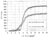
도 2는 결과적으로 얻은 실시예 1-3의 조성물에 대한 콘트라스트 곡선을 보여준다. 종래의 193nm 포토레지스트 조성물을 대표하는 폴리머 A를 포함하는 비교 실시예 1은 NTD 이후 약 40%의 심각한 두께 손실을 보여주는 것으로 입증되었다. 대조적으로, 실시예 2 및 3은 NTD 이후 약 10%의 두께 손실만을 나타내는 것으로 입증되었다. 따라서, 폴리머 A의 MAMA 모노머를 IPGFMA 모노머로 교체하는 것 또는 폴리머 B 또는 C에서처럼 IPGPMA 모노머로 교체하는 것은 NTD 이후 두께 유지 성질을 의미있게 개선시켰다.2 shows the contrast curve for the resulting composition of Examples 1-3. Comparative Example 1, including Polymer A representing a conventional 193 nm photoresist composition, has been shown to show a significant thickness loss of about 40% after NTD. In contrast, Examples 2 and 3 proved to show only about 10% thickness loss after NTD. Thus, replacing the MAMA monomer of Polymer A with IPGFMA monomer or with IPGPMA monomer as in Polymer B or C significantly improved the thickness retention properties after NTD.
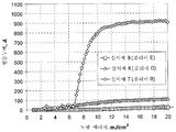
도 3은 실시예 2의 레지스트 조성물 대해 얻은 NTD 콘트라스트 곡선을 각각 폴리머 B 및 D를 사용한 비교 실시예 4와 비교하였다. 폴리머 D(IPGFMA 호모폴리머)를 사용한 비교 실시예 4의 조성물은 약 90%의 두께 손실을 일으키는 수용할 수없는 NTD 콘트라스트를 제공했다. 그러나, 실시예 2에서처럼 락톤을 포함하는 메타크릴 모노머를 갖는 IPGFMA의 코폴리머를 사용하는 경우, 훌륭한 NTD 콘트라스트가 얻어졌다. 비교 실시예 5에서 IPGPMA 호모폴리머("폴리머 E")도 동일하게 관찰되었다. 실시예 3 및 비교 실시예 5에 대한 NTD 콘트라스트 곡선을 제공하는 도 4에서 나타낸 것처럼, 비교 실시예는 약 98%의 두께 손실을 갖는 좋지 못한 NTD 콘트라스트를 제공했다. 실시예 3의 폴리머 C에서 처럼, IPGPMA가 락톤을 포함하는 메타크릴 모노머와 코폴리머화되는 경우, 훌륭한 NTD 콘트라스트가 얻어졌다. 이러한 결과에 기초로 해서, IPGFPMA 또는 IPGPMA를 포함하는 코폴리머 및 락톤을 포함하는 메타크릴 모노머가 각각의 IPGFPMA 또는 IPGPMA 호모폴리머와 비교해서 의미있게 개선된 NTD 콘트라스트를 보여주었다.FIG. 3 compares the NTD contrast curves obtained for the resist composition of Example 2 with Comparative Example 4 using polymers B and D, respectively. The composition of Comparative Example 4 using Polymer D (IPGFMA homopolymer) provided unacceptable NTD contrast resulting in a thickness loss of about 90%. However, when using a copolymer of IPGFMA having a methacryl monomer comprising lactone as in Example 2, excellent NTD contrast was obtained. In Comparative Example 5 the IPGPMA homopolymer (“polymer E”) was also observed. As shown in FIG. 4, which provides NTD contrast curves for Example 3 and Comparative Example 5, Comparative Example provided poor NTD contrast with a thickness loss of about 98%. As in Polymer C of Example 3, good NTD contrast was obtained when IPGPMA was copolymerized with methacryl monomers containing lactones. Based on these results, copolymers containing IPGFPMA or IPGPMA and methacryl monomers containing lactones showed significantly improved NTD contrast compared to respective IPGFPMA or IPGPMA homopolymers.
도 5, 6 및 표 2에서 나타낸 것처럼, 각각의 실시예 1, 2, 4, 및 5와 비교할 때 표면 활성 폴리머(첨가제 A)를 사용하지 않고 제제화된 실시예 6 내지 9의 포토레지스트 조성물의 NTD 콘트라스트에 대해서도 유사한 결과를 얻었다. 따라서, 표면 활성 폴리머의 존재가 제조된 발명의 매트릭스 폴리머의 콘트라스트에 불리한 영향을 끼치지는 않을 것이다.
5, 6 and Table 2, NTD of the photoresist compositions of Examples 6-9 formulated without the use of surface active polymers (Additive A) as compared to Examples 1, 2, 4, and 5, respectively. Similar results were obtained for contrast. Thus, the presence of the surface active polymer will not adversely affect the contrast of the inventive matrix polymer.
패턴 붕괴 평가를 위한 침지 리소그래피 방법Immersion Lithography Method for Evaluating Pattern Collapse
300mm의 실리콘 웨이퍼를 ARTM40A 반사-반사방지제(Rohm and Haas Electronic Materials)로 스핀-코팅하여 텔 클린 트랙 리트머스(TEL CLEAN TRAC LITHIUS) i+ 코터/디벨로퍼 상에 제1 바닥 반사방지 코팅(BARC)을 형성하였다. 웨이퍼를 215 ℃에서 60 초동안 베이킹하여 840 Å의 제1 BARC 필름 두께를 얻었다. 제2 BARC층을 제1 BARC 위에 ARTM124 반사방지제(Rohm and Haas Electronic Materials)를 사용하여 후속 코팅하고, 205 ℃에서 60초동안 베이킹하여 200 Å 탑 BARC 층을 생성하였다. 실시예 1 내지 3의 포토레지스트 제제를 이중 BARC-코팅 웨이퍼에 코팅하고, 100 ℃에서 60 초동안 텔 클린 트랙 리트머스 i+ 코터/디벨로퍼 상에 소프트 베이킹하여 1000 Å의 레지스트 층 두께를 제공하였다.A silicon wafer of 300mm AR TM 40A reflection-spin a reflection preventing agent (Rohm and Haas Electronic Materials) - coated Tel Clean Track litmus (TEL CLEAN TRAC LITHIUS) A first bottom antireflective coating (BARC) was formed on the i + coater / developer. The wafer was baked at 215 ° C. for 60 seconds to obtain a first BARC film thickness of 840 mm 3. The second BARC layer was subsequently coated onto the first BARC using AR ™ 124 antireflective agent (Rohm and Haas Electronic Materials) and baked at 205 ° C. for 60 seconds to produce a 200 kPa top BARC layer. The photoresist formulations of Examples 1-3 were coated on a double BARC-coated wafer and soft baked on a Tel Clean Track litmus i + coater / developer at 100 ° C. for 60 seconds to provide a resist layer thickness of 1000 kPa.
포토레지스트-코팅 웨이퍼를 마스크를 통해서 ASML TWINSCAN XT:1900i 침지 스캐너에서 최대 NA가 1.35인 침지 스캐너를 사용하여 노광하였다. 2개 노광 조건을 각각의 레지스트 조성물에 사용하였다. 단일 노광 NTD 방법에서, C-Quad 20 조사는 1.35 NA, 0.988 외부 시그마, 0.9 내부 시그마 및 XY 편광으로 사용되었다. 인쇄 접촉홀 이미지에 대해 수직 방향의 라인/스페이스 패턴의 이중 노광과 연관되어 있는 이중 노광 NTD 방법에서, 제1 노광은 1.35 NA, 0.97 외부 시그마, 0.82 내부 시그마 및 X 편광을 가지는 쌍극자 조사를 사용하여 실시하였다. 제1 노광 단계 직후에, 웨이퍼를 제1 마스크의 라인에 수직인 라인을 가지는 상이한 마스크로 1.35 NA, 0.97 외부 시그마, 0.82 내부 시그마 및 Y 편광을 가지는 쌍극자 조사를 사용하여 다시 노광하였다. 노광된 웨이퍼를 100 내지 120 ℃에서 60 초동안 노광 후 베이킹한 다음, 2-헵타논을 사용하여 25 초동안 텔 클린 트랙 리트머스 i+ 코터/디벨로퍼 상에서 현상하여 네가티브 톤 패턴을 얻었다. 임계 크기(CD)를 히타치(Hitachi) CG4000 CD SEM에서 다양한 마스크 CD 및 피치로 측정하여 패턴을 패턴 붕괴 발생에 대하여 검사하였다.The photoresist-coated wafer was exposed through a mask using an immersion scanner with a maximum NA of 1.35 in an ASML TWINSCAN XT: 1900i immersion scanner. Two exposure conditions were used for each resist composition. In the single exposure NTD method, C-
폴리머 B 및 C를 사용하는 실시예 2와 3의 조성물은 각각 폴리머 A를 사용하는 비교 실시예 1의 조성물과 비교하여 훨씬 우수한 패턴 붕괴 마진을 나타내었다. 도 7A-C는 32mJ/cm2에서 실시예 1 내지 3의 조성물 각각에 대해 80nm 피치에서 40nm 라인의 마스크 CD로 얻어진 CD의 SEM 현미경사진 이미지를 나타낸 것이다. 쌍극자 조사 조건은 1.35 NA, 0.97 외부 시그마, 0.82 내부 시그마 및 X 편광을 사용하였다. 비교예 1은 심각한 패턴 붕괴를 나타내는 것이 확인되었고, 실시예 2와 3은 훌륭한 붕괴 마진을 제공하는 것으로 확인되었다.The compositions of Examples 2 and 3 using Polymers B and C showed much better pattern collapse margins compared to the compositions of Comparative Example 1 using Polymer A, respectively. 7A-C show SEM micrograph images of CDs obtained with mask CDs of 40 nm lines at 80 nm pitch for each of the compositions of Examples 1-3 at 32 mJ / cm 2 . Dipole irradiation conditions used 1.35 NA, 0.97 outer sigma, 0.82 inner sigma and X polarization. It was confirmed that Comparative Example 1 exhibited severe pattern collapse, and Examples 2 and 3 provided excellent collapse margins.
Claims (10)
포토애시드 발생제(photoacid generator)
를 포함하는 포토레지스트 조성물:


상기 식에서,
R1 및 R2는 독립적으로 (C1-C10) 선형, 분지형 및 환형 유기 기로부터 선택되거나, 또는 함께, 임의로 환을 형성하며;
a 또는 b중 하나는 1이고, a 또는 b중 다른 하나는 1 또는 2이며;
R3 및 R4는 독립적으로 (C1-C10) 선형, 분지형 및 환형 유기 기로부터 선택되거나, 또는 함께, 임의로 환을 형성하며;
c 또는 d중 하나는 1이고, c 또는 d중 다른 하나는 1 또는 2이다.A first unit formed from a monomer comprising a polymerizable functional group and a first portion of formula (I) or formula (II) below; And copolymers that contain one or more additional units and that do not contain acid cutters that can form carboxylic acid groups by cleavage; And
Photoacid generator
Photoresist composition comprising:
Where
R 1 and R 2 is independently selected from (C 1 -C 10 ) linear, branched and cyclic organic groups, or together, optionally forms a ring;
one of a or b is 1 and the other of a or b is 1 or 2;
R 3 and R 4 is independently selected from (C 1 -C 10 ) linear, branched and cyclic organic groups, or together, optionally forms a ring;
one of c or d is 1 and the other of c or d is 1 or 2.
(b) 상기 패턴화될 하나 이상의 층 위에 제 1 항 내지 8 항중 어느 한 항의 포토레지스트 조성물층을 도포하는 단계;
(c) 상기 포토레지스트 조성물층을 화학 조사선에 패턴식으로 노광시키는 단계;
(d) 상기 노광된 포토레지스트 조성물 층을 노광후 베이킹(post-exposure bake) 공정에서 가열하는 단계; 및
(e) 상기 포토레지스트 조성물 층에 현상제를 적용하는 단계(여기서 포토레지스트 층의 비노광 영역은 현상제에 의해 제거되고, 포토레지스트 층의 노광 영역은 패턴화될 하나 이상의 층 위에 포토레지스트 패턴을 형성한다)
를 포함하는, 포토리소그래피 패턴의 형성 방법.
(a) providing a substrate comprising one or more layers to be patterned on the substrate surface;
(b) applying the photoresist composition layer of claim 1 on at least one layer to be patterned;
(c) patternwise exposing the photoresist composition layer to actinic radiation;
(d) heating the exposed photoresist composition layer in a post-exposure bake process; And
(e) applying a developer to the photoresist composition layer, wherein the non-exposed areas of the photoresist layer are removed by the developer, and the exposed areas of the photoresist layer apply a photoresist pattern over one or more layers to be patterned. Forms)
Comprising a photolithography pattern.
Applications Claiming Priority (2)
| Application Number | Priority Date | Filing Date | Title |
|---|---|---|---|
| US38180510P | 2010-09-10 | 2010-09-10 | |
| US61/381,805 | 2010-09-10 |
Publications (1)
| Publication Number | Publication Date |
|---|---|
| KR20120026991A true KR20120026991A (en) | 2012-03-20 |
Family
ID=44785344
Family Applications (1)
| Application Number | Title | Priority Date | Filing Date |
|---|---|---|---|
| KR1020110091582A KR20120026991A (en) | 2010-09-10 | 2011-09-09 | Photoresist compositions and methods of forming photolithographic patterns |
Country Status (7)
| Country | Link |
|---|---|
| US (1) | US20120064456A1 (en) |
| EP (2) | EP2428843A1 (en) |
| JP (2) | JP2012103679A (en) |
| KR (1) | KR20120026991A (en) |
| CN (1) | CN102445848B (en) |
| IL (1) | IL215078A0 (en) |
| TW (1) | TWI556059B (en) |
Cited By (1)
| Publication number | Priority date | Publication date | Assignee | Title |
|---|---|---|---|---|
| KR20150075025A (en) | 2013-12-24 | 2015-07-02 | 금호석유화학 주식회사 | Novel monomer, polymer and resist composition comprising the same |
Families Citing this family (13)
| Publication number | Priority date | Publication date | Assignee | Title |
|---|---|---|---|---|
| JP5767919B2 (en) * | 2010-09-17 | 2015-08-26 | 富士フイルム株式会社 | Pattern formation method |
| JP5947028B2 (en) * | 2010-12-02 | 2016-07-06 | ローム アンド ハース エレクトロニック マテリアルズ エルエルシーRohm and Haas Electronic Materials LLC | Polymer, photoresist composition, and method for forming a photolithography pattern |
| EP2472325A1 (en) * | 2010-12-31 | 2012-07-04 | Rohm and Haas Electronic Materials LLC | Polymers, photoresist compositions and methods of forming photolithographic patterns |
| JP6118500B2 (en) * | 2011-02-28 | 2017-04-19 | ローム アンド ハース エレクトロニック マテリアルズ エルエルシーRohm and Haas Electronic Materials LLC | Photoresist composition and method for forming photolithography pattern |
| JP2015180950A (en) * | 2012-01-31 | 2015-10-15 | 富士フイルム株式会社 | Actinic ray-sensitive or radiation-sensitive resin composition, and resist film, pattern forming method, manufacturing method of electronic device and electronic device which use the composition |
| JP2014101438A (en) * | 2012-11-19 | 2014-06-05 | Fujifilm Corp | Acetal compound and acetal polymer compound |
| US9057960B2 (en) * | 2013-02-04 | 2015-06-16 | International Business Machines Corporation | Resist performance for the negative tone develop organic development process |
| TWI584061B (en) * | 2014-08-27 | 2017-05-21 | 羅門哈斯電子材料有限公司 | Multiple-pattern forming methods |
| CN106094431B (en) | 2015-04-30 | 2020-06-26 | 罗门哈斯电子材料韩国有限公司 | Photoresist composition and method |
| US11480878B2 (en) | 2016-08-31 | 2022-10-25 | Rohm And Haas Electronic Materials Korea Ltd. | Monomers, polymers and photoresist compositions |
| CN108264605A (en) | 2016-12-30 | 2018-07-10 | 罗门哈斯电子材料韩国有限公司 | Monomer, polymer and photo-corrosion-resisting agent composition |
| JP6730417B2 (en) | 2017-12-31 | 2020-07-29 | ローム アンド ハース エレクトロニック マテリアルズ エルエルシーRohm and Haas Electronic Materials LLC | Photoresist composition and method |
| US11874603B2 (en) | 2021-09-15 | 2024-01-16 | Rohm And Haas Electronic Materials Korea Ltd. | Photoresist composition comprising amide compound and pattern formation methods using the same |
Family Cites Families (33)
| Publication number | Priority date | Publication date | Assignee | Title |
|---|---|---|---|---|
| JPH0250126A (en) * | 1988-08-12 | 1990-02-20 | Asahi Glass Co Ltd | Image display device |
| JPH0950126A (en) * | 1995-08-08 | 1997-02-18 | Fujitsu Ltd | Resist composition and resist pattern forming method |
| WO1997033198A1 (en) | 1996-03-07 | 1997-09-12 | The B.F. Goodrich Company | Photoresist compositions comprising polycyclic polymers with acid labile pendant groups |
| US5856150A (en) * | 1996-10-18 | 1999-01-05 | Amerchol Corporation | Selective hydrolysis of saturated esters over unsaturated esters using enzymes |
| KR100273172B1 (en) * | 1998-08-01 | 2001-03-02 | 윤덕용 | Photoresist using a compound having a dioxaspirocyclic derivative in the acrylic side chain |
| WO2001025853A1 (en) * | 1999-10-07 | 2001-04-12 | Clariant International Ltd. | Photosensitive composition |
| KR100749494B1 (en) * | 2001-04-03 | 2007-08-14 | 삼성에스디아이 주식회사 | Polymer for chemical amplification negative photoresist and photoresist composition |
| KR20020077948A (en) * | 2001-04-03 | 2002-10-18 | 삼성에스디아이 주식회사 | Monomer for photoresist, polymer for photoresist, photoresist composition and phosphor composition for color cathode ray tube |
| US7214465B2 (en) * | 2002-01-10 | 2007-05-08 | Fujifilm Corporation | Positive photosensitive composition |
| KR20050063234A (en) * | 2003-12-22 | 2005-06-28 | 주식회사 하이닉스반도체 | Photoresist polymer and photoresist composition containing it |
| KR20060066932A (en) * | 2004-12-14 | 2006-06-19 | 주식회사 하이닉스반도체 | Photoresist polymer and photoresist composition containing the same |
| EP1684120A1 (en) * | 2005-01-19 | 2006-07-26 | Rohm and Haas Electronic Materials LLC | Photresist compositions comprising resin blends |
| JP4796792B2 (en) * | 2005-06-28 | 2011-10-19 | 富士フイルム株式会社 | Positive photosensitive composition and pattern forming method using the same |
| JP5111895B2 (en) * | 2006-03-10 | 2013-01-09 | ローム・アンド・ハース・エレクトロニック・マテリアルズ,エル.エル.シー. | Photolithographic compositions and methods |
| JP2008159874A (en) * | 2006-12-25 | 2008-07-10 | Tokyo Ohka Kogyo Co Ltd | Method for forming resist pattern |
| US8530148B2 (en) * | 2006-12-25 | 2013-09-10 | Fujifilm Corporation | Pattern forming method, resist composition for multiple development used in the pattern forming method, developer for negative development used in the pattern forming method, and rinsing solution for negative development used in the pattern forming method |
| JP2008233877A (en) * | 2007-02-23 | 2008-10-02 | Fujifilm Corp | Negative resist composition and pattern forming method using the same |
| JP4617337B2 (en) * | 2007-06-12 | 2011-01-26 | 富士フイルム株式会社 | Pattern formation method |
| JP5002360B2 (en) * | 2007-07-23 | 2012-08-15 | 富士フイルム株式会社 | Pattern formation method |
| JP2009063889A (en) * | 2007-09-07 | 2009-03-26 | Fujifilm Corp | Positive photosensitive composition, polymerizable compound, resin and pattern forming method |
| JP5449675B2 (en) * | 2007-09-21 | 2014-03-19 | 富士フイルム株式会社 | Photosensitive composition, pattern forming method using the photosensitive composition, and compound used in the photosensitive composition |
| KR20090059650A (en) * | 2007-12-07 | 2009-06-11 | 삼성전자주식회사 | Photoresist composition for an immersion lithography and method of forming a photoresist pattern using the same |
| WO2009113459A1 (en) * | 2008-03-10 | 2009-09-17 | 旭化成イーマテリアルズ株式会社 | Photosensitive polyorganosiloxane composition |
| US9046773B2 (en) * | 2008-03-26 | 2015-06-02 | Fujifilm Corporation | Actinic ray-sensitive or radiation-sensitive resin composition, pattern forming method using the same, polymerizable compound and polymer compound obtained by polymerizing the polymerizable compound |
| JP5433181B2 (en) * | 2008-03-28 | 2014-03-05 | 富士フイルム株式会社 | Negative resist composition for development and pattern forming method using the same |
| TWI462938B (en) * | 2008-05-21 | 2014-12-01 | Sumitomo Chemical Co | Polymer and chemically amplified resist composition comprising the same |
| JP5639755B2 (en) * | 2008-11-27 | 2014-12-10 | 富士フイルム株式会社 | Pattern forming method using developer containing organic solvent and rinsing solution used therefor |
| JP5371805B2 (en) * | 2010-01-25 | 2013-12-18 | 富士フイルム株式会社 | Actinic ray-sensitive or radiation-sensitive resin composition and pattern forming method using the same |
| JP5775701B2 (en) * | 2010-02-26 | 2015-09-09 | 富士フイルム株式会社 | Pattern forming method and resist composition |
| JP5647804B2 (en) * | 2010-03-19 | 2015-01-07 | 富士フイルム株式会社 | Resist composition and pattern forming method using the same |
| JP5708082B2 (en) * | 2010-03-24 | 2015-04-30 | 信越化学工業株式会社 | Pattern forming method and negative resist composition |
| JP5802369B2 (en) * | 2010-07-29 | 2015-10-28 | 富士フイルム株式会社 | Actinic ray-sensitive or radiation-sensitive resin composition, and resist film and pattern forming method using the same |
| JP2013097272A (en) * | 2011-11-02 | 2013-05-20 | Tokyo Ohka Kogyo Co Ltd | Resist composition and method for forming resist pattern |
-
2011
- 2011-09-08 JP JP2011195533A patent/JP2012103679A/en active Pending
- 2011-09-08 EP EP11180515A patent/EP2428843A1/en not_active Withdrawn
- 2011-09-08 EP EP12180298A patent/EP2527919A1/en not_active Withdrawn
- 2011-09-09 KR KR1020110091582A patent/KR20120026991A/en not_active Application Discontinuation
- 2011-09-10 US US13/229,672 patent/US20120064456A1/en not_active Abandoned
- 2011-09-11 IL IL215078A patent/IL215078A0/en unknown
- 2011-09-13 CN CN201110430673.7A patent/CN102445848B/en not_active Expired - Fee Related
- 2011-09-13 TW TW100132797A patent/TWI556059B/en not_active IP Right Cessation
-
2016
- 2016-03-07 JP JP2016043392A patent/JP2016148856A/en active Pending
Cited By (1)
| Publication number | Priority date | Publication date | Assignee | Title |
|---|---|---|---|---|
| KR20150075025A (en) | 2013-12-24 | 2015-07-02 | 금호석유화학 주식회사 | Novel monomer, polymer and resist composition comprising the same |
Also Published As
| Publication number | Publication date |
|---|---|
| IL215078A0 (en) | 2012-02-29 |
| US20120064456A1 (en) | 2012-03-15 |
| EP2428843A1 (en) | 2012-03-14 |
| TWI556059B (en) | 2016-11-01 |
| CN102445848A (en) | 2012-05-09 |
| TW201217907A (en) | 2012-05-01 |
| JP2016148856A (en) | 2016-08-18 |
| EP2527919A1 (en) | 2012-11-28 |
| JP2012103679A (en) | 2012-05-31 |
| CN102445848B (en) | 2015-08-05 |
Similar Documents
| Publication | Publication Date | Title |
|---|---|---|
| KR102064809B1 (en) | Photoresist compositions and methods of forming photolithographic patterns | |
| US8790867B2 (en) | Methods of forming photolithographic patterns by negative tone development | |
| KR101854145B1 (en) | Photoresist compositions and methods of forming photolithographic patterns | |
| TWI556059B (en) | Photoresist compositions and methods of forming photolithographic patterns | |
| JP6080357B2 (en) | Polymer, photoresist composition, and method for forming a photolithography pattern | |
| KR101838960B1 (en) | Polymers, photoresist compositions and methods of forming photolithographic patterns | |
| KR101910832B1 (en) | Photoresist compositions and methods of forming photolithographic patterns | |
| KR20120078673A (en) | Monomers, photoresist compositions and methods of forming photolithographic patterns | |
| JP6130099B2 (en) | Polymer, photoresist composition, and method for forming a photolithography pattern | |
| JP2017125200A (en) | Monomers, polymers and photoresist compositions |
Legal Events
| Date | Code | Title | Description |
|---|---|---|---|
| N231 | Notification of change of applicant | ||
| A201 | Request for examination | ||
| E902 | Notification of reason for refusal | ||
| E601 | Decision to refuse application |