KR20120002402A - Current conductor for a galvanic cell - Google Patents
Current conductor for a galvanic cell Download PDFInfo
- Publication number
- KR20120002402A KR20120002402A KR1020107013141A KR20107013141A KR20120002402A KR 20120002402 A KR20120002402 A KR 20120002402A KR 1020107013141 A KR1020107013141 A KR 1020107013141A KR 20107013141 A KR20107013141 A KR 20107013141A KR 20120002402 A KR20120002402 A KR 20120002402A
- Authority
- KR
- South Korea
- Prior art keywords
- conductor
- region
- sealing
- galvanic cell
- package
- Prior art date
Links
Images


Classifications
-
- H—ELECTRICITY
- H01—ELECTRIC ELEMENTS
- H01M—PROCESSES OR MEANS, e.g. BATTERIES, FOR THE DIRECT CONVERSION OF CHEMICAL ENERGY INTO ELECTRICAL ENERGY
- H01M4/00—Electrodes
- H01M4/02—Electrodes composed of, or comprising, active material
- H01M4/64—Carriers or collectors
- H01M4/70—Carriers or collectors characterised by shape or form
-
- H—ELECTRICITY
- H01—ELECTRIC ELEMENTS
- H01M—PROCESSES OR MEANS, e.g. BATTERIES, FOR THE DIRECT CONVERSION OF CHEMICAL ENERGY INTO ELECTRICAL ENERGY
- H01M50/00—Constructional details or processes of manufacture of the non-active parts of electrochemical cells other than fuel cells, e.g. hybrid cells
- H01M50/50—Current conducting connections for cells or batteries
-
- H—ELECTRICITY
- H01—ELECTRIC ELEMENTS
- H01M—PROCESSES OR MEANS, e.g. BATTERIES, FOR THE DIRECT CONVERSION OF CHEMICAL ENERGY INTO ELECTRICAL ENERGY
- H01M10/00—Secondary cells; Manufacture thereof
- H01M10/05—Accumulators with non-aqueous electrolyte
- H01M10/052—Li-accumulators
- H01M10/0525—Rocking-chair batteries, i.e. batteries with lithium insertion or intercalation in both electrodes; Lithium-ion batteries
-
- H—ELECTRICITY
- H01—ELECTRIC ELEMENTS
- H01M—PROCESSES OR MEANS, e.g. BATTERIES, FOR THE DIRECT CONVERSION OF CHEMICAL ENERGY INTO ELECTRICAL ENERGY
- H01M50/00—Constructional details or processes of manufacture of the non-active parts of electrochemical cells other than fuel cells, e.g. hybrid cells
- H01M50/50—Current conducting connections for cells or batteries
- H01M50/531—Electrode connections inside a battery casing
- H01M50/54—Connection of several leads or tabs of plate-like electrode stacks, e.g. electrode pole straps or bridges
-
- H—ELECTRICITY
- H01—ELECTRIC ELEMENTS
- H01M—PROCESSES OR MEANS, e.g. BATTERIES, FOR THE DIRECT CONVERSION OF CHEMICAL ENERGY INTO ELECTRICAL ENERGY
- H01M50/00—Constructional details or processes of manufacture of the non-active parts of electrochemical cells other than fuel cells, e.g. hybrid cells
- H01M50/50—Current conducting connections for cells or batteries
- H01M50/543—Terminals
-
- Y—GENERAL TAGGING OF NEW TECHNOLOGICAL DEVELOPMENTS; GENERAL TAGGING OF CROSS-SECTIONAL TECHNOLOGIES SPANNING OVER SEVERAL SECTIONS OF THE IPC; TECHNICAL SUBJECTS COVERED BY FORMER USPC CROSS-REFERENCE ART COLLECTIONS [XRACs] AND DIGESTS
- Y02—TECHNOLOGIES OR APPLICATIONS FOR MITIGATION OR ADAPTATION AGAINST CLIMATE CHANGE
- Y02E—REDUCTION OF GREENHOUSE GAS [GHG] EMISSIONS, RELATED TO ENERGY GENERATION, TRANSMISSION OR DISTRIBUTION
- Y02E60/00—Enabling technologies; Technologies with a potential or indirect contribution to GHG emissions mitigation
- Y02E60/10—Energy storage using batteries
Landscapes
- Chemical & Material Sciences (AREA)
- Chemical Kinetics & Catalysis (AREA)
- Electrochemistry (AREA)
- General Chemical & Material Sciences (AREA)
- Engineering & Computer Science (AREA)
- Materials Engineering (AREA)
- Manufacturing & Machinery (AREA)
- Connection Of Batteries Or Terminals (AREA)
- Sealing Battery Cases Or Jackets (AREA)
- Secondary Cells (AREA)
Abstract
본 발명은 서로 마주하고 제1 측면(18) 및 제2 측면(19)에 의해 서로 연결된 제1 표면(16) 및 제2 표면(17)을 포함하는 갈바니 전지용 판상의 전도체를 제공한다. 상기 갈바니 전지용 전도체의 밀봉 성능을 향상시키기 위해, 상기 제1 및/또는 제2 측면(18,19)의 영역 내에서, 상기 제1 및 제2 표면(16, 17)에 의하여 정의된 상기 전도체의 두께와 비교할 때 감소된 단면 두께를 갖고, 적어도 상기 전도체의 밀봉 영역(14)에 걸쳐 연장되는 부분을 포함한다.The present invention provides a plate-shaped conductor for galvanic cells comprising a first surface 16 and a second surface 17 facing each other and connected to each other by a first side 18 and a second side 19. In order to improve the sealing performance of the conductor for galvanic cells, within the region of the first and / or second side surfaces 18, 19, of the conductor defined by the first and second surfaces 16, 17. It has a reduced cross-sectional thickness as compared to the thickness and includes at least a portion extending over the sealing region 14 of the conductor.
Description
본 발명은 갈바니 전지용 전도체 및 이를 포함하는 갈바니 전지에 관한 것이다.The present invention relates to a galvanic cell conductor and a galvanic cell comprising the same.
리튬 이온 전지와 같은 갈바니 전지는 대부분의 경우에 있어서 교대로 적층된 다수의 전극과 세퍼레이터를 포함하여 구성되고, 상기 각 전극에는 전도체(current conductor)가 형성 또는 부착되어 있다. 이러한 더미(stack)는 일반적으로 패키지 내에 수납되어 있고, 전도체는 패키지로부터 돌출되어 있다. 이 경우 상기 전도체들의 돌출부위는 패키지에 의해 밀봉된다. 이러한 전지 몇개가 예컨대 리튬 이온 축전지 내에 포함될 수 있다.A galvanic cell, such as a lithium ion cell, in most cases comprises a plurality of electrodes and separators that are alternately stacked, and each electrode has a current conductor formed or attached thereto. Such a stack is generally housed in a package and the conductor protrudes from the package. In this case, the protrusion of the conductors is sealed by the package. Several such cells can be included, for example, in lithium ion accumulators.
최근에, 리튬 이온 전지는 전기 자동차 및 하이브리드 전기 자동차에서 증가적으로 사용되고 있다. 이러한 적용에 있어서는 충전 및 방전 과정에서 매우 높은 전류가 전극과 연결되어 있는 전류 컬렉터(current collector)를 통해서 흐르게 된다. 대략 200 암페어의 항류(permanent current)를 기준으로 전류 컬렉터의 온도는 예를 들어 5O℃를 넘으면 안되는데, 그 이유는 온도 상승이 에너지 손실을 초래함과 더불어 리튬 이온 전지의 신뢰성을 저하시키기 때문이다.Recently, lithium ion batteries have been increasingly used in electric vehicles and hybrid electric vehicles. In this application, a very high current flows through a current collector connected to the electrode during charging and discharging. The temperature of the current collector should not exceed 50 ° C., for example based on a permanent current of approximately 200 amperes, because the rise in temperature results in energy loss and reduces the reliability of the lithium ion battery.
에너지의 열 전환을 감소시키기 위하여 예컨대 전도체의 단면을 확대할 수 있다. 그러나, 리튬 이온 전지의 면적은 제한된 설치 공간으로 인하여 미리 정해져 있거나 한정되어 있기 때문에, 전도체는 일정 크기 이상 더 넓게 만들 수 없다. 따라서 많은 경우에 있어서는 두꺼운 전류 컬렉터를 사용할 필요가 있다.
To reduce the thermal conversion of energy, for example, the cross section of the conductor can be enlarged. However, since the area of a lithium ion battery is predetermined or limited due to limited installation space, the conductor cannot be made wider than a certain size. Therefore, in many cases it is necessary to use thick current collectors.
본 발명은 그 두께와 관계없이 안전하고 내구성 있는 밀봉(sealing)이 보장되는 갈바니 전지를 위한 전도체를 제공함에 목적이 있다.
It is an object of the present invention to provide a conductor for a galvanic cell in which a safe and durable sealing is ensured regardless of its thickness.
상기한 과제는 청구항 1의 특징을 갖는 갈바니 전지용 판상(plate-shaped) 전도체를 통하여 해결된다. 본 발명의 진보된 실시예들과 개선들은 종속항의 주제이다.The above problem is solved through a plate-shaped conductor for a galvanic battery having the features of claim 1. Advanced embodiments and improvements of the invention are the subject of the dependent claims.
갈바니 전지를 위한 판상 전도체는 서로 마주하는 제1 표면과 제2 표면을 포함함과 더불어 제1 측면 및 제2 측면을 통하여 서로 연결된다.The plate conductors for galvanic cells are connected to each other through first and second sides as well as including first and second surfaces facing each other.
본 발명에 따르면, 판상의 전도체는 제1 및/또는 제2 측면의 영역 내에서 전도체의 제1 및 제2 표면에 의하여 정의되는 두께에 비하여 축소된 두께를 갖는 부분을 구비하고, 이 부분은 적어도 전도체의 밀봉 영역 이상으로 연장된다.According to the invention, the plate-shaped conductor has a portion in the region of the first and / or second side having a reduced thickness compared to the thickness defined by the first and second surfaces of the conductor, the portion having at least Extend beyond the sealing area of the conductor.
단면에 있어서 상기 전도체에서 적어도 하나의 측면 영역 내에서 감소된 두께를 가진 부분의 형성에 의해 더 두꺼운 전도체의 경우에서도 문제없이 그리고 결함 유발 없이 상기 전도체 및 적절한 패키지 사이의 안전하고 안정적인 밀봉이 이루어질 수 있으며, 이에 따라 상기 갈바니 전지의 신뢰할 수 있고 지속적인 밀봉이 가능해진다.The formation of a portion with reduced thickness in the at least one side region in the conductor in cross section allows a safe and stable sealing between the conductor and the appropriate package without problems and even in the case of thicker conductors, Thus, reliable and lasting sealing of the galvanic cell is possible.
본 발명에서, 갈바니 전지란 배터리용 전지 내지 1차 배터리 그리고 특히 재충전 가능한 배터리 내지 2차 배터리 또는 축전지를 가리킨다. 상기 전도체는 충전 전류를 상기 전극으로 유도하기 위하여 또는 방전 전류를 상기 전극에서 방전하기 위하여, 일반적으로 상기 갈바니 전지의 전극(애노드 또는 캐소드)과 연결이 되어 있거나 또는 일체로 형성된 부재이며, 전기 전도성 재료로 형성된 부재이다.In the present invention, a galvanic cell refers to a battery for a battery or a primary battery and in particular a rechargeable battery or a secondary battery or a storage battery. The conductor is generally a member connected to or integrally formed with an electrode (anode or cathode) of the galvanic cell to induce a charge current to the electrode or to discharge a discharge current from the electrode. It is a member formed by.
상기 전도체는 서로 마주하는 제1 표면 및 제2 표면을 포함하는 판상의 몸체이며, 예를 들어 직육면체 형태의 전도체의 경우, 상기 몸체의 가장 큰 양면을 형성하며, 이것은 통상적으로 해당 전극의 주 확장면에 대하여 평행하게 정렬되어 있다. 상기 제1 측면 및 상기 제2 측면은 기본적으로 서로 마주하고 있으며 상기 전도체의 제1 표면 및 제2 표면을 연결한다. 직육면체 형태의 전도체의 경우 남아 있는 두 개의 측면은 본 발명에 있어서 의미가 없다.The conductor is a plate-like body comprising a first surface and a second surface facing each other, for example in the case of a cuboid-shaped conductor, it forms the largest two sides of the body, which is typically the main expanding surface of the electrode. It is aligned parallel to. The first side and the second side are basically opposite to each other and connect the first and second surfaces of the conductor. In the case of a cuboid conductor, the remaining two aspects are meaningless in the present invention.
상기 판상의 전도체의 상기 제1 표면 및 상기 제2 표면에 의하여 상기 전도체의 두께(D)가 정의된다. 기본적으로 평행의 측면인 경우, 이와 같은 두께(D)는 기본적으로 상기 양 측면 영역 사이에서의 상기 전도체의 일정한 두께이다. 평행하진 않는 측면인 경우, 상기 전도체의 두께(D)는 상기 양 측면 영역 사이에서의 최대 두께, 또는 상기 양 측면 영역 사이에서의 평균 두께가 될 수 있다. 단면에 있어서 감소된 두께를 갖는 부분은 상기 전도체의 두께(D)에 비해서 상기 제1 및 제2 측면 내에서의 감소된 두께(d)를 가지며, 이는 예를 들어서 상기 전도체 몸체의 전체 영역에 거쳐서 최소 두께가 될 수 있다. 측면 영역 내에서, 일반적으로 하나 또는 그 이상의 감소된 두께를 갖는 그러한 부분이 제공될 수 있으며, 이는 동일한 또는 서로 다른 두께를 갖는다.The thickness D of the conductor is defined by the first surface and the second surface of the plate-like conductor. In the case of basically parallel sides, this thickness D is basically a constant thickness of the conductor between the two side regions. In the case of non-parallel side surfaces, the thickness D of the conductor may be a maximum thickness between the two side regions, or an average thickness between the two side regions. The part with the reduced thickness in cross section has a reduced thickness d in the first and second side as compared to the thickness D of the conductor, for example over the entire area of the conductor body. It can be the minimum thickness. Within the lateral area, such parts may generally be provided with one or more reduced thicknesses, which have the same or different thicknesses.
상기 밀봉 영역은 상기 전도체의 전체 표면 및 측면을 둘러쌓지 않으며, 일반적으로 하나의 일부 영역만, 즉 그것의 수직 단면만 둘러쌓는다. 갈바니 전지에 있어서 상기 전도체의 밀봉 영역은 해당하는 패키지의 밀봉 영역에 접촉되며, 이는 그 사이에 개재된 밀봉층을 통하여 두 구성 요소 사이의 밀봉을 형성하기 위한 것이다.The sealing region does not surround the entire surface and side of the conductor and generally only one partial region, ie only its vertical cross section. In galvanic cells the sealing region of the conductor is in contact with the sealing region of the corresponding package, to form a seal between the two components via a sealing layer interposed therebetween.
본 발명이 직육면체 형태의 전도체의 실시예를 통하여 아래에서 상세히 설명된다 하더라도, 당 분야의 전문가가 상기 판상의 전도체의 표면을 다른 기하학적 형태(예를 들어서 평행하게 마주하지 않은 측면, 직사각형 형태가 아닌 표면 등)로 상기한 의미로서 정의할 수 있음은 명확하다.Although the present invention is described in detail below through embodiments of a cuboid-shaped conductor, one skilled in the art will appreciate that the surface of the plate-shaped conductor may have different geometrical shapes (e.g. sides that do not face in parallel, non-rectangular surfaces). Etc.) can be defined as the above meaning.
본 발명에 따른 일 실시예에 있어서, 상기 제1 및/또는 제2 측면의 영역 내에서 감소된 두께를 갖는 부분은 기본적으로 상기 제1 또는 제2 측면의 전체 높이에 걸쳐 연장된다. 본 발명에 따른 다른 실시예에 있어서, 상기 제1 및/또는 제2 측면의 영역 내에서 감소된 두께를 갖는 부분은 기본적으로 상기 전도체의 밀봉 영역에 걸쳐 연장된다.In one embodiment according to the invention, the part having a reduced thickness in the region of the first and / or second side extends essentially over the entire height of the first or second side. In another embodiment according to the invention, the part having a reduced thickness in the region of the first and / or second side extends essentially over the sealing region of the conductor.
본 발명에 따른 또 다른 실시예에 있어서, 상기 제1 및/또는 제2 측면의 영역 내에서 감소된 두께를 갖는 부분은, 상기 제1 및 제2 표면으로 병합되는 하나의 표면 부분에 의하여 형성된다. 또 다른 방식으로, 상기 제1 및/또는 제2 측면의 영역 내에서 감소된 두께를 갖는 부분은, 한 편으로는 서로 병합하고 다른 한 편으로는 상기 제1 및 제2 표면에 병합되는 적어도 두 개의 표면 부분에 의해 형성된다.In yet another embodiment according to the invention, the portion with reduced thickness in the region of the first and / or second side is formed by one surface portion incorporated into the first and second surface. . In another way, at least two portions having reduced thickness in the region of the first and / or second side merge on one side with one another and on the other side with the first and second surface. Formed by the surface portions of the dog.
본 발명에 따른 또 다른 실시예에 있어서 상기 제1 및/또는 제2 측면의 영역 내에서 감소된 두께를 갖는 부분의 표면 부분(들)은 기본적으로 평평한 표면으로 형성되어 있다. 또 다른 방식으로, 상기 제1 및/또는 제2 측면의 영역 내에서 감소된 두께를 갖는 부분의 표면 부분(들)은 굴곡진 표면으로서 형성되어 있다. 표면 부분이 복수인 경우, 이들 부분들은 평평한 표면으로 형성된 표면 부분 및 굴곡진 표면으로 형성된 표면 부분을 포함할 수 있다.In another embodiment according to the invention the surface part (s) of the part having the reduced thickness in the region of the first and / or second side is formed essentially of a flat surface. In another way, the surface portion (s) of the portion with reduced thickness in the region of the first and / or second side is formed as a curved surface. When there are a plurality of surface portions, these portions may include surface portions formed of flat surfaces and surface portions formed of curved surfaces.
굴곡진 표면 부분의 경우, 이것들은 선택적으로 오목하게 또는 볼록하게 굴곡져 있을 수 있으며 또는 부분에 따라서 오목하게 또는 볼록하게 형성되어 있을 수 있다.In the case of curved surface portions, they may be selectively concave or convexly curved or may be concave or convex depending on the portion.
본 발명에 따른 또 다른 실시예에 있어서, 상기 제1 및/또는 제2 측면의 영역 내에서 감소된 두께를 갖는 부분의 표면 부분(들)은 제1 또는 제2 표면에 대해 대략 15° 내지 대략 40°, 바람직하게는 대략 20° 내지 대략 30°의 평균 각도로 기울어져 형성되어 있다.In yet another embodiment according to the invention, the surface portion (s) of the portion having a reduced thickness in the region of the first and / or second side is from about 15 ° to about 1 relative to the first or second surface. It is formed at an angle of 40 °, preferably at an average angle of about 20 ° to about 30 °.
그 밖에도 상기 제1 및/또는 제2 측면의 영역 내에서 감소된 두께를 갖는 부분의 표면 부분(들)은 선택적으로 대칭적으로 또는 비대칭적으로 형성될 수 있다.In addition, the surface portion (s) of the portion with reduced thickness in the region of the first and / or second side may be selectively formed symmetrically or asymmetrically.
이와 유사하게, 제1 측면의 영역 및 제2 측면의 영역은 서로 대칭적으로 또는 비대칭적으로 형성될 수 있다Similarly, the region of the first side and the region of the second side may be formed symmetrically or asymmetrically with each other.
본 발명에 따른 또 다른 실시예에 있어서, 상기 표면 부분 및 상기 표면 사이의 중첩 영역 및/또는 몇 개의 표면 부분들 사이의 중첩 영역은 단면상 연속적으로, 다시 말해 모서리가 개재되지 않는 상태로 형성될 수 있다. 또 다른 방식으로, 이 중첩 영역들은 또한 불연속적으로, 다시 말해 모서리가 개재된 상태로 형성될 수 있다.In another embodiment according to the invention, the surface portion and the overlapping region between the surface and / or the overlapping region between several surface portions can be formed continuously in cross section, that is, without interposing corners. have. In another way, these overlapping regions can also be formed discontinuously, ie with the edge interposed.
본 발명에 따른 하나의 실시예에 있어서, 상기 전도체는 밀봉 영역 내에서 하나의 밀봉층을 포함하여 형성된다. 다시 말해, 상기 전도체는 미리 밀봉되어 있다.In one embodiment according to the invention, the conductor is formed comprising one sealing layer in the sealing area. In other words, the conductor is pre-sealed.
이 경우, 상기 밀봉층은 상기 전도체의 상기 제1 및 제2 표면 그리고 상기 제1 및 제2 측면의 주위를 둘러쌓고 있다. 상기 밀봉층은, 바람직하게는, 예를 들어 폴리에틸렌, 폴리프로필렌, 폴리이미드, 폴리에틸렌 테레프탈레이트, PVC, PDFE 또는 이들의 임의의 결합과 같은 하나의 합성 수지로 형성된다. 상기 밀봉층은 예를 들어 대략 0.02 mm 내지 대략 0.3 mm, 바람직하게는 대략 0.05 mm 내지 대략 0.2 mm 범위의 두께를 갖는다.In this case, the sealing layer surrounds the first and second surfaces and the first and second side surfaces of the conductor. The sealing layer is preferably formed of one synthetic resin, for example polyethylene, polypropylene, polyimide, polyethylene terephthalate, PVC, PDFE or any combination thereof. The sealing layer has, for example, a thickness in the range of about 0.02 mm to about 0.3 mm, preferably about 0.05 mm to about 0.2 mm.
상기 밀봉 영역 및 상기 밀봉층은 예를 들어 대략 4 mm 내지 대략 15 mm, 바람직하게는 대략 6 mm 내지 대략 10 mm 범위의 너비를 갖는다.The sealing area and the sealing layer have a width in the range of, for example, about 4 mm to about 15 mm, preferably about 6 mm to about 10 mm.
상기한 전도체는 갈바니 전지에 있어서 기본적으로 두 개의 전극, 즉 애노드뿐만 아니라 캐소드에 대해서 역시 적용될 수 있다. 그 밖에도 상기 전도체는 교대로 적층되고, 각각 하나의 세퍼레이터에 의하여 분리되어 있는 복수의 제1 전극 및 복수의 제2 전극으로 된 스택을 포함하는 갈바니 전지에 대해 특히 유리하게 적용될 수 있다.The conductors described above can be applied basically to two electrodes, namely anodes as well as cathodes in galvanic cells. In addition, the conductor may be particularly advantageously applied to a galvanic cell including a stack of a plurality of first electrodes and a plurality of second electrodes, which are alternately stacked and separated by one separator.
상기 갈바니 전지의 제1 실시예에 있어서, 상기 제1 전극(들) 및 제2 전극(들) 그리고 상기 세퍼레이터(들)은 하나의 패키지 내에 수납되며, 이를 통하여 제1 및 제2 전도체가 돌출되고, 하나의 밀봉 영역을 형성하며, 상기 제1 및/또는 제2 전도체는 미리 밀봉된 전도체로서 형성되어 있으며, 상기 두 가지 구성 요소의 상기 밀봉 영역 내에서 그것의 밀봉층을 통하여 상기 패키지와 밀봉된다In the first embodiment of the galvanic cell, the first electrode (s) and second electrode (s) and the separator (s) are housed in one package, through which the first and second conductors protrude And form one sealing region, wherein the first and / or second conductors are formed as pre-sealed conductors and are sealed with the package through its sealing layer in the sealing regions of the two components.
상기 갈바니 전지의 제2 실시예에 있어서, 상기 제1 전극(들) 및 상기 제2 전극(들) 그리고 상기 세퍼레이터(들)은 하나의 패키지 내에 수납되며, 이를 통하여 제1 및 제2 전도체가 돌출되고, 하나의 밀봉 영역을 형성하며, 상기 제1 및/또는 제2 전도체는 자체적인 밀봉층이 없는 전도체로서 형성되어 있으며, 상기 두 가지 구성 요소의 상기 밀봉 영역 내에서 밀봉층을 통하여 상기 패키지와 밀봉된다.In a second embodiment of the galvanic cell, the first electrode (s), the second electrode (s) and the separator (s) are housed in one package, through which the first and second conductors protrude. And form one sealing region, wherein the first and / or second conductors are formed as conductors without their own sealing layer, and in the sealing region of the two components, through the sealing layer and the package; Is sealed.
상기 갈바니 전지의 제3 실시예에 있어서, 상기 제1 전극(들) 및 상기 제2 전극(들) 그리고 상기 세퍼레이터(들)은 하나의 패키지 내에 수납되며, 이를 통하여 제1 및 제2 전도체가 돌출되고, 자체적인 밀봉이 없는 하나의 밀봉 영역을 형성하고, 상기 제1 및/또는 제2 전도체는 자체적인 밀봉이 없는 전도체로서 형성되어 있다. 상기 두 개의 구성 요소 사이의 밀봉은, 이 경우에 있어서, 그 사이에 개재된 개별 밀봉층을 통하여, 또는 패키지의 적절한 재료에 의해 이루어 진다.In a third embodiment of the galvanic cell, the first electrode (s), the second electrode (s) and the separator (s) are housed in one package, through which the first and second conductors protrude. And form one sealing area without its own sealing, and the first and / or second conductors are formed as conductors without their own sealing. The sealing between the two components is in this case made either via a separate sealing layer interposed therebetween, or by means of a suitable material of the package.
상기 갈바니 전지의 제4 실시예에 있어서, 상기 제1 전극(들) 및 상기 제2 전극(들) 그리고 상기 세퍼레이터(들)은 하나의 패키지 내에 수납되며, 이를 통하여 제1 및 제2 전도체가 돌출되고, 하나의 밀봉층에 의해 미리 밀봉된 하나의 밀봉 영역을 형성하고, 상기 제1 및/또는 제2 전도체는 미리 밀봉된 하나의 전도체로서 형성되어 있으며, 상기 전도체의 상기 밀봉 영역 내에서 상기 전도체의 상기 밀봉층을 통하여 그리고 상기 패키지의 상기 밀봉층을 통하여 상기 패키지와 밀봉된다.In a fourth embodiment of the galvanic cell, the first electrode (s), the second electrode (s) and the separator (s) are housed in one package, through which the first and second conductors protrude. And form one sealing region pre-sealed by one sealing layer, wherein the first and / or second conductors are formed as one pre-sealed conductor, the conductors in the sealing region of the conductor Is sealed with the package through the sealing layer of and through the sealing layer of the package.
그 밖에도, 본 발명에 따른 상기 전도체를 리튬 이온 전지로 형성된 갈바니 전지에서 사용하는 것은 특히 유리하다.
In addition, it is particularly advantageous to use the conductor according to the invention in a galvanic cell formed of a lithium ion battery.
본 발명에 따라 구성된 전도체는 특히 높은 전류로 인해 더욱 두꺼운 전도체를 사용해야 하는 전기 자동차 및 하이브리드 전기 자동차용 리튬 이온 전지의 경우에 적합하게 적용될 수 있다.
The conductors constructed in accordance with the invention can be suitably applied especially in the case of lithium ion batteries for electric vehicles and hybrid electric vehicles, which require the use of thicker conductors due to high currents.
본 발명에 따른 상기한 그리고 그 밖의 특징 및 장점은 첨부되는 도면과 관련하여 더욱 바람직하면서 제한되지 않는 실시예에 대한 다음과 같은 설명을 통하여 더욱 잘 이해될 수 있다. 도면은 다음과 같다.
도 1은 본 발명에 따른 전도체를 포함하는 갈바니 전지의 전극의 개략적은 측면도.
도 2는 본 발명에 따른 자체적 밀봉층을 포함하지 않는 전도체의 개략적인 사시도.
도 3은 본 발명에 따른 밀봉층을 포함하는 전도체의 개략적인 사시도.
도 4a 및 도 4b는 본 발명의 설명을 위하여 도 1의 A-A 단면에 따른, 밀봉층을 포함하는 종래의 전도체를 나타내는 부분 단면도.
도 5 및 도 6은 도 1의 A-A 단면에 따른, 밀봉층을 포함하는 전도체의 다양한 실시예의 개략적인 부분 단면도.
도 7 및 도 15는 도 1의 A-A 단면에 따른, (각각 밀봉층을 포함하지 않은) 전도체의 다양한 실시예의 개략적인 부분 단면도.The above and other features and advantages of the present invention may be better understood through the following description of more preferred and non-limiting embodiments in conjunction with the accompanying drawings. The drawings are as follows.
1 is a schematic side view of an electrode of a galvanic cell comprising a conductor according to the invention.
2 is a schematic perspective view of a conductor that does not include its own sealing layer in accordance with the present invention.
3 is a schematic perspective view of a conductor comprising a sealing layer according to the invention.
4A and 4B are partial cross-sectional views illustrating a conventional conductor including a sealing layer, according to the cross section AA of FIG. 1 for the purpose of illustrating the present invention.
5 and 6 are schematic partial cross-sectional views of various embodiments of a conductor including a sealing layer, according to section AA of FIG. 1.
7 and 15 are schematic partial cross-sectional views of various embodiments of a conductor (each not including a sealing layer), according to the AA section of FIG. 1.
도 1 내지 도 3을 참고하여 본 발명에 따른 갈바니 전지용 전도체의 기본 구조를 설명한다.1 to 3 will be described the basic structure of the galvanic battery conductor according to the present invention.
도 1은 전도체(12)를 갖춘 갈바니 전지, 예컨대 리튬 이온 전지의 전극(10)을 나타낸 것이다. 전도체(12)는 전극(10)과 일체(특히 전극 컬렉터의 연장방향에서)로 형성되거나 전극(10)(특히 전극 컬렉터에)과 전기적으로 부착된다.1 shows an electrode 10 of a galvanic cell, such as a lithium ion battery, with a
전극(10)은 갈바니 전지의 제1 전극(애노드) 또는 제2 전극(캐소드)이다. 이하에서 상세하게 설명하는 바와 같이 본 발명에 따른 전도체(12)는 특히 다수의 제1 전극들과 다수의 제2 전극들이 서로 교대로 적층되면서 각각 세퍼레이터에 의해 서로 분리되는 더미(stack)를 갖는 리튬 이온 전지에 유용하게 적용될 수 있다. 그러나, 본 발명은 이러한 갈바니 전지에 한정되지는 않는다. 기본적으로 본 발명에 따른 전도체는 층상 전지 및 권취형 전지와 1차 전지 및 2차 전지에 적용될 수 있다.The electrode 10 is a first electrode (anode) or a second electrode (cathode) of a galvanic cell. As will be described in detail below, the
리튬 이온 전지에 있어서, 애노드와 연결되는 전도체는 주로 구리로 이루어지고, 캐소드와 연결되는 전도체는 주로 알루미늄으로 이루어진다. 그러나, 본 발명은 이들 재료에 한정되지 않고, 다른 전해질 및 다른 전극을 갖는 다른 종류의 2차 전지 또는 1차 전지를 위해서 다른 재료가 선택될 수 있다.In a lithium ion battery, the conductor connected to the anode mainly consists of copper, and the conductor connected to the cathode mainly consists of aluminum. However, the present invention is not limited to these materials, and other materials may be selected for other kinds of secondary batteries or primary batteries having different electrolytes and different electrodes.
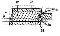
도 1에 도시된 바와 같이, 전도체(12)는 하나의 밀봉 영역(14)을 구비하고, 이에 따라 전지(도시되지 않음)의 패키지로부터 돌출되는 전도체(12)는 패키지와 빈틈없이 밀봉된다.As shown in FIG. 1, the
도 2는 상기 밀봉 영역(14)을 구비하는 도 1의 전도체의 확대 사시도이다.2 is an enlarged perspective view of the conductor of FIG. 1 with the sealing
판상의 전도체(12)는 직육면체로서 묘사되고, 이는 반드시 평행하지는 않는 서로 대향하는 제1 표면(16)과 제2 표면(17)을 포함하고 있다. 두 개의 표면(16, 17)은 가장 큰 넓이를 가지고 전도체(12)의 주요 표면을 형성하며, 도 1에 도시된 바와 같이, 기본적으로 상기 전극(10)의 주 확장면에 대하여 평행하게 배열된다. 상기 두 개의 표면은 기본적으로는 서로 대향하지만 반드시 서로 평행하지는 않는 제1 측면(18) 및 제2 측면(19)에 의해 표시된다.The plate-
판상의 직육면체는 상기 두 개의 표면(16, 17)을 상호 연결하는 두 개의 추가적인 측면(20)을 더욱 포함한다(도 2). 이것들은 전도체(12)와 전극(10)의 사이, 또는 일측에 있는 그것의 전극 컬렉터와 타측에 있는 상기 갈바니 전지의 연결 장치 사이의 전기적 접촉에 사용된다.The plate-shaped cuboid further comprises two
전도체(12)는 상기 갈바니 전지의 패키지와 빈틈없이 밀봉되는 하나의 밀봉 영역(14)을 구비한다. 이 밀봉 영역은 상기 제1 및 제2 표면(16, 17)의 둘레와 상기 제1 및 제2 측면(18, 19)의 둘레를 일정한 부분 높이(h)로, 즉 전도체(12)의 전체 높이(H)를 넘지 않는 높이로 둘러싸고 있다.The
밀봉 영역(14)이 상기 두 개의 표면(16, 17)의 모서리와 두 개의 측면(18, 19)에 대하여 평행하더라도, 이는 필수적인 것은 아니고, 상기 밀봉 영역(14)의 경로는 상기 전지 패키지의 구성에 대하여 조절될 수 있다. 또한 상기 밀봉 영역(14)의 두께(b)는 도 2에 도시되어 있는 바와 같이 상기 전도체(12)의 전체 범위에 걸쳐서 일정해야 하는 것은 아니다.Although the sealing
도 3은 밀봉 영역(14) 내에 밀봉층(22)을 갖는 도 1의 전도체(12), 즉 미리 밀봉되어 있는 전도체(12)의 확대 사시도이다.FIG. 3 is an enlarged perspective view of the
도 2의 실시예에 있어서는 전도체(12)가 전지의 패키지를 밀봉하는 단지 하나의 밀봉 영역(14)만을 포함하고 있는 것과 달리, 도 3에 도시된 실시예의 경우에는 밀봉층(22)이 전도체의 밀봉 영역(14)에 추가된다. 상기 밀봉층(22)은 예를 들어 하나의 밀봉 띠 또는 하나의 밀봉 필름 형태로 열 공정을 통하여 상기 전도체(12)에 결합된다. 탭(tab, 날개)은 전도체(12)의 두 개의 측면(18) 영역에 형성되는데, 이 경우에 두 개의 밀봉 띠 내지 밀봉 필름(22)은 직접적으로 함께 결합된다.In the embodiment of FIG. 2, the
상기 밀봉층(22)은 고융점 플라스틱 재료로 이루어져 있으며, 이는 화학적으로 적합하고, 갈바니 전지의 내용물에 대해 비활성이다. 상기 밀봉층(22)을 위한 적합한 재료는 예를 들어 폴리에틸렌, 폴리프로필렌, 폴리이미드, 폴리에틸렌 테레프탈레이트, PVC, PDFE 또는 이들의 임의의 .조합물을 포함한다. 상기 밀봉층(22)은 예를 들어 대략 0.02 mm 내지 대략 0.3 mm의 범위, 바람직하게는 대략 0.05 mm 내지 대략 0.2 mm의 범위, 더욱 바람직하게는 대략 0.1 mm의 두께(t)를 갖는다. 상기 밀봉층(22)의 너비는 기본적으로 전도체(12)의 밀봉 영역(14)의 너비(b)에 대응한다.The
도 3의 실시예에서 상기 전도체(12)의 나머지 특징은 앞에서 설명한 도 2의 실시예와 동일하다.The remaining features of the
도 2 또는 도 3의 전도체(12)는 길이(L)와 높이(H) 및 두께(D)를 갖는다. 길이(L)는 두 개의 측면(18, 19) 사이의 거리로 정의되고, 높이(H)는 두 개의 측면(20) 사이의 거리로 정의되며, 두께(D)는 두 개의 표면(16, 17) 사이의 거리에 의해 정의된다. 여기서, 상기 두 개의 표면(16, 17)에 의해 정의되는 전도체의 두께(D)는 만일 상기 두 개의 표면(16, 17)이 기본적으로 서로 평행하게 배열되는 경우에는 예컨대 그것의 두 개의 측면 영역 사이의 일정한 두께가 될 수 있다. 또한, 상기 두 개의 표면(16, 17)이 서로 평행하지 않게 배열된 경우에는 상기 전도체(12)의 두께(D) 또한 상기 두 개의 측면 영역 사이의 최대 두께로서 또는 상기 두 개의 측면 사이의 평균 두께로서 정의될 수 있다.The
본 발명의 실시예에 있어서, 전도체(12)는 구리로 구성거나(애노드에 결합되는 경우) 알루미늄으로 구성되고(캐소드에 결합되는 경우), 예컨대 대략 0.3 mm(구리) 내지 0.5 mm(알루미늄)의 두께(D)와, 대략 35 mm의 높이(H) 및, 대략 105 mm의 길이(L)를 갖는다. 그리고 상기 밀봉 영역(14) 또는 밀봉층(15)이 각각 대략 7 mm의 너비(b)를 가지고, 예컨대 상기 전도체(12)의 하부 모서리로부터 대략 5 mm 내지 10 mm의 거리 만큼 추가될 수 있다.In an embodiment of the invention, the
전도체(12)와 갈바니 전지의 패키지 사이의 밀봉은 전도체(12)의 실시예에 따라서 다르게 이루어질 수 있다.The sealing between the
제1 실시예에 있어서, 전도체(12)는 단지 밀봉 영역(14)만을 포함하고, 미리 밀봉되어 있는 밀봉층(22)은 포함하고 있지 않다. 만일 갈바니 전지의 패키지가 단지 밀봉 영역만을 포함하지 않는다면, 두 개의 구성 요소 사이의 밀봉은 그 사이에 개재된 별도의 밀봉층을 통하여, 또는 적절한 패키지 재료의 경우에는 두 개의 구성 요소 사이에서 직접적으로 이루어질 수 있다.In the first embodiment, the
제2 실시예에 있어서는, 전도체(12)는 단지 밀봉 영역(14)만을 포함하여 구성되고(도 2 참조), 패키지의 대응하는 밀봉 영역이 밀봉층과 미리 밀봉되어, 전도체(12)와 패키지 사이의 밀봉이 패키지의 밀봉층을 통하여 이루어질 수 있도록 되어 있다.In the second embodiment, the
더우기, 도 3에 따른 제3 실시예에 있어서는, 전도체(12)는 밀봉 영역(14) 내의 밀봉층(22)을 제공한다. 이에 따라서 갈바니 전지의 패키지는 밀봉 영역 내에서 별도의 자체 밀봉층을 필요로 하지 않는데, 그 이유는 상기 두 개의 구성 요소 사이의 밀봉이 미리 밀봉되어 있는 밀봉층(22)에 의해 전도체(12)상에서 실현되기 때문이다.Furthermore, in the third embodiment according to FIG. 3, the
또 다른 실시예로서, 전지 패키지의 밀봉 영역에 밀봉층을 제공함과 더불어 전도체(12)의 밀봉 영역에 밀봉층(22)을 제공할 수 있다. 이 경우에는 전도체와 패키지상의 2개의 밀봉층을 연결함으로써 밀봉이 이루어지게 된다.In another embodiment, the
도 4a 및 도 4b를 참고하여 기본적으로 사각형상의 단면을 갖는 종래 전도체의 문제점을 설명한다.4A and 4B, the problem of the conventional conductor having a basically rectangular cross section will be described.
도 4a는 밀봉 영역(14) 또는 밀봉층(22)의 영역 내에서 각각 대략 최대 0.2 mm의 평균 두께(D)를 갖는 비교적 얇은 전도체를 나타낸 것이다. 도 4a에 도시된 바와 같이, 밀봉층(22)은 이러한 작은 두께로 인하여 전도체(12)의 측면(18, 19) 영역에 잘 부착된다.4A shows a relatively thin conductor having an average thickness D of approximately up to 0.2 mm each in the region of sealing
그러나, 도 4b에 도시된 바와 같이, 두꺼운 전도체(12)의 경우에는 빈틈 영역이 연속적인 채널(26)의 형태로 양 측면(18, 19)에 형성될 수 있다. 또한 전도체(12)가 이 영역 내에서 밀봉되는 갈바니 전지의 패키지는 필수적으로 직각의 굴곡부(28)를 지지하여야 하는데, 이 위치에서 당연히 패키지의 수명이 저하되게 된다. 밀봉에 있어서의 이러한 약한 부위는 특히 전도체(12)의 높은 충전 전류 및 방전 전류시와 이와 관련된 고온 중에 밀봉의 안전성 및 보존성을 더욱 축소시키게 된다.However, as shown in FIG. 4B, in the case of
종래의 전도체에 있어서의 이와 같은 문제들을 줄이기 위해 갈바니 전지용 전도체(12)를 변경할 필요가 있다.It is necessary to modify the
도 5 내지 도 15를 참고로, 본 발명에 따른 전도체(12)의 여러 가지 실시예를 상세히 설명하기로 한다. 이 경우, 도시된 모든 전도체(12)는 밀봉층을 포함하거나 포함하지 않고 구현될 수 있다.5 to 15, various embodiments of the
도 5의 제1 실시예에 있어서, 측면(18) 영역에 전체적으로 세 개의 영역 부분(24a, 24b, 24c)이 형성되어 있다. 세 개의 영역 부분(24a, 24b, 24c)은 기본적으로 평평한 표면으로 형성되는 한편, 상기 제1 및 제3 영역 부분(24a, 24c)은 각각 한편으로는 인접해 있는 표면(16, 17)과 통합되고(합쳐지고) 다른 한편으로는 제2 영역 부분(24b)과 통합된다. 각 영역 부분(24a, 24b, 24c)의 사이와 표면(16, 17)과의 사이의 경로는 예컨대 모서리(그러나, 각각 90°이상의 둔각을 형성하는)에 의해 형성되는 불연속성이 있다. 또한, 이들 경로는 연속적으로, 즉 원호 형상으로 또는 연속적으로 변화되는 경로로서 형성될 수 있다.In the first embodiment of Fig. 5, three
이 세 개의 영역 부분(24a, 24b, 24c)에 의해 전도체(12)의 측면(19) 영역 에서 감소된 두께를 갖는 단면이 형성되는데, 그것의 두께(d)는 단면상 상기 전도체(12)의 상기 두께(D)와 비교할 때 상기 두 개의 측면(18, 19) 영역 사이에서 감소되어 있다. These three
도 5에 명확하게 도시된 바와 같이, 전도체(12)의 구성에 있어서, 상기 밀봉층(22)은 상기 전도체(12)가 더욱 큰 두께(D)를 갖는 경우에도 역시 단단하고 안전하게 전도체(12)의 측면(18, 19)에 결합될 수 있다. 또한 패키지는 측면(18, 19)의 영역에서 심하게 굴곡되지 않기 때문에 패키지의 안정성 및 보존성 역시 향상되어 있다.As clearly shown in FIG. 5, in the configuration of the
도 5의 실시예에 있어서, 감소된 두께(d)는 역시 전도체(12)의 최소 두께가 되고, 이는 도 5에 도시된 바와 같이 측면(18)의 가장 바깥쪽 가장자리 영역에 자리 잡고 있다.In the embodiment of FIG. 5, the reduced thickness d is also the minimum thickness of the
두 개의 영역 부분(24a, 24c)은 각각의 표면에 대하여 평균 경사 각도 α로 기울어져 있다. 이 경사 각도 α는 예를 들어 대략 15° 내지 대략 40° 사이의 범위, 더욱 바람직하게는 대략 20° 내지 대략 30°의 범위, 가장 바람직하게는 대략 30°이다. 도 5에서 상기 두 개의 영역 부분(24a, 24c)이 각각 동일한 경사 각도 α로 도시되어 있다 하더라도, 상기 두 개의 표면 부분(24a, 24c)을 측면(18)의 범위 내에서 여러 가지 경사 각도 α로 형성할 수 있음은 당연하다.The two
도 6에 도시된 제2 실시예는 측면(18) 영역이 단면상 대칭적이지 않고 비대칭적으로 형성되어 있다는 점에서 상기한 제1 실시예와 차이를 보인다.The second embodiment shown in FIG. 6 differs from the first embodiment described above in that the
특히 상기 측면(18) 영역 내에서 감소된 두께(d)를 갖는 부분은 두 개의 영역 부분(24a, 24b)에 의하여 이루어지는데, 이들은 각각 평평한 표면으로 형성되고, 상호 또한 표면(16, 17)과 불연속적으로 통합된다.In particular, the portion with reduced thickness d in the region of the
도 7에 도시된 제3 실시예는, 상기 측면(18) 영역에서 감소된 두께를 갖는 부분이 세 개가 아니라 전체적으로 다섯 개의 영역 부분(24a~24e)으로 이루어지고, 이들은 각각 기본적으로 직각을 포함한다는 점에서 상기한 제1 실시예와 차이를 보인다. 따라서, 상기 감소된 두께(d)는 상기 두 개의 영역 부분(24b, 24d)의 사이로 정의된다.In the third embodiment shown in FIG. 7, the portion having the reduced thickness in the region of the
본 실시예의 비대칭적 대안으로서, 예를 들어 도 7에 도시된 상기 두 개의 영역 부분(24d, 24e)을 도 5에 도시된 상기 제3 영역 부분(24c)으로 대체하는 것도 역시 가능하다.As an asymmetric alternative to this embodiment, it is also possible to replace the two
도 8에 도시된 제4 실시예는, 상기 측면(18) 영역에서 감소된 두께를 갖는 부분을 이루고 있는 제1 및 제3 영역 부분(24a, 24c)이 평탄면이 아니라 각각 굴곡면으로 형성되어 있다는 점에서 상기한 제1 실시예와 차이를 보인다. 상기 두 개의 굴곡면은 각각 오목한 굴곡을 가진 부분뿐만 아니라 볼록한 굴곡을 가진 부분도 역시 포함하고 있으며, 이것들은 연속적으로 통합된다. 더우기 상기 두 개의 영역 부분(24a, 24c)은 연속적으로 전도체의 표면(16, 17)과 통합되고 불연속적으로 제2 영역 부분(24b)과 통합된다. 또한 상기 통합 부위들은 제1 및 제3 영역 부분(24a, 24c)과 제2 영역 부분(24b)의 사이에서 연속, 즉 만곡될 수 있다.In the fourth embodiment shown in FIG. 8, the first and
본 실시예의 비대칭적인 대안으로서, 예를 들어 도 8에 도시된 상기 굴곡진 제3 영역 부분(24c)을 도 5에 도시된 평평한 표면 부분(24c)으로 대체하는 것도 역시 가능하다.As an asymmetric alternative to this embodiment, it is also possible to replace the curved
도 9에 도시된 제5 실시예에 있어서는 측면(18) 영역에 단지 하나의 영역 부분(24a)이 형성되어 있으며, 이에 따라서 볼록하게 만곡되어 있다. 이 경우, 상기 영역 부분은 일정한 곡률반경뿐만 아니라 다양한 곡률반경을 갖도록 하는 것이 가능하다.In the fifth embodiment shown in FIG. 9, only one
도 10에 도시된 제6 실시예는 상기한 제4 실시예 및 제5 실시예의 결합이 될 수 있다. 예를 들어, 상기 제1 및 제3 영역 부분(24a, 24c)이 굴곡진 표면으로 형성된 도 8의 제4 실시예를 근거로, 본 실시예에 있어서 상기 제2 영역 부분(24b)은 평평한 표면이 아니라(도 8) 볼록하게 굴곡진 표면으로(도 9) 형성된다.The sixth embodiment shown in FIG. 10 may be a combination of the fourth and fifth embodiments described above. For example, based on the fourth embodiment of FIG. 8 in which the first and
도 11에 도시된 제7 실시예는 도 5의 제1 실시예의 변형으로서 또는 도 8의 제4 실시예의 변형으로서 간주할 수 있다. 특히, 상기 측면(18) 영역에서 감소된 두께를 갖는 부분은 전체적으로 세 개의 영역 부분(24a, 24b, 24c)에 의해 단면상 기본적으로 대칭적인 형태로 형성되어 있다. 상기 제2 영역 부분(24b)이 평평한 표면으로 형성된 것과 달리, 서로 인접하고 있는 상기 두 개의 영역 부분(24a, 24c)은 오목하게 만곡된 표면으로서 형성되어 있다. 상기 영역 부분(24a, 24b, 24c) 사이 그리고 상기 표면(16, 17)에 대한 상기 통합 영역은 각각 불연속적으로, 다시 말해 각이 진 형상(모서리)으로 구성되어 있다.The seventh embodiment shown in FIG. 11 can be regarded as a modification of the first embodiment of FIG. 5 or as a modification of the fourth embodiment of FIG. 8. In particular, the portion with reduced thickness in the region of the
도 12에 도시된 제8 실시예에 있어서는 판상의 전도체(12)의 측면(18) 영역에서 감소된 두께를 갖는 부분이 두 개의 영역 부분(24a, 24b)을 통하여 형성되어 있고, 이들 각각은 평평한 표면으로 형성되어 있으며 단면형상이 기본적으로 삼각형상을 이루도록 서로 통합된다. 상기 측면(18)은 이와 같은 대칭적인 실시예로부터 벗어나서 상기 두 개의 영역 부분(24a, 24b)을 여러 가지 경사 각도 α를 이용하여 어느 한쪽의 표면(16, 17)측으로 기울이는 것도 역시 가능하다.In the eighth embodiment shown in FIG. 12, a portion having a reduced thickness in the region of the
도 13에 도시된 상기 제9 실시예는 상기한 도 6의 제2 실시예의 변형이다. 상기 제2 실시예의 경우와 마찬가지로, 이 경우에 있어서도 역시 측면(18) 영역의 비대칭적인 구성이 제공되어 있다. 감소된 두께를 갖는 부분은 볼록하게 굴곡진 표면으로서 이루어져 있는 제1 영역 부분(24a)을 통하여 그리고 기본적으로 평평한 표면으로 이루어져 있는 제2 영역 부분(24b)을 통하여 형성된다. 상기 제1 영역 부분(24a)과 제1 표면(16) 및, 제1 영역부분(24a)과 제2 영역 부분(24b) 사이의 경로 부분들은 연속적으로 형성되는 반면에 전도체(12)의 제2 표면(17)과 제2 영역 부분(24b) 사이의 경로 부분은 불연속적으로 형성되어 있다.The ninth embodiment shown in FIG. 13 is a modification of the second embodiment of FIG. 6 described above. As in the case of the second embodiment, an asymmetrical configuration of the
제10 실시예로서, 도 14는 측면(18) 영역에서 비대칭적인 구성의 단면을 갖는 전도체(12)를 도시하고 있다. 감소된 두께를 갖는 부분을 형성하기 위하여 세 개의 영역 부분(24a, 24b, 24c)이 제공되어 있는데, 이는 각각 굴곡진 표면으로서 형성되어 있으며 상기 전도체(12)의 표면(16, 17)에 대해서 뿐만 아니라 그것들 사이에서도 역시 연속적인 경로가 제공될 수 있다. 상기 제1 및 제2 영역 부분(24a, 24c)은 각각 볼록한 표면으로서 형성되어 있고, 그 사이에 개재된 제2 영역 부분(24b)은 오목한 표면으로서 형성되어 있다. 이때, 선택적으로 제2 영역 부분(24b)에 의해 상기 실시예와 달리 감소된 두께를 갖는 부분의 최소 두께가 전도체(12)의 가장 바깥쪽 가장자리에 놓여 있지 않도록 단면이 수축된 부분(constriction)이 형성될 수 있다.As a tenth embodiment, FIG. 14 shows a
도 15에 도시된 제11 실시예는 전도체(12)의 측면(18) 영역에서 기본적으로 대칭적인 구성의 단면을 갖는다. 도 8의 상기 실시예에 대한 변형으로서, 상기 제1 및 제3 영역 부분(24a, 24b)은 여러 차례 굴곡진 표면으로서 형성되어 있으며, 도 15에 도시된 바와 같이, 단면상 양측에 수축된 부분이 형성된다. 이와 같은 두 개의 영역 부분(24a, 24c) 사이에 개재된 제2 영역 부분(24b)은 기본적으로 평평한 표면으로 형성되어 있다. 또한 다른 실시예에 있어서, 감소된 두께를 갖는 부분에서의 이와 같은 수축은 일측에만 제공될 수도 있다.The eleventh embodiment shown in FIG. 15 has a cross section of a basically symmetrical configuration in the region of the
이상으로 본 발명에 따른 전도체(12)에 대하여 여러 가지 실시예를 통하여 상세하게 설명하였다. 그러나, 첨부된 청구항을 통하여 정의되는 본 발명의 보호 범위를 벗어나지 않는 범위내에서, 도시된 상기 실시예를 근거로 당 분야의 전문가가 다른 여러 가지 변형 및 변경을 찾아 낼 수 있다는 것은 자명하다.The
특히 도 5 내지 도 15에 도시된 상기 전도체(12)의 실시예들은 임의적인 방식으로 결합을 할 수 있다. 이 경우에 단지 두 개 또는 그 이상의 구성도 역시 서로 결합할 수 있다.In particular, the embodiments of the
도 5 내지 도 15에 도시된 상기 전도체(12)의 단면 구성은 적어도 기본적으로 상기 전도체의 밀봉 영역(14)의 부분 높이(b)를 통하여 연장된다. 그렇지만 본 발명에 따른 전도체(12)의 제조를 더욱 단순화하기 위하여, 도시된 단면 구성을 각각 전도체(12)의 전체 높이(H)에 걸쳐 제공하는 것 역시 유리할 수 있다.The cross-sectional configuration of the
도 5 내지 도 15는 각각 전도체(12)의 하나의 측면(19)에 인접한 영역만을 도시하고 있다. 그러나, 다른 측면(18)도 바람직하게는 전도체(12)의 두께(D)와 비교할 때 감소된 두께(d)를 갖는 부분을 포함하는 단면 구성으로 제공될 수 있다. 이 경우, 상기 두 개의 측면 영역은 선택적으로 대칭적으로 형성되어 있을 수 있으며, 다시 말해 각각 동일한 단면 구성으로 또는 비대칭적으로, 다시 말해 서로 다른 구성으로 형성될 수 있는데, 이 경우에 도 5 내지 도 15에 있는 임의의 결합 그리고 또 다른 결합이 가능하다.5 to 15 only show regions adjacent to one
도 5의 상기 실시예에서 설명된 상기 측면(18, 19)의 영역 내에서의 상기 평균 경사 각도 α는 다른 모든 실시예에 대하여, 다시 말해 굴곡진 표면을 갖는 표면 부분을 가진 경우에 대해서도 역시 적용된다.
The average tilt angle α in the region of the side surfaces 18, 19 described in the embodiment of FIG. 5 applies also to all other embodiments, in other words also with the case of having a surface portion with a curved surface. do.
Claims (34)
상기 판형상의 전도체가 상기 제1 및/또는 제2 측면(18, 19)의 영역 내에서, 그 단면의 두께가 상기 전도체의 제1 및 제2 표면(16, 17)에 의하여 정의되는 두께(D)와 비교할 때 감소되고, 적어도 상기 전도체의 밀봉 영역(14)을 통하여 연장되는 부분을 갖는 것을 특징으로 하는 판상의 갈바니 전지용 전도체.In the galvanic plate-like conductor 12 which faces each other and comprises a first surface 16 and a second surface 17 connected to each other via a first side 18 and a second side 19,
The thickness D of the plate-shaped conductor in the region of the first and / or second side surfaces 18, 19 is defined by the first and second surfaces 16, 17 of the conductor. A galvanic cell conductor, characterized in that it has a portion which is reduced in comparison with) and extends at least through the sealing region (14) of the conductor.
상기 제1 및/또는 제2 측면(18, 19)의 영역 내에서 감소된 두께(d)를 갖는 부분은 상기 제1 또는 상기 제2 측면(18, 19)의 전체 높이에 걸쳐 연장되는 것을 특징으로 하는 갈바니 전지용 전도체.The method of claim 1,
The portion with reduced thickness d in the region of the first and / or second side 18, 19 extends over the entire height of the first or second side 18, 19. Galvanic cell conductor.
상기 제1 및/또는 제2 측면(18, 19)의 영역 내에서 감소된 두께(d)를 갖는 부분은 상기 전도체(12)의 상기 밀봉 영역(14)에 걸쳐 연장된 것을 특징으로 하는 갈바니 전지용 전도체.The method of claim 1,
For galvanic cells characterized in that the portion with reduced thickness d in the region of the first and / or second side surfaces 18, 19 extends over the sealing region 14 of the conductor 12. conductor.
상기 제1 및/또는 제2 측면(18, 19)의 영역 내에서 감소된 두께(d)를 갖는 부분은 상기 제1 및 제2 표면(16, 17)으로 통합되는 영역 부분(24)에 의하여 형성되는 것을 특징으로 하는 갈바니 전지용 전도체.4. The method according to any one of claims 1 to 3,
The portion with reduced thickness d in the region of the first and / or second side 18, 19 is by means of the region portion 24 which is incorporated into the first and second surfaces 16, 17. Conductor for galvanic battery, characterized in that formed.
상기 제1 및/또는 제2 측면(18, 19)의 영역 내에서 감소된 두께(d)를 갖는 부분은 한편으로는 서로 통합되고 다른 한편으로는 상기 제1 및 제2 표면(16, 17)으로 통합되는 적어도 두 개의 표면 부분(24)에 의하여 형성되는 것을 특징으로 하는 갈바니 전지용 전도체.4. The method according to any one of claims 1 to 3,
The parts with reduced thickness d in the region of the first and / or second sides 18, 19 are integrated with one another on the one hand and the first and second surfaces 16, 17 on the other hand. A galvanic cell conductor, characterized in that it is formed by at least two surface portions (24) integrated into the.
상기 제1 및/또는 제2 측면(18, 19)의 영역 내에서 감소된 두께(d) 부분의 영역 부분(들)(24)은 기본적으로 평평한 표면으로 형성되는 것을 특징으로 하는 갈바니 전지용 전도체.The method according to any one of claims 1 to 5,
Conductor for galvanic cells, characterized in that the region part (s) of the reduced thickness (d) portion in the region of the first and / or second side (18, 19) is formed essentially on a flat surface.
상기 제1 및/또는 제2 측면(18, 19)의 영역 내에서 감소된 두께(d)를 갖는 부분의 영역 부분(들)(24)은 기본적으로 굴곡진 표면(들)으로 형성되는 것을 특징으로 하는 갈바니 전지용 전도체.The method according to any one of claims 1 to 5,
The region part (s) 24 of the part with the reduced thickness d in the region of the first and / or second side 18, 19 is basically formed of curved surface (s). Galvanic cell conductor.
상기 제1 및/또는 제2 측면(18, 19)의 영역 내에서 감소된 두께(d)를 갖는 부분의 영역 부분(들)(24)은 기본적으로 평평한 표면으로 형성된 측면 부분과 굴곡진 표면으로 형성된 측면 부분을 포함하는 것을 특징으로 하는 갈바니 전지용 전도체.The method according to any one of claims 1 to 3 and 5,
The area part (s) 24 of the part having the reduced thickness d in the area of the first and / or second side 18, 19 is basically a side surface and a curved surface formed of a flat surface. A galvanic cell conductor comprising a formed side portion.
상기 굴곡진 표면(들)은 오목하게 굴곡진 표면(들)으로 형성된 것을 특징으로 하는 갈바니 전지용 전도체.The method according to claim 7 or 8,
And said curved surface (s) are formed as concave curved surface (s).
상기 굴곡진 표면(들)은 볼록하게 굴곡진 표면(들)으로 형성된 것을 특징으로 하는 갈바니 전지용 전도체.The method according to claim 7 or 8,
And said curved surface (s) are formed as convexly curved surface (s).
상기 굴곡진 표면(들)은 부분적으로 볼록하게 그리고 부분적으로 오목하게 굴곡진 표면(들)으로 형성된 것을 특징으로 하는 갈바니 전지용 전도체.The method according to claim 7 or 8,
And wherein said curved surface (s) are formed as partially convex and partially concave curved surface (s).
상기 제1 및/또는 제2 측면(18, 19)의 영역 내에서 감소된 두께(d)를 갖는 부분의 영역 부분(들)(24)은 제1 또는 제2 표면(16, 17)과 비교할 때 대략 15° 내지 대략 40° 범위의 평균 경사 각도(α)로 기울어져 형성된 것을 특징으로 하는 갈바니 전지용 전도체.The method according to any one of claims 1 to 11,
The area part (s) 24 of the part with the reduced thickness d in the area of the first and / or second side 18, 19 may be compared with the first or second surface 16, 17. And when formed at an angle of inclination (α) in the range of approximately 15 ° to approximately 40 °.
상기 제1 및/또는 제2 측면(18, 19)의 영역 내에서 감소된 두께(d)를 갖는 부분의 영역 부분(들)(24)은 제1 또는 제2 표면(16, 17)과 비교할 때 대략 20° 내지 대략 30° 범위의 평균 경사 각도(α)로 기울어져 형성된 것을 특징으로 하는 갈바니 전지용 전도체.The method of claim 12,
The area part (s) 24 of the part with the reduced thickness d in the area of the first and / or second side 18, 19 may be compared with the first or second surface 16, 17. And when inclined at an average inclination angle [alpha] in the range of about 20 [deg.] To about 30 [deg.].
상기 제1 및/또는 제2 측면(18, 19)의 영역 내에서 감소된 두께(d)를 갖는 부분은 기본적으로 대칭적인 단면을 갖고 형성된 것을 특징으로 하는 갈바니 전지용 전도체.The method according to any one of claims 1 to 13,
A part having a reduced thickness (d) in the region of the first and / or second side (18, 19) is basically formed with a symmetrical cross section.
상기 제1 및/또는 제2 측면(18, 19)의 영역 내에서 감소된 두께(d)를 갖는 부분은 기본적으로 비대칭적인 단면을 갖고 형성된 것을 특징으로 하는 갈바니 전지용 전도체.The method according to any one of claims 1 to 13,
A part having a reduced thickness (d) in the region of the first and / or second side (18, 19) is formed with an essentially asymmetric cross section.
상기 제1 측면(18)의 상기 영역 및 상기 제2 측면(19)의 상기 영역은 단면상 서로 대칭적으로 형성된 것을 특징으로 하는 갈바니 전지용 전도체.The method according to any one of claims 1 to 15,
The region of the first side (18) and the region of the second side (19) are symmetrical to each other in cross section, characterized in that the galvanic cell conductor.
상기 제1 측면(18)의 상기 영역 및 상기 제2 측면(19)의 상기 영역은 단면상 서로 비대칭적으로 형성된 것을 특징으로 하는 갈바니 전지용 전도체.The method according to any one of claims 1 to 15,
The region of the first side (18) and the region of the second side (19) are formed asymmetrically with respect to each other in cross section.
상기 영역 부분(24)들 및 상기 표면(16, 17)들 사이의 경로 영역 및/또는 몇 개의 영역 부분(24)들 사이의 경로 영역은 단면상 서로 연속적으로 형성된 것을 특징으로 하는 갈바니 전지용 전도체.The method according to any one of claims 1 to 17,
The path region between the region portions (24) and the surfaces (16, 17) and / or the path region between several region portions (24) are formed contiguously with one another in cross section.
상기 영역 부분(24)들 및 상기 표면(16, 17)들 사이의 중첩 영역 및/또는 몇 개의 영역 부분(24)들 사이의 중첩 영역은 단면상 서로 불연속적으로 형성된 것을 특징으로 하는 갈바니 전지용 전도체.The method according to any one of claims 1 to 17,
The overlapping region between the region portions (24) and the surfaces (16, 17) and / or the overlapping region between several region portions (24) are formed discontinuously from one another in cross section.
상기 전도체(12)는 상기 밀봉 영역(14) 내에서 하나의 밀봉층(22)을 포함하는 것을 특징으로 하는 갈바니 전지용 전도체.The method according to any one of claims 1 to 19,
The conductor (12) is a galvanic cell conductor, characterized in that it comprises one sealing layer (22) in the sealing area (14).
상기 밀봉층(22)은 상기 전도체(12)의 상기 제1 및 제2 표면(16, 17) 그리고 상기 제1 및 제2 측면(18, 19)의 주위를 둘러싸는 것을 특징으로 하는 갈바니 전지용 전도체.The method of claim 20,
The sealing layer 22 surrounds the first and second surfaces 16 and 17 and the first and second side surfaces 18 and 19 of the conductor 12. .
상기 밀봉층(22)은 플라스틱으로 형성된 것을 특징으로 하는 갈바니 전지용 전도체.The method of claim 20 or 21,
The sealing layer 22 is a galvanic cell conductor, characterized in that formed of plastic.
상기 밀봉층(22)은 폴리에틸렌, 폴리프로필렌, 폴리이미드, 폴리에틸렌 테레프탈레이트, PVC, PDFE 또는 이들의 임의의 결합으로 형성된 것을 특징으로 하는 갈바니 전지용 전도체.The method of claim 22,
The sealing layer 22 is a galvanic cell conductor, characterized in that formed of polyethylene, polypropylene, polyimide, polyethylene terephthalate, PVC, PDFE or any combination thereof.
상기 밀봉층(22)은 대략 0.02 mm 내지 대략 0.3 mm 범위의 두께를 갖는 것을 특징으로 하는 갈바니 전지용 전도체.The method according to any one of claims 20 to 23, wherein
The sealing layer (22) is galvanic cell conductor, characterized in that having a thickness in the range of about 0.02 mm to about 0.3 mm.
상기 밀봉층(22)은 대략 0.05 mm 내지 대략 0.2 mm 범위의 두께(t)를 갖는 것을 특징으로 하는 갈바니 전지용 전도체.25. The method of claim 24,
The sealing layer (22) is galvanic cell conductor, characterized in that having a thickness (t) in the range of about 0.05 mm to about 0.2 mm.
상기 밀봉 영역(14) 또는 상기 밀봉층(22)은 대략 4 mm 내지 대략 15 mm 범위의 너비(b)를 갖는 것을 특징으로 하는 갈바니 전지용 전도체.The method according to any one of claims 1 to 25,
The sealing region (14) or the sealing layer (22) has a width (b) in the range of about 4 mm to about 15 mm.
상기 밀봉 영역(14) 또는 상기 밀봉층(22)은 대략 6 mm 내지 대략 10 mm 범위의 너비(b)를 갖는 것을 특징으로 하는 갈바니 전지용 전도체.The method of claim 26,
The sealing region (14) or the sealing layer (22) has a width (b) in the range of about 6 mm to about 10 mm.
상기 제1 및/또는 상기 제2 전도체는 제1항 내지 제27항 중 어느 항에 따른 전도체(12)인 것을 특징으로 하는 갈바니 전지.In a galvanic cell comprising a first electrode coupled to the first conductor, a second electrode coupled to the second conductor, and a separator interposed between the first and second electrodes,
A galvanic cell, characterized in that the first and / or the second conductor is the conductor (12) according to any one of claims 1 to 27.
상기 갈바니 전지는 교대로 적층되어 있고 각각 하나의 세퍼레이터에 의하여 분리되어 있는 다수의 제1 전극 및 다수의 제2 전극의 더미를 포함하는 것을 특징으로 하는 갈바니 전지.The method of claim 28,
The galvanic cell is a galvanic cell, characterized in that it comprises a plurality of first electrode and a plurality of piles of a plurality of second electrodes which are alternately stacked and separated by one separator.
상기 제1 및 제2 전극(들) 그리고 상기 세퍼레이터(들)은 하나의 패키지 내에 수납되며, 이를 통해 상기 제1 및 제2 전도체가 돌출되고, 하나의 밀봉 영역을 형성하며.
상기 제1 및/또는 제2 전도체는 제20항 내지 제27항 중 한 항에 따른 전도체(12)로 형성됨과 더불어, 상기 전도체 및 패키지의 밀봉 영역 내에서 밀봉층(22)을 통하여 상기 패키지와 밀봉되어 있는 것을 특징으로 하는 갈바니 전지.30. The method of claim 28 or 29,
The first and second electrode (s) and the separator (s) are housed in one package, through which the first and second conductors protrude and form one sealing area.
The first and / or second conductors are formed from the conductors 12 according to one of claims 20 to 27, in addition to the package and through the sealing layer 22 in the sealing area of the conductors and the package. A galvanic cell, which is sealed.
상기 제1 및 제2 전극(들) 그리고 상기 세퍼레이터(들)은 하나의 패키지 내에 수납되며, 이를 통해 상기 제1 및 제2 전도체가 돌출되고, 밀봉층에 의해 미리 밀봉된 밀봉 영역을 형성하며,
상기 제1 및/또는 제2 전도체는 제1항 내지 제19항 중 한 항에 따른 전도체(12)로 형성됨과 더불어, 상기 전도체 및 패키지의 밀봉 영역 내에서 밀봉층(22)을 통하여 상기 패키지와 밀봉되어 있는 것을 특징으로 하는 갈바니 전지.30. The method of claim 28 or 29,
The first and second electrode (s) and the separator (s) are housed in one package, through which the first and second conductors protrude and form a sealing region previously sealed by a sealing layer,
The first and / or second conductors are formed from the conductors 12 according to one of claims 1 to 19, and together with the package via a sealing layer 22 in the sealing area of the conductors and the package. A galvanic cell, which is sealed.
상기 제1 및 제2 전극(들) 그리고 상기 세퍼레이터(들)은 하나의 패키지 내에 수납되며, 이를 통해 상기 제1 및 제2 전도체가 돌출되고, 밀봉 영역을 형성하며,
상기 제1 및/또는 제2 전도체는 제1항 내지 제19항 중 한 항에 따른 전도체(12)로 형성됨과 더불어, 상기 전도체 및 상기 패키지의 밀봉 영역 내에서 직접적으로 또는 사이에 개재된 밀봉층(22)을 통하여 상기 패키지와 밀봉되어 있는 것을 특징으로 하는 갈바니 전지.30. The method of claim 28 or 29,
The first and second electrode (s) and the separator (s) are housed in one package, through which the first and second conductors protrude and form a sealing region,
The first and / or second conductor is formed from the conductor 12 according to any one of claims 1 to 19, and the sealing layer interposed directly or between the conductor and the sealing region of the package. The galvanic cell is sealed with the said package through (22).
상기 제1 및 제2 전극(들) 그리고 상기 세퍼레이터(들)은 하나의 패키지 내에 수납되며, 이를 통해 상기 제1 및 제2 전도체가 돌출되고, 밀봉 영역을 형성하며, 밀봉층에 의해 미리 밀봉되고,
상기 제1 및/또는 제2 전도체는 제20항 내지 제27항 중 한 항에 따른 전도체(12)로 형성됨과 더불어, 상기 전도체 및 패키지의 밀봉 영역 내에서 상기 전도체전도체 밀봉층(22) 및 패키지의 밀봉층을 통해 패키지와 밀봉되어 있는 것을 특징으로 하는 갈바니 전지.30. The method of claim 28 or 29,
The first and second electrode (s) and the separator (s) are housed in one package, through which the first and second conductors protrude, form a sealing area, and are previously sealed by a sealing layer. ,
The first and / or second conductors are formed of the conductors 12 according to one of claims 20 to 27, in addition to the conductor conductor sealing layer 22 and the package within the sealing region of the conductors and the package. A galvanic cell, which is sealed with a package through a sealing layer of the.
상기 갈바니 전지는 리튬 이온 전지인 것을 특징으로 하는 갈바니 전지.The method according to any one of claims 28 to 33, wherein
The galvanic battery is a galvanic battery, characterized in that the lithium ion battery.
Applications Claiming Priority (2)
| Application Number | Priority Date | Filing Date | Title |
|---|---|---|---|
| DE102007059768A DE102007059768A1 (en) | 2007-12-12 | 2007-12-12 | Current conductor for a galvanic cell |
| DE102007059768.3 | 2007-12-12 |
Publications (1)
| Publication Number | Publication Date |
|---|---|
| KR20120002402A true KR20120002402A (en) | 2012-01-05 |
Family
ID=40627395
Family Applications (1)
| Application Number | Title | Priority Date | Filing Date |
|---|---|---|---|
| KR1020107013141A KR20120002402A (en) | 2007-12-12 | 2008-12-08 | Current conductor for a galvanic cell |
Country Status (7)
| Country | Link |
|---|---|
| US (2) | US20100304211A1 (en) |
| EP (1) | EP2229701A2 (en) |
| KR (1) | KR20120002402A (en) |
| CN (1) | CN101897057A (en) |
| BR (1) | BRPI0821260A2 (en) |
| DE (1) | DE102007059768A1 (en) |
| WO (1) | WO2009074279A2 (en) |
Families Citing this family (5)
| Publication number | Priority date | Publication date | Assignee | Title |
|---|---|---|---|---|
| DE102009032523A1 (en) * | 2009-07-10 | 2011-01-20 | Li-Tec Battery Gmbh | Method for producing an electrochemical cell |
| JP2017117705A (en) * | 2015-12-25 | 2017-06-29 | 住友電気工業株式会社 | Lead member and battery employing the lead member |
| US10446803B2 (en) * | 2017-08-29 | 2019-10-15 | Robert Bosch Battery Systems Llc | Lead tab for battery terminal |
| JP7331360B2 (en) * | 2018-12-26 | 2023-08-23 | 大日本印刷株式会社 | Electrode tabs, batteries, and how to attach the electrode tabs |
| WO2020137353A1 (en) * | 2018-12-28 | 2020-07-02 | パナソニックIpマネジメント株式会社 | Battery and method for manufacturing battery |
Family Cites Families (13)
| Publication number | Priority date | Publication date | Assignee | Title |
|---|---|---|---|---|
| JP3481797B2 (en) * | 1996-10-03 | 2003-12-22 | 片山特殊工業株式会社 | Method for manufacturing battery electrode substrate and battery electrode substrate |
| JPH11204090A (en) * | 1998-01-07 | 1999-07-30 | Toshiba Battery Co Ltd | Sheet battery |
| JP2000268826A (en) * | 1999-03-19 | 2000-09-29 | Hitachi Cable Ltd | Copper material for negative electrode collector of li ion battery, and li ion battery |
| JP2000285903A (en) * | 1999-03-31 | 2000-10-13 | Sanyo Electric Co Ltd | Thin battery |
| JP2001057203A (en) * | 1999-08-19 | 2001-02-27 | Dainippon Printing Co Ltd | Tab structure of polymer battery |
| JP2002246269A (en) * | 2001-02-20 | 2002-08-30 | Kyocera Corp | Electrochemical element |
| EP1249881A3 (en) * | 2001-04-10 | 2005-08-03 | Matsushita Electric Industrial Co., Ltd. | Negative electrode material for nonaqueous electrolyte secondary battery and method for producing the same |
| WO2003069700A2 (en) * | 2002-02-12 | 2003-08-21 | Eveready Battery Company, Inc. | Flexible thin printed battery with gelled electrolyte and method of manufacturing same |
| JP3702868B2 (en) * | 2002-06-26 | 2005-10-05 | 日産自動車株式会社 | Thin battery |
| JP3758629B2 (en) * | 2002-09-26 | 2006-03-22 | 日産自動車株式会社 | Laminate sheet and laminate battery using the same |
| JP4554911B2 (en) * | 2003-11-07 | 2010-09-29 | パナソニック株式会社 | Nonaqueous electrolyte secondary battery |
| CN100405658C (en) * | 2004-07-23 | 2008-07-23 | 日本无公害电池研究所 | Nickel electrode and alkali storage battery using the same |
| JP2006164784A (en) * | 2004-12-08 | 2006-06-22 | Nec Lamilion Energy Ltd | Film-armored electric device |
-
2007
- 2007-12-12 DE DE102007059768A patent/DE102007059768A1/en not_active Withdrawn
-
2008
- 2008-12-08 EP EP08859435A patent/EP2229701A2/en not_active Withdrawn
- 2008-12-08 KR KR1020107013141A patent/KR20120002402A/en not_active Application Discontinuation
- 2008-12-08 CN CN2008801205779A patent/CN101897057A/en active Pending
- 2008-12-08 US US12/747,764 patent/US20100304211A1/en not_active Abandoned
- 2008-12-08 WO PCT/EP2008/010397 patent/WO2009074279A2/en active Application Filing
- 2008-12-08 BR BRPI0821260-0A patent/BRPI0821260A2/en not_active IP Right Cessation
-
2013
- 2013-05-23 US US13/901,072 patent/US20130302671A1/en not_active Abandoned
Also Published As
| Publication number | Publication date |
|---|---|
| CN101897057A (en) | 2010-11-24 |
| BRPI0821260A2 (en) | 2015-06-16 |
| DE102007059768A1 (en) | 2009-06-18 |
| US20130302671A1 (en) | 2013-11-14 |
| US20100304211A1 (en) | 2010-12-02 |
| WO2009074279A2 (en) | 2009-06-18 |
| EP2229701A2 (en) | 2010-09-22 |
| WO2009074279A3 (en) | 2010-07-22 |
Similar Documents
| Publication | Publication Date | Title |
|---|---|---|
| KR100894409B1 (en) | Secondary Battery Having Improved Safety by Fixing Separator to Battery Case | |
| KR101264527B1 (en) | Pouch case and battery pack using the same | |
| KR100891078B1 (en) | Lithium Secondary Battery Improved Safety and Capacity | |
| EP2750241B1 (en) | Electrode assembly having stepped levels and battery cell, battery pack, and device comprising same | |
| JP4628682B2 (en) | Battery unit and lithium secondary battery using the same | |
| KR101065379B1 (en) | Battery module | |
| KR102051109B1 (en) | Battery Module | |
| KR20130119457A (en) | Lithium secondary battery having multi-directional lead-tab structure | |
| KR20130132231A (en) | A stepwise electrode assembly, and a battery cell, battery pack and device comprising the same | |
| KR20080021271A (en) | Battery cell with small groove at surface and battery pack including the same | |
| CN101295779A (en) | Pouch type secondary battery and fabrication method thereof | |
| KR20120021194A (en) | Secondary battery of novel structure | |
| KR20110107448A (en) | Pouch-type secondary battery for preventing swelling phenomena | |
| CN107154469B (en) | Battery unit | |
| KR20170002140A (en) | Secondary Battery And Fabricating Method Thereof | |
| KR20120002402A (en) | Current conductor for a galvanic cell | |
| CN111226338B (en) | Electrode assembly, and secondary battery module including the same | |
| KR100911004B1 (en) | Battery unit and the lithium secondary battery applying the same | |
| US9142840B2 (en) | Method of reducing tabbing volume required for external connections | |
| US20040002000A1 (en) | Secondary battery | |
| US11189889B2 (en) | Rechargeable battery | |
| KR101545885B1 (en) | Electrode Assembly Having Improved Dropping Impact Stability | |
| US9012059B2 (en) | Secondary battery | |
| CN106981589B (en) | Battery unit | |
| KR101994842B1 (en) | Electrode Plate Having Structure Capable of Maximizing Interior Space Occupancy for Secondary Battery, and Secondary Battery or Capacitor Comprising the Same |
Legal Events
| Date | Code | Title | Description |
|---|---|---|---|
| A201 | Request for examination | ||
| E902 | Notification of reason for refusal | ||
| E601 | Decision to refuse application |